


High Power DPDT Switch for GSM
Description
The CXG1045N is a DPDT (Dual Pole Dual Throw)
antenna switch MMIC used in personal communication
handsets such as GSM, GSM1800 or dualband. This
IC is designed using the Sony's GaAs J-FET process.
Features
• Low insertion loss: 0.4dB (Typ.) @900MHz
0.7dB (Typ.) @1.8GHz
• High power switching P1dB:38dBm (Typ.) @900MHz
37dBm (Typ.) @1.8GHz
• Small package SSOP-8pin: (3 × 6.4 × 1.25mm)
• Low current: 200µA (Typ.)
Application
• GSM900 or GSM1800 handsets
• GSM900/GSM1800 dualband handsets
Structure
GaAs J-FET MMIC
Operating Condition
Control voltage: Vctl (H) – Vctl (L): 2.5 to 5V @Ta = 25°C
– 1 –
E98902A92-PS
Sony reserves the right to change products and specifications without prior notice. This information does not convey any license by
any implication or otherwise under any patents or other right. Application circuits shown, if any, are typical examples illustrating the
operation of the devices. Sony cannot assume responsibility for any problems arising out of the use of these circuits.
CXG1045N
8 pin SSOP (Plastic)
∗
GaAs MMICs are ESD sensitive devices. Special handling precautions are required.
For the availability of this product, please contact the sales office.
– 2 –
CXG1045N
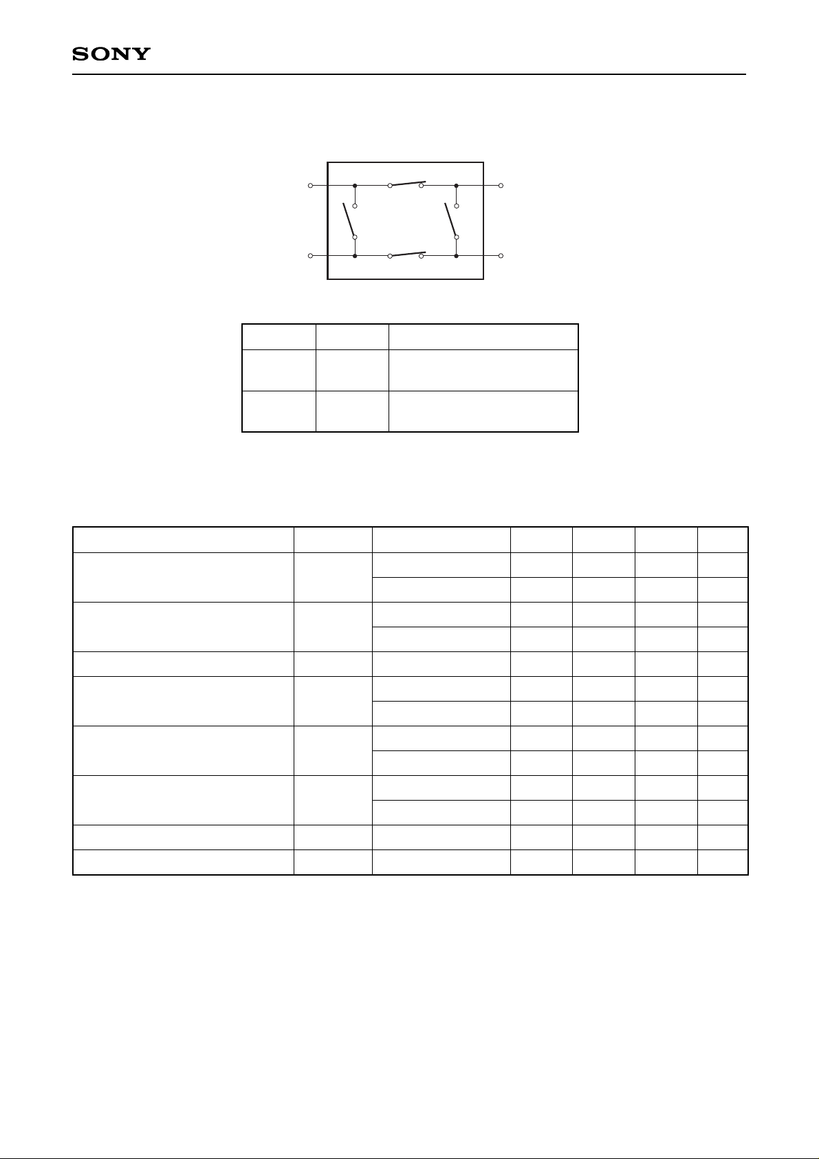
Block Diagram
RF1
RF2
RF4
RF3
VCTLA
High
Low
VCTLB
Low
High
RF1 – RF2, RF3 – RF4 ON
RF2 – RF3, RF4 – RF1 OFF
RF1 – RF2, RF3 – RF4 OFF
RF2 – RF3, RF4 – RF1 ON
Electrical Characteristics (1) (Ta = 25°C)
Min.
18
15
36
35
Typ.
0.4
0.7
21
17
1.2
38
37
100
200
Max.
0.7
1.0
1.4
–31
–31
–31
–31
500
350
Unit
dB
dB
dB
dB
dBm
dBm
dBm
dBm
dBm
dBm
ns
µA
Item
Insertion loss
Isolation
VSWR
2nd harmonics
3rd harmonics
Input power for 1dB compression
Switching time
Control current
Symbol
IL
ISO
VSWR
2fo
3fo
P1dB
TSW
I CTL
Condition
∗3, ∗4
∗1, ∗2, ∗5
∗3, ∗4
∗1, ∗2, ∗5
∗1
to
∗5
∗1, ∗2
∗3
∗1, ∗2
∗3
∗3
∗1, ∗2
0/5V control
∗1
RF Input terminal is RF2. (RF2 → RF1, RF2 → RF3), Pin = 32dBm, 1710 to 1785MHz, 0/5V control
∗2
RF Input terminal is RF4. (RF4 → RF1, RF4 → RF3), Pin = 32dBm, 1710 to 1785MHz, 0/5V control
∗3
RF Input terminal is RF4. (RF4 → RF1, RF4 → RF3), Pin = 34.5dBm, 880 to 915MHz, 0/5V control
∗4
Pin = 10dBm, 925 to 960MHz, 0/5V control
∗5
Pin = 10dBm, 1805 to 1880MHz, 0/5V control

– 3 –
CXG1045N
Electrical Characteristics (2) (Ta = –20 to +70°C)
Min.
18
15
36
35
Typ.
0.4
0.7
21
17
1.2
38
37
100
200
Max.
1.0
1.3
1.4
–31
–31
–31
–31
500
400
Unit
dB
dB
dB
dB
dBm
dBm
dBm
dBm
dBm
dBm
ns
µA
Item
Insertion loss
Isolation
VSWR
2nd harmonics
3rd harmonics
Input power for 1dB compression
Switching time
Control current
Symbol
IL
ISO
VSWR
2fo
3fo
P1dB
TSW
I CTL
Condition
∗3, ∗4
∗1, ∗2, ∗5
∗3, ∗4
∗1, ∗2, ∗5
∗1
to
∗5
∗1, ∗2
∗3
∗1, ∗2
∗3
∗3
∗1, ∗2
0/5V control
∗1
RF Input terminal is RF2. (RF2 → RF1, RF2 → RF3), Pin = 32dBm, 1710 to 1785MHz, 0/5V control
∗2
RF Input terminal is RF4. (RF4 → RF1, RF4 → RF3), Pin = 32dBm, 1710 to 1785MHz, 0/5V control
∗3
RF Input terminal is RF4. (RF4 → RF1, RF4 → RF3), Pin = 34.5dBm, 880 to 915MHz, 0/5V control
∗4
Pin = 10dBm, 925 to 960MHz, 0/5V control
∗5
Pin = 10dBm, 1805 to 1880MHz, 0/5V control

– 4 –
CXG1045N
Package Outline/Pin Configuration
RF3
RF4
CTLB
GND
8-pin SSOP (PLASTIC)
RF2
RF1
CTLA
GND
5
6
7
8
4
3
2
1
Recommended Circuit
RF3
RF4
CTLB
GND
CXG1045N
∗
Recommended to use DC blocking capacitors (CRF) and bypass capacitors (Cbypass).
∗
Recommended to use control resistors (RCTL), when it is necessary to reduce the current
consumption or to improve the electrostatic discharge (ESD) strength.
RF2
CRF (100pF)
CRF (100pF)
RCTL (1kΩ)
47kΩ
Cbypass
(100pF)
RF1
CTLA
GND
6
4
3
2
1
CRF (100pF)
CRF (100pF)
R
CTL (1kΩ)
47kΩ
Cbypass
(100pF)
5
7
8
Absolute Maximum Ratings
• Control voltage Vctl 7 V @Ta = 25°C
• Operating temperature Topr –35 to +85 °C
• Storage temperature Tstg –65 to +150 °C

– 5 –
CXG1045N
Package Outline Unit: mm
SONY CODE
EIAJ CODE
JEDEC CODE
PACKAGE MATERIAL
LEAD TREATMENT
LEAD MATERIAL
PACKAGE MASS
EPOXY RESIN
SOLDER / PALLADIUM
COPPER ALLOY
PACKAGE STRUCTURE
SSOP-8P-L01
PLATING
SSOP008-P-0044
0.04g
8PIN SSOP (PLASTIC)
0.24 – 0.07
+ 0.08
0.65
∗3.0 ± 0.1
∗4.4 ± 0.1
1.25 – 0.1
+ 0.2
0.1
A
6.4 ± 0.2
B
0.24 – 0.07
+ 0.08
(0.22)
0.17 – 0.015
+ 0.025
(0.15)
0.1 ± 0.05
0.25
0° to 10°
0.6 ± 0.15
(0.5)
1
4
58
0.13
M
DETAIL B
A
DETAIL
NOTE: Dimension “∗” does not include mold protrusion.
 Loading...