


CONTROL BOARD FOR MLT-288/MLT-289
MODEL
BD2-2880/2890
Rev. 1.00 Newly Issued Aug 9th, 2002
User’s Manual
i
REVISION
Rev. No. Date Content
0.00 2000.06.26 Newly authored as a tentative edition for CS products reference.
1.00 2002.08.09 Cover, Page 1, 2, 3, 7, 9 is changed.

ii
CONTENTS
1. OUTLINE ........................................................................................................................ 1
1.1 Features ............................................................................................................................................................. 1
1.2 Precaution .......................................................................................................................................................... 1
2. BASIC SPECIFICATIONS ........................................................................................... 2
2.1 Model Classification..........................................................................................................................................2
2.2 Basic Specifications........................................................................................................................................... 3
3. CONNECTING CONNECTORS.................................................................................. 4
3.1 CN1 Connector for Printer Mechanism (For Print Head) ................................................................................. 4
3.2 CN2 Connector for Print Mechanism (For Motor & Sensor)............................................................................ 4
3.3 CN3 Connector for Interface ............................................................................................................................. 5
3.4 CN4 Connector for Paper Cutter .......................................................................................................................6
4. DIP SWITCH SETTING ............................................................................................... 7
5. POWER SUPPLY ........................................................................................................... 9
5.1 Specifications .................................................................................................................................................... 9
5.2 Precautions ........................................................................................................................................................ 9
6. PARALLEL INTERFACE ........................................................................................... 10
6.1 Specifications .................................................................................................................................................. 10
6.2 Explanation of Input/Output Signals ............................................................................................................... 10
6.3 Electrical Characteristics ................................................................................................................................. 10
6.4 Timing Chart.................................................................................................................................................... 11
6.5 Data Receiving Control ...................................................................................................................................12
6.6 Buffering.......................................................................................................................................................... 12
7. SERIAL INTERFACE ................................................................................................. 13
7.1 Specifications .................................................................................................................................................. 13
7.2 Explanation of Input/Output Signals ............................................................................................................... 14
7.3 Error Detection ................................................................................................................................................14
7.4 Data Receiving Control ...................................................................................................................................14
7.5 Buffering.......................................................................................................................................................... 15
7.6 Electrical Characteristics ................................................................................................................................. 15

iii
8. ERROR HANDLING ................................................................................................... 16
8.1 Peripheral Circuit Errors ................................................................................................................................. 16
8.2 Operation Errors ..............................................................................................................................................16
8.3 Errors Indication .............................................................................................................................................. 18
9. PRINTER MECHANISM CONTROL SYSTEM ..................................................... 19
9.1 Thermal Head Control System (Division Driving System)............................................................................. 19
9.1.1 Fixed Division Number System ................................................................................................................. 19
9.1.2 Variable Division Number System ............................................................................................................. 19
9.2 Motor Drive ..................................................................................................................................................... 20
9.2.1 Motor Drive Features ................................................................................................................................. 20
9.2.2 Maximum Motor Drive Speeds at Major Voltage ...................................................................................... 20
10. MAINTENANCE AND SERVICE ............................................................................ 21
11. PRINT CONTROL FUNCTIONS ........................................................................... 22
11.1 Command List ........................................................................................................................................ 22
11.2 Command Details ..........................................................................................................................................25
11.2.1 Description of Items ................................................................................................................................. 25
12. CHARACTER CODE TABLE .................................................................................. 72
12.1 International................................................................................................................................................... 72
12.2 Japanese ......................................................................................................................................................... 73
12.3 International Character Set ............................................................................................................................ 74
APPENDIX 1. BLOCK DIAGRAM ............................................................................... 75
APPENDIX 2. OUTER DIMENSION ............................................................................ 76

BD2-2880/2890 User’s Manual
1
1. OUTLINE
This control boards is designed to be used to control our thermal printer, “MLT-288/289” series
through the computer etc.
As being provided with many abundant functions, it can be used widely in various applications.
Before you start using it, read this manual thoroughly and understand the content.
1.1 Features
(1) Ultra compact
(2) Both interface of Serial and Parallel can be selected by dip switch.
(3) Input buffer incorporated.
(4) Bar code printing is available (dedicated command).
(5) Auto paper cutter control incorporated.
(6) User-defined character registration function (94 characters)
(7) Low cost
1.2 Precaution
(1) Make sure to turn OFF the power supply in case of connecting/disconnecting the connectors.
(2) Absolutely do not make a short circuit between the terminals of connectors.
(3) Use power supply, LED, interface etc. following their specifications.
(4) Use the recommended paper shown below.
• Thermal Paper TF5KS-E2D (Nippon paper)
KF50-HDA (Shin-Oji paper)
F220VP, HP220A (Mitsubishi paper)

BD2-2880/2890 User’s Manual
2
2. BASIC SPECIFICATIONS
2.1 Model Classification
Models are identified by the following coding scheme:
BD2 - 2880 U C
Character Set
U : Internatiomal model
Model Name of applied printer mechanism
2880 : For MLT-288
2890 : For MLT-289
Model Name
Auto Cutter Drive
C : With auto cutter function
None : Without auto cutter function

BD2-2880/2890 User’s Manual
3
2.2 Basic Specifications
Printing system
Print width
Print Speed
Number of columns
Character dimensions
Character types
Bar code type
Line pitch
Interface
Input buffer
Supply voltage
Weight
Outer Dimension
Operating Environment
Storage Environment
Thermosensitive dot-matrix printing
48 mm
420 dot line/sec
Font A : 32 columns
Font B : 42 columns
Font A : 1.25 mm × 3.00 mm
Font B : 0.88 mm × 3.00 mm
Alphanumeric, international characters
UPC-A/E, JAN (EAN) 13/8 columns, ITFCODE 39, CODE128, CODABAR
4.23 mm (Can be changed by command)
Parallel (Conforms to Centronics) or Serial (Conforms to RS-232C) (Selectable by dip switch)
2 K bytes
VCC: 5V ± 5 % Approx. 130 mA (Self printing)
VP : 4.2V ~ 8.5V Approx. 1.5A (Ave) Approx. 4A (Peak) When 7.2V
Ordinal voltage is to be 7.2V (Max)
8.5V is a voltage, which is right after charging.
Approx. 40 g
75 mm (W) × 80 mm (D) (For height of component parts, see outer drawing.)
5 ~ 40˚C , 35 ~ 85% RH (with no dew condensation)
-20 ~ 60˚C , 10 ~ 90% RH (with no dew condensation)
Items Contents
BD2-2880/2890 User’s Manual
4
3. CONNECTING CONNECTORS
3.1 CN1 Connector for Printer Mechanism (For Print Head)
3.2 CN2 Connector for Print Mechanism (For Motor & Sensor)
1
2
3
4
5
6
7
8
9
10
11
12
13
14
15
16
17
18
19
20
21
22
23
24
VH
VH
SI
GND
TM
STRB 1
STRB 2
Vdd
LATCH
GND
STRB 6
CP
GND
STRB 5
STRB 3
GND
GND
STRB 4
GND
GND
GND
VH
VH
VH
–
–
Output
–
Input
Output
Output
–
Output
–
Output
Output
–
Output
Output
–
–
Outpu
–
–
–
–
–
–
Function
Power for print head
Power for print head
Head data output signal
GND
Thermistor
Strobe 1
Strobe 2
Thermal head logics power (+5V)
Latch signal
GND
Strobe 6
Clock pulse
GND
Strobe 5
Strobe 3
GND
GND
Strobe 4
GND
GND
GND
Power for print head
Power for print head
Power for print head
Pin No. Signal Name I/O
Applicable Connector : 52806-2410 (Molex)
1
2
3
4
5
6
7
8
9
MOTOR B
MOTOR A
MOTOR B
MOTOR A
PE C
GND
PE A
H-UP
GND
Output
Output
Output
Output
Input
–
–
Input
–
Function
Operation signal for motor B
Operation signal for motor A
Operation signal for motor B
Operation signal for motor A
Photo-transistor collector (Paper sensor)
Photinterruptor emitter + cathode
Photo-LED anode (Paper sensor)
Head-up signal
Head-up sensor GND
Pin No. Signal Name I/O
Applicable Connector : 53047-0910 (Molex)

BD2-2880/2890 User’s Manual
5
3.3 CN3 Connector for Interface
1
2
3
4
5
6
7
8
9
10
11
12
13
14
15
16
17
18
19
20
21
22
23
24
25
26
27
28
29
30
31
32
33
34
35
36
37
38
39
40
Vcc
Vcc
GND
GND
Vp
Vp
Vp
Vp
Vp
Vp
P-GND
P-GND
P-GND
P-GND
P-GND
P-GND
LF-SW
ERROR
PEout
DTR
TXD
RXD
DSR
DATA0
DATA1
DATA2
DATA3
DATA4
DATA5
DATA6
DATA7
STB
BUSY
FAULT
SELECT
PE
NC
NC
SELECTIN
RESET
––
––
––
––
––
––
––
––
––
––
––
––
––
––
––
––
Input
Output
Output
Output
Output
Input
Input
Output
Output
Output
Output
Output
Output
Output
Output
Output
Output
Output
Output
Output
Output
––
––
Input
Function
Power supply for circuit (5V)
Power supply for circuit (5V)
GND
GND
Power supply for operation
Power supply for operation
Power supply for operation
Power supply for operation
Power supply for operation
Power supply for operation
GND for operation
GND for operation
GND for operation
GND for operation
GND for operation
GND for operation
LF Switch input
ERROR LED output (Can be connected directly)
PE LED output (Can be connected directly)
Serial Interface DTR
Serial Interface TXD
Serial Interface RXD
Serial Interface DSR
Parallel Interface DATA0
Parallel Interface DATA1
Parallel Interface DATA2
Parallel Interface DATA3
Parallel Interface DATA4
Parallel Interface DATA5
Parallel Interface DATA6
Parallel Interface DATA7
Parallel Interface STB
Parallel Interface BUSY
Parallel Interface FAULT
Parallel Interface SELECT
Parallel Interface PE
Parallel Interface ACK
No Connection
No Connection
Parallel Interface RESET
Pin No. Signal Name I/O
Applicable Connector : 53313 - 4015 (Molex)
BD2-2880/2890 User’s Manual
6
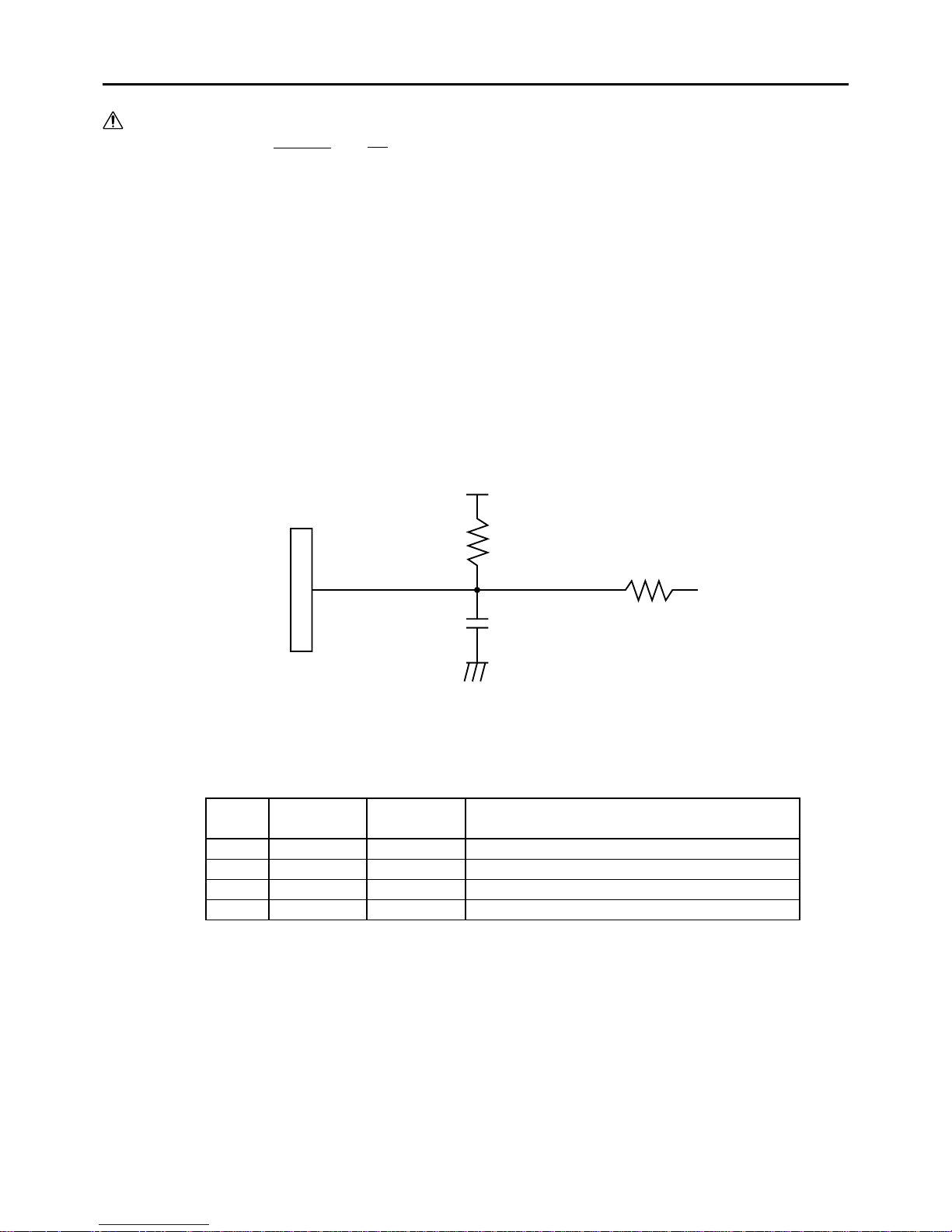
CAUTION:
1. For LED of ERROR and PE, there is a resister of 330Ω on the circuit side to make current
value 10 mA.
Please use LED which its voltage is approx. 2V. LED over 10 mA may break a control board.
2. Control circuit requires power supply only for one pin of each VCC and GND.
However, Operation voltage is to be supplied to all of pin for safety use.
3. Serial interface equips a driver and receiver of RS-232C, make sure to use it at RS-232C
level.
4. RESET terminal is pulled up by 3.3KΩ. Make sure to make this terminal NC, when this
terminal is not used.
5. LF-SW input circuit is as below.
3.4 CN4 Connector for Paper Cutter
1
2
3
4
M+
M–
GND
SW
Output
Output
––
Input
Function
Cutter motor operational signal M +
Cutter motor operational signal M –
GND
Cutter switch input signal
Pin No. Signal Name I/O
Using Connector : 5267- 04A-X (Molex)
Note: Use the specified Paper Cutter (Model Name : ACS-220-5V)
CN
VCC
47k
1000pF
1k
CPU
BD2-2880/2890 User’s Manual
7
4. DIP SWITCH SETTING
(1) DIP SWITCH
(2) JUMPER
(3) INTERFACE & BAUD RATE
DS1-1
1-2
1-3
1-4
1-5
1-6
1-7
1-8
Auto Cutter
CR Selection
Print Density
DTR/XON-XOFF
Baud Rate
"
"
"
Enable
LF Enable
XON-XOFF
Factory Setting
OFF
ON
OFF
OFF
OFF
OFF
OFF
OFF
OFF
Disable
LF Disable
DTR/DSR
Pin No. Function ON
Combination with J-6 (See next page (5))
See below (3)
J1
J2
J3
J4
J5
J6
J7
J8
International Character set
"
"
Paper Auto Loading
Print Drive System
Print Density
(Supplementary)
Not Used
Mechanism
Enable
Variable division
Factory Setting
Short circuit
Short circuit
Short circuit
Short circuit
Short circuit
Short circuit
Short circuit
Short circuit
Open
Disable
Fixed division
Pin No. Function Short
See next page (4)
Combination with DS1-3
See next page (5)
–
OFF
OFF
OFF
OFF
OFF
OFF
OFF
OFF
ON
ON
ON
ON
ON
ON
ON
ON
OFF
OFF
OFF
OFF
ON
ON
ON
ON
OFF
OFF
OFF
OFF
ON
ON
ON
ON
–
1200 bps
2400 bps
4800 bps
9600 bps
19200 bps
1200 bps
2400 bps
4800 bps
9600 bps
19200 bps
1200 bps
2400 bps
4800 bps
9600 bps
19200 bps
DS1-8 DS1-7
OFF
OFF
ON
ON
OFF
OFF
ON
ON
OFF
OFF
ON
ON
OFF
OFF
ON
ON
DS1-6
OFF
ON
OFF
ON
OFF
ON
OFF
ON
OFF
ON
OFF
ON
OFF
ON
OFF
ON
DS1-5
Parallel Input
Serial Input
"
"
"
"
"
"
"
"
"
"
"
"
"
"
Input Method
–
None
"
"
"
"
Odd
"
"
"
"
Even
"
"
"
"
Parity Baud Rate
MLT-288 MLT-289 *1
*1 : BD2-2890 is set to open circuit.
BD2-2880/2890 User’s Manual
8
Note:
1. Input Buffer is 2k byte. (Fixed)
2. Serial data length is 8 bits. (Fixed)
If print tone is set at 2 or above, printing rate tends to be lowered.
Open
Open
Open
Open
Short
Short
Short
Short
Open
Open
Short
Short
Open
Open
Short
Short
J-3 J-2
Open
Short
Open
Short
Open
Short
Open
Short
J-1
Japan (JIS)
Japan (Shift-JIS)
Sweden
Denmark 1
U.K.
Germany
France
U.S.A
InternationalCharacter
(4) INTERNATIONAL CHARACTER SET
(5) PRINT DENSITY
OFF
OFF
ON
ON
Open
Short
Open
Short
DS1-3 J-6
Light
Standard
Slightly Dark
Dark
Print Density
0
1
2
3
Level
80%
100%
120%
150%
Print Density Rate

BD2-2880/2890 User’s Manual
9
5. POWER SUPPLY
5.1 Specifications
VCC : 5V ±5% Approx. 130 mA
VP : 4.2V ~ 8.5V Approx. 1.5A (Peak : Approx. 4A) when 7.2V
Ordinal Voltage is to be 7.2V (Max). 8.5V is a voltage that is right after charging.
8.5V cannot be used for ordinal voltage.
5.2 Precautions
(1) Design the product to supply power to Vcc before VP when power is supplied to this control
board.
(2) Design the product to turn off the power for Vcc after VP when power is turned off.
(3) Make sure to turn off the power in case of connecting/disconnecting connectors.
(4) Make sure to use Vcc and VP following their specifications.
(5) Make sure to use this control board connecting all of terminals between VP and P-GND.

BD2-2880/2890 User’s Manual
10
6. PARALLEL INTERFACE
6.1 Specifications
Data input method : 8 bit parallel signal (DATA0~7)
Control signals : ACK, BUSY, STB, FAULT, PE, RESET
6.2 Explanation of Input/Output Signals
DATA0~7 : 8 bit parallel signal (Positive logic)
STB : Strobe signal to read 8 bit data (Negative logic)
RESET : Signal to reset control board (Negative logic)
ACK : 8 bit data request signal. Pulse signal output at the end of the BUSY
signal (Negative logic)
BUSY : Signal to indicate BUSY state of the printer. Input new data for “LOW”
(Positive logic)
FAULT : Signal which is made “LOW” when printer is in alarm state.
(Negative logic)
In this case all the control logics within the printer stop functioning.
PE : Signal which is output when paper runs out. (Positive logic)
6.3 Electrical Characteristics
(1) Input Signal Level
“HIGH” level : 0.7 Vcc MIN
“LOW” level : 0.3 Vcc MAX
(2) Output Signal Level
“HIGH” level : Vcc - 0.1V MIN
“LOW” level : 0.1V MAX

BD2-2880/2890 User’s Manual
11
[Printer side]
[Host side]
[Printer side]
[Host side]
All the output signals are pulled up by 50K
(3) I/O Conditions
STB, RESET input signals are pulled up by 3.3K .
Other input signals are pulled up by 50K .
VCC
TWIST PAIR WIRE
VCC
TWIST PAIR WIRE
6.4 Timing Chart
(1) Data Input and Printing Timing
T1, T2, T3 : 0.5 µs (MIN)
T4 : 270 ns (MAX)
T5 : 2.3 µs (TYP)
T6 : 500 ms (MIN) *On supplying power
SupplPower
DATA
STB
T6
T5
T1
T2
T3
T4
BUSY
BUSY
ACK
y

BD2-2880/2890 User’s Manual
12
6.5 Data Receiving Control
When BUSY signal is “LOW”, data from the host can be received. When it being “HIGH”, data
cannot be received.
6.6 Buffering
This control board incorporates 2K byte buffer.
Therefore, big data can be buffered in input buffer, and the host side can be released immediately.

BD2-2880/2890 User’s Manual
13
7. SERIAL INTERFACE
7.1 Specifications
(1) Data transfer system: Asynchronous
(2) Baud rates
1200, 2400, 4800, 9600, 19200 bps (Selectable by user)
(3) Configuration of one word
Start bit : 1 bit
Data bit : 8 bits Fixed
Parity bit : Odd/Even or No parity (Selectable by user)
Stop bit : 1 bit or more
(4) Signal polarity
RS-232C
• Mark = logic “ 1” (–3V ~ –12V)
• Space = logic “ 0” (+3V ~ +12V)
(5) Receiving data (RD signal)
RS-232C
• Mark = 1
• Space = 0
(6) Receiving control (DTR signal)
RS-232C
• Mark : Data transfer is not available
• Space : Data transfer is available
(7) Transmission control (TD signal)
DC1 code (11H) X-ON : Data reception is available
DC3 code (13H) X-OFF : Data reception is not available

BD2-2880/2890 User’s Manual
14
7.2 Explanation of Input/Output Signals
(1) RXD
Serial receiving data signal. On occurrence of framing error, overrun error, or parity error, the
data is printed as “?”.
(2) DTR
When this signal is READY, write data or a command. When they are written in BUSY, overrun
error is occurred and data is ignored. Data can be written into the input buffer even when the
printer is busy printing. A BUSY also occurs when the printer is powered on, in test print, in
Online mode, or being reset.
(3) TXD
If data remaining in the printer's input buffer is 256 bytes or less, the printer transfers a DC3
(13H: Data Receive Not Ready) signal to the host. If data in the input buffer exceeds 256 bytes,
the printer transfers a DC1 (11H: Data Receive Ready) signal to the host.
(4) GND
Common GND on the circuit.
7.3 Error Detection
Parity, framing, and overrun are detected. On detection of any error, the data are stored in the
buffer as “?”.
(1) Framing Error
With “space” state having been detected on detection of a stop bit, error takes place.
The data are stored in the buffer as “?”.
(2) Parity Error
With an error having been detected under specifying parity check, the data is stored in the buffer
as “?”.
(3) Overrun Error
On detection of an overrun error, the data are stored in the buffer as “?”.
7.4 Data Receiving Control
When DTR/DSR control having been selected, with BUSY signal at “LOW”, data from the host
side are received. With the signal at “HIGH”, they can not be received.
When DTR/DSR control not having been selected, after X-ON transmission, data is received
from the host side. No transmission of data can take place after X-OFF is transmitted.

BD2-2880/2890 User’s Manual
15
7.5 Buffering
Data transfer to the input buffer include DTR signals and TD signals as the control signals
concerned.
(1) DTR signals (See the page 7.2 (2))
(2) TXD signals (See the page 7.2 (3))
7.6 Electrical Characteristics
(1) RS-232C Circuit
Input (RXD, DSR)
<Printer side> <Host side>
Output (DTR, TXD)
<Printer side> <Host side>
Equivalent MAX232
Equivalent MAX232

BD2-2880/2890 User’s Manual
16
8. ERROR HANDLING
8.1 Peripheral Circuit Errors
These errors are detected at power-on or initialization just after a reset.
(1) Error types
(2) External signal outputs
(3) Resetting methods
8.2 Operation Errors
(1) Error types
Caution: The 8.5V upper-limit voltage for VP voltage error is only an assumptive voltage just
after charging the battery when using the battery power. It cannot be normally used. A
normal maximum voltage is 7.2V.
(2) External signal outputs
Memory error
Cutter error
Error
The CPU made a self-diagnosis of the circuit and detected an error with the external
RAM.
With the auto cutter enabled at the function selection terminal (DS1-1), the auto
cutter (ACS-220-5V) is not connected to the cutter connector (CN4).
Description
20
22
27
38
Pin No
ERROR
DTR
BUSY
FAULT
Signal Name
LED output. For a blinking pattern, see 8.3 Error Indication.
Serial interface
Parallel interface
Parallel interface
Remarks
Memory error
Cutter error
Error
Unrecoverable
After turning off the power, connect the auto cutter (ACS-220-5V) or turn off the
function selection terminal (DS1-1) and turn on the power again.
Resetting Method
No paper
Head –up
VH voltage error
Head temperature error
Cutter lock
(ACS-220-5V)
Error
The printing paper set is not set
The head-up lever is at its up position
A VH voltage is beyond its allowable range (4.2 to 8.5V)
A head temperature is less than 0˚C or 65 ˚C or higher.
When driving the cutter, the cutter is locked due to an external factor (Paper
jam, etc.).
Description

BD2-2880/2890 User’s Manual
17
(3) Resetting methods
Note 1. When auto loading has not been selected with the function selection jumper (J4), set the
paper manually. When it has been selected, the auto loading function is enabled to
facilitate replacement of the paper.
Note 2. The 8.5V upper-limit voltage for VP voltage error is only an assumptive voltage just
after charging the battery when using the battery power. It cannot be normally used. A
normal maximum voltage is 7.2V.
20
21
22
27
37
38
Pin No
ERROR
PE OUT
DTR
BUSY
PE
FAULT
Signal Name
LED output. For a blinking (Lighting) pattern, see 8.3 Error Indication.
LED output. This is always output at the time of no paper.
Serial interface
Parallel interface
Parallel interface
Parallel interface
Remarks
No paper
Head –up
VP voltage error
Head temperature
error
Cutter lock
(ACS-220-5V)
Error
Set the paper. See Note 1.
Bring down the head-up lever.
Set to a voltage within the allowable range (4.2 to 8.5V) and turn on the power
again. Alternatively, activate the Pin19 (LFSW) of the CN3(interface connector).
At the lower limit (less than 0 ˚C), printing becomes operational at 0 ˚C higher.
At the upper limit (65 ˚C or higher), it become operational at 60 ˚C or lower.
Eliminate paper jam and activate the Pin19(LFSW) of the CN3(Interface Connector)
or turn on the power again.
Resetting Method
Caution:

BD2-2880/2890 User’s Manual
18
Memory error
Cutter lock (Cutter error)
Head –up
VP voltage error
Head temperature error
Macro execution wait
Error
Blinking cycle of 200ms
Blinking cycle of 150ms(3 times)
and 500ms(1 time).
Illuminated until reverted
Illuminated until reverted
Blinking cycle of 1 sec.
Blinking cycle of 500ms.
DescriptionDisplay Pattern
8.3 Errors Indication
The errors other than no paper are indicated by a LED output (Illumination or blinking) of the
Pin 20 (ERROR) of the CN3 (Interface connector).

BD2-2880/2890 User’s Manual
19
9. PRINTER MECHANISM CONTROL SYSTEM
9.1 Thermal Head Control System (Division Driving System)
The MLT-288 (Line thermal printer) is driven by this control board has a384 dots/line head
divided into 6 blocks of 64 dots each. When actually driving the head, you can select either
Fixed Division Number system, which drives the head, always dividing it into 6 blocks or
Variable Division Number system which collectively drives several blocks at the time according
to the number of activated head dots.
For selection by function selection, see 4. DIP SWITCH SETTING.
For selection by a command, see 11. PRINT CONTROL FUNCTIONS.
9.1.1 Fixed Division Number System
This system always drives each block in the same sequence.
Note: for a stepping motor driving method, see 9.2 Motor Drive.
9.1.2 Variable Division Number System
This system counts the number of printing dots for each block of the printing dot line and drives
the blocks collective in such a manner not to exceed the maximum number of driving dots (64
dots).
1st Block
64 Dots
2nd Block
64 Dots
3rd Block
64 Dots
4th Block
64 Dots
5th Block
64 Dots
6th Block
64 Dots
1st Step of Motor
2nd Step of Motor
1 Dot Line
1st Block
64 Dots
2nd Block
64 Dots
3rd Block
64 Dots
4th Block
64 Dots
5th Block
64 Dots
6th Block
64 Dots
1 Dot Line
1st Step of Motor
2nd Step
1st Step of Motor
2nd Step of Motor

BD2-2880/2890 User’s Manual
20
9.2 Motor Drive
The MLT-288 uses a 4-phase bipolar stepping motor. It feeds the 1 dot line worth of paper in
two steps by 2-to-2 phase excitation.
9.2.1 Motor Drive Features
1) Drive at an optimum drive speed by the VP voltage.
2) Prevents heat generation of the motor by PWM control to restrain current consumption.
3) Provides acceleration control at the time of start.
9.2.2 Maximum Motor Drive Speeds at Major Voltage
Caution: The maximum drive speed depends on the VH voltage.
A printing speed may slightly differ depending on a processing time or voltage
detection accuracy. During the course of printing, a motor drive speed may be slower
than the maximum drive speed, depending on what is printed or the head divided drive
system.
5V
6V
7.2V
VH Voltage
400pps
600pps
840pps
Motor Drive Speed

BD2-2880/2890 User’s Manual
21
10. MAINTENANCE AND SERVICE
For the information on maintenance and service, please contact our dealer or at the following
address.
Northern America Other Areas
CBM America Corporation Japan CBM Corporation
Service Center Information Systems Division
363 Van Ness Way Suite 404 5-68-10, Nakano Nakano-ku,
Torrance, CA 90501, U.S.A Tokyo 164-0001 Japan
TEL 310-781-1460 TEL 03-5345-7540
FAX 310-781-9157 FAX 03-5345-7541
BD2-2880/2890 User’s Manual
22
11. PRINT CONTROL FUNCTIONS
11.1 Command List
Print Control Commands
Print Character Commands
Print Position Commands
Line Feed Span Commands
LF
CR
ESC J
ESC d
0Ah
0Dh
1Bh4Ah n
1Bh64h n
26
27
28
29
Control Code
Printing and paper feed
Print command
Printing and feeding paper n/203 inch
Printing and feeding the paper by n lines
Function Code Page
ESC SP
ESC !
ESC %
ESC &
ESC –
ESC E
ESC G
ESC R
ESC V
ESC t
ESC {
1Bh20h n
1Bh21h n
1Bh25h n
1Bh26h s n m
[ap1...ps×a]m–n+1
1Bh2Dh n
1Bh45h n
1Bh47h n
1Bh52h n
1Bh56h n
1Bh74h n
1Bh7Bh n
Control Code
Setting the right space amount of the character
Collective specifying printing mode
Specifying/canceling douwnload character set
Defining download characters
Specifying/canceling underline
Specifying/canceling highlighting
Specifying/canceling double printing
Selecting the international character set
Specifying/Canceling 90°-right- turned Characters
Selecting the character code table
Specifying/canceling the inverted characters
Function Code
30
31
33
34
36
37
38
39
40
41
42
Page
HT
ESC $
ESC D
ESC
ESC a
09h
1Bh24Ah n1 n2
1Bh44[n]k 00h
1Bh 5C n1 n2
1Bh 61h n
Control Code
Horizontal tab command
Specifying the absolute positions
Setting horizontal tab position
Specifying the relative positions
Aligning the characters
Function Code
43
44
45
46
47
Page
/
ESC 2
ESC 3
1Bh 32h
1Bh 33h n
Control Code
Specifying 1/6-inch line feed rate
Setting line feed rate of minimum pitch
Function Code
48
49
Page
BD2-2880/2890 User’s Manual
23
Bit Image Commands
Status Command
Panel Switch Command
Macro Commands
Cutter Commands
Bar Code Commands
ESC *
GS *
GS /
1Bh 2Ah m n1 n2[d]k
1Dh 2Ah n1 n2
1Dh 2F
Control Code
Specifying the bit image mode
Defining the download, bit image
Printing the download, bit image
Function Code
50
52
54
Page
ESC v 1Bh 76h
Control Code
Transmitting the printer status (Serial type)
Function Code
55
Page
ESC c5 1Bh 63h 35h n
Control Code
Enabling/disabling the panel switches
Function Code
56
Page
GS :
GS ^
1Bh 63h 35h n
1Dh 5Eh n1 n2 n3
Control Code
Starting/ending macro definition
Executing the macro
Function Code
59
58
Page
ESC i
ESC m
1Bh 69h
1Bh 6Dh
Control Code
Activating auto cutter (Full cut)
Activating auto cutter (Partial cut)
Function Code
59
60
Page
GS H
GS f
GS h
GS k
GS w
1Dh 48H n
1Dh 66H n
1Dh 68H n
1Dh 6Bh n[‘d’]k 00h
1Dh 77H n
Control Code
Selecting of print position of HRI code
Selecting the font of HRI code
Selecting the height of the bar code
Printing the bar code
Selecting the horizontal size (scale factor) of bar code
Function Code
61
62
63
64
68
Page

BD2-2880/2890 User’s Manual
24
ESC =
ESC @
DC2 A
1Bh 3Dh n
1Bh 40h
12h 41h n
Control Code
Data input control
Initializing the Printer
Selecting the Print drive system
Function Code
69
70
71
Page
Other Commands
NOP Commands
ESC c 3
ESC c 4
ESC p
ESC u
–
–
–
–
Control Code
NOP
NOP
NOP
NOP
Function Code
–
–
–
–
Page

BD2-2880/2890 User’s Manual
25
11.2 Command Details
11.2.1 Description of Items
XXXX ALL
Command Function
A sequence of code constituting a command is represented in hexadecimal number for <
>H, binary number for < >B, and decimal number for < >, respectively; [ ]k represents a
repeat count of k-times.
Describes an argument value(setting range) for the command.
Describes a command outline.
Describes a caution as required.
Describes an initial value for the command when accompanied by an argument.
Describes the associated commands for use.
Describes a coding example in the Q-BASIC sample program.
* This example is only for your reference and differs depending on the language
used, version, and so on. For details, see the ma
nual for the language used.
[Function]
[Code]
[Range]
[Outline]
[Caution]
[Default]
[See Also]
[Sample Program]
BD2-2880/2890 User’s Manual
26
LF
Printing and Paper Feed Command
<0A>H
Prints data inside the input buffer and feeds lines based on the line feed amount having been set.
• The head of the line becomes the next print starting position.
ESC 2, ESC 3
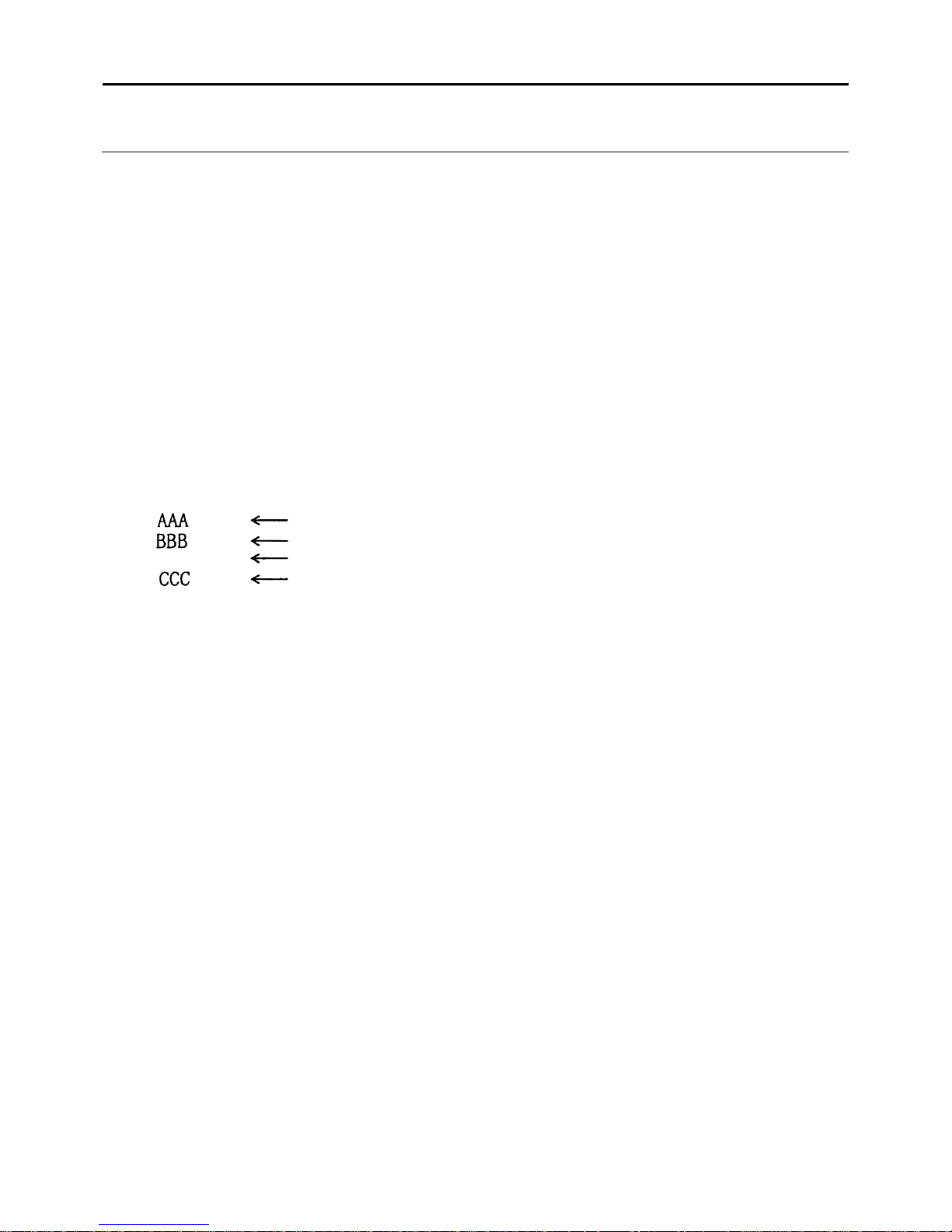
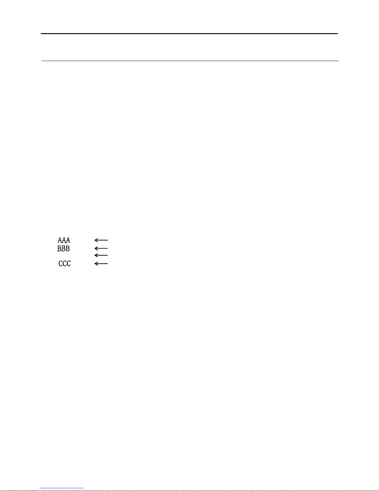
[Print Results]
LPRINT "AAA" + CHR$ (&HA);
LPRINT "BBB" + CHR$ (&HA);
LPRINT CHR$ (&HA);
LPRINT "CCC" + CHR$ (&HA
);
Print and line feed
Print and line feed
Line feed only
Print and line feed
[Function]
[Code]
[Outline]
[See Also]
[Sample Program]
BD2-2880/2890 User’s Manual
27
CR
Print Command
<0D>H
1) When DS 1-2 is OFF:
This command is ignored.
2) When DS 1- 2 is ON:
With data held inside the internal print buffer, printing and line feed are performed.
Without data inside the internal print buffer, however, no printing is performed.
LF
LPRINT "AAA" + CHR$ (&HD);
LPRINT "BBB" + CHR$ (&HD);
LPRINT CHR$ (&HD);
LPRINT "CCC" + CHR$
(&HD);
Print and line feed
Print and line feed
Line feed only
Print and line feed
[Function]
[Code]
[Outline]
[See Also]
[Sample Program]
[Print Results]

BD2-2880/2890 User’s Manual
28
ESC J n
Printing and feeding paper n/203 inch
<1B>H<4A>H<n>
{0 =< n =< FF} Data is described in Hex code.
Prints data inside the print buffer and feeds paper by n/360 inch. Since an actual mechanical
pitch is 1/203 inch, it is internally converted approximate to the value specified with this
command.
•
Specified volume does not remain.
•
The beginning of the line is to be considered as the next printing start position.
•
Initial value is not defined.
See Sample Program and Print Results for ESC 2 on Page
48.
[Function]
[Code]
[Range]
[Outline]
[Sample Program]
[Print Results]

BD2-2880/2890 User’s Manual
29
ESC d n
Printing and Feeding the paper by n lines
<1B>H<64>H<n>
* {0 =< n =< FF} Data is described in Hex code.
Prints data inside the buffer and feeds paper by n lines.
•
Specified line does not remain.
•
The beginning of the line is to be considered as the next printing start position.
•
The initial value is not defined.
LPRINT "AAAAA"
LPRINT CHR$ (&H1B) + "d" + CHR$ (2);
LPRINT "AAAAA" + CHR$ (&HA);
2/6-inch line feed
[Function]
[Code]
[Range]
[Outline]
[Default]
[Sample Program]
[Print Results]

BD2-2880/2890 User’s Manual
30
ESC SP n
Setting the right space amount of the character
<1B>H<20>H<n>
{0 =< n=< 20} Data is described in Hex code.
The rightward space amount is set in dot unit (1/203 inch unit). In the initial value, it is n=0.
The rightward space amount in doublewide mode is made double of the set volume.
n = 0
LPRINT CHR$ (&H1B) + " " + CHR$ (0);
LPRINT "AAAAA" + CHR$ (&HA);
LPRINT CHR$ (&H1B) + " " + CHR$ (1);
LPRINT "AAAAA" + CHR$ (&HA);
LPRINT CHR$ (&H1B) + " " + CHR$ (12);
LPRINT "AAAAA" + CHR$ (&HA);
0-dot space
1-dot space
12-dot space
[Function]
[Code]
[Range]
[Outline]
[Caution]
[Default]
[Sample Program]
[Print Results]

BD2-2880/2890 User’s Manual
31
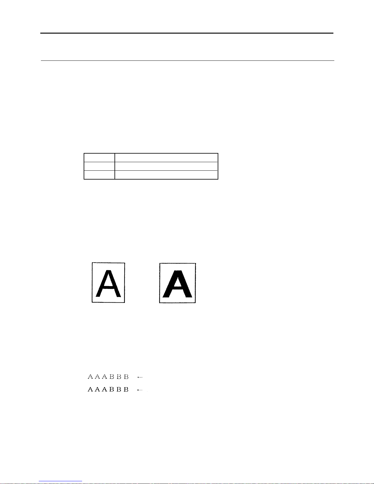
ESC ! n
Collective Specifying Printing Mode
<1B>H<21>H<n>
{0 =< n=< FF} Data is described in Hex code.
Printing mode is assigned. Each n bit indicates the following:
Va l ue
Bit Function 0 1
0 Character Font Font A Font B
1 Undefined
2 Undefined
3 High-lighting Canceled Specified
4 Double height Canceled Specified
5 Double width Canceled Specified
6 Undefined
7 Underline Canceled Specified
• With double height and double width being specified simultaneously, double wide and
double high characters are consisted.
• An underline is attached to the full character width, which, however, is not attached to
the part having been skipped by the horizontal tab.
Neither is it attached to 90°-right-turned characters.
• The underline width is as having been specified by <ESC ->.
(The default setting is 1 dot width. )
• Specification with this command is invalid to Kanji, except specification and cancellation
of highlighting
• In case that double wide character and normal character exist in same one line, the layout
of underline is consistent one.
n = 0
ESC E,ESC
–
[Function]
[Code]
[Range]
[Outline]
[Caution]
[Default]
[See Also]

BD2-2880/2890 User’s Manual
32
LPRINT CHR$ (&H1B) + " ! " + CHR$ (&H00) + "H" ;
LPRINT CHR$ (&H1B) + " ! " + CHR$ (&H01) + "H";
LPRINT CHR$ (&H1B) + " ! " + CHR$ (&H08) + "H";
LPRINT CHR$ (&H1B) + " ! " + CHR$ (&H10) + "H";
LPRINT CHR$ (&H1B) + " ! " + CHR$ (&H20) + "H";
LPRINT CHR$ (&H1B) + " ! " + CHR$ (&H80) + "H";
LPRINT CHR$ (&H1B) + " ! " + CHR$ (&HB9) + "H";
LPRINT CHR$ (&HA);
Font A
Font B
Font A + Highlighting
Font B + Highlighting + Quadruple + Underline
Font A + Underline
Font A + Double Width
Font A + Double Height
[Sample Program]
[Print Results]
BD2-2880/2890 User’s Manual
33
ESC % n
Specifying/Canceling Download Character Set
<1B>H<25>H<n>
{0 =< n =< FF} data is described in Hex code.
Specifying/canceling download characters.
Further, only the lowest bit (n0) is valid for n.
The lowest bit (n0) indicates the following.
n0 Function
0 Canceling download character set
1 Specifying download character set
Download characters and download bit images cannot be defined simultaneously.
n = 0
ESC &
GOSUB SETCHR DATA 6
LPRINT CHR$ (&H1B) + "%" + CHR$ (0); DATA &HFF, &H80, &H00
LPRINT "@A" + CHR$ (&HA); DATA &H80, &H80, &H00
LPRINT CHR$ (&H1B) + "%" + CHR$ (1); DATA &H80, &H80, &H00
LPRINT "@A" + CHR$ (&HA); DATA &H80, &H80, &H00
END DATA &HFF, &HFF, &HFF
SETCHR: DATA &HFF, &HFF, &HFF
LPRINT CHR$ (&H1B) + "&”; DATA 12
LPRINT CHR$ (3) + "@" + "A”; DATA &HFF, &HFF, &HFF
FOR J=1 TO 2 DATA &H80, &H07, &HF9
READ REP DATA &H80, &HFF, &HF9
LPRINT CHR$ (REP); DATA &H87, &HFE, &H01
FOR I=1 TO REP*3 DATA &H9F, &H06, &H01
READ D DATA &HF8, &H06, &H01
LPRINTCHR$ (D); DATA &HF8, &H06, &H01
NEXT I DATA &H9F, &H06, &H01
NEXT J DATA &H87, &HFE, &H01
RETURN DATA &H80, &HFF, &HF9
DATA &H80, &H07, &HF9
DATA &HFF, &HFF, &HFF
Internal Character Set
Download Character
[Function]
[Code]
[Range]
[Outline]
[Caution]
[Default]
[See Also]
[Sample Program]
[Print Results]

BD2-2880/2890 User’s Manual
34
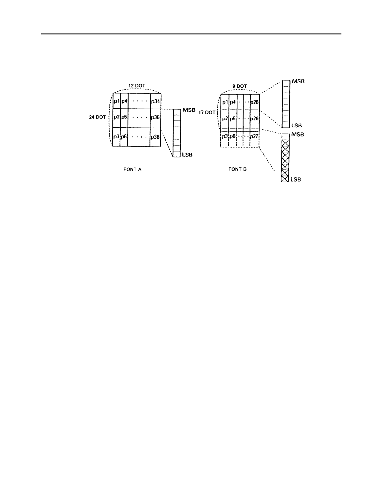
ESC & s n m [a [p] s a] m – n +1
Defining Download Character
<1B>H<26>H<s><n><m> [<a><p1><p2><ps a>]m-n+1
{s = 03}
{20 (Hex) =< n =< m =< 7E (Hex)}
{0 =< a =< 0C(Hex)} (Font A)
{0 =< a =< 0A(Hex)} (Font B)
Defines the font of download characters of alphanumeric characters.
• "s" indicates the number of bytes in vertical direction.
• "n" indicates the start character code and m the end character code. To define only one character,
set n=m.
• Character codes definable includes 95 ASCII codes in total between <20>H~<7E>H.
• "a" indicates the number of dots in horizontal direction for definition.
• "p" is the data to be defined, which indicate a pattern equal to "a" dot in horizontal direction from
the left end. The rest of the pattern on the right side is filled with space.
The rest of data to be defined is s x a.
• Download characters thus defined remain valid until redefinition, ESC @ execution,
GS * execution, or power OFF is practiced.
Download characters and download bit images can not be defined simultaneously.
Running this command clears the definition of the download bit image.
Same
as the internal character set
×
×
[Function]
[Code]
[Range]
[Outline]
[Caution]
[Default]
BD2-2880/2890 User’s Manual
35
[Example]
Create each data bit by setting "1" for a printed dot and "0" for an unprinted dot.
[Print Results]
See Sample Program and Print Results for ESC % on Pa
ge 33.
[Sample Program]

BD2-2880/2890 User’s Manual
36
ESC – n
Specifying/ Canceling Underline
<1B>H<2D>H<n>
{0 =< n =< 02} data is described in Hex code.
Specifying/canceling an underline.
• Types of underlines by n value are shown below:
n (Hex) Type
0 Canceling an underline.
1 Specifying an underline for 1-dot width.
2 Specifying an underline for 2-dots width.
• An underline is attached to the full character width. It is, however, not attached to
the part having been skipped by horizontal tab command.
• An underline is not attached to a 90 °- right-turned characters.
• Specification/cancellation with this command is invalid to Kanji.
ESC !, FS
–
LPRINT CHR$ (&H1B) + "–" + CHR$ (0);
LPRINT "AAAAA" ;
LPRINT CHR$ (&H1B) + "
–
" + CHR$ (1);
LPRINT "AAAAA" + CHR$ (&HA);
[Print Re
sults]
Underline Canceled
Underline Specified
[Function]
[Code]
[Range]
[Outline]
[Caution]
[See Also]
[Sample Program]
BD2-2880/2890 User’s Manual
37
ESC E n
Specifying/canceling highlighting
<1B>H<45>H<n>
{0 =< n =<FF} Data is described in Hex code.
Specifying/canceling the highlighting characters.
•
"n" is valid only for the lowest bit (n0).
•
Control by the lowest bit (n0) is shown as follows:
n0 Type
0 Canceling highlighting.
1 Specifying highlighting.
•
This is effective to all characters.
•
Dot configuration of a highlighted character includes one extra dot added at its side.
•
The print result of Double printing and highlight character printing is completely same.
ESC !
[Example]
LPRINT CHR$ (&H1B) + "E" + CHR$ (0);
LPRINT "AAABBB" + CHR$ (&HA);
LPRINT CHR$ (&H1B) + "E" + CHR$ (1);
LPRINT "AAABBB" + CHR$ (&HA);
Highlighting canceled
Highlighting canceled
[Function]
[Code]
[Range]
[Outline]
[Caution]
[See Also]
[Sample Program]
[Print Results]

BD2-2880/2890 User’s Manual
38
ESC G n
Specifying/canceling Double Printing
<1B>H<47>H<n>
{0 =< n =< FF} Data is described in Hex code.
Specifying/canceling the double printing.
•
"n" is valid only for the lowest bit (n0).
•
Control by n is shown as follows.
n0 Type
0 Canceling double printing.
1 Specifying double printing.
•
This is effective to all characters.
•
The print result of Double printing and highlight character printing is completely same.
ESC E
LPRINT CHR$ (&H1B) + "G" + CHR$ (0);
LPRINT "AAABBB" + CHR$ (&HA);
LPRINT CHR$ (&H1B) + "G" + CHR$ (1);
LPRINT "AAABBB" + CHR$ (&HA);
Highlighting canceled
Highlighting canceled
[Function]
[Code]
[Range]
[Outline]
[Caution]
[See Also]
[Sample Program]
[Print Results]
BD2-2880/2890 User’s Manual
39
ESC R n
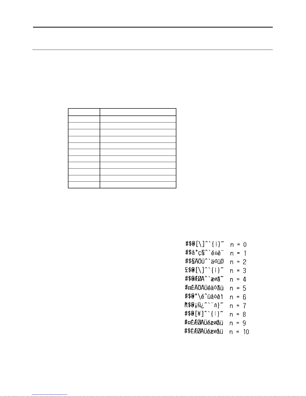
Selecting the International Character set
<1B>H<52>H<n>
{0 =< n =< 0A) Data is described in Hex code.
Depending on the value of n, following character sets are specified.
n(Hex) Character Set
0 U.S.A.
1 France
2 Germany
3 U.K.
4 DenmarkI
5 Sweden
6 Italy
7 Spain
8 Japan
9 Norway
A DenmarkII
•
The initial value of n indicates the character set specified by Jumper (J1~J3).
Character Code Table (International Character Set)
FOR I=0 TO 10
LPRINT CHR$ (&H1B) + "R" + CHR$ (I);
LPRINT " #$@[¥]^”;
LPRINT CHR$ (&H60) + "{¥} ˜";
LPRINT "n=" + STR$ (I);
LPRINT CHR$ (&HA);
NEXT
I
[Function]
[Code]
[Range]
[Outline]
[Default]
[See Also]
[Sample Program]
[Print Results]

BD2-2880/2890 User’s Manual
40
ESC V n
Specifying/Canceling 90°-right- turned Characters
<1B>H<56>H<n>
{0 =< n =< 1} Data is described in Hex code.
Specifying/canceling characters 90°-right- turned character.
•
"n" means the followings.
n (Hex) Condition
0
Canceling
90°-right- turned Characters
1
Specifying
90°-right- turned Characters
•
No underlines are attached to 90°-right- turned characters.
•
The initial value of n is "0".
LPRINT CHR$ (&H1B) + "V" + CHR$ (0);
LPRINT "AAAAA”;
LPRINT CHR$ (&H1B) + "V" + CHR$ (1);
LPRINT "AAAAA" + CHR$ (&HA);
90° Rotation Canceled
90° Rotation Specified
[Function]
[Code]
[Range]
[Outline]
[Caution]
[Default]
[Sample Program]
[Print Results]

BD2-2880/2890 User’s Manual
41
ESC t n
Selecting Character Code Table
<1B>H<74>H<n>
{0 =< n =< 1} Data is described in Hex code.
Selecting Page n on the character code table:
The character code table is selected depending on the value of n.
"n" means the followings.
n (Hex) Condition
0 Page0(IBM Character #2)
1 Page1(Domestic Character)
The initial value of n is subject to the character set for the country specified
by the Jumper(J1~J3).
•
When Japan is selected: Domestic characters
•
When non-Japan is selected: IBM characters #2
Character Code Table
LPRINT CHR$ (&H1B) + "t" + CHR$ (0);
LPRINT " n=0 “;
FOR C=&HB1 TO &HB5
LPRINT CHR$ (C);
NEXT C
LPRINT CHR$ (&HA);
LPRINT CHR$ (&H1B) + "t" + CHR$ (1);
LPRINT " n=1 “;
FOR C=&HB1 TO &HB5
LPRINT CHR$ (C);
NEXT C
LPRINT CHR$ (&HA);
Page 0
Page 1
[Function]
[Code]
[Range]
[Default]
[See Also]
[Sample Program]
[Print Results]

BD2-2880/2890 User’s Manual
42
ESC { n
Specifying/Canceling the Inverted Characters
<1B>H<7B>H<n>
{0 =< n =< FF} Data is described in Hex code.
Specifying/canceling inverted characters.
•
"n" is valid only for the lowest bit (n0).
•
Bit n (n0) means the followings.
n0 Condition
0 Canceling inv rted characters.
1 Specifying inverted characters.
•
Inverted-printing means printing the line at 180°turned.
•
This is valid only when this is specified at the beginning of a line.
•
The initial value of n is "0".
LPRINT CHR$ (&H1B) + "{" + CHR$ (0);
LPRINT "AAAAA" + CHR$ (&HA);
LPRINT "BBBBB" + CHR$ (&HA);
LPRINT CHR$ (&H1B) + "{" + CHR$ (1);
LPRINT "AAAAA" + CHR$ (&HA);
LPRINT "BBBBB" + CHR$ (&HA);
Inversion Canceled
Inversion Specified
Paper Feed Direction
[Function]
[Code]
[Range]
[Outline]
[Caution]
[Default]
[Sample Program]
[Print Results]

BD2-2880/2890 User’s Manual
43
HT
Horizontal Tab Command
<09>H
Shifts the printing position to the next horizontal tab position.
• Ignored when the next horizontal tab position has not been set.
• The horizontal tab position is set by ESC D.
• Initial setting of the horizontal tab position is each 8 characters in 9th, 17th,
25th,columns.
ESC D
LPRINT "0123456789012345678901”;
LPRINT CHR$ (&HA);
LPRINT CHR$ (&H9) + "AAA”;
LPRINT CHR$ (&H9) + "BBB”;
LPRINT CHR$ (&HA);
LPRINT CHR$ (&H1B) + "D”;
LPRINT CHR$ (3) + CHR$ (7) + CHR$ (14) + CHR$ (0);
LPRINT CHR$ (&H9) + "AAA”;
LPRINT CHR$ (&H9) + "BBB”;
LPRINT CHR$ (&H9) + "CCC" + CHR$ (&HA);
Initially set horizontal tab
When set to the 4th, 8th, and 15th digits
[Function]
[Code]
[Outline]
[Caution]
[See Also]
[Sample Program]
[Print Results]

BD2-2880/2890 User’s Manual
44
ESC $ n1 n2
Specifying the Absolute Positions
<1B>H<24>H<n1><n2>
{0 =< n1 =< FF}
{0 =< n2 =< 1} Data is described in Hex code.
The printing start position is specified in the number of dots (1/203 inch unit) from
the beginning of line.
•
The number of dots is divided by 256, whose quotient is taken as n2 and the residual as n1.
•
Therefore, the printing start position is equal to n1+n2 x 256 from the beginning of line.
•
Specifying beyond the line end is ignored.
•
The initial value is not specified.
ESC \
LPRINT CHR$ (&H1B) + "$”;
LPRINT CHR$ (0) + CHR$ (0) + "A”;
LPRINT CHR$ (&H1B) + "$”;
LPRINT CHR$ (50) + CHR$ (0) + "B”;
LPRINT CHR$ (&H1B) + "$”;
LPRINT CHR$ (0) + CHR$ (1) + "C”;
LPRINT CHR$ (&HA);
LPRINT CHR$ (&H1B) + "$”;
LPRINT CHR$ (100) + CHR$ (0) + "A”;
LPRINT CHR$ (&H1B) + "¥”;
LPRINT CHR$ (&HC2) + CHR$ (&HFF) + "B”;
LPRINT CHR$ (&HA);
Absolute Position Specified
Relative Position Specified – 62
[Function]
[Code]
[Range]
[Outline]
[Caution]
[Default]
[See Also]
[Sample Program]
[Print Results]

BD2-2880/2890 User’s Manual
45
ESC D [ n ] k NUL
Setting Horizontal Tab Position
<1B>H<44>H [ <n> ] k<00>H
{0 =< n =< FFH} Data is described in Hex code.
{0 =< k =< 20H} Data is described in Hex code.
Specifying a horizontal tab position.
•
"n" indicates the no. of columns from the beginning to the horizontal tab position.
At this time, n= set position
–
1 is to be specified. For example, to set the position at 9th
column, n=8 is to be specified.
•
k denotes the number of horizontal tab positions you want to set.
•
The tab position is set at position where it is "character width x n" from the line beginning.
The character width, at this time, includes the rightward space amount.
In double wide characters, it is made double of the ordinary case.
•
Tab positions can be specified are maximum 32. Specifying exceeding this is ignored.
•
<n> k, which denotes a setting position, is input in the increasing order and ends at <00> H.
•
ESC D NUL clears all the set tab positions. Following clearing, horizontal tab command is
ignored.
When the data, <n> k, is equal to or smaller than its preceding data, <n> k-1, it is assumed
that tab setting is finished. If this is the case, the next data onward will be processed as normal
data.
When the data, <n> k, exceeds a 1-line print area, set the horizontal tab position, assuming
"Set digit position = Maximum print digits + 1." The horizontal tab position does not
change even if the character width is altered after setting the horizontal tab position.
•
Initial value is specified for each eight characters(9th.17th.25th column) of ANK characters.
HT
See Sample Program and Print Results for HT on Page
43.
[Function]
[Code]
[Range]
[Outline]
[Caution]
[Default]
[See Also]
[Sample Program]
[Print Results]

BD2-2880/2890 User’s Manual
46
ESC n1 n2
Specifying the Relative Positions
<1B>H<5C>H<n1>< n2>
{0 =< n1 =< FF}
{0 =< n2 =< FF} Data is described in Hex code.
The printing start position is specified in the number of dots(1/203 inch unit) from
the current position.
•
Rightward direction is taken as plus and leftward direction as minus.
•
To specify N dot in minus (left) direction, use a complement of N for assignment.
–
N dots = 65536 – N
•
The number of dots is divided by 256, whose quotient is taken as n2 and the residual as n1.
•
Specifying exceeding the top of line or the end of line is ignored.
•
The initial value is not specified.
ESC $
See Sample Program and Print Results for ESC $ on Page
44.
\
[Function]
[Code]
[Range]
[Outline]
[Caution]
[Default]
[See Also]
[Sample Program]
[Print Results]

BD2-2880/2890 User’s Manual
47
ESC a n
Aligning the characters
<1B>H<61>H<n>
{0 =< n =< 2} Data is described in Hex code.
All the printed data within one line are aligned in the specified position.
•
Depending on n value, positional alignment is carried out as in the table below:
n (Hex) Position
0 Left end alignment
1 Centering
2 Right end alignment
•
This is valid only when n is inputted at the beginning of line.
•
The initial value of n is "0".
LPRINT CHR$ (&H1B) + "a" + CHR$ (0);
LPRINT "AAAAA" + CHR$ (&HA);
LPRINT CHR$ (&H1B) + "a" + CHR$ (1);
LPRINT "AAAAA" + CHR$ (&HA);
LPRINT CHR$ (&H1B) + "a" + CHR$ (2);
LPRINT "AAAAA" + CHR$ (&HA);
Left-justified Centered Right-justified
Paper Feed Direction
[Function]
[Code]
[Range]
[Outline]
[Caution]
[Sample Program]
[Print Results]

BD2-2880/2890 User’s Manual
48
ESC 2
Specifying 1/6-inch line feed rate
[Code] <1B>H<32>H
The line feed rate per line is specified by 1/6 inch.
LPRINT "AAAAA" + CHR$ (&HA);
LPRINT CHR$ (&H1B) + "3" + CHR$ (0);
LPRINT "AAAAA" + CHR$ (&HA);
LPRINT CHR$ (&H1B) + "3" + CHR$ (50);
LPRINT "AAAAA" + CHR$ (&HA);
LPRINT CHR$ (&H1B) + "2”;
LPRINT "AAAAA" + CHR$ (&HA);
LPRINT "AAAAA”;
LPRINT CHR$ (&H1B) + "J" + CHR$ (100);
LPRINT "AAAAA" + CHR$ (&HA);
LPRINT "AAAAA" + CHR$ (&HA);
1/6-inch line feed
0/360-inch line feed
50/360-inch line feed
1/6-inch line feed
100/360-inch line feed
1/6-inch line feed
[Function]
[Code]
[Outline]
[Sample Program]
[Print Results]

BD2-2880/2890 User’s Manual
49
ESC 3 n
Setting line feed rate of minimum pitch
<1B>H<33>H<n>
{0 =< n =< FF} Data is described in Hex code.
The line feed rate per line is specified by n/360 inch.
Since an actual mechanical pitch is 1/203 inch, it is internally converted approximate
to the value specified with this command.
• The initial value is n = 60 (1/6 inch) (18H), being 4.23 mm line feed rate.
See Sample Program and Print Results for ESC 2 on Pa
ge 48.
[Function]
[Code]
[Range]
[Outline]
[Default]
[Sample Program]
[Print Results]

BD2-2880/2890 User’s Manual
50
ESC * m n1 n2 [ d ] k
Specifying the Bit Image Mode
<1B>H<2A>H<m><n1><n2> [ <d> ] k
{m= 0, 1, 32, 33 bit image mode (See the table below.)}
{0 =< n1 =< FF(Hex)}
{0 =< n2 =< 03(Hex)}
{0 =< d =< FF(Hex)}
{k = n1 + FF(Hex) n2 (m = 0, 1)
{k = (n1+ FF(Hex) n2) 3} (m = 32, 33)
According to the number of dots specified in n1, n2, specify the bit image of mode n.
• The No. of dots printed is divided by 256, whose quotient is taken as n2 and residual as n1.
• The total no. of dots printed in the bit image is equal to n1 + (256 x n2).
• When bit image data have been input in excess of dot position of one line (448 dots) ,
the excess data are discarded.
• d is bit image data, the bits subject to printing are taken as "1" and those not as "0".
• The bit image modes specified by m are shown as follows:
Vertical Direction Horizontal Direction
m(Hex) Mode
No. of Dots Dot Density Dot Density Max. No. of Dots
0 8-dot single density 8 67 DPI 101 DPI 192
1 8-dot double density 8 67 DPI 203 DPI 384
32 24-dot single density 24 203 DPI 101 DPI 192
33 24-dot double density 24 203 DPI 203 DPI 384
• When the values set in m (bit image mode) are out of the above range, the data
following after n1 is processed as normal printing data.
• After completion of bit image printing, printer returns to normal data processing mode.
[Examp
le]
×
××
Single Density Double Density Single Density Double Density
[Function]
[Code]
[Range]
[Outline]
[Caution]

BD2-2880/2890 User’s Manual
51
[Sample Program]
LPRINT CHR$ (&H1B) + "*”;
LPRINT CHR$ (0) + CHR$ (20) + CHR$ (0); IMG1 :
GOSUB IMG1 LPRINT CHR$ (&HFF) ;
LPRINT CHR$ (&HA); FOR I=1 TO 18
LPRINT CHR$ (&H1B) + "*”; LPRINT CHR$ (&H85) ;
LPRINT CHR$ (1) + CHR$ (20) + CHR$ (0); NEXT I
GOSUB IMG1 LPRINT CHR$ (&HFF) ;
LPRINT CHR$ (&HA); RETURN
LPRINT CHR$ (&H1B) + "*”; IMG2 ;
LPRINT CHR$ (32) + CHR$ (20) + CHR$ (0); LPRINT CHR$ (&HFF) ;
GOSUB IMG2 LPRINT CHR$ (&HFF) ;
LPRINT CHR$ (&HA); LPRINT CHR$ (&HFF) ;
LPRINT CHR$ (&H1B) + "*”; FOR I=1 TO 18
LPRINT CHR$ (33) + CHR$ (20) + CHR$ (0); LPRINTCHR$ (&H80) ;
GOSUB IMG2 LPRINTCHR$ (&H00) ;
LPRINT CHR& (&HA); LPRINTCHR$ (&H05) ;
END NEXT I
LPRINT CHR$ (&HFF) ;
LPRINT CHR$ (&HFF) ;
LPRINT CHR$ (&HFF) ;
RETURN
[Print Results]

BD2-2880/2890 User’s Manual
52
GS * n1 n2 [ d ] n1 n2 8
Defining the Download Bit Image
<1D>H<2A>H<n1><n2> [ < d > ] n1 n2 8
{1 =< n1 =< FF}
{1 =< n2 =< 30}
{n1 n2 =< 51F} Data is described in Hex code.
Defines downloading bit images of the number of dots specified by n1/n2.
•
The numbers of dots are n1 x 8 in horizontal direction and n2 x 8 in vertical direction.
•
d indicates bit image data.
•
The download bit image thus defined remains effective until redefinition,
ESC @ execution, ESC &, or power OFF takes place.
•
A download character and a download bit image can not be defined simultaneously.
With this command executed, defined content of a download character is cleared.
•
Relations between the bit image data and the dot defined are shown below:
GS
/
××
××
If a download bit image is defined with this command while it is being printed (GS/) ,
printing operation may become unstable (fluctuating print pitch).
•
[Function]
[Code]
[Range]
[Outline]
[Caution]
[See Also]
BD2-2880/2890 User’s Manual
53
GOSUB IMG
LPRINT CHR$ (&H1D) + "/" + CHR$ (0);
LPRINT CHR$ (&H1D) + "/" + CHR$ (1);
LPRINT CHR$ (&H1D) + "/" + CHR$ (2);
LPRINT CHR$ (&H1D) + "/" + CHR$ (3);
END
IMG:
n 1 = 10 : n 2= 5
LPRINT CHR$ (&H1D) + "*”;
LPRINT CHR$ (n1) + CHR$ (n2);
FOR J=1 TO n1*8
FOR I=1 TO n2
LPRINT CHR$ (J);
NEXT I
NEXT J
RETURN
Nomal Mode
Double Width Mode
Double Height Mode
Quadruple Mode
[Sample Program]
[Print Results]
BD2-2880/2890 User’s Manual
54
GS / m
Printing the Download, Bit Image
<1D>H<2F>H<m>
{0 =< m =< 03} Data is described in Hex code.
Prints download bit image in a mode specified by m.
•
Modes can be selected by m are shown below.
m Mode Name Dot Density in
Vertical Direction
Dot Density in
Horizontal Direction
0 Normal mode 203 DPI 203 DPI
1 Double wide mode 203 DPI 101 DPI
2 Double high mode 101 DPI 203 DPI
3 Double wide/double high mode 101 DPI 101 DPI
•
When data exist inside the print buffer, this command is ignored.
•
When a download bit image has not been defined, this command is ignored.
•
A portion of a download bit image exceeding one line length is not printed.
•
A download character and a download bit image cannot be defined simultaneously.
•
The initial value is not specified.
GS *
See Sample Program and Print Results for GS * on Page
52.
If a download bit image data is defined while it is being printed with this command,
printing operation may become unstable (fluctuating print pitch).
•
[Function]
[Code]
[Range]
[Outline]
[Caution]
[Default]
[See Also]
[Sample Program]
[Print Results]
BD2-2880/2890 User’s Manual
55
ESC v (Serial Interface Only)
Transmitting the printer status (Serial Type)
<1B>H<76>H
Current printer status is transmitted.
•
Status sent out consists of 1 byte whose content is as in the table below.
•
In DTR/DSR control, after revertible state of the host (DSR signal being in SPACE
state) is confirmed, only 1 byte is transmitted. In XON/XOFF control, DSR signal state
not being confirmed, only 1 byte is transmitted.
•
In DTR/DSR control, when the host is in unrespectable state (DSR signal being in
MARK state), it waits until receptacle state is created.
•
In paper end (paper near end) status, this command may be unrespectable state due to
BUSY state.
Remarks. This command is valid only for serial interface model.
Va l u e Bit Function
0 1
0 Not defined
1 Not defined
2 Paper end With paper Without paper
3 Not defined
4 Not used Fixed to 0
–
5 Not defined
6 Not defined
7 Not defined
OPEN "COM1: N81NN" AS #1;
PRINT #1, CHR$ (&H1B) + "v”;
A$ = INPUT$ (1, #1);
CLOS
E #1
[Function]
[Code]
[Outline]
[Caution]
[Sample Program]

BD2-2880/2890 User’s Manual
56
ESC c5 n
Enabling/Disabling Panel Switches
<1B>H<63>H<35>H<n>
{0 =< n =< FF} Data is described in Hex code.
Selecting the LF switch valid/invalid.
•
"n" is valid only in the lowest bit (n0).
•
"n" bit means the followings.
n0
Condition
0 LFSW valid.
1 LFSW invalid.
When the panel switch is disabled with this command, the LF switch is disabled. Therefore,
the paper cannot be fed by operating the LF switch.
•
The initial value of n is "0".
LPRINT CHR$ (&H1B) + "c5" + CHR$ (0);
………
When enabling the LF switch
LPRINT CHR$ (&H1B) + "c5" + CHR$ (1);
………
When disabling the LF switch
[Function]
[Code]
[Range]
[Outline]
[Caution]
[Default]
[Sample Program]

BD2-2880/2890 User’s Manual
57
GS :
Starting / Ending Macro Definition
<1D>H<3A>H
Specifying starting / ending macro definition.
Means termination when received while defining a macro.
Maximum content available for macro definition is 2048 bytes.
A portion exceeding 2048 bytes is not defined.
•
Even with ESC @ (initialization of the printer) having been executed, defined content is not
cleared. Therefore, it is possible to include ESC @ into the content of macro definition.
•
Normal printing operation is carried out even while in macro definition
•
Initially, Macro is not specified.
GS ^
LPRINT CHR$ (&H1D) + “: " ;
LPRINT "+
–––
+" + CHR$ (&HA);
LPRINT " | | " + CHR$ (&HA);
LPRINT "+
–––
+" + CHR$ (&HA);
LPRINT CHR$ (&H1D) + “: “;
LPRINT CHR$ (&H1D) + " ^ “;
LPRINT CHR$ (2) + CHR$ (10);
LPRINT CHR$ (0);
Nomal Printing during
Macro Definition
Printing during Macro Execution
[Function]
[Code]
[Outline]
[Caution]
[Default]
[See Also]
[Sample Program]
[Print Results]

BD2-2880/2890 User’s Manual
58
GS ^ n1 n2 n3
Executing the Macro
<1D>H<5E>H<n1><n2><n3>
{0 =< n1 =< FF}
{0 =< n2 =< FF}
{0 =< 3 =< 1} Data is described in Hex code.
Executing contents defined in macro.
•
"n1~ n3" indicate as follows:
n1 : The number of times of macro execution
n2 : Waiting time on macro execution
Waiting time of n2 x 100msec is given for every execution.
n3 : Macro execution mode
n3 Mode
0 Continuous execution
1 Execution by LFSW
Continuous execution: The Macro is executed n1 times continuously at the time
intervals specified by n2.
Execution by FEED S: After waiting for lapse of time specified by n2, the ALAME
LED flickers and the LF switch is waited to be pressed. When
it is pressed, the macro is executed once.
This action is repeated n1 times.
•
When this command is received while in macro definition, suspension of macro definition is
indicated. At this time, the defined content is cleared.
•
No execution takes place when macro is held undefined or n1=0.
•
While in macro execution with n3=1, paper feed with the LF SW is not available.
•
Initially, this command is not specified.
GS :
See Sample Program and Print Results for GS : on Page
57.
[Function]
[Code]
[Range]
[Outline]
[Caution]
[Default]
[See Also]
[Sample Program]
[Print Results]
BD2-2880/2890 User’s Manual
59
ESC i (When Using Auto Paper Cutter)
Full Cut
<1B>H<69>H
Activating auto cutter unit (Full cut)
•
This is valid only when n is inputted at the beginning of line.
•
Prior to cutting the paper, feed the paper from the printing position to beyond the
paper cutting position of the cutter. Otherwise, the character just after print will
remain on this side of the cutter.
LPRINT "AAAAA”;
LPRINT CHR$ (&H1B) + "J”;
LPRINT CHR$ (150);
LPRINT CHR$ (&H1B) + "i”;
LPRINT "AAAAA”;
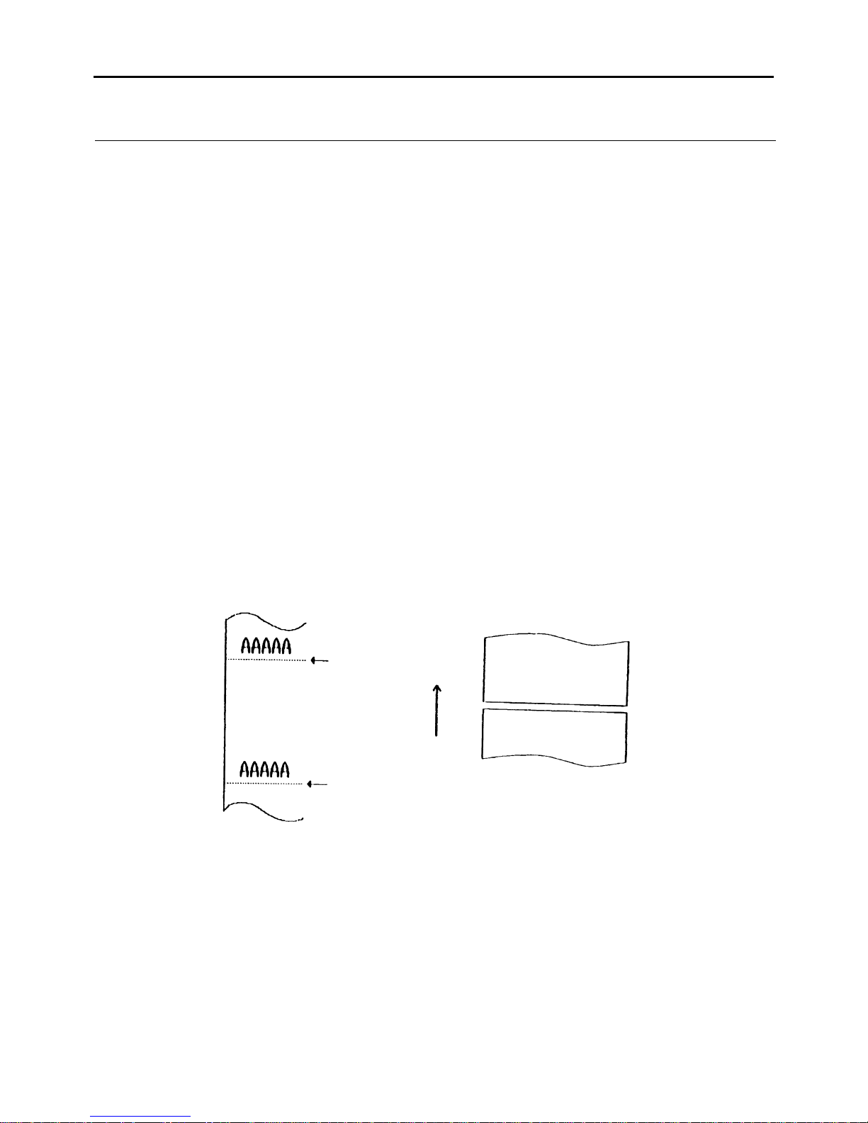
LPRINT CHR$ (&H1B) + "J”;
LPRINT CHR$ (150);
LPRINT CHR$ (&H1B) + "i”;
Cut Position
Paper Feed Direction
Cutting Condition
Cut Position
[Function]
[Code]
[Outline]
[Caution]
[Sample Program]
[Print Results]

BD2-2880/2890 User’s Manual
60
ESC m (When Using Auto Paper Cutter)
Partial Cut
<1B>H<6D>H
Activating auto cutter unit (Partial cut)
•
This is valid only when n is inputted at the beginning of line.
•
Prior to cutting the paper, feed the paper from the printing position to beyond the paper
cutting position of the cutter. Otherwise, the character just after print will remain on this side
of the cutter.
LPRINT "AAAAA”;
LPRINT CHR$ (&H1B) + "J”;
LPRINT CHR$ (150);
LPRINT CHR$ (&H1B) + "m”;
LPRINT "AAAAA”;
LPRINT CHR$ (&H1B) + "J”;
LPRINT CHR$ (150);
LPRINT CHR$ (&H1B) + "m”;
Cut Position
Paper Feed Direction
Cutting Condition
Cut Position
[Function]
[Code]
[Outline]
[Caution]
[Sample Program]
[Print Results]
BD2-2880/2890 User’s Manual
61
GS H n
Selecting of Printing Position of HRI Code
<1D>H<48>H<n>
{0 =< n =< 3} Data is described in Hex code.
Selecting printing position of HRI code in printing bar codes.
•
"n" means the followings.
n (Hex) Printing Position
0 No printing
1 Above the bar code
2 Below the bar code
3 Both above and below the bar code
The HRI code refers to the bar code-turned characters so that you can read them.
The HRI code is printed in the font selected with GS f. Specify before the GS k command.
•
The initial value of n is "0".
GS f
LPRINT CHR$ (&H1B) + "3" + CHR$ (5);
LPRINT CHR$ (&H1D) + "h" + CHR$ (50);
LPRINT CHR$ (&H1D) + "H" + CHR$ (0);
GOSUB BC
LPRINT CHR$ (&H1D) + "H" + CHR$ (1);
GOSUB BC
LPRINT CHR$ (&H1D) + "H" + CHR$ (2);
GOSUB BC
LPRINT CHR$ (&H1D) + "H" + CHR$ (3);
GOSUB BC
END
BC:
LPRINT CHR$ (&H1D) + "k”;
LPRINT CHR$ (4);
LPRINT "12" + CHR$ (0);
LPRINT CHR$ (&HA);
RETU
RN
No Visible Code
Printed above
Printed below
Printed above
and below
[Function]
[Code]
[Range]
[Outline]
[Caution]
[Default]
[See Also]
[Sample Program]
[Print Results]

BD2-2880/2890 User’s Manual
62
GS f n
Selecting the font of HRI code
<1D>H<66>H<n>
n = 0, 1
Selecting the font of HRI code in printing bar code.
The type of font can be printed by selecting n is as follows.
The HRI code refers to the bar code-turned characters so that you can read them.
n Font
0 Font A
1 Font B
The HRI code is printed at the position specified with GS h on page 63.
The initial value of n is “0”.
GS H
L
PRINT CHR$ (&H1D) + "h" + CHR$ (50);
LPRINT CHR$ (&H1D) + "H" + CHR$ (2);
LPRINT CHR$ (&H1D) + "f" + CHR$ (0);
GOSUB BC
LPRINT CHR$ (&H1D) + "f" + CHR$ (1);
GOSUB BC
END
BC:
LPRINT CHR$ (&H1D) + "k”;
LPRINT CHR$ (4);
LPRINT "123" + CHR$ (0);
LPRINT CHR$ (&HA);
RETURN
FONT A
FONT B
[Function]
[Code]
[Range]
[Outline]
[Caution]
[Default]
[See Also]
[Sample Program]
[Print Results]

BD2-2880/2890 User’s Manual
63
GS h n
Selecting the height of the Bar Code
<1D>H<68>H<n>
{1 =< n =< FF} Data is described in Hex code.
Selecting bar code height.
n denotes the number of dots in the vertical direction.
•
The initial value of n is "162".
See Sample Program and Print Results for GS w on page
68.
[Function]
[Code]
[Range]
[Outline]
[Default]
[Sample Program]
[Print Results]

BD2-2880/2890 User’s Manual
64
GS k n [ d ] k NUL
Printing the Bar Code
<1D>H<6B>H<n> [ < d> ] k <00>H
{0 =< n =< 7} Data are described in Hex code.
Specifying a type of bar code and printing bar codes.
•
The beginning of line is considered as the next printing start position.
•
Depending on the value of n, the following bar code can be selected.
d indicates a character code to be printed and k indicates the number of character to be
printed.
n (Hex) Bar Code System Maximum Columns
0 UPC-A --1 UPC-E --2 JAN13 (EAN) --3 JAN 8 (EAN) --4 CODE 39 13
5 ITF 22
6 CODABAR (NW-7) 17
7 CODE 128 15
•
When data being held in the print buffer, this command is ignored.
•
Regardless of the specified feed pitch, this command feeds the paper to be required to
print a bar code.
•
If the character code d cannot be printed in the respective bar code system, the bar
code so far will be printed, processing the subsequent data as normal data.
•
When a bar code whose number of characters to be printed is fixed has been selected,
the number of characters k have to be always made equal to the number of characters
to be printed. (The bar code is not printed when not matching.)
•
When the horizontal direction exceeds one line length, the excess part is not printed.
•
The initial va
lue is not specified.
[Function]
[Code]
[Range]
[Outline]
[Caution]
[Default]

BD2-2880/2890 User’s Manual
65
[Description of Bar Codes] <For print examples, see Page 67. >
UPC-A This bar code, consisting of numerals only, has a fixed length of 12 column; a 11-columns
number entered from the host or application software plus a check column(12th column)
automatically calculated inside the printer. If the 12th-column numeral is sent from the host,
the entire bar code will be printed as it is.
UPC-E This bar code, consisting of numerals only, has a fixed length of 8 column; the first
number system character is "0" stationary. A 12-column numeral entered from the host or
application software is compressed to 8 columns with a check column and printed. The 12thcolumn check column is automatically calculated inside the printer and sent from the host, the
entire bar code will be printed, compressed to 8 columns.
JAN-13(EAN) This bar code, consisting of numerals only, has a fixed length of 13 column; a 12-column
number entered from the host or application software plus a check column(13th column)
automatically calculated inside the printer. If the 13th-column numeral is sent from the host,
the entire bar code will be printed as it is.
JAN-8(EAN) This bar code, consisting of numerals only, has a fixed length of 8 column; a 7-column number
entered from the host or application software plus a check column(8th column) automatically
calculated inside the printer. If the 8th-column numeral is sent from the host, the entire bar
code will be printed as it is.
CODE39 This bar code, consisting of uppercase alphabets and numerals, has a variable length of column.
A start/stop code "*" is automatically added by the printer. Available characters include a
space and "$, %, *, +, -, · , /, 0, 1, 2, 3, 4, 5, 6, 7, 8, 9," and uppercase alphabets.
ITF This bar code, consisting of numerals only, has a variable length of even column. If an odd-
column code is transferred, nothing will be printed.
CODABAR (NW-7)
This bar code, consisting of alpha numerals, has a variable length of column. Available
characters include "0, 1, 2, 3, 4, 5, 6, 7, 8, 9, A, B, D, D, $, +, -,., /, :." A start/stop code is
required; any one of A, B, C, and D is used.
CODE128 • This bar code consists of all of 128 ASCII code characters and has a variable length of
column. This printer supports the code subsets A, B, and C. By prefixing a transfer
code with any one character of A, B, and C, you can select the code subset to start from.
If not prefixed with A, B, or C, the code subset B will be selected.
•
The code subset A is the bar code consisting of standard uppercase alphabets, numerals,
symbols, and special codes.
•
The code subset B is the bar code consisting of standard uppercase/lowercase alphabets,
numerals, symbols, control codes, and special codes.
•
The code subset C is the bar code consisting of special characters and 100 kinds of
numbers ranging from 00 to 99.
•
The check column automatically calculated inside the printer is added to the end of the
entered column
to be printed.

BD2-2880/2890 User’s Manual
66
•
Processing of the special characters
The characters above the ASCII code number 96 are considered special characters. The
following lists the converted characters for entering these characters.
ASCII Code Converted Character Subset Code Subset Code B Subset Code C
96 80h FNC 3 FNC 3 -N/A-
97 81h FNC 2 FNC 2 -N/A-
98 82h SHIFT SHIFT -N/A-
99 83h CODE C CODE C -N/A-
100 84h CODE B FNC 4 CODE B
101 85h FNC 4 CODE A CODE A
102 86h FNC 1 FNC 1 FNC 1
The following exemplifies a selection of the code subset as a method to utilize the special
characters.
<Selection of Code Subset>
•
Initial selection: Enter any one character of A, B, and C.
•
Conversion on the way: Enter any one character of 82h through 85h
Example) When initially testing with the code subset B, and then, printing the bar code,
"123," with the code subset A
•
Input code : B TEST <85> 123
•
Bar code data : <CODE B>TEST<CODE A>123
LPRINT CHR$ (&H1D) + "H" + CHR$ (2);
LPRINT CHR$ (&H1D) + "k”;
LPRINT CHR$ (4);
LPRINT "123" + CHR$ (0);
When the data "123" is printed with the code 39
[Sample Program]
[Print Results]

BD2-2880/2890 User’s Manual
67
[Description of Bar Codes]
UPC-A, UPC-E, JAN-13 (EAN), JAN-8 (EAN), CODE39, ITF, CODABAR, CODE128
Type Print Sample Outline of Symbol Max. column
UPC-A
12-column fixed-length bar code consisting
of numerals only
–
UPC-E
8-column fixed-length bar code consisting
of numerals only. Abbreviated version of
UPC-A
–
JAN-13
13-column fixed-length bar code consisting
of numerals only
–
JAN-8
8-column fixed-length bar code consisting
of numerals only
–
CODE39
Variable-length bar code consisting of
alphabets and numerals. The start/stop code
"*" is automatically added.
13
ITF
Even-column variable-length bar code
consisting of numerals only
22
CODABAR
(NW-7)
Variable-length bar code consisting of
alpha numerals. Any one of A, B, C, and D
is required as the start/stop code.
17
CODE128
Variable-length bar code consisting of all
128 ASCII code characters.
15
Printing is done depending on bar code specification type, number of print column, bar code
height, width (Magnification), vi
sible code presence, and bar code data specification.

BD2-2880/2890 User’s Manual
68
GS w n
Selecting the horizontal size (Scale factor) of the Bar Code
<1D>H <77>H<n>
{2 =< n =< 4} Data is described in Hex code.
Selecting bar code width.
n denotes the number of dots in fine element width.
•
The initial value of this width is "3".
LPRINT CHR$ (&H1D) + "h" + CHR$ (30);
LPRINT CHR$ (&H1D) + "w" + CHR$ (2);
GOSUB BC
LPRINT CHR$ (&H1D) + "h" + CHR$ (50);
LPRINT CHR$ (&H1D) + "w" + CHR$ (3);
GOSUB BC
LPRINT CHR$ (&H1D) + "h" + CHR$ (80);
LPRINT CHR$ (&H1D) + "w" + CHR$ (4);
GOSUB BC
END
BC:
LPRINT CHR$ (&H1D) + "k”;
LPRINT CHR$ (4);
LPRINT "12" + CHR$ (0);
RETURN
Height 30,
Magnification 2
Height 50,
Magnification 3
Height 80,
Magnification 4
[Function]
[Code]
[Range]
[Outline]
[Default]
[Sample Program]
[Print Results]
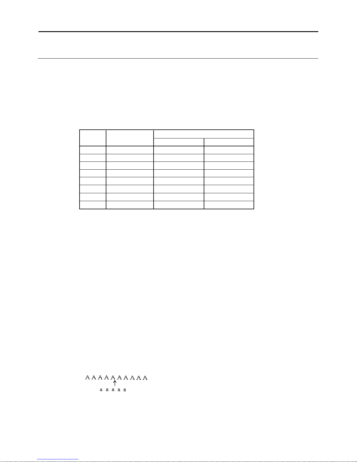
BD2-2880/2890 User’s Manual
69
ESC = n
Data Input Control
<1B>H<3D>H<n>
{0 =< n =< FF} Data is described in Hex code.
Selecting equipment in which data input from the host is effective.
• Each bit of n indicates as follows:
Va l u e Bit Equipment
0 1
0 Printer Invalid Valid
1 Not defined
2 Not defined
3 Not defined
4 Not defined
5 Not defined
6 Not defined
7 Not defined
• When the printer has not been selected, this printer abandons all the received data
until it is selected by this command.
• Even when the printer has not been selected, it can become BUSY state through
printer operation.
• When the printer is deselected, this printer discards all the data until it is selected
with this command.
• The initial value of n is "1".
LPRINT "AAAAA”;
LPRINT CHR$ (&H1B) + "=" + CHR$ (0);
LPRINT "aaaaa" + CHR$ (&HA);
LPRINT CHR$ (&H1B) + "=" + CHR$ (1);
LPRINT "AAAAA" + CHR$ (&HA);
is not printed
[Function]
[Code]
[Range]
[Outline]
[Caution]
[Default]
[Sample Program]
[Print Results]

BD2-2880/2890 User’s Manual
70
ESC @
Initializing the Printer
<1B>H<40>H
Clears data stored in the print buffer and brings various settings to the initial state (Default state).
•
Data inside the internal input buffer are not cleared.
•
Dip switches setting are red once again.
LPRINT CHR$ (&H1B) + " ! " + CHR$ (&H30) ;
LPRINT CHR$ (&H1B) + "V" + CHR$ (1);
LPRINT "AAA" + CHR$ (&HA);
LPRINT CHR$ (&H1B) + "@”;
LPRINT "AAA" + CHR$ (&HA);
[Function]
[Code]
[Range]
[Caution]
[Sample Program]
[Print Results]

BD2-2880/2890 User’s Manual
71
DC2 A n
Selecting the Print drive system
<12>H<41>H<n>
{0 =< n =< FF}
Selecting the Fixed division system or the Variable division system.
•
"n" is valid only for the lowest bit (n0).
n0 Print Drive System
0 Fixed division number system
1 Variable division number system
The initial value of n is specified by Jumper (J
5).
[Function]
[Code]
[Range]
[Outline]
[Default]

BD2-2880/2890 User’s Manual
72
12. CHARACTER CODE TABLE
12.1 International
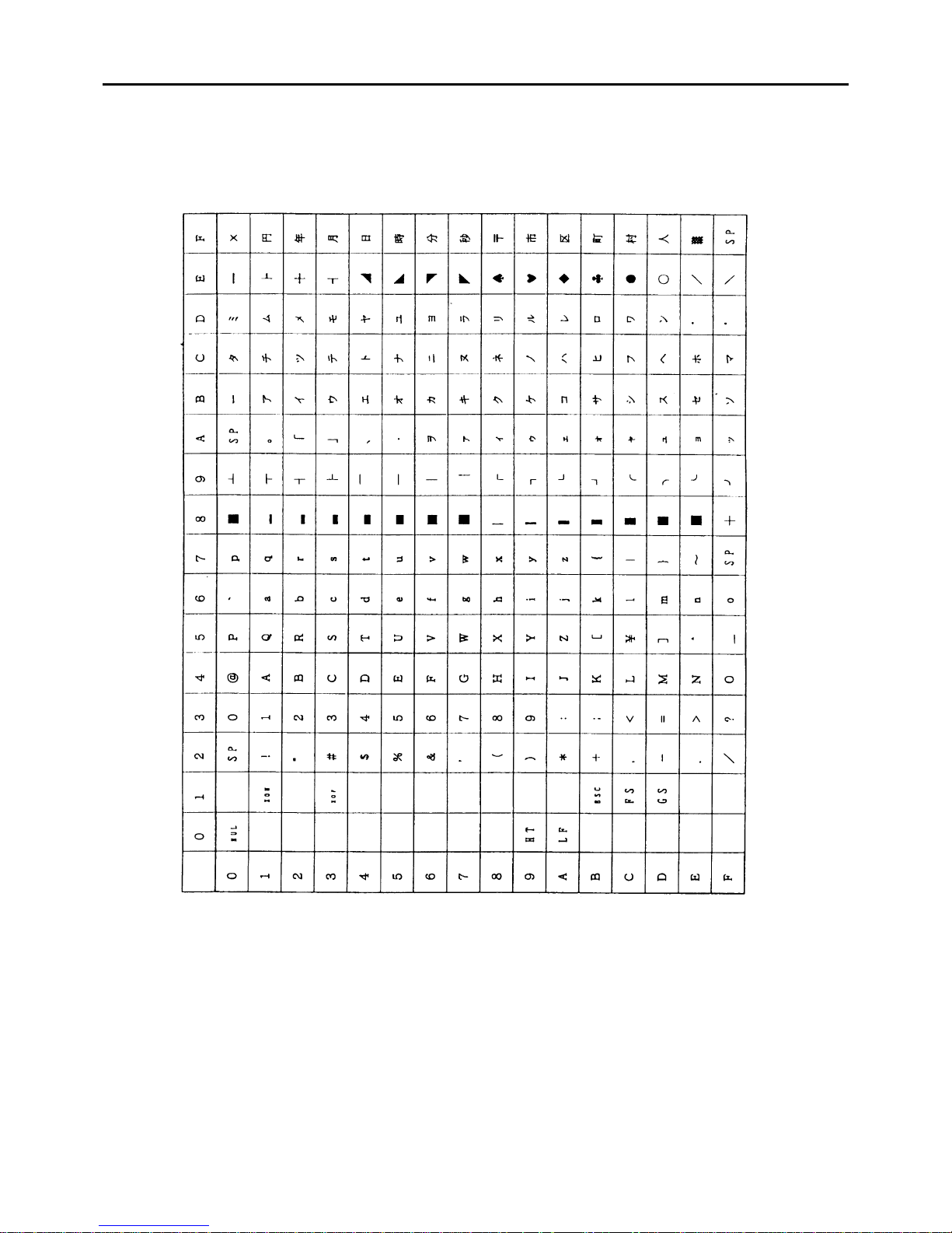
BD2-2880/2890 User’s Manual
73
12.2 Japanese
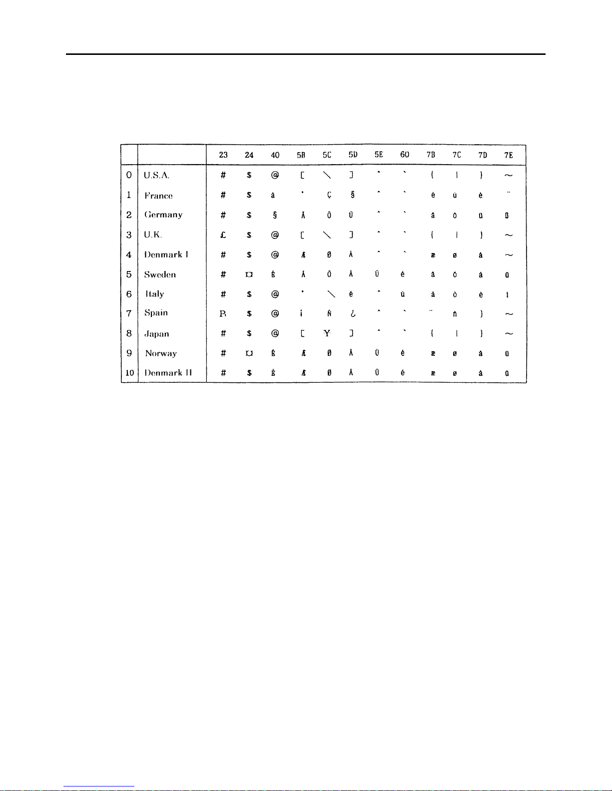
BD2-2880/2890 User’s Manual
74
12.3 International Character Set
COUNTRY
BD2-2880/2890 User’s Manual
75
APPENDIX 1. BLOCK DIAGRAM
CPU
OSC 16.0MH
FLASH
MEMORY
Driver
RAM
G/A
Reset
Cutter
Driver
Driver
Timing
Operation Panel
Stepping
Moter
Paper End
Head Up
Parallel
(Centronics)
Serial
(RS-232C)
Power Supply
CN3
Print Head

BD2-2880/2890 User’s Manual
76
APPENDIX 2. Outer Dimension
BD2–288
IC2 IC1 CN1
CN3
CN4
75
12
67
4
1.6
3
CN2
TA2
TA2
IC101
TA2
TR2
IC6
72
80
ø 2 × 4
(Unit : mm)
 Loading...