


 Loading...
CS5490
|
Two Channel Energy Measurement IC |
Features |
Description |
•Superior Analog Performance with Ultra-low Noise Level & The CS5490 is a high-accuracy, two-channel, energy measure-
|
High SNR |
|
|
|
|
|
|
|
|
|
|
|
|
|
|
|
|
ment analog front end. |
|
|
|
|
|
|
|
|
||||||||||||
• Energy Measurement Accuracy of 0.1% over a 4000:1 |
|
|
|
|
The CS5490 incorporates independent 4th order Delta-Sigma an- |
|||||||||||||||||||||||||||||||||
|
Dynamic Range |
|
|
|
|
|
|
|
|
|
|
|
|
|
|
|
|
|||||||||||||||||||||
• Two Independent 24-bit, 4th-order, Delta-Sigma |
|
|
|
|
alog-to-digital converters for both channels, reference circuitry, |
|||||||||||||||||||||||||||||||||
|
Modulators for Voltage and Current Measurements |
|
|
|
|
and the proven EXL signal processing core to provide active, re- |
||||||||||||||||||||||||||||||||
• Configurable Digital Output for Energy Pulses, Interrupt, |
|
active, and apparent energy measurement. In addition, RMS and |
||||||||||||||||||||||||||||||||||||
|
power factor calculations are available. Calculations are output |
|||||||||||||||||||||||||||||||||||||
|
zero-crossing, and Energy Direction |
|
|
|
|
|
|
|
|
|
|
|||||||||||||||||||||||||||
• Supports Shunt Resistor, CT, and Rogowski Coil Current |
|
via a configurable energy pulse, or direct UART serial access to |
||||||||||||||||||||||||||||||||||||
|
on-chip registers. Instantaneous current, voltage, and power |
|||||||||||||||||||||||||||||||||||||
|
Sensors |
|
|
|
|
|
|
|
|
|
|
|
|
|
|
|
|
|||||||||||||||||||||
• |
On-chip Measurements/Calculations: |
|
|
|
|
|
|
|
|
|
|
measurements are also |
available over |
|
the serial port. The |
|||||||||||||||||||||||
|
|
|
|
|
|
|
|
|
|
two-wire UART minimizes the cost of isolation where required. |
||||||||||||||||||||||||||||
|
- |
Active, Reactive, and Apparent Power |
|
|
|
|
|
|
|
|
|
|
||||||||||||||||||||||||||
|
|
|
|
|
|
|
|
|
|
|
|
|
|
|
|
|
|
|
|
|
|
|
|
|
|
|
|
|
||||||||||
|
- |
RMS Voltage and Current |
|
|
|
|
|
|
|
|
|
|
A configurable digital output provides energy pulses, zero-cross- |
|||||||||||||||||||||||||
|
- |
Power Factor and Line Frequency |
|
|
|
|
|
|
|
|
|
|
ing, energy direction, or interrupt functions. Interrupts can be |
|||||||||||||||||||||||||
|
- |
Instantaneous Voltage, Current, and Power |
|
|
|
|
||||||||||||||||||||||||||||||||
|
|
|
|
|
generated for a variety of conditions including voltage sag or |
|||||||||||||||||||||||||||||||||
• Overcurrent, Voltage Sag, and Voltage Swell Detection |
|
|||||||||||||||||||||||||||||||||||||
|
swell, overcurrent, and more. On-chip register integrity is assured |
|||||||||||||||||||||||||||||||||||||
• Ultra-fast On-chip Digital Calibration |
|
|
|
|
|
|
|
|
|
|
via checksum and write protection. The CS5490 is designed to in- |
|||||||||||||||||||||||||||
• Configurable No-load Threshold for Anti-creep |
|
|
|
|
terface to a variety of voltage and current sensors, including shunt |
|||||||||||||||||||||||||||||||||
• Internal Register Protection via Checksum and Write |
|
|
|
|
resistors, current transformers, and Rogowski coils. |
|||||||||||||||||||||||||||||||||
|
Protection |
|
|
|
|
|
|
|
|
|
|
|
|
|
|
|
|
On-chip functionality makes digital calibration simple and ultra |
||||||||||||||||||||
• |
UART Serial Interface |
|
|
|
|
|
|
|
|
|
|
|
|
|
|
|
|
|||||||||||||||||||||
|
|
|
|
|
|
|
|
|
|
|
|
|
|
|
|
fast to minimize the time required at the end of the customer pro- |
||||||||||||||||||||||
• On-chip Temperature Sensor |
|
|
|
|
|
|
|
|
|
|
||||||||||||||||||||||||||||
|
|
|
|
|
|
|
|
|
|
duction line. Performance across temperature is ensured with an |
||||||||||||||||||||||||||||
• On-chip Voltage Reference (25ppm/°C Typ.) |
|
|
|
|
||||||||||||||||||||||||||||||||||
|
|
|
|
on-chip voltage reference with low drift. A single 3.3V power sup- |
||||||||||||||||||||||||||||||||||
• Single 3.3 V Power Supply |
|
|
|
|
|
|
|
|
|
|
||||||||||||||||||||||||||||
|
|
|
|
|
|
|
|
|
|
ply is required, and power consumption is low at <13mW. To |
||||||||||||||||||||||||||||
• |
Ultra-fine Phase Compensation |
|
|
|
|
|
|
|
|
|
|
|||||||||||||||||||||||||||
|
|
|
|
|
|
|
|
|
|
minimize space requirements, the CS5490 is offered in a low-cost |
||||||||||||||||||||||||||||
• Low Power Consumption: <13 mW |
|
|
|
|
|
|
|
|
|
|
16-pin SOIC package. |
|
|
|
|
|
|
|
|
|||||||||||||||||||
• |
Power Supply Configurations: |
|
|
|
|
|
|
|
|
|
|
ORDERING INFORMATION |
|
|
|
|||||||||||||||||||||||
|
- GNDA = 0 V, VDDA: +3.3 V |
|
|
|
|
|
|
|
|
|
|
|
|
|
||||||||||||||||||||||||
• Low-cost 16-pin SOIC Package |
|
|
|
|
|
|
|
|
|
|
|
|
See Page 57. |
|
|
|
|
|
|
|
|
|||||||||||||||||
|
|
|
|
|
|
|
|
|
|
|
|
|
|
|
|
|
|
|
|
|
|
|
|
|
|
|
|
|||||||||||
|
|
|
|
|
|
|
|
|
|
|
|
|
|
|
|
|
|
|
|
|
|
|
|
|
|
|
|
|
|
|
|
|
||||||
|
|
|
|
|
|
VDDA |
|
|
|
|
|
|
|
|
|
|
|
|
|
|
|
|
|
|
|
|
|
|
|
VDDD |
|
|
|
|||||
|
|
|
|
|
|
|
|
|
|
|
RESET |
|
|
|
|
|
|
|||||||||||||||||||||
|
|
|
|
|
|
|
|
|
|
|
|
|
|
|
|
|
|
|
|
|
|
|
|
|
|
|
|
|
|
|
|
CS5490 |
|
|
|
|||
|
|
IIN+ |
|
|
|
|
|
|
|
|
|
|
|
|
|
|
|
|
|
|
|
|
|
|
|
|
|
|
|
|
|
|
|
|
|
|
|
|
|
|
|
|
|
|
|
|
|
4th Order |
|
|
|
|
|
Digital |
|
|
|
|
|
|
|
|
|
|
|
|
|
|
|
|
|
|
|
||||
|
|
|
|
PGA |
|
|
|
|
|
|
|
|
|
|
|
|
|
HPF |
|
|
|
|
|
|
|
|
|
|
|
|
|
|||||||
|
|
IIN- |
|
|
|
|
|
|
|
Modulator |
|
|
|
|
|
Filter |
|
|
|
|
Option |
|
|
|
|
|
|
|
|
|
|
|
|
|
||||
|
|
|
|
|
|
|
|
|
|
|
|
|
|
|
|
|
|
|
|
|
|
|
|
|
|
|
|
|
|
|
||||||||
|
|
|
|
|
|
|
|
|
|
|
|
|
|
|
|
|
|
|
|
|
|
|
|
|
|
|
|
|
|
|
|
|
|
|
|
|
|
|
|
|
|
|
|
|
|
|
|
|
|
|
|
|
|
|
|
|
|
|
|
|
|
|
|
|
|
|
|
|
|
|
|
|
UART |
|
|
RX |
|
|
|
|
|
|
|
|
|
|
|
|
|
|
|
|
|
|
|
|
|
|
|
|
|
|
|
|
|
|
|
|
|
|
|
Serial |
|
|
||
|
|
|
|
|
|
|
|
|
|
|
|
|
|
|
|
|
|
|
|
|
|
|
|
|
|
|
|
|
|
|
|
|
|
|
|
TX |
||
|
|
|
|
|
|
|
|
|
|
|
|
|
|
|
|
|
|
|
|
|
|
|
|
|
|
|
|
|
|
|
|
|
|
Interface |
|
|
||
|
|
|
|
|
|
|
|
|
|
|
|
|
|
|
|
|
|
|
|
|
|
|
|
|
|
|
|
|
|
|||||||||
|
|
VIN+ |
|
|
10x |
|
|
|
|
4th Order |
|
|
|
Digital |
|
|
|
|
HPF |
|
|
|
Calculation |
|
|
|
|
|
|
|
|
|||||||
|
|
VIN- |
|
|
|
|
|
|
Modulator |
|
|
|
|
|
Filter |
|
|
|
|
Option |
|
|
|
|
|
|
|
|
|
|
|
|||||||
|
|
|
|
|
|
|
|
|
|
|
|
|
|
|
|
|
|
|
|
|
|
|
|
|
|
|
|
|
|
|||||||||
|
|
|
|
|
|
|
|
|
|
|
|
|
|
|
|
|
|
|
|
|
|
|
|
|
|
|
|
|
|
|
|
|
|
|
|
|
|
|
|
|
|
|
|
|
|
|
|
|
|
|
|
|
|
|
|
|
|
|
|
|
|
|
|
|
|
|
|
|
|
|
|
|
Configurable |
|
|
|
|
|
|
VREF+ |
|
|
Voltage |
|
|
|
|
Temperature |
|
|
|
|
|
|
|
|
|
|
|
|
|
|
|
|
|
|
|
|
|
|
Digital |
|
|
DO |
||
|
|
|
|
|
|
|
|
|
|
|
|
|
|
|
|
|
|
|
|
|
|
|
|
|
|
|
|
|
|
|
|
|||||||
|
|
|
|
|
Reference |
|
|
|
|
Sensor |
|
|
|
|
|
|
|
|
|
|
|
|
|
|
|
|
|
|
|
|
|
|
Output |
|
|
|
|
|
|
|
|
|
|
|
|
|
|
|
|
|
|
|
|
|
|
|
|
|
|
|
|
|
|
|
|
||||||||||||
|
|
VREF- |
|
|
|
|
|
|
|
|
|
|
|
|
|
|
|
|
|
|
|
|
|
|
|
|
|
|
|
|
|
|
|
|
|
|
||
|
|
|
|
|
|
|
|
|
|
|
|
|
|
|
|
|
|
|
|
|
|
|
|
|
|
|
|
|
|
|
|
|
|
|
|
|
|
|
|
|
|
|
|
|
|
|
|
|
|
|
|
|
|
|
|
|
|
|
|
|
|
|
|
|
|
|
|
|
|
|
|
|
|
|
|||
|
|
|
|
|
|
|
|
|
|
|
System |
|
|
|
|
Clock |
|
|
|
|
|
|
|
|
|
|
|
|
|
|||||||||
|
|
|
|
|
|
|
|
|
|
|
Clock |
|
|
|
|
|
Generator |
|
|
|
|
|
|
|
|
|
|
|
|
|
||||||||
|
|
|
|
|
|
|
|
|
|
|
|
|
|
|
|
|
|
|
|
|
|
|
|
|
|
|
|
|
|
|
|
|
|
|
|
|
||
|
|
|
|
|
|
|
|
|
|
|
|
|
|
|
|
|
|
|
|
|
|
|
|
|
|
|
|
|
|
|
|
|
|
|
|
|
||
|
|
|
|
|
|
GNDA |
|
|
|
|
|
|
XIN |
|
XOUT |
|
|
|
|
|
|
MODE |
|
|
|
|||||||||||||
|
|
|
|
|
|
|
|
|
|
|
|
|
|
|
|
|
|
|
|
|
|
|
|
|
|
|
|
|
|
|
|
|
|
|
||||
Cirrus Logic, Inc. |
|
|
|
|
|
|
Copyright Cirrus Logic, Inc. 2013 |
|
|
|
|
|
|
|
|
|
MAR’13 |
|||||||||||||||||||||
http://www.cirrus.com |
|
|
|
|
|
|
|
(All Rights Reserved) |
|
|
|
|
|
|
|
|
|
DS982F3 |
||||||||||||||||||||
|
|
|
|
|
|
|
|
|
|
|
|
|
|
|
|
|
|
|
|
|
||||||||||||||||||

CS5490
TABLE OF CONTENTS
1. Overview . . . . . . . . . . . . . . . . . . . . . . . . . . . . . . . . . . . . . . . . . . . . . . . . . . . . . . . . . . . . . . . .5
2. Pin Description . . . . . . . . . . . . . . . . . . . . . . . . . . . . . . . . . . . . . . . . . . . . . . . . . . . . . . . . .6
2.1 Analog Pins . . . . . . . . . . . . . . . . . . . . . . . . . . . . . . . . . . . . . . . . . . . . . . . . . . . . . . . .6
2.1.1 Voltage Input . . . . . . . . . . . . . . . . . . . . . . . . . . . . . . . . . . . . . . . . . . . . . . . . . .6
2.1.2 Current Input . . . . . . . . . . . . . . . . . . . . . . . . . . . . . . . . . . . . . . . . . . . . . . . . . .6
2.1.3 Voltage Reference . . . . . . . . . . . . . . . . . . . . . . . . . . . . . . . . . . . . . . . . . . . . .7
2.1.4 Crystal Oscillator . . . . . . . . . . . . . . . . . . . . . . . . . . . . . . . . . . . . . . . . . . . . . . .7
2.2 Digital Pins . . . . . . . . . . . . . . . . . . . . . . . . . . . . . . . . . . . . . . . . . . . . . . . . . . . . . . . . .7
2.2.1 Reset Input . . . . . . . . . . . . . . . . . . . . . . . . . . . . . . . . . . . . . . . . . . . . . . . . . . .7
2.2.2 Digital Output . . . . . . . . . . . . . . . . . . . . . . . . . . . . . . . . . . . . . . . . . . . . . . . . .7
2.2.3 UART Serial Interface . . . . . . . . . . . . . . . . . . . . . . . . . . . . . . . . . . . . . . . . . . .7
2.2.3.1 UART . . . . . . . . . . . . . . . . . . . . . . . . . . . . . . . . . . . . . . . . . . . . . . . . . .7
2.2.4 MODE Pin . . . . . . . . . . . . . . . . . . . . . . . . . . . . . . . . . . . . . . . . . . . . . . . . . . . .7
3. Characteristics & Specifications . . . . . . . . . . . . . . . . . . . . . . . . . . . . . . . . . . . . . . . . . . . . |
.8 |
|
4. Signal Flow Description . . . . . . . . . . . . . . . . . . . . . . . . . . . . . . . . . . . . . . . . . . . . . . . . . . . |
15 |
|
4.1 |
Analog-to-Digital Converters . . . . . . . . . . . . . . . . . . . . . . . . . . . . . . . . . . . . . . . . . . |
15 |
4.2 |
Decimation Filters . . . . . . . . . . . . . . . . . . . . . . . . . . . . . . . . . . . . . . . . . . . . . . . . . . |
15 |
4.3 |
IIR Filter . . . . . . . . . . . . . . . . . . . . . . . . . . . . . . . . . . . . . . . . . . . . . . . . . . . . . . . . . . |
15 |
4.4 |
Phase Compensation . . . . . . . . . . . . . . . . . . . . . . . . . . . . . . . . . . . . . . . . . . . . . . . |
15 |
4.5 |
DC Offset & Gain Correction . . . . . . . . . . . . . . . . . . . . . . . . . . . . . . . . . . . . . . . . . . |
15 |
4.6 |
High-pass & Phase Matching Filters . . . . . . . . . . . . . . . . . . . . . . . . . . . . . . . . . . . . |
16 |
4.7 |
Digital Integrators . . . . . . . . . . . . . . . . . . . . . . . . . . . . . . . . . . . . . . . . . . . . . . . . . . . |
16 |
4.8 |
Low-rate Calculations . . . . . . . . . . . . . . . . . . . . . . . . . . . . . . . . . . . . . . . . . . . . . . . |
16 |
|
4.8.1 Fixed Number of Samples Averaging . . . . . . . . . . . . . . . . . . . . . . . . . . . . . . |
16 |
|
4.8.2 Line-cycle Synchronized Averaging . . . . . . . . . . . . . . . . . . . . . . . . . . . . . . . |
16 |
|
4.8.3 RMS Current & Voltage . . . . . . . . . . . . . . . . . . . . . . . . . . . . . . . . . . . . . . . . |
17 |
|
4.8.4 Active Power . . . . . . . . . . . . . . . . . . . . . . . . . . . . . . . . . . . . . . . . . . . . . . . . . |
17 |
|
4.8.5 Reactive Power . . . . . . . . . . . . . . . . . . . . . . . . . . . . . . . . . . . . . . . . . . . . . . . |
17 |
|
4.8.6 Apparent Power . . . . . . . . . . . . . . . . . . . . . . . . . . . . . . . . . . . . . . . . . . . . . . |
17 |
|
4.8.7 Peak Voltage & Current . . . . . . . . . . . . . . . . . . . . . . . . . . . . . . . . . . . . . . . . |
17 |
|
4.8.8 Power Factor . . . . . . . . . . . . . . . . . . . . . . . . . . . . . . . . . . . . . . . . . . . . . . . . . |
17 |
4.9 |
Average Active Power Offset . . . . . . . . . . . . . . . . . . . . . . . . . . . . . . . . . . . . . . . . . . |
17 |
4.10 Average Reactive Power Offset . . . . . . . . . . . . . . . . . . . . . . . . . . . . . . . . . . . . . . . |
17 |
|
5. Functional Description . . . . . . . . . . . . . . . . . . . . . . . . . . . . . . . . . . . . . . . . . . . . . . . . . . . .18
5.1 Power-on Reset (POR) . . . . . . . . . . . . . . . . . . . . . . . . . . . . . . . . . . . . . . . . . . . . . .18
5.2 Power Saving Modes . . . . . . . . . . . . . . . . . . . . . . . . . . . . . . . . . . . . . . . . . . . . . . . .18
5.3 Zero-crossing Detection . . . . . . . . . . . . . . . . . . . . . . . . . . . . . . . . . . . . . . . . . . . . . .18
5.4 Line Frequency Measurement . . . . . . . . . . . . . . . . . . . . . . . . . . . . . . . . . . . . . . . . .19
5.5 Energy Pulse Generation . . . . . . . . . . . . . . . . . . . . . . . . . . . . . . . . . . . . . . . . . . . . .19
5.5.1 Pulse Rate . . . . . . . . . . . . . . . . . . . . . . . . . . . . . . . . . . . . . . . . . . . . . . . . . .20
5.5.2 Pulse Width . . . . . . . . . . . . . . . . . . . . . . . . . . . . . . . . . . . . . . . . . . . . . . . . . .21
5.6 Voltage Sag, Voltage Swell, and Overcurrent Detection . . . . . . . . . . . . . . . . . . . . .21
5.7 Phase Sequence Detection . . . . . . . . . . . . . . . . . . . . . . . . . . . . . . . . . . . . . . . . . . .22
5.8 Temperature Measurement . . . . . . . . . . . . . . . . . . . . . . . . . . . . . . . . . . . . . . . . . . .23
2 |
DS982F3 |

CS5490
5.9 Anti-creep . . . . . . . . . . . . . . . . . . . . . . . . . . . . . . . . . . . . . . . . . . . . . . . . . . . . . . . . 23
5.10 Register Protection . . . . . . . . . . . . . . . . . . . . . . . . . . . . . . . . . . . . . . . . . . . . . . . . 23
5.10.1 Write Protection . . . . . . . . . . . . . . . . . . . . . . . . . . . . . . . . . . . . . . . . . . . . . 23
5.10.2 Register Checksum . . . . . . . . . . . . . . . . . . . . . . . . . . . . . . . . . . . . . . . . . . 23
6. Host Commands and Registers . . . . . . . . . . . . . . . . . . . . . . . . . . . . . . . . . . . . . . . . . . . . 24
6.1 Host Commands . . . . . . . . . . . . . . . . . . . . . . . . . . . . . . . . . . . . . . . . . . . . . . . . . . . 24
6.1.1 Memory Access Commands . . . . . . . . . . . . . . . . . . . . . . . . . . . . . . . . . . . . . 24
6.1.1.1 Page Select . . . . . . . . . . . . . . . . . . . . . . . . . . . . . . . . . . . . . . . . . . . . 24
6.1.1.2 Register Read . . . . . . . . . . . . . . . . . . . . . . . . . . . . . . . . . . . . . . . . . . 24
6.1.1.3 Register Write . . . . . . . . . . . . . . . . . . . . . . . . . . . . . . . . . . . . . . . . . . 24
6.1.2 Instructions . . . . . . . . . . . . . . . . . . . . . . . . . . . . . . . . . . . . . . . . . . . . . . . . . . 24
6.1.3 Checksum . . . . . . . . . . . . . . . . . . . . . . . . . . . . . . . . . . . . . . . . . . . . . . . . . . . 25
6.1.4 Serial Time Out . . . . . . . . . . . . . . . . . . . . . . . . . . . . . . . . . . . . . . . . . . . . . . . 25
6.2 Hardware Registers Summary (Page 0) . . . . . . . . . . . . . . . . . . . . . . . . . . . . . . . . . 26
6.3 Software Registers Summary (Page 16) . . . . . . . . . . . . . . . . . . . . . . . . . . . . . . . . . 28
6.4 Software Registers Summary (Page 17) . . . . . . . . . . . . . . . . . . . . . . . . . . . . . . . . . 30
6.5 Software Registers Summary (Page 18) . . . . . . . . . . . . . . . . . . . . . . . . . . . . . . . . . 31
6.6 Register Descriptions . . . . . . . . . . . . . . . . . . . . . . . . . . . . . . . . . . . . . . . . . . . . . . . 32
7. System Calibration . . . . . . . . . . . . . . . . . . . . . . . . . . . . . . . . . . . . . . . . . . . . . . . . . . . . . . . 52
7.1 Calibration in General . . . . . . . . . . . . . . . . . . . . . . . . . . . . . . . . . . . . . . . . . . . . . . . 52
7.1.1 Offset Calibration . . . . . . . . . . . . . . . . . . . . . . . . . . . . . . . . . . . . . . . . . . . . . 52
7.1.1.1 DC Offset Calibration . . . . . . . . . . . . . . . . . . . . . . . . . . . . . . . . . . . . 52
7.1.1.2 AC Offset Calibration . . . . . . . . . . . . . . . . . . . . . . . . . . . . . . . . . . . . . 52
7.1.2 Gain Calibration . . . . . . . . . . . . . . . . . . . . . . . . . . . . . . . . . . . . . . . . . . . . . . 53
7.1.3 Calibration Order . . . . . . . . . . . . . . . . . . . . . . . . . . . . . . . . . . . . . . . . . . . . . 53
7.2 Phase Compensation . . . . . . . . . . . . . . . . . . . . . . . . . . . . . . . . . . . . . . . . . . . . . . . 53
7.3 Temperature Sensor Calibration . . . . . . . . . . . . . . . . . . . . . . . . . . . . . . . . . . . . . . . 54
7.3.1 Temperature Offset and Gain Calibration . . . . . . . . . . . . . . . . . . . . . . . . . . . 54
8. Basic Application Circuits . . . . . . . . . . . . . . . . . . . . . . . . . . . . . . . . . . . . . . . . . . . . . . . . . 55
9. Package Dimensions . . . . . . . . . . . . . . . . . . . . . . . . . . . . . . . . . . . . . . . . . . . . . . . . . . . . . 56
10. Ordering Information . . . . . . . . . . . . . . . . . . . . . . . . . . . . . . . . . . . . . . . . . . . . . . . . . . . 57
11. Environmental, Manufacturing, & Handling Information . . . . . . . . . . . . . . . . . . . . . . . 57
12. Revision History . . . . . . . . . . . . . . . . . . . . . . . . . . . . . . . . . . . . . . . . . . . . . . . . . . . . . . . . 57
DS982F3 |
3 |

|
CS5490 |
|
LIST OF FIGURES |
Figure 1. Oscillator Connections................................................................................................... |
7 |
Figure 2. UART Serial Frame Format........................................................................................... |
7 |
Figure 3. Active Energy Load Performance.................................................................................. |
8 |
Figure 4. Reactive Energy Load Performance.............................................................................. |
9 |
Figure 5. IRMS Load Performance ............................................................................................... |
9 |
Figure 6. Signal Flow for V, I, P, and Q Measurements ............................................................. |
15 |
Figure 7. Low-rate Calculations .................................................................................................. |
16 |
Figure 8. Power-on Reset Timing ............................................................................................... |
18 |
Figure 9. Zero-crossing Level and Zero-crossing Output on DO................................................ |
19 |
Figure 10. Energy Pulse Generation and Digital Output Control ................................................ |
20 |
Figure 11. Sag, Swell, & Overcurrent Detect.............................................................................. |
21 |
Figure 12. Phase Sequence A, B, C for Rising Edge Transition ................................................ |
22 |
Figure 13. Phase Sequence C, B, A for Rising Edge Transition ................................................ |
23 |
Figure 14. Byte Sequence for Page Select................................................................................. |
24 |
Figure 15. Byte Sequence for Register Read ............................................................................ |
24 |
Figure 16. Byte Sequence for Register Write ............................................................................. |
24 |
Figure 17. Byte Sequence for Instructions.................................................................................. |
24 |
Figure 18. Byte Sequence for Checksum ................................................................................... |
25 |
Figure 19. Calibration Data Flow ................................................................................................ |
52 |
Figure 20. T Register vs. Force Temp ........................................................................................ |
54 |
Figure 21. Typical Connection Diagram (Single-phase, Two-wire, Power Meter) ...................... |
55 |
LIST OF TABLES
Table 1. POR Thresholds . . . . . . . . . . . . . . . . . . . . . . . . . . . . . . . . . . . . . . . . . . . . . . . . . . . . . 18
Table 2. Command Format . . . . . . . . . . . . . . . . . . . . . . . . . . . . . . . . . . . . . . . . . . . . . . . . . . . . 24
Table 3. Instruction Format . . . . . . . . . . . . . . . . . . . . . . . . . . . . . . . . . . . . . . . . . . . . . . . . . . . . 24
4 |
DS982F3 |

CS5490
1. OVERVIEW
The CS5490 is a CMOS power measurement integrated circuit that uses two analog-to-digital converters to measure line voltage and current. The CS5490 calculates active, reactive, and apparent power as well as RMS voltage and current and peak voltage and current. It handles other system-related functions, such as energy pulse generation, voltage sag and swell, overcurrent and zero-crossing detection, and line frequency measurement. A separate analog-to-digital converter is used for on-chip temperature measurement.
The CS5490 is optimized to interface to current transformers, shunt resistors, or Rogowski coils for current measurement, and to resistive dividers or voltage transformers for voltage measurement. Two full-scale ranges are provided on the current input to accommodate different types of current sensors. The CS5490’s two differential inputs have a common-mode input range from analog ground (GNDA) to the positive analog supply (VDDA).
An on-chip voltage reference (typically 2.4 volts) is generated and provided at analog output, VREF±.
The digital output (DO) provides a variety of output signals and, depending on the mode selected, provides energy pulses, zero-crossings, or other choices.
The CS5490 includes a UART serial host interface to an external microcontroller. The UART signals include serial data input (RX) and serial data output (TX).
DS982F3 |
5 |

CS5490
2. PIN DESCRIPTION
|
XOUT |
|
1 |
16 |
|
VDDD |
|
|
|
||||||
|
|
||||||
|
XIN |
|
2 |
15 |
|
MODE |
|
|
|
||||||
|
|
||||||
|
|
|
|
3 |
14 |
|
RX |
RESET |
|
|
|||||
|
|
||||||
|
IIN- |
|
4 |
13 |
|
TX |
|
|
|
||||||
|
IIN+ |
|
5 |
12 |
|
DO |
|
|
|
||||||
|
VIN+ |
|
6 |
11 |
|
VDDA |
|
|
|
||||||
|
|
||||||
|
VIN- |
|
7 |
10 |
|
GNDA |
|
|
|
||||||
|
|
||||||
|
VREF- |
|
8 |
9 |
|
VREF+ |
|
|
|
||||||
|
|
||||||
|
|
|
|
|
|
|
|
Clock Generator
Crystal In |
2,1 |
XIN, XOUT — Connect to an external quartz crystal. Alternatively, an external clock can be |
|
Crystal Out |
|
supplied to the XIN pin to provide the system clock for the device. |
|
Control Pins and Serial Data I/O |
|
|
|
Digital Output |
12 |
DO — Configurable digital output for energy pulses, interrupt, energy direction, and |
|
|
|
zero-crossings. |
|
Reset |
3 |
|
— An active-low Schmitt-trigger input used to reset the chip. |
RESET |
|||
Serial Interface |
13,14 |
TX, RX — UART serial data output/input. |
|
Operating Mode Select |
15 |
MODE — Connect to VDDA for proper operation. |
|
Analog Inputs/Outputs |
|
|
|
|
|
|
|
Voltage Input |
6,7 |
VIN+, VIN- — Differential analog input for the voltage channel. |
|
|
|
|
|
Current Input |
5,4 |
IIN+, IIN- — Differential analog input for the current channel. |
|
|
|
|
|
Voltage Reference Input |
9,8 |
VREF+, VREF- — The voltage reference output and return. |
|
Power Supply Connections |
|
|
|
Internal Digital Supply |
16 |
VDDD — Decoupling pin for the internal digital supply. |
|
|
|
|
|
Positive Analog Supply |
11 |
VDDA — The positive analog supply. |
|
Analog Ground |
10 |
GNDA — Analog ground. |
|
|
|
|
|
2.1 Analog Pins |
|
|
|
|
|
|
2.1.2 Current Input |
|||
The CS5490 has two differential inputs, one for voltage |
The output of the current-sensing shunt resistor or |
|||||||||
|
|
|
|
IIN |
|
|
|
|
transformer is connected to the IIN input pins of the |
|
(VIN ) and one for current |
|
). The CS5490 also has |
CS5490. To accommodate different current-sensing |
|||||||
|
|
|
|
|
|
|
|
|
||
two voltage reference pins (VREF ) between which a |
elements, the current channel incorporates a |
|||||||||
0.1µ bypass capacitor must be placed. |
|
|
||||||||
2.1.1 Voltage Input |
|
|
|
|
|
|
programmable gain amplifier (PGA) with two selectable |
|||
|
|
|
|
|
|
input gains, as described in the Config0 register |
||||
The output |
of |
the line |
voltage |
resistive |
divider |
or |
description 6.6.1 Configuration 0 (Config0) – Page 0, |
|||
transformer |
is |
connected to |
the |
|
|
the |
Address 0 on page 32. There is a 10x gain setting and |
|||
VIN input of |
a 50x gain setting. The full-scale signal level for the |
|||||||||
CS5490. The voltage channel is equipped with a 10x, |
||||||||||
fixed-gain amplifier. The full-scale signal level that can |
current channel is ±50mV and ±250mV for 50x and 10x |
|||||||||
be applied to the voltage channel is ±250 mV. If the |
gain settings, respectively. If the input signal is a sine |
|||||||||
wave, the maximum RMS voltage is 35.35 mVRMS or |
||||||||||
input signal |
is |
a sine |
wave, the maximum RMS |
|||||||
voltage is 250mVp / 2 176.78mVRMS, |
which |
is |
176.78mVRMS, which is approximately 70.7% of |
|||||||
maximum peak voltage. |
||||||||||
approximately 70.7% of maximum peak voltage. |
|
|
||||||||
6 |
|
|
|
|
|
|
|
|
DS982F3 |
|
2.1.3 Voltage Reference
The CS5490 generates a stable voltage reference of 2.4V between the VREF pins. The reference system also requires a filter capacitor of at least 0.1µF between the VREF pins.
The reference system is capable of providing a reference for the CS5490 but has limited ability to drive external circuitry. It is strongly recommended that nothing other than the required filter capacitor is connected to the VREF pins.
2.1.4 Crystal Oscillator
An external, 4.096MHz quartz crystal can be connected to the XIN and XOUT pins as shown in Figure 1. To reduce system cost, each pin is supplied with an on-chip load capacitor.
|
|
|
|
|
|
|
|
|
|
|
|
|
|
|
|
|
|
|
|
|
|
|
|
|
|
|
|
|
|
|
|
|
|
|
|
|
|
|
|
|
|
|
|
|
|
XIN |
XOUT |
|||||||
|
|
|
|
|
|
|
|
|
|
|
|
|
|
|
|
|
|
|
|
|
|
|
|
|
|
|
|
|
|
|
|
|
|
|
|
|
|
|
|
|
|
|
|
|
|
|
|
|
|
|
C1 = 22pF |
|
C2 = 22pF |
||
Figure 1. Oscillator Connections
Alternatively, an external clock source can be connected to the XIN pin.
2.2 Digital Pins
2.2.1 Reset Input
The active-low RESET pin, when asserted for longer than 120µs, will halt all CS5490 operations and reset internal hardware registers and states. When de-asserted, an initialization sequence begins, setting the default register values. To prevent erroneous, noise-induced resets to the part, an external pull-up resistor and a decoupling capacitor are necessary on the RESET pin.
CS5490
2.2.2 Digital Output
The CS5490 provides a configurable digital output (DO). It can be configured to output energy pulses, interrupt, zero-crossings, or energy directions. Refer to the description of the Config1 register in section 6.6 Register Descriptions on page 32 for more details.
2.2.3 UART Serial Interface
The CS5490 provides two pins, RX and TX, for communication between a host microcontroller and the CS5490.
2.2.3.1 UART
The CS5490 provides a two-wire, asynchronous, full-duplex UART port. The CS5490 UART operates in 8-bit mode, which transmits a total of 10 bits per byte. Data is transmitted and received LSB first, with one start bit, eight data bits, and one stop bit.
IDLE |
START |
0 |
1 |
2 |
3 |
4 |
5 |
6 |
7 |
STOP |
IDLE |
|
|
|
|
|
|
|
|
|
|
|
|
DATA
Figure 2. UART Serial Frame Format
The baud rate is defined in the SerialCtrl register. After chip reset, the default baud rate is 600, if MCLK is 4.096MHz. The baud rate is based on the contents of bits BR[15:0] in the SerialCtrl register and is calculated as follows:
BR[15:0] = Baud Rate x (524288/MCLK) or
Baud Rate = BR[15:0] / (524288/MCLK)
The maximum baud rate is 512K if MCLK is 4.096MHz.
The UART has two signals: TX and RX. TX is the serial data output from the CS5490; RX is the serial data input to the CS5490.
2.2.4 MODE Pin
The MODE pin must be tied to VDDA for normal operation. The MODE pin is used primarily for factory test procedures.
DS982F3 |
7 |
CS5490
3. CHARACTERISTICS & SPECIFICATIONS
RECOMMENDED OPERATING CONDITIONS
Parameter |
Symbol |
Min |
Typ |
Max |
Unit |
Positive Analog Power Supply |
VDDA |
3.0 |
3.3 |
3.6 |
V |
Specified Temperature Range |
TA |
-40 |
- |
+85 |
°C |
POWER MEASUREMENT CHARACTERISTICS
|
Parameter |
Symbol |
Min |
Typ |
Max |
Unit |
|
Active Energy |
All Gain Ranges |
PAvg |
- |
±0.1 |
- |
% |
|
(Note 1 & 2) |
Current Channel Input Signal Dynamic Range 4000:1 |
||||||
|
|
|
|
|
|||
Reactive Energy |
All Gain Ranges |
QAvg |
- |
±0.1 |
- |
% |
|
(Note 1 & 2) |
Current Channel Input Signal Dynamic Range 4000:1 |
||||||
|
|
|
|
|
|||
Apparent Power |
All Gain Ranges |
S |
- |
±0.1 |
- |
% |
|
(Note 1 & 3) |
Current Channel Input Signal Dynamic Range 1000:1 |
||||||
|
|
|
|
|
|||
Current RMS |
All Gain Ranges |
IRMS |
- |
±0.1 |
- |
% |
|
(Note 1, 3, & 4) |
Current Channel Input Signal Dynamic Range 1000:1 |
||||||
|
|
|
|
|
|||
Voltage RMS |
|
VRMS |
- |
±0.1 |
- |
% |
|
(Note 1 & 3) |
Voltage Channel Input Signal Dynamic Range 20:1 |
||||||
|
|
|
|
|
|||
Power Factor |
All Gain Ranges |
PF |
- |
±0.1 |
- |
% |
|
(Note 1 & 3) |
Current Channel Input Signal Dynamic Range 1000:1 |
||||||
|
|
|
|
|
Notes: 1. Specifications guaranteed by design and characterization.
2.Active energy is tested with power factor PF = 1.0. Reactive energy is tested with Sin( ) = 1.0. Energy error measured at system level using single energy pulse. Where: 1) One energy pulse = 0.5Wh or 0.5Varh; 2) VDDA = +3.3V, TA = 25°C, MCLK = 4.096MHz; 3) System is calibrated.
3.Calculated using register values; N≥4000.
4.IRMS error calculated using register values. 1) VDDA = +3.3V; TA = 25°C; MCLK = 4.096MHz; 2) AC offset calibration applied.
TYPICAL LOAD PERFORMANCE
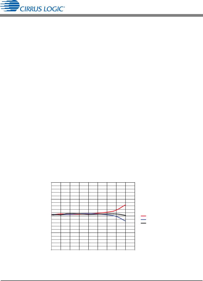
•Energy error measured at system level using single energy pulse; where 1 energy pulse = 0.5Wh or 0.5Varh.
•IRMS error calculated using register values
•VDDA = +3.3V; TA = 25°C; MCLK = 4.096MHz
Percent Error (%)
1
0.5
0
Lagging PF = 0.5
Leading PF = 0.5
PF = 1
-0.5
-1
0 |
500 |
1000 |
1500 |
2000 |
2500 |
3000 |
3500 |
4000 |
4500 |
Current Dynamic Range (x : 1)
Figure 3. Active Energy Load Performance
8 |
DS982F3 |

CS5490
Percent Error (%)
1
0.5
0 |
Lagging sin( ) = 0.5 |
Leading sin( ) = 0.5
sin( ) = 1
-0.5
-1
0 |
500 |
1000 |
1500 |
2000 |
2500 |
3000 |
3500 |
4000 |
4500 |
Current Dynamic Range (x : 1)
Figure 4. Reactive Energy Load Performance
Percent Error (%)
1
0.5
0
-0.5
-1
0 |
500 |
1000 |
1500 |
Current Dynamic range (x : 1)
IRMSErrror
RMS
Figure 5. IRMS Load Performance
DS982F3 |
9 |

CS5490
ANALOG CHARACTERISTICS
•Min/Max characteristics and specifications are guaranteed over all Recommended Operating Conditions.
•Typical characteristics and specifications are measured at nominal supply voltages and TA = 25°C.
•VDDA = +3.3V ±10%; GNDA = 0V. All voltages with respect to 0V.
•MCLK = 4.096MHz.
Parameter |
|
Symbol |
Min |
Typ |
Max |
Unit |
|
Analog Inputs (Current Channels) |
|
|
|
|
|
|
|
Common Mode Rejection |
(DC, 50, 60Hz) |
CMRR |
80 |
- |
- |
dB |
|
Common Mode+Signal |
|
|
-0.25 |
- |
VDDA |
V |
|
|
|
|
|
|
|
|
|
Differential Full-scale Input Range |
(Gain = 10) |
IIN |
- |
250 |
- |
mVP |
|
[(IIN+) – (IIN-)] |
(Gain = 50) |
- |
50 |
- |
mVP |
||
|
|
|
|
||||
|
|
|
|
|
|
|
|
Total Harmonic Distortion |
(Gain = 50) |
THD |
90 |
100 |
- |
dB |
|
Signal-to-Noise Ratio (SNR) |
(Gain = 10) |
SNR |
- |
80 |
- |
dB |
|
|
(Gain = 50) |
- |
80 |
- |
dB |
||
|
|
||||||
|
|
|
|
|
|
|
|
Crosstalk from Voltage Inputs at Full Scale |
(50, 60Hz) |
|
- |
-115 |
- |
dB |
|
Crosstalk from Current Input at Full Scale |
(50, 60Hz) |
|
- |
-115 |
- |
dB |
|
Input Capacitance |
|
IC |
- |
27 |
- |
pF |
|
Effective Input Impedance |
|
EII |
30 |
- |
- |
k |
|
Offset Drift (Without the High-pass Filter) |
|
OD |
- |
4.0 |
- |
µV/°C |
|
Noise (Referred to Input) |
(Gain = 10) |
NI |
- |
9 |
- |
µVRMS |
|
|
(Gain = 50) |
- |
2.2 |
- |
µVRMS |
||
|
|
|
|||||
Power Supply Rejection Ratio |
(60Hz) |
|
|
|
|
|
|
(Note 7) |
(Gain = 10) |
PSRR |
60 |
65 |
- |
dB |
|
|
(Gain = 50) |
|
68 |
75 |
- |
dB |
|
|
|
|
|
|
|
|
|
Analog Inputs (Voltage Channels) |
|
|
|
|
|
|
|
Common Mode Rejection |
(DC, 50, 60Hz) |
CMRR |
80 |
- |
- |
dB |
|
Common Mode+Signal |
|
|
-0.25 |
- |
VDDA |
V |
|
Differential Full-scale Input Range |
[(VIN+) – (VIN-)] |
VIN |
- |
250 |
- |
mVP |
|
Total Harmonic Distortion |
|
THD |
80 |
88 |
- |
dB |
|
Signal-to-Noise Ratio (SNR) |
|
SNR |
- |
73 |
- |
dB |
|
Crosstalk from Current Inputs at Full Scale |
(50, 60Hz) |
|
- |
-115 |
- |
dB |
|
Input Capacitance |
|
IC |
- |
2.0 |
- |
pF |
|
Effective Input Impedance |
|
EII |
2 |
- |
- |
M |
|
Noise (Referred to Input) |
|
NV |
- |
40 |
- |
µVRMS |
|
Offset Drift (Without the High-pass Filter) |
|
OD |
- |
16.0 |
- |
µV/°C |
|
|
|
|
|
|
|
|
|
Power Supply Rejection Ratio |
(60Hz) |
PSRR |
60 |
65 |
- |
dB |
|
(Note 7) |
(Gain = 10) |
||||||
|
|
|
|
|
|||
Temperature |
|
|
|
|
|
|
|
Temperature Accuracy |
(Note 6) |
T |
- |
±5 |
- |
°C |
10 |
DS982F3 |
CS5490
|
|
|
|
|
|
|
|
|
|
|
|
|
|
|
|
|
|
|
|
Parameter |
|
Symbol |
Min |
Typ |
Max |
Unit |
|
|
|
|
|
|
|
|
|
|
Power Supplies |
|
|
|
|
|
|
|
|
Power Supply Currents (Active State) |
IA+ (VDDA = +3.3V) |
PSCA |
- |
3.9 |
- |
mA |
|
|
Power Consumption |
|
|
|
|
|
|
|
|
(Note 5) |
Active State (VDDA = +3.3V) |
PC |
- |
12.9 |
- |
mW |
|
|
|
|
Stand-by State |
|
- |
4.5 |
- |
mW |
|
|
|
|
|
|
|
|
|
|
Notes: |
5. All outputs unloaded. All inputs CMOS level. |
|
|
|
|
|
|
6.Temperature accuracy measured after calibration is performed.
7.Measurement method for PSRR: VDDA = +3.3V, a 150mV (zero-to-peak) (60Hz) sinewave is imposed onto the +3.3V DC supply voltage at the VDDA pin. The “+” and “-” input pins of both input channels are shorted to GNDA. The CS5490 is then commanded to continuous conversion acquisition mode, and digital output data is collected for the channel under test. The (zero-to-peak) value of the digital sinusoidal output signal is determined, and this value is converted into the (zero-to-peak) value of the sinusoidal voltage (measured in mV) that would need to be applied at the channel’s inputs, in order to cause the same digital sinusoidal output. This voltage is then defined as Veq PSRR is (in dB):
PSRR = 20 log |
150 |
---------- |
|
|
Veq |
|
VOLTAGE REFERENCE
Parameter |
|
Symbol |
Min |
Typ |
Max |
Unit |
Reference |
(Note 8) |
|
|
|
|
|
Output Voltage |
|
VREF |
+2.3 |
+2.4 |
+2.5 |
V |
Temperature Coefficient |
(Note 9) |
TCVREF |
- |
25 |
- |
ppm/°C |
Load Regulation |
(Note 10) |
VR |
- |
30 |
- |
mV |
Notes: 8. It is strongly recommended that no connection other than the required filter capacitor be made to VREF±.
9.The voltage at VREF± is measured across the temperature range. From these measurements the following formula is used to calculate the VREF temperature coefficient:
|
|
VREFMAX – VREFMIN |
|
1 |
|
|
|
6 |
|
TCVREF = |
|
--------------------------------------------- |
1.0 |
10 |
|
||||
|
-----------------------------------------------------------VREFAVG - |
|
|
|
|||||
|
TAMAX – TAMIN |
|
|
|
|
||||
|
|
|
|
|
|
|
|
10.Specified at maximum recommended output of 1µA sourcing. VREF is a very sensitive signal, the output of the VREF circuit has a very high output impedance so that the 0.1µF reference capacitor provides attenuation even to low frequency noise, such as 50Hz noise on the VREF output. As such VREF intended for the CS5490 only and should not be connected to any external circuitry. The output impedance is sufficiently high that standard digital multi-meters can significantly load this voltage. The accuracy of the metrology IC can not be guaranteed when a multimeter or any component other than the 0.1µF capacitor is attached to VREF. If it is desired to measure VREF for any reason other than a very course indicator of VREF functionality, Cirrus recommends a very high input impedance multimeter such as the Keithley Model 2000 Digital Multimeter be used, but still cannot guarantee the accuracy of the metrology with this meter connected to VREF.
DS982F3 |
11 |

CS5490
DIGITAL CHARACTERISTICS
•Min / Max characteristics and specifications are guaranteed over all Recommended Operating Conditions.
•Typical characteristics and specifications are measured at nominal supply voltages and TA = 25°C.
•VDDA = +3.3V ±10%; GNDA = 0V. All voltages with respect to 0V.
•MCLK = 4.096MHz.
Parameter |
|
Symbol |
Min |
Typ |
Max |
Unit |
Master Clock Characteristics |
|
|
|
|
|
|
XIN Clock Frequency |
Internal Gate Oscillator |
MCLK |
2.5 |
4.096 |
5 |
MHz |
XIN Clock Duty Cycle |
|
|
40 |
- |
60 |
% |
Filter Characteristics |
|
|
|
|
|
|
Phase Compensation Range |
(60Hz, OWR = 4000Hz) |
|
-10.79 |
- |
+10.79 |
° |
Input Sampling Rate |
|
|
- |
MCLK/8 |
- |
Hz |
Digital Filter Output Word Rate |
(Both channels) |
OWR |
- |
MCLK/1024 |
- |
Hz |
High-pass Filter Corner Frequency |
-3dB |
|
- |
2.0 |
- |
Hz |
Input/Output Characteristics |
|
|
|
|
|
|
High-level Input Voltage (All Pins) |
|
VIH |
0.6(VDDA) |
- |
- |
V |
Low-level Input Voltage (All Pins) |
|
VIL |
- |
- |
0.6 |
V |
High-level Output Voltage |
DO, Iout = +10mA |
VOH |
VDDA-0.3 |
- |
- |
V |
(Note 12) |
Iout = +5mA |
VDDA-0.3 |
- |
- |
V |
|
Low-level Output Voltage |
DO, Iout = -12mA |
VOL |
- |
- |
0.5 |
V |
(Note 12) |
All Other Outputs, Iout = -5mA |
- |
- |
0.5 |
V |
|
Input Leakage Current |
|
Iin |
- |
±1 |
±10 |
µA |
3-state Leakage Current |
|
IOZ |
- |
- |
±10 |
µA |
Digital Output Pin Capacitance |
|
Cout |
- |
5 |
- |
pF |
Notes: 11. All measurements performed under static conditions.
12.XOUT pin used for crystal only. Typical drive current<1mA.
12 |
DS982F3 |

CS5490
SWITCHING CHARACTERISTICS
•Min / Max characteristics and specifications are guaranteed over all Recommended Operating Conditions.
•Typical characteristics and specifications are measured at nominal supply voltages and TA = 25°C.
•VDDA = +3.3V ±10%; GNDA = 0V. All voltages with respect to 0V.
•Logic Levels: Logic 0 = 0V, Logic 1 = VDDA.
Parameter |
|
Symbol |
Min |
Typ |
Max |
Unit |
Rise Times |
DO |
trise |
- |
- |
1.0 |
µs |
(Note 13) |
Any Digital Output Except DO |
- |
50 |
- |
ns |
|
Fall Times |
DO |
tfall |
- |
- |
1.0 |
µs |
(Note 13) |
Any Digital Output Except DO |
- |
50 |
- |
ns |
|
Start-up |
|
|
|
|
|
|
Oscillator Start-up Time |
XTAL = 4.096 MHz (Note 14) |
tost |
- |
60 |
- |
ms |
Notes: 13. Specified using 10% and 90% points on waveform of interest. Output loaded with 50pF.
14.Oscillator start-up time varies with crystal parameters. This specification does not apply when using an external clock source.
DS982F3 |
13 |

CS5490
ABSOLUTE MAXIMUM RATINGS
Parameter |
|
Symbol |
Min |
Typ |
Max |
Unit |
DC Power Supplies |
(Note 15) |
VDDA |
-0.3 |
- |
+4.0 |
V |
|
|
|
|
|
|
|
Input Current |
(Notes 16 and 17) |
IIN |
- |
- |
±10 |
mA |
Input Current for Power Supplies |
|
- |
- |
- |
±50 |
- |
Output Current |
(Note 18) |
IOUT |
- |
- |
100 |
mA |
Power Dissipation |
(Note 19) |
PD |
- |
- |
500 |
mW |
Input Voltage |
(Note 20) |
VIN |
- 0.3 |
- |
(VDDA) + 0.3 |
V |
Junction-to-Ambient Thermal Impedance |
2 Layer Board |
JA |
- |
140 |
- |
°C/W |
|
4 Layer Board |
- |
70 |
- |
°C/W |
|
Ambient Operating Temperature |
|
TA |
- 40 |
- |
85 |
°C |
Storage Temperature |
|
Tstg |
- 65 |
- |
150 |
°C |
Notes: 15. VDDA and GNDA must satisfy [(VDDA) – (GNDA)] + 4.0V.
16.Applies to all pins, including continuous overvoltage conditions at the analog input pins.
17.Transient current of up to 100mA will not cause SCR latch-up.
18.Applies to all pins, except VREF±.
19.Total power dissipation, including all input currents and output currents.
20.Applies to all pins.
WARNING:
Operation at or beyond these limits may result in permanent damage to the device.
Normal operation is not guaranteed at these extremes.
14 |
DS982F3 |
CS5490
|
|
4th Order |
|
|
|
|
|
PMF |
|
MUX |
|
V |
VIN± |
x10 |
CTRL |
SINC3 |
IIR |
|
|
|
|
|
|||
ΔΣ |
|
|
HPF |
|
|
|
|
|||||
|
|
|
DELAY |
|
|
|
|
|
|
|
|
|
|
|
Modulator |
|
|
|
|
|
|
|
|
Phase |
|
|
|
|
|
|
|
|
|
|
|
|
Q |
|
|
|
|
|
|
|
|
|
|
|
|
Shift |
|
|
|
|
|
|
|
|
|
|
|
|
|
|
|
|
|
|
|
VDCOFF |
VGAIN |
|
|
|
|
Epsilon |
|
|
PC |
... CPCC[1:0] ... |
FPCC[8:0] ... |
SYSGAIN |
Config 2 |
... |
VFLT[1:0] |
IFLT[1:0] ... |
|
|
2 |
|
|
|
|
|
|
|
|
|
|
|
|
|
|
|
|
|
|
|
IDCOFF |
IGAIN |
|
|
|
|
|
P |
|
|
|
|
|
|
|
|
|
|
|
||
|
|
4th Order |
|
|
IIR |
|
|
|
|
|
|
|
IIN± |
PGA |
ΔΣ |
DELAYCTRL |
SINC3 |
|
|
HPF |
|
|
|
|
|
|
|
Modulator |
|
|
|
|
|
|
INT |
MUX |
|
|
|
|
|
|
|
|
|
|
|
|
I |
||
|
|
|
|
|
|
|
|
PMF |
|
|
||
|
|
|
|
|
|
|
|
|
|
|
|
|
|
|
Registers |
|
|
|
|
|
|
|
|
|
|
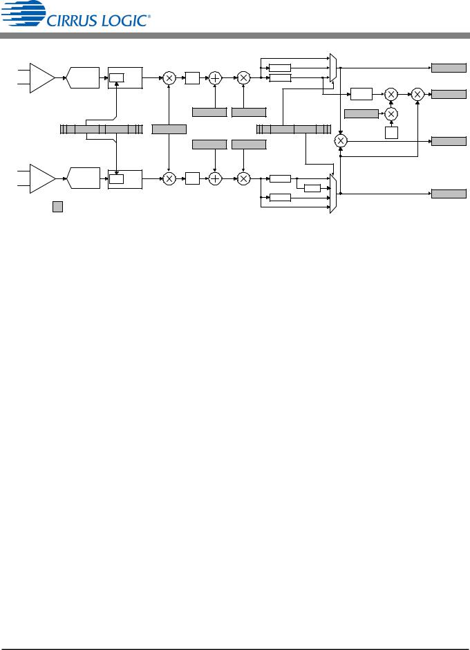
Figure 6. Signal Flow for V, I, P, and Q Measurements
4. SIGNAL FLOW DESCRIPTION
The signal flow for voltage, current measurement, and the other calculations is shown in Figure 6.
The signal flow consists of a current and a voltage channel. The current and voltage channels have differential input pins.
4.1 Analog-to-Digital Converters
Both input channels use fourth-order delta-sigma modulators to convert the analog inputs to single-bit digital data streams. The converters sample at a rate of MCLK/8. This high sampling provides a wide dynamic range and simplifies anti-alias filter design.
4.2 Decimation Filters
The single-bit modulator output data is widened to 24 bits and down sampled to MCLK/1024 with low-pass decimation filters. These decimation filters are third-order Sinc filters. The filter outputs pass through an IIR "anti-sinc" filter.
4.3 IIR Filter
The IIR filter is used to compensate for the amplitude roll-off of the decimation filters. The droop-correction filter flattens the magnitude response of the channel out to the Nyquist frequency, thus allowing for accurate measurements of up to 2kHz (MCLK = 4.096MHz). By default, the IIR filters are enabled. The IIR filters can be bypassed by setting the IIR_OFF bit in the Config2 register.
4.4 Phase Compensation
Phase compensation changes the phase of voltage relative to current by adding a delay in the decimation filters. The amount of phase shift is set by the PC register bits CPCC[1:0] and FPCC[8:0] for the current channel. For the voltage channel, only bits CPCC[1:0] affect the delay.
Fine phase compensation control bits, FPCC[8:0], provide up to 1/OWR delay in the current channel. Coarse phase compensation control bits, CPCC[1:0], provide an additional 1/OWR delay in the current channel or up to 2/OWR delay in the voltage channel. Negative delay in the voltage channel can be implemented by setting longer delay in the current channel than the voltage channel. For a OWR of 4000Hz, the delay range is ±500µs, a phase shift of ±8.99° at 50Hz and ±10.79° at 60Hz. The step size is 0.008789° at 50Hz and 0.010547° at 60Hz. For more information about phase compensation, see section 7.2 Phase Compensation on page 53.
4.5 DC Offset & Gain Correction
The system and CS5490 inherently have component tolerances, gain, and offset errors, which can be removed using the gain and offset registers. Each measurement channel has its own set of gain and offset registers. For every instantaneous voltage and current sample, the offset and gain values are used to correct DC offset and gain errors in the channel (see section 7. System Calibration on page 52 for more details).
DS982F3 |
15 |
CS5490
4.6 High-pass & Phase Matching Filters
Optional high-pass filters (HPF in Figure 6) remove any DC component from the selected signal paths. Each power calculation contains a current and voltage channel. If an HPF is enabled in only one channel, a phase-matching filter (PMF) should be applied to the other channel to match the phase response of the HPF. For AC power measurement, high-pass filters should be enabled on the voltage and current channels. For information about how to enable and disable the HPF or PMF on each channel, refer to Config2 register descriptions in section 6.6 Register Descriptions on page 32.
4.7 Digital Integrators
Optional digital integrators (INT in Figure 6) are implemented on the current channel to compensate for the 90° phase shift and 20dB/decade gain generated by the Rogowski coil current sensor. When a Rogowski coil is used as the current sensor, the integrator (INT) should be enabled on that current channel. For information about how to enable and disable the INT on the current channel, refer to Config2 register descriptions in section 6.6 Register Descriptions on page 32.
4.8 Low-rate Calculations
All the RMS and power results come from low-rate calculations by averaging the output word rate (OWR) instantaneous values over N samples, where N is the value stored in the SampleCount register. The low-rate interval or averaging period is N divided by OWR (4000Hz if MCLK = 4.096MHz). The CS5490 provides
V |
N |
÷ N |
|
|
|
|
|
|
IACOFF |
||
I |
N |
÷ N |
+ |
- |
|
|
|
|
|
||
|
|
|
QOFF |
||
|
N |
|
+ |
+ |
|
Q |
|
÷ N |
|
||
|
|||||
|
|
|
|
||
|
|
|
POFF |
||
|
N |
|
+ |
+ |
|
P |
|
÷ N |
|
||
|
|||||
|
|
|
|
||
|
Registers |
|
|
|
|
two averaging modes for low-rate calculations: Fixed Number of Sample Averaging mode and Line-cycle Synchronized Averaging mode. By default, the CS5490 averages with the Fixed Number of Samples Averaging mode. By setting the AVG_MODE bit in the Config2 register, the CS5490 will use the Line-cycle Synchronized Averaging mode.
4.8.1 Fixed Number of Samples Averaging
N is the preset value in the SampleCount register and should not be set less than 100. By default, the SampleCount register is 4000. With MCLK = 4.096 MHz, the averaging period is fixed at N/4000 = 1 second, regardless of the line frequency.
4.8.2 Line-cycle Synchronized Averaging
When operating in Line-cycle Synchronized Averaging mode, and when line frequency measurement is enabled (see section 5.4 Line Frequency Measurement on page 19), the CS5490 uses the voltage (V) channel zero crossings and measured line frequency to automatically adjust N such that the averaging period will be equal to the number of half line-cycles in the CycleCount register. For example, if the line frequency is 51Hz, and the CycleCount register is set to 100, N will be 4000 (100/2)/51 = 3921 during continuous conversion. N is self-adjusted according to the line frequency, therefore the averaging period is always close to the whole number of half line-cycles, and the low-rate calculation results will minimize ripple and maximize resolution, especially when the line frequency varies. Before starting a low-rate conversion in the Line-cycle Synchronized Averaging mode, the
VRMS |
|
|
Config 2 |
||
|
|
|
|
|
|
|
|
|
... |
APCM |
... |
IRMS |
|
|
|
MUX |
S |
QAVG |
|
|
X |
|
|
|
|
Inverse |
PAVG |
+ + |
|
X |
|
 X
X
PF
Figure 7. Low-rate Calculations
16 |
DS982F3 |

SampleCount register should not be changed from its default value of 4000, and bit AFC of the Config2 register must be set. During continuous conversion, the host processor should not change the SampleCount register.
4.8.3 RMS Current & Voltage
The root mean square (RMS in Figure 7) calculations are performed on N instantaneous voltage and current samples using Equation 1:
|
N – 1 |
|
N – 1 |
IRMS = |
I2n |
VRMS = |
V2n [Eq.1] |
n = 0 |
n = 0 |
||
|
------------------- |
|
--------------------- |
|
N |
|
N |
4.8.4 Active Power
The instantaneous voltage and current samples are multiplied to obtain the instantaneous power (P) (see Figure 6). The product is then averaged over N samples to compute active power (PAVG).
4.8.5 Reactive Power
Instantaneous reactive power (Q) is the sample rate result obtained by multiplying instantaneous current (I) by instantaneous quadrature voltage (Q). These values are created by phase shifting instantaneous voltage (V) 90° using first-order integrators (see Figure 6). The gain of these integrators is inversely related to line frequency, so their gain is corrected by the Epsilon register, which is based on line frequency. Reactive power (QAVG) is generated by integrating the instantaneous quadrature power over N samples.
4.8.6 Apparent Power
By default, the CS5490 calculates the apparent power (S) as the product of RMS voltage and current. See Equation 2:
S = VRMS IRMS |
[Eq.2] |
The CS5490 also provides an alternate apparent power calculation method. The alternate apparent power method uses real power (PAVG) and reactive power (QAVG) to calculate apparent power. See Equation 3.
S = QAVG2 + PAVG2 |
[Eq.3] |
CS5490
The APCM bit in the Config2 register controls which method is used for apparent power calculation.
4.8.7 Peak Voltage & Current
Peak current (IPEAK) and peak voltage (VPEAK) are calculated over N samples and recorded in the corre-
sponding channel peak register documented in the register map. This peak value is updated every N samples.
4.8.8 Power Factor
Power factor (PF) is active power divided by apparent power, as shown below. The sign of the power factor is determined by the active power. See Equation 4.
PF = |
P---------------------ACTIVE- |
[Eq.4] |
|
S |
|
4.9 Average Active Power Offset
The average active power offset register, POFF, can be used to offset erroneous power sources resident in the system not originating from the power line. Residual power offsets are usually caused by crosstalk into the current channel from the voltage channel, or from ripple on the meter’s or chip’s power supply, or from inductance from a nearby transformer.
These offsets can be either positive or negative, indicating crosstalk coupling either in phase or out of phase with the applied voltage input. The power offset register can compensate for either condition.
To use this feature, measure the average power at no load and take the measured result (from the PAVG register), invert (negate) the value, and write it to the associated power offset register, POFF.
4.10 Average Reactive Power Offset
The average reactive power offset register, QOFF, can be used to offset erroneous power sources resident in the system not originating from the power line. Residual reactive power offsets are usually caused by crosstalk into the current channel from the voltage channel, or from ripple on the meter’s or chip’s power supply, or from inductance from a nearby transformer.
These offsets can be either positive or negative, depending on the phase angle between the crosstalk coupling and the applied voltage. The reactive power offset register can compensate for either condition. To use this feature, measure the average reactive power at no load. Take the measured result from the QAVG register, invert (negate) the value and write it to the reactive power offset register, QOFF.
DS982F3 |
17 |
5. FUNCTIONAL DESCRIPTION
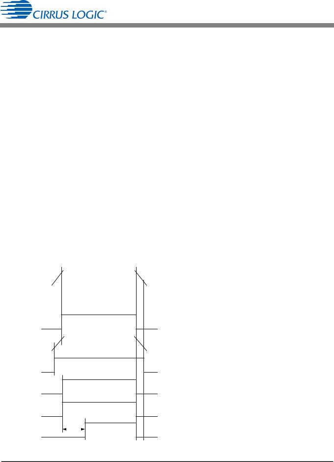
5.1 Power-on Reset (POR)
The CS5490 has an internal power supply supervisor circuit that monitors the VDDA and VDDD power supplies and provides the master reset to the chip. If any of these voltages are in the reset range, the master reset is triggered.
Both the analog and the digital supply have their own POR circuit. During power-up, both supplies have to be above the rising threshold for the master reset to be de-asserted.
Each POR is divided into 2 blocks: rough and fine. Rough POR triggers the fine POR. Rough POR depends only on the supply voltage. The trip point for the fine POR is dependent on bandgap voltage for precise control.
The POR circuit also acts as a brownout detect. The fine POR detects supply drops and asserts the master reset.
The rough and fine PORs have hysteresis in their rise and fall thresholds which prevents the reset signal from chattering.
The following plot shows the POR outputs for each of the power supplies. The POR_Fine_VDDA and POR_Fine_VDDD signals are AND-ed to form the actual power-on reset signal to the digital circuity. The digital circuitry, in turn, holds the master reset signal for 130ms and then de-asserts the master reset.
VDDA |
|
|
|
|
|
|
Vth2 |
|
|
Vth5 |
|||||
|
|
|
|
|
|
|
|
||||||||
|
|
|
|
|
|
||||||||||
Vth1 |
|
|
|
|
|
|
|
|
|
|
Vth6 |
||||
|
|
|
|
|
|
|
|
|
|
|
|
|
|||
|
|
|
|
|
|
|
|
|
|
|
|
|
|
|
|
POR_Rough_VDDA |
|
|
|
|
|
|
|
|
|
|
|
|
|
|
|
|
|
|
|
|
|
|
|
|
|
|
|
|
|
||
|
|
|
|
|
|
|
|
|
|
|
|
|
|
|
|
|
|
|
|
|
|
|
|
|
|
|
|
|
|
|
|
POR_Fine_VDDA
|
|
|
|
|
|
|
Vth4 |
Vth7 |
|
|
|
|
|
|
|
|
|
|
|
|
|
|
|
||||||
VDDD |
|
|
|
|
|
|
Vth8 |
|||||||
|
|
|
|
Vth3 |
|
|
|
|
|
|
||||
|
|
|
|
|
|
|
|
|
||||||
|
|
|
|
|||||||||||
POR_Rough_VDDD
POR_Fine_VDDD
POR_Fine_VDDA
POR_Fine_VDDD
Master Reset |
|
130ms |
|
|
|
||
|
|
|
|
Figure 8. Power-on Reset Timing
CS5490
Table 1. POR Thresholds
Typical POR |
Rising |
Falling |
||
Threshold |
||||
|
|
|||
VDDA |
Rough |
Vth1 = 2.34V |
Vth6 = 2.06V |
|
Fine |
Vth2 = 2.77V |
Vth5 = 2.59V |
||
|
||||
VDDD |
Rough |
Vth3 = 1.20V |
Vth8 = 1.06V |
|
Fine |
Vth4 = 1.51V |
Vth7 = 1.42V |
||
|
||||
5.2 Power Saving Modes
Power Saving modes for CS5490 are accessed through the Host Instruction Commands (see 6.1 Host Commands on page 24).
•Standby: Powers down all the ADCs, rough buffer, and the temperature sensor. Standby mode disables the system time calculations. Use the wake-up command to come out of standby mode.
•Wake-up: Clears the ADC power-down bits and starts the system time calculations.
After any of these commands are completed, the DRDY bit is set in the Status0 register.
5.3 Zero-crossing Detection
Zero-crossing detection logic is implemented in CS5490. A low-pass filter can be enabled by setting ZX_LPF bit in register Config2. The low-pass filter has a cut-off frequency of 80Hz. It is used to eliminate any harmonics and to help the zero-crossing detection on the 50Hz or 60Hz fundamental component. The zero-crossing level registers are used to set the minimum threshold over which the channel peak has to exceed in order for the zero-crossing detection logic to function. There are two separate zero-crossing level
registers: VZXLEVEL is the threshold for the voltage channels, and IZXLEVEL is the threshold for the current channels.
18 |
DS982F3 |
Loading...