


CS4226
Surround Sound Codec
Features
lStereo 20-bit A/D Converters
lSix 20-bit D/A Converters
lS/PDIF Receiver
— AC-3 & MPEG Auto-detect Capability
l108 dB DAC Signal-to-Noise Ratio (EIAJ)
lMono 20-bit A/D Converter
lProgrammable Input Gain & Output Attenuation
lOn-chip Anti-aliasing and Output Smoothing Filters
lDe-emphasis for 32 kHz, 44.1 kHz, 48 kHz
I
Description
The CS4226 is a single-chip codec providing stereo an- alog-to-digital and six digital-to-analog converters using delta-sigma conversion techniques. This +5 V device also contains volume control independently selectable for each of the six D/A channels. An S/PDIF receiver is included as a digital input channel. Applications include Dolby Pro-logic, THX, DTS and Dolby Digital AC-3 home theater systems, DSP based car audio systems, and other multi-channel applications.
The CS4226 is packaged in a 44-pin plastic TQFP.
ORDERING INFORMATION |
|
|
CS4226-KQ |
-10° to +70° C |
44-pin TQFP |
CS4226-BQ |
-40° to +85° C |
44-pin TQFP |
CDB4226 |
|
Evaluation Board |
|
SCL/CCLK SDA/CDOUT AD1/CDIN AD0/CS |
I2C/SPI |
VD+ |
VA+ |
|
||||
PDN |
|
|
Control Port |
|
|
|
Voltage |
CMOUT |
|
|
|
|
|
|
Reference |
||||
|
|
|
|
|
DAC#1 |
Volume |
|
|
AOUT1 |
LRCK |
|
|
|
|
|
Control |
|
|
|
|
|
|
|
DAC#2 |
Volume |
|
|
|
|
SCLK |
|
|
|
|
|
|
AOUT2 |
||
|
|
|
|
|
Control |
Analog Low Pass and |
|
|
|
SDIN1 |
|
|
|
|
|
|
|
||
Audio Data Interface |
|
|
Digital Filters |
DAC#3 |
Volume |
Output Stage |
AOUT3 |
||
SDIN2 |
|
|
|||||||
|
|
|
Control |
|
|||||
SDIN3 |
|
|
|
|
|||||
|
|
DAC#4 |
Volume |
AOUT4 |
|||||
|
|
|
|||||||
|
|
|
|
Control |
|
||||
|
|
|
DAC#5 |
Volume |
AOUT5 |
||||
|
|
|
|
Control |
|||||
|
|
|
|
|
|||||
SDOUT1 |
Serial |
|
|
|
DAC#6 |
Volume |
|
|
AOUT6 |
SDOUT2 |
|
|
|
|
Mono |
Control |
|
|
|
|
|
|
Digital Filters |
|
|
|
AINAUX |
||
|
|
|
ADC |
|
|
|
|||
OVL/ERR |
|
|
|
|
|
|
|||
|
|
MUX |
Left |
|
Input Gain |
|
AIN1L |
||
|
|
|
|
Input MUX |
AIN1R |
||||
|
|
|
|
ADC |
|
||||
|
|
|
|
Right |
|
AIN2L/FREQ0 |
|||
DEM |
DEM |
|
|
ADC |
|
AIN2R/FREQ1 |
|||
|
|
|
|
AIN3L/AUTODATA |
|||||
|
|
|
|
|
|
|
|
|
|
|
|
Clock Osc/ |
PLL |
S/PDIF RX/Auxiliary Input |
AIN3R/AUDIO |
||||
|
|
AGND1 |
|||||||
|
|
Divider |
|
|
|
|
|
||
|
|
|
|
|
|
|
|
|
AGND2 |
|
CLKOUT |
XTI |
XTO |
FILT HOLD/RUBIT |
LRCKAUX/RX3 |
RX1 DGND1 DGND2 |
|||
|
|
|
|
|
DATAUX/RX4 |
SCLKAUX/RX2 |
|
||
Cirrus Logic, Inc. |
Copyright ã Cirrus Logic, Inc. 1998 |
|
Crystal Semiconductor Products Division |
SEP ‘98 |
|
P.O. Box 17847, Austin, Texas 78760 |
(All Rights Reserved) |
DS188F1 |
|
(512) 445 7222 FAX: (512) 445 7581 |
1 |
|
http://www.crystal.com |
||
|

CS4226
TABLE OF CONTENTS |
|
CHARACTERISTICS/SPECIFICATIONS ............................................................ |
3 |
ANALOG CHARACTERISTICS................................................................... |
3 |
SWITCHING CHARACTERISTICS ............................................................. |
5 |
SWITCHING CHARACTERISTICS - CONTROL PORT ............................. |
6 |
S/PDIF RECEIVER CHARACTERISTICS................................................... |
7 |
ABSOLUTE MAXIMUM RATINGS .............................................................. |
8 |
RECOMMENDED OPERATING CONDITIONS .......................................... |
8 |
DIGITAL CHARACTERISTICS.................................................................... |
8 |
FUNCTIONAL DESCRIPTION .......................................................................... |
10 |
Overview ................................................................................................... |
10 |
Analog Inputs ............................................................................................ |
10 |
Line Level Inputs ................................................................................ |
10 |
Adjustable Input Gain ......................................................................... |
11 |
High Pass Filter .................................................................................. |
11 |
Analog Outputs ......................................................................................... |
11 |
Line Level Outputs ............................................................................. |
11 |
Output Level Attenuator ..................................................................... |
11 |
Clock Generation ...................................................................................... |
12 |
Clock Source ...................................................................................... |
12 |
Master Clock Output .......................................................................... |
13 |
Synchronization .................................................................................. |
13 |
Digital Interfaces ....................................................................................... |
13 |
Audio DSP Serial Interface Signals .................................................... |
13 |
Audio DSP Serial Interface Formats .................................................. |
13 |
Auxiliary Audio Port Signals ............................................................... |
15 |
Auxiliary Audio Port Formats .............................................................. |
15 |
S/PDIF Receiver ................................................................................ |
15 |
AC-3/MPEG Auto Detection ............................................................... |
16 |
Control Port Signals .................................................................................. |
16 |
SPI Mode ........................................................................................... |
16 |
I2C Mode ............................................................................................ |
17 |
Control Port Bit Definitions ................................................................. |
17 |
Power-up/Reset/Power Down Mode ......................................................... |
18 |
DAC Calibration ........................................................................................ |
18 |
De-Emphasis ............................................................................................ |
18 |
HOLD Function ......................................................................................... |
19 |
Power Supply, Layout, and Grounding ..................................................... |
19 |
ADC and DAC Filter Response Plots ....................................................... |
19 |
REGISTER DESCRIPTION ............................................................................... |
21 |
PIN DESCRIPTION ............................................................................................ |
29 |
PARAMETER DEFINITIONS ............................................................................. |
34 |
PACKAGE DIMENSIONS .................................................................................. |
35 |
Advanced product information describes products which are in development and subject to development changes. Cirrus Logic, Inc. has made best efforts to ensure that the information contained in this document is accurate and reliable. However, the information is subject to change without notice and is provided “AS IS” without warranty of any kind (express or implied). No responsibility is assumed by Cirrus Logic, Inc. for the use of this information, nor for infringements of patents or other rights of third parties. This document is the property of Cirrus Logic, Inc. and implies no license under patents, copyrights, trademarks, or trade secrets. No part of this publication may be copied, reproduced, stored in a retrieval system, or transmitted, in any form or by any means (electronic, mechanical, photographic, or otherwise). Furthermore, no part of this publication may be used as a basis for manufacture or sale of any items without the prior written consent of Cirrus Logic, Inc. The names of products of Cirrus Logic, Inc. or other vendors and suppliers appearing in this document may be trademarks or service marks of their respective owners which may be registered in some jurisdictions. A list of Cirrus Logic, Inc. trademarks and service marks can be found at http://www.cirrus.com.
Dolby and AC-3 are registered trademarks, Dolby Pro-Logic is a trademark of Dolby Laboratories Licensing Corporation. DTS is a registered trademark of DTS, Inc.. THX is a registered trademark of LucasArts Entertainment Company. I2C is a registered trademark of Philips Semiconductor.
2 |
DS188F1 |

CS4226
CHARACTERISTICS/SPECIFICATIONS
ANALOG CHARACTERISTICS (TA = 25°C; VA+, VD+ = +5V; Full Scale Input Sine wave,
990.52 Hz; Fs = 44.1 kHz (PLL in use); Measurement Bandwidth is 20 Hz to 20 kHz; Local components as shown in Figure 1; SPI mode, Format 3, unless otherwise specified.)
|
|
CS4226-KQ |
CS4226-BQ |
|
||||
|
|
|
|
|
|
|
|
|
Parameter |
Symbol |
Min |
Typ |
Max |
Min |
Typ |
Max |
Units |
|
|
|
|
|
|
|
|
|
Analog Input Characteristics - Minimum gain setting (0 dB) Differential Input; unless otherwise specified.
ADC Resolution |
Stereo Audio channels |
|
16 |
- |
20 |
16 |
- |
20 |
Bits |
|
|
Mono channel |
|
16 |
- |
20 |
16 |
- |
20 |
Bits |
|
|
|
|
|
|
|
|
|
|
|
|
Total Harmonic Distortion |
|
THD |
|
0.003 |
- |
|
0.003 |
- |
% |
|
|
|
|
|
|
|
|
|
|
|
|
Dynamic Range |
(A weighted, Stereo) |
|
92 |
95 |
- |
90 |
93 |
- |
dB |
|
|
(unweighted, Stereo) |
|
- |
92 |
- |
- |
90 |
- |
dB |
|
|
(A weighted, Mono) |
|
89 |
- |
- |
87 |
- |
- |
dB |
|
|
|
|
|
|
|
|
|
|
|
|
Total Harmonic |
-1 dB, Stereo |
(Note 1) |
THD+N |
- |
-88 |
-82 |
- |
-86 |
-80 |
dB |
Distortion + Noise |
-1 dB, Mono |
(Note 1) |
|
- |
- |
-72 |
- |
- |
-70 |
dB |
|
|
|
|
|
|
|
|
|
|
|
Interchannel Isolation |
|
|
- |
90 |
- |
- |
90 |
- |
dB |
|
|
|
|
|
|
|
|
|
|
|
|
Interchannel Gain Mismatch |
|
|
- |
0.1 |
- |
- |
0.1 |
- |
dB |
|
|
|
|
|
|
|
|
|
|
|
|
Programmable Input Gain Span |
|
|
8 |
9 |
10 |
8 |
9 |
10 |
dB |
|
|
|
|
|
|
|
|
|
|
|
|
Gain Step Size |
|
|
|
2.7 |
3 |
3.3 |
2.7 |
3 |
3.3 |
dB |
|
|
|
|
|
|
|
|
|
|
|
Offset Error (with high pass filter) |
|
|
- |
- |
0 |
- |
- |
0 |
LSB |
|
|
|
|
|
|
|
|
|
|
||
Full Scale Input Voltage (Single Ended): |
|
0.90 |
1.0 |
1.10 |
0.90 |
1.0 |
1.10 |
Vrms |
||
|
|
|
|
|
|
|
|
|
|
|
Gain Drift |
|
|
|
- |
100 |
- |
- |
100 |
- |
ppm/°C |
|
|
|
|
|
|
|
|
|
|
|
Input Resistance |
|
(Note 2) |
|
10 |
- |
- |
10 |
- |
- |
kΩ |
Input Capacitance |
|
|
|
- |
- |
15 |
- |
- |
15 |
pF |
|
|
|
|
|
|
|
|
|
|
|
CMOUT Output Voltage |
|
|
- |
2.3 |
- |
- |
2.3 |
- |
V |
|
|
|
|
|
|
|
|
|
|
||
A/D Decimation Filter Characteristics |
|
|
|
|
|
|
|
|
||
|
|
|
|
|
|
|
|
|
|
|
Passband |
|
(Note 3) |
|
0.02 |
- |
20.0 |
0.02 |
- |
20.0 |
kHz |
|
|
|
|
|
|
|
|
|
|
|
Passband Ripple |
|
|
|
- |
- |
0.01 |
- |
- |
0.01 |
dB |
|
|
|
|
|
|
|
|
|
|
|
Stopband |
|
(Note 3) |
|
27.56 |
- |
5617.2 |
27.56 |
- |
5617.2 |
kHz |
|
|
|
|
|
|
|
|
|
|
|
Stopband Attenuation |
(Note 4) |
|
80 |
- |
- |
80 |
- |
- |
dB |
|
|
|
|
|
|
|
|
|
|
|
|
Group Delay (Fs = Output Sample Rate) |
(Note 5) |
tgd |
- |
15/Fs |
- |
- |
15/Fs |
- |
s |
|
Group Delay Variation vs. Frequency |
|
tgd |
- |
- |
0 |
- |
- |
0 |
μs |
|
Notes: 1. Referenced to typical full-scale differential input voltage (2Vrms).
2.Input resistance is for the input selected. Non-selected inputs have a very high (>1MΩ) input resistance. The input resistance will vary with gain value selected, but will always be greater than the min. value specified
3.Filter characteristics scale with output sample rate.
4.The analog modulator samples the input at 5.6448 MHz for an output sample rate of 44.1 kHz. There is no rejection of input signals which are multiples of the sampling frequency (n × 5.6448 MHz ±20.0 kHz where n = 0,1,2,3...).
5.Group delay for Fs = 44.1 kHz, tgd = 15/44.1 kHz = 340 μs
DS188F1 |
3 |

CS4226
ANALOG CHARACTERISTICS (Continued)
|
|
|
|
|
CS4226-KQ |
CS4226-BQ |
|
||||
Parameter |
|
Symbol |
|
|
|
|
|
|
Units |
||
|
Min |
Typ |
Max |
Min |
Typ |
Max |
|||||
|
|
|
|
|
|
|
|
|
|
||
High Pass Filter Characteristics |
|
|
|
|
|
|
|
|
|
||
|
|
|
|
|
|
|
|
|
|
|
|
Frequency Response: |
-3 dB |
(Note 3) |
|
- |
3.4 |
- |
- |
3.4 |
- |
Hz |
|
|
|
-0.13 dB |
|
|
- |
20 |
- |
- |
20 |
- |
Hz |
|
|
|
|
|
|
|
|
|
|
|
|
Phase Deviation |
|
@ 20 Hz |
(Note 3) |
|
- |
10 |
- |
- |
10 |
- |
Deg. |
|
|
|
|
|
|
|
|
|
|
|
|
Passband Ripple |
|
|
|
|
- |
- |
0 |
- |
- |
0 |
dB |
|
|
|
|
|
|
|
|
|
|||
Analog Output Characteristics - Minimum Attenuation, 10 k, 100 pF load; unless otherwise specified. |
|
||||||||||
|
|
|
|
|
|
|
|
|
|
|
|
DAC Resolution |
|
|
|
|
16 |
- |
20 |
16 |
- |
20 |
Bits |
|
|
|
|
|
|
|
|
|
|
|
|
Signal-to-Noise/Idle |
|
(DAC muted, A weighted) |
|
101 |
108 |
- |
99 |
106 |
- |
dB |
|
Channel Noise |
|
|
|
|
|
|
|
|
|
|
|
|
|
|
|
|
|
|
|
|
|
||
Dynamic Range |
(DAC not muted, A weighted) |
|
93 |
98 |
- |
91 |
96 |
- |
dB |
||
|
(DAC not muted, unweighted) |
|
- |
95 |
- |
- |
93 |
- |
dB |
||
|
|
|
|
|
|
|
|
|
|
|
|
Total Harmonic Distortion |
|
|
THD |
- |
0.003 |
- |
- |
0.003 |
- |
% |
|
|
|
|
|
|
|
|
|
|
|
||
Total Harmonic Distortion + Noise |
(Stereo) |
THD+N |
- |
-88 |
-83 |
- |
-86 |
-81 |
dB |
||
|
|
|
|
|
|
|
|
|
|
|
|
Interchannel Isolation |
|
|
|
|
- |
90 |
- |
- |
90 |
- |
dB |
|
|
|
|
|
|
|
|
|
|
||
Interchannel Gain Mismatch |
|
|
- |
0.1 |
- |
- |
0.1 |
- |
dB |
||
|
|
|
|
|
|
|
|
|
|
|
|
Attenuation Step Size |
|
(All Outputs) |
|
0.7 |
1 |
1.3 |
0.7 |
1 |
1.3 |
dB |
|
|
|
|
|
|
|
|
|
|
|||
Programmable Output Attenuation Span |
|
-84 |
-86 |
- |
-84 |
-86 |
- |
dB |
|||
|
|
|
|
|
|
|
|
|
|
|
|
Offset Voltage |
|
(relative to CMOUT) |
|
- |
±15 |
- |
- |
±15 |
- |
mV |
|
|
|
|
|
|
|
|
|
|
|
|
|
Full Scale Output Voltage |
|
|
|
0.92 |
1.0 |
1.08 |
0.92 |
1.0 |
1.08 |
Vrms |
|
|
|
|
|
|
|
|
|
|
|
|
|
Gain Drift |
|
|
|
|
- |
100 |
- |
- |
100 |
- |
ppm/°C |
|
|
|
|
|
|
|
|
|
|
|
|
Out-of-Band Energy |
|
(Fs/2 to 2Fs) |
|
- |
-60 |
- |
- |
-60 |
- |
dBFs |
|
|
|
|
|
|
|
|
|
|
|
|
|
Analog Output Load |
|
|
Resistance: |
|
10 |
- |
- |
10 |
- |
- |
kΩ |
|
|
|
Capacitance: |
|
- |
- |
100 |
- |
- |
100 |
pF |
|
|
|
|
|
|
|
|
|
|||
Combined Digital and Analog Filter Characteristics |
|
|
|
|
|
|
|
|
|||
|
|
|
|
|
|
|
|
|
|
|
|
Frequency Response |
|
10 Hz to 20 kHz |
|
- |
±0.1 |
- |
- |
±0.1 |
- |
dB |
|
|
|
|
|
|
|
|
|
|
|
||
Deviation from Linear Phase |
|
|
- |
±0.5 |
- |
- |
±0.5 |
- |
Deg. |
||
|
|
|
|
|
|
|
|
|
|
||
Passband: to 0.01 dB corner |
(Notes 6, 7) |
|
0 |
- |
20.0 |
0 |
- |
20.0 |
kHz |
||
|
|
|
|
|
|
|
|
|
|
|
|
Passband Ripple |
|
|
(Note 7) |
|
- |
- |
±0.01 |
- |
- |
±0.01 |
dB |
|
|
|
|
|
|
|
|
|
|
|
|
Stopband |
|
|
(Notes 6 ,7) |
|
24.1 |
- |
- |
24.1 |
- |
- |
kHz |
|
|
|
|
|
|
|
|
|
|
|
|
Stopband Attenuation |
|
|
(Note 8) |
|
70 |
- |
- |
70 |
- |
- |
dB |
|
|
|
|
|
|
|
|
|
|
||
Group Delay (Fs = Input Word Rate) |
(Note 5) |
tgd |
- |
16/Fs |
- |
- |
16/Fs |
- |
s |
||
|
|
|
|
|
|
|
|
|
|
||
Analog Loopback Performance |
|
|
|
|
|
|
|
|
|
||
|
|
|
|
|
|
|
|
||||
Signal-to-noise Ratio (CCIR-2K weighted, -20 dB input) |
CCIR-2K |
- |
71 |
- |
- |
71 |
- |
dB |
|||
|
|
|
|
|
|
|
|
|
|
|
|
Power Supply |
|
|
|
|
|
|
|
|
|
|
|
|
|
|
|
|
|
|
|
|
|
|
|
Power Supply Current |
|
Operating |
|
- |
90 |
113 |
- |
90 |
115 |
mA |
|
|
|
|
Power Down |
|
- |
1 |
3 |
- |
1 |
3 |
mA |
|
|
|
|
|
|
|
|
|
|
||
Power Supply Rejection |
(1 kHz, 10 mVrms) |
|
- |
45 |
- |
- |
45 |
- |
dB |
||
Notes: 6. The passband and stopband edges scale with frequency. For input word rates, Fs, other than 44.1 kHz, the 0.01 dB passband edge is 0.4535×Fs and the stopband edge is 0.5465×Fs.
7.Digital filter characteristics.
8.Measurement bandwidth is 10 Hz to 3 Fs.
4 |
DS188F1 |
CS4226
SWITCHING CHARACTERISTICS (TA = 25°C; VA+, VD+ = +5V ±5%, outputs loaded with 30 pF)
|
|
Parameter |
|
Symbol |
Min |
Typ |
Max |
Units |
||
|
|
|
|
|
|
|
|
|
||
|
Audio ADC's & DAC's Sample Rate |
|
Fs |
4 |
- |
50 |
|
kHz |
||
|
|
|
|
|
|
|
|
|
||
|
XTI Frequency |
(XTI = 256, 384, or 512 Fs) |
|
1.024 |
- |
26 |
|
MHz |
||
|
|
|
|
|
|
|
|
|
|
|
|
XTI Pulse Width High |
XTI = 512 Fs |
|
|
10 |
- |
- |
|
ns |
|
|
|
|
XTI = 384 Fs |
|
|
21 |
- |
- |
|
ns |
|
|
|
XTI = 256 Fs |
|
|
31 |
- |
- |
|
ns |
|
|
|
|
|
|
|
|
|
|
|
|
XTI Pulse Width Low |
XTI = 512 Fs |
|
|
10 |
- |
- |
|
ns |
|
|
|
|
XTI = 384 Fs |
|
|
21 |
- |
- |
|
ns |
|
|
|
XTI = 256 Fs |
|
|
31 |
- |
- |
|
ns |
|
|
|
|
|
|
|
|
|
||
|
PLL Clock Recovery Frequency |
RX, XTI, LRCK, LRCKAUX |
|
30 |
- |
50 |
|
kHz |
||
|
|
|
|
|
|
|
|
|
|
|
|
XTI Jitter Tolerance |
|
|
|
- |
500 |
- |
|
ps |
|
|
|
|
|
|
|
|
|
|
|
|
|
PDN |
Low Time |
|
(Note 9) |
|
500 |
- |
- |
|
ns |
|
|
|
|
|
|
|
|
|
|
|
SCLK Falling Edge to SDOUT Output Valid |
(DSCK = 0) |
tdpd |
- |
- |
1 |
+ 20 |
ns |
|||
------------------- |
||||||||||
|
|
|
|
|
|
|
|
(384)Fs |
|
|
|
LRCK edge to MSB valid |
|
|
tlrpd |
- |
- |
40 |
|
ns |
|
|
SDIN Setup Time Before SCLK Rising Edge |
(DSCK=0) |
tds |
- |
- |
25 |
|
ns |
||
|
SDIN Hold Time After SCLK Rising Edge |
(DSCK=0) |
tdh |
- |
- |
25 |
|
ns |
||
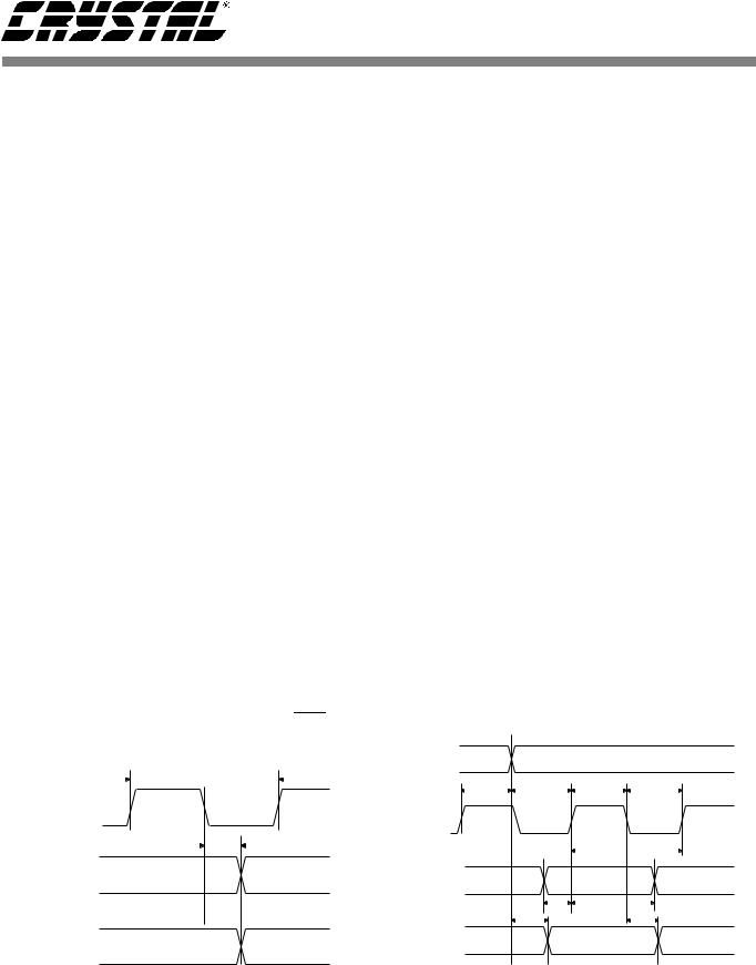
|
Master Mode |
|
|
|
|
|
|
|
|
|
|
|
|
|
|
|
|
|
|
|
|
|
SCLK Period |
|
|
tsck |
1 |
- |
- |
|
ns |
|
|
|
|
------------------- |
|
||||||
|
|
|
|
|
|
(256)Fs |
|
|
|
|
|
SCLK Falling to LRCK Edge |
|
(DSCK=0) |
tmslr |
- |
±10 |
- |
|
ns |
|
|
SCLK Duty Cycle |
|
|
|
- |
50 |
- |
|
% |
|
|
|
|
|
|
|
|
|
|
|
|
|
Slave Mode |
|
|
|
|
|
|
|
|
|
|
|
|
|
|
|
|
|
|
|
|
|
SCLK Period |
|
|
tsckw |
1 |
- |
- |
|
ns |
|
|
|
|
------------------- |
|
||||||
|
|
|
|
|
|
(128)Fs |
|
|
|
|
|
SCLK High Time |
|
|
tsckh |
40 |
- |
- |
|
ns |
|
|
SCLK Low Time |
|
|
tsckl |
40 |
- |
- |
|
ns |
|
|
SCLK Rising to LRCK Edge |
|
(DSCK=0) |
tlrckd |
20 |
- |
- |
|
ns |
|
|
LRCK Edge to SCLK Rising |
|
(DSCK=0) |
tlrcks |
40 |
- |
- |
|
ns |
|
Notes: 9. After powering up the CS4226, PDN should be held low until the power supply is settled.
|
|
|
|
|
|
|
|
|
LRCK |
|
|
|
|
|
|
|
|
|
|
|
|
|
|
|
|
|
t sck |
LRCKAUX |
|
|
|
|
|
|
|
|
|
|
|
|
|
|
|
|
|
(input) |
t lrckd |
t lrcks |
t sckh |
tsckl |
||||||
|
|
|
|
|
|
|
||||||||||||
SCLK* |
|
|||||||||||||||||
|
|
|
|
|
|
|
|
|
|
|||||||||
SCLKAUX* |
SCLK* |
|
|
|
|
|
|
|
|
|
||||||||
(output) |
|
|
|
|
|
|
|
|
|
|||||||||
SCLKAUX* |
|
|
|
|
|
|
|
|
|
|||||||||
|
|
|
|
|
|
|
|
|
|
|
|
|
|
|
|
|
|
|
|
|
|
|
|
|
t mslr |
(input) |
|
|
|
|
|
t sckw |
|
||||
|
|
|
|
|
|
|
|
|
|
|
|
|
||||||
|
|
|
|
|
|
|
|
|
|
|
||||||||
|
|
|
|
|
|
|
|
|
|
|
|
|
|
|||||
LRCK |
SDIN1 |
|
|
|
|
|
|
|
|
|
||||||||
LRCKAUX |
SDIN2 |
|
|
|
|
|
|
|
|
|
||||||||
(output) |
SDIN3 |
|
|
|
|
|
|
|
|
|
||||||||
|
|
|
|
|
|
|
|
|
DATAUX |
|
|
|
|
|
|
|
|
|
|
|
|
|
|
|
|
|
|
|
tlrpd tds |
tdh |
|
|
t |
||||
|
|
|
|
|
|
|
|
|
|
|
|
|
||||||
SDOUT1 |
SDOUT1 |
|
|
|
|
MSB |
|
|
dpd |
|||||||||
|
|
|
|
|
|
MSB-1 |
||||||||||||
SDOUT2 |
SDOUT2 |
|
|
|
|
|
|
|
|
|
||||||||
|
|
|
|
|
|
|
|
|
*SCLK, SCLKAUX shown for DSCK = 0 and ASCK = 0. |
|||||||||
|
|
|
|
|
|
|
|
|
SCLK & SCLKAUX inverted for DSCK = 1 and ASCK = 1, respectively. |
|||||||||
Audio Ports Master Mode Timing |
Audio Ports Slave Mode and Data I/O timing |
|||||||||||||||||
|
|
|
|
|
|
|
|
|
|
|
|
|
|
|
|
|
|
|
DS188F1 |
|
|
|
|
|
|
5 |
|||||||||||
|
|
|
|
|
|
|
|
CS4226 |
||
|
|
|
|
|
|
|
|
|
||
|
|
|
|
|
|
|
|
|
||
|
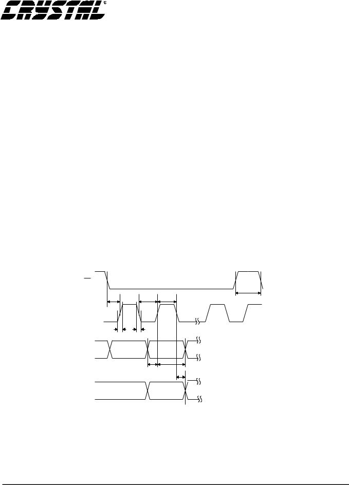
SWITCHING CHARACTERISTICS - CONTROL PORT (TA = 25°C VD+, VA+ = 5V ±5%; |
|||||||||
|
Inputs: logic 0 = DGND, logic 1 = VD+, CL = 30 pF) |
|
|
|
|
|
|
|
||
|
|
|
Parameter |
|
Symbol |
Min |
Max |
|
Units |
|
|
|
|
|
|
|
|
|
|
|
|
|
|
SPI Mode (SPI/I2C = 0) |
|
|
|
|
|
|
|
|
|
|
CCLK Clock Frequency |
|
fsck |
- |
6 |
|
MHz |
|
|
|
|
CS |
High Time Between Transmissions |
|
tcsh |
1.0 |
|
|
μs |
|
|
|
CS |
Falling to CCLK Edge |
|
tcss |
20 |
|
|
ns |
|
|
CCLK Low Time |
|
tscl |
66 |
|
|
ns |
|
||
|
CCLK High Time |
|
tsch |
66 |
|
|
ns |
|
||
|
CDIN to CCLK Rising Setup Time |
|
tdsu |
40 |
|
|
ns |
|
||
|
CCLK Rising to DATA Hold Time |
(Note 10) |
tdh |
15 |
|
|
ns |
|
||
|
CCLK Falling to CDOUT stable |
|
tpd |
|
45 |
|
ns |
|
||
|
|
Rise Time of CDOUT |
|
tr1 |
|
25 |
|
ns |
|
|
|
|
Fall Time of CDOUT |
|
tf1 |
|
25 |
|
ns |
|
|
|
|
Rise Time of CCLK and CDIN |
(Note 11) |
tr2 |
|
100 |
|
ns |
|
|
|
Fall Time of CCLK and CDIN |
(Note 11) |
tf2 |
|
100 |
|
ns |
|
||
Notes: 10. Data must be held for sufficient time to bridge the transition time of CCLK. 11. For FSCK < 1 MHz
CS |
|
|
|
|
|
t css |
t |
scl |
t |
sch |
t csh |
|
|
|
|||
CCLK |
|
|
|
|
|
t r2 |
|
t f2 |
|
|
|
CDIN |
|
|
|
|
|
t dsu t dh |
t pd |
CDOUT
6 |
DS188F1 |
CS4226
SWITCHING CHARACTERISTICS - CONTROL PORT (TA = 25°C; VD+, VA+ = 5V ±5%;
Inputs: logic 0 = DGND, logic 1 = VD+, CL = 30 pF)
|
Parameter |
|
|
|
|
|
|
|
|
|
|
|
Symbol |
|
|
Min |
|
Max |
Units |
||||||||||||||
|
|
|
|
|
|
|
|
|
|
|
|
|
|
|
|
|
|
|
|
|
|
|
|
|
|
|
|
|
|
|
|
|
|
I2C® Mode (SPI/I2C = 1) |
|
|
|
|
|
(Note 12) |
|
|
|
|
|
|
|
|
|
|
|
|
|
|
|
|
|
||||||||||
SCL Clock Frequency |
|
|
|
|
|
|
|
|
|
|
|
fscl |
|
- |
|
|
|
|
|
100 |
kHz |
||||||||||||
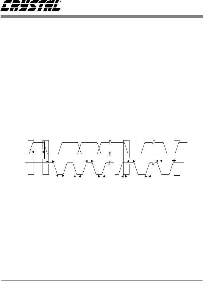
Bus Free Time Between Transmissions |
|
|
|
|
|
|
|
|
tbuf |
|
4.7 |
|
|
|
|
|
|
|
|
μs |
|||||||||||||
Start Condition Hold Time (prior to first clock pulse) |
thdst |
|
4.0 |
|
|
|
|
|
|
|
|
μs |
|||||||||||||||||||||
Clock Low Time |
|
|
|
|
|
|
|
|
|
|
|
|
|
|
|
|
tlow |
|
4.7 |
|
|
|
|
|
|
|
|
μs |
|||||
Clock High Time |
|
|
|
|
|
|
|
|
|
|
|
|
|
|
|
|
thigh |
|
4.0 |
|
|
|
|
|
|
|
|
μs |
|||||
Setup Time for Repeated Start Condition |
|
|
|
|
|
|
|
|
tsust |
|
4.7 |
|
|
|
|
|
|
|
|
μs |
|||||||||||||
SDA Hold Time from SCL Falling |
|
|
|
|
|
(Note 13) |
thdd |
|
0 |
|
|
|
|
|
|
|
|
μs |
|||||||||||||||
SDA Setup Time to SCL Rising |
|
|
|
|
|
|
|
|
|
|
|
tsud |
|
250 |
|
|
|
|
|
|
|
ns |
|||||||||||
Rise Time of Both SDA and SCL Lines |
|
|
|
|
|
|
|
|
|
tr |
|
|
|
|
|
|
|
|
|
1 |
μs |
||||||||||||
Fall Time of Both SDA and SCL Lines |
|
|
|
|
|
|
|
|
|
|
|
|
tf |
|
|
|
|
|
|
|
|
|
300 |
ns |
|||||||||
Setup Time for Stop Condition |
|
|
|
|
|
|
|
|
|
|
|
tsusp |
|
4.7 |
|
|
|
|
|
|
|
|
μs |
||||||||||
Notes: 12. I2C is a registered trademark of Philips Semiconductors. |
|
|
|
|
|
|
|
|
|
|
|
|
|||||||||||||||||||||
13. Data must be held for sufficient time to bridge the 300 ns transition time of SCL. |
|
|
|
|
|||||||||||||||||||||||||||||
Stop |
Start |
|
|
|
|
|
|
|
|
|
|
|
Repeated |
|
|
|
|
|
|
|
|
Stop |
|
||||||||||
|
|
|
|
|
|
|
|
|
|
|
Start |
|
|
|
|
|
|
|
|
|
|||||||||||||
SDA |
|
|
|
|
|
|
|
|
|
|
|
|
|
|
|
|
|
|
|
|
|
|
|
|
|
|
|
|
|
|
|
|
|
|
|
|
|
|
|
|
|
|
|
|
|
|
|
|
|
|
|
|
|
|
|
|
|
|
|
|
|
|
|
|
|
|
|
|
|
|
|
|
|
|
|
|
|
|
|
|
|
|
|
|
|
|
|
|
|
|
|
|
|
|
|
|
|
|
|
|
|
|
|
|
|
|
|
|
|
|
|
|
|
|
|
|
|
|
|
|
|
|
|
|
|
|
|
|
|
|
|
|
|
|
|
t buf |
|
t |
hdst |
|
|
|
t |
high |
|
|
|
|
|
|
t hdst |
|
|
|
t f |
|
|
|
|
|
t susp |
|
|||||||
|
|
|
|
|
|
|
|
|
|
|
|||||||||||||||||||||||
SCL |
|
|
|
|
|
|
|
|
|
|
|
|
|
|
|
|
|
|
|
|
|
|
|
|
|
|
|
|
|
|
|
|
|
|
|
|
|
|
|
|
|
|
|
|
|
|
|
|
|
|
|
|
|
|
|
|
|
|
|
|
|
|
|
|
|
|
|
|
|
|
|
|
|
|
|
|
|
|
|
|
|
|
|
|
|
|
|
|
|
|
|
|
|
|
|
|
|
|
|
||
|
|
|
|
|
|
|
|
|
|
|
|
|
|
|
|
|
|
|
|
|
|
|
|
|
|
|
|
|
|
|
|
|
|
|
|
|
|
|
|
|
|
|
|
|
|
|
|
|
|
|
|
|
|
|
|
|
|
|
|
|
|
|
|
|
|
|
|
|
|
|
t low |
t hdd |
|
|
|
|
|
t sud |
tsust |
t r |
|
|
|
|
|||||||||||||||||
S/PDIF RECEIVER CHARACTERISTICS (RX1, RX2, RX3, RX4 pins only; VD+, VA+ = 5V ±5%)
Parameter |
|
Symbol |
Min |
Typ |
Max |
Units |
|
|
|
|
|
|
|
Input Resistance |
|
ZN |
- |
10 |
- |
kΩ |
Input Voltage |
|
VTH |
200 |
- |
- |
mVpp |
Input Hysteresis |
|
VHYST |
- |
50 |
- |
mV |
Input Sample Frequency |
|
FS |
30 |
- |
50 |
kHz |
CLKOUT Jitter |
(Note 14) |
|
- |
200 |
- |
ps RMS |
|
|
|
|
|
|
|
CLKOUT Duty Cycle (high time/cycle time) |
(Note 15) |
|
40 |
50 |
60 |
% |
|
|
|
|
|
|
|
Notes: 14. CLKOUT Jitter is for 256×FS selected as output frequency measured from falling edge to falling edge. Jitter is greater for 384×Fs and 512×Fs as selected output frequency.
15. For CLKOUT frequency equal to 1×Fs, 384×Fs, and 512×Fs. See Master Clock Output section.
DS188F1 |
7 |

|
|
|
|
|
|
CS4226 |
|||
|
|
|
|
|
|
|
|
|
|
|
|
|
|
|
|
|
|
|
|
|
ABSOLUTE MAXIMUM RATINGS (AGND, DGND = 0 V, all voltages with respect to 0 V.) |
|
|
||||||
|
|
|
|
|
|
|
|
|
|
|
|
Parameter |
Symbol |
Min |
Typ |
Max |
|
Units |
|
|
|
|
|
|
|
|
|
|
|
|
Power Supplies |
Digital |
VD+ |
-0.3 |
- |
6.0 |
|
V |
|
|
|
Analog |
VA+ |
-0.3 |
- |
6.0 |
|
V |
|
|
|
|
|
|
|
|
|
|
|
|
Input Current |
(Note 16) |
|
- |
- |
±10 |
|
mA |
|
|
|
|
|
|
|
|
|
|
|
|
Analog Input Voltage |
(Note 17) |
|
-0.7 |
- |
(VA+)+0.7 |
|
V |
|
|
|
|
|
|
|
|
|
|
|
|
Digital Input Voltage |
(Note 17) |
|
-0.7 |
- |
(VD+)+0.7 |
|
V |
|
|
|
|
|
|
|
|
|
|
|
|
Ambient Temperature |
(Power Applied) |
|
-55 |
- |
+125 |
|
°C |
|
|
|
|
|
|
|
|
|
|
|
|
Storage Temperature |
|
|
-65 |
- |
+150 |
|
°C |
|
|
|
|
|
|
|
|
|
|
|
Notes: 16. Any pin except supplies. Transient currents of up to ±100 mA on the analog input pins will not cause SCR latch-up.
17. The maximum over or under voltage is limited by the input current.
Warning: Operation at or beyond these limits may result in permanent damage to the device. Normal operation is not guaranteed at these extremes.
RECOMMENDED OPERATING CONDITIONS (AGND, DGND = 0 V, all voltages with respect to 0 V.)
Parameter |
|
Symbol |
Min |
Typ |
Max |
Units |
|
|
|
|
|
|
|
Power Supplies |
Digital |
VD+ |
4.75 |
5.0 |
5.25 |
V |
|(VA+)-(VD+)|<0.4 V |
Analog |
VA+ |
4.75 |
5.0 |
5.25 |
V |
|
|
|
|
|
|
|
Operating Ambient Temperature |
CS4226-KQ |
TA |
-10 |
25 |
70 |
°C |
|
CS4226-BQ |
|
-40 |
25 |
85 |
°C |
|
|
|
|
|
|
|
DIGITAL CHARACTERISTICS (TA = 25 °C; VA+, VD+ = 5 V ±5%)
|
Parameter |
Symbol |
Min |
Typ |
Max |
Units |
|
|
|
|
|
|
|
High-level Input Voltage |
(except RX1) |
VIH |
2.8 |
- |
(VD+)+0.3 |
V |
Low-level Input Voltage |
(except RX1) |
VIL |
-0.3 |
- |
0.8 |
V |
High-level Output Voltage at I0 = -2.0 mA |
VOH |
(VD+)-1.0 |
- |
- |
V |
|
Low-level Output Voltage at I0 = 2.0 mA |
VOL |
- |
- |
0.4 |
V |
|
Input Leakage Current |
(Digital Inputs) |
|
- |
- |
10 |
μA |
|
|
|
|
|
|
|
Output Leakage Current |
(High-Impedance Digital Outputs) |
|
- |
- |
10 |
μA |
|
|
|
|
|
|
|
8 |
DS188F1 |
CS4226
Ferrite Bead |
2.0 |
Ω |
|
+5V |
|
||
+ 1 μF 0.1 μF |
+ 1 μF 0.1 μF |
|
|
Supply |
|
||
|
19 |
40 |
|
|
VA+ |
VD+ |
|
To Optional |
16 |
21 |
ANALOG |
CMOUT |
AOUT1 |
FILTER |
|
Input and 1 μF |
+ |
|
|
|
|
||
Output Buffers |
|
|
|
|
|
|
|
|
|
|
|
|
|
22 |
ANALOG |
|
|
10 μF |
* |
14 |
|
|
|
|
|
|
AOUT2 |
FILTER |
|
|
AIN1L |
|
|
|
|
|
|
|||||
|
|
|
|
|
|
|
|
|
|
|
||
Buffer |
10 μF |
* |
13 |
AIN1R |
|
CS4226 |
|
|
|
|
||
|
|
|
|
|
|
|
|
|||||
|
|
|
|
|
|
|
23 |
ANALOG |
||||
|
|
|
|
|
|
|
|
|
||||
|
10 μF |
* |
11 |
|
|
|
|
|
|
AOUT3 |
FILTER |
|
Input |
AIN2L/FREQ0 |
|
|
|
|
|
||||||
|
|
|
|
|
|
|
|
|
||||
10 μF |
|
12 |
|
|
|
|
|
|
|
|
|
|
Optional |
* |
AIN2R/FREQ1 |
|
|
|
AOUT4 |
|
|
||||
|
|
|
|
|
|
|
|
|||||
|
|
|
|
|
|
|
|
|
|
|||
|
10 μF |
|
10 |
|
|
|
|
|
|
24 |
ANALOG |
|
From |
* |
AIN3L/AUTODATA |
|
|
|
FILTER |
|
|||||
|
|
|
|
|
|
|
|
|||||
10 μF |
* |
9 |
|
|
|
|
|
|
|
|
|
|
|
AIN3R/AUDIO |
|
|
|
|
|
|
|||||
|
|
|
|
|
|
|
|
|
|
|||
|
|
|
|
|
|
|
|
|
|
25 |
ANALOG |
|
|
10 μF |
* |
15 |
|
|
|
|
|
|
AOUT5 |
FILTER |
|
|
AINAUX |
|
|
|
|
|
|
|||||
|
|
|
|
|
|
|
|
|
|
|
||
|
RS |
|
27 |
DEM |
|
|
|
|
|
|
|
|
|
RS |
|
2 |
|
|
|
|
|
|
|
|
|
|
|
HOLD/RUBIT |
|
|
|
26 |
ANALOG |
|||||
|
|
|
|
|
|
|
||||||
|
RS |
|
42 |
|
|
|
|
|
|
|||
|
|
RX1 |
|
|
|
|
|
AOUT6 |
FILTER |
|
||
|
|
|
|
|
|
|
|
|
|
|
||
|
100 pF |
|
† |
|
|
|
|
|
|
|
|
|
Digital |
|
|
|
|
|
|
|
|
|
|
|
|
RS |
|
|
|
|
|
|
|
|
3 |
|
|
|
Audio |
|
1 |
DATAUX/RX4 |
|
|
SCL/CCLK |
|
|
||||
Source |
|
|
|
|
|
|
4 |
|
|
|||
100 pF |
|
† |
|
|
|
|
|
SDA/CDOUT |
Microcontroller |
|||
|
|
|
|
|
|
|
|
6 |
||||
|
|
|
|
|
|
|
|
|
|
|
||
|
|
|
|
|
|
|
|
|
|
AD0/CS |
|
|
|
RS |
|
44 |
|
|
|
|
|
|
5 |
|
|
|
|
LRCKAUX/RX3 |
|
|
AD1/CDIN |
|
|
|||||
|
|
|
† |
|
|
|
|
|
|
|||
|
100 pF |
|
|
|
|
|
|
|
34 |
RD |
|
|
|
|
|
|
|
|
|
|
|
|
|||
|
|
|
|
|
|
|
|
|
|
SDIN1 |
|
|
|
RS |
|
43 |
SCLKAUX/RX2 |
|
|
|
33 |
RD |
|
||
|
|
|
† |
|
|
|
|
|
|
SDIN2 |
|
|
|
100 pF |
|
|
|
|
|
|
|
32 |
RD |
|
|
|
|
|
|
|
|
|
|
|
|
|||
|
|
|
|
|
|
|
|
|
|
SDIN3 |
|
|
Mode |
|
|
8 |
PDN |
|
|
|
|
|
36 |
RS |
|
|
|
|
|
|
|
|
|
|
||||
Setting |
|
7 |
I2C/SPI |
|
|
|
|
SDOUT1 |
|
|
||
|
|
|
|
|
|
|
|
|||||
|
|
|
|
|
|
35 |
RS |
|
||||
|
|
|
|
|
|
|
|
|
|
|
||
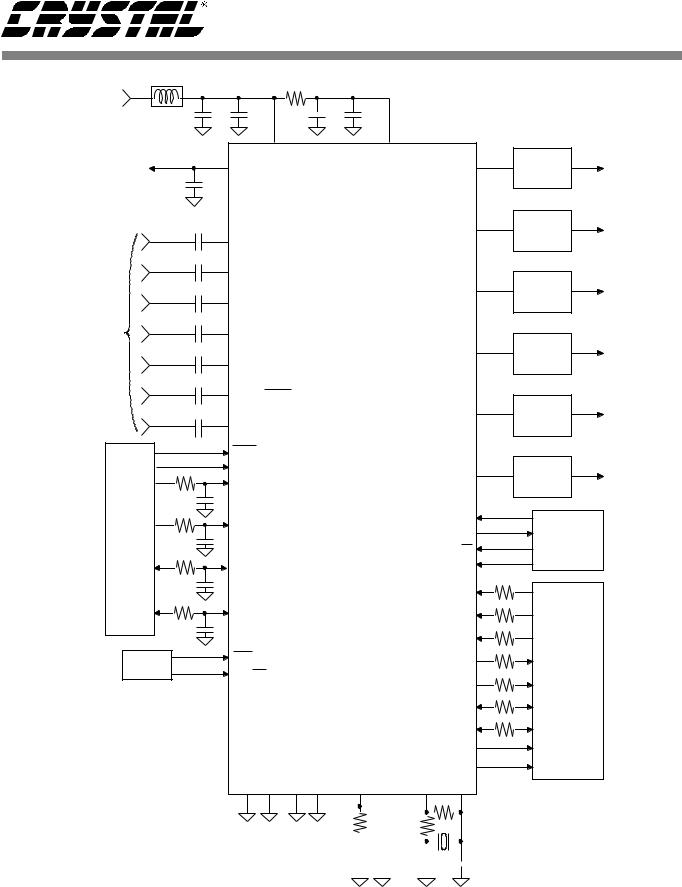
RS = 50 Ω |
|
|
|
|
|
|
|
|
|
SDOUT2 |
|
Audio |
|
|
|
|
|
|
|
|
|
37 |
RS |
||
RD = 475 Ω |
|
|
|
|
|
|
|
|
DSP |
|||
|
|
|
|
|
|
|
|
LRCK |
R |
|
||
|
|
|
|
|
|
|
|
|
|
38 |
|
|
All unused digital inputs |
|
|
|
|
|
|
|
SCLK |
S |
|
||
|
|
|
|
|
|
|
|
|
||||
should be tied to DGND. |
|
|
|
|
|
|
31 |
|
|
|||
All unused analog inputs |
|
|
|
|
|
|
|
CLKOUT |
|
|
||
|
|
|
|
|
|
|
30 |
|
|
|||
should be left floating. |
|
|
|
|
|
|
|
|
|
|||
|
|
|
|
|
|
OVL/ERR |
|
|
||||
|
|
|
|
|
|
|
|
|
|
|
||
* Optional if analog inputs |
AGND1, 2 |
DGND1, 2 |
FILT |
XTO |
XTI |
|
|
|||||
biased to within 1% of |
|
|
|
|
||||||||
|
|
|
|
|
|
|
|
RX2** 28 |
|
|
||
CMOUT |
|
|
|
18 |
20 |
41 |
39 |
17 |
29 |
|
|
|
|
|
|
|
|
|
|
|
|
|
|
|
|
|
|
|
|
|
|
|
|
|
|
† Only needed when inputs |
|
|
RFILT |
|
|
|
|
RX1** |
|
|
|
** |
|
256, |
|
|||||||
are used for S/PDIF. |
|
|
|
|
|
|
|
|
|
|
1xFs |
384, |
|
|||||||||
|
|
Loop Current |
|
|
|
|
|
|
|
|
|
|
|
|
|
|
512xFs |
|
||||
|
|
|
|
|
|
|
|
|
|
|
|
|
|
|
|
|
|
|||||
|
|
|
|
|
|
|
|
|
|
|
|
|
|
|
|
|
|
|
|
|
|
|
|
|
Normal |
High |
|
|
|
|
|
|
|
|
|
|
|
|
|
|
C1 |
40 pF |
40 pF |
|
|
|
|
|
|
|
|
|
|
C1** |
|
C2** |
||||||||||||
|
CFILT |
15 nF |
180 nF |
CFILT |
|
|
|
|
|
CRIP |
|
|
|
|
|
|
|
|
C2 |
10 pF |
40 pF |
|
|
RFILT |
43 kΩ |
3.3 kΩ |
|
|
|
|
|
|
|
|
|
|
|
|
|
|
RX1 |
300 kΩ |
short |
|
|
|
|
|
|
|
|
|
|
|
|
|
|
|
||||||||||
|
CRIP |
1.5 nF |
18 nF |
|
|
|
|
|
|
|
|
|
|
|
|
|
|
RX2 |
10 MΩ |
open |
|
|
|
Figure 1. Recommended Connection Diagram |
|
|
|
|
|||||||||||||||||
|
|
|
|
|
|
|
|
|
|
|
|
|
|
|
|
|
|
|
|
|
|
|
DS188F1 |
|
|
|
|
|
|
|
|
|
|
|
|
|
|
|
|
|
|
|
9 |
||
FUNCTIONAL DESCRIPTION
Overview
The CS4226 has 2 channels of 20-bit analog-to- digital conversion and 6 channels of 20-bit digital- to-analog conversion. A mono 20-bit ADC is also provided. All ADCs and DACs are delta-sigma converters. The stereo ADC inputs have adjustable input gain, while the DAC outputs have adjustable output attenuation. The device also contains an S/PDIF receiver capable of receiving compressed AC-3/MPEG or uncompressed digital audio data.
Digital audio data for the DACs and from the ADCs is communicated over separate serial ports. This allows concurrent writing to and reading from the device. The CS4226 functions are controlled via a serial microcontroller interface. Figure 1 shows the recommended connection diagram for the CS4226.
Analog Inputs
Line Level Inputs
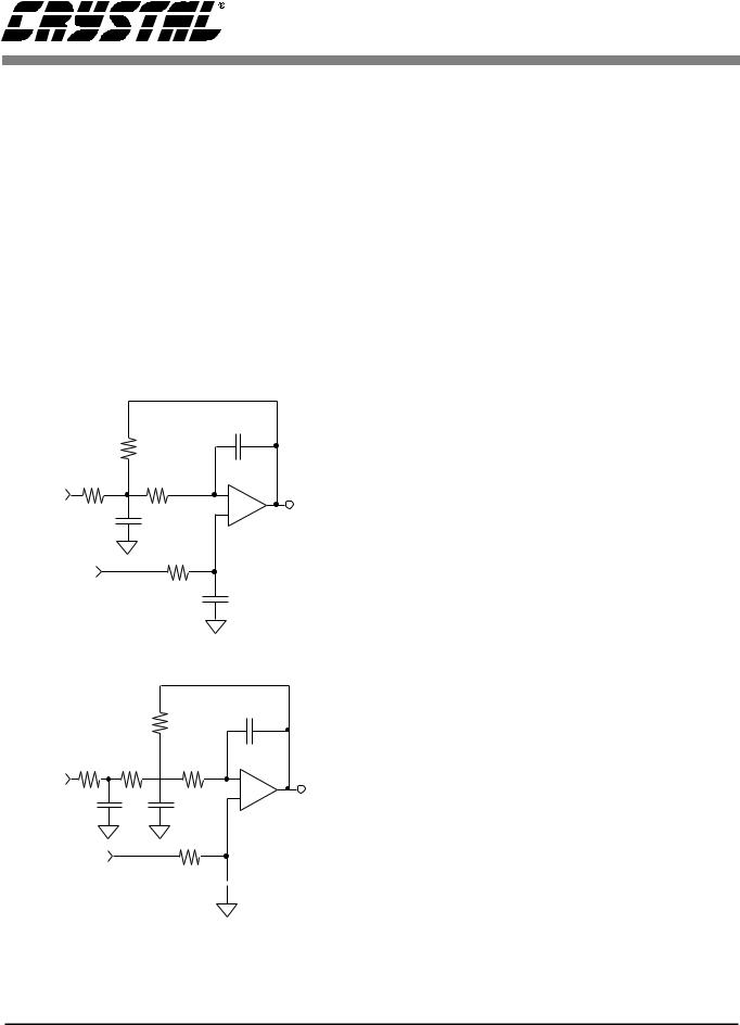
AIN1R, AIN1L, AIN2R, AIN2L, AIN3R, AIN3L and AINAUX are the line level input pins (See Figure 1). These pins are internally biased to the CMOUT voltage. A 10 μF DC blocking capacitor placed in series with the input pins allows signals centered around 0 V to be input to the CS4226. Figure 2 shows an optional dual op amp buffer which combines level shifting with a gain of 0.5 to attenuate the standard line level of 2 Vrms to 1 Vrms. The CMOUT reference level is used to bias the opamps to approximately one half the supply voltage. With this input circuit, the 10 μF DC blocking caps in Figure 1 may be omitted. Any remaining DC offset will be removed by the internal high-pass filters.
Selection of stereo the input pair (AIN1L/R, AIN2L/R or AIN3L/R) for the 20-bit ADC’s is accomplished by setting the AIS1/0 bits (ADC analog input mux control), which are accessible in the
|
|
|
CS4226 |
|
|
|
100 pF |
Line In |
3.3 μF |
20 k |
10 k |
|
|||
Right |
|
|
- |
|
|
AINxR |
|
|
|
|
|
|
|
|
+ |
Example
Op-Amps are 5 k
MC34074 or
CMOUT
MC33078
|
0.47 μF |
|
|
|
Line In |
3.3 μF |
20 k |
+ |
AINxL |
|
- |
|||
Left |
|
|
|
|
|
|
|
|
10 k |
|
|
|
|
100 pF |
Figure 2. Optional Line Input Buffer
ADC Control Byte. On-chip anti-aliasing filters follow the input mux providing anti-aliasing for all input channels.
The analog inputs may also be configured as differential inputs. This is enabled by setting bits AIS1/0=3. In the differential configuration, the left channel inputs reside on pins 10 and 11, and the right channel inputs reside on pins 12 and 13 as described in Table 1 below. In differential mode, the full scale input level is 2 Vrms.
Single-ended |
Pin # |
Differential Inputs |
AIN3L |
Pin 10 |
AINL+ |
AIN3R |
Pin 9 |
unused |
|
|
|
AIN2L |
Pin 11 |
AINL- |
AIN2R |
Pin 12 |
AINR- |
AIN1L |
Pin 14 |
unused |
AIN1R |
Pin 13 |
AINR+ |
Table 1. Single-ended vs Differential Input Pin Assignments
The analog signal is input to the mono ADC via the AINAUX pin.
Independent Muting of both the stereo ADC’s and the mono ADC is possible through the ADC Control Byte with the MUTR, MUTL and MUTM bits.
10 |
DS188F1 |
Adjustable Input Gain
The signals from the line inputs are routed to a programmable gain circuit which provides up to 9 dB of gain in 3 dB steps. The gain is adjustable through the Input Control Byte. Right and left channel gain settings are controlled independently with the GNR1/0 and GNL1/0 bits. Level changes occur immediately on register updates. To minimize audible artifacts, level changes should be done with the channel muted.
The ADC Status Report Byte provides feedback of input level for each ADC channel. This register continously monitors the ADC output and records the peak output level since the last register read. Reading this register causes it to reset to 0 and peak monitoring begins again.
High Pass Filter
The operational amplifiers in the input circuitry driving the CS4226 may generate a small DC offset into the A/D converter. The CS4226 includes a high pass filter after the decimator to remove any DC offset which could result in recording a DC level, possibly yielding "clicks" when switching between devices in a multichannel system.
The characteristics of this first-order high pass filter are outlined Table 2 below for an output sample rate of 44.1 kHz. This filter response scales linearly with sample rate.
Frequency Response |
-3dB @ 3.4 Hz |
|
-0.13 dB @ 20 Hz |
Phase Deviation |
10 degrees @ 20 Hz |
Passband Ripple |
None |
Table 2. High Pass Filter Characteristics
Analog Outputs
Line Level Outputs
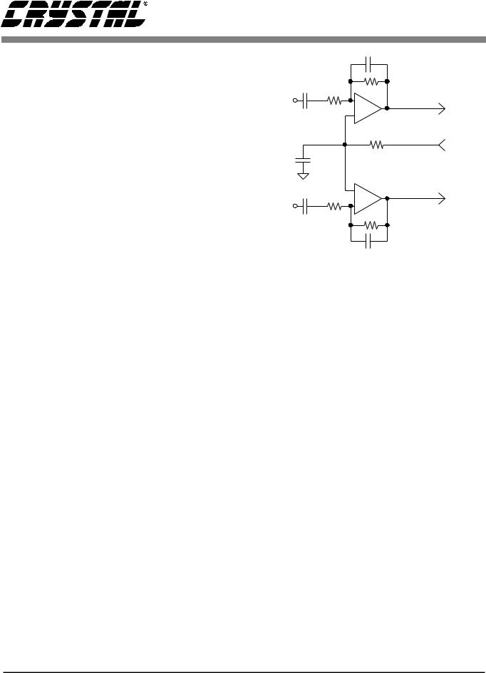
The CS4226 contains an on-chip buffer amplifier producing single-ended outputs capable of driving 10 kΩ loads. Each output (AOUT 1-6) will produce
CS4226
a nominal 2.83 Vpp (1 Vrms) output with a 2.3 volt quiescent voltage for a full scale digital input. The recommended off-chip analog filter is a 2nd order Butterworth with a -3 dB corner at Fs, see Figure 3. This filter provides out-of-band noise attenuation along with a gain of 2, providing a 2 Vrms output signal. A 3rd order Butterworth filter with a -3dB corner at 0.75 Fs can be used if greater out of band noise filtering is desired. The CS4226 DAC interpolation filter is a linear phase design which has been pre-compensated for an external 2nd order Butterworth filter to provide a flat frequency response and linear phase response over the passband. If this filter is not used, small frequency response magnitude and phase errors will occur.
Output Level Attenuator
The DAC outputs are each routed through an attenuator which is adjustable in 1 dB steps. Output attenuation is available through the Output Attenuator Data Bytes. Level changes are implemented in the analog domain such that the noise is attenuated by the same amount as the signal , until the residual output noise is equal to the noise floor in the mute state; at this point attenation is implemented in the digital domain. The change from analog to digital attenuation occurs at -23 dB. Level changes only take effect on zero crossings to minimize audible artifacts. If there is no zero crossing, then the requested level change will occur after a time-out period between 512 and 1024 frames (11.6 ms to 23.2 ms at 44.1 kHz frame rate). There is a separate zero crossing detector for each channel. Each ACC bit (Acceptance bit) in the DAC Status Report Byte gives feedback on when a volume control change has taken effect. This bit goes high when a new setting is loaded and returns low when it has taken effect. Volume control changes can be instantaneous by setting the Zero Crossing Disable (ZCD) bit in the DAC Control Byte to 1.
Each output can be independently muted via mute control bits, MUT6-1, in the DAC Control Byte.
DS188F1 |
11 |
The mute also takes effect on a zero-crossing or after a timeout. In addition, the CS4226 has an optional mute on consecutive zeros feature, where all DAC outputs will mute if they receive between 512 and 1024 consecutive zeros (or -1 code) on all six channels. A single non-zero value will unmute the DAC outputs. This feature can be disabled with the MUTC bit in the DAC Control Byte. When using the internal PLL as the clock source, all DACs will instantly mute when the PLL detects an error.
Clock Generation
The master clock to operate the CS4226 may be generated by using the on-chip inverter and an ex-
|
|
150pF |
|
22 kΩ |
|
11 kΩ |
3.9 kΩ |
_ |
AOUT |
|
|
|
|
|
|
1000pF |
+ |
|
Example |
|
|
|
|
|
5 kΩ |
Op-Amps |
|
are |
|
CMOUT |
|
MC33078 |
|
|
0.47 μF |
2-Pole Butterworth Filter
560 pF
|
5.85 kΩ |
|
1.1 kΩ 4.75 kΩ |
1.21 kΩ |
_ |
AOUT |
|
|
|
|
|
5600 pF |
5600 pF |
+ |
|
5 kΩ
CMOUT
 0.47 μF
3-Pole Butterworth Filter
Figure 3.
CS4226
ternal crystal, by using the on-chip PLL, or by using an external clock source. In all modes it is required to have SCLK and LRCK synchronous to the selected master clock.
Clock Source
The CS4226 requires a high frequency master clock to run the internal logic. The Clock Source bits, CS0/1/2 in Clock Mode Byte, determine the source of the clock. A high frequency crystal can be connected to XTI and XTO, or a high frequency clock can be applied to XTI. In both these cases, the internal PLL is disabled, and the VCO turns off. The externally supplied high frequency clock can be 256 Fs, 384 Fs or 512 Fs; this is set by the CI0/1 bits in the Clock Mode Byte. When using the onchip crystal oscillator, external loading capacitors are required, see Figure 1. High frequency crystals (>8MHz) should be parallel resonant, fundamental mode and designed for 20 pF loading (equivalent to 40 pF to ground on each leg).
Alternatively, the on-chip PLL may be used to generate the required high frequency clock. The PLL input clock is 1 Fs, and may be input from LRCKAUX, LRCK, or from XTI/XTO. In this last case, a 1 Fs clock may be input into XTI, or a 1 Fs crystal attached across XTI/XTO. When an external 1 Fs crystal is attached, extra components will be required, see Figure 1. The PLL will lock onto a new 1 Fs clock in about 90 ms. If the PLL input clock is removed, the VCO will drift to the low frequency end of its frequency range.
The PLL can also be used to lock to an S/PDIF data source on RX1, RX2, RX3, or RX4. Source selection is accomplished with the CS2/1/0 bits in the Clock Mode Byte. The PLL will lock to an S/PDIF source in about 90 ms.
Finally, the PLL has two filter loop current modes, normal and high current, that are selected via the LC bit in the Converter Control Byte. In the normal mode, the loop current is 25 μA. In the high current
12 |
DS188F1 |

mode, the loop current is 300 μA. The high current mode allows the use of lower impedance filter components which minimizes the influences of board contamination. See the table in Figure 1 for filter component values in each mode.
Master Clock Output
CLKOUT is a master clock output provided to allow synchronization of external components. Available CLKOUT frequencies of 1 Fs, 256 Fs, 384 Fs, and 512 Fs, are selectable by the CO0/1 bits of the Clock Mode Byte.
Generation of CLKOUT for 384 Fs and 512 Fs is accomplished with an on chip clock multiplier and may contain clock jitter. The source of the 256 Fs CLKOUT is the output of the PLL or a divided down clock from the XTI/XTO input. If 384 Fs is chosen as the input clock at XTI and 256 Fs is chosen as the output, CLKOUT will have approximately a 33% duty cycle. In all other cases CLKOUT will typically have a 50% duty cycle.
Synchronization
The DSP port and Auxiliary port must operate synchronously to the CS4226 clock source. The serial port will force a reset of the data paths in an attempt to resynchronize if non-synchronous data is input to the CS4226. It is advisable to mute the DACs when changing from one clock source to another to avoid the output of undesirable audio signals as the CS4226 resynchronizes.
Digital Interfaces
There are 3 digital audio interface ports: the audio DSP port, the auxiliary digital audio port, and the S/PDIF reciever. The serial data is represented in 2’s complement format with the MSB-first in all formats.
Audio DSP Serial Interface Signals
The serial interface clock, SCLK, is used for transmitting and receiving audio data. The active edge
CS4226
of SCLK is chosen by setting the DSCK bit in the DSP Port Mode Byte. SCLK can be generated by the CS4226 (master mode) or it can be input from an external SCLK source (slave mode). Mode selection is set with the DMS1/0 bits in the DSP Port Mode Byte. The number of SCLK cycles in one system sample period is programmable to be 32, 48, 64, or 128 by setting the DCK1/0 bits in the DSP Port Mode Byte.
The Left/Right clock (LRCK) is used to indicate left and right data and the start of a new sample period. It may be output from the CS4226, or it may be generated from an external controller. The frequency of LRCK must be equal to the system sample rate, Fs.
SDIN1, SDIN2, and SDIN3 are the data input pins, each of which drive a pair of DACs. SDOUT1 and SDOUT2 can carry the output data from the two 20-bit ADC’s, the mono ADC, the auxiliary digital audio port, and the S/PDIF receiver. Selection depends on the IS1/0 bits in the ADC control byte. The audio DSP port may also be configured so that all 6 DAC’s data is input on SDIN1, and all 3 ADC’s data is output on SDOUT1. Table 3 outlines the serial interface ports.
DAC Inputs
SDIN1 |
left channel |
DAC #1 |
|
right channel |
DAC #2 |
|
single line |
All 6 DAC channels |
SDIN2 |
left channel |
DAC #3 |
|
right channel |
DAC #4 |
SDIN3 |
left channel |
DAC #5 |
|
right channel |
DAC #6 |
Table 3. DSP Serial Interface Ports
Audio DSP Serial Interface Formats
The audio DSP port supports 7 alternate formats, shown in Figures 4, 5, and 6. These formats are chosen through the DSP Port Mode Byte with the DDF2/1/0 bits.
Formats 5 and 6 are single line data modes where all DAC channels are combined onto a single input
DS188F1 |
13 |

CS4226
FORMAT 0, 1, 2: |
LRCK |
|
Left |
|
Right |
|
Format 0: M = 20 |
SCLK |
|
|
|
|
|
Format 1: M = 18 |
|
|
|
|
|
|
|
|
|
|
|
|
|
Format 2: M = 16 |
SDIN |
LSB |
MSB |
LSB |
MSB |
LSB |
|
|
|
M SCLKs |
|
M SCLKs |
|
FORMAT 3: |
LRCK |
|
Left |
|
Right |
|
|
SCLK |
|
|
|
|
|
|
SDIN |
MSB |
LSB |
MSB |
LSB |
MSB |
FORMAT 4: |
LRCK |
|
Left |
|
Right |
|
|
SCLK |
|
|
|
|
|
|
SDIN |
MSB |
LSB |
MSB |
LSB |
|
Note: SCLK shown for DSCK = 0. SCLK inverted for DSCK = 1.
Figure 4. Audio DSP and Auxiliary Port Data Input Formats
FORMAT 0, 1, 2: |
LRCK |
|
Left |
|
Right |
|
Format 0: M = 20 |
SCLK |
|
|
|
|
|
Format 1: M = 18 |
|
|
|
|
|
|
|
|
|
|
|
|
|
Format 2: M = 16 |
SDOUT |
LSB |
MSB |
LSB |
MSB |
LSB |
|
|
|
M SCLKs |
|
M SCLKs |
|
FORMAT 3: |
LRCK |
|
Left |
|
Right |
|
|
SCLK |
|
|
|
|
|
|
SDOUT |
MSB |
LSB |
MSB |
LSB |
MSB |
FORMAT 4: |
LRCK |
|
Left |
|
Right |
|
|
SCLK |
|
|
|
|
|
|
SDOUT |
MSB |
LSB |
MSB |
LSB |
|
Note: SCLK shown for DSCK = 0. SCLK inverted for DSCK = 1.
Figure 5. Audio DSP Port Data Output Formats
64 SCLKS 64 SCLKS
FORMAT 5: LRCK
|
SCLK |
|
|
|
|
|
|
|
|
|
|
|
|
|
|
|
SDIN1 |
MSB |
LSB MSB |
LSB MSB |
LSB |
MSB |
LSB MSB |
LSB MSB |
LSB |
MSB |
|||||
|
|
DAC #1 |
DAC #3 |
DAC #5 |
|
DAC #2 |
DAC #4 |
DAC #6 |
|
||||||
|
|
|
20 clks |
|
20 clks |
20 clks |
|
|
20 clks |
|
20 clks |
20 clks |
|
|
|
|
SDOUT1 |
SDOUT1 |
SDOUT2 |
|
|
|
SDOUT1 |
SDOUT2 |
|
|
|
||||
|
|
|
20 clks |
|
20 clks |
|
|
|
20 clks |
|
20 clks |
|
|
|
|
|
|
|
|
|
128 SCLKS |
|
|
|
|
|
128 SCLKS |
|
|
|
|
FORMAT 6: LRCK (out) |
|
|
|
|
|
|
|
|
|
|
|
|
|
|
|
(MASTER SCLK (out) |
|
|
|
|
|
|
|
|
|
|
|
|
|
|
|
MODE |
SDIN1 |
|
MSB |
LSB |
MSB |
LSB |
|
MSB |
LSB |
|
MSB |
LSB |
MSB |
LSB |
MSB LSB |
ONLY) |
|
|
|
||||||||||||
|
|
|
|
|
|
|
|
|
|
|
|
|
|
|
|
|
|
|
DAC #1 |
|
DAC #3 |
|
DAC #5 |
|
DAC #2 |
|
DAC #4 |
DAC #6 |
|||
|
|
|
32 clks |
|
32 clks |
|
|
32 clks |
|
|
32 clks |
|
32 clks |
|
32 clks |
|
SDOUT1 |
|
SDOUT1 |
|
SDOUT2 |
|
|
|
|
SDOUT1 |
|
SDOUT2 |
|
||
|
|
|
32 clks |
|
32 clks |
|
|
|
|
32 clks |
|
32 clks |
|
||
|
|
|
|
|
Figure 6. One data line modes |
|
|
|
|
||||||
14 |
|
|
|
|
|
|
|
|
|
|
|
|
|
|
DS188F1 |

and all ADC channels are combined onto a single output. Format 6 is available in Master Mode only. See figure 6 for details.
Auxiliary Audio Port Signals
The auxiliary port provides an alternate way to input digital audio signals into the CS4226, and allows the CS4226 to synchronize the system to an external digital audio source. This port consists of serial clock, data and left/right clock pins named, SCLKAUX, DATAUX and LRCKAUX. The Auxiliary Audio Port input is output on SDOUT1 when the IS bits are set to 1 or 2 in the ADC Control Byte. Additionally, setting IS to 2 routes the stereo ADC outputs to SDOUT2. There is approximately a two frame delay from DATAUX to SDOUT1. When the auxiliary port is used, the frequency of LRCKAUX must equal to the system sample rate, Fs, but no particular phase relationship is required.
De-emphasis and muting on error conditions can be performed on input data to the auxiliary audio port; this is controlled by the Auxiliary Port Control Byte.
Auxiliary Audio Port Formats
Data input on DATAUX is clocked into the part by SCLKAUX using the format selected in the Auxiliary Port Mode Byte. The auxiliary audio port supports the same 5 formats as the audio DSP port in multi-data line mode. LRCKAUX is used to indicate left and right data samples, and the start of a new sample period. SCLKAUX and LRCKAUX may be output from the CS4226, or they may be generated from an external source, as set by the AMS1/0 control bits in the Auxiliary Port Mode Byte.
S/PDIF Receiver
The CS4226 reconfigures its auxiliary digital audio port as an S/PDIF receiver if CS2/1/0 in the Clock Mode Byte are set to be 4, 5, 6, or 7. In this mode
CS4226
RX1, RX2, RX3, or RX4 can be chosen as the S/PDIF input source.
The PLL will lock to the requested data source and setting IS1/0 = 1 or 2 in the ADC Control Byte routes the recovered output to SDOUT1 (channel A to left, channel B to right). All 24 received data bits will pass through the part to SDOUT1 except when the serial port is configured with 32 SCLK’s per frame or in Format 5. For these cases, the 16 or 20 MSB’s respectively will be output.
The error flags are reported in the Receiver Status Byte. The LOCK bit indicates whether the PLL is locked to the incoming S/PDIF data. Parity, Biphase, or Validity errors (PAR=1, BIP=1 or V=1) will cause the last valid data sample to be held at the receiver input until the error condition no longer is present (see Hold section). Mute on extended hold can also be enabled through the Auxiliary Port Control Byte (see Hold section).
Other error flags include confidence, CONF, and cyclic redundancy check, CRC. The CONF flag occurs when the received data eye opening is less than half a bit period. This indicates that the quality of the transmission link is poor and does not meet the digital audio interface standards. The CRC flag is updated at the beginning of a channel status block and is only valid when the professional format of channel status data is received. This error indicates when the CS4226 calculated CRC value does not match the CRC byte of the received channel status block.
The OVL/ERR pin will go high to flag an error. It is a latched logical OR of the Parity, Biphase, Validity, and Lock error flags in the Receiver Status Byte which is reset at the end of each frame. However, Parity, Biphase, or Validity errors can be masked from the pin by clearing the PM, BM, and VM bits respectively, of the Input Control Byte.
The first four bytes of the Channel Status block for both channel A and B can be accessed in the Receiver Channel Status Bytes. When the CV bit is
DS188F1 |
15 |

high, these bytes are being updated and may be invalid. Additionally, the audio/non-audio, AC- 3/MPEG data stream indicator and sampling frequency channel status bits may be output to pins 9, 10, 11 and 12, respectively, see Table 4. This is accomplished by setting the CSP bit to 1 in the Auxiliary Status Output Byte. The FREQ0/1 channel status bit outputs are decoded from the sampling frequency channel status bits after first referencing channel status byte 0, bit 0 (PRO or consumer bit) which indicates the appropriate location of these bits in the channel status data stream.
The received user bit is output on the HOLD/RUBIT pin if the HPC bit in the AUX Port Control Byte is set to 1. It can be sampled with the rising or falling edge of LRCK if the audio DSP port is in Master Mode.
AUDIO |
Pin 9 |
0 |
- Audio data |
|
|
|
1 |
- Non-audio data |
|
AUTODATA |
Pin 10 |
0 - No preamble detected in |
||
|
|
last 4096 frames |
||
|
|
1 |
- Preamble detected |
|
FREQ0/1 |
Pin 11/12 |
00 |
- 44.1 kHz |
|
|
|
01 |
- 48 kHz |
|
|
|
10 |
- Reserved |
|
|
|
11 - 32 kHz |
||
Table 4. S/PDIF Receiver Status Outputs
AC-3/MPEG Auto Detection
For AC-3/MPEG applications, it is important to know whether the incoming S/PDIF data stream is digital audio or compressed AC-3/MPEG data. This information is typically conveyed by setting channel status bit 1 (audio/non-audio bit), but some AC-3/MPEG sources may not strictly adhere to this convention and the bit may not be properly set. The CS4226 S/PDIF receiver has the capability to automatically detect whether the incoming data is a compressed AC-3/MPEG input. This is accomplished by looking for an AC-3/MPEG 96-bit sync code consisting of six 16-bit words. The 96-bit sync code consists of: 0x0000, 0x0000, 0x0000, 0x0000, 0xF872, and 0x4E1F. When the sync code
CS4226
is detected, the AUTODATA indicator (pin 10) will go high. If no additional sync codes are detected within the next 4096 frames, the AUTODATA indicator pin will return low until another sync code is detected.
Control Port Signals
The control port is used to load all the internal settings. The operation of the control port may be completely asynchronous with the audio sample rate. However, to avoid potential interference problems, the control port pins should remain static if no operation is required.
The control port has 2 modes: SPI and I2C, with the CS4226 as a slave device. The SPI mode is selected by setting the I2C/SPI pin low, and I2C is selected by setting the I2C/SPI pin high. The state of this pin is continuously monitored.
SPI Mode
In SPI mode, CS is the CS4226 chip select signal, CCLK is the control port bit clock, (input into the CS4226 from the microcontroller), CDIN is the input data line from the microcontroller, CDOUT is the output data line to the microcontroller, and the chip address is 0010000. Data is clocked in on the rising edge of CCLK and out on the falling edge.
Figure 7 shows the control port timing in SPI mode. To write to a register, bring CS low. The first 7 bits on CDIN form the chip address, and they must be 0010000. The eighth bit is a read/write indicator (R/W), which should be low to write. The next 8 bits form the Memory Address Pointer (MAP), which is set to the address of the register that is to be updated. The next 8 bits are the data which will be placed into register designated by the MAP. During writes, the CDOUT output stays in the high impedance state. It may be externally pulled high or low with a 47 kΩ resistor.
The CS4226 has a MAP auto increment capability, enabled by the INCR bit in the MAP register. If INCR is a zero, then the MAP will stay constant for
16 |
DS188F1 |
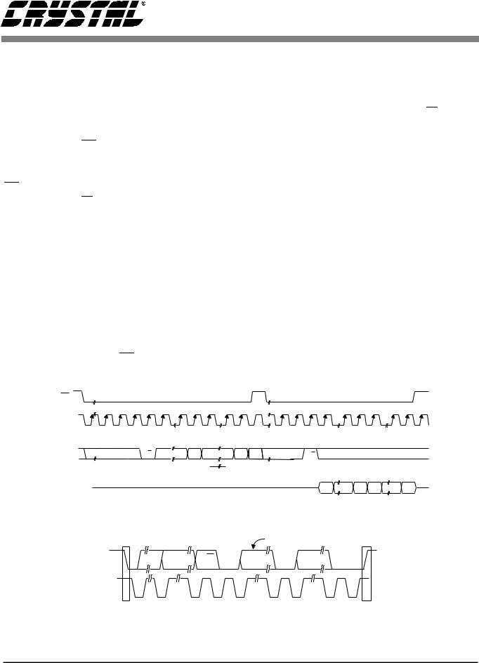
successive reads or writes. If INCR is set to a 1, then MAP will auto increment after each byte is read or written, allowing block reads or writes of successive registers.
To read a register, the MAP has to be set to the correct address by executing a partial write cycle which finishes (CS high) immediately after the MAP byte. The auto MAP increment bit (INCR) may be set or not, as desired. To begin a read, bring CS low, send out the chip address and set the read/write bit (R/W) high. The next falling edge of CCLK will clock out the MSB of the addressed register (CDOUT will leave the high impedance state). If the MAP auto increment bit is set to 1, the data for successive registers will appear consecutively.
CS4226
the 7 bit address field must be 00100. To communicate with a CS4226, the LSBs of the chip address field, which is the first byte sent to the CS4226, should match the settings of the AD1, AD0 pins. The eighth bit of the address bit is the R/W bit (high for a read, low for a write). The next byte is the Memory Address Pointer (MAP) which selects the register to be read or written. If the operation is a write, the next byte is the data to be written to the register pointed to by the MAP. If the operation is a read, the contents of the register pointed to by the MAP will be output. Setting the auto increment bit in MAP, allows successive reads or writes of consecutive registers. Each byte is separated by an acknowledge bit. I2C bus is a registered trademark of Philips Semiconductors.
I2C Mode
In I2C mode, SDA is a bidirectional data line. Data is clocked into and out of the part by the clock, SCL, with the clock to data relationship as shown in Figure 8. There is no CS pin. Pins AD0, AD1 form the partial chip address. The upper 5 bits of
Control Port Bit Definitions
All registers can be written and read back, except the DAC Status Report Byte, ADC Status Report Byte, Receiver Status Byte, and the Receiver Channel Status Bytes, which are read only. See the bit definition tables for bit assignment information.
CS |
|
|
|
|
|
|
|
|
|
|
CCLK |
|
|
|
|
|
|
|
|
|
|
|
CHIP |
|
MAP |
DATA |
|
CHIP |
|
|
|
|
|
ADDRESS |
|
ADDRESS |
|
|
|||||
CDIN |
0010000 |
R/W |
|
MSB |
LSB |
0010000 |
R/W |
|
|
|
|
|
|
|
byte 1 |
byte n |
|
|
|
|
|
CDOUT |
|
|
|
|
|
|
|
MSB |
LSB MSB |
LSB |
|
|
|
|
|
|
High Impedance |
|
|
||
|
MAP = Memory Address Pointer |
|
|
|
|
|
|
|||
|
|
|
Figure 7. Control Port Timing, SPI mode |
|
|
|||||
|
|
|
|
|
|
|
Note 1 |
|
|
|
|
SDA |
00100 |
ADDR |
R/W |
ACK |
DATA |
ACK |
DATA |
ACK |
|
|
AD1-0 |
1-8 |
1-8 |
|
||||||
|
SCL |
|
|
|
|
|
|
|
|
|
|
Start |
|
|
|
|
|
|
|
Stop |
|
Note 1: If operation is a write, this byte contains the Memory Address Pointer, MAP.
Figure 8. Control Port Timing, I2C Mode
DS188F1 |
17 |

Power-up/Reset/Power Down Mode
Upon power up, the user should hold PDN=0 until the system’s power supply has stabilized. In this state, the control port is reset to its default settings. When PDN goes high, the device remains in a low power mode in which the control port is active, but CMOUT will not supply current. The desired settings should be loaded in while keeping the RS bit set to 1. Normal operation is achieved by setting the RS bit to zero in the Converter Control Byte. Once set to 0, the part powers up and an offset calibration occurs. This process lasts approximately 50 ms.
Reset/power down is achieved by lowering the PDN pin causing the part to enter power down. Once PDN goes high, the control port is functional and the desired settings should be loaded in while keeping the RS bit set to 1. The remainder of the chip remains in a low power reset state until the RS bit in the Converter Control Byte is set to 0.
The CS4226 will also enter a stand-by mode if the master clock source stops for approximately 10 μs or if the LRCK is not synchronous to the master clock. The control port will retain its current settings when in stand-by mode.
DAC Calibration
Output offset voltage is minimized by an internal calibration cycle. A calibration will automatically occur anytime the part comes out of reset, including the power-up reset, when the master clock source to the part changes by changing the CS or CI bits in the Clock Mode Byte or when the PLL goes out of lock and then re-locks.
The CS4226 can be re-calibrated whenever desired. A control bit, CAL, in the Converter Control Byte, is provided to initiate a calibration. The sequence is:
1)Set CAL to 1, the CS4226 sets CALP to 1 and begins to calibrate.
2)CALP will go to 0 when the calibration is completed.
CS4226
Additional calibrations can be implemented by setting CAL to 0 and then to 1.
De-Emphasis
The S/PDIF receiver can be enabled to process 24 bits of received data (20 bits of audio data and four auxiliary bits) or process 20 bits of audio data (no auxiliary bits). Setting DEM24=0 in the Auxiliary Port Control Byte, will enable all 24 received data bits to be processed with de-emphasis when de-em- phasis is enabled. When setting DEM24=1, the four auxiliary bits in the receiver data stream will pass through unchanged and only the 20 audio data bits will be processed.
The CS4226 is capable of digital de-emphasis for 32, 44.1, or 48 kHz sample rates. Implementation of digital de-emphasis requires reconfiguration of the digital filter to maintain the filter response shown in Figure 9 at multiple sample rates. The Auxiliary Port Control Byte selects the de-empha- sis control method. De-emphasis may be enabled under hardware control, using the DEM pin (DEM2/1/0=4,5,6), by software control using the DEM bit (DEM2/1/0=0,1,2,3), or by the emphasis bits in the channel status data when the S/PDIF receiver is chosen as the clock source (DEM2/0/1=7). If no frequency information is present, the filter defaults to 44.1 kHz.
Gain |
|
|
dB |
|
|
T1=50 μs |
|
|
0dB |
|
|
|
|
T2 = 15 μs |
-10dB |
|
|
F1 |
F2 |
Frequency |
Figure 9. De-emphasis Curve
18 |
DS188F1 |
 Loading...