


 Loading...
CS43L22
Low Power, Stereo DAC w/Headphone & Speaker Amps
FEATURES
98 dB Dynamic Range (A-wtd)
88 dB THD+N
Headphone Amplifier - GND Centered
–No DC-Blocking Capacitors Required
–Integrated Negative Voltage Regulator
–2 x 23 mW into Stereo 16 Ω @ 1.8 V
–2 x 44 mW into Stereo 16 Ω @ 2.5V
Stereo Analog Input Passthrough Architecture
–Analog Input Mixing
–Analog Passthrough with Volume Control
Digital Signal Processing Engine
–Bass & Treble Tone Control, De-Emphasis
–PCM Input w/Independent Vol Control
–Master Digital Volume Control and Limiter
–Soft-Ramp & Zero-Cross Transitions
Programmable Peak-Detect and Limiter
Beep Generator w/Full Tone Control
–Tone Selections Across Two Octaves
–Separate Volume Control
–Programmable On and Off Time Intervals
–Continuous, Periodic, One-Shot Beep Selections
Class D Stereo/Mono Speaker Amplifier
No External Filter Required
High Stereo Output Power at 10% THD+N
–2 x 1.00 W into 8 Ω @ 5.0 V
–2 x 550 mW into 8 Ω @ 3.7 V
–2 x 230 mW into 8 Ω @ 2.5 V
High Mono Output Power at 10% THD+N
–1 x 1.90 W into 4 Ω @ 5.0 V
–1 x 1.00 W into 4 Ω @ 3.7 V
–1 x 350 mW into 4 Ω @ 2.5 V
Direct Battery Powered Operation
–Battery Level Monitoring & Compensation
81% Efficiency at 800 mW
Phase-Aligned PWM Output Reduces Idle Channel Current
Spread Spectrum Modulation
Low Quiescent Current
Serial
Audio
Input
Reset
I²C
Control
+1.65 V to +3.47 V
Interface Supply
Shifter |
Serial Audio Port |
Level |
|
|
Control Port |
+1.60 V to +5.25 V
Battery
Battery Level Monitoring & Compensation
|
Pulse-Width |
|
|
|
Modulator |
|
|
Digital Volume, |
|
|
|
Mono Mix, |
Multi-bit |
|
|
Limiter, Bass, |
ΔΣ DAC |
|
|
Treble Adjust |
|
|
|
Beep |
|
|
|
Generator |
Summing |
|
|
Σ |
Σ |
||
Amplifiers |
|||
|
+1.65 V to +2.63 V |
1 2 3 4 |
1 2 3 4 |
|
Digital Supply |
|||
Left |
Right |
||
|
Inputs |
Inputs |
|
+ Stereo/Mono |
|
|
- |
Full-Bridge |
|
+- |
Speaker |
|
|
Outputs |
Class D Amps |
|
|
|
|
Left HP/Line |
|
|
Output |
|
|
Right HP/Line |
|
|
Output |
Ground-Centered |
|
|
Amps |
|
Speaker/HP |
|
|
|
-VHP |
+VHP |
Switch |
|
||
Charge Pump +1.65 V to +2.63 V
Headphone Supply
+1.65 V to +2.63 V
Analog Supply
|
Copyright Cirrus Logic, Inc. 2010 |
MARCH '10 |
http://www.cirrus.com |
(All Rights Reserved) |
DS792F2 |

CS43L22
System Features
12, 24, and 27 MHz Master Clock Support in Addition to Typical Audio Clock Rates
High Performance 24-bit Converters
–Multi-bit Delta–Sigma Architecture
General Description
The CS43L22 is a highly integrated, low power stereo DAC with headphone and Class D speaker amplifiers. The CS43L22 offers many features suitable for low power, portable system applications.
–Very Low 64Fs Oversampling Clock Reduces The DAC output path includes a digital signal processing en-
Power Consumption
Low Power Operation
–Stereo Analog Passthrough: 10 mW @ 1.8 V
–Stereo Playback: 14 mW @ 1.8 V
Variable Power Supplies
–1.8 V to 2.5 V Digital & Analog
–1.6 V to 5 V Class D Amplifier
–1.8 V to 2.5 V Headphone Amplifier
–1.8 V to 3.3 V Interface Logic
Power Down Management
–DAC, Passthrough Amplifier, Headphone Amplifier, Speaker Amplifier
Flexible Clocking Options
–Master or Slave Operation
–Quarter-Speed Mode - (i.e. allows 8 kHz Fs while maintaining a flat noise floor up to 16 kHz)
–4 kHz to 96 kHz Sample Rates
I²CTM Control Port Operation
Headphone/Speaker Detection Input
Pop and Click Suppression
Pin-Compatible w/CS42L52
Applications
PDA’s
Personal Media Players
Portable Game Consoles
gine with various fixed function controls. Tone Control provides bass and treble adjustment of four selectable corner frequencies. Digital Volume controls may be configured to change on soft ramp transitions while the analog controls can be configured to occur on every zero crossing. The DAC also includes de-emphasis, limiting functions and a BEEP generator delivering tones selectable across a range of two full octaves.
The stereo headphone amplifier is powered from a separate positive supply and the integrated charge pump provides a negative supply. This allows a ground-centered analog output with a wide signal swing and eliminates the need for external DC-blocking capacitors.
The Class D stereo speaker amplifier does not require an external filter and provides the high efficiency amplification required by power sensitive portable applications. The speaker amplifier may be powered directly from a battery while the internal DC supply monitoring and compensation provides a constant gain level as the battery’s voltage decays.
The CS43L22 accommodates analog routing of the analog input signal directly to the headphone amplifier. This feature is useful in applications that utilize an FM tuner where audio recovered over-the-air must be transmitted to the headphone amplifier directly.
In addition to its many features, the CS43L22 operates from a low voltage analog and digital core making it ideal for portable systems that require extremely low power consumption in a minimal amount of space.
The CS43L22 is available in a 40-pin QFN package in Commercial (-40 to +85 °C) grade. The CS43L22 Customer Demonstration board is also available for device evaluation and implementation suggestions. Please refer to “Ordering Information” on page 66 for complete ordering information.
2 |
DS792F2 |

|
|
CS43L22 |
TABLE OF CONTENTS |
|
|
1. PIN DESCRIPTIONS .............................................................................................................................. |
7 |
|
1.1 |
I/O Pin Characteristics ..................................................................................................................... |
8 |
2. TYPICAL CONNECTION DIAGRAM ..................................................................................................... |
9 |
|
3. CHARACTERISTIC AND SPECIFICATIONS ...................................................................................... |
10 |
|
RECOMMENDED OPERATING CONDITIONS .................................................................................. |
10 |
|
ABSOLUTE MAXIMUM RATINGS ...................................................................................................... |
10 |
|
ANALOG OUTPUT CHARACTERISTICS .......................................................................................... |
11 |
|
ANALOG PASSTHROUGH CHARACTERISTICS .............................................................................. |
12 |
|
PWM OUTPUT CHARACTERISTICS ................................................................................................. |
13 |
|
HEADPHONE OUTPUT POWER CHARACTERISTICS ..................................................................... |
14 |
|
LINE OUTPUT VOLTAGE LEVEL CHARACTERISTICS .................................................................... |
15 |
|
COMBINED DAC INTERPOLATION & ON-CHIP ANALOG FILTER RESPONSE ............................. |
15 |
|
SWITCHING SPECIFICATIONS - SERIAL PORT .............................................................................. |
16 |
|
SWITCHING SPECIFICATIONS - I²C CONTROL PORT .................................................................... |
17 |
|
DC ELECTRICAL CHARACTERISTICS .............................................................................................. |
18 |
|
DIGITAL INTERFACE SPECIFICATIONS & CHARACTERISTICS .................................................... |
18 |
|
POWER CONSUMPTION ................................................................................................................... |
19 |
|
4. APPLICATIONS ................................................................................................................................... |
20 |
|
4.1 |
Overview ........................................................................................................................................ |
20 |
|
4.1.1 Basic Architecture ................................................................................................................. |
20 |
|
4.1.2 Line Inputs ............................................................................................................................. |
20 |
|
4.1.3 Line & Headphone Outputs ................................................................................................... |
20 |
|
4.1.4 Speaker Driver Outputs ......................................................................................................... |
20 |
|
4.1.5 Fixed Function DSP Engine .................................................................................................. |
20 |
|
4.1.6 Beep Generator ..................................................................................................................... |
20 |
|
4.1.7 Power Management .............................................................................................................. |
20 |
4.2 |
DSP Engine .................................................................................................................................. |
21 |
|
4.2.1 Beep Generator ..................................................................................................................... |
22 |
|
4.2.2 Limiter .................................................................................................................................... |
22 |
4.3 |
Analog Passthrough ....................................................................................................................... |
24 |
4.4 |
Analog Outputs .............................................................................................................................. |
25 |
4.5 |
PWM Outputs ................................................................................................................................. |
26 |
|
4.5.1 Mono Speaker Output Configuration ..................................................................................... |
27 |
|
4.5.2 VP Battery Compensation ..................................................................................................... |
27 |
|
4.5.2.1 Maintaining a Desired Output Level ........................................................................... |
27 |
4.6 |
Serial Port Clocking ....................................................................................................................... |
29 |
4.7 |
Digital Interface Formats ................................................................................................................ |
30 |
|
4.7.1 DSP Mode ............................................................................................................................. |
31 |
4.8 |
Initialization .................................................................................................................................... |
31 |
4.9 Recommended Power-Up Sequence ............................................................................................ |
31 |
|
4.10 Recommended Power-Down Sequence ...................................................................................... |
31 |
|
4.11 Required Initialization Settings ..................................................................................................... |
32 |
|
5. CONTROL PORT OPERATION ........................................................................................................... |
33 |
|
5.1 |
I²C Control ...................................................................................................................................... |
33 |
|
5.1.1 Memory Address Pointer (MAP) ............................................................................................ |
34 |
|
5.1.1.1 Map Increment (INCR) ............................................................................................... |
34 |
6. REGISTER QUICK REFERENCE ........................................................................................................ |
35 |
|
7. REGISTER DESCRIPTION .................................................................................................................. |
37 |
|
7.1 |
Chip I.D. and Revision Register (Address 01h) (Read Only) ......................................................... |
37 |
|
7.1.1 Chip I.D. (Read Only) ............................................................................................................ |
37 |
|
7.1.2 Chip Revision (Read Only) .................................................................................................... |
37 |
7.2 |
Power Control 1 (Address 02h) ...................................................................................................... |
37 |
DS792F2 |
|
3 |

|
|
CS43L22 |
|
|
|
|
|
|
7.2.1 Power Down .......................................................................................................................... |
37 |
|
|
7.3 Power Control 2 (Address 04h) ...................................................................................................... |
38 |
|
|
7.3.1 Headphone Power Control .................................................................................................... |
38 |
|
|
7.3.2 Speaker Power Control ......................................................................................................... |
38 |
|
|
7.4 Clocking Control (Address 05h) ..................................................................................................... |
38 |
|
|
7.4.1 Auto-Detect ........................................................................................................................... |
38 |
|
|
7.4.2 Speed Mode .......................................................................................................................... |
39 |
|
|
7.4.3 32kHz Sample Rate Group ................................................................................................... |
39 |
|
|
7.4.4 27 MHz Video Clock .............................................................................................................. |
39 |
|
|
7.4.5 Internal MCLK/LRCK Ratio ................................................................................................... |
39 |
|
|
7.4.6 MCLK Divide By 2 ................................................................................................................. |
40 |
|
|
7.5 Interface Control 1 (Address 06h) .................................................................................................. |
40 |
|
|
7.5.1 Master/Slave Mode ............................................................................................................... |
40 |
|
|
7.5.2 SCLK Polarity ........................................................................................................................ |
40 |
|
|
7.5.3 DSP Mode ............................................................................................................................. |
40 |
|
|
7.5.4 DAC Interface Format ........................................................................................................... |
40 |
|
|
7.5.5 Audio Word Length ................................................................................................................ |
41 |
|
|
7.6 Interface Control 2 (Address 07h) .................................................................................................. |
41 |
|
|
7.6.1 SCLK equals MCLK .............................................................................................................. |
41 |
|
|
7.6.2 Speaker/Headphone Switch Invert ........................................................................................ |
41 |
|
|
7.7 Passthrough x Select: PassA (Address 08h), PassB (Address 09h) ............................................. |
42 |
|
|
7.7.1 Passthrough Input Channel Mapping .................................................................................... |
42 |
|
|
7.8 Analog ZC and SR Settings (Address 0Ah) ................................................................................... |
42 |
|
|
7.8.1 Ch. x Analog Soft Ramp ........................................................................................................ |
42 |
|
|
7.8.2 Ch. x Analog Zero Cross ....................................................................................................... |
42 |
|
|
7.9 Passthrough Gang Control (Address 0Ch) .................................................................................... |
42 |
|
|
7.9.1 Passthrough Channel B=A gang Control .............................................................................. |
42 |
|
|
7.10 Playback Control 1 (Address 0Dh) ............................................................................................... |
43 |
|
|
7.10.1 Headphone Analog Gain ..................................................................................................... |
43 |
|
|
7.10.2 Playback Volume Setting B=A ............................................................................................ |
43 |
|
|
7.10.3 Invert PCM Signal Polarity .................................................................................................. |
43 |
|
|
7.10.4 Master Playback Mute ......................................................................................................... |
43 |
|
|
7.11 Miscellaneous Controls (Address 0Eh) ........................................................................................ |
44 |
|
|
7.11.1 Passthrough Analog ............................................................................................................ |
44 |
|
|
7.11.2 Passthrough Mute ............................................................................................................... |
44 |
|
|
7.11.3 Freeze Registers ................................................................................................................. |
44 |
|
|
7.11.4 HP/Speaker De-Emphasis .................................................................................................. |
44 |
|
|
7.11.5 Digital Soft Ramp ................................................................................................................ |
44 |
|
|
7.11.6 Digital Zero Cross ................................................................................................................ |
45 |
|
|
7.12 Playback Control 2 (Address 0Fh) ............................................................................................... |
45 |
|
|
7.12.1 Headphone Mute ................................................................................................................. |
45 |
|
|
7.12.2 Speaker Mute ...................................................................................................................... |
45 |
|
|
7.12.3 Speaker Volume Setting B=A .............................................................................................. |
45 |
|
|
7.12.4 Speaker Channel Swap ....................................................................................................... |
45 |
|
|
7.12.5 Speaker MONO Control ...................................................................................................... |
46 |
|
|
7.12.6 Speaker Mute 50/50 Control ............................................................................................... |
46 |
|
|
7.13 Passthrough x Volume: PASSAVOL (Address 14h) & PASSBVOL (Address 15h) .................... |
46 |
|
|
7.13.1 Passthrough x Volume ........................................................................................................ |
46 |
|
|
7.14 PCMx Volume: PCMA (Address 1Ah) & PCMB (Address 1Bh) ................................................... |
47 |
|
|
7.14.1 PCM Channel x Mute .......................................................................................................... |
47 |
|
|
7.14.2 PCM Channel x Volume ...................................................................................................... |
47 |
|
|
7.15 Beep Frequency & On Time (Address 1Ch) ................................................................................ |
47 |
|
|
7.15.1 Beep Frequency .................................................................................................................. |
47 |
|
|
7.15.2 Beep On Time ..................................................................................................................... |
48 |
|
|
|
|
|
4 |
DS792F2 |
||

|
|
CS43L22 |
7.16 |
Beep Volume & Off Time (Address 1Dh) ..................................................................................... |
48 |
7.16.1 Beep Off Time ..................................................................................................................... |
48 |
|
7.16.2 Beep Volume ....................................................................................................................... |
49 |
|
7.17 |
Beep & Tone Configuration (Address 1Eh) .................................................................................. |
49 |
7.17.1 Beep Configuration .............................................................................................................. |
49 |
|
7.17.2 Beep Mix Disable ................................................................................................................ |
49 |
|
7.17.3 Treble Corner Frequency .................................................................................................... |
50 |
|
7.17.4 Bass Corner Frequency ...................................................................................................... |
50 |
|
7.17.5 Tone Control Enable ........................................................................................................... |
50 |
|
7.18 |
Tone Control (Address 1Fh) ........................................................................................................ |
50 |
7.18.1 Treble Gain .......................................................................................................................... |
50 |
|
7.18.2 Bass Gain ............................................................................................................................ |
51 |
|
7.19 |
Master Volume Control: MSTA (Address 20h) & MSTB (Address 21h) ....................................... |
51 |
7.19.1 Master Volume Control ........................................................................................................ |
51 |
|
7.20 |
Headphone Volume Control: HPA (Address 22h) & HPB (Address 23h) .................................... |
51 |
7.20.1 Headphone Volume Control ................................................................................................ |
51 |
|
7.21 |
Speaker Volume Control: SPKA (Address 24h) & SPKB (Address 25h) ..................................... |
52 |
7.21.1 Speaker Volume Control ..................................................................................................... |
52 |
|
7.22 |
PCM Channel Swap (Address 26h) ............................................................................................. |
52 |
7.22.1 PCM Channel Swap ............................................................................................................ |
52 |
|
7.23 |
Limiter Control 1, Min/Max Thresholds (Address 27h) ................................................................. |
53 |
7.23.1 Limiter Maximum Threshold ................................................................................................ |
53 |
|
7.23.2 Limiter Cushion Threshold .................................................................................................. |
53 |
|
7.23.3 Limiter Soft Ramp Disable ................................................................................................... |
53 |
|
7.23.4 Limiter Zero Cross Disable .................................................................................................. |
54 |
|
7.24 |
Limiter Control 2, Release Rate (Address 28h) ........................................................................... |
54 |
7.24.1 Peak Detect and Limiter ...................................................................................................... |
54 |
|
7.24.2 Peak Signal Limit All Channels ........................................................................................... |
54 |
|
7.24.3 Limiter Release Rate ........................................................................................................... |
54 |
|
7.25 |
Limiter Attack Rate (Address 29h) ............................................................................................... |
55 |
7.25.1 Limiter Attack Rate .............................................................................................................. |
55 |
|
7.26 |
Status (Address 2Eh) (Read Only) .............................................................................................. |
55 |
7.26.1 Serial Port Clock Error (Read Only) .................................................................................... |
55 |
|
7.26.2 DSP Engine Overflow (Read Only) ..................................................................................... |
55 |
|
7.26.3 PCMx Overflow (Read Only) ............................................................................................... |
56 |
|
7.27 |
Battery Compensation (Address 2Fh) .......................................................................................... |
56 |
7.27.1 Battery Compensation ......................................................................................................... |
56 |
|
7.27.2 VP Monitor ........................................................................................................................... |
56 |
|
7.27.3 VP Reference ...................................................................................................................... |
57 |
|
7.28 |
VP Battery Level (Address 30h) (Read Only) .............................................................................. |
57 |
7.28.1 VP Voltage Level (Read Only) ............................................................................................ |
57 |
|
7.29 |
Speaker Status (Address 31h) (Read Only) ................................................................................ |
57 |
7.29.1 Speaker Current Load Status (Read Only) ......................................................................... |
57 |
|
7.29.2 SPKR/HP Pin Status (Read Only) ....................................................................................... |
58 |
|
7.30 |
Charge Pump Frequency (Address 34h) ..................................................................................... |
58 |
7.30.1 Charge Pump Frequency .................................................................................................... |
58 |
|
8. ANALOG PERFORMANCE PLOTS .................................................................................................... |
59 |
|
8.1 Headphone THD+N versus Output Power Plots ............................................................................ |
59 |
|
9. EXAMPLE SYSTEM CLOCK FREQUENCIES .................................................................................... |
61 |
|
9.1 Auto Detect Enabled ................................................................................................................... |
61 |
|
9.2 Auto Detect Disabled ................................................................................................................... |
61 |
|
10. PCB LAYOUT CONSIDERATIONS ................................................................................................... |
62 |
|
10.1 |
Power Supply, Grounding ............................................................................................................ |
62 |
10.2 QFN Thermal Pad ........................................................................................................................ |
62 |
|
DS792F2 |
|
5 |

|
CS43L22 |
11. DIGITAL FILTER PLOTS ................................................................................................................... |
63 |
12. PARAMETER DEFINITIONS .............................................................................................................. |
64 |
13. PACKAGE DIMENSIONS .................................................................................................................. |
65 |
THERMAL CHARACTERISTICS ......................................................................................................... |
65 |
14. ORDERING INFORMATION .............................................................................................................. |
66 |
15. REFERENCES .................................................................................................................................... |
66 |
16. REVISION HISTORY .......................................................................................................................... |
66 |
LIST OF FIGURES |
|
Figure 1. Typical Connection Diagram ........................................................................................................ |
9 |
Figure 2. Headphone Output Test Load .................................................................................................... |
14 |
Figure 3. Serial Audio Interface Timing ..................................................................................................... |
16 |
Figure 4. Control Port Timing - I²C ............................................................................................................ |
17 |
Figure 5. DSP Engine Signal Flow ............................................................................................................ |
21 |
Figure 6. Beep Configuration Options ....................................................................................................... |
22 |
Figure 7. Peak Detect & Limiter ................................................................................................................ |
23 |
Figure 8. Analog Passthrough Signal Flow ............................................................................................... |
24 |
Figure 9. Analog Outputs .......................................................................................................................... |
25 |
Figure 10. PWM Output Stage .................................................................................................................. |
26 |
Figure 11. Battery Compensation ............................................................................................................. |
28 |
Figure 12. I²S Format ................................................................................................................................ |
30 |
Figure 13. Left-Justified Format ................................................................................................................ |
30 |
Figure 14. Right-Justified Format\ ............................................................................................................. |
30 |
Figure 15. DSP Mode Format) .................................................................................................................. |
31 |
Figure 16. Control Port Timing, I²C Write .................................................................................................. |
33 |
Figure 17. Control Port Timing, I²C Read .................................................................................................. |
33 |
Figure 18. THD+N vs. Output Power per Channel at 1.8 V (16 Ω load) ................................................... |
59 |
Figure 19. THD+N vs. Output Power per Channel at 2.5 V (16 Ω load) ................................................... |
59 |
Figure 20. THD+N vs. Output Power per Channel at 1.8 V (32 Ω load) ................................................... |
60 |
Figure 21. THD+N vs. Output Power per Channel at 2.5 V (32 Ω load) ................................................... |
60 |
Figure 22. Passband Ripple ...................................................................................................................... |
63 |
Figure 23. Stopband .................................................................................................................................. |
63 |
Figure 24. DAC Transition Band ............................................................................................................... |
63 |
Figure 25. Transition Band (Detail) ........................................................................................................... |
63 |
6 |
DS792F2 |
CS43L22
1. PIN DESCRIPTIONS
SDA
SCL
AD0 SPKR_OUTA+ VP SPKR_OUTASPKR_OUTB+ VP SPKR_OUTB- -VHPFILT
LRCK |
SDIN |
SCLK |
MCLK |
TSTO |
DGND |
VD |
VL |
RESET |
SPKR/HP |
|
40 |
39 |
38 |
37 |
36 |
35 |
34 |
33 |
32 |
31 |
|
1 |
|
|
|
|
|
|
|
|
30 |
AIN1B |
2 |
|
|
|
|
|
|
|
|
29 |
AIN1A |
3 |
|
|
|
|
|
|
|
|
28 |
AFILTB |
4 |
|
|
|
|
|
|
|
|
27 |
AFILTA |
5 |
|
|
GND/Thermal Pad |
|
26 |
AIN2B |
||||
|
|
|
|
|
AIN2A |
|||||
6 |
|
|
|
|
|
|
|
|
25 |
|
7 |
Top-Down (Through-Package) View |
24 |
AIN3B |
|||||||
8 |
|
|
40-Pin QFN Package |
|
|
23 |
AIN3A |
|||
|
|
|
|
|
|
|
|
|||
9 |
|
|
|
|
|
|
|
|
22 |
AIN4B |
10 |
|
|
|
|
|
|
|
|
21 |
AIN4A |
11 |
12 |
13 |
14 |
15 |
16 |
17 |
18 |
19 |
20 |
|
FLYN |
FLYP |
+VHP |
OUTB |
OUTA |
VA |
AGND |
FILT+ |
VQ |
TSTO |
|
|
|
|
HP/LINE |
HP/LINE |
|
|
|
|
|
|
Pin Name |
# |
Pin Description |
|
|
SDA |
1 |
Serial Control Data (Input/Output) - SDA is a data I/O in I²C Mode. |
|
|
SCL |
2 |
Serial Control Port Clock (Input) - Serial clock for the serial control port. |
|
|
AD0 |
3 |
Address Bit 0 (I²C) (Input) - AD0 is a chip address pin in I²C Mode. |
||
SPKR_OUTA+ |
4 |
|
|
|
SPKR_OUTA- |
6 |
PWM Speaker Output (Output) - Full-bridge amplified PWM speaker outputs. |
||
SPKR_OUTB+ |
7 |
|||
|
|
|||
SPKR_OUTB- |
9 |
|
|
|
VP |
5 |
Power for PWM Drivers (Input) - Power supply for the PWM output driver stages. |
||
8 |
||||
|
|
|
||
-VHPFILT |
10 |
Inverting Charge Pump Filter Connection (Output) - Power supply from the inverting charge |
|
|
|
pump that provides the negative rail for the headphone/line amplifiers. |
|||
|
|
|||
FLYN |
11 |
Charge Pump Cap Negative Node (Output) - Negative node for the inverting charge pump’s fly- |
|
|
|
ing capacitor. |
|||
|
|
|||
FLYP |
12 |
Charge Pump Cap Positive Node (Output) - Positive node for the inverting charge pump’s flying |
|
|
|
capacitor. |
|||
|
|
|||
+VHP |
13 |
Positive Analog Power for Headphone (Input) - Positive voltage rail and power for the internal |
|
|
|
headphone amplifiers and inverting charge pump. |
|||
|
|
|||
HP/LINE_OUTB, A |
14,15 |
Headphone/Line Audio Output (Output) - Stereo headphone or line level analog outputs. |
|
|
VA |
16 |
Analog Power (Input) - Positive power for the internal analog section. |
|
|
|
|
|
|
|
DS792F2 |
|
7 |
||

CS43L22
AGND FILT+ VQ
TSTO
17Analog Ground (Input) - Ground reference for the internal analog section.
18Positive Voltage Reference (Output) - Filter connection for the internal sampling circuits.
19Quiescent Voltage (Output) - Filter connection for the internal quiescent voltage.
20,36 Test Out (Output) - This pin is an output used for test purposes only and must be left “floating” (no connection external to the pin).
|
AIN4A,B |
21,22 |
|
|
|
AIN3A,B |
23,24 |
Line-Level Analog Inputs (Input) - Single-ended stereo line-level analog inputs. |
|
|
AIN2A,B |
25,26 |
||
|
AIN1A,B |
29,30 |
|
|
|
AFILTA,AFILTB |
27,28 |
Anti-alias Filter Connection (Output) - Anti-alias filter connection for analog passthrough mode. |
|
|
SPKR/HP |
31 |
Speaker/Headphone Switch (Input) - Powers down the left and/or right channel of the speaker |
|
|
|
and/or headphone outputs. |
||
|
|
|
|
|
|
|
|
32 |
Reset (Input) - The device enters a low power mode when this pin is driven low. |
|
RESET |
|||
|
VL |
33 |
Digital Interface Power (Input) - Determines the required signal level for the serial audio inter- |
|
|
|
face and host control port. |
||
|
|
|
|
|
|
VD |
34 |
Digital Power (Input) - Positive power for the internal digital section. |
|
|
DGND |
35 |
Digital Ground (Input) - Ground reference for the internal digital section. |
|
|
MCLK |
37 |
Master Clock (Input) - Clock source for the delta-sigma modulators. |
|
|
SCLK |
38 |
Serial Clock (Input/Output) - Serial clock for the serial audio interface. |
|
|
SDIN |
39 |
Serial Audio Data Input (Input) - Input for two’s complement serial audio data. |
|
|
LRCK |
40 |
Left Right Clock (Input/Output) - Determines which channel, Left or Right, is currently active on |
|
|
|
the serial audio data line. |
||
|
|
|
|
|
|
GND/Thermal Pad |
- |
Ground reference for PWM power FETs and charge pump; thermal relief pad for optimized heat |
|
|
|
dissipation. |
||
|
|
|
|
|
1.1I/O Pin Characteristics
Input and output levels and associated power supply voltage are shown in the table below. Logic levels should not exceed the corresponding power supply voltage.
Power |
Pin Name |
I/O |
Internal |
Driver |
Receiver |
|||
Supply |
|
|
|
|
Connections |
|
|
|
|
|
RESET |
|
Input |
- |
- |
1.65 V - 3.47 V, with Hysteresis |
|
|
|
AD0 |
Input |
- |
- |
1.65 V - 3.47 V, with Hysteresis |
||
|
|
SCL |
Input |
- |
- |
1.65 V - 3.47 V, with Hysteresis |
||
|
|
SDA |
Input/ |
- |
1.65 V - 3.47 V, CMOS/Open |
1.65 V - 3.47 V, with Hysteresis |
||
VL |
|
|
|
Output |
|
Drain |
|
|
|
MCLK |
Input |
- |
- |
1.65 V - 3.47 V |
|||
|
|
LRCK |
Input/ |
Weak Pull-up |
1.65 V - 3.47 V, CMOS |
1.65 V - 3.47 V |
||
|
|
|
|
Output |
(~1 MΩ) |
|
|
|
|
|
SCLK |
Input/ |
Weak Pull-up |
1.65 V - 3.47 V, CMOS |
1.65 V - 3.47 V |
||
|
|
|
|
Output |
(~1 MΩ) |
|
|
|
|
|
SDIN |
Input |
- |
- |
1.65 V - 3.47 V |
||
VA |
SPKR/HP |
Input |
- |
- |
1.65 V - 2.63 V |
|||
|
SPKR_OUTA+ |
Output |
- |
1.6 V - 5.25 V Power MOSFET |
- |
|||
VP |
SPKR_OUTA- |
Output |
- |
1.6 V - 5.25 V Power MOSFET |
- |
|||
SPKR_OUTB+ |
Output |
- |
1.6 V - 5.25 V Power MOSFET |
- |
||||
|
||||||||
|
SPKR_OUTB- |
Output |
- |
1.6 V - 5.25 V Power MOSFET |
- |
|||
8 |
DS792F2 |

CS43L22
2. TYPICAL CONNECTION DIAGRAM
+1.8 V to +2.5 V |
|
|
0.1 µF |
+1.8 V to +2.5 V |
1 µF |
0.1 µF |
0.1 µF |
1 µF |
|
|
|
|
|
See Note 4 |
|
|
|
VD |
VA |
|
+VHP |
|
|
|
|
Line Level Out |
|
|
|
|
|
|
|
47 kΩ |
|
|
|
|
|
|
|
|
|
|
|
|
|
|
Left & Right |
|
|
|
|
|
|
|
|
|
|
|
|
|
|
|
|
|
|
|
|
0.022 µF |
|
|
|
|
|
Note 1 |
|
FLYP |
|
HP/LINE_OUTB |
51.1 Ω |
|
|
|
|
|
|
1 µF |
** |
|
|
|
|
Headphone Out |
||||
|
|
|
|
|
|
|
|
|
|||
|
|
|
FLYN |
|
HP/LINE_OUTA |
51.1 Ω |
|
|
|
Left & Right |
|
|
|
|
|
|
|
|
|
|
|||
|
|
|
|
|
|
|
|
|
|
|
|
|
Note 2 |
|
|
|
|
|
0.022 µF |
|
|
|
|
|
|
-VHPFILT |
|
|
|
|
|
|
|
|
|
|
1 µF |
** |
|
|
SPKR/HP |
|
|
|
|
|
|
|
|
|
|
|
|
|
|
|
|||
|
|
|
|
|
|
+1.6 V to |
|
||||
|
|
|
|
|
|
VP |
|
|
|||
|
|
|
|
CS43L22 |
0.1 µF |
10 µF |
+5 V |
Stereo Speakers |
|||
|
|
|
|
|
|||||||
|
|
|
|
|
|
|
|||||
|
|
|
|
|
SPKR_OUTA+ |
|
|
|
|
|
|
|
|
|
|
|
SPKR_OUTA- |
|
|
|
|
|
|
|
|
|
|
|
|
VP |
0.1 µF |
|
|
|
|
|
|
|
|
|
|
|
|
|
|
|
|
|
|
|
MCLK |
|
SPKR_OUTB+ |
|
|
|
|
|
|
|
|
|
|
SPKR_OUTB- |
|
|
|
|
|
||
|
|
|
SCLK |
|
|
|
|
|
|
|
|
|
|
|
LRCK |
|
|
|
|
|
|
|
|
Digital Audio |
|
|
SDIN |
|
|
AIN1A |
|
** |
|
|
Left 1 |
Processor |
|
|
RESET |
|
|
100 Ω |
|
1 µF |
|
||
|
|
|
|
|
|
100 kΩ |
Analog |
||||
|
|
|
|
|
|
|
|
|
|
||
|
|
|
SCL |
|
|
|
|
|
|
|
|
|
|
|
|
|
|
|
|
|
|
Input 1 |
|
|
|
|
|
|
|
|
100 Ω |
** |
|
100 kΩ |
|
|
|
|
SDA |
|
|
AIN1B |
|
Right 1 |
|||
|
|
|
|
|
|
|
1 µF |
|
|||
|
|
|
AD0 |
|
|
|
|
|
|
|
|
|
|
|
|
|
|
|
|
|
|
|
|
|
|
|
|
|
|
AIN2A |
|
** |
|
|
Left 2 |
|
|
|
|
|
|
100 Ω |
|
1 µF |
|
||
|
|
|
|
|
|
|
|
100 kΩ |
Analog |
||
2 k Ω |
2 k Ω |
|
|
|
|
|
|
|
|
||
|
|
|
|
|
|
|
|
|
|||
|
|
|
|
|
|
|
|
|
Input 2 |
||
|
|
|
|
|
|
|
|
|
|
100 kΩ |
|
+1.8 V to +3.3 V |
|
|
VL |
|
|
AIN2B |
100 Ω |
** |
|
Right 2 |
|
|
|
|
|
|
|
1 µF |
|
||||
|
0.1 µF |
|
|
|
|
|
|
|
|
||
|
|
|
|
|
|
|
|
|
|
||
Notes:
1.Recommended values for the default charge pump switching frequency. The required capacitance follows an inverse relationship with the charge pump’s switching frequency. When increasing the switching frequency, the capacitance may decrease; when lowering the switching frequency, the capacitance must increase.
2.Larger capacitance reduces the ripple on the internal amplifier’s supply. This may reduce the distortion at higher output power levels.
3.Additional bulk capacitance may be added to improve PSRR at low frequencies.
4.Series resistance in the path of the power supplies must be avoided. Any voltage drop on VHP will directly impact the negative charge pump supply (-VHPFILT) and clip the audio output.
TSTO
TSTO
AIN3A |
|
** |
|
|
Left 3 |
100 Ω |
|
1 µF |
|
||
|
|
100 kΩ |
Analog |
||
|
|
|
|
||
|
|
|
|
100 kΩ |
Input 3 |
AIN3B |
100 Ω |
** |
|
Right 3 |
|
|
|
1 µF |
|
||
|
|
|
|
|
|
AIN4A |
|
** |
|
|
Left 4 |
100 Ω |
|
1 µF |
|
||
|
|
100 kΩ |
Analog |
||
|
|
|
|
||
|
|
** |
|
100 kΩ |
Input 4 |
AIN4B |
100 Ω |
|
Right 4 |
||
|
|
1 µF |
|
||
|
|
|
|
|
Note 3
AGND |
* |
* |
|
|
|
|
|
||
AFILTA |
150 pF |
150 pF |
1 µF |
10 µF |
|
|
|
||
AFILTB |
|
|
|
|
VQ |
|
|
|
|
FILT+ |
|
|
|
|
|
DGND |
* Capacitors must be C0G or equivalent |
|
|
|
|
|
** Low ESR, X7R/X5R dielectric capacitors. |
|
Figure 1. Typical Connection Diagram |
|
DS792F2 |
|
9 |

CS43L22
3. CHARACTERISTIC AND SPECIFICATIONS
RECOMMENDED OPERATING CONDITIONS
AGND=DGND=0 V, all voltages with respect to ground.
Parameters |
|
Symbol |
Min |
Max |
Units |
DC Power Supply |
|
|
|
|
|
Analog |
|
VA |
1.65 |
2.63 |
V |
Headphone Amplifier |
|
+VHP |
1.65 |
2.63 |
V |
Speaker Amplifier |
|
VP |
1.60 |
5.25 |
V |
Digital |
|
VD |
1.65 |
2.63 |
V |
Serial/Control Port Interface |
|
VL |
1.65 |
3.47 |
V |
Ambient Temperature |
Commercial |
TA |
-40 |
+85 |
°C |
ABSOLUTE MAXIMUM RATINGS
AGND = DGND = 0 V; all voltages with respect to ground.
Parameters |
|
Symbol |
Min |
Max |
Units |
DC Power Supply |
Analog |
VA, VHP |
-0.3 |
3.0 |
V |
|
Speaker |
VP |
-0.3 |
5.5 |
V |
|
Digital |
VD |
-0.3 |
3.0 |
V |
Serial/Control Port Interface |
VL |
-0.3 |
4.0 |
V |
|
Input Current |
(Note 1) |
Iin |
- |
±10 |
mA |
Analog Input Voltage |
(Note 2) |
VIN |
AGND-0.7 |
VA+0.7 |
V |
External Voltage Applied to Analog Input |
(Note 2) |
VIN |
AGND-0.3 |
VA+0.3 |
V |
External Voltage Applied to Analog Output |
|
VIN |
-VHP - 0.3 |
+VHP + 0.3 |
V |
External Voltage Applied to Digital Input |
(Note 2) |
VIND |
-0.3 |
VL+ 0.3 |
V |
Ambient Operating Temperature (power applied) |
|
TA |
-50 |
+115 |
°C |
Storage Temperature |
|
Tstg |
-65 |
+150 |
°C |
WARNING: Operation at or beyond these limits may result in permanent damage to the device. Normal operation is not guaranteed at these extremes.
Notes:
1.Any pin except supplies. Transient currents of up to ±100 mA on the analog input pins will not cause SCR latch-up.
2.The maximum over/under voltage is limited by the input current.
10 |
DS792F2 |
CS43L22
ANALOG OUTPUT CHARACTERISTICS
Test conditions (unless otherwise specified): Input test signal is a full-scale 997 Hz sine wave; All Supplies = VA; TA = +25°C; Sample Frequency = 48 kHz; Measurement bandwidth is 20 Hz to 20 kHz; Test load RL = 10 kΩ, CL = 10 pF for the line output (see Figure 2); Test load RL = 16 Ω, CL = 10 pF (see Figure 2) for the headphone output; HP_GAIN[2:0] = 011.
|
|
|
VA = 2.5 V |
|
|
VA = 1.8 V |
|
|
Parameters (Note 3) |
Min |
Typ |
Max |
Min |
Typ |
Max |
Unit |
|
RL = 10 kΩ |
|
|
|
|
|
|
|
|
Dynamic Range |
|
|
|
|
|
|
|
|
18 to 24-Bit |
A-weighted |
92 |
98 |
- |
89 |
95 |
- |
dB |
|
unweighted |
89 |
95 |
- |
86 |
92 |
- |
dB |
16-Bit |
A-weighted |
- |
96 |
- |
- |
93 |
- |
dB |
|
unweighted |
- |
93 |
- |
- |
90 |
- |
dB |
Total Harmonic Distortion + Noise |
|
|
|
|
|
|
|
|
18 to 24-Bit |
0 dB |
- |
-86 |
-80 |
- |
-88 |
-82 |
dB |
|
-20 dB |
- |
-75 |
- |
- |
-72 |
- |
dB |
|
-60 dB |
- |
-35 |
-29 |
- |
-32 |
-26 |
dB |
16-Bit |
0 dB |
- |
-86 |
- |
- |
-88 |
- |
dB |
|
-20 dB |
- |
-73 |
- |
- |
-70 |
- |
dB |
|
-60 dB |
- |
-33 |
- |
- |
-30 |
- |
dB |
RL = 16 Ω |
|
|
|
|
|
|
|
|
Dynamic Range |
|
|
|
|
|
|
|
|
18 to 24-Bit |
A-weighted |
92 |
98 |
- |
89 |
95 |
- |
dB |
|
unweighted |
89 |
95 |
- |
86 |
92 |
- |
dB |
16-Bit |
A-weighted |
- |
96 |
- |
- |
93 |
- |
dB |
|
unweighted |
- |
93 |
- |
- |
90 |
- |
dB |
Total Harmonic Distortion + Noise |
|
|
|
|
|
|
|
|
18 to 24-Bit |
0 dB |
- |
-75 |
-69 |
- |
-75 |
-69 |
dB |
|
-20 dB |
- |
-75 |
- |
- |
-72 |
- |
dB |
|
-60 dB |
- |
-35 |
-29 |
- |
-32 |
-26 |
dB |
16-Bit |
0 dB |
- |
-75 |
- |
- |
-75 |
- |
dB |
|
-20 dB |
- |
-73 |
- |
- |
-70 |
- |
dB |
|
-60 dB |
- |
-33 |
- |
- |
-30 |
- |
dB |
Other Characteristics for RL = 16 Ω or 10 kΩ |
|
|
|
|
|
|
|
|
Output Parameters |
Modulation Index (MI) |
- |
0.6787 |
- |
- |
0.6787 |
- |
V/V |
(Note 4) |
Analog Gain Multiplier (G) |
- |
0.6047 |
- |
- |
0.6047 |
- |
V/V |
Full-scale Output Voltage (2•G•MI•VA) (Note 4) |
Refer to Table “Headphone Output Power Characteris- |
Vpp |
||||||
|
|
tics” on page 14 |
|
|
|
|
|
|
Full-scale Output Power (Note 4) |
Refer to Table “Headphone Output Power Characteristics” |
on |
||||||
|
|
page 14 |
|
|
|
|
|
|
Interchannel Isolation (1 kHz) |
16 Ω |
- |
80 |
- |
- |
80 |
- |
dB |
|
10 kΩ |
- |
95 |
- |
- |
93 |
- |
dB |
Speaker Amp to HP Amp Isolation |
- |
80 |
- |
- |
80 |
- |
dB |
|
Interchannel Gain Mismatch |
|
- |
0.1 |
0.25 |
- |
0.1 |
0.25 |
dB |
Gain Drift |
|
- |
±100 |
- |
- |
±100 |
- |
ppm/°C |
AC-Load Resistance (RL) |
(Note 5) |
16 |
- |
- |
16 |
- |
- |
Ω |
Load Capacitance (CL) |
(Note 5) |
- |
- |
150 |
- |
- |
150 |
pF |
3.One (least-significant bit) LSB of triangular PDF dither is added to data.
4.Full-scale output voltage and power is determined by the gain setting, G, in register “Headphone Analog Gain” on page 43. High gain settings at certain VA and VHP supply levels may cause clipping when the audio signal approaches full-scale, maximum power output, as shown in Figures 18 - 21 on page 60.
DS792F2 |
11 |

CS43L22
5.See Figure 2. RL and CL reflect the recommended minimum resistance and maximum capacitance required for the internal op-amp's stability and signal integrity. In this circuit topology, CL will effectively move the band-limiting pole of the amp in the output stage. Increasing this value beyond the recommended 150 pF can cause the internal op-amp to become unstable.
ANALOG PASSTHROUGH CHARACTERISTICS
Test Conditions (unless otherwise specified): Input sine wave (relative to full-scale): 1 kHz through passive input filter; Passthrough Amplifier and HP/Line Gain = 0 dB; All Supplies = VA; TA = +25°C; Sample Frequency = 48 kHz; Measurement
Bandwidth is 20 Hz to 20 kHz.
|
|
|
VA = 2.5 V |
|
|
VA = 1.8 V |
|
|
Parameters |
|
Min |
Typ |
Max |
Min |
Typ |
Max |
Unit |
Analog In to HP/Line Amp |
|
|
|
|
|
|
|
|
RL = 10 kΩ |
|
|
|
|
|
|
|
|
Dynamic Range |
A-weighted |
- |
-96 |
- |
- |
-94 |
- |
dB |
|
unweighted |
- |
-93 |
- |
- |
-91 |
- |
dB |
Total Harmonic Distortion + Noise |
-1 dBFS |
- |
-70 |
- |
- |
-70 |
- |
dB |
|
-20 dBFS |
- |
-73 |
- |
- |
-71 |
- |
dB |
|
-60 dBFS |
- |
-33 |
- |
- |
-31 |
- |
dB |
Full-scale Input Voltage |
|
- |
0.91•VA |
- |
- |
0.91•VA |
- |
Vpp |
Full-scale Output Voltage |
|
- |
0.84•VA |
- |
- |
0.84•VA |
- |
Vpp |
Passband Ripple |
|
- |
0/-0.3 |
- |
- |
0/-0.3 |
- |
dB |
RL = 16 Ω |
|
|
|
|
|
|
|
|
Dynamic Range |
A-weighted |
- |
-96 |
- |
- |
-94 |
- |
dB |
|
unweighted |
- |
-93 |
- |
- |
-91 |
- |
dB |
Total Harmonic Distortion + Noise |
-1 dBFS |
- |
-70 |
- |
- |
-70 |
- |
dB |
|
-20 dBFS |
- |
-73 |
- |
- |
-71 |
- |
dB |
|
-60 dBFS |
- |
-33 |
- |
- |
-31 |
- |
dB |
Full-scale Input Voltage |
|
- |
0.91•VA |
- |
- |
0.91•VA |
- |
Vpp |
Full-scale Output Voltage |
|
- |
0.84•VA |
- |
- |
0.84•VA |
- |
Vpp |
Output Power |
|
- |
32 |
- |
- |
17 |
- |
mW |
Passband Ripple |
|
- |
0/-0.3 |
- |
- |
0/-0.3 |
- |
dB |
12 |
DS792F2 |

CS43L22
PWM OUTPUT CHARACTERISTICS
Test conditions (unless otherwise specified): Input test signal is a full scale 997 Hz signal; MCLK = 12.2880 MHz; Measurement Bandwidth is 20 Hz to 20 kHz; Sample Frequency = 48 kHz; Test load RL = 8 Ω for stereo full-bridge, RL = 4 Ω for mono parallel full-bridge; VD = VL = VA = VHP = 1.8V; PWM Modulation Index of 0.85; PWM Switch Rate = 384 kHz.
Parameters (Note 7) |
Symbol |
Conditions |
Min |
Typ |
Max |
Units |
VP = 5.0 V |
|
|
|
|
|
|
Power Output per Channel |
PO |
|
|
|
|
|
Stereo Full-Bridge |
|
THD+N < 10% |
- |
1.00 |
- |
Wrms |
|
|
THD+N < 1% |
- |
0.80 |
- |
Wrms |
Mono Parallel Full-Bridge |
|
THD+N < 10% |
- |
1.90 |
- |
Wrms |
|
|
THD+N < 1% |
- |
1.50 |
- |
Wrms |
Total Harmonic Distortion + Noise |
THD+N |
|
|
|
|
|
Stereo Full-Bridge |
|
PO = 0 dBFS = 0.8W |
- |
0.52 |
- |
% |
Mono Parallel Full-Bridge |
|
PO = -3 dBFS = 0.75 W |
- |
0.10 |
- |
% |
|
|
PO = 0 dBFS = 1.5 W |
- |
0.50 |
- |
% |
Dynamic Range |
DR |
|
|
|
|
|
Stereo Full-Bridge |
|
PO = -60 dBFS, A-Weighted |
- |
91 |
- |
dB |
|
|
PO = -60 dBFS, Unweighted |
- |
88 |
- |
dB |
Mono Parallel Full-Bridge |
|
PO = -60 dBFS, A-Weighted |
- |
91 |
- |
dB |
|
|
PO = -60 dBFS, Unweighted |
- |
88 |
- |
dB |
VP = 3.7 V |
|
|
|
|
|
|
Power Output per Channel |
PO |
|
|
|
|
|
Stereo Full-Bridge |
|
THD+N < 10% |
- |
0.55 |
- |
Wrms |
|
|
THD+N < 1% |
- |
0.45 |
- |
Wrms |
Mono Parallel Full-Bridge |
|
THD+N < 10% |
- |
1.00 |
- |
Wrms |
|
|
THD+N < 1% |
- |
0.84 |
- |
Wrms |
Total Harmonic Distortion + Noise |
THD+N |
|
|
|
|
|
Stereo Full-Bridge |
|
PO = 0 dBFS = 0.43 W |
- |
0.54 |
- |
% |
Mono Parallel Full-Bridge |
|
PO = -3 dBFS = 0.41 W |
- |
0.09 |
- |
% |
|
|
PO = 0 dBFS = 0.81 W |
- |
0.45 |
- |
% |
Dynamic Range |
DR |
|
|
|
|
|
Stereo Full-Bridge |
|
PO = -60 dBFS, A-Weighted |
- |
91 |
- |
dB |
|
|
PO = -60 dBFS, Unweighted |
- |
88 |
- |
dB |
Mono Parallel Full-Bridge |
|
PO = -60 dBFS, A-Weighted |
- |
95 |
- |
dB |
|
|
PO = -60 dBFS, Unweighted |
- |
92 |
- |
dB |
VP =2.5 V |
|
|
|
|
|
|
Power Output per Channel |
PO |
|
|
|
|
|
Stereo Full-Bridge |
|
THD+N < 10% |
- |
0.23 |
- |
Wrms |
|
|
THD+N < 1% |
- |
0.19 |
- |
Wrms |
Mono Parallel Full-Bridge |
|
THD+N < 10% |
- |
0.44 |
- |
Wrms |
|
|
THD+N < 1% |
- |
0.35 |
- |
Wrms |
Total Harmonic Distortion + Noise |
THD+N |
|
|
|
|
|
Stereo Full-Bridge |
|
PO = 0 dBFS = 0.18 W |
- |
0.50 |
- |
% |
Mono Parallel Full-Bridge |
|
PO = -3 dBFS = 0.17 W |
- |
0.08 |
- |
% |
|
|
PO = 0 dBFS = 0.35 W |
- |
0.43 |
- |
% |
Dynamic Range |
DR |
|
|
|
|
|
Stereo Full-Bridge |
|
PO = -60 dBFS, A-Weighted |
- |
91 |
- |
dB |
|
|
PO = -60 dBFS, Unweighted |
- |
88 |
- |
dB |
Mono Parallel Full-Bridge |
|
PO = -60 dBFS, A-Weighted |
- |
94 |
- |
dB |
|
|
PO = -60 dBFS, Unweighted |
- |
91 |
- |
dB |
MOSFET On Resistance |
RDS(ON) |
VP = 5.0V, Id = 0.5 A |
- |
600 |
- |
mΩ |
MOSFET On Resistance |
RDS(ON) |
VP = 3.7V, Id = 0.5 A |
- |
640 |
- |
mΩ |
|
|
|
|
|
|
|
DS792F2 |
|
|
|
|
|
13 |
CS43L22
Parameters (Note 7) |
Symbol |
|
Conditions |
Min |
Typ |
Max |
Units |
|
MOSFET On Resistance |
RDS(ON) |
|
VP = 2.5V, Id = 0.5 A |
- |
760 |
- |
mΩ |
|
Efficiency |
η |
VP = 5.0 V, PO = 2 x 0.8 W, RL = |
- |
81 |
- |
% |
||
|
|
|
|
8 Ω |
|
|
|
|
Output Operating Peak Current |
IPC |
|
|
|
- |
- |
1.5 |
A |
VP Input Current During Reset |
IVP |
|
|
pin 32, is held low |
- |
0.8 |
5.0 |
µA |
|
RESET, |
|||||||
6.The PWM driver should be used in captive speaker systems only.
7.Optimal PWM performance is achieved when MCLK > 12 MHz.
HEADPHONE OUTPUT POWER CHARACTERISTICS
Test conditions (unless otherwise specified): Input test signal is a full-scale 997 Hz sine wave; Sample Frequency = 48 kHz; Measurement Bandwidth is 20 Hz to 20 kHz; Test load RL = 16 Ω, CL = 10 pF (see Figure 2); “Required Initialization Settings”
on page 32 written on power up.
Parameters |
|
|
VA = 2.5V |
|
|
VA = 1.8V |
|
Unit |
||
|
|
|
|
Min |
Typ |
Max |
Min |
Typ |
Max |
|
AOUTx Power Into RL = 16 Ω |
|
|
|
|
|
|
|
|
||
HP_GAIN[2:0] |
Analog |
|
VHP |
|
|
|
|
|
|
|
|
Gain (G) |
|
|
|
|
|
|
|
|
|
000 |
0.3959 |
|
1.8 V |
- |
14 |
- |
- |
7 |
- |
mWrms |
|
|
|
2.5 V |
- |
14 |
- |
- |
7 |
- |
mWrms |
001 |
0.4571 |
|
1.8 V |
- |
19 |
- |
- |
10 |
- |
mWrms |
|
|
|
2.5 V |
- |
19 |
- |
- |
10 |
- |
mWrms |
010 |
0.5111 |
|
1.8 V |
- |
23 |
- |
- |
12 |
- |
mWrms |
|
|
|
2.5 V |
- |
23 |
- |
- |
12 |
- |
mWrms |
011 (default) |
0.6047 |
|
1.8 V |
|
(Note 8) |
|
- |
17 |
- |
mWrms |
|
|
|
2.5 V |
- |
32 |
- |
- |
17 |
- |
mWrms |
100 |
0.7099 |
|
1.8 V |
|
(Note 8) |
|
- |
23 |
- |
mWrms |
|
|
|
2.5 V |
- |
44 |
- |
- |
23 |
- |
mWrms |
101 |
0.8399 |
|
1.8 V |
|
|
|
(Note 4) See Figure 18 on |
mWrms |
||
|
|
|
|
|
|
|
|
page 59 |
|
|
|
|
|
2.5 V |
|
|
|
- |
32 |
- |
mWrms |
110 |
1.0000 |
|
1.8 V |
|
(Note 4, 8) |
See Figures |
18 and 19 on page 59 |
|
mWrms |
|
|
|
|
2.5 V |
|
|
|
|
|
|
mWrms |
111 |
1.1430 |
|
1.8 V |
|
|
|
|
|
|
mWrms |
|
|
|
2.5 V |
|
|
|
|
|
|
mWrms |
8.VHP settings lower than VA reduces the headroom of the headphone amplifier. As a result, the DAC may not achieve the full THD+N performance at full-scale output voltage and power.
AOUTx
51 Ω |
CL |
RL |
|
 0.022 μF
AGND
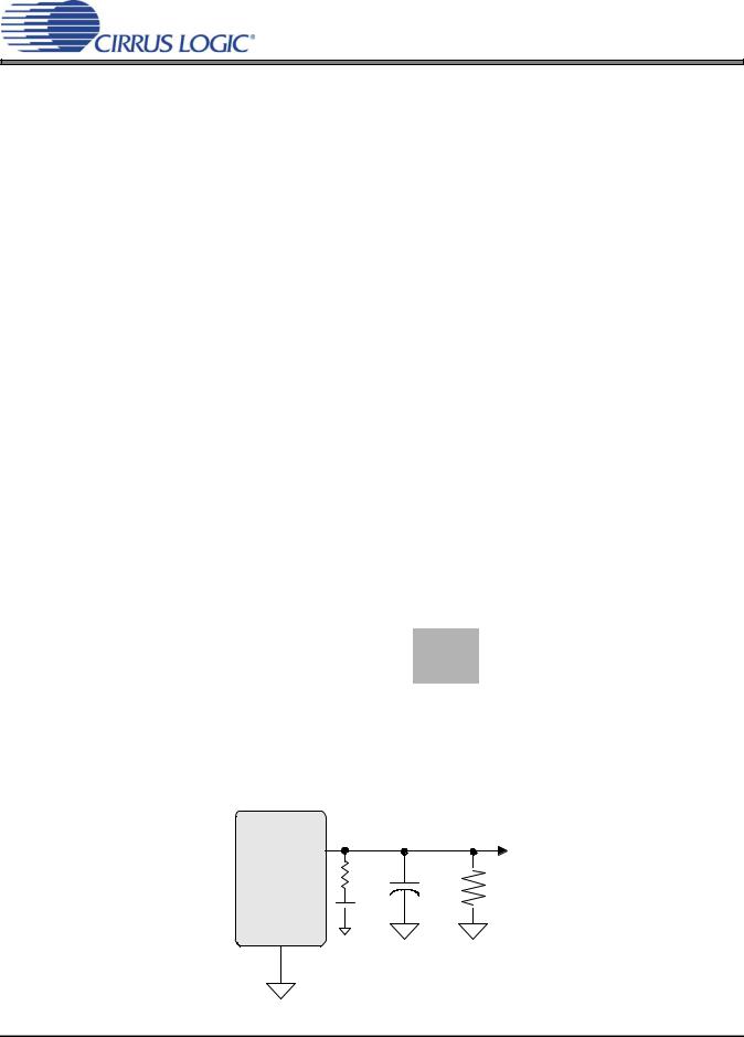
Figure 2. Headphone Output Test Load
14 |
DS792F2 |

CS43L22
LINE OUTPUT VOLTAGE LEVEL CHARACTERISTICS
Test conditions (unless otherwise specified): Input test signal is a full-scale 997 Hz sine wave; measurement bandwidth is 20 Hz to 20 kHz; Sample Frequency = 48 kHz; Test load RL = 10 kΩ, CL = 10 pF (see Figure 2); “Required Initialization Settings” on
page 32 written on power up.
|
Parameters |
|
|
VA = 2.5V |
|
|
|
VA = 1.8V |
|
|
Unit |
|||
|
|
|
|
|
Min |
Typ |
Max |
|
Min |
Typ |
Max |
|
|
|
AOUTx Voltage Into RL = 10 kΩ |
|
|
|
|
|
|
|
|
|
|
|
|||
HP_GAIN[2:0] |
|
Analog |
|
VHP |
|
|
|
|
|
|
|
|
|
|
|
|
Gain (G) |
|
|
|
|
|
|
|
|
|
|
|
|
000 |
|
0.3959 |
|
1.8 V |
- |
1.34 |
- |
|
- |
0.97 |
- |
|
|
Vpp |
|
|
|
|
2.5 V |
- |
1.34 |
- |
|
- |
0.97 |
- |
|
|
Vpp |
001 |
|
0.4571 |
|
1.8 V |
- |
1.55 |
- |
|
- |
1.12 |
- |
|
|
Vpp |
|
|
|
|
2.5 V |
- |
1.55 |
- |
|
- |
1.12 |
- |
|
|
Vpp |
010 |
|
0.5111 |
|
1.8 V |
- |
1.73 |
- |
|
- |
1.25 |
- |
|
|
Vpp |
|
|
|
|
2.5 V |
- |
1.73 |
- |
|
- |
1.25 |
- |
|
|
Vpp |
011 (default) |
|
0.6047 |
|
1.8 V |
- |
2.05 |
- |
|
1.41 |
1.48 |
1.55 |
|
|
Vpp |
|
|
|
|
2.5 V |
1.95 |
2.05 |
2.15 |
|
- |
1.48 |
- |
|
|
Vpp |
100 |
|
0.7099 |
|
1.8 V |
- |
2.41 |
- |
|
- |
1.73 |
- |
|
|
Vpp |
|
|
|
|
2.5 V |
- |
2.41 |
- |
|
- |
1.73 |
- |
|
|
Vpp |
101 |
|
0.8399 |
|
1.8 V |
- |
2.85 |
- |
|
|
2.05 |
|
|
|
Vpp |
|
|
|
|
2.5 V |
- |
2.85 |
- |
|
- |
2.05 |
- |
|
|
Vpp |
110 |
|
1.0000 |
|
1.8 V |
- |
3.39 |
- |
|
- |
2.44 |
- |
|
|
Vpp |
|
|
|
|
2.5 V |
- |
3.39 |
- |
|
- |
2.44 |
- |
|
|
Vpp |
111 |
|
1.1430 |
|
1.8 V |
|
(See (Note 8) |
|
|
|
2.79 |
|
|
|
Vpp |
|
|
|
|
2.5 V |
- |
3.88 |
- |
|
- |
2.79 |
- |
|
|
Vpp |
COMBINED DAC INTERPOLATION & ON-CHIP ANALOG FILTER RESPONSE |
||||||||||||||
|
|
|
|
|
|
|
|
|
|
|
||||
|
|
Parameters (Note 9) |
|
|
|
Min |
Typ |
Max |
|
Unit |
||||
Frequency Response 10 Hz to 20 kHz |
|
|
|
-0.01 |
- |
+0.08 |
|
|
dB |
|||||
|
|
|
|
|
|
|
|
|
|
|
|
|
||
Passband |
|
|
|
|
|
to -0.05 dB corner |
0 |
- |
0.4780 |
|
|
Fs |
||
|
|
|
|
|
|
to -3 dB corner |
0 |
- |
0.4996 |
|
|
Fs |
||
StopBand |
|
|
|
|
|
|
|
0.5465 |
- |
- |
|
|
Fs |
|
|
|
|
|
|
|
|
|
|
|
|
||||
StopBand Attenuation (Note 10) |
|
|
|
|
50 |
- |
- |
|
|
dB |
||||
|
|
|
|
|
|
|
|
|
|
|
|
|
|
|
Group Delay |
|
|
|
|
|
|
|
- |
9/Fs |
- |
|
|
s |
|
|
|
|
|
|
|
|
|
|
|
|||||
De-emphasis Error |
|
|
Fs = 32 kHz |
- |
- |
+1.5/+0 |
|
|
dB |
|||||
|
|
|
|
|
|
Fs = 44.1 kHz |
- |
- |
+0.05/-0.25 |
|
dB |
|||
|
|
|
|
|
|
Fs = 48 kHz |
- |
- |
-0.2/-0.4 |
|
|
dB |
||
9.Response is clock dependent and will scale with Fs. Note that the response plots (Figures 22 and 25 on page 63) have been normalized to Fs and can be de-normalized by multiplying the X-axis scale by Fs.
10.Measurement Bandwidth is from Stopband to 3 Fs.
DS792F2 |
15 |
CS43L22
SWITCHING SPECIFICATIONS - SERIAL PORT
Inputs: Logic 0 = DGND; Logic 1 = VL.
|
|
Parameters |
|
Symbol |
Min |
Max |
Units |
|
|
pin Low Pulse Width |
(Note 11) |
|
1 |
- |
ms |
|
RESET |
|
|||||
|
MCLK Frequency (Note 12) |
|
|
(See “Serial Port Clock- |
MHz |
||
|
|
|
|
|
ing” on page 29) |
|
|
|
MCLK Duty Cycle |
|
|
45 |
55 |
% |
|
|
Slave Mode |
|
|
|
|
|
|
|
Sample Rate (LRCK) |
|
Fs |
(See “Serial Port Clock- |
kHz |
||
|
|
|
|
|
ing” on page 29) |
|
|
|
LRCK Duty Cycle |
|
|
45 |
55 |
% |
|
|
SCLK Frequency |
|
1/tP |
- |
64•Fs |
Hz |
|
|
SCLK Duty Cycle |
|
|
45 |
55 |
% |
|
|
LRCK Setup Time Before SCLK Rising Edge |
|
ts(LK-SK) |
40 |
- |
ns |
|
|
SDIN Setup Time Before SCLK Rising Edge |
|
ts(SD-SK) |
20 |
- |
ns |
|
|
SDIN Hold Time After SCLK Rising Edge |
|
th |
20 |
- |
ns |
|
|
Master Mode |
|
|
|
|
|
|
|
Sample Rate (LRCK) |
|
Fs |
(See “Serial Port Clock- |
Hz |
||
|
|
|
|
|
ing” on page 29) |
|
|
|
LRCK Duty Cycle |
|
|
45 |
55 |
% |
|
|
SCLK Frequency |
SCLK=MCLK mode |
1/tP |
- |
12.0000 |
MHz |
|
|
|
|
MCLK=12.0000 MHz |
1/tP |
- |
68•Fs |
Hz |
|
|
|
all other modes |
1/tP |
- |
64•Fs |
Hz |
|
SCLK Duty Cycle |
|
|
45 |
55 |
% |
|
|
SDIN Setup Time Before SCLK Rising Edge |
|
ts(SD-SK) |
20 |
- |
ns |
|
|
SDIN Hold Time After SCLK Rising Edge |
|
th |
20 |
- |
ns |
|
11.After powering up the CS43L22, RESET should be held low after the power supplies and clocks are settled.
12.See “Example System Clock Frequencies” on page 61 for typical MCLK frequencies.
|
|
|
|
|
|
|
|
|
|
|
|
|
|
|
|
|
|
|
|
|
// |
|
|
|
|
|
|
|
|
|
|
|
|
|
|
|
|
|
|
|
|
LRCK |
|
|
|
|
|
|
|
|
|
|
|
|
|
|
|
|
|
|
|
|
|
|
|
|
|
|
|
|
|
|
|
|
|
|
|
|
|
||||
|
|
|
|
|
|
|
|
|
|
|
|
|
|
|
|
|
|
|
|
|
|
|
|
|
|
|
|
|
|
|
|
|
|
|
|
|
|
|
|||
|
|
|
|
|
|
|
|
|
|
|
|
|
|
|
|
|
|
|
|
|
// |
|
|
|
|
|
|
|
|
|
|
|
|
|
|
|
|
|
|
|
|
|
|
|
|
|
|
|
|
|
|
|
|
|
|
|
|
|
|
|
|
|
|
|
|
|
|
|
|
|
|
|
|
|
|
|
|
|
|
|
|
||
|
|
|
|
|
|
|
|
|
ts(LK-SK) |
|
|
|
|
|
|
|
|
|
|
|
tP |
|
|
|
|
|
|
||||||||||||||
|
|
|
|
|
|
|
|
|
|
|
|
|
|
|
|
|
|
|
|
|
|
|
|
|
|
|
|
|
|
|
|
|
|
|
|
|
|
|
|
|
|
SCLK |
|
|
|
|
|
|
|
|
|
|
|
|
|
|
|
|
|
// |
|
|
|
|
|
|
|
|
|
|
|
|
|
|
|
|
|
|
|
|
|||
|
|
|
|
|
|
|
|
|
|
|
|
|
|
|
|
|
|
|
|
|
|
|
|
|
|
|
|
|
|
|
|
|
|
|
|
||||||
|
|
|
|
|
|
|
|
|
|
|
|
|
|
|
|
|
|
|
|
|
|
|
|
|
|
|
|
|
|
|
|
|
|
|
|
|
|
||||
|
|
|
|
|
|
|
|
|
|
|
|
|
|
|
|
|
|
|
|
|
|
|
|
|
|
|
|
|
// |
|
|
|
|
|
|
|
|
|
|
|
|
|
|
|
|
|
|
|
|
|
|
|
|
|
|
|
|
|
|
|
|
|
|
|
|
|
|
|
|
|
|
|
|
|
|
|
|||||||
|
|
|
|
|
|
|
|
|
|
|
|
|
|
|
|
|
|
|
|
|
|
|
|
|
|
|
|
|
|
|
|
|
|
|
|||||||
|
|
|
|
|
|
|
|
|
|
|
ts(SD-SK) |
|
|
|
|
|
|
|
|
|
|
th |
|
|
|
|
|
||||||||||||||
|
|
|
|
|
|
|
|
|
|
|
|
// |
|
|
|
|
|
|
|
|
|
||||||||||||||||||||
|
|
|
|
|
|
|
|
|
|
|
|
|
|
|
|
|
|
|
|
|
|
|
|
|
|
|
|
|
|
|
|
|
|
|
|
|
|
|
|
||
SDIN |
|
|
|
|
|
|
|
|
|
|
|
|
|
|
|
|
|
|
|
|
|
|
|
|
|
|
|
|
|
|
|
MSB-1 |
|||||||||
|
|
|
|
|
|
|
|
|
|
|
|
MSB |
|
|
|
|
|
|
|
|
|
|
|
|
|
|
|
|
|
|
|||||||||||
|
|
|
|
|
|
|
|
|
|
|
|
|
|
|
|
|
|
|
|
// |
|
|
|
|
|
|
|
|
|
|
|
|
|
|
|
|
|
|
|
|
|
|
|
|
|
|
|
|
|
|
|
|
|
|
|
|
|
|
|
|
|
|
|
|
|
|
|
|
|
|
|
|
|
|
|
|
|
|
|
|
|
||
|
|
|
|
|
|
|
|
|
|
|
|
|
|
|
|
|
|
|
|
|
|
|
|
|
|
|
|
|
|
|
|
|
|
|
|
|
|
|
|
|
|
Figure 3. Serial Audio Interface Timing
16 |
DS792F2 |
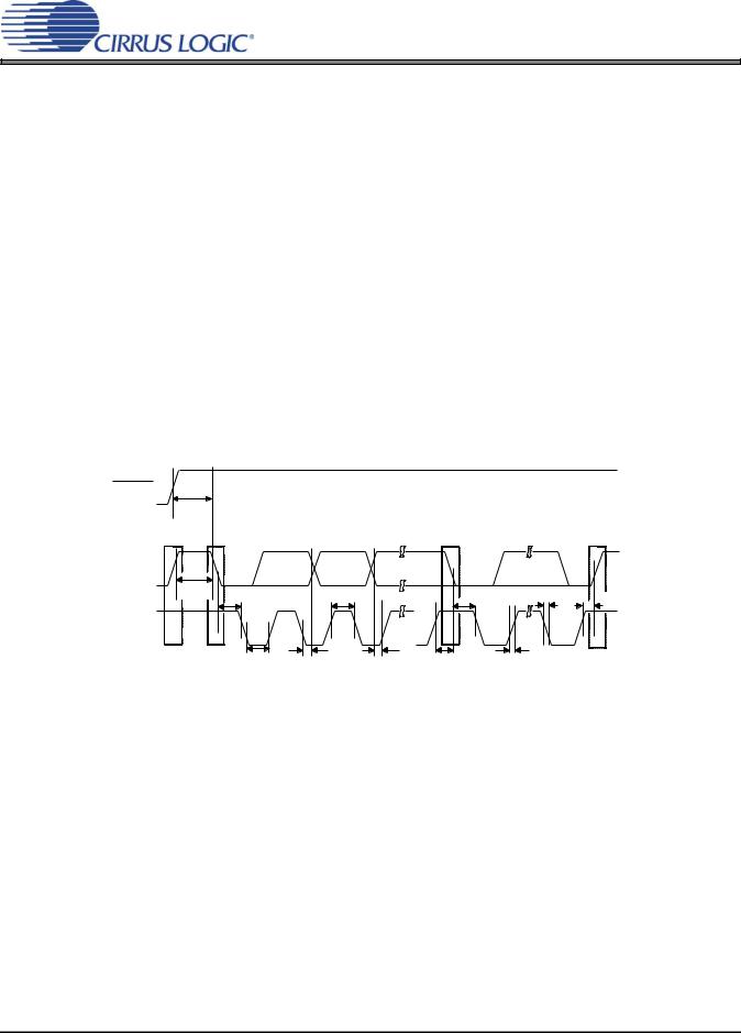
CS43L22
SWITCHING SPECIFICATIONS - I²C CONTROL PORT
Inputs: Logic 0 = DGND; Logic 1 = V; SDA CL = 30 pF.
|
|
Parameters |
|
Symbol |
Min |
Max |
Unit |
|
SCL Clock Frequency |
|
fscl |
- |
100 |
kHz |
|
|
|
Rising Edge to Start |
|
tirs |
550 |
- |
ns |
|
RESET |
|
|||||
|
Bus Free Time Between Transmissions |
|
tbuf |
4.7 |
- |
µs |
|
|
Start Condition Hold Time (prior to first clock pulse) |
|
thdst |
4.0 |
- |
µs |
|
|
Clock Low time |
|
tlow |
4.7 |
- |
µs |
|
|
Clock High Time |
|
thigh |
4.0 |
- |
µs |
|
|
Setup Time for Repeated Start Condition |
|
tsust |
4.7 |
- |
µs |
|
|
SDA Hold Time from SCL Falling |
(Note 13) |
thdd |
0 |
- |
µs |
|
|
SDA Setup time to SCL Rising |
|
tsud |
250 |
- |
ns |
|
|
Rise Time of SCL and SDA |
|
trc |
- |
1 |
µs |
|
|
Fall Time SCL and SDA |
|
tfc |
- |
300 |
ns |
|
|
Setup Time for Stop Condition |
|
tsusp |
4.7 |
- |
µs |
|
|
Acknowledge Delay from SCL Falling |
|
tack |
300 |
1000 |
ns |
|
13. Data must be held for sufficient time to bridge the transition time, tfc, of SCL.
RESET |
|
|
|
|
|
|
t irs |
|
|
|
Repeated |
|
|
Stop |
Start |
|
|
|
Stop |
|
|
|
Start |
|
|||
SDA |
|
|
|
|
|
|
t buf |
t hdst |
t high |
|
t hdst |
t f |
susp |
SCL |
|
|
|
|
|
|
|
t low |
t hdd |
t sud |
tsust |
t r |
|
Figure 4. Control Port Timing - I²C
DS792F2 |
17 |

CS43L22
DC ELECTRICAL CHARACTERISTICS
AGND = 0 V; all voltages with respect to ground.
Parameters |
|
Min |
Typ |
Max |
Units |
VQ Characteristics |
|
|
|
|
|
|
|
|
|
|
|
Nominal Voltage |
|
- |
0.5•VA |
- |
V |
Output Impedance |
|
- |
23 |
- |
kΩ |
DC Current Source/Sink |
|
- |
- |
1 |
μA |
|
|
|
|
|
|
Power Supply Rejection Ratio Characteristics |
|
|
|
|
|
|
|
|
|
|
|
PSRR @ 1 kHz (Note 14) |
DAC (HP & Line Amps) |
- |
60 |
- |
dB |
|
|
|
|
|
|
PSRR @ 60 Hz (Note 14) |
DAC (HP & Line Amps) |
- |
60 |
- |
dB |
|
|
|
|
|
|
PSRR @ 217 Hz |
Full-Bridge PWM Outputs |
- |
56 |
- |
dB |
|
|
|
|
|
|
14.Valid with the recommended capacitor values on FILT+ and VQ. Increasing the capacitance will also increase the PSRR.
DIGITAL INTERFACE SPECIFICATIONS & CHARACTERISTICS
Parameters (Note 15) |
|
|
Symbol |
Min |
Max |
Units |
Input Leakage Current |
|
|
Iin |
- |
±10 |
μA |
Input Capacitance |
|
|
|
- |
10 |
pF |
|
|
|
|
|
|
|
1.8 V - 3.3 V Logic |
|
|
|
|
|
|
High-Level Output Voltage (IOH = -100 μA) |
|
|
VOH |
VL - 0.2 |
- |
V |
Low-Level Output Voltage (IOL = 100 μA) |
|
|
VOL |
- |
0.2 |
V |
High-Level Input Voltage |
VL = 1.65 |
V |
VIH |
0.85•VL |
- |
V |
|
VL = 1.8 |
V |
|
0.77•VL |
- |
V |
|
VL = 2.0 |
V |
|
0.68•VL |
- |
V |
|
VL > 2.0 |
V |
|
0.65•VL |
- |
V |
|
|
|
|
|
|
|
Low-Level Input Voltage |
|
|
VIL |
- |
0.30•VL |
V |
15. See “I/O Pin Characteristics” on page 8 for serial and control port power rails.
18 |
DS792F2 |
|
|
|
|
|
|
|
|
|
|
|
|
CS43L22 |
|||
|
|
|
|
|
|
|
|
|
|
|
|
|
|
|
|
POWER CONSUMPTION See (Note 16) |
|
|
|
|
|
|
|
|
|
|
|
||||
|
|
|
|
|
|
|
|
|
|
|
|
|
|
||
|
Operation |
Register Settings |
|
|
|
Typical Current (mA) |
|
|
|
|
|||||
|
02h |
|
04h |
|
|
iVHP |
iVA |
iVD |
iVL |
iVP |
|
|
|
||
|
|
PDN[7:0] |
HPB[1:0]PDN |
HPA[1:0]PDN |
SPKB[1:0]PDN |
SPKA[1:0]PDN |
|
|
|
Total |
|||||
|
|
|
|
|
|
VL=3.3V |
VP=3.7V |
|
|
Power |
|||||
|
|
|
|
|
|
|
|
|
|
|
(Note 19) |
|
|
(mWrms) |
|
|
|
|
|
|
|
|
|
|
|
|
|
|
|
||
|
|
|
|
|
|
|
V |
|
|
|
|
|
|
|
|
1 |
Off (Note 17) |
x |
x |
x |
x |
x |
1.8 |
0.00 |
0.00 |
0.00 |
0.00 |
0.00 |
|
|
0.00 |
|
|
|
|
|
|
|
2.5 |
0.00 |
0.00 |
0.00 |
|
|
0.00 |
||
|
|
|
|
|
|
|
|
|
|
|
|||||
2 |
Standby (Note 18) |
0x9F |
x |
x |
x |
x |
1.8 |
0.00 |
0.00 |
0.01 |
0.00 |
0.00 |
|
|
0.02 |
|
|
|
|
|
|
|
2.5 |
0.00 |
0.00 |
0.02 |
|
|
0.05 |
||
|
|
|
|
|
|
|
|
|
|
|
|||||
3 |
Stereo Passthrough to Headphone |
0x9E |
10 |
10 |
11 |
11 |
1.8 |
2.79 |
1.91 |
1.06 |
0.01 |
0.00 |
|
|
10.39 |
|
|
|
|
|
|
|
2.5 |
3.18 |
2.14 |
1.81 |
|
|
17.85 |
||
|
|
|
|
|
|
|
|
|
|
|
|||||
4 |
Mono Playback to Headphone |
0x9E |
10 |
11 |
11 |
11 |
1.8 |
1.59 |
1.99 |
2.72 |
0.01 |
0.00 |
|
|
11.36 |
|
|
|
|
|
|
|
2.5 |
2.07 |
2.62 |
4.27 |
|
|
22.43 |
||
|
|
|
|
|
|
|
|
|
|
|
|||||
5 |
Stereo Playback to Headphone |
0x9E |
10 |
10 |
11 |
11 |
1.8 |
2.77 |
2.00 |
2.91 |
0.01 |
0.00 |
|
|
13.84 |
|
|
|
|
|
|
|
2.5 |
3.27 |
2.63 |
4.28 |
|
|
25.48 |
||
|
|
|
|
|
|
|
|
|
|
|
|||||
6 |
Mono Playback to Speaker |
0x9E |
11 |
11 |
10 |
10 |
1.8 |
0.00 |
0.20 |
4.42 |
0.01 |
1.00 |
|
|
12.05 |
|
|
|
|
|
|
|
2.5 |
0.00 |
0.22 |
6.77 |
|
|
21.21 |
||
|
|
|
|
|
|
|
|
|
|
|
|||||
7 |
Stereo Playback to Speaker |
0x9E |
11 |
11 |
10 |
10 |
1.8 |
0.00 |
0.20 |
4.38 |
0.01 |
1.00 |
|
|
11.98 |
|
|
|
|
|
|
|
2.5 |
0.00 |
0.22 |
6.80 |
|
|
21.28 |
||
|
|
|
|
|
|
|
|
|
|
|
|||||
|
16. Unless otherwise noted, test conditions are as |
follows: All zeros input, Slave Mode, |
sample |
||||||||||||
|
rate = 48 kHz; No load. Digital (VD) and logic (VL) supply current will vary depending on speed mode |
||||||||||||||
|
and master/slave operation.“Required Initialization Settings” on page 32 written on power up. |
|
|||||||||||||
17.RESET pin 25 held LO, all clocks and data lines are held LO.
18.RESET pin 25 held HI, all clocks and data lines are held HI.
19.VL current will slightly increase in Master Mode.
DS792F2 |
19 |

CS43L22
4. APPLICATIONS
4.1Overview
4.1.1Basic Architecture
The CS43L22 is a highly integrated, low power, 24-bit audio DAC comprised of a Digital Signal Processing Engine, headphone amplifiers, a digital PWM modulator and two full-bridge power back-ends. Other features include battery level monitoring and compensation and temperature monitoring. The DAC is designed using multi-bit delta-sigma techniques and operates at an oversampling ratio of 128Fs, where Fs is equal to the system sample rate.
The PWM modulator operates at a fixed frequency of 384 kHz. The power MOSFETs are configured for either stereo full-bridge or mono parallel full bridge output. The DAC operates in one of four sample rate speed modes: Quarter, Half, Single and Double. It accepts and is capable of generating serial port clocks (SCLK, LRCK) derived from an input Master Clock (MCLK).
4.1.2Line Inputs
4 pairs of stereo analog inputs are provided for applications that require analog passthrough directly to the HP/Line amplifiers. This analog input portion allows selection from and configuration of multiple combinations of these stereo sources.
4.1.3Line & Headphone Outputs
The analog output portion of the CS43L22 includes a headphone amplifier capable of driving headphone and line-level loads. An on-chip charge pump creates a negative headphone supply allowing a full-scale output swing centered around ground. This eliminates the need for large DC-Blocking capacitors and allows the amplifier to deliver more power to headphone loads at lower supply voltages.
4.1.4Speaker Driver Outputs
The Class D power amplifiers drive 8 Ω (stereo) and 4 Ω (mono) speakers directly, without the need for an external filter. The power MOSFETS are powered directly from a battery eliminating the efficiency loss associated with an external regulator. Battery level monitoring and compensation maintains a steady output as battery levels fall. A temperature monitor continually measures the die temperature and registers when predefined thresholds are exceeded. NOTE: The CS43L22 should only be used in captive speaker systems where the outputs are permanently tied to the speaker terminals.
4.1.5Fixed Function DSP Engine
The fixed-function digital signal processing engine processes the PCM serial input data. Independent volume control, left/right channel swaps, mono mixes, tone control and limiting functions also comprise the DSP engine.
4.1.6Beep Generator
The beep generator delivers tones at select frequencies across approximately two octave major scales. With independent volume control, beeps may be configured to occur continuously, periodically, or at single time intervals.
4.1.7Power Management
Two control registers provide independent power-down control of the DAC, Headphone and Speaker output blocks in the CS43L22 allowing operation in select applications with minimal power consumption.
20 |
DS792F2 |
Loading...