


 Loading...
CS4207
Low-power, 4-in / 6-out HD Audio Codec with Headphone Amp
DIGITAL to ANALOG FEATURES
DAC1 (Headphone)
–101 dB Dynamic Range (A-wtd)
–-89 dB THD+N
Headphone Amplifier - GND Centered
–Integrated Negative-voltage Regulator
–No DC-blocking Capacitor Required
–50 mW Power/Channel into 16
DAC2 & DAC3 (Line Outs)
–110 dB Dynamic Range (A-wtd)
–-94 dB THD+N
–Differential Balanced or Single-ended
Each DAC Supports 32 kHz to 192 kHz Sample Rates Independently.
Digital Volume Control
–+6.0 dB to -57.5 dB in 0.5 dB Steps
–Zero Cross and/or Soft Ramp Transitions
Independent Support of D0 and D3 Power States for Each DAC
Fast D3 to D0 Transition
–Audio Playback in Less Than 50 ms
ANALOG to DIGITAL FEATURES
ADC1 & ADC2
–105 dB Dynamic Range (A-wtd)
–-88 dB THD+N
–Differential Balanced or Single-ended Inputs
–Analog Programmable Gain Amplifier (PGA) ±12 dB, 1.0 dB Steps, with Zero Cross Transitions and Mute
MIC Inputs
–Pre-amplifier with Selectable 0 dB, +10 dB, +20 dB, and +30 dB Gain Settings
–Programmable, Low-noise MIC Bias Level
Each ADC Supports 8 kHz to 96 kHz Sample Rates Independently
Additional Digital Attenuation Control
–-13.0 dB to -51.0 dB in 1.0 dB steps
–Zero Cross and/or Soft Ramp Transitions
Digital Interface for Two Dual Digital Mic Inputs
Independent Support of D0 and D3 Power States for Each ADC
VD |
VA, VA_REF |
VA_HP |
(1.5 V to 1.8 V) |
(3.3 V to 5.0 V) |
(3.3 V to 5.0 V) |
|
|
|
|
|
|
|
Chrg |
|
|
|
|
|
|
|
|
|
Pump |
|
|
|
|
|
|
|
|
|
Buck |
|
|
|
|
|
|
|
SRC & |
|
+VHP |
-VHP |
|
|
Translator |
|
|
Vol/Mute |
2-Chnl |
|
|
Left HP Out |
|
Bus |
Interface |
SRC & |
Line |
|
- Left Line Out |
||||
2-Chnl |
|
||||||||
|
|
|
|
Multibit |
DAC1 |
|
|
Right HP Out |
|
HD Audio |
|
HD |
|
|
Modulator |
|
|
||
|
|
|
|
|
|
|
+ |
||
|
Audio |
|
|
|
|
|
|
||
(1.5 V to 3.3 V) |
Level |
|
|
Modulator |
|
|
|
||
|
|
Vol/Mute |
|
|
|
- Right Line Out |
|||
VL_HD |
|
|
|
Multibit |
DAC2 |
Out |
|
+ |
|
|
|
|
|
|
|
||||
|
|
|
|
|
SRC & |
2-Chnl |
Line |
|
+Left Line Out |
|
|
|
|
Vol/Mute |
Multibit |
|
- |
||
GPIO |
|
GPIO |
|
DAC3 |
Out |
|
+ |
||
|
|
|
Modulator |
|
|||||
|
|
SPDIF |
|
|
|
|
|
- Right Line Out |
|
S/PDIF OUT 2 |
|
|
|
|
|
|
|
+ |
|
|
TX 2 |
|
Vol/Boost/ |
Digital |
2-Chnl |
|
|
||
|
Translator |
SPDIF |
|
Filter & |
PGA |
- Line/Mic In L |
|||
|
|
Mute |
ADC1 |
Line/Mic In R |
|||||
VL_IF |
|
SRC |
|
|
|||||
Fs |
|
|
|
|
|
+ |
|||
S/PDIF OUT 1 |
|
TX 1 |
|
|
|
|
|
+ |
|
|
|
HD Bus |
128Fs Clock |
|
|
|
|
|
|
(3.3 V) |
Level |
|
Vol/Boost/ |
Digital |
2-Chnl |
|
|
- Mic/Line In L |
|
|
Multiplier |
PGA |
|||||||
|
|
Mute |
SRC |
ADC2 |
+Mic/Line In R |
||||
|
|
|
|
Filter & |
|
|
|||
S/PDIF IN |
|
SPDIF |
SPDIF |
|
|
|
MIC |
|
- |
|
RX |
RX SRC |
|
|
|
|
Mic Bias |
||
|
|
|
|
|
|
||||
D-Mic Clock |
|
|
|
|
|
Jack |
Bias |
|
|
|
|
|
|
|
|
|
SENSE_A |
||
D-Mic In |
|
|
|
|
|
Sense |
|
|
|
|
|
|
|
|
|
|
|
||
|
Copyright Cirrus Logic, Inc. 2012 |
AUG '12 |
http://www.cirrus.com |
(All Rights Reserved) |
DS880F4 |
|

CS4207
Digital Audio Interface Receiver
Complete EIAJ CP1201, IEC 60958, S/PDIF Compatible Receiver
32 kHz to 192 kHz Sample Rate Range
Automatic Detection of Compressed Audio Streams
Integrated Sample Rate Converter
–128 dB Dynamic Range
–-120 dB THD+N
–Supports Sample Rates up to 192 kHz
–1:1 Input/Output Sample Rate Ratios
Digital Audio Interface Transmitters
Two Independent EIAJ CP1201, IEC-60958, S/PDIF Compatible Transmitters
32 kHz to 192 kHz Sample Rate Range
System Features
Very Low D3 Power Dissipation of <7 mW
–Jack Detect Active in D3
–HDA BITCLK Not Required for D3 State
Jack Detect Does Not Require HDA Bus BITCLK
All Configuration Settings are Preserved in D3 State
Pop/Click Suppression in State Transitions
Detects Wake Event and Generates Power State Change Request when HDA Bus Controller is in D3
Variable Power Supplies
–1.5 V to 1.8 V Digital Core Voltage
–3.3 V to 5.0 V Analog Core Voltage
–3.3 V to 5.0 V Headphone Drivers
–1.5 V to 3.3 V HD Bus Interface Logic
–3.3 V Interface Logic levels for GPIO, S/PDIF, and Digital Mic
Individual Power-down Managed
–ADCs, DACs, PGAs, Headphone Driver, S/PDIF Receiver, and Transmitters
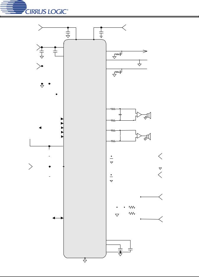
General Description
The CS4207 is a highly integrated multi-channel lowpower HD Audio Codec featuring 192 kHz DACs, 96 kHz ADCs, 192 kHz S/PDIF Transmitters and Receiver, Microphone pre-amp and bias voltage, and a ground centered Headphone driver. Based on multi-bit, delta-sigma modulation, it allows infinite sample rate adjustment between 32 kHz and 192 kHz.
The ADC input path allows control of a number of features. The microphone input path includes a selectable programmable-gain pre-amplifier stage and a low-noise MIC bias voltage supply. A PGA is available for line and microphone inputs and provides analog gain with soft ramp and zero cross transitions. The ADC also features an additional digital volume attenuator with soft ramp transitions.
The stereo headphone amplifier is powered from a separate internally generated positive supply, with an integrated charge pump providing a negative supply. This allows a ground-centered analog output with a wide signal swing and eliminates external DC-blocking capacitors.
The integrated digital audio interface receiver and transmitters utilize a 24-bit, high-performance, monolithic CMOS stereo asynchronous sample rate converter to clock align the PCM samples to/from the S/PDIF interfaces. Auto detection of non-PCM encoded data disables the sample rate conversion to preserve bit accuracy of the data.
In addition to its many features, the CS4207 operates from a low-voltage analog and digital core, making this part ideal for portable systems that require low power consumption in a minimal amount of space.
The CS4207 is available in a 48-pin WQFN package in both Automotive (-40°C to +105°C) and Commercial (-40°C to +85°C) grades. The CS4207 Customer Demonstration board is also available for device evaluation and implementation suggestions. Please refer to “Ordering Information” on p 147 for complete ordering information.
2 |
DS880F4 |

|
|
CS4207 |
TABLE OF CONTENTS |
|
|
1. PIN DESCRIPTIONS .............................................................................................................................. |
8 |
|
1.1 |
CS4207 48-pin QFN Pinout: ............................................................................................................ |
8 |
1.2 |
Digital I/O Pin Characteristics ........................................................................................................ |
10 |
2. TYPICAL CONNECTION DIAGRAMS ................................................................................................. |
11 |
|
3. CHARACTERISTICS AND SPECIFICATIONS .................................................................................... |
13 |
|
RECOMMENDED OPERATING CONDITIONS .................................................................................. |
13 |
|
ABSOLUTE MAXIMUM RATINGS ...................................................................................................... |
13 |
|
ANALOG INPUT CHARACTERISTICS (COMMERCIAL - CNZ) ......................................................... |
14 |
|
ANALOG INPUT CHARACTERISTICS (AUTOMOTIVE - DNZ) ......................................................... |
15 |
|
ADC DIGITAL FILTER CHARACTERISTICS ...................................................................................... |
16 |
|
ANALOG OUTPUT CHARACTERISTICS (COMMERCIAL - CNZ) ..................................................... |
17 |
|
ANALOG OUTPUT CHARACTERISTICS (AUTOMOTIVE - DNZ) ..................................................... |
19 |
|
COMBINED DAC INTERPOLATION & ON-CHIP ANALOG FILTER RESPONSE ............................. |
21 |
|
DC ELECTRICAL CHARACTERISTICS .............................................................................................. |
21 |
|
DIGITAL MICROPHONE INTERFACE CHARACTERISTICS ............................................................. |
22 |
|
DIGITAL INTERFACE SPECIFICATIONS & CHARACTERISTICS .................................................... |
23 |
|
HD AUDIO BUS SPECIFICATIONS & CHARACTERISTICS .............................................................. |
23 |
|
S/PDIF TRANSMITTER/RECEIVER SPECIFICATIONS & CHARACTERISTICS .............................. |
23 |
|
POWER CONSUMPTION ................................................................................................................... |
24 |
|
4. CODEC RESET AND INITIALIZATION .............................................................................................. |
25 |
|
4.1 |
Link Reset ...................................................................................................................................... |
25 |
4.2 |
Function Group Reset .................................................................................................................... |
25 |
4.3 |
Codec Initialization ......................................................................................................................... |
25 |
4.4 |
D3 Lower Power State Support ..................................................................................................... |
26 |
4.5 |
Extended Power States Supported (EPSS) ................................................................................... |
26 |
4.6 |
Power State Settings Reset (PS-SettingsReset) ........................................................................... |
28 |
4.7 |
Register Settings Across Resets ................................................................................................... |
29 |
5. PRESENCE DETECTION ..................................................................................................................... |
31 |
|
5.1 |
Jack Detection Circuit .................................................................................................................... |
31 |
|
5.1.1 Presence Detection and Unsolicited Response .................................................................... |
31 |
|
5.1.2 S/PDIF Receiver Presence Detect ........................................................................................ |
32 |
6. HD AUDIO CODEC SUPPORTED VERBS AND RESPONSES ......................................................... |
33 |
|
6.1 |
Software Programming Model ....................................................................................................... |
33 |
|
6.1.1 Node ID Summary ................................................................................................................. |
34 |
|
6.1.2 Pin Configuration Register Defaults ...................................................................................... |
35 |
6.2 |
Root Node (Node ID = 00h) ........................................................................................................... |
36 |
|
6.2.1 Vendor and Device ID ........................................................................................................... |
36 |
|
6.2.2 Revision ID ............................................................................................................................ |
36 |
|
6.2.3 Subordinate Node Count ....................................................................................................... |
36 |
6.3 |
Audio Function Group (Node ID = 01h) ......................................................................................... |
37 |
|
6.3.1 Subordinate Node Count ....................................................................................................... |
37 |
|
6.3.2 Function Group Type ............................................................................................................. |
37 |
|
6.3.3 Audio Function Group Capabilities ........................................................................................ |
37 |
|
6.3.4 Supported PCM Size, Rates ............................................................................................... |
.. 38 |
|
6.3.5 Supported Stream Formats ................................................................................................... |
39 |
|
6.3.6 Supported Power States ....................................................................................................... |
39 |
|
6.3.7 GPIO Capabilities .................................................................................................................. |
40 |
|
6.3.8 Power States ......................................................................................................................... |
41 |
|
6.3.9 GPIO Data ............................................................................................................................. |
42 |
|
6.3.10 GPIO Enable Mask .............................................................................................................. |
43 |
|
6.3.11 GPIO Direction .................................................................................................................... |
43 |
|
6.3.12 GPIO Sticky Mask ............................................................................................................... |
43 |
DS880F4 |
|
3 |

|
CS4207 |
|
6.3.13 Implementation Identification ............................................................................................... |
|
44 |
6.3.14 Function Reset .................................................................................................................... |
|
44 |
6.4 DAC1, DAC2, DAC3 Output Converter Widgets (Node ID = 02h, 03h, 04h) ................................. |
|
45 |
6.4.1 Audio Widget Capabilities ..................................................................................................... |
|
45 |
6.4.2 Supported PCM Size, Rates ................................................................................................. |
|
46 |
6.4.3 Supported Stream Formats ................................................................................................... |
|
46 |
6.4.4 Supported Power States ....................................................................................................... |
|
47 |
6.4.5 Output Amplifier Capabilities ................................................................................................. |
|
47 |
6.4.6 Power States ......................................................................................................................... |
|
48 |
6.4.7 Converter Stream, Channel ................................................................................................... |
|
49 |
6.4.8 Converter Format .................................................................................................................. |
|
49 |
6.4.9 Amplifier Gain/Mute ............................................................................................................... |
|
51 |
6.5 ADC1, ADC2 Input Converter Widgets (Node ID = 05h, 06h) ....................................................... |
|
53 |
6.5.1 Audio Widget Capabilities ..................................................................................................... |
|
53 |
6.5.2 Supported PCM Size, Rates ................................................................................................. |
|
54 |
6.5.3 Supported Stream Formats ................................................................................................... |
|
54 |
6.5.4 Input Amplifier Capabilities .................................................................................................... |
|
55 |
6.5.5 Connection List Length .......................................................................................................... |
|
55 |
6.5.6 Supported Power States ....................................................................................................... |
|
56 |
6.5.7 ADC1 Connection List Entry .................................................................................................. |
|
56 |
6.5.8 ADC1 Connection Select Control .......................................................................................... |
|
56 |
6.5.9 ADC2 Connection List Entry .................................................................................................. |
|
57 |
6.5.10 ADC2 Connection Select Control ........................................................................................ |
|
57 |
6.5.11 Power States ....................................................................................................................... |
|
58 |
6.5.12 Converter Stream, Channel ................................................................................................. |
|
59 |
6.5.13 Converter Format ................................................................................................................ |
|
59 |
6.5.14 Amplifier Gain/Mute ............................................................................................................. |
|
61 |
6.6 S/PDIF Receiver Input Converter Widget (Node ID = 07h) ........................................................... |
|
63 |
6.6.1 Audio Widget Capabilities ..................................................................................................... |
|
63 |
6.6.2 Supported PCM Size, Rates ................................................................................................. |
|
64 |
6.6.3 Supported Stream Formats ................................................................................................... |
|
64 |
6.6.4 Connection List Length .......................................................................................................... |
|
65 |
6.6.5 Supported Power States ....................................................................................................... |
|
65 |
6.6.6 Connection List Entry ............................................................................................................ |
|
65 |
6.6.7 Power States ......................................................................................................................... |
|
66 |
6.6.8 Converter Stream, Channel ................................................................................................... |
|
67 |
6.6.9 Converter Format .................................................................................................................. |
|
67 |
6.6.10 Digital Converter Control ..................................................................................................... |
|
69 |
6.7 S/PDIF Transmitter 1, S/PDIF Transmitter 2 Output Converter Widgets (Node ID = 08h, 14h) .... |
70 |
|
6.7.1 Audio Widget Capabilities ..................................................................................................... |
|
70 |
6.7.2 Supported PCM Size, Rates ................................................................................................. |
|
71 |
6.7.3 Supported Stream Formats ................................................................................................... |
|
72 |
6.7.4 Supported Power States ....................................................................................................... |
|
72 |
6.7.5 Power States ......................................................................................................................... |
|
72 |
6.7.6 Converter Stream, Channel ................................................................................................... |
|
74 |
6.7.7 Converter Format .................................................................................................................. |
|
74 |
6.7.8 Digital Converter Control ....................................................................................................... |
|
76 |
6.8 Headphone Pin Widget (Node ID = 09h) ....................................................................................... |
|
78 |
6.8.1 Audio Widget Capabilities .................................................................................................. |
... |
78 |
6.8.2 Pin Capabilities ...................................................................................................................... |
|
78 |
6.8.3 Connection List Length .......................................................................................................... |
|
79 |
6.8.4 Supported Power States ....................................................................................................... |
|
79 |
6.8.5 Connection List Entry ............................................................................................................ |
|
80 |
6.8.6 Power States ......................................................................................................................... |
|
80 |
4 |
DS880F4 |
|

|
CS4207 |
6.8.7 Pin Widget Control ................................................................................................................ |
81 |
6.8.8 Unsolicited Response Control ............................................................................................... |
82 |
6.8.9 Pin Sense .............................................................................................................................. |
83 |
6.8.10 Configuration Default ........................................................................................................... |
83 |
6.9 Line Out 1 Pin Widget (Node ID = 0Ah) ......................................................................................... |
85 |
6.9.1 Audio Widget Capabilities ..................................................................................................... |
85 |
6.9.2 Pin Capabilities ...................................................................................................................... |
86 |
6.9.3 Connection List Length .......................................................................................................... |
86 |
6.9.4 Supported Power States ....................................................................................................... |
87 |
6.9.5 Connection List Entry ............................................................................................................ |
87 |
6.9.6 Power States ......................................................................................................................... |
87 |
6.9.7 Pin Widget Control ................................................................................................................ |
88 |
6.9.8 Unsolicited Response Control ............................................................................................... |
89 |
6.9.9 Pin Sense .............................................................................................................................. |
90 |
6.9.10 EAPD/BTL Enable ............................................................................................................... |
90 |
6.9.11 Configuration Default ........................................................................................................... |
91 |
6.10 Line Out 2 Pin Widget (Node ID = 0Bh) ....................................................................................... |
92 |
6.10.1 Audio Widget Capabilities ................................................................................................... |
92 |
6.10.2 Pin Capabilities .................................................................................................................... |
93 |
6.10.3 Connection List Length ........................................................................................................ |
93 |
6.10.4 Connection List Entry .......................................................................................................... |
94 |
6.10.5 Pin Widget Control .............................................................................................................. |
94 |
6.10.6 EAPD/BTL Enable ............................................................................................................... |
95 |
6.10.7 Configuration Default ........................................................................................................... |
96 |
6.11 Line In 1/Mic In 2, Mic In 1/Line In 2 Pin Widgets (Node ID = 0Ch, 0Dh) .................................... |
97 |
6.11.1 Audio Widget Capabilities ................................................................................................... |
97 |
6.11.2 Line In 1/Mic In 2 Pin Capabilities ....................................................................................... |
97 |
6.11.3 Mic In 1/Line In 2 Pin Capabilities ....................................................................................... |
98 |
6.11.4 Input Amplifier Capabilities .................................................................................................. |
99 |
6.11.5 Supported Power States ..................................................................................................... |
99 |
6.11.6 Power States ....................................................................................................................... |
99 |
6.11.7 Line In 1/Mic In 2 Pin Widget Control ................................................................................ |
101 |
6.11.8 Mic In 1/Line In 2 Pin Widget Control ................................................................................ |
101 |
6.11.9 Unsolicited Response Control ........................................................................................... |
102 |
6.11.10 Pin Sense ........................................................................................................................ |
103 |
6.11.11 Mic In 1/Line In 2 EAPD/BTL Enable .............................................................................. |
104 |
6.11.12 Line In 1/Mic In 2 Configuration Default .......................................................................... |
104 |
6.11.13 Mic In 1/Line In 2 Configuration Default .......................................................................... |
105 |
6.11.14 Amplifier Gain/Mute ......................................................................................................... |
106 |
6.12 Digital Mic In 1, Digital Mic In 2 Pin Widgets (Node ID = 0Eh, 12h) ........................................... |
108 |
6.12.1 Audio Widget Capabilities ................................................................................................. |
108 |
6.12.2 Pin Capabilities .................................................................................................................. |
109 |
6.12.3 Input Amplifier Capabilities ................................................................................................ |
109 |
6.12.4 Pin Widget Control ............................................................................................................ |
110 |
6.12.5 Digital Mic In 1 Configuration Default ................................................................................ |
110 |
6.12.6 Digital Mic In 2 Configuration Default ................................................................................ |
111 |
6.12.7 Amplifier Gain/Mute ........................................................................................................... |
112 |
6.13 S/PDIF Receiver Input Pin Widget (Node ID = 0Fh) .................................................................. |
114 |
6.13.1 Audio Widget Capabilities ................................................................................................. |
114 |
6.13.2 Pin Capabilities .................................................................................................................. |
115 |
6.13.3 Supported Power States ................................................................................................... |
115 |
6.13.4 Power States ..................................................................................................................... |
116 |
6.13.5 Pin Widget Control ............................................................................................................ |
117 |
6.13.6 Unsolicited Response Control ........................................................................................... |
117 |
DS880F4 |
5 |

|
CS4207 |
6.13.7 Pin Sense .......................................................................................................................... |
118 |
6.13.8 Configuration Default ......................................................................................................... |
119 |
6.14 S/PDIF Transmitter 1, S/PDIF Transmitter 2 Output Pin Widgets (Node ID = 10h, 15h) |
........... 120 |
6.14.1 Audio Widget Capabilities ................................................................................................. |
120 |
6.14.2 Pin Capabilities .................................................................................................................. |
121 |
6.14.3 Connection List Length ...................................................................................................... |
121 |
6.14.4 S/PDIF Transmitter 1 Connection List Entry ..................................................................... |
122 |
6.14.5 S/PDIF Transmitter 2 Connection List Entry ..................................................................... |
122 |
6.14.6 Pin Widget Control ............................................................................................................ |
123 |
6.14.7 S/PDIF Transmitter 1 Configuration Default ...................................................................... |
124 |
6.14.8 S/PDIF Transmitter 2 Configuration Default ...................................................................... |
125 |
6.15 Vendor Processing Widget (Node ID = 11h) .............................................................................. |
126 |
6.15.1 Audio Widget Capabilities ................................................................................................. |
126 |
6.15.2 Processing Capabilities ..................................................................................................... |
126 |
6.15.3 Processing State ............................................................................................................... |
127 |
6.15.4 Coefficient Index ................................................................................................................ |
127 |
6.15.5 Processing Coefficient ....................................................................................................... |
128 |
6.15.6 Coefficient Registers ......................................................................................................... |
128 |
6.15.6.1 S/PDIF RX/TX Interface Status (CIR = 0000h) ...................................................... |
129 |
6.15.6.2 S/PDIF RX/TX Interface Control (CIR = 0001h) .................................................... |
130 |
6.15.6.3 ADC Configuration (CIR = 0002h) ......................................................................... |
131 |
6.15.6.4 DAC Configuration (CIR = 0003h) ......................................................................... |
134 |
6.15.6.5 Beep Configuration (CIR = 0004h) ........................................................................ |
135 |
6.16 Beep Generator Widget (Node ID = 13h) .................................................................................. |
136 |
6.16.1 Audio Widget Capabilities ................................................................................................. |
136 |
6.16.2 Beep Generation Control ................................................................................................... |
137 |
7. APPLICATIONS ................................................................................................................................. |
138 |
7.1 HD Audio Interface ....................................................................................................................... |
138 |
7.1.1 Multi-Channel Streams ........................................................................................................ |
138 |
7.2 Analog Inputs ............................................................................................................................... |
139 |
7.3 Analog Outputs ............................................................................................................................ |
142 |
7.3.1 Output Filter ......................................................................................................................... |
142 |
7.3.2 Analog Supply Removal ...................................................................................................... |
142 |
7.4 Digital Mic Inputs .......................................................................................................................... |
142 |
7.5 S/PDIF Input and Outputs ............................................................................................................ |
143 |
7.5.1 S/PDIF Receiver SRC ......................................................................................................... |
143 |
8. PCB LAYOUT CONSIDERATIONS ................................................................................................... |
144 |
8.1 Power Supply, Grounding ............................................................................................................ |
144 |
8.2 QFN Thermal Pad ........................................................................................................................ |
144 |
9. PARAMETER DEFINITIONS .............................................................................................................. |
145 |
10. QFN PACKAGE DIMENSIONS ........................................................................................................ |
146 |
THERMAL CHARACTERISTICS ....................................................................................................... |
146 |
11. ORDERING INFORMATION ............................................................................................................ |
147 |
12. REFERENCES .................................................................................................................................. |
147 |
13. REVISION HISTORY ........................................................................................................................ |
148 |
6 |
DS880F4 |

|
CS4207 |
LIST OF FIGURES |
|
Figure 1.Typical Connection Diagram - Desktop System ......................................................................... |
11 |
Figure 2.Typical Connection Diagram - Portable System ......................................................................... |
12 |
Figure 3.Output Test Load, Headphone Out ............................................................................................. |
18 |
Figure 4.Output Test Load, Line Out ......................................................................................................... |
18 |
Figure 5.Output Test Load, Headphone Out ............................................................................................. |
20 |
Figure 6.Output Test Load, Line Out ......................................................................................................... |
20 |
Figure 7.Digital MIC Interface Timing ........................................................................................................ |
22 |
Figure 8.PS-SettingsReset Behavior ........................................................................................................ |
28 |
Figure 9.Jack Presence Detect Circuit ...................................................................................................... |
31 |
Figure 10.Software Programming Model .................................................................................................. |
33 |
Figure 11.Single-Ended Input Filter ........................................................................................................ |
139 |
Figure 12.Pseudo-Differential Input Filter ............................................................................................... |
140 |
Figure 13.Differential Input Filter ............................................................................................................. |
141 |
Figure 14.Differential to Single-Ended Output Filter ............................................................................... |
142 |
Figure 15.Passive Single-Ended Output Filter ........................................................................................ |
142 |
LIST OF TABLES |
|
Table 1. Register Settings Across Reset Conditions ................................................................................ |
29 |
Table 2. Device Node ID Summary ........................................................................................................... |
34 |
Table 3. Pin Configuration Register Defaults ............................................................................................ |
35 |
Table 4. Stream Format Examples ......................................................................................................... |
138 |
Table 5. Line In 1/Mic In 2 Input Topology Register Settings .................................................................. |
139 |
Table 6. Mic In 1/Line In 2 Input Topology Register Settings .................................................................. |
139 |
DS880F4 |
7 |
CS4207
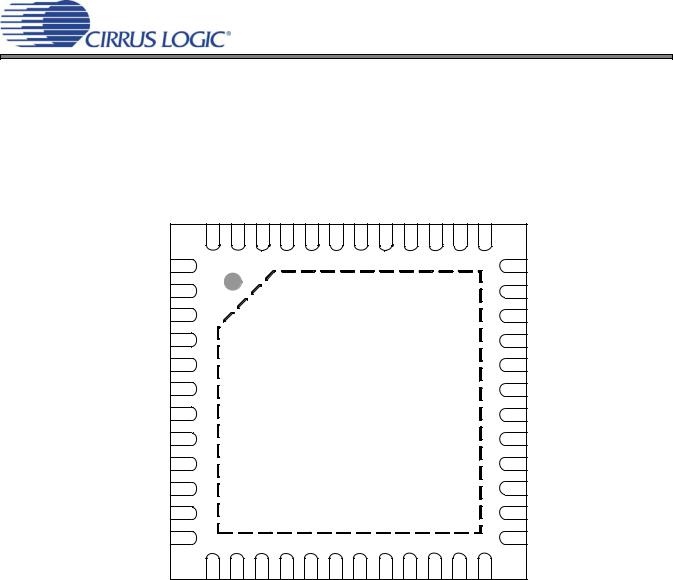
1. PIN DESCRIPTIONS
1.1 CS4207 48-pin QFN Pinout: |
|
|
|
|
|
|
|
|
|
|
||||
|
|
SPDIF OUT1 |
SPDIF IN |
VA HP |
FLYP |
VHP FILT+ |
FLYC |
FLYN |
VHP FILT- |
HPOUT R |
HPREF |
HPOUT L |
LINEOUT R1- |
|
|
|
48 |
47 |
46 |
45 |
44 |
43 |
42 |
41 |
40 |
39 |
38 |
37 |
|
VL_IF |
1 |
|
|
|
|
|
|
|
|
|
|
|
36 |
LINEOUT_R1+ |
GPIO0/DMIC_SDA1 |
2 |
|
|
|
|
|
|
|
|
|
|
|
35 |
LINEOUT_L1+ |
VL_HD |
3 |
|
|
|
|
|
|
|
|
|
|
|
34 |
LINEOUT_L1- |
DMIC_SCL |
4 |
|
|
|
|
|
|
|
|
|
|
|
33 |
LINEOUT_R2- |
SDO |
5 |
|
|
|
|
|
|
|
|
|
|
|
32 |
LINEOUT_R2+ |
BITCLK |
6 |
|
|
|
|
|
Thermal Pad |
|
|
|
31 |
LINEOUT_L2+ |
||
DGND |
|
|
|
|
|
|
|
|
|
|
LINEOUT_L2- |
|||
7 |
|
|
|
|
|
HPGND |
|
|
|
|
30 |
|||
SDI |
8 |
|
|
|
|
|
|
|
|
|
|
|
29 |
VBIAS (DAC) |
VD |
9 |
|
|
|
|
|
|
|
|
|
|
|
28 |
VCOM |
SYNC |
10 |
|
|
|
|
|
|
|
|
|
|
|
27 |
VREF+ (ADC) |
RESET# |
11 |
|
|
|
Top-Down (Through Package) View |
|
|
26 |
AGND |
|||||
|
|
|
|
|
|
48-Pin QFN Package |
|
|
|
|
VA |
|||
GPIO1/DMIC_SDA2 |
12 |
HPREF |
|
|
|
|
|
|
|
|
|
|
25 |
|
/SPDIF_OUT2 |
|
|
|
|
|
|
|
|
|
|
|
|
|
|
|
|
14 |
15 |
16 |
17 |
18 |
19 |
20 |
21 |
22 |
23 |
24 |
|
|
|
|
13 |
|
|||||||||||
|
|
SENSE A |
GPIO2 |
GPIO3 |
MICBIAS |
MICIN L- |
MICIN L+ |
MICIN R+ |
MICIN R- |
LINEIN L+ |
LINEIN C- |
LINEIN R+ |
VA REF |
|
Pin Name |
QFN |
Pin Description |
|
|
VL_IF |
1 |
Digital Interface Signal Level (Input) - Digital supply for the GPIO, S/PDIF and Digital Mic inter- |
|
|
faces. Refer to the Recommended Operating Conditions for appropriate voltages. |
||||
|
|
|||
|
|
|
||
GPIO0/ |
2 |
General Purpose I/O (Input/Output) - General purpose input or output line, or |
|
|
DMIC_SDA1 |
Digital Mic Data Input (Input) - The first data input line from a digital microphone. |
|||
|
||||
VL_HD |
3 |
Digital Interface Signal Level (Input) - Digital supply for the HD Audio interface. Refer to the |
|
|
Recommended Operating Conditions for appropriate voltages. |
||||
|
|
|||
DMIC_SCL |
4 |
Digital Mic Clock (Output) - The high speed clock output to the digital microphone. |
|
|
SDO |
5 |
Serial Data Input (Input) - Serial data input stream from the HD Audio Bus. |
|
|
|
|
|
||
BITCLK |
6 |
Bit Clock (Input) - 24 MHz bit clock from the HD Audio Bus. |
|
|
DGND |
7 |
Digital Ground (Input) - Ground reference for the internal digital section. |
|
|
SDI |
8 |
Serial Data Output (Input/Output) - Serial data output stream to the HD Audio Bus. |
|
|
|
|
|
||
VD |
9 |
Digital Power (Input) - Positive power for the internal digital section. |
|
|
SYNC |
10 |
Sync Clock (Input) - 48 kHz sync clock from the HD Audio Bus. |
|
|
|
|
|
|
|
8 |
|
DS880F4 |
||

|
|
|
CS4207 |
|
|
|
|
|
|
|
|
|
|
|
|
Pin Name |
QFN |
Pin Description |
|
|
|
|
|
|
|
RESET# |
11 |
Reset (Input) - The device enters a low power mode when this pin is driven low. |
|
|
|
|
|
|
|
GPIO1/ |
|
General Purpose I/O (Input/Output) - General purpose input or output line, or |
|
|
DMIC_SDA2/ |
12 |
Digital Mic Data Input (Input) - The second data input line from a digital microphone, or |
|
|
SPDIF_OUT2 |
|
S/PDIF Output (Output) - Output from internal S/PDIF Transmitter. |
|
|
SENSE_A |
13 |
Jack Sense Pin (Input/Output) - Jack sense detect. |
|
|
|
|
|
|
|
GPIO2 |
14 |
General Purpose I/O (Input/Output) - General purpose input or output lines. |
|
|
|
|
|
|
|
GPIO3 |
15 |
General Purpose I/O (Input/Output) - General purpose input or output lines. |
|
|
MICBIAS |
16 |
Microphone Bias (Output) - Provides a low noise bias supply for an external microphone. Elec- |
|
|
trical characteristics are specified in the DC Electrical Characteristics table. |
|||
|
|
|
||
|
|
|
|
|
|
MICIN_L- |
17 |
Microphone Input Left/Right (Input) - The full-scale level is specified in the ADC Analog Char- |
|
|
MICIN_L+ |
18 |
||
|
MICIN_R+ |
19 |
acteristics specification table. |
|
|
MICIN_R- |
20 |
|
|
|
|
|
|
|
|
LINEIN_L+ |
21 |
Analog Input (Input) - The full-scale level is specified in the ADC Analog Characteristics specifi- |
|
|
LINEIN_C- |
22 |
||
|
cation table. |
|||
|
LINEIN_R+ |
23 |
||
|
|
|
||
|
|
|
|
|
|
VA_REF |
24 |
Analog Power (Input) - Positive power for the internal analog section. VA_REF is the return pin |
|
|
VA |
25 |
for the VBIAS cap. |
|
|
|
|
|
|
|
AGND |
26 |
Analog Ground (Input) - Ground reference for the internal analog section. |
|
|
VREF+ |
27 |
Positive Voltage Reference (Output) - Positive reference voltage for the internal ADCs. |
|
|
|
|
|
|
|
VCOM |
28 |
Quiescent Voltage (Output) - Filter connection for internal quiescent voltage. |
|
|
|
|
|
|
|
VBIAS |
29 |
Positive Voltage Reference (Output) - Positive reference voltage for the internal DACs. |
|
|
LINEOUT_L2- |
30 |
|
|
|
LINEOUT_L2+ |
31 |
|
|
|
LINEOUT_R2+ |
32 |
Analog Audio Output (Output) - The full-scale output level is specified in the DAC Analog Char- |
|
|
LINEOUT_R2- |
33 |
||
|
LINEOUT_L1- |
34 |
acteristics specification table |
|
|
LINEOUT_L1+ |
35 |
|
|
|
LINEOUT_R1+ |
36 |
|
|
|
LINEOUT_R137 |
|
|
|
|
|
|
|
|
|
HPOUT_L |
38 |
Analog Headphone Output (Output) - The full-scale output level is specified in the DAC Analog |
|
|
HPOUT_R |
40 |
Characteristics specification table. |
|
|
|
|
|
|
|
HPREF |
39 |
Pseudo Diff. Headphone Reference (Input) - Ground reference for the headphone amplifiers. |
|
|
|
|
|
|
|
VHP_FILT- |
41 |
Inverting Charge Pump Filter Connection (Output) - Power supply from the inverting charge |
|
|
pump that provides the negative rail for the headphone amplifier. |
|||
|
|
|
||
|
|
|
|
|
|
FLYN |
42 |
Charge Pump Cap Negative Node (Output) - Negative node for the inverting charge pump’s fly- |
|
|
ing capacitor. |
|||
|
|
|
||
|
FLYC |
43 |
Charge Pump Cap Common Node (Output) - Common positive node for the step-down and |
|
|
inverting charge pumps’ flying capacitor. |
|||
|
|
|
||
|
|
|
|
|
|
VHP_FILT+ |
44 |
Non-Inverting Charge Pump Filter Connection (Output) - Power supply from the step-down |
|
|
charge pump that provides the positive rail for the headphone amplifier. |
|||
|
|
|
||
|
|
|
|
|
|
FLYP |
45 |
Charge Pump Cap Positive Node (Output) - Positive node for the step-down charge pump’s fly- |
|
|
ing capacitor. |
|||
|
|
|
||
|
VA_HP |
46 |
Analog Power For Headphone (Input) - Positive power for the internal analog headphone sec- |
|
|
tion. |
|||
|
|
|
||
|
|
|
|
|
|
SPDIF_IN |
47 |
S/PDIF Input (Input) - Input to internal S/PDIF Receiver. |
|
|
SPDIF_OUT1 |
48 |
S/PDIF Output (Output) - Output from internal S/PDIF Transmitter. |
|
|
HPGND |
TP |
HP Ground (Input) - Ground reference for the internal headphone section. See “QFN Thermal |
|
|
Pad” on page 144 for more information. |
|||
|
|
|
||
|
|
|
|
|
DS880F4 |
|
9 |
|
|

CS4207
1.2Digital I/O Pin Characteristics
Input and output levels and associated power supply voltage are shown in the table below. Logic levels should not exceed the corresponding power supply voltage.
Power |
Pin Name |
I/O |
Driver |
Receiver |
|
Supply |
SW/(HW) |
||||
|
|
|
|||
|
RESET# |
Input |
- |
1.5 V - 3.3 V |
|
|
SDO |
Input |
- |
1.5 V - 3.3 V |
|
VL_HD |
BITCLK |
Input |
- |
1.5 V - 3.3 V |
|
|
SDI (Note 1) |
Input/Output |
1.5 V - 3.3 V |
1.5 V - 3.3 V |
|
|
SYNC |
Input |
- |
1.5 V - 3.3 V |
|
VA |
SENSE_A |
Input |
- |
3.3 V - 5.0 V |
|
|
GPIO1/ |
Input/Output |
3.3 V |
3.3 V |
|
|
DMIC_SDA2 |
||||
|
|
|
|
||
|
GPIO2 |
Input/Output |
3.3 V |
3.3 V |
|
|
GPIO3 |
Input/Output |
3.3 V |
3.3 V |
|
VL_IF |
SPDIF_IN |
Input |
- |
3.3 V |
|
|
SPDIF_OUT |
Output |
3.3 V |
- |
|
|
GPIO0/ |
Input/Output |
3.3 V |
3.3 V |
|
|
DMIC_SDA1 |
||||
|
|
|
|
||
|
DMIC_SCL |
Output |
3.3 V |
- |
Notes:
1. SDI output functionality also requires the VA and VL_IF rails to be at nominal levels.
10 |
DS880F4 |
CS4207
2. TYPICAL CONNECTION DIAGRAMS
+5.0 V |
|
0.1 µF |
0.1 µF |
|
|
+1.8 V |
|
|
|
|
|
|
|
|
|
||
|
|
|
VA |
VD |
|
|
|
|
+5.0 V |
0.1 µF |
+ |
VA_REF |
|
|
|
|
|
|
10 µF |
|
|
|
|
Left Headphone |
||
|
|
|
|
HPOUT_L |
33 |
|
|
|
|
|
|
VBIAS |
0.1 µF |
|
|||
|
|
|
|
|
||||
+5.0 V |
|
|
CS4207 HPREF |
|
|
|
Headphone Ground |
|
|
|
VA_HP |
HPOUT_R |
|
|
|
Right Headphone |
|
|
|
|
VHP_FILT+ |
|
|
|
||
|
|
|
|
33 |
0.1 µF |
|
||
|
|
|
VHP_FILT- |
|
|
|||
|
** |
** |
|
|
|
|
|
|
|
|
|
|
|
|
|
||
|
0.1 µF 10 µF |
10 µF |
LINEOUT_L1+ |
|
|
Differential to |
‡ |
|
|
|
|
|
|
|
|||
|
|
|
|
LINEOUT_L1- |
|
|
Single-Ended |
+Left Line Output 1 |
|
** 2.2 µF |
FLYP |
|
|
Output Filter |
|
||
|
|
|
|
|
|
|
||
|
** 2.2 µF |
FLYC |
LINEOUT_R1+ |
|
|
Differential to |
‡ |
|
|
|
|
|
|||||
|
|
|
FLYN |
LINEOUT_R1- |
|
|
Single-Ended |
+Right Line Output 1 |
|
** Use low ESR |
|
|
Output Filter |
|
|||
ceramic capacitors.
|
|
|
|
|
|
|
|
|
|
|
LINEOUT_L2+ |
|
|
|
|
|
|
|
|
|
|
BITCLK |
LINEOUT_L2- |
|
|
|
|
|
|
|
|
|
|
||
|
|
|
|
|
|
|
|
|
|
|
|
HD Audio |
|
|
|
|
|
|
|
|
SYNC |
LINEOUT_R2+ |
|
|
|
|
|
|
|
|
|
||||
|
|
|
|
|
|
|
|
SDI |
|||
Bus |
|
|
|
|
|
|
|
|
LINEOUT_R2- |
||
|
|
|
|
|
|
|
|
SDO |
|||
|
|
|
|
|
|
|
|
|
|
||
|
|
|
|
|
|
|
|
|
|
||
|
|
|
|
|
|
|
|
|
|
RESET# |
|
|
|
|
|
|
|
|
|
|
|
|
|
|
+1.5 V to +3.3 V |
|
|
|
|
VL_HD |
|
||||
|
|
|
|
|
|
|
|
|
|
LINEIN_L+ |
|
|
|
|
|
|
|
|
|
|
|||
|
|
|
|
|
|
|
0.1 µF |
||||
|
|
|
|
|
|
|
|||||
|
|
|
|
|
|
|
|
|
|
|
LINEIN_C- |
|
|
|
|
|
|
|
|
|
|
|
|
+3.3 V |
|
|
|
|
|
|
|
|
VL_IF |
|||
|
|
|
|
|
|
|
||||||
|
|
|
|
|
|
|
|
0.1 µF |
||||
|
|
|
|
|
|
|
|
|||||
|
|
|
|
|
|
|
|
|
|
|
|
GPIO2 |
|
GPIO2 |
|
|
|
|
|||||||
|
||||||||||||
|
GPIO3 |
|
|
|
|
GPIO3 |
||||||
|
||||||||||||
|
*** SENSE_A |
|
|
|
|
|
SENSE_A |
|||||
|
|
|
|
|||||||||
|
S/PDIF RX |
|
|
|
|
|
|
SPDIF_IN |
||||
|
|
|
|
|||||||||
|
S/PDIF TX 1 |
|
|
|
|
SPDIF_OUT1 |
||||||
|
|
|
||||||||||
D-Mic In 2 / S/PDIF TX 2 |
|
|
|
|
DMIC_SDA2/ |
|||||||
|
|
|
|
SPDIF_OUT2 |
||||||||
|
|
|
|
|
|
|
|
|
|
|
|
|
|
D-Mic In 1 |
|
|
|
|
|
DMIC_SDA1 |
|||||
|
|
|
|
|||||||||
|
D-Mic Clk |
|
|
|
|
DMIC_SCL |
||||||
|
|
|
|
|
||||||||
*** See Figure 9. |
|
|
|
|
|
|||||||
|
|
|
|
|
|
|
|
|
|
|
|
HP_GND(Thermal |
LINEIN_R+ 


MICIN_L- 


MICIN_L+ 

MICBIAS
MICIN_R+ 


MICIN_R- 

VCOM
VREF+
AGND
Pad)
Differential to |
‡ |
|
Single-Ended |
+Left Line Output 2 |
|
Output Filter |
|
|
Differential to |
‡ |
|
Single-Ended |
+Right Line Output 2 |
|
Output Filter |
|
|
* Capacitors must be C0G or equivalent |
||
1 µF |
|
Left Analog Input |
* |
|
|
|
|
|
1800 pF |
|
|
1 µF |
|
|
1 µF |
|
Right Analog Input |
* |
|
|
|
|
|
1800 pF |
|
|
1 µF |
|
|
|
|
Differential Mic Left |
1 µF |
|
|
|
|
Microphone Bias |
|
RL |
The value of RL is dictated by |
0.47 µF |
|
the microphone cartridge. |
|
RL |
|
|
|
Differential Mic Right |
1 µF |
|
|
1 µF |
|
|
|
|
‡ Input and Output |
1 µF |
10 µF |
filters are optional. |
Figure 1. Typical Connection Diagram - Desktop System
DS880F4 |
11 |
CS4207
+3.3 V |
+1.8 V |
0.1 µF |
0.1 µF |
VA VD
+3.3 V |
+ |
VA_REF |
0.1 µF |
10 µF |
|
|
|
HPOUT_L |
|
|
VBIAS |
|
|
|
|
|
|
|
|
|
|
|
|
|
|
|
|
CS4207 HPREF |
|
+3.3 V |
|
|
|
|
|
|
|
|
|
|
|
VA_HP |
HPOUT_R |
||||
|
|
|
|
|
|
|
|
|
|
|
|
|
|||||
|
|
|
|
|
|
|
|
|
|
|
|
|
|
|
|
VHP_FILT+ |
|
|
|
|
|
|
|
|
|
|
|
|
|
|
|
|
|
|
|
0.1 µF |
** |
|
** |
|
|
|
|
|
|
|
VHP_FILT- |
|
|||||
|
|
|
|
|
|
|
|
|
|
||||||||
10 µF |
|
10 µF |
|
|
|
LINEOUT_L1+ |
|||||||||||
|
|
|
|
|
|
|
|
|
|
|
|
|
|
|
|
|
|
|
|
|
|
|
|
|
|
|
|
|
|
|
|
|
|
FLYP |
LINEOUT_L1- |
|
|
|
|
|
** 2.2 µF |
|
|
|
|
|
|
|
|||||
|
|
|
|
|
|
|
|
|
|
|
|
|
|||||
|
|
|
|
|
|
|
|
|
|
|
|
||||||
|
|
|
|
|
|
|
|
|
|
|
FLYC |
LINEOUT_R1+ |
|||||
|
|
|
|
|
|
||||||||||||
|
|
|
|
|
** 2.2 µF |
|
|
|
|
|
|
|
|||||
|
|
|
|
|
|
|
|
|
|
|
|||||||
|
|
|
|
|
|
|
|
|
|
|
FLYN |
LINEOUT_R1- |
|||||
|
|
|
|
|
|
|
|
|
|
|
|
|
|
|
|
||
|
|
|
|
|
|
|
|
|
|
|
|
|
|
|
|
||
|
|
|
* *Use low ESR |
|
|||||||||||||
|
ceramic capacitors. |
LINEOUT_L2+ |
|||||||||||||||
|
|
|
|
|
|
|
|
|
|
|
|
|
|
|
|
|
|
|
|
|
|
|
|
|
|
|
|
|
|
|
|
|
|
BITCLK |
LINEOUT_L2- |
|
|
|
|
|
|
|
|
|
|
|
|
|
|
|
|
||
|
|
|
|
|
|
|
|
|
|
|
|
|
|
||||
|
|
|
|
|
|
|
|
|
|
|
|
|
|
|
|
SYNC |
|
HD Audio |
|
|
|
|
|
|
|
|
|
|
|
|
|
|
|
|
|
|
|
|
|
|
|
|
|
|
|
|
|
|
|
||||
|
|
|
|
|
|
|
|
|
|
|
|
|
|
|
SDI |
|
|
Bus |
|
|
|
|
|
|
|
|
|
|
|
|
|
|
|
LINEOUT_R2+ |
|
|
|
|
|
|
|
|
|
|
|
|
|
|
|
|
SDO |
||
|
|
|
|
|
|
|
|
|
|
|
|
|
|
|
|
||
|
|
|
|
|
|
|
|
|
|
|
|
|
|
|
|
|
|
|
|
|
|
|
|
|
|
|
|
|
|
|
|
|
|
RESET# |
|
|
|
|
|
|
|
|
|
|
|
|
|
|
|
|
|||
|
|
|
|
|
|
|
|
|
|
|
|
|
|
|
|
|
|
LINEOUT_R2-
+1.5 V to +3.3 V
 VL_HD
VL_HD
33 |
Left Headphone |
0.1 µF |
 Headphone Ground
 Right Headphone
33 |
0.1 µF |
560 |
|
* |
2200 pF |
560 |
Speaker Driver |
560
 *2200 pF
560 Speaker Driver
|
|
|
|
|
|
|
0.1 µF |
|
|
* Capacitors must be C0G or equivalent |
|
|
|
|||||||
|
|
|
|
|
|
|
|
|
LINEIN_L+ |
|
|
|
|
|
|
1 µF |
|
|
Left Analog Input |
|
|
|
|
|
|
|
|
|
|
|
|
* |
|
|
|
|
|||||
|
|
|
|
|
|
|
|
|
|
|
|
|
|
|
|
|
|
|
|
|
|
|
|
|
|
|
|
|
|
|
|
|
|
|
|
1800 pF |
|
|
|
||
+3.3 V |
|
|
|
|
|
|
|
VL_IF |
LINEIN_C- |
|
|
|
|
|
|
1 µF |
|
|
|
|
|
|
|
|
|
|
|
|
|
|
|
|
|
|
|
|
|||||
|
|
|
|
|
|
|
0.1 µF |
LINEIN_R+ |
|
|
|
|
|
|
|
1 µF |
|
|
Right Analog Input |
|
|
|
|
|
|
|
|
|
|
|
|
|
|
|
|
|
|||||
|
|
|
|
|
|
|
|
|
|
|
|
|
|
|
|
|
|
|||
|
|
|
|
|
|
|
|
|
|
|
|
|
|
|
|
|
|
|||
|
|
|
|
|
|
|
|
|
|
|
|
|
* |
|
|
|
|
|
||
|
|
|
|
|
|
|
|
|
|
|
|
|
|
|
|
|
||||
|
|
|
|
|
|
|
|
|
|
|
|
|
|
1800 pF |
|
|
|
|||
GPIO2 
 GPIO2
GPIO2
GPIO3 
 GPIO3
GPIO3
*** SENSE_A  SENSE_A
S/PDIF RX  SPDIF_IN
S/PDIF TX 1 SPDIF_OUT1
D-Mic In 2 / S/PDIF TX 2 DMIC_SDA2/ SPDIF_OUT2
D-Mic In 1  DMIC_SDA1
D-Mic Clk  DMIC_SCL
MICIN_L- |
|
|
|
|
|
|
|
|||||||||
MICIN_L+ |
|
|
|
|
|
|
|
|
|
|
|
|
|
Left Mic In |
||
|
|
|
|
|
|
|
|
|
|
|
|
|
||||
|
|
|
|
|
|
1 µF |
|
|
|
|
|
|
|
|||
|
|
|
|
|
|
|
|
|
|
|
|
|
|
|
Microphone Bias |
|
MICBIAS |
|
|
|
|
|
|
|
|
|
|
|
|
|
|
||
|
|
|
|
|
|
|
|
|
RL |
|
|
The value of RL is dictated by |
|
|||
|
|
0.47 µF |
|
|
|
|
|
|
|
|
the microphone cartridge. |
|
||||
MICIN_R+ |
|
|
|
|
|
|
|
|
|
|
|
RL |
|
|
Right Mic In |
|
|
|
|
|
|
|
|
|
|
|
|
|
|
|
|||
|
|
|
|
|
|
|
|
|
|
|||||||
1 µF
MICIN_R-
|
VCOM |
*** See Figure 9. |
VREF+ |
|
1 µF 10 µF |
|
AGND |
|
HP_GND(Thermal Pad) |
|
Figure 2. Typical Connection Diagram - Portable System |
12 |
DS880F4 |

CS4207
3. CHARACTERISTICS AND SPECIFICATIONS
RECOMMENDED OPERATING CONDITIONS
(AGND=DGND=0 V, all voltages with respect to ground.) |
|
|
|
|
|
|
|
|
|
|
|
|
Units |
Parameters |
|
Symbol |
|
Min |
Max |
|
DC Power Supply (Note 1) |
|
|
|
|
|
|
Analog Core |
|
VA |
2.97 |
5.25 |
V |
|
DAC Reference |
|
VA_REF |
2.97 |
5.25 |
V |
|
Headphone Amplifier |
|
VA_HP |
2.97 |
5.25 |
V |
|
Digital Core |
|
VD |
1.42 |
1.89 |
V |
|
HD Audio Bus Interface |
|
VL_HD |
1.42 |
3.47 |
V |
|
GPIO, S/PDIF and Digital Mic Interface |
|
VL_IF |
2.97 |
3.47 |
V |
|
Ambient Temperature |
Commercial - CNZ |
TA |
-40 |
+85 |
C |
|
|
Automotive - DNZ |
-40 |
+105 |
C |
|
|
ABSOLUTE MAXIMUM RATINGS
(AGND = DGND = 0 V; all voltages with respect to ground.)
Parameters |
Symbol |
Min |
Max |
Units |
|
DC Power Supply |
Analog Core |
VA |
-0.3 |
5.5 |
V |
|
DAC Reference |
VA_REF |
-0.3 |
5.5 |
V |
|
Headphone Amplifier |
VA_HP |
-0.3 |
5.5 |
V |
|
Digital Core |
VD |
-0.3 |
3.0 |
V |
|
HD Audio Interface |
VL_HD |
-0.3 |
4.0 |
V |
GPIO, S/PDIF and Digital Mic Interface |
VL_IF |
-0.3 |
4.0 |
V |
|
Input Current |
(Note 2) |
Iin |
- |
±10 |
mA |
Analog Input Voltage |
(Note 3) |
VIN |
AGND-0.7 |
VA+0.7 |
V |
Digital Input Voltage |
(Note 3) HD Audio Interface |
VIND |
-0.3 |
VL_HD+0.4 |
V |
GPIO, S/PDIF and Digital Mic Interface |
|
-0.3 |
VL_IF+0.4 |
V |
|
Ambient Operating Temperature |
(power applied) |
TA |
-55 |
+115 |
°C |
Storage Temperature |
|
Tstg |
-65 |
+150 |
°C |
WARNING: Operation at or beyond these limits may result in permanent damage to the device. Normal operation is not guaranteed at these extremes.
Notes:
1.The device will operate properly over the full range of the analog, digital and interface supplies.
2.Any pin except supplies. Transient currents of up to ±100 mA on the analog input pins will not cause SCR latch-up.
3.The maximum over/under voltage is limited by the input current.
DS880F4 |
13 |

CS4207
ANALOG INPUT CHARACTERISTICS (COMMERCIAL - CNZ)
(Test Conditions (unless otherwise specified): Input sine wave (relative to digital full-scale): 1 kHz through passive input filter; VA_HP = VA; VL_HD = VL_IF = 3.3; VD = 1.8 V; TA = +25 C; Measurement Bandwidth is 10 Hz to
20 kHz unless otherwise specified. Sample Frequency = 48 kHz)
|
|
VA, VA_REF = 5.0 V |
VA, VA_REF = 3.3 V |
|
||||
Parameter (Note 4) |
|
(Differential/Single-ended) |
(Differential/Single-ended) |
|
||||
|
Min |
Typ |
Max |
Min |
Typ |
Max |
Unit |
|
Line In to PGA to ADC (ADC1 or ADC2; |
differential perf. characteristics |
only valid for ADC2) |
|
|||||
Dynamic Range |
|
|
|
|
|
|
|
|
PGA Setting: 0 dB |
A-weighted |
99/96 |
105/102 |
- |
95/93 |
101/99 |
- |
dB |
|
unweighted |
96/93 |
102/99 |
- |
92/90 |
98/96 |
- |
dB |
PGA Setting: +12 dB |
A-weighted |
95/86 |
101/92 |
- |
92/83 |
98/89 |
- |
dB |
|
unweighted |
92/83 |
98/89 |
- |
89/80 |
95/86 |
- |
dB |
Total Harmonic Distortion + Noise |
|
|
|
|
|
|
|
|
PGA Setting: 0 dB |
-1 dBFS |
- |
-88/-88 |
-82/-82 |
- |
-95/-92 |
-89/-86 |
dB |
|
-60 dBFS |
- |
-42/-39 |
-36/-33 |
- |
-38/-36 |
-32/-30 |
dB |
PGA Setting: +12 dB |
-1 dBFS |
- |
-88/-88 |
-82/-82 |
- |
-92/-86 |
-86/-80 |
dB |
Mic In to PGA to ADC (+20 dB) (ADC1 or |
ADC2; differential perf. characteristics only valid for ADC2) |
|||||||
Dynamic Range |
A-weighted |
86/78 |
92/84 |
- |
83/75 |
89/81 |
- |
dB |
|
||||||||
|
unweighted |
83/75 |
89/81 |
- |
80/72 |
86/78 |
- |
dB |
Total Harmonic Distortion + Noise |
|
|
|
|
|
|
|
|
|
-1 dBFS |
- |
-89/-82 |
-83/-76 |
- |
-86/-78 |
-80/-72 |
dB |
Other Analog Characteristics |
|
|
|
|
|
|
|
|
DC Accuracy |
|
|
|
|
|
|
|
|
Interchannel Gain Mismatch |
- |
0.2 |
- |
- |
0.2 |
- |
dB |
|
Gain Drift |
|
- |
±100 |
- |
- |
±100 |
- |
ppm/°C |
Offset Error |
High Pass Filter On |
- |
352 |
- |
- |
352 |
- |
LSB |
Interchannel Isolation |
|
- |
90 |
- |
- |
90 |
- |
dB |
HP Amp to Analog Input Isolation |
|
|
|
|
|
|
|
|
|
RL = 10 k |
- |
100 |
- |
- |
100 |
- |
dB |
|
RL = 16 |
- |
70 |
- |
- |
70 |
- |
dB |
Full-scale Input Voltage - Line In/Mic In |
1.58•VA |
1.66•VA |
1.74•VA |
1.58•VA |
1.66•VA |
1.74•VA |
Vpp |
|
(Differential Inputs) |
PGA(0dB) |
|||||||
Full-scale Input Voltage - Line In PGA (0dB) |
0.79•VA |
0.83•VA |
0.87•VA |
0.79•VA |
0.83•VA |
0.87•VA |
Vpp |
|
(Single-ended Inputs) |
PGA (+12dB) |
|
0.21•VA |
|
|
0.21•VA |
|
Vpp |
|
|
|
|
|
|
|||
Full-scale Input Voltage - Mic In |
0.79•VA |
0.83•VA |
0.87•VA |
0.79•VA |
0.83•VA |
0.87•VA |
Vpp |
|
|
PGA+Boost(0dB) |
|||||||
(Single-ended Inputs) |
PGA+Boost(+20dB) |
|
0.08•VA |
|
|
0.08•VA |
|
Vpp |
Input Impedance (Note 5) |
|
- |
43.5 |
- |
- |
43.5 |
- |
k |
Mic In (Differential or Pseudo-Diff) |
||||||||
Line In (Pseudo-Diff, PGA = -12/0/+12 dB) |
- |
93/99/103 |
- |
- |
93/99/103 |
- |
k |
|
Mic/Line In (Single-Ended, PGA = -12/0/+12 dB) |
- |
27/33/37 |
- |
- |
27/33/37 |
- |
k |
|
Common Mode Rejection (Differential Inputs) |
- |
60 |
- |
- |
60 |
- |
dB |
|
14 |
DS880F4 |

CS4207
ANALOG INPUT CHARACTERISTICS (AUTOMOTIVE - DNZ)
(Test Conditions (unless otherwise specified): Input sine wave (relative to digital full-scale): 1 kHz through passive input filter; VA_HP = VA; VL_HD = VL_IF = 3.3; VD = 1.8 V; TA = -40 to +85 C; Measurement Bandwidth is 10 Hz
to 20 kHz unless otherwise specified. Sample Frequency = 48 kHz)
|
|
VA, VA_REF = 5.0 V |
VA, VA_REF = 3.3 V |
|
||||
Parameter (Note 4) |
|
(Differential/Single-ended) |
(Differential/Single-ended) |
|
||||
|
Min |
Typ |
Max |
Min |
Typ |
Max |
Unit |
|
Line In to PGA to ADC (ADC1 or ADC2; differential perf. characteristics only valid for ADC2) |
|
|
||||||
Dynamic Range |
|
|
|
|
|
|
|
|
PGA Setting: 0 dB |
A-weighted |
99/96 |
105/102 |
- |
95/93 |
101/99 |
- |
dB |
|
unweighted |
96/93 |
102/99 |
- |
92/90 |
98/96 |
- |
dB |
PGA Setting: +12 dB |
A-weighted |
95/86 |
101/92 |
- |
92/83 |
98/89 |
- |
dB |
|
unweighted |
92/83 |
98/89 |
- |
89/80 |
95/86 |
- |
dB |
Total Harmonic Distortion + Noise |
|
|
|
|
|
|
|
|
PGA Setting: 0 dB |
-1 dBFS |
- |
-88/-88 |
-82/-82 |
- |
-95/-92 |
-89/-86 |
dB |
|
-60 dBFS |
- |
-42/-39 |
-36/-33 |
- |
-38/-36 |
-32/-30 |
dB |
PGA Setting: +12 dB |
-1 dBFS |
- |
-88/-88 -82/-82 |
- |
-92/-86 |
-86/-80 |
dB |
|
Mic In to PGA to ADC (+20 dB) (ADC1 or ADC2; differential perf. characteristics only valid for ADC2) |
|
|||||||
Dynamic Range |
A-weighted |
86/78 |
92/84 |
- |
83/75 |
89/81 |
- |
dB |
|
||||||||
|
unweighted |
83/75 |
89/81 |
- |
80/72 |
86/78 |
- |
dB |
Total Harmonic Distortion + Noise |
|
|
|
|
|
|
|
|
|
-1 dBFS |
- |
-89/-82 |
-83/-76 |
- |
-86/-78 |
-80/-72 |
dB |
Other Analog Characteristics |
|
|
|
|
|
|
|
|
DC Accuracy |
|
|
|
|
|
|
|
|
Interchannel Gain Mismatch |
- |
0.2 |
- |
- |
0.2 |
- |
dB |
|
Gain Drift |
|
- |
±100 |
- |
- |
±100 |
- |
ppm/°C |
Offset Error |
High Pass Filter On |
- |
352 |
- |
- |
352 |
- |
LSB |
Interchannel Isolation |
|
- |
90 |
- |
- |
90 |
- |
dB |
HP Amp to Analog Input Isolation |
|
|
|
|
|
|
|
|
|
RL = 10 k |
- |
100 |
- |
- |
100 |
- |
dB |
|
RL = 16 |
- |
70 |
- |
- |
70 |
- |
dB |
Full-scale Input Voltage - Line In/Mic In |
1.58•VA |
1.66•VA |
1.74•VA |
1.58•VA |
1.66•VA |
1.74•VA |
Vpp |
|
(Differential Inputs) |
PGA(0dB) |
|||||||
Full-scale Input Voltage - Line In PGA(0dB) |
0.79•VA |
0.83•VA |
0.87•VA |
0.79•VA |
0.83•VA |
0.87•VA |
Vpp |
|
(Single-ended Inputs) |
PGA(+12dB) |
|
0.21•VA |
|
|
0.21•VA |
|
Vpp |
|
|
|
|
|
|
|||
Full-scale Input Voltage - Mic In |
0.79•VA |
0.83•VA |
0.87•VA |
0.79•VA |
0.83•VA |
0.87•VA |
Vpp |
|
|
PGA+Boost(0dB) |
|||||||
(Single-ended Inputs) |
PGA+Boost(+20dB) |
|
0.08•VA |
|
|
0.08•VA |
|
Vpp |
Input Impedance (Note 5) |
|
- |
|
- |
- |
|
- |
k |
Mic In (Differential or Pseudo-Diff) |
|
43.5 |
|
|
43.5 |
|
||
Line In (Pseudo-Diff, PGA = -12/0/+12 dB) |
|
93/99/103 |
|
|
93/99/103 |
|
k |
|
Mic/Line In (Single-Ended, PGA = -12/0/+12 dB) |
|
27/33/37 |
|
|
27/33/37 |
|
k |
|
Common Mode Rejection (Differential Inputs) |
- |
60 |
- |
- |
60 |
- |
dB |
|
4.Referred to the typical full-scale voltage. Applies to all THD+N and Dynamic Range values in the table.
5.Measured between [LINE/MIC]IN_[L/R]+ and [LINE/MIC]IN_[C/L/R]- for differential and pseudo-differ- ential inputs, and between [LINE/MIC]IN_[L/R]+ and AGND for single-ended inputs.
DS880F4 |
15 |

CS4207
ADC DIGITAL FILTER CHARACTERISTICS
|
Parameter (Note 6) |
|
Min |
Typ |
Max |
Unit |
Passband (Frequency Response) |
to -0.1 dB corner |
0 |
- |
.4535 |
Fs |
|
Passband Ripple |
|
|
-0.09 |
- |
0.17 |
dB |
Stopband |
|
|
0.6 |
- |
- |
Fs |
Stopband Attenuation |
|
|
70 |
- |
- |
dB |
Total Group Delay |
|
|
- |
7.6/Fs |
- |
s |
High-Pass Filter Characteristics (48 kHz Fs) |
|
|
|
|
|
|
Frequency Response |
-3.0 dB |
|
- |
3.6 |
- |
Hz |
|
-0.13 dB |
|
- |
24.2 |
- |
Hz |
Phase Deviation |
@ 20 Hz |
|
- |
10 |
- |
Deg |
Passband Ripple |
|
|
- |
- |
0.17 |
dB |
Filter Settling Time |
|
|
- |
105/Fs |
0 |
s |
6. Response is clock dependent and will scale with Fs.
16 |
DS880F4 |

CS4207
ANALOG OUTPUT CHARACTERISTICS (COMMERCIAL - CNZ)
(Test conditions (unless otherwise specified): Input test signal is a full-scale 997 Hz sine wave; VD = 1.8 V; VL_HD = VL_IF = 3.3V; TA = +25 C; Measurement bandwidth is 10 Hz to 20 kHz; test load RL = 10 k CL = 10 pF
for the line output and test load RL = 16 CL = 10 pF for the headphone output (see Figure 3); DAC Gain = 0 dB).
|
|
|
VA, VA_REF = 5.0 V |
VA, VA_REF = 3.3 V |
|
|
||||
|
|
|
VA_HP = 5.0 V |
VA_HP = 3.3 V |
|
|
||||
|
|
|
(Single-ended) |
(Single-ended) |
|
|
||||
Parameter (Note 4) |
|
|
Min |
Typ |
Max |
Min |
Typ |
Max |
Unit |
|
DAC1; RL = 16 ; DAC Gain = -5 dB |
|
|
|
|
|
|
|
|
||
Dynamic Range |
|
|
|
|
|
|
|
|
|
|
18 to 24-Bit |
A-weighted |
95 |
101 |
- |
93 |
99 |
- |
dB |
|
|
|
unweighted |
92 |
98 |
- |
90 |
96 |
- |
dB |
|
|
16-Bit |
A-weighted |
- |
93 |
- |
- |
93 |
- |
dB |
|
|
|
unweighted |
- |
90 |
- |
- |
90 |
- |
dB |
|
|
Total Harmonic Distortion + Noise |
|
|
|
|
|
|
|
|
||
18 to 24-Bit |
|
0 dB |
- |
-89 |
-83 |
- |
-93 |
-87 |
dB |
|
|
|
-20 dB |
- |
-78 |
-72 |
- |
-76 |
-70 |
dB |
|
|
|
-60 dB |
- |
-38 |
-32 |
- |
-36 |
-30 |
dB |
|
16-Bit |
|
0 dB |
- |
-89 |
- |
- |
-90 |
- |
dB |
|
|
|
-20 dB |
- |
-70 |
- |
- |
-70 |
- |
dB |
|
|
|
-60 dB |
- |
-30 |
- |
- |
-30 |
- |
dB |
|
DAC1; RL = 10 k |
|
|
|
|
|
|
|
|
|
|
Dynamic Range |
|
|
|
|
|
|
|
|
|
|
18 to 24-Bit |
A-weighted |
100 |
106 |
- |
98 |
104 |
- |
dB |
|
|
|
unweighted |
97 |
103 |
- |
95 |
101 |
- |
dB |
|
|
16-Bit |
A-weighted |
- |
96 |
- |
- |
96 |
- |
dB |
|
|
|
unweighted |
- |
93 |
- |
- |
93 |
- |
dB |
|
|
Total Harmonic Distortion + Noise |
|
|
|
|
|
|
|
|
||
18 to 24-Bit |
|
0 dB |
- |
-88 |
-82 |
- |
-90 |
-84 |
dB |
|
|
|
-20 dB |
- |
-83 |
-77 |
- |
-81 |
-75 |
dB |
|
|
|
-60 dB |
- |
-43 |
-37 |
- |
-41 |
-35 |
dB |
|
16-Bit |
|
0 dB |
- |
-88 |
- |
- |
-90 |
- |
dB |
|
|
|
-20 dB |
- |
-73 |
- |
- |
-73 |
- |
dB |
|
|
|
-60 dB |
- |
-33 |
- |
- |
-33 |
- |
dB |
|
Other Characteristics for DAC1; RL = 16 or 10 k |
|
|
|
|
|
|
||||
Full-scale Output Voltage, RL = 10 k |
0.80•VA |
0.84•VA |
0.88•VA |
0.80•VA |
0.84•VA |
0.88•VA |
Vpp |
|
||
Output Power, THD+N = -75 dB, RL = 16 |
- |
38 |
- |
- |
17 |
- |
mW |
|
||
|
|
|
|
|
|
|
|
|
rms |
|
Output Power, THD+N = 1%, RL = 16 |
- |
50 |
- |
- |
23 |
- |
mWrms |
|
||
Output Power,THD+N = 10%, RL = 16 |
- |
74 |
- |
- |
35 |
- |
mWrms |
|
||
Interchannel Isolation (1 kHz) |
16 |
- |
80 |
- |
- |
80 |
- |
dB |
|
|
|
|
10 k |
- |
95 |
- |
- |
93 |
- |
dB |
|
Interchannel Gain Mismatch |
|
|
- |
0.1 |
0.25 |
- |
0.1 |
0.25 |
dB |
|
Output Offset Voltage DAC to HPOUT |
- |
2 |
4 |
- |
2 |
4 |
mV |
|
||
Gain Drift |
|
|
- |
±100 |
- |
- |
±100 |
- |
ppm/°C |
|
AC-Load Resistance (RL) |
|
(Note 7) |
16 |
- |
- |
16 |
- |
- |
|
|
Load Capacitance (CL) |
|
(Note 7) |
- |
- |
150 |
- |
- |
150 |
pF |
|
Output Impedance |
|
|
- |
300 |
- |
- |
300 |
- |
m |
|
|
|
|
|
|
|
|
|
|
|
|
DS880F4 |
|
|
|
|
|
|
|
|
17 |
|

|
|
|
|
|
|
|
CS4207 |
|
|
|
|
|
|
|
|
||||
|
|
|
|
|
|
||||
|
|
VA, VA_REF = 5.0 V |
VA, VA_REF = 3.3 V |
|
|
||||
|
|
(Differential/Single-ended) |
(Differential/Single-ended) |
|
|
||||
Parameter (Note 4) |
|
Min |
Typ |
Max |
Min |
Typ |
Max |
Unit |
|
DAC2/DAC3; RL = 10 k |
|
|
|
|
|
|
|
|
|
Dynamic Range |
|
|
|
|
|
|
|
|
|
18 to 24-Bit |
A-weighted |
104/100 |
110/106 |
- |
101/97 |
107/103 |
- |
dB |
|
|
unweighted |
101/97 |
107/103 |
- |
98/94 |
104/100 |
- |
dB |
|
16-Bit |
A-weighted |
- |
96 |
- |
- |
96 |
- |
dB |
|
|
unweighted |
- |
93 |
- |
- |
93 |
- |
dB |
|
Total Harmonic Distortion + Noise |
|
|
|
|
|
|
|
|
|
18 to 24-Bit |
0 dB |
- |
-94/-91 |
-88/-85 |
- |
-96/-94 |
-90/-88 |
dB |
|
|
-20 dB |
- |
-87/-83 |
-81/-77 |
- |
-84/-80 |
-78/-74 |
dB |
|
|
-60 dB |
- |
-47/-43 |
-41/-37 |
- |
-44/-40 |
-38/-34 |
dB |
|
16-Bit |
0 dB |
- |
-92 |
- |
- |
-92 |
- |
dB |
|
|
-20 dB |
- |
-73 |
- |
- |
-73 |
- |
dB |
|
|
-60 dB |
- |
-33 |
- |
- |
-33 |
- |
dB |
|
Other Characteristics for DAC2/DAC3; |
RL = 10 k |
|
|
|
|
|
|
||
Full-scale Output Voltage |
|
1.60•VA/ |
1.68•VA/ |
1.76•VA/ |
1.60•VA/ |
1.68•VA/ |
1.76•VA/ |
Vpp |
|
|
0.80•VA |
0.84•VA |
0.88•VA |
0.80•VA |
0.84•VA |
0.88•VA |
|
|
|
|
|
|
|
||||||
Interchannel Isolation (1 kHz) |
- |
100 |
- |
- |
100 |
- |
dB |
|
|
Interchannel Gain Mismatch |
|
- |
0.1 |
0.25 |
- |
0.1 |
0.25 |
dB |
|
Gain Drift |
|
- |
±100 |
- |
- |
±100 |
- |
ppm/°C |
|
AC-Load Resistance (RL) |
(Note 7) |
3 |
- |
- |
3 |
- |
- |
k |
|
Load Capacitance (CL) |
(Note 7) |
- |
- |
100 |
- |
- |
100 |
pF |
|
Output Impedance |
|
- |
100 |
- |
- |
100 |
- |
|
|
7.See Figure 3 and Figure 4. RL and CL reflect the recommended minimum resistance and maximum capacitance required for the internal op-amp's stability and signal integrity.
HPOUT_L/R |
|
LINEOUT_L/R |
|
33 |
|
|
|
|
|
|
|
C L |
R L |
C L |
R L |
|
|
||
0.1 F |
|
|
|
AGND |
|
AGND |
|
|
|
|
Figure 3. Output Test Load, Headphone Out Figure 4. Output Test Load, Line Out
18 |
DS880F4 |

CS4207
ANALOG OUTPUT CHARACTERISTICS (AUTOMOTIVE - DNZ)
(Test conditions (unless otherwise specified): Input test signal is a full-scale 997 Hz sine wave; VD = 1.8 V; VL_HD = VL_IF = 3.3V; TA = -40 to +85 C; Measurement bandwidth is 10 Hz to 20 kHz; test load RL = 10 k CL = 10 pF
for the line output and test load RL = 16 CL = 10 pF for the headphone output (see Figure 5); DAC Gain = 0 dB).
|
|
|
VA, VA_REF = 5.0 V |
VA, VA_REF = 3.3 V |
|
|
||||
|
|
|
VA_HP = 5.0 V |
VA_HP = 3.3 V |
|
|
||||
|
|
|
(Single-ended) |
(Single-ended) |
|
|
||||
Parameter (Note 4) |
|
|
Min |
Typ |
Max |
Min |
Typ |
Max |
Unit |
|
DAC1; RL = 16 ; DAC Gain = -5 dB |
|
|
|
|
|
|
|
|
||
Dynamic Range |
|
|
|
|
|
|
|
|
|
|
18 to 24-Bit |
A-weighted |
95 |
101 |
- |
93 |
99 |
- |
dB |
|
|
|
unweighted |
92 |
98 |
- |
90 |
96 |
- |
dB |
|
|
16-Bit |
A-weighted |
- |
93 |
- |
- |
93 |
- |
dB |
|
|
|
unweighted |
- |
90 |
- |
- |
90 |
- |
dB |
|
|
Total Harmonic Distortion + Noise |
|
|
|
|
|
|
|
|
||
18 to 24-Bit |
|
0 dB |
- |
-89 |
-83 |
- |
-93 |
-87 |
dB |
|
|
|
-20 dB |
- |
-78 |
-72 |
- |
-76 |
-70 |
dB |
|
|
|
-60 dB |
- |
-38 |
-32 |
- |
-36 |
-30 |
dB |
|
16-Bit |
|
0 dB |
- |
-89 |
- |
- |
-90 |
- |
dB |
|
|
|
-20 dB |
- |
-70 |
- |
- |
-70 |
- |
dB |
|
|
|
-60 dB |
- |
-30 |
- |
- |
-30 |
- |
dB |
|
DAC1; RL = 10 k |
|
|
|
|
|
|
|
|
|
|
Dynamic Range |
|
|
|
|
|
|
|
|
|
|
18 to 24-Bit |
A-weighted |
100 |
106 |
- |
98 |
104 |
- |
dB |
|
|
|
unweighted |
97 |
103 |
- |
95 |
101 |
- |
dB |
|
|
16-Bit |
A-weighted |
- |
96 |
- |
- |
96 |
- |
dB |
|
|
|
unweighted |
- |
93 |
- |
- |
93 |
- |
dB |
|
|
Total Harmonic Distortion + Noise |
|
|
|
|
|
|
|
|
||
18 to 24-Bit |
|
0 dB |
- |
-88 |
-82 |
- |
-90 |
-84 |
dB |
|
|
|
-20 dB |
- |
-83 |
-77 |
- |
-81 |
-75 |
dB |
|
|
|
-60 dB |
- |
-43 |
-37 |
- |
-41 |
-35 |
dB |
|
16-Bit |
|
0 dB |
- |
-88 |
- |
- |
-90 |
- |
dB |
|
|
|
-20 dB |
- |
-73 |
- |
- |
-73 |
- |
dB |
|
|
|
-60 dB |
- |
-33 |
- |
- |
-33 |
- |
dB |
|
Other Characteristics for DAC1; RL = 16 or 10 k |
|
|
|
|
|
|
||||
Full-scale Output Voltage, RL = 10 k |
0.80•VA |
0.84•VA |
0.88•VA |
0.80•VA |
0.84•VA |
0.88•VA |
Vpp |
|
||
Output Power, THD+N = -75 dB, RL = 16 |
- |
38 |
- |
- |
17 |
- |
mW |
|
||
|
|
|
|
|
|
|
|
|
rms |
|
Output Power, THD+N = 1%, RL = 16 |
- |
50 |
- |
- |
23 |
- |
mWrms |
|
||
Output Power,THD+N = 10%, RL = 16 |
- |
74 |
- |
- |
35 |
- |
mWrms |
|
||
Interchannel Isolation (1 kHz) |
16 |
- |
80 |
- |
- |
80 |
- |
dB |
|
|
|
|
10 k |
- |
95 |
- |
- |
93 |
- |
dB |
|
Interchannel Gain Mismatch |
|
|
- |
0.1 |
0.25 |
- |
0.1 |
0.25 |
dB |
|
Output Offset Voltage DAC to HPOUT |
- |
2 |
5 |
- |
2 |
5 |
mV |
|
||
Gain Drift |
|
|
- |
±100 |
- |
- |
±100 |
- |
ppm/°C |
|
AC-Load Resistance (RL) |
|
(Note 8) |
16 |
- |
- |
16 |
- |
- |
|
|
Load Capacitance (CL) |
|
(Note 8) |
- |
- |
150 |
- |
- |
150 |
pF |
|
Output Impedance |
|
|
- |
300 |
- |
- |
300 |
- |
m |
|
|
|
|
|
|
|
|
|
|
|
|
DS880F4 |
|
|
|
|
|
|
|
|
19 |
|
|
|
|
|
|
|
|
CS4207 |
|
|
|
|
|
|
|
|
||||
|
|
|
|
|
|
||||
|
|
VA, VA_REF = 5.0 V |
VA, VA_REF = 3.3 V |
|
|
||||
|
|
(Differential/Single-ended) |
(Differential/Single-ended) |
|
|
||||
Parameter (Note 4) |
|
Min |
Typ |
Max |
Min |
Typ |
Max |
Unit |
|
DAC2/DAC3; RL = 10 k |
|
|
|
|
|
|
|
|
|
Dynamic Range |
|
|
|
|
|
|
|
|
|
18 to 24-Bit |
A-weighted |
104/100 |
110/106 |
- |
101/97 |
107/103 |
- |
dB |
|
|
unweighted |
101/97 |
107/103 |
- |
98/94 |
104/100 |
- |
dB |
|
16-Bit |
A-weighted |
- |
96 |
- |
- |
96 |
- |
dB |
|
|
unweighted |
- |
93 |
- |
- |
93 |
- |
dB |
|
Total Harmonic Distortion + Noise |
|
|
|
|
|
|
|
|
|
18 to 24-Bit |
0 dB |
- |
-94/-91 |
-88/-85 |
- |
-96/-94 |
-88/-88 |
dB |
|
|
-20 dB |
- |
-87/-83 |
-81/-77 |
- |
-84/-80 |
-78/-74 |
dB |
|
|
-60 dB |
- |
-47/-43 |
-41/-37 |
- |
-44/-40 |
-38/-34 |
dB |
|
16-Bit |
0 dB |
- |
-92 |
- |
- |
-92 |
- |
dB |
|
|
-20 dB |
- |
-73 |
- |
- |
-73 |
- |
dB |
|
|
-60 dB |
- |
-33 |
- |
- |
-33 |
- |
dB |
|
Other Characteristics for DAC2/DAC3; |
RL = 10 k |
|
|
|
|
|
|
||
Full-scale Output Voltage |
|
1.60•VA/ |
1.68•VA/ |
1.76•VA/ |
1.60•VA/ |
1.68•VA/ |
1.76•VA/ |
Vpp |
|
|
0.80•VA |
0.84•VA |
0.88•VA |
0.80•VA |
0.84•VA |
0.88•VA |
|
|
|
|
|
|
|
||||||
Interchannel Isolation (1 kHz) |
- |
100 |
- |
- |
100 |
- |
dB |
|
|
Interchannel Gain Mismatch |
|
- |
0.1 |
0.25 |
- |
0.1 |
0.25 |
dB |
|
Gain Drift |
|
- |
±100 |
- |
- |
±100 |
- |
ppm/°C |
|
AC-Load Resistance (RL) |
(Note 8) |
3 |
- |
- |
3 |
- |
- |
k |
|
Load Capacitance (CL) |
(Note 8) |
- |
- |
100 |
- |
- |
100 |
pF |
|
Output Impedance |
|
- |
100 |
- |
- |
100 |
- |
|
|
8.See Figure 5 and Figure 6. RL and CL reflect the recommended minimum resistance and maximum capacitance required for the internal op-amp's stability and signal integrity.
HPOUT_L/R |
|
LINEOUT_L/R |
|
33 |
|
|
|
C L |
R L |
C L |
R L |
0.1 F |
|
|
|
AGND |
|
AGND |
|
Figure 5. Output Test Load, Headphone Out Figure 6. Output Test Load, Line Out
20 |
DS880F4 |
CS4207
COMBINED DAC INTERPOLATION & ON-CHIP ANALOG FILTER RESPONSE
Parameter |
|
Min |
Typ |
Max |
Unit |
|
|
|
|
|
|
Frequency Response 10 Hz to 20 kHz |
|
-0.01 |
- |
+0.01 |
dB |
|
|
|
|
|
|
Passband |
to -0.01 dB corner |
0 |
- |
21792 |
Hz |
|
to -3 dB corner |
0 |
- |
23952 |
Hz |
|
|
|
|
|
|
StopBand |
|
- |
26256 |
- |
Hz |
|
|
|
|
|
|
StopBand Attenuation (Note 9) |
|
- |
102 |
- |
dB |
|
|
|
|
|
|
Total Group Delay |
|
- |
0.196 |
- |
ms |
|
|
|
|
|
|
9. Measurement Bandwidth is from Stopband to 100 kHz.
DC ELECTRICAL CHARACTERISTICS
(AGND = 0 V; all voltages with respect to ground.)
Parameters |
|
Min |
Typ |
Max |
Units |
|
|
|
|
|
|
VCOM Characteristics |
|
|
|
|
|
Nominal Voltage |
|
- |
0.5•VA |
- |
V |
Output Impedance |
|
- |
23 |
- |
k |
DC Current Source/Sink (Note 10) |
|
- |
- |
10 |
A |
|
|
|
|
|
|
VHP_FILT+ Characteristics |
|
|
|
|
|
Nominal Voltage |
|
- |
0.5•VA_HP |
- |
V |
|
|
|
|
|
|
VHP_FILTCharacteristics |
|
|
|
|
|
Nominal Voltage |
|
- |
-0.5•VA_HP |
- |
V |
|
|
|
|
|
|
MIC BIAS Characteristics |
|
|
|
|
|
Nominal Voltage |
VREFE = 000b |
- |
Hi-Z |
- |
V |
|
VREFE = 001b |
- |
0.5•VA |
- |
V |
|
VREFE = 010b |
- |
GND |
- |
V |
|
VREFE = 100b |
- |
0.8•VA |
- |
V |
DC Current Source |
(VA=5.0V) |
- |
5 |
- |
mA |
|
(VA=3.3V) |
- |
3 |
- |
mA |
|
|
|
|
|
|
Power Supply Rejection Ratio (PSRR) (Note 11) |
1 kHz |
- |
60 |
- |
dB |
|
|
|
|
|
|
10.The DC current draw represents the allowed current draw from the VCOM pin due to typical leakage through electrolytic de-coupling capacitors.
11.Valid with the recommended capacitor values on VBIAS. Increasing the capacitance will also increase the PSRR.
DS880F4 |
21 |
CS4207
DIGITAL MICROPHONE INTERFACE CHARACTERISTICS
Test conditions: Inputs: Logic 0 = GND = 0 V, Logic 1 = VL_IF; TA = +25 C; CLOAD = 30 pF.
Parameters |
|
Symbol |
Min |
Typ |
Max |
Units |
|
|
|
|
|
|
|
DMIC_SCL Period (FsADC >= 44.1 kHz) |
(Note 12) |
tP |
- |
8 • T_cyc |
- |
ns |
DMIC_SCL Period (FsADC <= 32.0 kHz) |
(Note 12) |
tP |
- |
12 • T_cyc |
- |
ns |
DMIC_SCL Duty Cycle |
|
- |
45 |
- |
55 |
% |
|
|
|
|
|
|
|
DMIC_SCL Rise Time |
(Note 13) |
tr |
- |
- |
10 |
ns |
DMIC_SCL Fall Time |
(Note 13) |
tf |
- |
- |
10 |
ns |
DMIC_SDA Setup Time Before DMIC_SCL Rising Edge |
ts(SD-CLKR) |
40 |
- |
- |
ns |
|
DMIC_SDA Hold Time After DMIC_SCL Rising Edge |
|
th(CLKR-SD) |
5 |
- |
- |
ns |
DMIC_SDA Setup Time Before DMIC_SCL Falling Edge |
ts(SD-CLKF) |
40 |
- |
- |
ns |
|
DMIC_SDA Hold Time After DMIC_SCL Falling Edge |
th(CLKF-SD) |
6 |
- |
- |
ns |
|
Notes:
12.The output clock frequency will follow the Bit Clock (BITCLK) frequency divided by 8 or 12, depending on the sample rate of the ADC. Any deviation of the Bit Clock source from the nominal supported rates will be directly imparted to the output clock rate by the same factor (e.g. +100 ppm offset in the frequency of BITCLK will become a +100 ppm offset in DMIC_SCL). For the nominal value of T_cyc reference HDA024-A (see Note 4 in “References” on page 147).
13.Rise and fall times are measured from 0.1 • VL_IF to 0.9 • VL_IF.
DMIC_SCL
DMIC_SDA
|
tP |
|
|
|
tf |
|
tr |
|
ts(SD-CLKF) |
ts(SD-CLKR) |
|
Left |
Right |
|
Left |
(A, DATA1) |
(B, DATA2) |
|
(A, DATA1) |
Channel Data |
Channel Data |
|
Channel Data |
|
th(CLKF-SD) |
th(CLKR-SD) |
|
Figure 7. Digital MIC Interface Timing
22 |
DS880F4 |

CS4207
DIGITAL INTERFACE SPECIFICATIONS & CHARACTERISTICS
Parameters (Note 14) |
Symbol |
Min |
Max |
Units |
|
Input Leakage Current |
Iin |
- |
±10 |
A |
|
Input Pin Capacitance |
Cin |
- |
7.5 |
pF |
|
VL_HD = 1.5 V |
|
|
|
|
|
High-Level Input Voltage |
VIH |
0.60•VL_HD |
- |
V |
|
Low-Level Input Voltage |
VIL |
- |
0.40•VL_HD |
V |
|
High-Level Output Voltage (IOUT = -500 A) |
VOH |
0.90•VL_HD |
- |
V |
|
Low-Level Output Voltage (IOUT = 1500 A) |
VOL |
- |
0.10•VL_HD |
V |
|
VL_HD = 3.3 V |
|
|
|
|
|
High-Level Input Voltage |
VIH |
0.65•VL_HD |
- |
V |
|
Low-Level Input Voltage |
VIL |
- |
0.35•VL_HD |
V |
|
High-Level Output Voltage (IOUT = -500 A) |
VOH |
0.90•VL_HD |
- |
V |
|
Low-Level Output Voltage (IOUT = 1500 A) |
VOL |
- |
0.10•VL_HD |
V |
|
VL_IF = 3.3 V |
|
|
|
|
|
High-Level Input Voltage |
VIH |
0.65•VL_IF |
- |
V |
|
Low-Level Input Voltage |
VIL |
- |
0.35•VL_IF |
V |
|
High-Level Output Voltage (IOH = -100 A) |
VOH |
VL_IF - 0.2 |
- |
V |
|
Low-Level Output Voltage (IOL = 100 A) |
VOL |
- |
0.2 |
V |
|
14. See “Digital I/O Pin Characteristics” on p 10 for HD Audio I/F and control power rails.
HD AUDIO BUS SPECIFICATIONS & CHARACTERISTICS
Parameter |
Symbol |
Min |
Typ |
Max |
Units |
|
|
|
|
|
|
BITCLK Period |
TCYC |
41.163 41.67 |
42.171 |
ns |
|
BITCLK High Time |
THIGH |
17.50 |
24.16 |
ns |
|
BITCLK Low Time |
TLOW |
17.50 |
24.16 |
ns |
|
BITCLK Jitter |
|
150 |
500 |
ps |
|
|
|
|
|
|
|
SDI Valid After BITCLK Rising |
TTCO |
3 |
11 |
ns |
|
SDO Setup Time |
TSU |
5 |
|
ns |
|
SDO Hold Time |
TH |
5 |
|
ns |
|
S/PDIF TRANSMITTER/RECEIVER SPECIFICATIONS & CHARACTERISTICS
Parameter |
Symbol |
Min |
Typ |
Max |
Units |
|
|
|
|
|
|
|
|
Transmitter Specifications & Characteristics |
|
|
|
|
|
|
AES3 Transmitter Output Jitter |
TJIT(rms) |
meets IEC 60958-3 |
ps |
|
||
Receiver Specifications & Characteristics |
|
|
|
|
|
|
PLL Clock Recovery Sample Rate Range |
frec |
|
|
|
kHz |
|
Input Jitter Tolerance |
TJIT(rms) |
meets |
IEC 60958-3 |
ps |
|
|
DS880F4 |
23 |

CS4207
POWER CONSUMPTION
(This table represents the power consumption for individual circuit blocks within the codec) (See (Note 15))
|
|
|
|
Typical Current (mA) |
|
|
|
||
|
|
|
iVA |
iVA_HP |
iVD |
iVL_HD |
iVL_IF |
|
Total Power |
|
|
VA/ |
|
|
VD |
VL_HD |
VL_IF |
|
for individual |
|
Individual Block Operation |
VA_HP |
|
|
=1.8V |
=3.3V |
=3.3V |
|
block (mW) |
1 |
Codec D3 Stateunsolicited |
3.3 |
0.94 |
0.00 |
3.34 |
0.07 |
0.00 |
|
9.35 |
response capable (Note 16) |
5.0 |
1.20 |
0.00 |
|
12.24 |
||||
2 |
ADC1 or ADC2 with PGA oper- |
3.3 |
5.47 |
0.00 |
7.27 |
0.17 |
0.00 |
|
31.70 |
ation and Pseudo-Diff Inputs |
5.0 |
6.23 |
0.00 |
|
44.80 |
||||
3 |
DAC1 with Headphone/Line |
3.3 |
11.08 |
1.51 |
8.79 |
0.06 |
0.00 |
|
57.57 |
Out (Note 17) |
5.0 |
14.06 |
1.76 |
|
95.12 |
||||
4 |
DAC2 or DAC3 with Differen- |
3.3 |
10.72 |
0.00 |
8.72 |
0.06 |
0.00 |
|
51.27 |
tial Line Out (Note 18) |
5.0 |
13.59 |
0.00 |
|
83.84 |
||||
5 |
S/PDIF transmitter with SRC |
3.3 |
0.84 |
0.00 |
8.90 |
0.07 |
0.23 |
|
19.78 |
function |
5.0 |
1.10 |
0.00 |
|
22.51 |
||||
6 |
S/PDIF receiver with SRC |
3.3 |
0.84 |
0.00 |
12.67 |
0.10 |
0.00 |
|
25.91 |
function |
5.0 |
1.10 |
0.00 |
|
28.64 |
||||
15.Unless otherwise noted, test conditions are as follows: All zeros input, sample rate = 48 kHz; No load.
16.RESET# held HI, all HDA Bus clocks and data lines are running; HDA Interface running with support for unsolicited responses; All converters are in D3 state.
17.Full-scale single-ended output signal into a 10 k load.
18.Full-scale differential output signal into a 10 k load.
(The following table demonstrates the total power consumption for typical system operation. These total codec power numbers are derived from the individual block power consumption numbers in the previous table.)
|
|
|
|
Power States |
|
|
|
|
|||
|
Typical Codec |
ADC1 |
ADC2 |
DAC1 |
DAC2 |
DAC3 |
S/PDIF OUT |
S/PDIF IN |
VA/ |
|
Total Codec |
|
Operation |
VA_HP |
Active Blocks |
Power (mW) |
|||||||
1 |
Stereo Record from Line In |
D0 |
D3 |
D3 |
D3 |
D3 |
D3 |
D3 |
3.3 |
HDA Interface + unsolicited |
41.04 |
1 (PGA/ADC1) |
5.0 |
response + ADC1 |
57.04 |
||||||||
2 |
Stereo Playback to Head- |
D3 |
D3 |
D0 |
D3 |
D3 |
D3 |
D3 |
3.3 |
HDA Interface + unsolicited |
66.91 |
phone (No Load) |
5.0 |
response + DAC1 |
107.36 |
||||||||
3 |
Stereo Playback to Head- |
D3 |
D3 |
D0 |
D3 |
D3 |
D0 |
D3 |
3.3 |
HDA Interface + unsolicited |
86.69 |
phone Out and S/PDIF Out |
5.0 |
response + DAC1+ S/PDIF OUT |
129.87 |
||||||||
4 |
Receive from S/PDIF and |
D3 |
D3 |
D3 |
D3 |
D3 |
D0 |
D0 |
3.3 |
HDA Interface + unsolicited |
55.04 |
Playback to S/PDIF Out |
5.0 |
response + S/PDIF IN/OUT |
63.39 |
||||||||
5 |
Stereo Record & Playback |
D0 |
D3 |
D3 |
D0 |
D3 |
D3 |
D3 |
3.3 |
HDA Interface + unsolicited |
92.31 |
Line In 1 / Line Out 1 |
5.0 |
response + ADC1 + DAC2 |
140.88 |
||||||||
24 |
DS880F4 |

CS4207
4. CODEC RESET AND INITIALIZATION
4.1Link Reset
A Link Reset is a system controller generated assertion of the HD Audio Bus RESET# signal. A Link reset will cause some of the HD Audio bus interface logic to be initialized. Following a Link Reset, the CS4207 will perform the Codec Initialization request sequence. Many of the codec settings will remain unchanged following a Link Reset. See “Register Settings Across Reset Conditions” section on page 29 for more details.
When the codec has detected a Link Reset condition, all converter widgets and pin widgets will transition to a low power operating mode, if previously in D0. The actual power states reported will remain unchanged, i.e. if in D0 or D3 prior to Link Reset, the widget stays in D0 or D3. If enabled, presence detection will continue to sense any impedance changes and issue a power state change request to the Link prior to asserting an Unsolicited Response.
4.2Function Group Reset
Because the CS4207 supports the Extended Power State Support (EPSS), a single occurrence of the Function Group Reset command will NOT cause the Audio Function unit and all associated widgets to initialize to the power-on reset values (as described in the HD Audio Specification, Rev. 1.0). When the CS4207 receives a single Function Group Reset verb, the codec will issue a response to the verb to acknowledge receipt, and reset each input/output converter widget’s Stream Number and Lowest Channel Number to the default (0h). No other settings are modified. See “Register Settings Across Reset Conditions” section on page 29 for more details.
The CS4207 will respond to the newly created “Double Function Group Reset” (as defined in HDA015-B, March 1, 2007) and will reset most of the register settings to their power on defaults. This “Double Function Group Reset” will not affect the HD Audio bus interface logic or the unique codec physical address, which must be reset with the link RESET# signal. Therefore, the codec will not initiate a Codec Initialization sequence on the link. In addition, the Configuration Default settings will not be reset with a “Double Function Group Reset”.
This new reset condition is created by sending two Function Group resets back to back. The “Double Function Group Reset” is defined as two (2) Function Group Reset verbs received without any other intervening verbs. The Function Group Reset verbs are not required to be received in sequential frames, but there must not be any other verbs received in frames between the receipt of the Function Group Reset verbs. There are no implied time outs between the time the first Function Group Reset is received and the second Function Group Reset verb.
4.3Codec Initialization
Immediately following the completion of a Link Reset sequence, the CS4207 will initiate a codec initialization sequence. The purpose of this initialization sequence is to acquire a unique address by which the codec can thereafter be referenced with Commands on the SDO signal. During this sequence, the Controller provides the codec with a unique address using its attached SDI signal.
If the CS4207 codec is in a low power D3 state and enabled to support a presence detect event, it will retain its unique address while in that low power state. If RESET# is de-asserted high, and BITCLK and SYNC are running at the time of a presence detect event, the codec will signal an unsolicited response.
When put into the D3 low power state and enabled to support a presence detect event, with the link in the reset state (RESET# is asserted low), the CS4207 will post the occurrence of a wake event and request a power state change by signaling a power state change request and initialization request. It will reestablish the connection with the controller by performing a “Codec Initialization request”.
DS880F4 |
25 |

CS4207
If RESET# is asserted low, and BITCLK and SYNC are not running at the time (defined as link low power state), the codec will signal the power state change request and initialization request asynchronously by asserting SDI high continuously until it detects the de-assertion of RESET#. It will then asynchronously drive SDI low with the de-assertion of the RESET#. With the RESET# signal high, the codec will reestablish the connection with the controller by performing a “Codec Initialization request”.
4.4D3 Lower Power State Support
The D3 low power state allows for, but does not require, the lowest possible power consuming state under software control, in which Extended Power States Supported (EPSS) requirements can be met. While in the D3 state, the CS4207 will retain sufficient operational capability to properly respond to subsequent software Get/Set Power State commands (Verb ID=F05h/705h) to the Audio Function Group (Node ID = 01h). In addition, while in the D3 power state, Link Reset and “Double Function Group” reset are supported. All other Get/Set commands will be ignored while the codec is in the D3 power state.
Widgets reporting an EPSS of ‘1’b will transition from D3 state to D0 state in less than 10 ms. This interval is measured from the response to the Set Power State verb that caused the transition from D3 back to fully operational D0 state.
It is permissible for the audio fidelity for analog outputs to be slightly degraded if audio playback begins immediately once the fully operational state is entered. However, audio fidelity will not be degraded 75ms after the transitioning to D0 state.
4.5Extended Power States Supported (EPSS)
EPSS indicates that the Audio Function Group or a particular Widget supports additional capabilities allowing better low power operation. The CS4207 will report EPSS support at the Function group level and will enable low power operation for all Input and Output Converter Widgets, and the following pin widgets which are capable of reporting presence detection:
–Headphone pin widget (node ID 09h)
–Line Out 1 pin widget (node ID 0Ah)
–Line In 1/Mic In 2 pin widget (node ID 0Ch)
–Mic In 1/Line In 2 pin widget (node ID 0Dh)
–S/PDIF Receiver Input pin widget (node ID 0Fh).
The following requirements will also be implemented by each input/output converter widget and the above listed pin widgets:
•Report PowerCntrl set to ‘1’b and support the Supported Power States verb.
•Jack Presence state change reporting (when enabled) will operate regardless of the Widget and Audio Function Group power state.
•Reporting of presence state change and issuing system wake when the link clock (BITCLK) is not operational is supported.
•The S/PDIF Receiver to S/PDIF Transmitter digital loop-through (no clock re-timing) will continue to operate (if enabled) even though any one, or all of the S/PDIF Receiver Input Converter Widget, S/PDIF Transmitter Output Converter Widget or S/PDIF Receiver Input Pin Widget enters into low power states. This digital loop-through will also continue to operate if the Audio Function Group is placed in the D3 low power state, during a Link Reset, and even if the HD Audio BITCLK is stopped.
•Dependencies between converter widgets and associated pin widgets will not cause unexpected results when one node of the dependency is placed into D3 state. The diagrams and tables below demonstrate typical audio streams.
26 |
DS880F4 |
CS4207
.
|
|
|
|
|
|
|
|
DAC |
|
|
|
|
|
|
|
LineOut |
|
|
|
|
|
|
|
|
|
|
|
|
|
|
|
|
Output Converter Widget |
|
|
|
|
|
Output Pin Widget |
|
|
|
|
|
|
|
|||||
|
|
|
|
|
|
|
|
|
|
|
|
|
|
|
|
|
|
|
|||||||
|
|
|
|
|
|
|
|
D0/D3 Power States |
|
|
|
|
|
D0/D3 Power States |
|
|
|
|
|
|
|
||||
|
|
|
|
|
|
|
|
|
|
|
|
|
|
|
|
|
|
|
|
||||||
|
|
HD_Audio |
|
|
|
|
|
|
|
|
|
|
|
|
|
|
|
|
|
|
|
|
|
|
|
|
|
|
|
|
|
|
|
|
|
|
|
|
|
|
|
|
|
|
|
|
|
|
|
||
|
|
Bus |
|
|
|
|
|
|
|
|
|
|
|
|
|
|
|
|
|
|
|
|
|
|
|
|
|
|
|
|
|
|
|
|
|
|
|
|
|
|
|
|
|
|
|
|
|
|
|
|
|
|
|
|
|
|
|
|
|
ADC |
|
|
|
|
|
|
|
Line In |
|
|
|
|
|
|
|
|
|
|
|
|
|
|
|
|
|
Input Converter Widget |
|
|
|
|
|
|
Input Pin Widget |
|
|
|
|
|
|
|
|||
|
|
|
|
|
|
|
|
D0/D3 Power States |
|
|
|
|
|
D0/D3 Power States |
|
|
|
|
|
|
|
||||
|
|
|
|
|
|
|
|
|
|
|
|
|
|
|
|
|
|
|
|
||||||
|
|
|
|
|
|
|
|
|
|
|
|
|
|
|
|
|
|
|
|
|
|||||
|
|
|
|
|
|
|
|
|
|
|
|
|
|
|
|
|
|
|
|
|
|
|
|
|
|
|
|
|
|
|
|
|
|
|
|
|
|
|
|
|
|
|
|
|
|
|
|
|
|
|
|
|
|
Output Path |
|
Output Pin Widget D0 |
|
Output Pin Widget D3 |
|
||||||||||||||||||
|
|
|
|
|
|
|
|
|
|
|
|
|
|
|
|
|
|
|
|
|
|
|
|||
|
|
|
|
|
|
|
|
|
|
|
|
|
|
|
|
• Converter widget continues to |
|
||||||||
|
|
|
|
|
|
|
|
|
|
|
|
|
|
|
|
|
accept audio samples from the |
|
|||||||
|
|
|
|
|
|
|
|
|
|
|
|
|
|
|
|
|
HD Audio bus. |
|
|
|
|
|
|||
|
Output Converter Widget D0 |
• |
Normal Operation in D0 |
• |
Pin widget |
outputs |
a muted |
|
|||||||||||||||||
|
|
|
|
|
|
|
|
|
|
|
|
|
|
|
|
|
audio signal, supports pres- |
|
|||||||
|
|
|
|
|
|
|
|
|
|
|
|
|
|
|
|
|
ence detect if enabled and |
|
|||||||
|
|
|
|
|
|
|
|
|
|
|
|
|
|
|
|
|
transitions to D3. |
|
|
|
|
|
|||
|
|
|
|
|
|
|
|
|
|
|
|
|
|
|
|
|
|
|
|
|
|
|
|||
|
|
|
|
|
|
|
• |
Converter widget stops ac- |
|
|
|
|
|
|
|
|
|
|
|||||||
|
|
|
|
|
|
|
|
cepting |
audio |
samples from |
|
|
|
|
|
|
|
|
|
|
|||||
|
|
|
|
|
|
|
|
the HD Audio bus, sends mute |
• |
Converter |
and Pin |
Widgets |
|
||||||||||||
|
|
|
|
|
|
|
|
to the Pin widget and transi- |
|
||||||||||||||||
|
Output Converter Widget D3 |
|
tions to D3. |
|
|
|
|
|
|
|
are in low |
power |
D3 state. |
|
|||||||||||
|
|
|
|
|
|
|
|
|
Supports presence |
detect if |
|
||||||||||||||
|
|
|
|
|
|
|
|
|
|
|
|
||||||||||||||
|
|
|
|
|
|
|
• |
Pin widget outputs a muted |
|
enabled. |
|
|
|
|
|
|
|
|
|||||||
|
|
|
|
|
|
|
|
audio |
signal |
and |
supports |
|
|
|
|
|
|
|
|
|
|
||||
|
|
|
|
|
|
|
|
presence detect if |
enabled. |
|
|
|
|
|
|
|
|
|
|
||||||
|
|
|
|
|
|
|
|
Remains in D0 state. |
|
|
|
|
|
|
|
|
|
|
|
|
|
|
|
||
|
|
|
|
|
|
|
|
|
|
|
|
|
|
|
|
|
|
|
|
|
|||||
|
|
|
|
|
|
|
|
|
|
|
|
|
|
|
|
|
|
|
|
||||||
|
|
Input Path |
|
Input Pin Widget D0 |
|
Input Pin Widget D3 |
|
||||||||||||||||||
|
|
|
|
|
|
|
|
|
|
|
|
|
|
|
|
|
|
|
|
|
|
|
|||
|
|
|
|
|
|
|
|
|
|
|
|
|
|
|
|
• Converter widget will send |
|
||||||||
|
|
|
|
|
|
|
|
|
|
|
|
|
|
|
|
|
“muted” audio samples to the |
|
|||||||
|
|
|
|
|
|
|
|
|
|
|
|
|
|
|
|
|
HD Audio bus. Remains in D0 |
|
|||||||
|
Input Converter Widget D0 |
• Normal Operation in D0 |
|
state. |
|
|
|
|
|
|
|
|
|||||||||||||
|
|
|
|
|
|
|
|
|
|
|
|||||||||||||||
|
|
|
|
|
|
|
|
|
|
• |
Pin widget |
outputs |
a muted |
|
|||||||||||
|
|
|
|
|
|
|
|
|
|
|
|
|
|
|
|
|
|||||||||
|
|
|
|
|
|
|
|
|
|
|
|
|
|
|
|
|
audio signal, supports pres- |
|
|||||||
|
|
|
|
|
|
|
|
|
|
|
|
|
|
|
|
|
ence detect if enabled and |
|
|||||||
|
|
|
|
|
|
|
|
|
|
|
|
|
|
|
|
|
transitions to D3. |
|
|
|
|
|
|||
|
|
|
|
|
|
|
|
|
|
|
|
|
|
|
|
|
|
|
|
|
|
||||
|
|
|
|
|
|
|
• Converter widget stops send- |
|
|
|
|
|
|
|
|
|
|
||||||||
|
|
|
|
|
|
|
|
ing audio samples to the HD |
|
|
|
|
|
|
|
|
|
|
|||||||
|
|
|
|
|
|
|
|
Audio bus and transitions to |
• |
Converter |
and Pin |
Widgets |
|
||||||||||||
|
Input Converter Widget D3 |
|
D3. |
|
|
|
|
|
|
|
|
are in low power D3 state. |
|
||||||||||||
|
|
|
|
|
|
|
|
|
|
|
|
||||||||||||||
|
|
|
|
|
|
|
• |
Pin widget shuts down and |
|
Supports presence |
detect if |
|
|||||||||||||
|
|
|
|
|
|
|
|
supports presence |
detect if |
|
enabled. |
|
|
|
|
|
|
|
|
||||||
|
|
|
|
|
|
|
|
enabled. Remains in D0 state. |
|
|
|
|
|
|
|
|
|
|
|||||||
|
|
|
|
|
|
|
|
|
|
|
|
|
|
|
|
|
|
|
|
|
|
|
|
|
|
DS880F4 |
|
|
|
|
|
|
|
|
|
|
|
|
|
|
27 |
||||||||||
CS4207
4.6Power State Settings Reset (PS-SettingsReset)
PS-SettingsReset is reported as set to one ‘1’b when, during any low power state transition the settings that were changed from the defaults (either through software or hardware) have been reset back to their default state. When these settings have not been reset, this is reported as ‘0’b. The conditions that may reset settings to their defaults are:
1.Power On; always sets the PS-SettingsReset to ‘1’b for all widgets that report EPSS set to ‘1’b and that have host programmable settings and reset all settings.
2.Double Function Group Reset: sets PS-SettingsReset to ‘1’b for all widgets that report EPSS set to one ‘1’b and that have host programmable settings and resets all settings.
Single Function Group Reset, Link Reset or BITCLK stopped will not cause the PS-SettingsReset bit to be set to ‘1’b. All settings will persist across these events.
The PS-SettingsReset will be reported at the individual widget level and at the Audio Function Group level. The PS-SettingsReset bit for the Audio Function Group is handled differently than at the widget level. For the Audio Function Group the PS-SettingsReset bit is set to ‘1’b when any widget sets its PS-SettingsReset to ‘1’b. The Audio Function Group’s PS-SettingsReset bit is the logical “or” of all the PS-SettingsReset bits, but is latched so that it can be reset independently and not require all the individual widget PS-SettingsReset bits be reset. This allows a simple poll by the host software to detect when some settings have been reset/changed. For widgets that do not support the EPSS bit, reporting PS-SettingsReset is not required.
If the PS-SettingsReset bit is set to ‘1’b, then this bit for individual widgets will be cleared to ‘0’b on receipt of any “Set” verb to that widget; or after responding to a “Get” Power State verb to that widget.
|
|
‘1’b |
|
|
|
|
|
|
||||
|
|
|
|
|
|
|
D |
Q |
|
Function Group |
||
|
|
|
|
|
|
|
|
|||||
|
|
|
|
|
|
|
|
|||||
Power On Reset or |
|
|
|
|
|
PS_Settings Reset Bit |
||||||
CLK |
|
|
|
|
|
|||||||
Double Function |
|
|
|
|
|
|
|
|
|
|||
|
|
|
|
|
|
|
|
|||||
Group Reset |
|
|
Q |
|
|
|
||||||
|
|
|
|
|
|
|
|
CLR |
|
|
||
|
|
|
|
|
|
|
|
|
|
|||
|
|
|
|
|
|
|
|
|
|
|||
|
|
|
|
|
|
|
|
|
|
|||
Get “Power State”
Verb
Figure 8. PS-Settings Reset Behavior
Bit settings within converters and pin widgets that software changed from their defaults will not be changed by hardware across any Dx state transition, single function group resets or link resets. Table 1 on page 29 outlines how the handling of setting persistence should be performed across Dx states, clock stopping and resets. Because the CS4207 supports EPSS, the use of PS-SettingsReset to report that settings have been reset (changed) is required.
28 |
DS880F4 |

CS4207
4.7Register Settings Across Resets
The CS4207 will perform a complete Power On Reset (POR) initialization if the voltage is cycled from off to on from the VD pin of the device. All registers will be initialized to the default state. For device behavior due to other system reset conditions or power state transitions events, see the table below.
Setting |
Action |
withAction with |
Action with |
Action across |
|
Link Reset |
“Double”Function |
“Single” Function |
D0/D3 state |
|
|
Group reset |
Group reset |
transitions or link |
|
|
|
|
BITCLK stopped |
|
|
|
|
|
Unique codec physi- |
Requires codec initial- |
Persist across |
Persist across |
Persist across Dx |
cal address (SDI) |
ization sequence to |
“Double” FG reset. |
“Single” FG reset. |
state transitions or |
|
acquire new unique |
|
|
BITCLK stopped. |
|
address. |
|
|
|
|
|
|
|
|
Converter Format; |
Persist across Link |
Settings are reset to |
Persist across |
Persist across Dx |
Type, Base, Mult, |
Reset. |
POR default value. |
“Single” FG reset. |
state transitions or |
Div, Bits Chan fields |
|
PS-SettingsReset set |
|
BITCLK stopped. |
(verb ID = A00/2xx) |
|
to ‘1’b. |
|
|
|
|
|
|
|
Amplifier Gain/Mute |
Index, Mute and Gain |
Settings are reset to |
Index, Mute and Gain |
Index, Mute and Gain |
(verb ID = Bxx/3xx) |
settings persist across |
POR default value. |
settings persist across |
settings persist across |
|
Link Reset. |
PS-SettingsReset set |
“Single” FG reset. |
Dx state transitions or |
|
|
to ‘1’b. |
|
BITCLK stopped. |
|
|
|
|
|
Connection Select |
Persist across Link |
Settings are reset to |
Persist across |
Persist across Dx |
Control |
Reset. |
POR default value. |
“Single” FG reset. |
state transitions or |
(verb ID = F01/701) |
|
PS-SettingsReset set |
|
BITCLK stopped. |
|
|
to ‘1’b. |
|
|
|
|
|
|
|
Power States for the |
Power State persist |
Power State persist |
Power State persist |
Persist across BIT- |
function group and |
across Link Reset. |
across “Double” FG |
across “Single” FG |
CLK stopped. PS-Act |
individual widgets |
|
reset. |
reset. |
and PS-Set will be |
(verb ID = F05/705) |
|
|
|
updated to the cur- |
|
|
|
|
rent power state |
|
|
|
|
across Dx state transi- |
|
|
|
|
tions. |
|
|
|
|
|
Converter Stream & |
Reset to default by |
Reset to default by |
Reset to default by |
Reset to default |
Channel settings |
Link reset and does |
“Double” FG reset and |
“Single” FG reset and |
across Dx state transi- |
e.g. Stream number |
not set PS-Setting- |
does not set PS-Set- |
does not set PS-Set- |
tions and does not set |
and lowest Channel |
sReset to ‘1’b. |
tingsReset to ‘1’b. |
tingsReset to ‘1’b. |
PS-SettingsReset to |
number |
|
|
|
‘1’b. |
(verb ID = F06/706) |
|
|
|
|
|
|
|
|
|
PinWidgetControls; |
Persist across Link |
Settings are reset to |
Persist across |
Persist across Dx |
In/Out Enables, Vref |
Reset. |
POR default value. |
“Single” FG reset. |
state transitions or |
(verb ID = F07/707) |
|
PS-SettingsReset set |
|
BITCLK stopped. |
|
|
to ‘1’b. |
|
|
|
|
|
|
|
Unsolicited |
Persist across Link |
Settings are reset to |
Persist across |
Persist across Dx |
Response control; |
Reset. |
POR default value. |
“Single” FG reset. |
state transitions or |
Enable and Tag |
|
PS-SettingsReset set |
|
BITCLK stopped. |
(verb ID = F08/708) |
|
to ‘1’b. |
|
|
|
|
|
|
|
Table 1. Register Settings Across Reset Conditions
DS880F4 |
29 |

|
|
|
|
CS4207 |
|
|
|
|
|
|
|
|
|
|
Setting |
Action |
withAction with |
Action with |
Action across |
|
Link Reset |
“Double”Function |
“Single” Function |
D0/D3 state |
|
|
Group reset |
Group reset |
transitions or link |
|
|
|
|
BITCLK stopped |
|
|
|
|
|
PinSense;Presence |
Update to reflect |
Update to reflect |
Update to reflect |
Update to reflect |
Detect Bit only. |
proper state and save |
proper state and issue |
proper state and issue |
proper state after tran- |
(verb ID = F09/709) |
any Unsolicited |
an Unsolicited |
an Unsolicited |
sition back to full |
|
Response that has |
Response if enabled. |
Response if enabled. |
operation (D0). |
|
not been sent and |
|
|
|
|
send it after first verb |
|
|
|
|
is received. |
|
|
|
|
|
|
|
|
EAPD/BTL enable; |
Persist across Link |
Settings are reset to |
Persist across |
Persist across Dx |
BTL |
Reset. |
POR default value. |
“Single” FG reset. |
state transitions or |
(verb ID = F0C/70C) |
|
PS-SettingsReset set |
|
BITCLK stopped. |
|
|
to ‘1’b. |
|
|
|
|
|
|
|
S/PDIF Digital Con- |
Persist across Link |
Settings are reset to |
Persist across |
Persist across Dx |
verter Controls 1 & 2 |
Reset. |
POR default value. |
“Single” FG reset. |
state transitions or |
(verb ID = F0D/70D- |
|
PS-SettingsReset set |
|
BITCLK stopped. |
70E) |
|
to ‘1’b. |
|
|
|
|
|
|
|
GPI/GPO Data, |
Persist across Link |
Settings are reset to |
Persist across |
Persist across Dx |
Enable Mask, Sticky |
Reset. |
POR default value. |
“Single” FG reset. |
state transitions or |
Masks, Direction |
|
PS-SettingsReset set |
|
BITCLK stopped. |
(verb ID = F15- |
|
to ‘1’b. |
|
|
F1A/715-71A) |
|
|
|
|
|
|
|
|
|
Configuration |
Persist across Link |
Persist across “Dou- |
Persist across “Sin- |
Persist across Dx |
Default; all 32 bits |
Reset. |
ble” FG reset. |
gle” FG reset. |
state transitions or |
(verb ID = F1C/71C- |
|
|
|
BITCLK stopped. |
71F) |
|
|
|
|
|
|
|
|
|
Sub-System ID |
Persist across Link |
Persist across “Dou- |
Persist across |
Persist across Dx |
(verb ID = F20/720- |
Reset. |
ble” FG reset. |
“Single” FG reset. |
state transitions or |
723) |
|
|
|
BITCLK stopped. |
|
|
|
|
|
Coefficient Index |
Persist across Link |
Settings are reset to |
Persist across |
Persist across Dx |
(verb ID = D/5) |
Reset. |
POR default value. |
“Single” FG reset. |
state transitions or |
|
|
|
|
BITCLK stopped. |
|
|
|
|
|
Processing |
Persist across Link |
Settings are reset to |
Persist across |
Persist across Dx |
Coefficient |
Reset. |
POR default value. |
“Single” FG reset. |
state transitions or |
(verb ID = C/4) |
|
|
|
BITCLK stopped. |
|
|
|
|
|
Coefficient |
Persist across Link |
Settings are reset to |
Persist across |
Persist across Dx |
Registers |
Reset. |
POR default value. |
“Single” FG reset. |
state transitions or |
|
|
PS-SettingsReset set |
|
BITCLK stopped. |
|
|
to ‘1’b. |
|
|
|
|
|
|
|
Digital loop from |
Digital Loop persists if |
Digital Loop persists if |
Digital Loop persists if |
Digital Loop persists if |
S/PDIF Receiver pin |
enabled. |
enabled. |
enabled. |
enabled. |
widget to S/PDIF |
|
|
|
|
Transmitter pin wid- |
|
|
|
|
get |
|
|
|
|
|
|
|
|
|
|
Table 1. Register Settings Across Reset Conditions |
|
||
|
|
|
|
|
30 |
|
|
|
DS880F4 |
Loading...