


 Loading...
Cirrus Logic CS493302-IL, CS493302-CL, CS493292-CL, CS493264-IL, CS493002-CL Datasheet
...CS49300 Family DSP
Multi-Standard Audio Decoder Family
Features
zCS4930X: DVD Audio Sub-family
—PES Layer decode for A/V sync
—DVD Audio Pack Layer Support
—Meridian Lossless Packing Specification (MLP)™
—Dolby Digital™, Dolby Pro Logic II™
—MPEG-2, Advanced Audio Coding Algorithm (AAC)
—MPEG Multichannel
—DTS Digital Surround™, DTS-ES Extended Surround™
zCS4931X: Broadcast Sub-family
—PES Layer decode for A/V sync
—Dolby Digital
—MPEG-2, Advanced Audio Coding Algorithm (AAC)
—MPEG-1 (Layers 1, 2, 3) Stereo
—MPEG-2 (Layers 2, 3) Stereo
zCS4932X: AVR Sub-family
—Dolby Digital, Dolby Pro Logic II
—DTS & DTS-ES decoding with integrated DTS tables
—Cirrus Original Surround 5.1 PCM Enhancement
—MPEG-2, Advanced Audio Coding Algorithm (AAC)
—MPEG Multichannel
—MP3 (MPEG-1, Layer 3)
zCS49330: General Purpose Audio DSP
—THX® Surround EX™ and THX® Ultra2 Cinema
—General Purpose AVR and Broadcast Audio Decoder (MPEG Multichannel, MPEG Stereo, MP3, C.O.S.)
—Car Audio
zFeatures are a super-set of the CS4923/4/5/6/7/8/9
—8 channel output, including dual zone output capability
—Dynamic Channel Remapability
—Supports up to 192 kHz Fs @ 24-bit throughput
—Increased memory/MIPs
—SRAM Interface for increased delay and buffer capability
—Dual-Precision Bass Manager
—Enhance your system functionality via firmware upgrades through the Crystal WareTM Software Licensing Program
Description
The CS493XX is a family of multichannel audio decoders intended to supersede the CS4923/4/5/6/7/8/9 family as the leader of audio decoding in both the DVD, broadcast and receiver markets. The family will be split into parts tailored for each of these distinct market segments.
For the DVD market, parts will be offered which support Meridian Lossless Packing (MLP), Dolby Digital, Dolby Pro Logic II, MPEG Multichannel, DTS Digital Surround, DTS-ES, AAC, and subsets thereof. For the receiver market, parts will be offered which support Dolby Digital, Dolby Pro Logic II, MPEG Multichannel, DTS Digital Surround, DTS-ES, AAC, and various virtualizers and PCM enhancement algorithms such as HDCD®, DTS Neo:6TM, LOGIC7®, and SRS Circle Surround II®. For the broadcast market, parts will be offered which support Dolby Digital, AAC, MPEG-1, Layers 1,2 and 3, MPEG-2, Layers 2 and 3.
Under the Crystal brand, Cirrus Logic is the only single supplier of high-performance 24-bit multi-standard audio DSP decoders, DSP firmware, and high-resolution data converters. This combination of DSPs, system firmware, and data converters simplify rapid creation of world-class high-fidelity digital audio products for the Internet age.
Ordering Information: See page 85
|
APPLICATION |
CORE DECODER FUNCTIONALITY |
CS49300 |
DVD Audio |
MLP, AC-3, AAC, DTS, MPEG 5.1, MP3, etc. |
|
|
|
CS49310 |
Broadcast |
AAC, AC-3, MPEG Stereo, MP3, etc. |
|
|
|
CS49311 |
Broadcast |
AAC, MPEG Stereo, MP3, etc. |
|
|
|
CS49312 |
Broadcast |
AC-3, MPEG Stereo, MP3, etc. |
|
|
|
CS49325 |
AVR |
AC-3, COS, MPEG 5.1, MP3, etc. |
|
|
|
CS49326 |
AVR |
AC-3, DTS, COS, MPEG 5.1, MP3, etc. |
|
|
|
CS49329 |
AVR |
AC-3, AAC, DTS, MPEG 5.1, MP3, etc. |
|
|
|
CS49330 |
Car Audio DSP |
Car Audio Code |
|
|
|
CS49330 |
General Purpose |
MPEG 5.1, MPEG Stereo, MP3, C.O.S., etc |
|
|
|
CS49330 |
Post-Processor |
DPP, THX Surround EX, THX Ultra2 Cinema |
|
|
|
|
RD, |
WR, |
SCDIO, |
|
|
|
|
|
|
|
DATA7:0, |
|
R/W, |
DS, |
SCDOUT, |
|
|
|
|
|
|
RESET |
EMAD7:0, |
CS |
EMOE, |
EMWR, |
PSEL, |
A0, |
A1, |
ABOOT, |
EXTMEM, |
|
|
GPIO7:0 |
GPIO11 GPIO10 GPIO9 SCCLK SCDIN |
INTREQ |
GPIO8 |
|
||||||
CMPDAT, |
|
|
|
|
Parallel or Serial Host Interface |
|
|
DD |
|||
SDATAN2 |
Compressed |
|
|
|
|
|
DC |
||||
CMPCLK, |
Data Input |
|
|
|
|
|
|
|
|
|
|
Interface |
Framer |
|
|
|
|
|
|
|
|
||
SCLKN2 |
|
Shifter |
|
24-Bit |
|
|
|
|
MCLK |
||
CMPREQ, |
|
|
|
DSP Processing |
|
|
|
|
|||
|
Input |
|
|
|
|
|
|
||||
LRCLKN2 |
|
|
|
|
|
|
|
|
|
SCLK |
|
|
|
Buffer |
|
RAM |
RAM |
|
|
|
|
||
SCLKN1, |
|
|
|
|
|
|
|
||||
Digital |
Controller |
Program |
Data |
|
|
|
Output |
LRCLK |
|||
STCCLK2 |
Audio |
|
|
Memory Memory |
|
RAM |
Formatter |
|
|||
LRCLKN1 |
|
|
|
|
|
|
AUDATA[2.0] |
||||
Input |
RAM Input |
ROM |
ROM |
Output |
|
|
|||||
SDATAN1 |
Interface |
|
|
|
|||||||
Program |
Data |
|
Buffer |
|
|
|
|||||
|
|
Buffer |
Memory Memory |
|
|
|
|
|
|||
|
|
|
|
|
|
|
|
XMT958/AUDATA3 |
|||
CLKIN |
PLL |
|
|
|
STC |
|
|
|
|
||
CLKSEL |
|
|
|
|
|
|
|
|
|||
Clock Manager |
|
|
|
|
|
|
|
|
|
||
|
FILT2 FILT1 |
VA AGND |
|
DGND[3:1] |
VD[3:1] |
|
|
|
|
|
|
|
|
Preliminary Product Information |
This document contains information for a new product. |
|
||||||||
|
|
Cirrus Logic reserves the right to modify this product without notice. |
||||||||||
|
|
|
|
|
|
|
|
|
|
|
|
|
|
|
|
|
|
|
|
|
|
|
Copyright Cirrus Logic, Inc. 2002 |
MAR ‘02 |
|
|
|
|
|
|
|
|
|
|
|
|||
P.O. Box 17847, Austin, Texas 78760 |
||||||||||||
(All Rights Reserved) |
DS339PP4 |
|||||||||||
(512) 445 7222 FAX: (512) 445 7581 |
||||||||||||
|
1 |
|||||||||||
http://www.cirrus.com |
|
|||||||||||

CS49300 Family DSP
TABLE OF CONTENTS |
|
|
1. CHARACTERISTICS AND SPECIFICATIONS ................................................................. |
6 |
|
1.1 |
Absolute Maximum Ratings ........................................................................................ |
6 |
1.2 |
Recommended Operating Conditions ......................................................................... |
6 |
1.3 |
Digital D.C. Characteristics ......................................................................................... |
6 |
1.4 |
Power Supply Characteristics ..................................................................................... |
6 |
1.5 |
Switching Characteristics — RESET ........................................................................ |
7 |
1.6 |
Switching Characteristics — CLKIN ............................................................................ |
7 |
1.7 |
Switching Characteristics — Intel® Host Mode ........................................................... |
8 |
1.8 |
Switching Characteristics — Motorola® Host Mode .................................................. |
10 |
1.9 |
Switching Characteristics — SPI Control Port .......................................................... |
12 |
1.10 Switching Characteristics — I2C® Control Port ....................................................... |
14 |
|
1.11 Switching Characteristics — Digital Audio Input ..................................................... |
16 |
|
1.12 Switching Characteristics — CMPDAT, CMPCLK .................................................. |
18 |
|
1.13 Switching Characteristics — Parallel Data Input ..................................................... |
18 |
|
1.14 Switching Characteristics — Digital Audio Output ................................................... |
19 |
|
2. FAMILY OVERVIEW ....................................................................................................... |
21 |
|
2.1 |
Multichannel Decoder Family of Parts ...................................................................... |
21 |
3. TYPICAL CONNECTION DIAGRAMS ........................................................................... |
24 |
|
3.1 |
Multiplexed Pins ........................................................................................................ |
24 |
3.2 |
Termination Requirements ........................................................................................ |
25 |
3.3 |
Phase Locked Loop Filter ......................................................................................... |
25 |
4. POWER ........................................................................................................................... |
25 |
|
4.1 |
Decoupling ................................................................................................................ |
25 |
4.2 |
Analog Power Conditioning ....................................................................................... |
25 |
Contacting Cirrus Logic Support
For a complete listing of Direct Sales, Distributor, and Sales Representative contacts, visit the Cirrus Logic web site at: http://www.cirrus.com/corporate/contacts
Dolby Digital, AC-3, Dolby Pro Logic, Dolby Pro Logic II, Dolby Surround, Surround EX, Virtual Dolby Digital, MLP and the “AAC” logo are trademarks and the “Dolby Digital” logo, “Dolby Digital with Pro Logic II” logo, “Dolby” and the double-”D” symbol are registered trademarks of Dolby Laboratories Licensing Corporation. DTS, DTS Digital Surround, DTS-ES Extended Surround, DTS Neo:6, and DTS Virtual 5.1 are trademarks and the “DTS”, “DTS-ES”, “DTS Virtual 5.1” logos are registered trademarks of the Digital Theater Systems Corporation. The “MPEG Logo” is a registered trademark of Philips Electronics N.V. Home THX Cinema and THX are registered trademarks of Lucasfilm Ltd. Surround EX is a jointly developed technology of THX and Dolby Labs, Inc. AAC (Advanced Audio Coding) is an “MPEG-2-standard-based” digital audio compression algorithm (offering up 5.1 discrete decoded channels for this implementation) collaboratively developed by AT&T, the Fraunhofer Institute, Dolby Laboratories, and the Sony Corporation. In regards to the MP3 capable functionality of the CS49300 Family DSP (via downloading of mp3_493xxx_vv.ld and mp3e_493xxx_vv.ld application codes) the following statements are applicable: “Supply of this product conveys a license for personal, private and non-commercial use. MPEG Layer-3 audio decoding technology licensed from Fraunhofer IIS and THOMSON Multimedia.” MLP and Meridian Lossless Packing are registered trademarks of Meridian Audio Ltd. Harman VMAx is a registered trademark of Harman International. The LOGIC7 logo and LOGIC7 are registered trademarks of Lexicon. SRS Circle Surround, and SRS TruSurround are trademarks of SRS Labs, Inc. The HDCD logo, HDCD, High Definition Compatible Digital and Pacific Microsonics are either registered trademarks or trademarks of Pacific Microsonics, Inc. in the United States and/or other countries. HDCD technology provided under license from Pacific Microsonics, Inc. This product’s software is covered by one or more of the following in the United States: 5,479,168; 5,638,074; 5,640,161; 5,872,531; 5,808,574; 5,838,274; 5,854,600; 5,864,311; and in Australia: 669114; with other patents pending. Intel is a registered trademark of Intel Corporation. Motorola is a registered trademark of Motorola, Inc. I2C is a registered trademark of Philips Semiconductor. Purchase of I2C Components of Cirrus Logic, Inc., or one of its sublicensed Associated Companies conveys a license under the Philips I2C Patent Rights to use those components in a standard I2C system. The “Cirrus Logic Logo” is a registered trademark of Cirrus Logic, Inc. All other names are trademarks, registered trademarks, or service marks of their respective companies.
Preliminary product information describes products which are in production, but for which full characterization data is not yet available. Advance product information describes products which are in development and subject to development changes. Cirrus Logic, Inc. has made best efforts to ensure that the information contained in this document is accurate and reliable. However, the information is subject to change without notice and is provided “AS IS” without warranty of any kind (express or implied). No responsibility is assumed by Cirrus Logic, Inc. for the use of this information, nor for infringements of patents or other rights of third parties. This document is the property of Cirrus Logic, Inc. and implies no license under patents, copyrights, trademarks, or trade secrets. No part of this publication may be copied, reproduced, stored in a retrieval system, or transmitted, in any form or by any means (electronic, mechanical, photographic, or otherwise) without the prior written consent of Cirrus Logic, Inc. Items from any Cirrus Logic web site or disk may be printed for use by the user. However, no part of the printout or electronic files may be copied, reproduced, stored in a retrieval system, or transmitted, in any form or by any means (electronic, mechanical, photographic, or otherwise) without the prior written consent of Cirrus Logic, Inc. The names of products of Cirrus Logic, Inc. or other vendors and suppliers appearing in this document may be trademarks or service marks of their respective owners which may be registered in some jurisdictions. A list of Cirrus Logic, Inc. trademarks and service marks can be found at http://www.cirrus.com.
2 |
DS339PP4 |

|
|
|
|
|
|
|
|
|
|
CS49300 Family DSP |
|
|
|
|
|
|
|
|
|
|
|
||
|
|
|
|
|
|
|
|
|
|
|
|
|
|
|
|
|
|
|
|
|
|
|
|
4.3 |
Ground ...................................................................................................................... |
|
32 |
||||||||
4.4 |
Pads ......................................................................................................................... |
|
32 |
||||||||
5. CLOCKING ..................................................................................................................... |
|
32 |
|||||||||
6. CONTROL ...................................................................................................................... |
|
32 |
|||||||||
6.1 |
Serial Communication .............................................................................................. |
33 |
|||||||||
|
6.1.1 SPI Communication ...................................................................................... |
33 |
|||||||||
|
6.1.2 I2C Communication ...................................................................................... |
35 |
|||||||||
|
6.1.3 INTREQ Behavior: A Special Case .............................................................. |
39 |
|||||||||
6.2 |
Parallel Host Communication ................................................................................... |
41 |
|||||||||
|
6.2.1 Intel Parallel Host Communication Mode ..................................................... |
43 |
|||||||||
|
6.2.2 Motorola Parallel Host Communication Mode .............................................. |
45 |
|||||||||
|
6.2.3 Procedures for Parallel Host Mode Communication .................................... |
46 |
|||||||||
7. EXTERNAL MEMORY .................................................................................................... |
48 |
||||||||||
7.1 |
Non-Paged Memory ................................................................................................. |
49 |
|||||||||
7.2 |
Paged Memory ........................................................................................................ |
49 |
|||||||||
8. BOOT PROCEDURE & RESET ..................................................................................... |
52 |
||||||||||
8.1 |
Host Boot .................................................................................................................. |
52 |
|||||||||
|
8.1.1 Serial Download Sequence .......................................................................... |
52 |
|||||||||
|
8.1.2 Parallel Download Sequence ....................................................................... |
55 |
|||||||||
8.2 |
Autoboot |
................................................................................................................... |
56 |
||||||||
|
8.2.1 Autoboot INTREQ Behavior ......................................................................... |
57 |
|||||||||
8.3 |
Decreasing Autoboot Times Using GFABT Codes (Fast Autoboot) ......................... |
59 |
|||||||||
|
8.3.1 Design Considerations when using GFABT Codes ...................................... |
61 |
|||||||||
8.4 |
Internal Boot ............................................................................................................. |
61 |
|||||||||
8.5 |
Application Failure Boot Message ............................................................................ |
61 |
|||||||||
8.6 |
Resetting the CS493XX ............................................................................................ |
61 |
|||||||||
8.7 |
External Memory Examples ...................................................................................... |
63 |
|||||||||
|
8.7.1 Non-Paged Autoboot Memory ...................................................................... |
63 |
|||||||||
|
8.7.2 32 Kilobyte Paged Autoboot Memory ........................................................... |
64 |
|||||||||
8.8 |
CDB49300-MEMA.0 ................................................................................................. |
65 |
|||||||||
9. HARDWARE CONFIGURATION ................................................................................... |
67 |
||||||||||
10.DIGITAL INPUT & OUTPUT ........................................................................................... |
67 |
||||||||||
10.1 Digital Audio Formats .............................................................................................. |
67 |
||||||||||
|
10.1.1 I2S .............................................................................................................. |
67 |
|||||||||
|
10.1.2 Left Justified ............................................................................................... |
67 |
|||||||||
|
10.1.3 Multichannel ............................................................................................... |
67 |
|||||||||
10.2 Digital Audio Input Port ........................................................................................... |
68 |
||||||||||
10.3 Compressed Data Input Port ................................................................................... |
69 |
||||||||||
10.4 Byte Wide Digital Audio Data Input ......................................................................... |
69 |
||||||||||
|
10.4.1 Parallel Delivery with Parallel Control ........................................................ |
69 |
|||||||||
|
10.4.2 Parallel Delivery with Serial Control ........................................................... |
70 |
|||||||||
10.5 Digital Audio Output Port ......................................................................................... |
70 |
||||||||||
|
10.5.1 IEC60958 Output ........................................................................................ |
71 |
|||||||||
11.HARDWARE CONFIGURATION ................................................................................... |
72 |
||||||||||
11.1 Address Checking ................................................................................................... |
72 |
||||||||||
11.2 Input Data Hardware Configuration ........................................................................ |
72 |
||||||||||
|
11.2.1 |
Input Configuration Considerations ......................................................... |
75 |
||||||||
11.3 Output Data Hardware Configuration ...................................................................... |
76 |
||||||||||
|
11.3.1 |
Output Configuration Considerations ........................................................ |
78 |
||||||||
11.4 Creating Hardware Configuration Messages .......................................................... |
78 |
||||||||||
DS339PP4 |
3 |

CS49300 Family DSP
12.PIN DESCRIPTIONS ....................................................................................................... |
80 |
13.ORDERING INFORMATION............................................................................................ |
85 |
14.PACKAGE DIMENSIONS ............................................................................................... |
85 |
LIST OF FIGURES |
|
Figure 1. RESET Timing ..................................................................................................................... |
7 |
Figure 2. CLKIN with CLKSEL = VSS = PLL Enable .......................................................................... |
7 |
Figure 3. Intel® Parallel Host Mode Read Cycle ................................................................................. |
9 |
Figure 4. Intel® Parallel Host Mode Write Cycle ................................................................................. |
9 |
Figure 5. Motorola® Parallel Host Mode Read Cycle ........................................................................ |
11 |
Figure 6. Motorola® Parallel Host Mode Write Cycle ........................................................................ |
11 |
Figure 7. SPI Control Port Timing ..................................................................................................... |
13 |
Figure 8. I2C® Control Port Timing ................................................................................................... |
15 |
Figure 9. Digital Audio Input Data, Master and Slave Clock Timing ................................................. |
17 |
Figure 10. Serial Compressed Data Timing ...................................................................................... |
18 |
Figure 11. Parallel Data Timing (when not in a parallel control mode) ............................................. |
18 |
Figure 12. Digital Audio Output Data, Input and Output Clock Timing ............................................. |
20 |
Figure 13. I2C® Control ..................................................................................................................... |
26 |
Figure 14. I2C® Control with External Memory ................................................................................. |
27 |
Figure 15. SPI Control ...................................................................................................................... |
28 |
Figure 16. SPI Control with External Memory ................................................................................... |
29 |
Figure 17. Intel® Parallel Control Mode ............................................................................................ |
30 |
Figure 18. Motorola® Parallel Control Mode ..................................................................................... |
31 |
Figure 19. SPI Write Flow Diagram .................................................................................................. |
33 |
Figure 20. SPI Read Flow Diagram .................................................................................................. |
34 |
Figure 21. SPI Timing ....................................................................................................................... |
36 |
Figure 22. I2C® Write Flow Diagram ................................................................................................ |
37 |
Figure 23. I2C® Read Flow Diagram ................................................................................................ |
38 |
Figure 24. I2C® Timing ..................................................................................................................... |
40 |
Figure 24. Intel Mode, One-Byte Write Flow Diagram ...................................................................... |
44 |
Figure 25. Intel Mode, One-Byte Read Flow Diagram ...................................................................... |
44 |
Figure 26. Motorola Mode, One-Byte Write Flow Diagram ............................................................... |
45 |
Figure 27. Motorola Mode, One-Byte Read Flow Diagram ............................................................... |
46 |
Figure 28. Typical Parallel Host Mode Control Write Sequence Flow Diagram ............................... |
47 |
Figure 29. Typical Parallel Host Mode Control Read Sequence Flow Diagram ............................... |
48 |
Figure 30. External Memory Interface .............................................................................................. |
51 |
Figure 31. External Memory Read (16-bit address) ......................................................................... |
51 |
Figure 32. External Memory Write (16-bit address) .......................................................................... |
51 |
Figure 33. Typical Serial Boot and Download Procedure ................................................................. |
53 |
Figure 34. Typical Parallel Boot and Download Procedure .............................................................. |
54 |
Figure 35. Autoboot Timing Diagram ................................................................................................ |
56 |
Figure 37. Autoboot INTREQ Behavior ............................................................................................ |
57 |
Figure 36. Autoboot Sequence ......................................................................................................... |
58 |
4 |
DS339PP4 |

CS49300 Family DSP |
|
Figure 38. Fast Autoboot Sequence Using GFABT Codes ............................................................... |
60 |
Figure 39. Performing a Reset .......................................................................................................... |
62 |
Figure 40. Non-Paged Memory ......................................................................................................... |
64 |
Figure 41. Example Contents of a Paged 32 Kilobytes External Memory (Total 256 Kilobytes) ....... |
64 |
Figure 42. CDB49300-MEMA.0 Daughter Card for the CDB4923/30-REV-A.0 ................................ |
66 |
Figure 43. I2S Format ........................................................................................................................ |
68 |
Figure 44. Left Justified Format (Rising Edge Valid SCLK) ............................................................... |
68 |
Figure 45. Multichannel Format ......................................................................................................... |
68 |
LIST OF TABLES |
|
Table 1. PLL Filter Component Values .............................................................................................. |
25 |
Table 2. Host Modes.......................................................................................................................... |
32 |
Table 3. SPI Communication Signals................................................................................................. |
33 |
Table 4. I2C® Communication Signals ............................................................................................. |
35 |
Table 5. Parallel Input/Output Registers ............................................................................................ |
42 |
Table 6. Intel Mode Communication Signals...................................................................................... |
43 |
Table 7. Motorola Mode Communication Signals .............................................................................. |
45 |
Table 8. Memory Interface Pins ......................................................................................................... |
49 |
Table 9. Boot Write Messages........................................................................................................... |
52 |
Table 10. Boot Read Messages......................................................................................................... |
52 |
Table 11. Reduced Autoboot Times using GFABT8.LD, GFABT6.LD, and GFABT4.LD |
|
on a CS493264-CL Rev. G DSP........................................................................................................ |
59 |
Table 12. Memory Requirements for Example 5.1, 6.1 and 7.1 Channel Systems ........................... |
63 |
Table 13. Digital Audio Input Port ...................................................................................................... |
68 |
Table 14. Compressed Data Input Port.............................................................................................. |
69 |
Table 15. Digital Audio Output Port.................................................................................................... |
70 |
Table 16. MCLK/SCLK Master Mode Ratios...................................................................................... |
71 |
Table 17. Output Channel Mapping ................................................................................................... |
71 |
Table 18. Input Data Type Configuration |
|
(Input Parameter A)............................................................................................................................ |
73 |
Table 19. Input Data Format Configuration |
|
(Input Parameter B)............................................................................................................................ |
73 |
Table 20. Input SCLK Polarity Configuration |
|
(Input Parameter C) ........................................................................................................................... |
75 |
Table 21. Input FIFO Setup Configuration |
|
(Input Parameter D) ........................................................................................................................... |
75 |
Table 22. Output Clock Configuration |
|
(Parameter A)..................................................................................................................................... |
76 |
Table 23. Output Data Format Configuration |
|
(Parameter B)..................................................................................................................................... |
76 |
Table 24. Output MCLK Configuration |
|
(Parameter C) .................................................................................................................................... |
77 |
Table 25. Output SCLK Configuration |
|
(Parameter D) .................................................................................................................................... |
77 |
Table 26. Output SCLK Polarity Configuration |
|
(Parameter E)..................................................................................................................................... |
77 |
Table 27. Example Values to be Sent to CS493XX After Download or Soft Reset ........................... |
79 |
DS339PP4 |
5 |

CS49300 Family DSP
1.CHARACTERISTICS AND SPECIFICATIONS
1.1. Absolute Maximum Ratings
(AGND, DGND = 0 V; all voltages with respect to 0 V)
Parameter |
|
Symbol |
Min |
Max |
Unit |
|
|
|
|
|
|
DC power supplies: |
Positive digital |
VD |
–0.3 |
2.75 |
V |
|
Positive analog |
VA |
–0.3 |
2.75 |
V |
|
||VA| – |VD|| |
|
- |
0.3 |
V |
|
|
|
|
|
|
Input current, any pin except supplies |
|
Iin |
- |
± 10 |
mA |
Digital input voltage |
|
VIND |
–0.3 |
3.63 |
V |
Storage temperature |
|
Tstg |
–65 |
150 |
°C |
CAUTION: Operation at or beyond these limits may result in permanent damage to the device. Normal operation is not guaranteed at these extremes.
1.2. Recommended Operating Conditions
(AGND, DGND = 0 V; all voltages with respect to 0 V)
Parameter |
|
Symbol |
Min |
Typ |
Max |
Unit |
|
|
|
|
|
|
|
DC power supplies: |
Positive digital |
VD |
2.37 |
2.5 |
2.63 |
V |
|
Positive analog |
VA |
2.37 |
2.5 |
2.63 |
V |
|
||VA| – |VD|| |
|
- |
- |
0.3 |
V |
|
|
|
|
|
|
|
Ambient operating temperature |
|
TA |
0 |
- |
70 |
°C |
1.3. Digital D.C. Characteristics
(TA = 25 °C; VA, VD[3:1] = 2.5 V ± 5%; measurements performed under static conditions.)
Parameter |
Symbol |
Min |
Typ |
Max |
Unit |
|
|
|
|
|
|
High-level input voltage |
VIH |
2.0 |
- |
- |
V |
Low-level input voltage |
VIL |
- |
- |
0.8 |
V |
High-level output voltage at IO = –2.0 mA |
VOH |
VD × 0.9 |
- |
- |
V |
Low-level output voltage at IO = 2.0 mA |
VOL |
- |
- |
VD × 0.11 |
V |
Input leakage current |
Iin |
- |
- |
1.0 |
µA |
1.4. Power Supply Characteristics
(TA = 25 °C; VA, VD[3:1] = 2.5 V ± 5%; measurements performed under operating conditions)
|
Parameter |
Symbol |
Min |
Typ |
Max |
Unit |
|
|
|
|
|
|
|
Power supply current: |
Digital operating: VD[3:1] |
|
- |
200 |
310 |
mA |
|
Analog operating: VA |
|
- |
1.7 |
4 |
mA |
|
|
|
|
|
|
|
6 |
DS339PP4 |
CS49300 Family DSP
1.5. Switching Characteristics — RESET
(TA = 25 °C; VA, VD[3:1] = 2.5 V ±5%; Inputs: Logic 0 = DGND, Logic 1 = VD, CL = 20 pF)
|
|
|
Parameter |
|
Symbol |
Min |
Max |
Unit |
||||||
|
|
|
|
|
|
|
|
|
|
|
|
|
|
|
|
|
|
minimum pulse width low (-CL) |
(Note 1) |
Trstl |
100 |
- |
s |
||||||
|
RESET |
|
||||||||||||
|
|
|
minimum pulse width low (-IL) |
(Note 1) |
Trstl |
530 |
- |
s |
||||||
|
RESET |
|||||||||||||
|
All bidirectional pins high-Z after |
|
|
|
low |
(Note 2) |
Trst2z |
- |
50 |
ns |
||||
|
RESET |
|||||||||||||
|
Configuration bits setup before |
|
|
|
high |
|
Trstsu |
50 |
- |
ns |
||||
|
RESET |
|
||||||||||||
|
Configuration bits hold after |
|
|
|
high |
|
Trsthld |
15 |
- |
ns |
||||
|
RESET |
|
||||||||||||
Notes: 1. The minimum RESET pulse listed above is valid only when using the recommended pull-up/pull-down resistors on the RD, WR, PSEL and ABOOT mode pins. For Rev. D and older parts, pull-up/pull-down resistors may be 4.7 k or 3.3 k. For Rev. E and newer parts, pull-up/pull-down resistors must be 3.3 k.
2. This specification is characterized but not production tested.
RESET |
|
RD, W R, |
|
PSEL, ABOOT |
|
All Bidirectional |
|
Pins |
Trstsu Trsthld |
Trst2z 

Trstl 
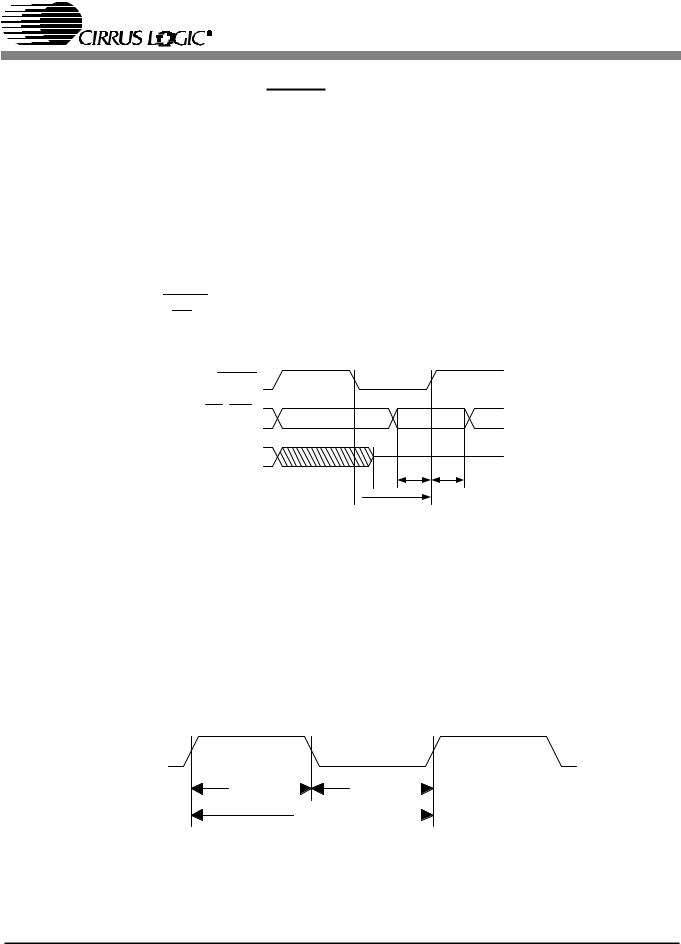
Figure 1. RESET Timing
1.6. Switching Characteristics — CLKIN
(TA = 25 °C; VA, VD[3:1] = 2.5 V ±5%; Inputs: Logic 0 = DGND, Logic 1 = VD, CL = 20 pF)
Parameter |
Symbol |
Min |
Max |
Unit |
|
|
|
|
|
CLKIN period for internal DSP clock mode |
Tclki |
35 |
3800 |
ns |
CLKIN high time for internal DSP clock mode |
Tclkih |
18 |
|
ns |
CLKIN low time for internal DSP clock mode |
Tclkil |
18 |
|
ns |
CLKIN
Tclkih |
|
|
Tclkil |
|
Tclki |
|
|||
|
|
|
||
|
|
|
||
Figure 2. CLKIN with CLKSEL = VSS = PLL Enable
DS339PP4 |
7 |

CS49300 Family DSP
1.7. Switching Characteristics — Intel® Host Mode
(TA = 25 °C; VA, VD[3:1] = 2.5 V ±5%; Inputs: Logic 0 = DGND, Logic 1 = VD, CL = 20 pF)
|
|
|
|
|
|
|
|
|
|
|
|
|
|
|
|
|
|
|
|
|
|
|
|
|
|
|
|
|
|
Parameter |
|
|
|
Symbol |
Min |
Max |
Unit |
|||||||||||||||||||||||||||||||||
|
|
|
|
|
|
|
|
|
|
|
|
|
|
|
|
|
|
|
|
|
|
|
|
|
|
|
|
|
|
|
|
|
|
|
|
|
|
|
|
|
|
|
|
|
|
|
|
|
|
|
|
|
|
|
|
|
|
|
|
|
|
|
|
|
|
|
|
|||
|
Address setup before |
|
|
|
|
|
|
|
|
and |
|
|
low or |
|
|
|
|
and |
|
|
|
low |
Tias |
5 |
- |
ns |
||||||||||||||||||||||||||||||||||||||||||||
|
CS |
|
|
RD |
CS |
|
WR |
|||||||||||||||||||||||||||||||||||||||||||||||||||||||||||||||
|
Address hold time after |
|
|
|
|
|
|
|
|
|
|
|
and |
|
|
|
|
low or |
|
|
|
|
and |
|
|
|
low |
Tiah |
5 |
- |
ns |
|||||||||||||||||||||||||||||||||||||||
|
CS |
|
|
RD |
|
CS |
WR |
|||||||||||||||||||||||||||||||||||||||||||||||||||||||||||||||
|
Delay between |
|
|
|
|
|
|
|
|
then |
|
|
|
|
|
|
|
|
|
|
low or |
|
|
|
|
then |
|
|
|
|
low |
|
|
|
Ticdr |
0 |
∞ |
ns |
||||||||||||||||||||||||||||||||
|
RD |
|
|
CS |
|
CS |
|
RD |
|
|
|
|||||||||||||||||||||||||||||||||||||||||||||||||||||||||||
|
Data valid after |
|
|
|
|
|
|
|
and |
|
|
|
|
|
|
|
|
|
low |
(Note 3) |
Tidd |
- |
21 |
ns |
||||||||||||||||||||||||||||||||||||||||||||||
|
CS |
|
RD |
|||||||||||||||||||||||||||||||||||||||||||||||||||||||||||||||||||
|
|
|
and |
|
|
|
|
low for read |
(Note 1) |
Tirpw |
DCLKP + 10 |
- |
ns |
|||||||||||||||||||||||||||||||||||||||||||||||||||||||||
|
CS |
|
RD |
|
||||||||||||||||||||||||||||||||||||||||||||||||||||||||||||||||||
|
Data hold time after |
|
|
|
|
|
|
|
or |
|
|
|
|
|
|
|
|
|
high |
|
|
|
Tidhr |
5 |
- |
ns |
||||||||||||||||||||||||||||||||||||||||||||
|
CS |
RD |
|
|
|
|
||||||||||||||||||||||||||||||||||||||||||||||||||||||||||||||||
|
Data high-Z after |
|
|
|
|
|
|
|
|
|
|
or |
|
|
|
|
|
|
|
|
|
high |
(Note 2) |
Tidis |
- |
22 |
ns |
|||||||||||||||||||||||||||||||||||||||||||
|
CS |
|
|
RD |
||||||||||||||||||||||||||||||||||||||||||||||||||||||||||||||||||
|
|
|
or |
|
|
|
high to |
|
|
|
|
|
|
|
|
|
and |
|
|
|
|
|
|
|
|
|
low for next read |
(Note 1) |
Tird |
2*DCLKP + 10 |
- |
ns |
||||||||||||||||||||||||||||||||||||||
|
CS |
|
RD |
|
CS |
|
RD |
|
||||||||||||||||||||||||||||||||||||||||||||||||||||||||||||||
|
|
|
or |
|
|
|
high to |
|
|
|
|
|
|
|
|
|
and |
|
|
|
|
|
|
|
|
|
|
|
low for next write |
(Note 1) |
Tirdtw |
2*DCLKP + 10 |
- |
ns |
||||||||||||||||||||||||||||||||||||
|
CS |
RD |
|
CS |
|
WR |
|
|||||||||||||||||||||||||||||||||||||||||||||||||||||||||||||||
|
Delay between |
|
|
|
|
|
|
|
|
then |
|
|
|
|
|
|
|
|
|
low or |
|
|
then |
|
|
|
low |
|
|
|
Ticdw |
0 |
∞ |
ns |
||||||||||||||||||||||||||||||||||||
|
WR |
CS |
CS |
WR |
|
|
|
|||||||||||||||||||||||||||||||||||||||||||||||||||||||||||||||
|
Data setup before |
|
|
|
|
|
|
|
|
|
or |
|
|
|
|
|
|
|
|
|
|
high |
|
|
|
Tidsu |
20 |
- |
ns |
|||||||||||||||||||||||||||||||||||||||||
|
CS |
|
WR |
|
|
|
||||||||||||||||||||||||||||||||||||||||||||||||||||||||||||||||
|
|
and |
|
|
|
|
low for write |
(Note 1) |
Tiwpw |
DCLKP + 10 |
- |
ns |
||||||||||||||||||||||||||||||||||||||||||||||||||||||||||
|
CS |
WR |
||||||||||||||||||||||||||||||||||||||||||||||||||||||||||||||||||||
|
Data hold after |
|
|
|
|
|
|
or |
|
|
|
|
|
|
|
|
high |
|
|
|
Tidhw |
5 |
- |
ns |
||||||||||||||||||||||||||||||||||||||||||||||
|
CS |
WR |
|
|
|
|||||||||||||||||||||||||||||||||||||||||||||||||||||||||||||||||
|
|
or |
|
|
|
high to |
|
|
|
|
|
|
|
|
and |
|
|
|
|
|
|
|
|
|
|
low for next read |
(Note 1) |
Tiwtrd |
2*DCLKP + 10 |
- |
ns |
|||||||||||||||||||||||||||||||||||||||
|
CS |
WR |
CS |
RD |
|
|||||||||||||||||||||||||||||||||||||||||||||||||||||||||||||||||
|
|
|
or |
|
|
|
high to |
|
|
|
|
|
|
|
|
and |
|
|
|
|
|
|
|
|
|
|
low for next write |
(Note 1) |
Tiwd |
2*DCLKP + 10 |
- |
ns |
||||||||||||||||||||||||||||||||||||||
|
CS |
WR |
CS |
WR |
||||||||||||||||||||||||||||||||||||||||||||||||||||||||||||||||||
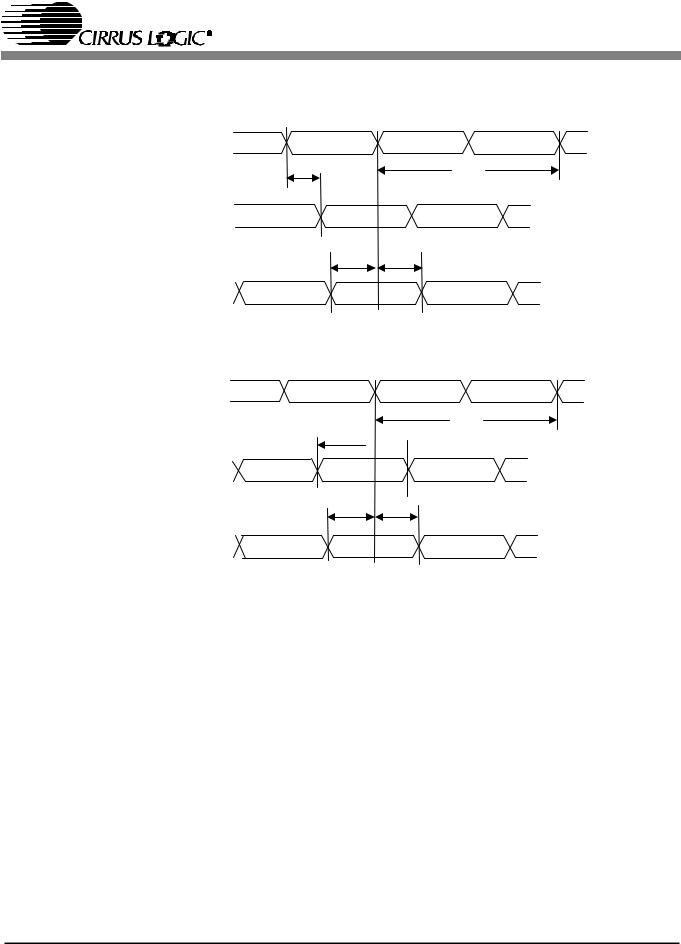
Notes: 1. Certain timing parameters are normalized to the DSP clock, DCLKP, in nanoseconds. DCLKP = 1/DCLK. The DSP clock can be defined as follows:
External CLKIN Mode:
DCLK == CLKIN/4 before and during boot
DCLK == CLKIN after boot
Internal Clock Mode:
DCLK == 10MHz before and during boot, i.e. DCLKP == 100ns
DCLK == 65 MHz after boot, i.e. DCLKP == 15.4ns
It should be noted that DCLK for the internal clock mode is application specific. The application code users guide should be checked to confirm DCLK for the particular application.
2.This specification is characterized but not production tested. A 470 ohm pull-up resistor was used for characterization to minimize the effects of external bus capacitance.
3.See Tidd from Intel Host Mode in Table 6 on page 43
8 |
DS339PP4 |
CS49300 Family DSP
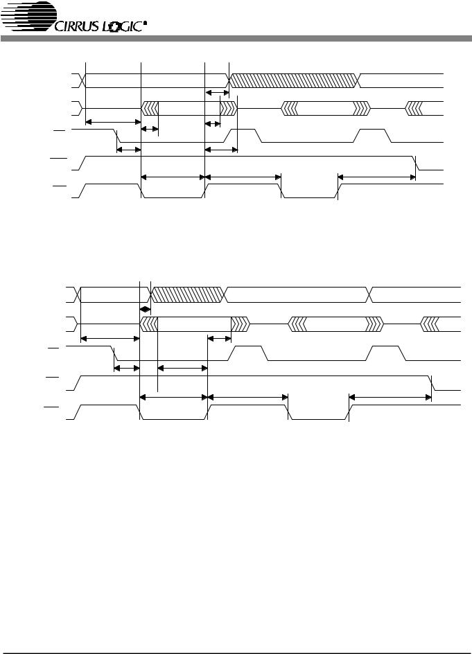
A1:0 |
|
|
Tia h |
DA TA7:0 |
|
Tias |
|
Tidhr |
|
Tidd |
|
CS |
|
Ticdr |
Tidis |
W R |
|
Tirpw |
Tird |
RD |
|
Figure 3. Intel® Parallel Host Mode Read Cycle
A1:0 |
|
Tiah |
|
DATA7:0 |
|
Tias |
Tidhw |
|
|
CS |
|
Ticdw |
Tidsu |
RD |
Tiw d |
Tiw p w |
|
W R |
|
Figure 4. Intel® Parallel Host Mode Write Cycle
Tirdtw
Tiw trd
DS339PP4 |
9 |

CS49300 Family DSP
1.8. Switching Characteristics — Motorola® Host Mode
(TA = 25 °C; VA, VD[3:1] = 2.5 V ±5%; Inputs: Logic 0 = DGND, Logic 1 = VD, CL = 20 pF)
|
|
|
|
|
|
|
|
|
|
|
|
|
|
|
|
|
|
|
|
|
|
|
|
|
|
|
|
|
|
|
|
|
|
|
|
Parameter |
|
Symbol |
Min |
Max |
Unit |
||||||||||||||||||||||||||||
|
|
|
|
|
|
|
|
|
|
|
|
|
|
|
|
|
|
|
|
|
|
|
|
|
|
|
|
|
|
|
|
|
|
|
|
|
|
|
|
|
|
|
|
|
|
|
|
|
|
|
|
|
|
|
|
|
|
|
|
|
|
|
|
|
|
|
|
||
|
Address setup before |
|
|
|
|
|
|
|
|
|
and |
|
|
|
low |
|
Tmas |
5 |
- |
ns |
|||||||||||||||||||||||||||||||||||||||||||||||||
|
CS |
|
|
DS |
|
||||||||||||||||||||||||||||||||||||||||||||||||||||||||||||||||
|
Address hold time after |
|
|
|
|
|
|
|
|
|
|
|
|
and |
|
|
|
low |
|
Tmah |
5 |
- |
ns |
||||||||||||||||||||||||||||||||||||||||||||||
|
CS |
|
|
|
DS |
|
|||||||||||||||||||||||||||||||||||||||||||||||||||||||||||||||
|
Delay between |
|
|
|
|
|
|
|
|
then |
|
|
|
|
|
|
|
|
|
|
low or |
|
|
then |
|
low |
|
Tmcdr |
0 |
∞ |
ns |
||||||||||||||||||||||||||||||||||||||
|
DS |
|
|
CS |
CS |
DS |
|
||||||||||||||||||||||||||||||||||||||||||||||||||||||||||||||
|
Data valid after |
|
|
|
|
|
|
|
and |
|
|
|
|
|
|
|
|
|
|
|
|
|
|
|
|
|
|
|
|
|
|
|
|
|
|
|
|
|
|
|
Tmdd |
- |
21 |
ns |
|||||||||||||||||||||||||
|
CS |
RD |
|
low with R/W |
high |
(Note 3) |
|||||||||||||||||||||||||||||||||||||||||||||||||||||||||||||||
|
|
|
|
|
|
|
|
|
|
|
|
|
|
|
|
|
|
|
|
|
|
|
|
|
|
|
|
|
|
|
|
|
|
|
|
|
|
|
|
|
|
|
|
|
|
|
|
||||||||||||||||||||||
|
|
|
|
and |
|
|
|
low for read |
(Note 1) |
Tmrpw |
DCLKP + 10 |
- |
ns |
||||||||||||||||||||||||||||||||||||||||||||||||||||||||
|
CS |
|
DS |
||||||||||||||||||||||||||||||||||||||||||||||||||||||||||||||||||
|
Data hold time after |
|
|
|
|
|
|
|
|
|
or |
|
|
|
|
|
|
|
|
|
|
|
high after read |
|
Tmdhr |
5 |
- |
ns |
|||||||||||||||||||||||||||||||||||||||||
|
CS |
DS |
|
|
|||||||||||||||||||||||||||||||||||||||||||||||||||||||||||||||||
|
Data high-Z after |
|
|
|
|
|
|
|
|
|
|
or |
|
|
|
|
|
|
|
|
|
|
high low after read |
(Note 2) |
Tmdis |
- |
22 |
ns |
|||||||||||||||||||||||||||||||||||||||||
|
CS |
DS |
|
||||||||||||||||||||||||||||||||||||||||||||||||||||||||||||||||||
|
|
|
|
or |
|
|
|
high to |
|
|
|
|
|
|
|
|
|
and |
|
|
|
|
|
|
|
|
|
|
low for next read |
(Note 1) |
Tmrd |
2*DCLKP + 10 |
- |
ns |
|||||||||||||||||||||||||||||||||||
|
CS |
|
DS |
CS |
DS |
|
|||||||||||||||||||||||||||||||||||||||||||||||||||||||||||||||
|
|
|
|
or |
|
|
|
high to |
|
|
|
|
|
|
|
|
|
and |
|
|
|
|
|
|
|
|
|
|
low for next write |
(Note 1) |
Tmrdtw |
2*DCLKP + 10 |
- |
ns |
|||||||||||||||||||||||||||||||||||
|
CS |
DS |
CS |
DS |
|
||||||||||||||||||||||||||||||||||||||||||||||||||||||||||||||||
|
Delay between |
|
|
|
|
|
|
|
then |
|
|
|
|
|
|
|
|
|
|
low or |
|
|
then |
|
low |
|
Tmcdw |
0 |
∞ |
ns |
|||||||||||||||||||||||||||||||||||||||
|
DS |
CS |
CS |
DS |
|
||||||||||||||||||||||||||||||||||||||||||||||||||||||||||||||||
|
Data setup before |
|
|
|
|
|
|
|
|
|
|
|
or |
|
|
|
|
|
|
|
|
|
|
|
high |
|
Tmdsu |
20 |
- |
ns |
|||||||||||||||||||||||||||||||||||||||
|
CS |
|
DS |
|
|
||||||||||||||||||||||||||||||||||||||||||||||||||||||||||||||||
|
|
|
and |
|
|
|
low for write |
(Note 1) |
Tmwpw |
DCLKP + 10 |
- |
ns |
|||||||||||||||||||||||||||||||||||||||||||||||||||||||||
|
CS |
DS |
|||||||||||||||||||||||||||||||||||||||||||||||||||||||||||||||||||
|
|
|
|
|
|
setup before |
|
|
|
|
|
|
|
|
|
|
|
|
AND |
|
|
|
|
|
|
|
|
low |
|
Tmrwsu |
5 |
- |
ns |
||||||||||||||||||||||||||||||||||||
|
R/W |
|
CS |
|
DS |
|
|||||||||||||||||||||||||||||||||||||||||||||||||||||||||||||||
|
|
|
|
|
|
hold time after |
|
|
|
|
|
|
|
|
|
or |
|
|
|
|
|
|
|
|
|
high |
|
Tmrwhld |
5 |
- |
ns |
||||||||||||||||||||||||||||||||||||||
|
R/W |
CS |
DS |
|
|||||||||||||||||||||||||||||||||||||||||||||||||||||||||||||||||
|
Data hold after |
|
|
|
|
|
|
or |
|
|
|
|
|
|
|
|
|
high |
|
Tmdhw |
5 |
- |
ns |
||||||||||||||||||||||||||||||||||||||||||||||
|
CS |
DS |
|
|
|||||||||||||||||||||||||||||||||||||||||||||||||||||||||||||||||
|
|
|
or |
|
|
|
high to |
|
|
|
|
|
|
|
|
|
and |
|
|
|
|
|
|
|
|
|
|
|
|
|
|
|
|
|
|
|
|
|
|
|
high for next read |
Tmwtrd |
2*DCLKP + 10 |
- |
ns |
||||||||||||||||||||||||
|
CS |
DS |
CS |
DS |
low with R/W |
||||||||||||||||||||||||||||||||||||||||||||||||||||||||||||||||
|
|
|
|
|
|
|
|
|
|
|
|
|
|
|
|
|
|
|
|
|
|
|
|
|
|
|
|
|
|
|
|
|
|
|
|
|
|
|
|
|
|
|
|
|
|
|
|
|
|
|
|
|
|
|
|
|
|
|
|
|
|
|
|
|
(Note 1) |
|
|
|
|
|
|
|
|
|
|
|
|||||||||||||||||||||||||||||||||||||||||||||||||||||||||||||||
|
|
|
or |
|
|
|
high to |
|
|
|
|
|
|
|
|
|
and |
|
|
|
|
|
|
|
|
|
low for next write |
(Note 1) |
Tmwd |
2*DCLKP + 10 |
- |
ns |
|||||||||||||||||||||||||||||||||||||
|
CS |
DS |
CS |
DS |
|||||||||||||||||||||||||||||||||||||||||||||||||||||||||||||||||
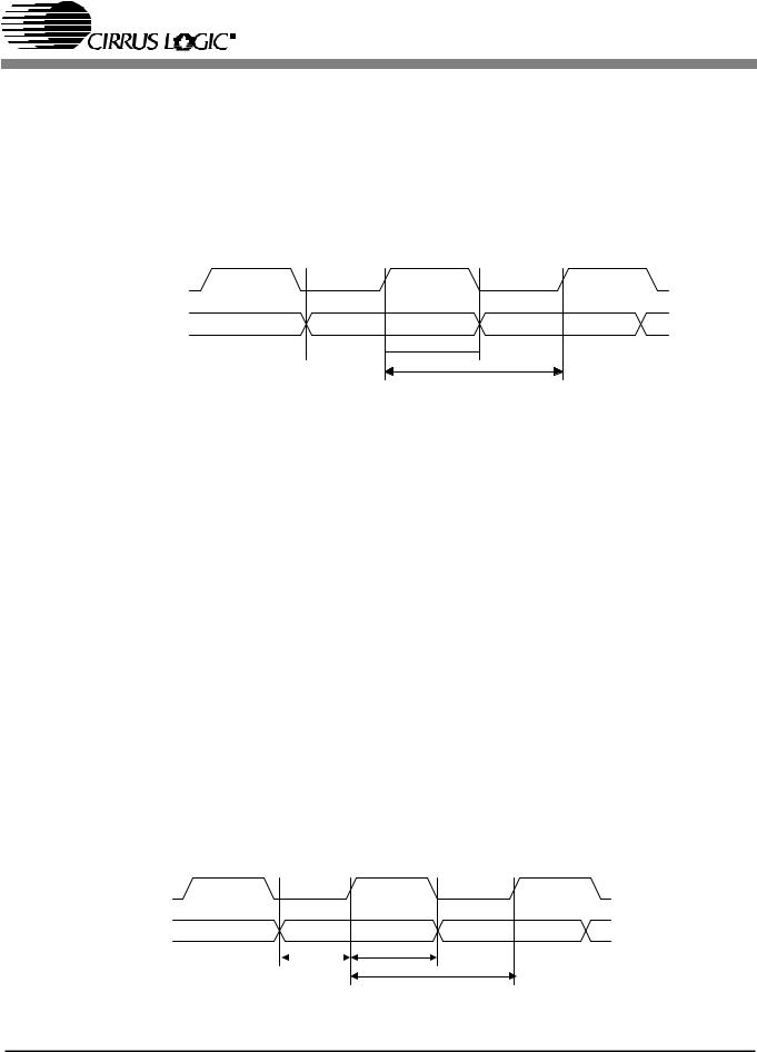
Notes: 1. Certain timing parameters are normalized to the DSP clock, DCLKP, in nanoseconds. DCLKP = 1/DCLK. The DSP clock can be defined as follows:
External CLKIN Mode:
DCLK == CLKIN/4 before and during boot
DCLK == CLKIN after boot
Internal Clock Mode:
DCLK == 10MHz before and during boot, i.e. DCLKP == 100ns
DCLK == 65 MHz after boot, i.e. DCLKP == 15.4ns
It should be noted that DCLK for the internal clock mode is application specific. The application code users guide should be checked to confirm DCLK for the particular application.
2.This specification is characterized but not production tested. A 470 ohm pull-up resistor was used for characterization to minimize the effects of external bus capacitance.
3.See Tmdd from Motorola Host Mode in Table 7 on page 45
10 |
DS339PP4 |

CS49300 Family DSP
A1:0 |
|
|
|
|
|
Tm ah |
|
DATA7:0 |
Tm as |
|
|
|
Tm dhr |
|
|
|
|
|
|
CS |
Tm rw su |
Tm dd |
|
|
|
||
|
Tm cdr |
Tm dis |
|
|
|
||
R/W |
|
Tm rpw |
Tm rd |
|
|
||
DS |
|
|
|
Tm rw hld |
Tm rdtw |
Figure 5. Motorola® Parallel Host Mode Read Cycle
A 1 |
:0 |
|
|
Tm as |
Tm ah |
D A T A 7 |
:0 |
|
|
Tm d su |
Tm dhw |
C S |
|
|
|
Tm cdw |
Tm w pw |
R /W |
|
|
|
Tm rw su |
Tm w d |
D S |
|
|
 Tm rw h ld
 Tm w trd
Figure 6. Motorola® Parallel Host Mode Write Cycle
DS339PP4 |
11 |

CS49300 Family DSP
1.9. Switching Characteristics — SPI Control Port
(TA = 25 °C; VA, VD[3:1] = 2.5 V ±5%; Inputs: Logic 0 = DGND, Logic 1 = VD, CL = 20 pF)
|
|
|
|
|
|
|
|
|
|
|
|
Parameter |
|
Symbol |
Min |
Max |
Units |
||
|
|
|
|
|
|
|
|||||||||||||
|
SCCLK clock frequency |
(Note 1) |
fsck |
- |
2000 |
kHz |
|||||||||||||
|
|
falling to SCCLK rising |
|
tcss |
20 |
- |
ns |
||||||||||||
|
CS |
|
|||||||||||||||||
|
Rise time of SCCLK line |
(Note 7) |
tr |
- |
50 |
ns |
|||||||||||||
|
Fall time of SCCLK lines |
(Note 7) |
tf |
- |
50 |
ns |
|||||||||||||
|
SCCLK low time |
|
tscl |
150 |
- |
ns |
|||||||||||||
|
SCCLK high time |
|
tsch |
150 |
- |
ns |
|||||||||||||
|
Setup time SCDIN to SCCLK rising |
|
tcdisu |
50 |
- |
ns |
|||||||||||||
|
Hold time SCCLK rising to SCDIN |
(Note 2) |
tcdih |
50 |
- |
ns |
|||||||||||||
|
Transition time from SCCLK to SCDOUT valid |
(Note 3) |
tscdov |
- |
40 |
ns |
|||||||||||||
|
Time from SCCLK rising to |
|
|
|
|
rising |
(Note 4) |
tscrh |
- |
200 |
ns |
||||||||
|
INTREQ |
||||||||||||||||||
|
Rise time for |
|
|
|
|
|
|
|
|
|
|
|
(Note 4) |
trr |
- |
(Note 6) |
ns |
||
|
INTREQ |
|
|
|
|
|
|
||||||||||||
|
Hold time for |
|
|
|
from SCCLK rising |
(Note 5, 7) |
tscrl |
0 |
- |
ns |
|||||||||
|
INTREQ |
||||||||||||||||||
|
Time from SCCLK falling to |
|
|
rising |
|
tsccsh |
20 |
- |
ns |
||||||||||
|
CS |
|
|||||||||||||||||
|
High time between active |
|
|
|
|
|
|
|
tcsht |
200 |
- |
ns |
|||||||
|
CS |
|
|
||||||||||||||||
|
Time from |
|
|
|
rising to SCDOUT high-Z |
(Note 7) |
tcscdo |
|
20 |
ns |
|||||||||
|
CS |
|
|||||||||||||||||
Notes: 1. The specification fsck indicates the maximum speed of the hardware. The system designer should be aware that the actual maximum speed of the communication port may be limited by the software. The relevant application code user’s manual should be consulted for the software speed limitations.
2.Data must be held for sufficient time to bridge the 50 ns transition time of SCCLK.
3.SCDOUT should not be sampled during this time period.
4.INTREQ goes high only if there is no data to be read from the DSP at the rising edge of SCCLK for the second-to-last bit of the last byte of data during a read operation as shown.
5.If INTREQ goes high as indicated in (Note 4), then INTREQ is guaranteed to remain high until the next rising edge of SCCLK. If there is more data to be read at this time, INTREQ goes active low again. Treat this condition as a new read transaction. Raise chip select to end the current read transaction and then drop it, followed by the 7-bit address and the R/W bit (set to 1 for a read) to start a new read transaction.
6.With a 4.7k Ohm pull-up resistor this value is typically 215ns. As this pin is open drain adjusting the pull up value will affect the rise time.
7.This time is by design and not tested.
12 |
DS339PP4 |
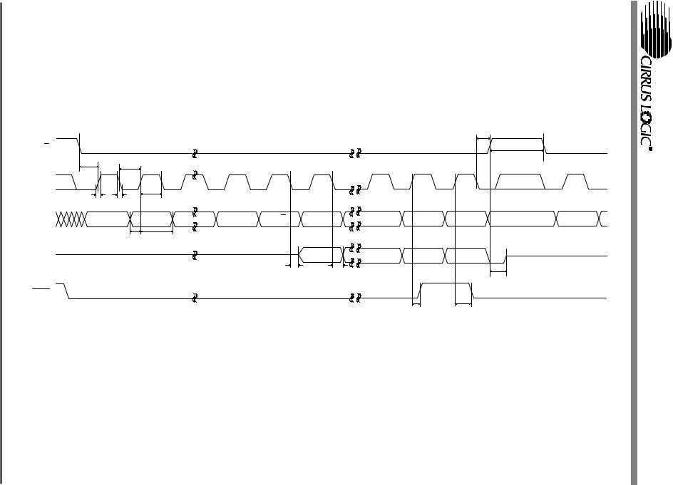
DS339PP4
C S
S C C L K
S C D IN
S C D O U T
IN T R E Q
13
|
|
|
|
|
|
|
|
|
ts c c s h |
tc s s |
ts c l |
|
|
|
|
|
|
|
tc s h t |
0 |
1 |
2 |
6 |
7 |
0 |
5 |
6 |
7 |
|
tr |
ts c h |
|
|
|
|
|
|
|
|
tf |
|
|
|
|
|
|
|
|
|
A 6 |
A 5 |
|
A 0 |
R /W |
M S B |
|
|
L S B |
A 6 |
|
t c d is u t c d ih |
|
|
|
|
|
|
|
|
|
|
|
|
|
M S B |
|
|
L S B |
tri-s ta te |
|
|
|
|
|
|
|
|
|
|
|
|
|
|
ts c d o v |
|
ts c d o v |
|
|
tc s c d o |
|
|
|
|
|
|
|
|
|
|
|
|
|
|
|
|
|
ts c rh |
ts c rl |
|
Figure 7. SPI Control Port Timing
DSP Family CS49300

CS49300 Family DSP
1.10. Switching Characteristics — I2C® Control Port
(TA = 25 °C; VA, VD[3:1] = 2.5 V ±5%; Inputs: Logic 0 = DGND, Logic 1 = VD, CL = 20 pF)
|
|
|
|
|
Parameter |
|
Symbol |
Min |
Max |
Units |
|
|
|
|
|
|
|
||||||
SCCLK clock frequency |
(Note 1) |
fscl |
|
400 |
kHz |
||||||
Bus free time between transmissions |
|
tbuf |
4.7 |
|
s |
||||||
Start-condition hold time (prior to first clock pulse) |
|
thdst |
4.0 |
|
s |
||||||
Clock low time |
|
tlow |
1.2 |
|
s |
||||||
Clock high time |
|
thigh |
1.0 |
|
s |
||||||
SCDIO setup time to SCCLK rising |
|
tsud |
250 |
|
ns |
||||||
SCDIO hold time from SCCLK falling |
(Note 2) |
thdd |
0 |
|
s |
||||||
Rise time of SCCLK |
(Note 3), (Note 7) |
tr |
|
50 |
ns |
||||||
Fall time of SCCLK |
(Note 7) |
tf |
|
300 |
ns |
||||||
Time from SCCLK falling to CS493XX ACK |
|
tsca |
|
40 |
ns |
||||||
Time from SCCLK falling to SCDIO valid during read operation |
tscsdv |
|
40 |
ns |
|||||||
Time from SCCLK rising to |
|
rising |
(Note 4) |
tscrh |
|
200 |
ns |
||||
INTREQ |
|
||||||||||
Hold time for |
|
|
from SCCLK rising |
(Note 5) |
tscrl |
0 |
|
ns |
|||
INTREQ |
|
||||||||||
Rise time for |
|
|
|
|
|
|
(Note 6) |
trr |
|
** |
ns |
INTREQ |
|
|
|||||||||
Setup time for stop condition |
|
tsusp |
4.7 |
|
s |
||||||
Notes:. 1. The specification fscl indicates the maximum speed of the hardware. The system designer should be aware that the actual maximum speed of the communication port may be limited by the software. The relevant application code user’s manual should be consulted for the software speed limitations.
2.Data must be held for sufficient time to bridge the 300-ns transition time of SCCLK. This hold time is by design and not tested.
3.This rise time is shorter than that recommended by the I2C specifications. For more information, see Section 6.1, “Serial Communication” on page 33.
4.INTREQ goes high only if there is no data to be read from the DSP at the rising edge of SCCLK for the last data bit of the last byte of data during a read operation as shown.
5.If INTREQ goes high as indicated in Note 8, then INTREQ is guaranteed to remain high until the next rising edge of SCCLK. If there is more data to be read at this time, INTREQ goes active low again. Treat this condition as a new read transaction. Send a new start condition followed by the 7-bit address and the R/W bit (set to 1 for a read). This time is by design and is not tested.
6.With a 4.7k Ohm pull-up resistor this value is typically 215ns. As this pin is open drain adjusting the pull up value will affect the rise time.
7.This time is by design and not tested.
14 |
DS339PP4 |
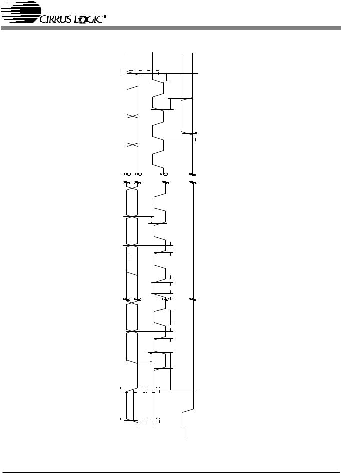
CS49300 Family DSP
stop |
|
susp |
|
|
t |
ACK |
8 |
scrl |
|
|
t |
LSB |
7 |
scrh |
|
|
t |
|
MSB |
|
0 |
|
|
ACK |
scsdv |
|
|
|
t |
8 |
|
|
|
|
|
|
sca |
|
R/W |
|
|
t |
|
|
7 |
|
|
|
|
|
|
f |
|
|
|
|
t |
|
A0 |
|
6 |
|
|
|
|
|
r |
|
|
|
|
t |
|
A5 |
|
1 |
high |
|
|
t |
||
|
|
|
|
hdd |
|
|
|
|
t |
|
A6 |
sud |
0 |
|
|
|
|
low |
|
|
|
t |
|
|
|
|
|
|
t |
|
|
|
|
hdst |
start |
|
|
|
t |
|
|
|
|
|
|
|
buf |
|
|
|
|
t |
|
|
stop |
SCDIO |
|
SCCLK |
INTREQ |
Figure 8. I2C® Control Port Timing
DS339PP4 |
15 |

CS49300 Family DSP
1.11. Switching Characteristics — Digital Audio Input
(TA = 25 °C; VA, VD[3:1] = 2.5 V ±5%; Inputs: Logic 0 = DGND, Logic 1 = VD, CL = 20 pF)
Parameter |
|
Symbol |
Min |
Max |
Unit |
|
|
|
|
|
|
SCLKN1(2) period for both Master and Slave mode |
(Note 1) |
Tsclki |
40 |
- |
ns |
SCLKN1(2) duty cycle for Master and Slave mode |
(Note 1) |
|
45 |
55 |
% |
|
|
|
|
|
|
Master Mode |
(Note 1, 2) |
|
|
|
|
|
|
|
|
|
|
LRCLKN1(2) delay after SCLKN1(2) transition |
(Note 3) |
Tlrds |
- |
10 |
ns |
SDATAN1(2) setup to SCLKN1(2) transition |
(Note 4) |
Tsdsum |
10 |
- |
ns |
SDATAN1(2) hold time after SCLKN1(2) transition |
(Note 4) |
Tsdhm |
5 |
- |
ns |
Slave Mode |
(Note 5) |
|
|
|
|
|
|
|
|
|
|
Time from active edge of SCLKN1(2) to LRCLKN1(2) transition |
Tstlr |
10 |
- |
ns |
|
Time from LRCLKN1(2) transition to SCLKN1(2) active edge |
|
Tlrts |
10 |
- |
ns |
SDATAN1(2) setup to SCLKN1(2) transition |
(Note 4) |
Tsdsus |
5 |
- |
ns |
SDATAN1(2) hold time after SCLKN1(2) transition |
(Note 4) |
Tsdhs |
5 |
- |
ns |
Notes: 1. Master mode timing specifications are characterized, not production tested.
2.Master mode is defined as the CS493XX driving LRCLKN1(2) and SCLKN1(2). Master or Slave mode can be programmed.
3.This timing parameter is defined from the non-active edge of SCLKN1(2). The active edge of SCLKN1(2) is the point at which the data is valid.
4.This timing parameter is defined from the active edge of SCLKN1(2). The active edge of SCLKN1(2) is the point at which the data is valid.
5.Slave mode is defined as SCLKN1(2) and LRCLKN1(2) being driven by an external source.
16 |
DS339PP4 |
CS49300 Family DSP
M ASTER M O DE
S C LK N 1
S C LK N 2
Tlrds |
Tsclki |
|
LR C LK N 1
LR C LK N 2
Tsdsum Tsdhm
S D A TA N 1
S D A TA N 2
SLAVE M O DE
S C LK N 1
S C LK N 2
Tsclki
Tlrts 
 Tstlr
Tstlr
LR C LK N 1
LR C LK N 2
Tsdsus Tsdhs
S D A TA N 1
S D A TA N 2
Figure 9. Digital Audio Input Data, Master and Slave Clock Timing
DS339PP4 |
17 |
CS49300 Family DSP
1.12. Switching Characteristics — CMPDAT, CMPCLK
(TA = 25 °C; VA, VD[3:1] = 2.5 V ±5%; Inputs: Logic 0 = DGND, Logic 1 = VD, CL = 20 pF)
Parameter |
Symbol |
Min |
Max |
Unit |
|
|
|
|
|
Serial compressed data clock CMPCLK period |
Tcmpclk |
- |
27 |
MHz |
CMPDAT setup before CMPCLK high |
Tcmpsu |
5 |
- |
ns |
CMPDAT hold after CMPCLK high |
Tcmphld |
3 |
- |
ns |
CMPCLK
CMPDAT
Tcm ps u 

 Tcm p hld
Tcm p clk
Figure 10. Serial Compressed Data Timing
1.13. Switching Characteristics — Parallel Data Input
(TA = 25 °C; VA, VD[3:1] = 2.5 V ±5%; Inputs: Logic 0 = DGND, Logic 1 = VD, CL = 20 pF)
Parameter |
Symbol |
Min |
Max |
Unit |
|
|
|
|
|
CMPCLK Period |
Tcmpclk |
4*DCLK + 10 |
|
ns |
DATA[7:0] setup before CMPCLK high |
Tcmpsu |
10 |
|
ns |
DATA[7:0] hold after CMPCLK high |
Tcmphld |
10 |
|
ns |
Notes: 1. Certain timing parameters are normalized to the DSP clock, DCLK, in nanoseconds. The DSP clock can be defined as follows:
External CLKIN Mode:
DCLK == CLKIN/4 before and during boot
DCLK == CLKIN after boot
Internal Clock Mode:
DCLK == 10MHz before and during boot, i.e. DCLK == 100ns
DCLK == 65 MHz after boot, i.e. DCLK == 15.4ns
It should be noted that DCLK for the internal clock mode is application specific. The application code users guide should be checked to confirm DCLK for the particular application.
C M PC LK
D AT A[7:0]
Tcm psu |
|
Tcm phld |
|
Tcm pclk
Figure 11. Parallel Data Timing (when not in a parallel control mode)
18 |
DS339PP4 |

CS49300 Family DSP
1.14. Switching Characteristics — Digital Audio Output
(TA = 25 °C; VA, VD[3:1] = 2.5 V ±5%; Inputs: Logic 0 = DGND, Logic 1 = VD, CL = 20 pF)
Parameter |
|
Symbol |
Min |
Max |
Unit |
|
|
|
|
|
|
MCLK period |
(Note 1) |
Tmclk |
40 |
- |
ns |
MCLK duty cycle |
(Note 1) |
|
40 |
60 |
% |
|
|
|
|
|
|
SCLK period for Master or Slave mode |
(Note 2) |
Tsclk |
40 |
- |
ns |
SCLK duty cycle for Master or Slave mode |
(Note 2) |
|
45 |
55 |
% |
|
|
|
|
|
|
Master Mode |
(Note 2, 3) |
|
|
|
|
|
|
|
|
|
|
SCLK delay from MCLK rising edge, MCLK as an input |
Tsdmi |
|
15 |
ns |
|
SCLK delay from MCLK rising edge, MCLK as an output |
Tsdmo |
–5 |
10 |
ns |
|
LRCLK delay from SCLK transition |
(Note 4) |
Tlrds |
|
10 |
ns |
AUDATA2–0 delay from SCLK transition |
(Note 4) |
Tadsm |
|
10 |
ns |
Slave Mode |
(Note 5) |
|
|
|
|
|
|
|
|
|
|
Time from active edge of SCLKN1(2) to LRCLKN1(2) transition |
Tstlr |
10 |
- |
ns |
|
Time from LRCLKN1(2) transition to SCLKN1(2) active edge |
Tlrts |
10 |
- |
ns |
|
AUDATA2–0 delay from SCLK transition |
(Note 4, 6) |
Tadss |
|
15 |
ns |
Notes: 1. MCLK can be an input or an output. These specifications apply for both cases.
2.Master mode timing specifications are characterized, not production tested.
3.Master mode is defined as the CS493XX driving both SCLK and LRCLK. When MCLK is an input, it is divided to produce SCLK and LRCLK.
4.This timing parameter is defined from the non-active edge of SCLK. The active edge of SCLK is the point at which the data is valid.
5.Slave mode is defined as SCLK and LRCLK being driven by an external source.
6.This specification is characterized, not production tested.
DS339PP4 |
19 |
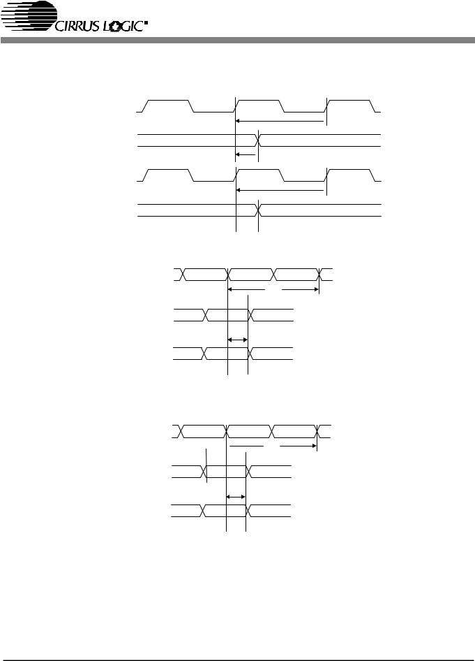
CS49300 Family DSP
MCLK (Input)
 T mclk
SCLK (Output)
 T sdmi
MCLK (Output)
 T mclk
SCLK (Output)

 T sdmo
MASTER MODE
SCLK
Tsclk

 Tlrds
Tlrds
LRCLK
Tadsm
AUDATA2:0
SLAVE MODE
SCLK
Tlrts  Tsclk
Tsclk


 Tstlr
Tstlr
LRCLK
Tadss
AUDATA2:0
Figure 12. Digital Audio Output Data, Input and Output Clock Timing
20 |
DS339PP4 |
2.FAMILY OVERVIEW
The CS49300 family contains system on a chip solutions for multichannel audio decompression and digital signal processing. The CS49300 family is split into 4 sub-families targeted at the DVD, broadcast and audio/video receiver (AVR), and effects and post processing markets.
This document focuses on the electrical features and characteristics of these parts. Different features are described from a hardware design perspective. It should be understood that not all of the features portrayed in this document are supported by all of the versions of application code available. The application code user’s guides should be consulted to confirm which hardware features are supported by the software.
The parts use a combination of internal ROM and RAM. Depending on the application being used, a download of application software may be required each time the part is powered up. This document uses “download” and “code load” interchangeably. These terms should be interpreted as meaning the transfer of application code into the internal memory of the part from either an external microcontroller or through the autoboot procedure.
2.1. Multichannel Decoder Family of Parts
CS49300 - DVD Audio Decoder. The CS49300 device is targeted at audio decoding in the DVD via ES or PES in a serial or parallel bursty fashion for MLP or for DVD Audio Pack Layer Support. (All the other decoding/processing algorithms listed below require delivery of PCM or IEC61937packed compressed data via I2S or LJ formatted digital audio to the CS49300). Specifically the CS49300 will support all of the following decoding/processing standards:
•Meridian Lossless Packing™ (MLP™)* (for ES and PES data delivery only)
•DVD Audio Pack Layer Support* (for ES and PES data delivery only)
CS49300 Family DSP
•Dolby Digital™ (AC-3™) with Dolby Pro Logic™
•Dolby Digital™ with Dolby Pro Logic™ plus Cirrus Extra Surround™
•Dolby Digital™ with Dolby Pro Logic II™
•Dolby Digital™ with Dolby Pro Logic II™ plus Cirrus Extra Surround™
•Virtual Dolby Digital™
•MPEG-2, Advanced Audio Coding Algorithm (AAC)
•MPEG Multichannel
•MPEG Multichannel with Dolby Pro Logic II™
•MPEG Multichannel plus Cirrus Extra Surround™
•MPEG-1, Layer 3 (MP3)
•DTS Digital Surround™
•DTS Digital Surround™ with Dolby Pro Logic II™
•DTS Digital Surround™ plus Cirrus Extra Surround™
•DTS-ES Extended Surround™ (DTS-ES Discrete 6.1 & Matrix 6.1)
•DTS Neo:6™
•LOGIC5® (5.1 Channel, Max Fs=48kHz and LOGIC7® (7.1 Channel, Max Fs=96kHz)
•VMAx VirtualTheater® (Virtual Dolby Digital)
•SRS TruSurround™ (Virtual Dolby Digital and DTS Virtual 5.1™ Versions)
•SRS Circle Surround™ I/II
•HDCD®
•Cirrus P.D.F. (Dolby Pro Logic 2Fs Decoder and PCM Upsampler)
•Cirrus PL2_2FS (Dolby Pro Logic II 2Fs Decoder and PCM Upsampler)
Please refer to the CS4932x/CS49330 Part Matrix vs. Code Matrix (PDF) document available from the CS49300 Web Site Page for the latest listing of audio decoding/processing algorithms. The part
DS339PP4 |
21 |

will also support PES layer decode for audio/video synchronization and DVD Audio Pack layer support. The CS49300 will support all of the above decoding and PCM processing standards.
CS4931X - Broadcast Sub-family. The CS4931X sub-family is targeted at audio decoding in the broadcast markets in systems such as digital TV, HDTV, set-top boxes and digital audio broadcast units (digital radios). Specifically the CS4931X sub-family will support the following decode standards:
•Dolby Digital™ (AC-3™) with Dolby Pro Logic™
•MPEG-2, Advanced Audio Coding Algorithm (AAC)
•MPEG-1, Layers 1, 2 Stereo
•MPEG-1, Layers 3 (MP3) Stereo
•MPEG-2, Layer 2 Stereo
•MPEG-2, Layer 3 (MP3) Stereo
The part will also support PES layer decode for audio/video synchronization. The CS49310 will support all of the above decode standards while other parts in the CS4931X sub-family will decode subsets of the above audio decoding standards.
CS4932X - Audio/Video Receiver (AVR) Subfamily. The CS4932X sub-family is targeted at audio decoding in the audio/video receiver markets. Typical applications will include amplifiers with integrated decoding capability, outboard decoder pre-amplifiers, car radios and any system where the compressed audio is received in an IEC61937 format. Specifically the CS4932X sub-family will support the following decode standards:
•Dolby Digital™ (AC-3™) with Dolby Pro Logic™
•Dolby Digital™ with Dolby Pro Logic™ plus Cirrus Extra Surround™
•Dolby Digital™ with Dolby Pro Logic II™
CS49300 Family DSP
•Dolby Digital™ with Dolby Pro Logic II™ plus Cirrus Extra Surround™
•Virtual Dolby Digital™
•MPEG-2, Advanced Audio Coding Algorithm (AAC)
•MPEG Multichannel
•MPEG Multichannel with Dolby Pro Logic II™
•MPEG Multichannel plus Cirrus Extra Surround™
•MPEG-1, Layer 3 (MP3)
•DTS Digital Surround™
•DTS Digital Surround™ with Dolby Pro Logic II™
•DTS Digital Surround™ plus Cirrus Extra Surround™
•DTS-ES Extended Surround™ (DTS-ES Discrete 6.1 & Matrix 6.1)
•DTS Neo:6™
•LOGIC5® (5.1 Channel, Max Fs=48kHz and LOGIC7® (7.1 Channel, Max Fs=96kHz)
•VMAx VirtualTheater® (Virtual Dolby Digital)
•SRS TruSurround™ (Virtual Dolby Digital and DTS Virtual 5.1™ Versions)
•SRS Circle Surround™ I/II
•HDCD®
•Cirrus P.D.F. (Dolby Pro Logic 2Fs Decoder and PCM Upsampler)
•Cirrus PL2_2FS (Dolby Pro Logic II 2Fs Decoder and PCM Upsampler)
The CS49326 will support all of the above decode standards while other parts in the CS4932X subfamily will decode subsets of the above audio decoding standards.
Except for the CS49329 which offers AAC support this subfamily will offer integrated ROM support for the AC-3 code, DTS code, Cirrus Original Surround code and DTS tables. The CS49329 will
22 |
DS339PP4 |

require an external download for all applications but will still support the DTS tables on chip.
CS49330 - General Purpose, Car Audio Processor, PCM Effects & Multichannel PostProcessing Device. The CS49330 sub-family is targeted at any system that may require post processing or multichannel effects processing, a general purpose MPEG Stereo, MPEG Multichannel, MP3, decoder or PCM effects processor or mixer, or for car audio applications. Typical applications will include multichannel amplifiers, outboard pre-amplifiers, HDTVs and car radios. Specifically the CS49330 sub-family will support the following:
•Cirrus Digital Post-Processor, Home THX Cinema® and THX Surround EX™ 5.1 and 7.1
Channel Post-Processors
•Any general purpose application which only requires MPEG Multichannel; MPEG-1, Layer 3; MPEG-2, Layer 3*, or C.O.S. PCM Effects Processor. (MPEG-1, Layer 3 and MPEG-2, Layer 3 are only available for applications where serial or parallel bursty elementary stream data is available. MPEG-1, Layer 3
CS49300 Family DSP
audio decoding is only available for IEC61937packed MP3 data.)
•Multichannel Effects Processing
•General purpose broadcast application that only requires MPEG-1 Stereo (Layers 1, 2, or 3) and MPEG-2 Stereo (Layers 2 or 3)
•Car Audio Post-Processor
This sub-family will continue to grow as more post processing algorithms are supported.
This data sheet covers the CS49300, CS4931X, CS4932X and CS49330 sub-families and devices. These parts are identical from an external electrical perspective. Internally, each part has been tailored for supporting different decoding standards. For this document individual part numbers have been replaced by CS493XX if the description applies to the entire CS49300 Family DSP. If a description only applies to a particular sub-family, CS49300, CS4931X, CS4932X or CS49330 will be used. When CS49300, CS4931X, CS4932X or CS49330 is used, this should be interpreted as applying to all parts within the particular sub-family or a particular device.
DS339PP4 |
23 |
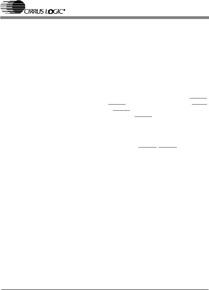
3.TYPICAL CONNECTION DIAGRAMS
Six typical connection diagrams have been presented to illustrate using the part with the different communication modes available. They are as follows:
Figure 13, "I2C® Control" on page 26
Figure 14, "I2C® Control with External Memory" on page 27
Figure 15, "SPI Control" on page 28
Figure 16, "SPI Control with External Memory" on page 29
Figure 17, "Intel® Parallel Control Mode" on page 30
Figure 18, "Motorola® Parallel Control Mode" on page 31
The following should be noted when viewing the typical connection diagrams:
The pins are grouped functionally in each of the typical connection diagrams. Please be aware that the CS493XX symbol may appear differently in each diagram.
The external memory interface is only supported when a serial communication mode has been chosen.
The typical connection diagrams demonstrate the PLL being used (CLKSEL is pulled low). To use CLKIN as the DSP clock, CLKSEL should be pulled high. The system designer must be aware that certain software features may not be available if external CLKIN is used as the DSP must run slower when external CLKIN is used. The system designer should also be aware of additional duty cycle requirements when using external CLKIN as a DSP clock. It is highly suggested that the system designer use the PLL and pull CLKSEL low.
3.1. Multiplexed Pins
The CS493XX family of digital signal processors (DSPs) incorporate a large amount of flexibility into a 44 pin package. Because of the high degree
CS49300 Family DSP
of integration, many of these pins are internally multiplexed to serve multiple purposes. Some pins are designed to operate in one mode at power up, and serve a different purpose when the DSP is running. Other pins have functionality which can be controlled by the application running on the DSP. In order to better explain the behavior of the part, the pins which are multiplexed have been given multiple names. Each name is specific to the pin’s operation in a particular mode.
An example of this would be the use of pin 20 in one of the serial control modes. During the boot period of the CS493XX, pin 20 is called ABOOT. ABOOT is sampled on the rising edge of RESET. If ABOOT is high the host must download code to the DSP. If ABOOT is low when sampled, the CS493XX goes into autoboot mode and loads itself with code by generating addresses and reading data on EMAD[7:0]. When the part has been loaded with code and is running an application, however, pin 20 is called INTREQ. INTREQ is an open drain output used to inform the host that the DSP has an outgoing message which should be read.
In this document, pins will be referred to by their functionality. Section 12, “Pin Descriptions” on page 80 describes each pin of the CS493XX and lists all of its names. Please refer to this section when exact pin numbers are in question.
The part has 12 general purpose input and output (GPIO[11:0]) pins that all have multiple functionality. While in one of the parallel communication modes (Section 6.2, “Parallel Host Communication” on page 41), these pins are used to implement the parallel host communication interface. While in one of the serial host modes these pins are used to implement an external memory interface. Alternatively while in one of the serial host modes these pins could be used for another general purpose if the application code has been programmed to support the special purpose. In this document the pins are referenced by the
24 |
DS339PP4 |

name corresponding to their particular use. Sometimes GPIO[11:0], or some subset thereof, is used when referring to the pins in a general sense.
3.2. Termination Requirements
The CS493XX incorporates open drain pins which must be pulled high for proper operation. INTREQ (pin 20) is always an open drain pin which requires a pull-up for proper operation. When in the I2C serial communication mode, the SCDIO signal (pin 19) is open drain and thus requires a pull-up for proper operation.
Due to the internal, multiplexed design of the pins, certain signals may or may not require termination depending on the mode being used. If a parallel host communication mode is not being used, GPIO[11:0] must be terminated or driven as these pins will come up as high impedance inputs and will be prone to oscillation if they are left floating. The specific termination requirements may vary since the state of some of the GPIO pins will determine the communication mode at the rising edge of reset (please see Section 6, “Control” on page 32 for more information). For the explicit termination requirements of each communication mode please see the typical connection diagrams.
Generally a 4.7k Ohm resistor is recommended for open drain pins. The communication mode setting pins (please see Section 6, “Control” on page 32 for more information) should also be terminated with a 4.7k resistor. A 10k Ohm resistor is sufficient for the GPIO pins and unused inputs.
3.3. Phase Locked Loop Filter
The internal phase locked loop (PLL) of the CS493XX requires an external filter for successful operation. The topology of this filter is shown in the typical connection diagrams. The component values are shown below. Care should be taken when laying out the filter circuitry to minimize trace lengths and to avoid any close routing of high frequency signals. Any noise coupled on to the
CS49300 Family DSP
filter circuit will be directly coupled into the PLL, which could affect performance.
Reference Designator |
Value |
|
|
C1 |
2.2uF |
|
|
C2 |
220pF |
|
|
C3 |
10nF |
|
|
R1 |
200k Ohm |
|
|
Table 1. PLL Filter Component Values
4.POWER
The CS493XX requires a 2.5V digital power supply for the digital logic within the DSP and a 2.5V analog power supply for the internal PLL. There are three digital power pins, VD1, VD2 and VD3, along with three digital grounds, DGND1, DGND2 and DGND3. There is one analog power pin, VA and one analog ground, AGND. The DSP will perform at its best when noise has been eliminated from the power supply. The recommendations given below for decoupling and power conditioning of the CS493XX will help to ensure reliable performance.
4.1. Decoupling
It is good practice to decouple noise from the power supply by placing capacitors directly between the power and ground of the CS493XX. Each pair of power pins (VD1/DGND, VD2/DGND, VD3/DGND, VA/AGND) should have its own decoupling capacitors. The recommended procedure is to place both a 0.1uF and a 1uF capacitor as close as physically possible to each power pin. The 0.1uF capacitor should be closest to the part (typically 5mm or closer).
4.2. Analog Power Conditioning
In order to obtain the best performance from the CS493XX’s internal PLL, the analog power supply (VA) must be as clean as possible. A ferrite bead should be used to filter the 2.5V power supply for the analog portion of the CS493XX. This power
DS339PP4 |
25 |
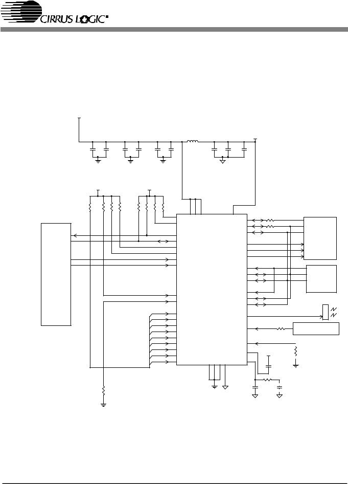
CS49300 Family DSP
+2.5 Supply (+2.5VD)
NOTE: A capacitor pair (1 uF and 0.1 uF) must be supplied for each power pin.
NOTE: +2.5VA is simply +2.5VD after filtering through the ferrite bead. Pin 32 must be referenced to +2.5VA
ROLLER |
INTERFACE |
NT |
I2C |
MICROCO |
|
|
|
|
|
|
|
|
|
|
FERRITE BEAD |
|
|
|
|
+2.5VA |
|
|
|||
|
+ 1 uF |
0.1 uF |
+ 1 uF |
0.1 uF |
+ 1 uF |
0.1 uF |
|
|
+ 1 uF |
0.1 uF + 47 uF |
|
|
|
||||||
|
+2.5VD |
|
|
|
+2.5VD |
|
|
|
|
|
|
|
|
|
|
|
|
|
|
Pack 10k |
3 . 3 k |
10k |
10k |
3 . 3 k |
3 . 3k |
4 . 7 k |
4 . 7 k |
|
23 |
12 |
1 |
|
|
34 |
|
|
|
|
|
Resistor |
|
|
|
|
|
|
|
37 |
VD 3 |
VD 2 |
VD 1 |
|
|
V A |
MCLK |
|
33 |
|
|
|
|
|
|
|
|
|
|
|
DD |
|
|
|
|
|
|
44 |
|
|
|
|
|
|
|
|
|
|
|
38 |
|
|
|
|
|
|
|
|
|
|
|
|
|
|
|
|
|
|
|
DC |
|
|
|
|
|
|
43 |
33 |
|
|
|
|
|
|
|
|
|
|
|
|
|
|
|
|
|
SCLK |
|
|
|||
|
|
|
|
|
|
|
|
|
|
|
|
|
|
|
|
|
|
||
|
|
|
|
|
|
|
|
|
|
|
|
|
|
|
|
|
|
|
|
|
|
|
|
|
|
|
|
|
|
|
|
|
|
|
LRCLK |
42 |
|
|
DAC (S) |
|
|
|
|
|
|
|
|
20 |
|
|
|
|
|
|
|
|
|
||
|
|
|
|
|
|
|
|
INTREQ |
|
|
|
|
|
|
|
|
|
||
|
|
|
|
|
|
|
|
19 |
SCDIO |
|
|
|
|
|
|
41 |
|
|
|
|
|
|
|
|
|
|
|
|
|
|
|
|
AUDATA0 |
|
|
|
|||
|
|
|
|
|
|
|
|
6 |
|
|
|
|
|
|
|
|
|||
|
|
|
|
|
|
|
|
SCDIN |
|
|
|
|
|
|
|
|
|||
|
|
|
|
|
|
|
|
|
|
|
|
|
|
|
|
|
|
||
|
|
|
|
|
|
|
|
|
|
|
|
|
|
|
40 |
|
|
|
|
|
|
|
|
|
|
|
|
18 |
|
|
|
|
|
AUDATA1 |
|
|
|
||
|
|
|
|
|
|
|
|
CS |
|
|
|
|
|
|
|
|
|||
|
|
|
|
|
|
|
|
|
|
|
|
|
|
39 |
|
|
|
||
|
|
|
|
|
|
|
|
|
|
|
|
|
AUDATA2 |
|
|
|
|||
|
|
|
|
|
|
|
|
7 |
|
|
|
|
|
|
|
|
|||
|
|
|
|
|
|
|
|
SCCLK |
|
|
|
|
|
|
|
|
|||
|
|
|
|
|
|
|
|
|
|
|
|
|
|
|
|
|
|
||
|
|
|
|
|
|
|
|
|
|
|
|
|
|
|
|
|
|
|
|
|
|
|
|
|
|
|
|
36 |
RESET |
|
|
|
|
|
|
27 |
|
|
|
|
|
|
|
|
|
|
|
|
|
|
|
|
|
CMPDAT |
|
|
|
||
|
|
|
|
|
|
|
|
|
|
|
|
|
|
|
|
|
|
||
|
|
|
|
|
|
|
|
|
|
|
|
|
|
|
|
|
|
|
|
|
|
|
|
|
|
|
|
|
|
|
CS493XX |
|
CMPCLK |
28 |
|
|
DIR or |
||
|
|
|
|
|
|
|
|
|
|
|
|
|
|
|
|||||
|
|
|
|
|
|
|
|
|
|
|
|
CMPREQ |
29 |
|
|
ADC [S] |
|||
|
|
|
|
|
|
|
|
|
|
|
|
|
|
|
|
|
|
|
|
|
|
|
|
|
|
|
|
|
|
|
|
|
|
|
SDATAN |
22 |
|
|
|
|
|
|
|
|
|
|
|
4 |
|
|
|
|
|
|
|
|
|
|
|
|
|
|
|
|
|
|
|
WR__GPIO10 |
|
|
|
|
|
|
25 |
|
|
|
|
|
|
|
|
|
|
|
|
|
|
|
|
|
|
SCLKN |
|
|
|
||
|
|
|
|
|
|
|
|
5 |
|
|
|
|
|
|
|
|
OPT_TX |
||
|
|
|
|
|
|
|
|
RD__GPIO11 |
|
|
|
|
|
|
|
|
|||
|
|
|
|
|
|
|
|
|
|
|
|
SLRCLKN |
26 |
|
|
||||
|
|
|
|
|
|
|
|
|
|
|
|
|
|
|
|
|
|||
|
|
|
|
|
|
|
|
|
|
|
|
|
|
|
|
|
|
||
|
|
|
|
|
|
|
|
21 |
GPIO8 |
|
|
|
|
|
|
3 |
|
|
|
|
|
|
|
|
|
|
|
|
|
|
|
|
|
XMT958 |
|
|
|
||
|
|
|
|
|
|
|
|
8 |
|
|
|
|
|
|
|
|
|
||
|
|
|
|
|
|
|
|
GPIO7 |
|
|
|
|
|
|
|
|
|
||
|
|
|
|
|
|
|
|
|
|
|
|
|
|
|
|
|
|
||
|
|
|
|
|
|
|
|
|
|
|
|
|
|
|
|
|
|
|
|
|
|
|
|
|
|
|
|
9 |
GPIO6 |
|
|
|
|
|
|
30 |
|
|
33 |
|
|
|
|
|
|
|
|
|
|
|
|
|
|
|
|
|
|||
|
|
|
|
|
|
|
|
10 |
GPIO5 |
|
|
|
|
|
CLKIN |
|
|
OSCILLATOR |
|
|
|
|
|
|
|
|
|
|
|
|
|
|
|
|
|
||||
|
|
|
|
|
|
|
|
|
|
|
|
|
|
|
|
|
|
|
|
|
|
|
|
|
|
|
|
11 |
GPIO4 |
|
|
|
|
|
|
|
|
|
|
|
|
|
|
|
|
|
|
|
|
|
|
|
|
|
|
|
|
|
|
|
|
|
|
|
|
|
|
14 |
GPIO3 |
|
|
|
|
|
CLKSEL |
31 |
|
|
|
|
|
|
|
|
|
|
|
|
|
|
|
|
|
|
|
|
|
||
|
|
|
|
|
|
|
|
15 |
GPIO2 |
|
|
|
|
|
|
32 |
+2.5VA |
10k |
|
|
|
|
|
|
|
|
|
16 |
|
1D |
2D |
3D |
D |
FLT2 |
|||||
|
|
|
|
|
|
|
|
GPIO1 |
|
||||||||||
|
|
|
|
|
|
|
|
|
|
|
|
|
|
|
|
|
|
|
|
|
|
|
EMAD_GPIO [8:0] |
|
|
17 |
GPIO0 |
|
D G N |
D G N |
D G N |
A G N |
FLT1 |
33 |
+ |
C1 |
|
||
|
|
|
|
|
|
|
|
|
|
|
|
|
|
|
|||||
|
|
|
|
|
|
|
|
|
13 |
24 |
35 |
|
|
|
|
|
|||
|
|
|
|
|
|
|
|
|
|
|
2 |
|
|
|
|
|
|||
|
|
|
|
|
|
|
|
|
|
|
|
|
|
|
|
|
R1 |
|
|
|
3 . 3k |
|
|
|
|
|
|
|
|
|
|
|
|
|
|
C2 |
|
|
C3 |
|
|
|
|
|
|
|
|
|
|
|
|
|
|
|
|
|
|
|
|
|
|
|
|
|
Figure 13. I2C® Control |
|
|
|
|
|
|
|
|
||||||
26 |
DS339PP4 |
Loading...