


 Loading...
Cirrus Logic CS5102A-KP, CS5102A-KL, CS5102A-JP, CS5101A-KP8, CS5101A-KL8 Datasheet
...
|
|
|
|
|
|
CS5101A |
|
|
|
|
|
|
|
CS5102A |
|
|
|
|
|
|
|||
|
|
|
|
|
|||
|
|
|
|||||
|
|
|
|
|
|
|
|
|
16-Bit, 100 kHz / 20 kHz A/D Converters |
||||||
|
|
|
|||||
Features |
Description |
||||||
λMonolithic CMOS A/D Converters |
The CS5101A and CS5102A are 16-bit monolithic |
||||||
- |
Inherent Sampling Architecture |
CMOS analog-to-digital converters capable of 100 kHz |
|||||
(5101A) and 20 kHz (5102A) throughput. The |
|||||||
- |
2-Channel Input Multiplexer |
||||||
CS5102A’s low power consumption of 44 mW, coupled |
|||||||
- |
Flexible Serial Output Port |
||||||
with a power down mode, makes it particularly suitable |
|||||||
λUltra-Low Distortion |
for battery powered operation. |
||||||
- |
S/(N+D): 92 dB |
On-chip self-calibration circuitry achieves nonlinearity of |
|||||
- |
THD: 0.001% |
±0.001% of FS and guarantees 16-bit no missing codes |
|||||
λConversion Time |
over the entire specified temperature range. Superior lin- |
||||||
- |
CS5101A: 8 µs |
earity also leads to 92 dB S/(N+D) with harmonics below |
|||||
-100 dB. Offset and full-scale errors are minimized dur- |
|||||||
- |
CS5102A: 40 µs |
||||||
ing the calibration cycle, eliminating the need for external |
|||||||
λLinearity Error: ±0.001% FS |
trimming. |
||||||
- Guaranteed No Missing Codes |
The CS5101A and CS5102A each consist of a 2-chan- |
||||||
λSelf-Calibration Maintains Accuracy |
nel input multiplexer, DAC, conversion and calibration |
||||||
- Over Time and Temperature |
microcontroller, clock generator, comparator, and serial |
||||||
λLow Power Consumption |
communications port. The inherent sampling architec- |
||||||
ture of the device eliminates the need for an external |
|||||||
- |
CS5101A: 320 mW |
||||||
track and hold amplifier. |
|||||||
- |
CS5102A: 44 mW |
The converters' 16-bit data is output in serial form with ei- |
|||||
- Power-down Mode: <1 mW |
|||||||
ther binary or 2's complement coding. Three output |
|||||||
λEvaluation Board Available |
timing modes are available for easy interfacing to micro- |
||||||
|
|
|
|
|
controllers and shift registers. Unipolar and bipolar input |
||
|
|
|
|
|
ranges are digitally selectable. |
||
|
|
|
|
|
|
ORDERING INFORMATION |
|||||
|
|
|
|
|
|
|
See page 36. |
|
|
||
I |
|
|
|
|
|
|
|
|
|
|
|
|
HOLD SLEEPRST STBY CODE BP/UP CRS/FIN TRK1 TRK2 SSH/SDLSDATA |
||||||||||
|
12 |
28 |
2 |
5 |
16 |
17 |
10 |
8 |
9 |
11 |
15 |
CLKIN |
3 |
|
|
|
|
|
|
|
|
|
14 |
4 |
Clock |
|
Control |
|
|
|
|
SCLK |
|||
XOUT |
|
|
|
|
|
||||||
Generator |
|
|
|
|
|
|
|||||
|
|
|
|
|
|
|
|
|
|||
REFBUF |
21 |
|
|
|
Calibration |
|
Microcontroller |
|
|||
|
|
|
|
|
|
|
|||||
|
|
- |
|
|
|
SRAM |
|
|
|||
|
20 |
|
|
|
|
|
|
|
|
||
|
|
|
|
|
|
|
|
|
|
||
VREF |
+ |
|
|
|
|
|
|
|
|
26 |
|
|
|
|
|
|
|
|
|
|
|||
|
|
|
|
|
|
|
|
|
|
|
TEST |
AIN1 |
19 |
- |
|
|
|
16-Bit Charge |
|
|
|
27 |
|
|
|
|
|
|
|
|
|||||
|
24 |
+ |
|
|
|
Redistribution |
|
- |
|
SCKMOD |
|
AIN2 |
|
|
|
DAC |
|
|
+ |
|
|
||
|
|
|
|
|
|
|
|
||||
|
|
|
|
|
|
|
|
18 |
|||
|
13 |
|
|
|
|
|
|
|
Comparator |
||
CH1/2 |
- |
|
|
|
|
|
|
OUTMOD |
|||
|
|
|
|
|
|
|
|
|
|
||
|
22 |
+ |
|
|
|
|
|
|
|
|
|
AGND |
|
|
|
|
|
|
|
|
|
|
|
|
|
|
|
|
|
|
|
|
|
|
|
|
|
25 |
|
23 |
|
6 |
1 |
|
7 |
|
|
|
|
VA+ |
|
VA- |
|
DGND |
VD- |
|
VD+ |
|
|
Cirrus Logic, Inc. |
Copyright ã Cirrus Logic, Inc. 1997 |
|
Crystal Semiconductor Products Division |
MAR ‘95 |
|
P.O. Box 17847, Austin, Texas 78760 |
(All Rights Reserved) |
DS45F2 |
|
(512) 445 7222 FAX: (512) 445 7581 |
1 |
|
http://www.crystal.com |
||
|

CS5101A
ANALOG CHARACTERISTICS (TA = TMIN to TMAX; VA+, VD+ = 5V; VA-, VD- = -5V; VREF = 4.5V; Full-Scale Input Sinewave, 1 kHz; CLKIN = 4 MHz for -16, 8 MHz for -8; fs = 50 kHz for -16,
100 kHz for -8; Bipolar Mode; FRN Mode; AIN1 and AIN2 tied together, each channel tested separately; Analog Source Impedance = 50 Ω with 1000 pF to AGND unless otherwise specified)
|
|
|
CS5101A-J,K |
CS5101A-A,B |
|
|
|||||
Parameter* |
|
Min |
Typ |
Max |
Min |
Typ |
Max |
|
Units |
||
|
|
||||||||||
|
|
|
|
|
|
|
|
||||
Specified Temperature Range |
|
0 to |
+70 |
|
-40 to +85 |
|
° |
||||
|
|
|
|
|
|
|
|
|
|
|
C |
Accuracy |
|
|
|
|
|
|
|
|
|
|
|
Linearity Error |
-J,A,S |
(Note 1) |
- |
0.002 |
0.003 |
- |
0.002 |
0.003 |
|
%FS |
|
|
-K,B,T |
|
- |
0.001 |
0.002 |
- |
0.001 |
0.002 |
|
%FS |
|
|
Drift |
(Note 2) |
- |
± 1/4 |
- |
- |
± 1/4 |
- |
|
LSB |
|
Differential Linearity |
|
(Notes 3, 4) |
16 |
- |
|
- |
16 |
- |
- |
|
Bits |
Full Scale Error |
-J,A,S |
(Note 1) |
- |
± |
1 |
± 4 |
- |
± 1 |
± 4 |
|
LSB |
|
-K,B,T |
|
- |
± |
1 |
± 3 |
- |
± 1 |
± 3 |
|
LSB |
|
Drift |
(Note 2) |
- |
± |
1 |
- |
- |
± 1 |
- |
|
LSB |
Unipolar Offset |
-J,A,S |
(Note 1) |
- |
± 2 |
± 5 |
- |
± 2 |
± 5 |
|
LSB |
|
|
-K,B,T |
|
- |
± 2 |
± 4 |
- |
± 2 |
± 4 |
|
LSB |
|
|
Drift |
(Note 2) |
- |
± |
1 |
- |
- |
± 1 |
- |
|
LSB |
Bipolar Offset |
-J,A,S |
(Note 1) |
- |
± 2 |
± 5 |
- |
± 2 |
± 5 |
|
LSB |
|
|
-K,B,T |
|
- |
± 2 |
± 3 |
- |
± 2 |
± 3 |
|
LSB |
|
|
Drift |
(Note 2) |
- |
± |
1 |
- |
- |
± 2 |
- |
|
LSB |
Bipolar Negative Full-Scale Error |
|
|
|
|
|
|
|
|
|
||
|
-J,A,S |
(Note 1) |
- |
± |
1 |
± 4 |
- |
± 1 |
± 4 |
|
LSB |
|
-K,B,T |
|
- |
± |
1 |
± 3 |
- |
± 1 |
± 3 |
|
LSB |
|
Drift |
(Note 2) |
- |
± |
1 |
- |
- |
± 1 |
- |
|
LSB |
|
|
|
|
|
|
|
|||||
Dynamic Performance (Bipolar Mode) |
|
|
|
|
|
|
|
|
|
||
Peak Harmonic or Spurious Noise (Note 1) |
|
|
|
|
|
|
|
|
|
||
1 kHz Input |
-J,A,S |
|
96 |
100 |
- |
96 |
100 |
- |
|
dB |
|
|
-K,B,T |
|
98 |
102 |
- |
98 |
102 |
- |
|
dB |
|
12 kHz Input |
-J,A,S |
|
85 |
88 |
- |
85 |
88 |
- |
|
dB |
|
|
-K,B,T |
|
85 |
91 |
- |
85 |
91 |
- |
|
dB |
|
Total Harmonic Distortion -J,A,S |
- |
0.002 |
- |
- |
0.002 |
- |
|
% |
|||
|
-K,B,T |
|
- |
0.001 |
- |
- |
0.001 |
- |
|
% |
|
Signal-to-Noise Ratio |
|
(Note 1) |
|
|
|
|
|
|
|
|
|
0dB Input |
-J,A,S |
|
87 |
90 |
- |
87 |
90 |
- |
|
dB |
|
|
-K,B,T |
|
90 |
92 |
- |
90 |
92 |
- |
|
dB |
|
-60 dB Input |
-J,A,S |
|
- |
30 |
- |
- |
30 |
- |
|
dB |
|
|
-K,B,T |
|
- |
32 |
- |
- |
32 |
- |
|
dB |
|
Noise |
|
(Note 5) |
|
|
|
|
|
|
|
|
|
|
Unipolar Mode |
- |
35 |
- |
- |
35 |
- |
|
μVrms |
||
|
Bipolar Mode |
- |
70 |
- |
- |
70 |
- |
|
μVrms |
||
Notes: 1. Applies after calibration at any temperature within the specified temperature range. At temp
2.Total drift over specified temperature range after calibration at power-up at 25 °C.
3.Minimum resolution for which no missing codes is guaranteed over the specified temperature range.
4.Clock speeds of less than 1.0 MHz, at temperatures >100°C will degrade DNL performance.
5.Wideband noise aliased into the baseband. Referred to the input.
*Refer to Parameter Definitions (immediately following the pin descriptions at the end of this data sheet).
Specifications are subject to change without notice.
2 |
DS45F2 |

|
|
|
|
|
|
|
|
|
|
|
|
|
|
|
|
|
|
|
CS5101A |
|
|
|
|
|
|
|
|
|
|
|
|
|
|
|
|
|
|
|
|
|
|
||
|
|
|
|
|
|
|
|
|
|
|
|
|
|
|
|
|
|
|
|||
|
|
|
|
|
|
|
|
|
|
|
|
|
|
|
|
|
|
|
|
|
|
|
|
|
|
|
|
|
|
|
|
|
|
|
|
|
|
|
|
|
|
|
|
ANALOG CHARACTERISTICS (continued) |
|
|
|
|
|
|
|
|
|||||||||||||
|
|
|
|
|
|
|
|
|
|
|
|
|
|
|
|
|
|
||||
|
|
|
|
|
|
|
|
|
|
|
|
|
CS5101A -J,K |
CS5101A -A,B |
|
|
|
||||
|
|
|
|
|
|
Parameter* |
|
|
Symbol |
Min |
Typ |
Max |
Min |
Typ |
Max |
|
Units |
|
|||
|
|
|
|
|
|
|
|||||||||||||||
Specified Temperature Range |
- |
0 to +70 |
40 to +85 |
|
° |
|
|||||||||||||||
|
|
|
|
|
|
|
|
|
|
|
|
|
|
|
|
|
|
|
|
C |
|
Analog Input |
|
|
|
|
|
|
|
|
|
|
|
|
|
|
|
||||||
Aperture Time |
|
|
|
|
|
- |
- |
25 |
- |
- |
25 |
- |
|
ns |
|
||||||
Aperture Jitter |
|
|
|
|
|
- |
- |
100 |
- |
- |
100 |
- |
|
ps |
|
||||||
Input Capacitance |
|
|
|
|
(Note 6) |
|
|
|
|
|
|
|
|
|
|
||||||
|
|
|
|
|
|
|
Unipolar Mode |
- |
- |
320 |
425 |
- |
320 |
425 |
|
pF |
|
||||
|
|
|
|
|
|
|
Bipolar Mode |
- |
- |
200 |
265 |
- |
200 |
265 |
|
pF |
|
||||
Conversion & Throughput |
|
|
|
|
|
|
|
|
|
|
|||||||||||
Conversion Time |
|
|
|
|
(Note 7) |
|
|
|
|
|
|
|
|
|
|
||||||
|
|
|
|
|
|
|
|
|
|
-8 |
tc |
- |
- |
8.12 |
- |
- |
8.12 |
|
μ |
|
|
|
|
|
|
|
|
|
|
|
|
-16 |
|
- |
- |
16.25 |
- |
- |
16.25 |
|
s |
|
|
|
|
|
|
|
|
|
|
|
|
tc |
|
μs |
|
||||||||
Acquisition Time |
|
|
|
|
(Note 8) |
|
|
|
|
|
|
|
|
|
|
||||||
|
|
|
|
|
|
|
|
|
|
-8 |
ta |
- |
- |
1.88 |
- |
- |
1.88 |
|
μ |
|
|
|
|
|
|
|
|
|
|
|
|
-16 |
|
- |
2.6 |
3.75 |
- |
2.6 |
3.75 |
|
s |
|
|
|
|
|
|
|
|
|
|
|
|
ta |
|
μs |
|
||||||||
Throughput |
|
|
|
|
(Note 9) |
|
|
|
|
|
|
|
|
|
|
||||||
|
|
|
|
|
|
|
|
|
|
-8 |
ftp |
100 |
- |
- |
100 |
- |
- |
|
kHz |
|
|
|
|
|
|
|
|
|
|
|
|
-16 |
ftp |
50 |
- |
- |
50 |
- |
- |
|
kHz |
|
|
Power Supplies |
|
|
|
|
|
|
|
|
|
|
|
|
|
|
|
||||||
Power Supply Current |
|
(Note 10) |
|
|
|
|
|
|
|
|
|
|
|||||||||
|
|
|
|
|
|
|
Positive Analog |
IA+ |
- |
21 |
28 |
- |
21 |
28 |
|
mA |
|
||||
|
|
|
|
|
|
|
Negative Analog |
IA- |
- |
-21 |
-28 |
- |
-21 |
-28 |
|
mA |
|
||||
(SLEEP High) |
Positive Digital |
ID+ |
- |
11 |
15 |
- |
11 |
15 |
|
mA |
|
||||||||||
|
|
|
|
|
|
|
Negative Digital |
ID- |
- |
-11 |
-15 |
- |
-11 |
-15 |
|
mA |
|
||||
Power Consumption |
|
|
|
(Notes 10, 11) |
|
|
|
|
|
|
|
|
|
|
|||||||
|
|
|
|
|
|
|
(SLEEP High) |
Pdo |
- |
320 |
430 |
- |
320 |
430 |
|
mW |
|
||||
|
|
|
|
|
|
|
(SLEEP Low) |
Pds |
- |
1 |
- |
- |
1 |
- |
|
mW |
|
||||
Power Supply Rejection: |
|
(Note 12) |
|
|
|
|
|
|
|
|
|
|
|||||||||
|
|
|
|
|
|
|
|
Positive Supplies |
PSR |
- |
84 |
- |
- |
84 |
- |
|
dB |
|
|||
|
|
|
|
|
|
|
Negative Supplies |
PSR |
- |
84 |
- |
- |
84 |
- |
|
dB |
|
||||
Notes: 6. Applies only in the track mode. When converting or calibrating, input capacitance will not exceed |
30 pF. |
|
|||||||||||||||||||
7.Conversion time scales directly to the master clock speed. The times shown are for synchronous, internal loopback (FRN mode) with 8.0 MHz CLKIN. In PDT, RBT, and SSC modes, asynchronous delay between the falling edge of HOLD and the start of conversion may add to the apparent conversion time. This delay will not exceed 1.5 master clock cycles + 10 ns. In PDT, RBT, and SSC modes, CLKIN can be increased as long as the HOLD sample rate is 100 kHz max.
8.The CS5101A requires 6 clock cycles of coarse charge, followed by a minimum of 1.125 μs of fine charge. FRN mode allows 9 clock cycles for fine charge which provides for the minimum 1.125 μs with an 8 MHz
clock, however; in PDT, RBT, or SSC modes, at clock frequencies of 8 MHz or less, fine charge may be less than 9 clock cycles. This reflects the typ. specification (6 clock cycles + 1.125 μs).
9.Throughput is the sum of the acquisition and conversion times. It will vary in accordance with conditions affecting acquisition and conversion times, as described above.
10.All outputs unloaded. All inputs at VD+ or DGND.
11.Power consumption in the sleep mode applies with no master clock applied (CLKIN held high or low).
12.With 300 mV p-p, 1 kHz ripple applied to each supply separately in the bipolar mode. Rejection improves by 6 dB in the unipolar mode to 90 dB. Figure 23 shows a plot of typical power supply rejection versus frequency.
DS45F2 |
3 |

CS5101A
SWITCHING CHARACTERISTICS (TA = TMIN to TMAX; VA+, VD+ = 5V ± 10%;
VA-, VD- = -5V ± 10%; Inputs: Logic 0 = 0V, Logic 1 = VD+; CL = 50 pF)
Parameter |
|
Symbol |
Min |
Typ |
Max |
Units |
|
|
|
|
|
|
|
CLKIN Period |
(Note 4) |
|
|
|
|
|
|
-8 |
tclk |
108 |
- |
10,000 |
ns |
|
-16 |
tclk |
250 |
- |
10,000 |
ns |
CLKIN Low Time |
|
tclkl |
37.5 |
- |
- |
ns |
CLKIN High Time |
|
tclkh |
37.5 |
- |
- |
ns |
Crystal Frequency |
(Note 13) |
|
|
|
|
|
|
-8 |
fxtal |
2.0 |
- |
9.216 |
MHz |
|
-16 |
fxtal |
2.0 |
- |
4.0 |
MHz |
SLEEP Rising to Oscillator Stable |
(Note 14) |
- |
- |
2 |
- |
ms |
RST Pulse Width |
|
trst |
150 |
- |
- |
ns |
RST to STBY Falling |
|
tdrrs |
- |
100 |
- |
ns |
RST Rising to STBY Rising |
|
tcal |
- |
11,528,160 |
- |
tclk |
CH1/2 Edge to TRK1, TRK2 Rising |
(Note 15) |
tdrsh1 |
- |
80 |
- |
ns |
CH1/2 Edge to TRK1, TRK2 Falling |
(Note 15) |
tdfsh4 |
- |
- |
68tclk+260 |
ns |
HOLD to SSH Falling |
(Note 16) |
tdfsh2 |
- |
60 |
|
ns |
HOLD to TRK1, TRK2, Falling |
(Note 16) |
tdfsh1 |
66tclk |
- |
68tclk+260 |
ns |
HOLD to TRK1, TRK2, SSH Rising |
(Note 16) |
tdrsh |
- |
120 |
- |
ns |
HOLD Pulse Width |
(Note 17) |
thold |
1tclk+20 |
- |
63tclk |
ns |
HOLD to CH1/2 Edge |
(Note 16) |
tdhlri |
15 |
- |
64tclk |
ns |
HOLD Falling to CLKIN Falling |
(Note 17) |
thcf |
95 |
- |
1tclk+10 |
ns |
Notes: 13. External loading capacitors are required to allow the crystal to oscillate. Maximum crystal frequency is 8.0 MHz in FRN mode (100 kHz sample rate).
14.With a 8 MHz crystal, two 10 pF loading capacitors and a 10 MΩ parallel resistor (see Figure 8).
15.These times are for FRN mode.
16.SSH only works correctly if HOLD falling edge is within +15 to +30 ns of CH1/2 edge or if CH1/2 edge occurs after HOLD rises to 64 tclk after HOLD has fallen. These times are for PDT and RBT modes.
17.When HOLD goes low, the analog sample is captured immediately. To start conversion, HOLD must be latched by a falling edge of CLKIN. Conversion will begin on the next rising edge of CLKIN after HOLD is latched. If HOLD is operated synchronous to CLKIN, the HOLD pulse width may be as narrow as 150 ns for all CLKIN frequencies if CLKIN falls 95 ns after HOLD falls. This
ensures that the HOLD pulse will meet the minimum specification for thcf.
4 |
DS45F2 |

CS5102A
ANALOG CHARACTERISTICS (TA = TMIN to TMAX; VA+, VD+ = 5V; VA-, VD- = -5V; VREF = 4.5V; Full-Scale Input Sinewave, 200 Hz; CLKIN = 1.6 MHz; fs = 20 kHz; Bipolar Mode; FRN Mode;
AIN1 and AIN2 tied together, each channel tested separately; Analog Source Impedance = 50 Ω with 1000pF to AGND unless otherwise specified)
|
|
|
CS5102A-J,K |
CS5102A-A,B |
|
|
|||||
Parameter* |
|
Min |
Typ |
Max |
Min |
Typ |
Max |
|
Units |
||
|
|
||||||||||
|
|
|
|
|
|
|
|
||||
Specified Temperature Range |
|
0 to |
+70 |
|
-40 to +85 |
|
°C |
||||
|
|
|
|
|
|
|
|
|
|
|
|
Accuracy |
|
|
|
|
|
|
|
|
|
|
|
|
|
|
|
|
|
|
|
|
|
|
|
Linearity Error |
-J,A,S |
(Note 1) |
- |
0.002 |
0.003 |
- |
0.002 |
0.003 |
|
%FS |
|
|
-K,B,T |
|
- |
0.001 0.0015 |
- |
0.001 0.0015 |
|
%FS |
|||
|
Drift |
(Note 2) |
- |
± 1/4 |
- |
- |
± 1/4 |
- |
|
LSB |
|
Differential Linearity |
|
(Notes 3, 18) |
16 |
- |
|
- |
16 |
- |
- |
|
Bits |
Full Scale Error |
-J,A,S |
(Note 1) |
- |
± |
2 |
± 4 |
- |
± 2 |
± 4 |
|
LSB |
|
-K,B,T |
|
- |
± |
2 |
± 3 |
- |
± 2 |
± 3 |
|
LSB |
|
Drift |
(Note 2) |
- |
± |
1 |
- |
- |
± 1 |
- |
|
LSB |
Unipolar Offset |
-J,A,S |
(Note 1) |
- |
± 1 |
± 4 |
- |
± 1 |
± 4 |
|
LSB |
|
|
-K,B,T |
|
- |
± 1 |
± 3 |
- |
± 1 |
± 3 |
|
LSB |
|
|
Drift |
(Note 2) |
- |
± |
1 |
- |
- |
± 1 |
- |
|
LSB |
Bipolar Offset |
-J,A,S |
(Note 1) |
- |
± 1 |
± 4 |
- |
± 1 |
± 4 |
|
LSB |
|
|
-K,B,T |
|
- |
± 1 |
± 3 |
- |
± 1 |
± 3 |
|
LSB |
|
|
Drift |
(Note 2) |
- |
± |
1 |
- |
- |
± 2 |
- |
|
LSB |
Bipolar Negative |
-J,A,S |
(Note 1) |
- |
± |
2 |
± 4 |
- |
± 2 |
± 4 |
|
LSB |
Full-Scale Error |
-K,B,T |
|
- |
± |
2 |
± 3 |
- |
± 2 |
± 3 |
|
LSB |
|
Drift |
(Note 2) |
- |
± |
1 |
- |
- |
± 2 |
- |
|
LSB |
Dynamic Performance (Bipolar Mode) |
|
|
|
|
|
|
|
|
|
||
Peak Harmonic or |
-J,A,S |
(Note 1) |
96 |
100 |
- |
96 |
100 |
- |
|
dB |
|
Spurious Noise |
-K,B,T |
|
98 |
102 |
- |
98 |
102 |
- |
|
dB |
|
Total Harmonic Distortion -J,A,S |
- |
0.002 |
- |
- |
0.002 |
- |
|
% |
|||
|
-K,B,T |
|
- |
0.001 |
- |
- |
0.001 |
- |
|
% |
|
|
|
|
|
|
|
|
|
|
|
|
|
Signal-to-Noise Ratio |
|
(Note 1) |
|
|
|
|
|
|
|
|
|
0dB Input |
-J,A,S |
|
87 |
90 |
- |
87 |
90 |
- |
|
dB |
|
|
-K,B,T |
|
90 |
92 |
- |
90 |
92 |
- |
|
dB |
|
-60 dB Input |
-J,A,S |
|
- |
30 |
- |
- |
30 |
- |
|
dB |
|
|
-K,B,T |
|
- |
32 |
- |
- |
32 |
- |
|
dB |
|
|
|
|
|
|
|
|
|
|
|
|
|
Noise |
|
(Note 5) |
|
|
|
|
|
|
|
|
μVrms |
|
Unipolar Mode |
- |
35 |
- |
- |
35 |
- |
|
|||
|
Bipolar Mode |
- |
70 |
- |
- |
70 |
- |
|
μVrms |
||
Note: 18. Clock speeds of less than 1.6 MHz, at temperatures >100°C will degrade DNL performance.
*Refer to Parameter Definitions (immediately following the pin descriptions at the end of this data sheet).
Specifications are subject to change without notice.
DS45F2 |
5 |

|
|
|
|
|
|
|
|
|
|
|
|
|
|
|
|
|
|
|
CS5102A |
|
|
|
|
|
|
|
|
|
|
|
|
|
|
|
|
|
|
|
|
|
|
||
|
|
|
|
|
|
|
|
|
|
|
|
|
|
|
|
|
|
|
|
||
|
|
|
|
|
|
|
|
|
|
|
|
|
|
|
|
|
|
|
|
|
|
|
|
|
|
|
|
|
|
|
|
|
|
|
|
|
|
|
|
|
|
||
ANALOG CHARACTERISTICS (continued) |
|
|
|
|
|
|
|
||||||||||||||
|
|
|
|
|
|
|
|
|
|
|
|
|
|
|
|
|
|
||||
|
|
|
|
|
|
|
|
|
|
|
|
|
CS5102A -J,K |
CS5102A -A,B |
|
|
|
||||
|
|
|
|
|
|
Parameter* |
|
|
Symbol |
Min |
Typ |
Max |
Min |
Typ |
Max |
|
Units |
|
|||
|
|
|
|
|
|
|
|
||||||||||||||
Specified Temperature Range |
- |
|
0 to +70 |
40 to +85 |
|
° |
|
||||||||||||||
|
|
|
|
|
|
|
|
|
|
|
|
|
|
|
|
|
|
|
|
C |
|
Analog Input |
|
|
|
|
|
|
|
|
|
|
|
|
|
|
|
||||||
|
|
|
|
|
|
|
|
|
|
|
|
|
|
|
|
||||||
Aperture Time |
|
|
|
|
|
- |
- |
30 |
- |
- |
30 |
- |
|
ns |
|
||||||
|
|
|
|
|
|
|
|
|
|
|
|
|
|
|
|
||||||
Aperture Jitter |
|
|
|
|
|
- |
- |
100 |
- |
- |
100 |
- |
|
ps |
|
||||||
|
|
|
|
|
|
|
|
|
|
|
|
|
|
|
|
||||||
Input Capacitance |
|
|
|
|
(Note 6) |
- |
- |
320 |
425 |
- |
320 |
425 |
|
pF |
|
||||||
|
|
|
|
|
|
|
Unipolar Mode |
- |
- |
200 |
265 |
- |
200 |
265 |
|
pF |
|
||||
|
|
|
|
|
|
|
Bipolar Mode |
|
|
|
|
|
|
|
|
|
|
||||
|
|
|
|
|
|
|
|
|
|
|
|||||||||||
Conversion & Throughput |
|
|
|
|
|
|
|
|
|
|
|||||||||||
|
|
|
|
|
|
|
|
|
|
|
|
|
|
|
|
||||||
Conversion Time |
|
|
|
|
(Note 19) |
tc |
- |
- |
40.625 |
- |
- |
40.625 |
|
μs |
|
||||||
Acquisition Time |
|
|
|
|
(Note 20) |
ta |
- |
- |
9.375 |
- |
- |
9.375 |
|
μs |
|
||||||
|
|
|
|
|
|
|
|
|
|
|
|
|
|
|
|
||||||
Throughput |
|
|
|
|
(Note 21) |
ftp |
20 |
- |
- |
20 |
- |
- |
|
kHz |
|
||||||
Power Supplies |
|
|
|
|
|
|
|
|
|
|
|
|
|
|
|
||||||
|
|
|
|
|
|
|
|
|
|
|
|
|
|||||||||
Power Supply Current |
|
(Note 22) |
|
|
|
|
|
|
|
|
|
|
|||||||||
|
|
|
|
|
|
|
Positive Analog |
IA+ |
- |
2.4 |
3.5 |
- |
2.4 |
3.5 |
|
mA |
|
||||
|
|
|
|
|
|
|
Negative Analog |
IA- |
- |
-2.4 |
-3.5 |
- |
-2.4 |
-3.5 |
|
mA |
|
||||
(SLEEP High) |
Positive Digital |
ID+ |
- |
2.5 |
3.5 |
- |
2.5 |
3.5 |
|
mA |
|
||||||||||
|
|
|
|
|
|
|
Negative Digital |
ID- |
- |
-1.5 |
-2.5 |
- |
-1.5 |
-2.5 |
|
mA |
|
||||
Power Consumption |
|
|
|
(Notes 11, 22) |
|
|
|
|
|
|
|
|
|
|
|||||||
|
|
|
|
|
|
|
(SLEEP High) |
Pdo |
- |
44 |
65 |
- |
44 |
65 |
|
mW |
|
||||
|
|
|
|
|
|
|
(SLEEP Low) |
Pds |
- |
1 |
- |
- |
1 |
- |
|
mW |
|
||||
Power Supply Rejection: |
|
(Note 23) |
|
|
|
|
|
|
|
|
|
|
|||||||||
|
|
|
|
|
|
|
Positive Supplies |
PSR |
- |
84 |
- |
- |
84 |
- |
|
dB |
|
||||
|
|
|
|
|
|
|
Negative Supplies |
PSR |
- |
84 |
- |
- |
84 |
- |
|
dB |
|
||||
|
|
|
|
|
|
|
|
|
|
|
|
|
|
|
|
|
|
|
|
|
|
Notes: 19. Conversion time scales directly to the master clock speed. The times shown are for synchronous, internal loopback (FRN mode). In PDT, RBT, and SSC modes, asynchronous delay between the falling edge of HOLD and the start of conversion may add to the apparent conversion time. This delay will not exceed 1 master clock cycle + 140 ns.
20.The CS5102A requires 6 clock cycles of coarse charge, followed by a minimum of 5.625 μs of fine charge. FRN mode allows 9 clock cycles for fine charge which provides for the minimum 5.625 μs with an 1.6 MHz clock, however; in PDT, RBT, or SSC modes, at clock frequencies less than 1.6 MHz, fine charge may
be less than 9 clock cycles.
21.Throughput is the sum of the acquisition and conversion times. It will vary in accordance with conditions affecting acquisition and conversion times, as described above.
22.All outputs unloaded. All inputs at VD+ or DGND. See table below for power dissipation vs. clock frequency.
23.With 300 mV p-p, 1 kHz ripple applied to each supply separately in the bipolar mode. Rejection improves by 6 dB in the unipolar mode to 90 dB. Figure 23 shows a plot of typical power supply rejection versus frequency.
Typ. Power (mW) |
CLKIN (MHz) |
34 |
0.8 |
37 |
1.0 |
39 |
1.2 |
41 |
1.4 |
44 |
1.6 |
6 |
DS45F2 |

CS5102A
SWITCHING CHARACTERISTICS (TA = TMIN to TMAX;
VA+, VD+ = 5V ± 10%; VA-, VD- = -5V ± 10%; Inputs: Logic 0 = 0V, Logic 1 = VD+; CL = 50 pF)
Parameter |
|
Symbol |
Min |
Typ |
Max |
Units |
|
|
|
|
|
|
|
CLKIN Period |
(Note 18,24) |
tclk |
0.5 |
- |
10 |
μs |
CLKIN Low Time |
|
tclkl |
200 |
- |
- |
ns |
CLKIN High Time |
|
tclkh |
200 |
- |
- |
ns |
Crystal Frequency |
(Note 24, 25) |
fxtal |
0.9 |
1.6 |
2.0 |
MHz |
SLEEP Rising to Oscillator Stable |
(Note 26) |
- |
- |
20 |
- |
ms |
RST Pulse Width |
|
trst |
150 |
- |
- |
ns |
RST to STBY Falling |
|
tdrrs |
- |
100 |
- |
ns |
RST Rising to STBY Rising |
|
tcal |
- |
2,882,040 |
- |
tclk |
CH1/2 Edge to TRK1, TRK2 Rising |
(Note 27) |
tdrsh1 |
- |
80 |
- |
ns |
CH1/2 Edge to TRK1, TRK2 Falling |
(Note 27) |
tdfsh4 |
- |
- |
68tclk+260 |
ns |
HOLD to SSH Falling |
(Note 28) |
tdfsh2 |
- |
60 |
|
ns |
HOLD to TRK1, TRK2, Falling |
(Note 28) |
tdfsh1 |
66tclk |
- |
68tclk+260 |
ns |
HOLD to TRK1, TRK2, SSH Rising |
(Note 28) |
tdrsh |
- |
120 |
- |
ns |
HOLD Pulse Width |
(Note 29) |
thold |
1tclk+20 |
- |
63tclk |
ns |
HOLD to CH1/2 Edge |
(Note 28) |
tdhlri |
15 |
- |
64tclk |
ns |
HOLD Falling to CLKIN Falling |
(Note 29) |
thcf |
55 |
- |
1tclk+10 |
ns |
Note: 24. Minimum CLKIN period is 0.625 μs in FRN mode (20 kHz sample rate). At temperatures >+85 °C, and with clock frequencies <1.6 MHz, analog performance may be degraded.
25.External loading capacitors are required to allow the crystal to oscillate. Maximum crystal frequency is 1.6 MHz in FRN mode (20 kHz sample rate).
26.With a 2.0 MHz crystal, two 33 pF loading capacitors and a 10 MΩ parallel resistor (see Figure 8).
27.These times are for FRN mode.
28.SSH only works correctly if HOLD falling edge is within +15 to +30 ns of CH1/2 edge or if CH1/2 edge occurs after HOLD rises to 64 tclk after HOLD has fallen. These times are for PDT and RBT modes.
29.When HOLD goes low, the analog sample is captured immediately. To start conversion, HOLD must be latched by a falling edge of CLKIN. Conversion will begin on the next rising edge of CLKIN
after HOLD is latched. If HOLD is operated synchronous to CLKIN, the HOLD pulse width may be as narrow as 150 ns for all CLKIN frequencies if CLKIN falls 55 ns after HOLD falls. This
ensures that the HOLD pulse will meet the minimum specification for thcf.
DS45F2 |
7 |
CS5101A CS5102A
trst
RST
tcal
STBY
tdrrs
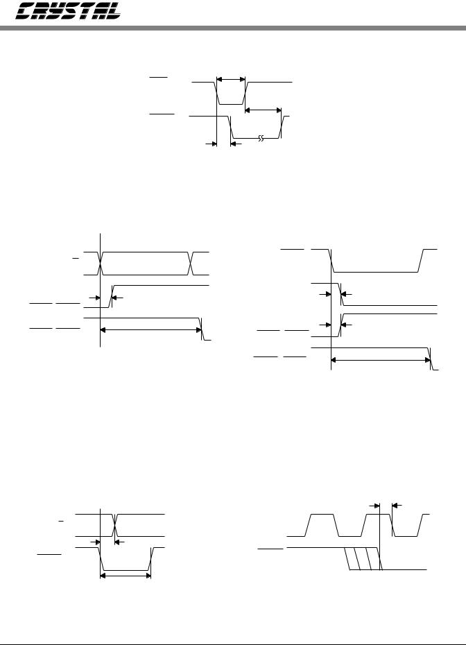
Reset and Calibration Timing
CH1/2 |
|
HOLD |
|
|
|
|
|
SSH/SDL |
TRK1,TRK2 |
tdrsh1 |
|
|
|
|
TRK1,TRK2 |
tdfsh4 |
SSH,TRK1,TRK2 |
|
|
|
|
|
TRK1,TRK2 |
|
a. FRN Mode |
|
|
|
Control Output Timing |
CH1/2
CLKIN
tdhlri
HOLD
HOLD
thold
tdfsh2
tdrsh
tdfsh1
b. PDT, RBT Mode
thcf
Channel Selection Timing |
Start Conversion Timing |
8 |
DS45F2 |

CS5101A CS5102A
SWITCHING CHARACTERISTICS (Continued)
Parameter |
|
Symbol |
Min |
Typ |
Max |
Units |
|
|
|
|
|
|
|
PDT and RBT Modes |
|
|
|
|
|
|
|
|
|
|
|
|
|
SCLK Input Pulse Period |
|
tsclk |
200 |
- |
- |
ns |
SCLK Input Pulse Width Low |
|
tsclkl |
50 |
- |
- |
ns |
SCLK Input Pulse Width High |
|
tsclkh |
50 |
- |
- |
ns |
SCLK Input Falling to SDATA Valid |
|
tdss |
- |
100 |
150 |
ns |
HOLD Falling to SDATA Valid |
PDT Mode |
tdhs |
- |
140 |
230 |
ns |
TRK1, TRK2 Falling to SDATA Valid |
(Note 30) |
tdts |
- |
65 |
125 |
ns |
FRN and SSC Modes |
|
|
|
|
|
|
|
|
|
|
|
|
|
SCLK Output Pulse Width Low |
|
tslkl |
- |
2tclk |
- |
tclk |
SCLK Output Pulse Width High |
|
tslkh |
- |
2tclk |
- |
tclk |
SDATA Valid Before Rising SCLK |
|
tss |
2tclk-100 |
- |
- |
ns |
SDATA Valid After Rising SCLK |
|
tsh |
2tclk-100 |
- |
- |
ns |
SDL Falling to 1st Rising SCLK |
|
trsclk |
- |
2tclk |
- |
ns |
Last Rising SCLK to SDL Rising |
CS5101A |
trsdl |
- |
2tclk |
2tclk+165 |
ns |
|
CS5102A |
trsdl |
- |
2tclk |
2tclk+200 |
ns |
HOLD Falling to 1st Falling SCLK |
CS5101A |
thfs |
6tclk |
- |
8tclk+165 |
ns |
|
CS5102A |
thfs |
6tclk |
- |
8tclk+200 |
ns |
CH1/2 Edge to 1st Falling SCLK |
|
tchfs |
- |
7tclk |
- |
tclk |
Note: 30. Only valid for TRK1, TRK2 falling when SCLK is low. If SCLK is high when TRK1, TRK2 falls, then SDATA is valid tdss time after the next falling SCLK.
DIGITAL CHARACTERISTICS (TA = Tmin to Tmax; VA+, VD+ = 5V ± 10%; VA-, VD- = 5V ± 10%)
Parameter |
|
Symbol |
Min |
Typ |
Max |
Units |
|
|
|
|
|
|
|
Calibration Memory Retention |
(Note 31) |
VMR |
2.0 |
- |
- |
V |
Power Supply Voltage VA+ and VD+ |
|
|
|
|
|
|
High-Level Input Voltage |
|
VIH |
2.0 |
- |
- |
V |
Low-Level Input Voltage |
|
VIL |
- |
- |
0.8 |
V |
High-Level Output Voltage |
(Note 32) |
VOH |
(VD+)-1.0 |
- |
- |
V |
Low-Level Output Voltage |
IOUT = 1.6 mA |
VOL |
- |
- |
0.4 |
V |
Input Leakage Current |
|
Iin |
- |
- |
10 |
μA |
|
|
|
|
|
|
|
Digital Output Pin Capacitance |
|
Cout |
- |
9 |
- |
pF |
Notes: 31. VAand VDcan be any value from zero to -5V for memory retention. Neither VAor VDshould be allowed to go positive. AIN1, AIN2 or VREF must not be greater than VA+ or VD+.
This parameter is guaranteed by characterization.
32. IOUT = -100 μA. This specification guarantees TTL compatibility (VOH = 2.4V @ Iout = -40 μA).
DS45F2 |
9 |
CS5101A CS5102A
|
HOLD |
thfs |
|
|
|
|
|
tchfs |
|
|
|
|
CH1/2 |
|
|
|
|
|
SSH/SDL |
|
|
|
|
|
|
trsclk |
|
|
|
tsclkl |
tsclkh |
tslkl |
tslkh |
tdss |
trsdl |
|
SCLK |
|
|
|
|
SCLK |
tsclk |
|
|
|
|
tdss |
|
tss |
tsh |
|
|
|
|
|
|
||
SDATA |
SDATA |
|
MSB |
|
LSB |
a. SCLK input (RBT and PDT mode) |
b. SCLK output (SSC and FRN modes) |
||||
|
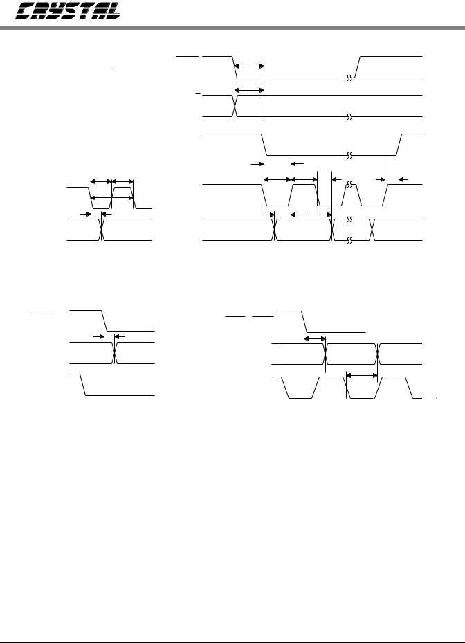
Serial Data Timing |
|
|
|
|
HOLD |
|
TRK1, TRK2 |
tdts |
|
|
tdhs |
|
|
|
||
|
|
|
|
||
SDATA |
MSB |
SDATA |
|
MSB |
MSB-1 |
SCLK |
|
SCLK |
|
tdss |
|
|
|
|
|
||
|
|
|
|
|
|
a. Pipelined Data Transmission (PDT) |
b. Register Burst Transmission (RBT) Mode |
||||
Data Transmission Timing
10 |
DS45F2 |
CS5101A CS5102A
RECOMMENDED OPERATING CONDITIONS (AGND, DGND = 0V, see Note 33)
|
Parameter |
|
Symbol |
Min |
Typ |
Max |
Units |
|
|
|
|
|
|
|
|
DC Power Supplies: |
Positive Digital |
|
VD+ |
4.5 |
5.0 |
VA+ |
V |
|
Negative Digital |
|
VD- |
-4.5 |
-5.0 |
-5.5 |
V |
|
Positive Analog |
|
VA+ |
4.5 |
5.0 |
5.5 |
V |
|
Negative Analog |
|
VA- |
-4.5 |
-5.0 |
-5.5 |
V |
Analog Reference Voltage |
|
VREF |
2.5 |
4.5 |
(VA+)-0.5 |
V |
|
Analog Input Voltage: |
|
(Note 34) |
|
|
|
|
|
|
Unipolar |
|
VAIN |
AGND |
- |
VREF |
V |
|
Bipolar |
|
VAIN |
-VREF |
- |
VREF |
V |
Notes: 33. All voltages with respect to ground.
34.The CS5101A and CS5102A can accept input voltages up to the analog supplies (VA+ and VA-). They will produce an output of all 1’s for inputs above VREF and all 0’s for inputs below AGND in unipolar mode and -VREF in bipolar mode, with binary coding (CODE = low).
ABSOLUTE MAXIMUM RATINGS* (AGND, DGND = 0V, all voltages with respect to ground)
|
Parameter |
|
Symbol |
Min |
Typ |
Max |
Units |
|
|
|
|
|
|
|
|
DC Power Supplies: |
Positive Digital |
(Note 35) |
VD+ |
-0.3 |
- |
6.0 |
V |
|
Negative Digital |
|
VD- |
0.3 |
- |
-6.0 |
V |
|
Positive Analog |
|
VA+ |
-0.3 |
- |
6.0 |
V |
|
Negative Analog |
|
VA- |
0.3 |
- |
-6.0 |
V |
Input Current, Any Pin Except Supplies |
(Note 36) |
Iin |
- |
- |
±10 |
mA |
|
|
|
|
|
|
|
|
|
Analog Input Voltage |
(AIN and VREF pins) |
|
VINA |
(VA-)-0.3 |
- |
(VA+)+0.3 |
V |
Digital Input Voltage |
|
|
VIND |
-0.3 |
- |
(VA+)+0.3 |
V |
Ambient Operating Temperature |
|
TA |
-55 |
- |
125 |
°C |
|
Storage Temperature |
|
|
Tstg |
-65 |
- |
150 |
°C |
|
|
|
|
|
|
|
|
Ambient Operating Temperature |
|
TA |
-55 |
- |
125 |
°C |
|
Storage Temperature |
|
|
Tstg |
-65 |
- |
150 |
°C |
|
|
|
|
|
|
|
|
Notes: 35. In addition, VD+ must not be greater than (VA+) +0.3V
36. Transient currents of up to 100 mA will not cause SCR latch-up.
*WARNING: Operation beyond these limits may result in permanent damage to the device.
DS45F2 |
11 |
CS5101A CS5102A
GENERAL DESCRIPTION
The CS5101A and CS5102A are 2-channel, 16bit A/D converters. The devices include an inherent sample/hold and an on-chip analog switch for 2-channel operation. Both channels can thus be sampled and converted at rates up to 50 kHz each (CS5101A) or 10 kHz each (CS5102A). Alternatively, each of the devices can be operated as a single channel ADC operating at 100 kHz (CS5101A) or 20 kHz (CS5102A).
Both the CS5101A and CS5102A can be configured to accept either unipolar or bipolar input ranges, and data is output serially in either binary or 2’s complement coding. The devices can be configured in 3 different output modes, as well as an internal, synchronous loopback mode. The CS5101A and CS5102A provide coarse charge/fine charge control, to allow accurate tracking of high-slew signals.
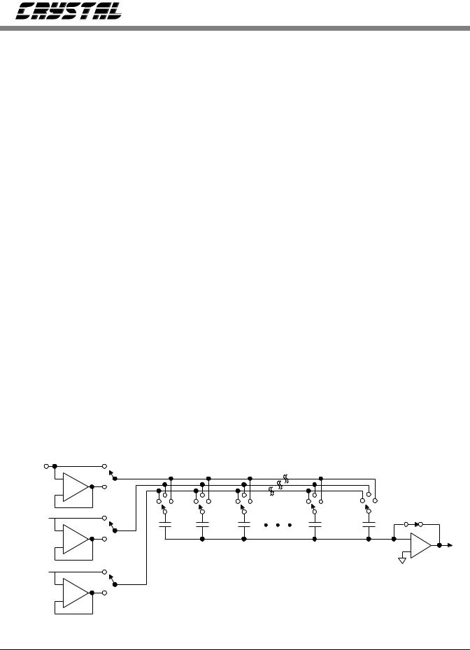
THEORY OF OPERATION
The CS5101A and CS5102A implement the successive approximation algorithm using a charge redistribution architecture. Instead of the traditional resistor network, the DAC is an array of binary-weighted capacitors. All capacitors in the
Fine
AIN
array share a common node at the comparator’s input. As shown in Figure 1, their other terminals are capable of being connected to AGND, VREF, or AIN (1 or 2). When the device is not calibrating or converting, all capacitors are tied to AIN. Switch S1 is closed and the charge on the array, tracks the input signal.
When the conversion command is issued, switch S1 opens. This traps the charge on the comparator side of the capacitor array and creates a floating node at the comparator’s input. The conversion algorithm operates on this fixed charge, and the signal at the analog input pin is ignored. In effect, the entire DAC capacitor array serves as analog memory during conversion much like a hold capacitor in a sample/hold amplifier.
The conversion consists of manipulating the free plates of the capacitor array to VREF and AGND to form a capacitive divider. Since the charge at the floating node remains fixed, the voltage at that point depends on the proportion of capacitance tied to VREF versus AGND. The successive-approximation algorithm is used to find the proportion of capacitance, which when connected to the reference will drive the voltage at the floating node to zero. That binary fraction of capacitance represents the converter’s digital output.
+
-
VREF 

+
-
AGND 

+
-
Coarse |
|
|
|
|
|
Fine |
C/2 |
C/4 |
C/32,768 |
C/32,768 |
S1 |
C |
|
|
|
|
|
|
- |
Coarse |
Bit 15 |
Bit 14 |
Bit 13 |
Bit 0 |
Dummy |
+ |
Fine |
MSB |
|
|
LSB |
|
|
|
|
|
|
|
|
|
|
|
Ctot = C + C/2 + C/4 + C/8 + ... C/32,768 |
|
|
||
Coarse |
|
|
|
|
|
|
Figure 1. Coarse Charge Input Buffers and Charge Redistribution DAC
12 |
DS45F2 |
Loading...