


 Loading...
CS4398
120 dB, 192 kHz Multi-Bit DAC with Volume Control
Features
Advanced Multi-bit Delta-Sigma Architecture
–120 dB Dynamic Range
–-107 dB THD+N
–Low Clock Jitter Sensitivity
–Differential Analog Outputs
PCM input
–102 dB of Stopband Attenuation
–Supports Sample Rates up to 192 kHz
–Accepts up to 24 bit Audio Data
–Supports All Industry Standard Audio Interface Formats
–Selectable Digital Filter Response
–Volume Control with 1/2 dB Step Size and Soft Ramp
–Flexible Channel Routing and Mixing
–Selectable De-Emphasis
Supports Stand-Alone or I²C/SPI™ Configuration
Embedded Level Translators
–1.8 V to 5 V Serial Audio Input
–1.8 V to 5 V Control Data Input
Direct Stream Digital (DSD)
–Dedicated DSD Input Pins
–On-Chip 50 kHz Filter to Meet Scarlet Book SACD Recommendations
–Matched PCM and DSD Analog Output Levels
–Non-Decimating Volume Control with 1/2 dB Step Size and Soft Ramp
–DSD Mute Detection
–Supports Phase-Modulated Inputs
–Optional Direct DSD Path to On-Chip Switched Capacitor Filter
Control Output for External Muting
–Independent Left and Right Mute Controls
–Supports Auto Detection of Mute Output Polarity
Typical Applications
–DVD Players
–SACD Players
–A/V Receivers
–Professional Audio Products
|
|
|
|
3.3 V to 5 V |
|
|
5 V |
|
|
1.8 V to 5 V |
Level Translator |
|
|
|
|
|
Switched |
|
|
|
Register/Hardware |
Interpolation |
|
Multibit |
|
Left |
|||
Hardware or I2C/SPI |
MUX |
|
Capacitor |
||||||
Filter with |
MUX |
||||||||
Control Data |
Configuration |
∆Σ Modulator |
DAC and |
Differential |
|||||
|
Volume Control |
Output |
|||||||
|
|
||||||||
|
|
|
|
|
|
|
Filter |
|
|
1.8 V to 5V |
|
|
Interpolation |
|
|
|
Switched |
|
|
|
|
|
|
Multibit |
|
Right |
|||
|
|
PCM |
MUX |
|
Capacitor |
||||
|
|
Filter with |
∆Σ Modulator |
MUX |
Differential |
||||
PCM Input |
|
Serial |
Volume Control |
DAC and |
Output |
||||
|
Translator |
Interface |
|
|
Filter |
|
|||
|
|
|
|
External |
|
||||
|
Level |
|
|
|
|
|
Left and Right |
||
|
|
DSD Processor |
|
|
Mute |
||||
|
|
|
|
Mute Controls |
|||||
|
DSD |
|
|
Control |
|||||
DSD Input |
|
-Volume control |
|
|
|
||||
|
Interface |
|
|
|
|
||||
|
-50kHz filter |
|
|
|
|
||||
|
|
|
|
|
|
||||
|
|
|
|
|
|
|
|||
|
|
|
|
|
|
|
Internal Voltage |
|
|
|
|
|
Direct DSD |
|
|
Reference |
|
||
|
|
|
|
|
|
|
|||
|
Copyright ♥ Cirrus Logic, Inc. 2005 |
JULY '05 |
http://www.cirrus.com |
(All Rights Reserved) |
DS568F1 |
CS4398
Stand-Alone Mode Features
Selectable Oversampling Modes
–32 kHz to 54 kHz Sampling Rates
–50 kHz to 108 kHz Sampling Rates
–100 kHz to 216 kHz Sampling Rates
Selectable Serial Audio Interface Formats
–Left-Justified, up to 24 bit
–I²S, up to 24 bit
–Right-Justified 16 bit
–Right-Justified 24 bit
Auto Mute Output Polarity Detect
Auto Mute on Static PCM Samples
44.1 kHz 50/15 s De-Emphasis Available
Soft Volume Ramp-up after Reset is Released
Control Port Mode Features
Selectable Oversampling Modes
–32 kHz to 54 kHz Sampling Rates
–50 kHz to 108 kHz Sampling Rates
–100 kHz to 216 kHz Sampling Rates
Selectable Serial Audio Interface Formats
–Left-Justified, up to 24 bit
–I²S, up to 24 bit
–Right-Justified 16 bit
–Right-Justified 18 bit
–Right-Justified 20 bit
–Right-Justified 24 bit
ORDERING INFORMATION
Direct Stream Digital Mode
Selectable Auto or Manual Mute Polarity
Selectable Interpolation Filters
Selectable 32, 44.1, and 48 kHz De-Emphasis
Configurable ATAPI Mixing Functions
Configurable Volume and Muting Controls
Description
The CS4398 is a complete stereo 24 bit/192 kHz digital- to-analog system. This D/A system includes digital deemphasis, half dB step size volume control, ATAPI channel mixing, selectable fast and slow digital interpolation filters followed by an oversampled multi-bit deltasigma modulator that includes mismatch shaping technology that eliminates distortion due to capacitor mismatch. Following this stage is a multi-element switched capacitor stage and low pass filter with differential analog outputs.
The CS4398 also has an proprietary DSD processor that allows for volume control and 50 kHz on-chip filtering without an intermediate decimation stage. It also offers an optional path for direct DSD conversion by directly using the multi-element switched capacitor array.
The CS4398 accepts PCM data at sample rates from 32 kHz to 216 kHz, DSD audio data, has selectable digital filters, consumes little power, and delivers excellent sound quality.
Product |
Description |
Package |
Pb-Free |
Grade |
Temp Range |
Container |
Order # |
|
|
120 dB, 192 kHz Multi- |
28-pin |
|
|
|
Rail |
CS4398-CZZ |
|
CS4398 |
Bit DAC with Volume |
YES |
Commercial |
-10° to +70° C |
|
|
||
TSSOP |
Tape & Reel |
CS4398-CZZR |
||||||
|
Control |
|
|
|
||||
|
|
|
|
|
|
|
||
CDB4398 |
CS4398 Evaluation |
Board |
- |
- |
- |
- |
CDB4398 |
|
|
|
|
|
|
|
|
|
|
2 |
|
|
|
|
|
|
DS568F1 |

|
|
CS4398 |
TABLE OF CONTENTS |
|
|
1. PINOUT DRAWING ................................................................................................................. |
6 |
|
2. CHARACTERISTICS AND SPECIFICATIONS ........................................................................ |
8 |
|
SPECIFIED OPERATING CONDITIONS................................................................................. |
8 |
|
ABSOLUTE MAXIMUM RATINGS ........................................................................................... |
8 |
|
ANALOG CHARACTERISTICS................................................................................................ |
9 |
|
COMBINED INTERPOLATION & ON-CHIP ANALOG FILTER RESPONSE ........................ |
10 |
|
COMBINED INTERPOLATION & ON-CHIP ANALOG FILTER RESPONSE ........................ |
11 |
|
DSD COMBINED DIGITAL AND ON-CHIP ANALOG FILTER RESPONSE.......................... |
11 |
|
SWITCHING CHARACTERISTICS ........................................................................................ |
12 |
|
SWITCHING CHARACTERISTICS - DSD ............................................................................. |
14 |
|
SWITCHING CHARACTERISTICS - CONTROL PORT - I²C FORMAT ................................ |
15 |
|
SWITCHING CHARACTERISTICS - CONTROL PORT - SPI™ FORMAT............................ |
16 |
|
DC ELECTRICAL CHARACTERISTICS ............................................................................... |
17 |
|
DIGITAL INTERFACE SPECIFICATIONS ............................................................................. |
18 |
|
3. TYPICAL CONNECTION DIAGRAM .................................................................................. |
19 |
|
4. APPLICATIONS ..................................................................................................................... |
20 |
|
4.1 |
Grounding and Power Supply Decoupling ....................................................................... |
20 |
4.2 |
Analog Output and Filtering ............................................................................................. |
20 |
4.3 The MUTEC Outputs ....................................................................................................... |
20 |
|
4.4 |
Oversampling Modes ....................................................................................................... |
21 |
4.5 |
Master and Serial Clock Ratios ....................................................................................... |
21 |
4.6 |
Stand-Alone Mode Settings ............................................................................................. |
22 |
4.7 |
Control Port Mode ........................................................................................................... |
23 |
5. CONTROL PORT INTERFACE ............................................................................................. |
25 |
|
5.1 |
Memory Address Pointer (MAP) ...................................................................................... |
25 |
5.2 |
Enabling the Control Port ................................................................................................ |
25 |
5.3 |
Format Selection ............................................................................................................. |
25 |
5.4 |
I²C Format ....................................................................................................................... |
25 |
5.5 |
SPI Format ...................................................................................................................... |
26 |
7.1 |
Chip ID - Register 01h ..................................................................................................... |
29 |
7.2 |
Mode Control 1 - Register 02h ........................................................................................ |
29 |
7.3 |
Volume Mixing and Inversion Control - Register 03h ...................................................... |
30 |
7.4 |
Mute Control - Register 04h ............................................................................................ |
33 |
7.5 |
Channel A Volume Control - Register 05h ....................................................................... |
34 |
7.6 |
Channel B Volume Control - Register 06h ....................................................................... |
34 |
7.7 |
Ramp and Filter Control - Register 07h ........................................................................... |
35 |
7.8 |
Misc. Control - Register 08h ............................................................................................ |
37 |
7.9 |
Misc. Control - Register 09h ............................................................................................ |
38 |
8. PARAMETER DEFINITIONS .................................................................................................. |
39 |
|
9. REFERENCES ........................................................................................................................ |
39 |
|
10. PACKAGE DIMENSIONS .................................................................................................... |
40 |
|
10.1 28-TSSOP ..................................................................................................................... |
40 |
|
THERMAL CHARACTERISTICS AND SPECIFICATIONS ................................................... |
40 |
|
11. APPENDIX ....................................................................................................................... |
41 |
|
DS568F1 |
3 |

|
CS4398 |
LIST OF FIGURES |
|
Figure 1. Pinout Drawing................................................................................................................. |
6 |
Figure 2. Serial Mode Input Timing ............................................................................................... |
12 |
Figure 3. Format 0 - Left-Justified up to 24-bit Data ..................................................................... |
13 |
Figure 4. Format 1 - I²S up to 24-bit Data ..................................................................................... |
13 |
Figure 5. Format 2, Right-Justified 16-Bit Data. |
|
Format 3, Right-Justified 24-Bit Data. |
|
Format 4, Right-Justified 20-Bit Data. (Available in Control Port Mode only) |
|
Format 5, Right-Justified 18-Bit Data. (Available in Control Port Mode only) ................ |
13 |
Figure 6. Direct Stream Digital - Serial Audio Input Timing........................................................... |
14 |
Figure 7. Direct Stream Digital - Serial Audio Input Timing for Phase Modulation Mode.............. |
14 |
Figure 8. Control Port Timing - I²C Format.................................................................................... |
15 |
Figure 9. Control Port Timing - SPI Format (Read/Write) ............................................................. |
16 |
Figure 10. Typical Connection Diagram........................................................................................ |
19 |
Figure 11. Recommended Output Filter........................................................................................ |
20 |
Figure 12. Recommended Mute Circuitry ..................................................................................... |
21 |
Figure 13. DSD Phase Modulation Mode Diagram ....................................................................... |
24 |
Figure 14. Control Port Timing, I²C Format................................................................................... |
26 |
Figure 15. Control Port Timing, SPI Format (Write) ...................................................................... |
27 |
Figure 16. Control Port Timing, SPI Format (Read)...................................................................... |
27 |
Figure 17. De-Emphasis Curve..................................................................................................... |
30 |
Figure 18. ATAPI Block Diagram .................................................................................................. |
31 |
Figure 19. 28L TSSOP (4.4 mm Body) Package Drawing ............................................................ |
40 |
Figure 20. Single-Speed (fast) Stopband Rejection...................................................................... |
41 |
Figure 21. Single-Speed (fast) Transition Band ............................................................................ |
41 |
Figure 22. Single-Speed (fast) Transition Band (detail) ................................................................ |
41 |
Figure 23. Single-Speed (fast) Passband Ripple .......................................................................... |
41 |
Figure 24. Single-Speed (slow) Stopband Rejection .................................................................... |
41 |
Figure 25. Single-Speed (slow) Transition Band........................................................................... |
41 |
Figure 26. Single-Speed (slow) Transition Band (detail)............................................................... |
42 |
Figure 27. Single-Speed (slow) Passband Ripple......................................................................... |
42 |
Figure 28. Double-Speed (fast) Stopband Rejection .................................................................... |
42 |
Figure 29. Double-Speed (fast) Transition Band........................................................................... |
42 |
Figure 30. Double-Speed (fast) Transition Band (detail)............................................................... |
42 |
Figure 31. Double-Speed (fast) Passband Ripple......................................................................... |
42 |
Figure 32. Double-Speed (slow) Stopband Rejection ................................................................... |
43 |
Figure 33. Double-Speed (slow) Transition Band ......................................................................... |
43 |
Figure 34. Double-Speed (slow) Transition Band (detail) ............................................................. |
43 |
Figure 35. Double-Speed (slow) Passband Ripple ....................................................................... |
43 |
Figure 36. Quad-Speed (fast) Stopband Rejection ....................................................................... |
43 |
Figure 37. Quad-Speed (fast) Transition Band ............................................................................. |
43 |
Figure 38. Quad-Speed (fast) Transition Band (detail) ................................................................. |
44 |
Figure 39. Quad-Speed (fast) Passband Ripple ........................................................................... |
44 |
Figure 40. Quad-Speed (slow) Stopband Rejection...................................................................... |
44 |
Figure 41. Quad-Speed (slow) Transition Band............................................................................ |
44 |
Figure 42. Quad-Speed (slow) Transition Band (detail)................................................................ |
44 |
Figure 43. Quad-Speed (slow) Passband Ripple.......................................................................... |
44 |
4 |
DS568F1 |

|
|
CS4398 |
LIST OF TABLES |
|
|
Table 1. Clock Ratios .................................................................................................................... |
21 |
|
Table 2. Common Clock Frequencies........................................................................................... |
22 |
|
Table 3. Digital Interface Format, Stand-Alone Mode Options...................................................... |
22 |
|
Table 4. Mode Selection, Stand-Alone Mode Options .................................................................. |
22 |
|
Table 5. |
Digital Interface Formats - PCM Mode............................................................................ |
29 |
Table 6. |
Digital Interface Formats - DSD Mode ............................................................................ |
30 |
Table 7. |
Example Digital Volume Settings .................................................................................... |
34 |
Table 8. |
Revision Table ................................................................................................................ |
45 |
DS568F1 |
5 |

CS4398
1. PINOUT DRAWING
DSD_B |
|
|
|
|
|
1 |
28 |
|
|
DSD_A |
||||||||||||||
|
|
|
|
|
|
|
||||||||||||||||||
DSD_SCLK |
|
|
|
|
|
2 |
27 |
|
|
VLS |
||||||||||||||
|
|
|
|
|
|
|
|
|||||||||||||||||
SDIN |
|
|
|
|
|
3 |
26 |
|
|
VQ |
||||||||||||||
|
|
|
|
|
|
|
|
|
||||||||||||||||
SCLK |
|
|
|
|
|
4 |
25 |
|
|
AMUTEC |
||||||||||||||
|
|
|
|
|
|
|
|
|
|
|||||||||||||||
LRCK |
|
|
|
|
|
5 |
24 |
|
|
AOUTA- |
||||||||||||||
|
|
|
|
|
|
|
|
|
|
|
||||||||||||||
MCLK |
|
|
|
|
|
6 |
23 |
|
|
AOUTA+ |
||||||||||||||
|
|
|
|
|
|
|
|
|
|
|
|
|||||||||||||
|
|
VD |
|
|
|
|
|
7 |
22 |
|
|
VA |
||||||||||||
|
|
|
|
|
|
|
|
|
|
|
|
|
|
|
||||||||||
DGND |
|
|
|
|
|
8 |
21 |
|
|
AGND |
||||||||||||||
|
|
|
|
|
|
|
|
|
|
|
|
|
|
|||||||||||
M3 (AD1/CDIN) |
|
|
|
|
|
9 |
20 |
|
|
AOUTB+ |
||||||||||||||
|
|
|
|
|
|
|
|
|
|
|
|
|
|
|
||||||||||
M2 (SCL/CCLK) |
|
|
|
|
10 |
19 |
|
|
AOUTB- |
|||||||||||||||
|
|
|
|
|
|
|||||||||||||||||||
M1 (SDA/CDOUT) |
|
|
|
|
|
11 |
18 |
|
|
BMUTEC |
||||||||||||||
|
|
|
|
|
|
|
|
|
|
|
|
|
|
|
|
|||||||||
|
|
|
|
|
|
|
|
|
|
|
|
|
|
|
|
|
|
|
|
|
|
|
|
|
M0 (AD0/CS) |
|
|
|
|
|
|
|
|
|
|
|
|
|
|
|
|
|
12 |
17 |
|
|
VREF |
||
|
|
|
|
|
|
|
|
|
|
|
|
|
|
|
|
|
|
|
||||||
|
|
|
|
|
|
|
|
|
|
|
|
|
|
|
|
|
|
|
||||||
|
|
|
|
|
|
|
|
|
|
|
|
|
|
|
|
|
|
|
|
|
REF_GND |
|||
|
RST |
|
|
|
|
|
|
|
|
|
|
|
|
|
|
|
|
13 |
16 |
|
|
|||
|
|
|
|
|
|
|
|
|
|
|
|
|
|
|
|
|
|
|
||||||
|
VLC |
|
|
|
|
|
14 |
15 |
|
|
FILT+ |
|||||||||||||
|
|
|
|
|
|
|
|
|||||||||||||||||
|
|
|
|
|
|
|
|
|||||||||||||||||
|
|
|
|
|
|
|
|
|
|
|
|
|
|
|
|
|
|
|
|
|
|
|
|
|
Figure 1. Pinout Drawing
6 |
DS568F1 |

|
|
|
|
|
|
|
|
CS4398 |
|
|
|
|
|
|
|
|
|
|
|
|
|
|
|
|
|
|
|||
|
Pin Name |
Pin # |
|
|
|
Pin Description |
|||
|
|
|
|
|
|
|
|
||
|
DSD_A |
28 |
Direct Stream Digital Input (Input) - Input for Direct Stream Digital serial audio data. |
||||||
|
DSD_B |
1 |
|||||||
|
|
|
|
|
|
||||
|
|
|
|
||||||
|
DSD_SCLK |
2 |
DSD Serial Clock (Input) - Serial clock for the Direct Stream Digital audio interface. |
||||||
|
SDIN |
3 |
Serial Audio Data Input (Input) - Input for two’s complement serial audio data. |
||||||
|
SCLK |
4 |
Serial Clock (Input) - Serial clock for the serial audio interface. |
||||||
|
LRCK |
5 |
Left Right Clock (Input) - Determines which channel, Left or Right, is currently active on |
||||||
|
the serial audio data line. |
||||||||
|
|
|
|
|
|||||
|
MCLK |
6 |
Master Clock (Input) - Clock source for the delta-sigma modulator and digital filters. |
||||||
|
VD |
7 |
Digital Power (Input) - Positive power for the digital section. |
||||||
|
DGND |
8 |
Digital Ground (Input) - Ground reference for the digital section. |
||||||
|
RST |
13 |
Reset |
(Input) - The device enters system reset when enabled. |
|||||
|
VLC |
14 |
Control Port Power (Input) - Positive power for Control Port I/O. |
||||||
|
FILT+ |
15 |
Positive Voltage Reference (Output) - Positive reference voltage for the internal sam- |
||||||
|
pling circuits. |
||||||||
|
|
|
|
|
|||||
|
REF_GND |
16 |
Reference Ground (Input) - Ground reference for the internal sampling circuits. |
||||||
|
VREF |
17 |
Voltage Reference (Input) - Positive voltage reference for the internal sampling circuits. |
||||||
|
BMUTEC |
18 |
Mute Control (Output) - The Mute Control pin is active during power-up initialization, mut- |
||||||
|
ing, power-down or if the master clock to left/right clock frequency ratio is incorrect. During |
||||||||
|
AMUTEC |
25 |
|||||||
|
reset, these outputs are set to a high impedance. |
||||||||
|
|
|
|
|
|||||
|
|
|
|
||||||
|
AOUTB+ |
20 |
Differential Right Channel Analog Output (Output) - The full-scale differential analog |
||||||
|
AOUTB- |
19 |
output level is specified in the Analog Characteristics specification table. |
||||||
|
AGND |
21 |
Analog Ground (Input) - Ground reference for the analog section. |
||||||
|
VA |
22 |
Analog Power (Input) - Positive power for the analog section. |
||||||
|
AOUTA+ |
23 |
Differential Left Channel Analog Output (Output) - The full-scale differential analog out- |
||||||
|
AOUTA- |
24 |
put level is specified in the Analog Characteristics specification table. |
||||||
|
VQ |
26 |
Quiescent Voltage (Output) - Filter connection for internal quiescent voltage. |
||||||
|
VLS |
27 |
Serial Audio Interface Power (Input) - Positive power for serial audio interface I/O. |
||||||
|
Stand-Alone Mode Definitions |
||||||||
|
|
|
|
|
|
|
|
||
|
M3 |
9 |
|
|
|
|
|
||
|
M2 |
10 |
Mode Selection (Input) - Determines the operational mode of the device. |
||||||
|
M1 |
11 |
|||||||
|
|
|
|
|
|
||||
|
M0 |
12 |
|
|
|
|
|
||
|
|
||||||||
|
Control Port Mode Definitions |
||||||||
|
|
|
|
|
|
||||
|
AD1/CDIN |
9 |
Address Bit 1 (I²C) / Control Data Input (SPI) (Input) - AD1 is a chip address pin in I²C |
||||||
|
mode; CDIN is the input data line for the Control Port interface in SPI mode. |
||||||||
|
|
|
|
|
|||||
|
SCL/CCLK |
10 |
Serial Control Port Clock (Input) - Serial clock for the serial Control Port. |
||||||
|
SDA/CDOUT |
11 |
Serial Control Data (I²C) / Control Data Output (SPI) (Input/Output) - SDA is a data I/O |
||||||
|
line in I²C mode. CDOUT is the output data line for the Control Port interface in SPI mode. |
||||||||
|
|
|
|
|
|||||
|
|
|
|
|
Address Bit 0 (I²C) / Control Port Chip Select (SPI) (Input) - AD0 is a chip address pin |
||||
|
AD0/CS |
12 |
|||||||
|
|
|
|
|
|
||||
|
in I²C mode; CS is the chip select signal for SPI format. |
||||||||
|
|
|
|
|
|||||
DS568F1 |
7 |

CS4398
2. CHARACTERISTICS AND SPECIFICATIONS
(Min/Max performance characteristics and specifications are guaranteed over the Specified Operating Conditions. Typical performance characteristics are derived from measurements taken at TA = 25 °C, VA = 5.0 V, VD = 3.3 V.)
SPECIFIED OPERATING CONDITIONS
(AGND = 0 V; all voltages with respect to ground.)
Parameters |
Symbol |
Min |
Typ |
Max |
Units |
|
DC Power Supply |
Analog power |
VA |
4.75 |
5.0 |
5.25 |
V |
|
Voltage reference |
VREF |
4.75 |
5.0 |
5.25 |
V |
|
Digital power |
VD |
3.1 |
3.3 |
5.25 |
V |
|
Serial audio interface power |
VLS |
1.7 |
3.3 |
5.25 |
V |
|
Control port interface power |
VLC |
1.7 |
3.3 |
5.25 |
V |
Specified Temperature Range |
-CZ & -CZZ |
TA |
-10 |
- |
70 |
°C |
ABSOLUTE MAXIMUM RATINGS
(AGND = 0 V; all voltages with respect to ground.)
|
Parameters |
Symbol |
Min |
Max |
Units |
DC Power Supply |
Analog power |
VA |
-0.3 |
6.0 |
V |
|
Voltage reference |
VREF |
-0.3 |
6.0 |
V |
|
Digital power |
VD |
-0.3 |
6.0 |
V |
|
Serial audio interface power |
VLS |
-0.3 |
6.0 |
V |
|
Control port interface power |
VLC |
-0.3 |
6.0 |
V |
Input Current |
any pin except supplies |
Iin |
- |
±10 |
mA |
Digital Input Voltage |
Serial audio interface |
VIN-LS |
-0.3 |
VLS+ 0.4 |
V |
|
Control port interface |
VIN-LC |
-0.3 |
VLC+ 0.4 |
V |
Ambient Operating Temperature (power applied) |
TA |
-55 |
125 |
°C |
|
Storage Temperature |
|
Tstg |
-65 |
150 |
°C |
WARNING: Operation at or beyond these limits may result in permanent damage to the device. Normal operation is not guaranteed at these extremes.
8 |
DS568F1 |

CS4398
ANALOG CHARACTERISTICS
(Test conditions (unless otherwise specified): Input test signal is a 997 Hz sine wave at 0 dBFS; measurement bandwidth is 10 Hz to 20 kHz; test load RL = 1 kΩ, CL = 10 pF.)
Parameter |
|
|
Symbol |
Min |
Typ |
Max |
Unit |
|
|
|
|
|
|
||
Dynamic Performance - All PCM modes and DSD Processor mode |
|
|
|
||||
Dynamic Range (Note 1) |
24-bit |
A-Weighted |
|
114 |
120 |
- |
dB |
|
|
unweighted |
|
111 |
117 |
- |
dB |
|
16-bit A-Weighted |
|
- |
97 |
- |
dB |
|
|
(Note 2) unweighted |
|
- |
94 |
- |
dB |
|
|
|
|
|
|
|
|
|
Total Harmonic Distortion + Noise |
|
(Note 1) |
THD+N |
- |
-107 |
-100 |
dB |
|
24-bit |
0 dB |
|
||||
|
|
-20 dB |
|
- |
-97 |
- |
dB |
|
|
-60 dB |
|
- |
-57 |
- |
dB |
|
16-bit |
0 dB |
|
- |
-94 |
- |
dB |
|
(Note 2) |
-20 dB |
|
- |
-74 |
- |
dB |
|
|
-60 dB |
|
- |
-34 |
- |
dB |
|
|
|
|
|
|
|
|
Idle Channel Noise / Signal-to-noise ratio |
|
|
- |
120 |
- |
dB |
|
|
|
|
|
|
|
|
|
Dynamic Performance - Direct DSD |
|
|
|
|
|
|
|
Dynamic Range (Note 3) |
|
A-Weighted |
|
111 |
117 |
- |
dB |
|
|
unweighted |
|
108 |
114 |
- |
dB |
|
|
|
|
|
|
|
|
Total Harmonic Distortion + Noise |
|
(Note 3) |
THD+N |
- |
-104 |
-98 |
dB |
|
|
0 dB |
|
||||
|
|
-20 dB |
|
- |
-94 |
- |
dB |
|
|
-60 dB |
|
- |
-54 |
- |
dB |
|
|
|
|
|
|
|
|
Dynamic Performance for All Modes |
|
|
|
|
|
|
|
Interchannel Isolation |
|
(1 kHz) |
|
- |
110 |
- |
dB |
|
|
|
|
|
|
|
|
DC Accuracy |
|
|
|
|
|
|
|
|
|
|
|
|
|
|
|
Interchannel Gain Mismatch |
|
|
ICGM |
- |
0.1 |
- |
dB |
|
|
|
|
|
|
|
|
Gain Drift |
|
|
|
- |
100 |
- |
ppm/°C |
|
|
|
|
|
|
||
Analog Output Characteristics and Specifications |
|
|
|
|
|
||
|
|
|
|
|
|
|
|
Full Scale Differential |
PCM, DSD processor |
|
132%•VA |
134%•VA |
136%•VA |
Vpp |
|
Output Voltage |
Direct DSD mode |
|
94%•VA |
96%•VA |
98%•VA |
Vpp |
|
Output Impedance |
|
|
ZOUT |
- |
118 |
- |
Ω |
Minimum AC-Load Resistance |
|
|
RL |
- |
1 |
- |
kΩ |
Maximum Load Capacitance |
|
|
CL |
- |
100 |
- |
pF |
Notes:
1.One-half LSB of triangular PDF dither is added to data.
2.Performance limited by 16-bit quantization noise.
3.DSD performance may be limited by the source recording. 0 dB-SACD = 50% modulation index.
DS568F1 |
9 |

CS4398
COMBINED INTERPOLATION & ON-CHIP ANALOG FILTER RESPONSE
The filter characteristics have been normalized to the sample rate (Fs) and can be referenced to the desired sample rate by multiplying the given characteristic by Fs.)
(See note 9.)
|
|
|
Fast Roll-Off |
|
|
Parameter |
|
Min |
Typ |
Max |
Unit |
Combined Digital and On-Chip Analog Filter Response - Single |
-Speed Mode - 48 kHz (Note 5) |
|
|||
Passband (Note 6) |
to -0.01 dB corner |
0 |
- |
.454 |
Fs |
|
to -3 dB corner |
0 |
- |
.499 |
Fs |
Frequency Response 10 Hz to 20 kHz |
|
-0.01 |
- |
+0.01 |
dB |
StopBand |
|
0.547 |
- |
- |
Fs |
StopBand Attenuation |
(Note 7) |
102 |
- |
- |
dB |
Group Delay |
|
- |
9.4/Fs |
- |
s |
De-emphasis Error (Note 8) |
Fs = 32 kHz |
- |
- |
±0.23 |
dB |
(Relative to 1 kHz) |
Fs = 44.1 kHz |
- |
- |
±0.14 |
dB |
|
Fs = 48 kHz |
- |
- |
±0.09 |
dB |
Combined Digital and On-Chip Analog Filter Response - Double-Speed Mode - 96 kHz (Note 5) |
|
||||
Passband (Note 6) |
to -0.01 dB corner |
0 |
- |
.430 |
Fs |
|
to -3 dB corner |
0 |
- |
.499 |
Fs |
Frequency Response 10 Hz to 20 kHz |
|
-0.01 |
- |
0.01 |
dB |
StopBand |
|
.583 |
- |
- |
Fs |
StopBand Attenuation |
(Note 7) |
80 |
- |
- |
dB |
Group Delay |
|
- |
4.6/Fs |
- |
s |
Combined Digital and On-Chip Analog Filter Response - Quad |
-Speed Mode - 192 kHz (Note 5) |
|
|||
Passband (Note 6) |
to -0.01 dB corner |
0 |
- |
.105 |
Fs |
|
to -3 dB corner |
0 |
- |
.490 |
Fs |
Frequency Response 10 Hz to 20 kHz |
|
-0.01 |
- |
0.01 |
dB |
StopBand |
|
.635 |
- |
- |
Fs |
StopBand Attenuation |
(Note 7) |
90 |
- |
- |
dB |
Group Delay |
|
- |
4.7/Fs |
- |
s |
4.Slow Roll-off interpolation filter is only available in Control Port mode.
5.Filter response is guaranteed by design.
6.Response is clock-dependent and will scale with Fs.
7.For Single-Speed Mode, the Measurement Bandwidth is from stopband to 3 Fs. For Double-Speed Mode, the Measurement Bandwidth is from stopband to 3 Fs. For Quad-Speed Mode, the Measurement Bandwidth is from stopband to 1.34 Fs.
8.De-emphasis is available only in Single-Speed Mode; Only 44.1 kHz De-emphasis is available in StandAlone mode.
9.Amplitude vs. Frequency plots of this data are available in the “Appendix” on page 41.
10 |
DS568F1 |
CS4398
COMBINED INTERPOLATION & ON-CHIP ANALOG FILTER RESPONSE
(Continued)
|
|
Slow Roll-Off (Note 4) |
|
||
Parameter |
|
Min |
Typ |
Max |
Unit |
Single-Speed Mode - 48 kHz (Note 5) |
|
|
|
|
|
Passband (Note 6) |
to -0.01 dB corner |
0 |
- |
0.417 |
Fs |
|
to -3 dB corner |
0 |
- |
0.499 |
Fs |
Frequency Response 10 Hz to 20 kHz |
|
-0.01 |
- |
+0.01 |
dB |
StopBand |
|
.583 |
- |
- |
Fs |
StopBand Attenuation |
(Note 7) |
64 |
- |
- |
dB |
Group Delay |
|
- |
6.65/Fs |
- |
s |
De-emphasis Error (Note 8) |
Fs = 32 kHz |
- |
- |
±0.23 |
dB |
(Relative to 1 kHz) |
Fs = 44.1 kHz |
- |
- |
±0.14 |
dB |
|
Fs = 48 kHz |
- |
- |
±0.09 |
dB |
Double-Speed Mode - 96 kHz (Note 5) |
|
|
|
|
|
Passband (Note 6) |
to -0.01 dB corner |
0 |
- |
.296 |
Fs |
|
to -3 dB corner |
0 |
- |
.499 |
Fs |
Frequency Response 10 Hz to 20 kHz |
|
-0.01 |
- |
0.01 |
dB |
StopBand |
|
.792 |
- |
- |
Fs |
StopBand Attenuation |
(Note 7) |
70 |
- |
- |
dB |
Group Delay |
|
- |
3.9/Fs |
- |
s |
Quad-Speed Mode - 192 kHz (Note 5) |
|
|
|
|
|
Passband (Note 6) |
to -0.01 dB corner |
0 |
- |
.104 |
Fs |
|
to -3 dB corner |
0 |
- |
.481 |
Fs |
Frequency Response 10 Hz to 20 kHz |
|
-0.01 |
- |
0.01 |
dB |
StopBand |
|
.868 |
- |
- |
Fs |
StopBand Attenuation |
(Note 7) |
75 |
- |
- |
dB |
Group Delay |
|
- |
4.2/Fs |
- |
s |
DSD COMBINED DIGITAL AND ON-CHIP ANALOG FILTER RESPONSE
Parameter |
|
Min |
Typ |
Max |
Unit |
DSD Processor Mode (Note 5) |
|
|
|
|
|
Passband (Note 6) |
to -3 dB corner |
0 |
- |
50 |
kHz |
Frequency Response 10 Hz to 20 kHz |
|
-0.05 |
- |
0.05 |
dB |
Roll-off |
|
27 |
- |
- |
dB/Oct |
Direct DSD Mode (Note 5) |
|
|
|
|
|
Passband (Note 6) |
to -0.1 dB corner |
0 |
- |
26.9 |
kHz |
|
to -3 dB corner |
0 |
- |
176.4 |
kHz |
Frequency Response 10 Hz to 20 kHz |
|
-0.1 |
- |
0 |
dB |
DS568F1 |
11 |
CS4398
SWITCHING CHARACTERISTICS
(Inputs: Logic 0 = GND, Logic 1 = VLS, CL = 20 pF)
Parameters |
|
Symbol |
|
|
Min |
Typ |
Max |
Units |
|||
Input Sample Rate |
Single-Speed Mode |
Fs |
|
30 |
|
- |
54 |
kHz |
|||
|
Double-Speed Mode |
Fs |
|
50 |
|
- |
108 |
kHz |
|||
|
Quad-Speed Mode |
Fs |
|
100 |
- |
216 |
kHz |
||||
MCLK Frequency |
|
|
See Tables |
1 & 2 (page 21) for compatible frequencies |
|||||||
MCLK Duty Cycle |
|
|
|
|
|
40% |
- |
60% |
|
||
LRCK Duty Cycle |
|
|
|
|
|
45% |
50 |
55% |
|
||
SCLK Pulse Width Low |
|
|
tsclkl |
|
20 |
|
- |
- |
ns |
||
SCLK Pulse Width High |
|
|
tsclkh |
|
20 |
|
- |
- |
ns |
||
SCLK Period |
Single-Speed Mode |
|
|
|
1 |
|
|
|
|
||
|
|
|
tsclkw |
|
-------------------- |
- |
- |
ns |
|||
|
|
|
|
(128)Fs |
|||||||
|
Double-Speed Mode |
|
|
|
|
|
|
|
|
|
|
|
tsclkw |
|
1 |
|
- |
- |
ns |
||||
|
|
|
|
----------------- |
|||||||
|
|
|
|
(64)Fs |
|||||||
|
Quad-Speed Mode |
|
|
|
|
|
|
|
|
|
|
|
t |
|
2 |
|
- |
- |
ns |
||||
|
|
|
|
---------------- |
|||||||
|
|
|
sclkw |
|
MCLK |
|
|
|
|||
|
|
|
|
|
|
|
|
|
|
|
|
SCLK rising to LRCK edge delay |
|
tslrd |
|
20 |
|
- |
- |
ns |
|||
SCLK rising to LRCK edge setup time |
|
tslrs |
|
20 |
|
- |
- |
ns |
|||
SDATA valid to SCLK rising setup time |
|
tsdlrs |
|
22 |
|
- |
- |
ns |
|||
SCLK rising to SDATA hold time |
|
tsdh |
|
20 |
|
- |
- |
ns |
|||
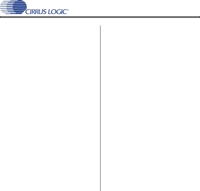
|
LR C K |
|
|
|
|
|
|
|
|
|
|
|
t slrd |
|
|
t slrs |
|
|
t sclkh |
|
|
|
|
|
|
|
|
|
t sclkl |
|
|
|
|
||
|
|
|
|
|
|
|
|
|
|||
|
S C LK |
|
|
|
|
|
|
|
|
|
|
|
t |
sdlrs |
|
|
|
|
t sdh |
|
|
|
|
|
|
|
|
|
|
|
|
||||
|
|
|
|
|
|
|
|||||
|
|
|
|
|
|
|
|
|
|
|
|
|
S D ATA |
|
|
|
|
|
|
|
|
|
|
|
Figure 2. Serial Mode Input Timing |
|
|
|
|||||||
12 |
DS568F1 |

CS4398
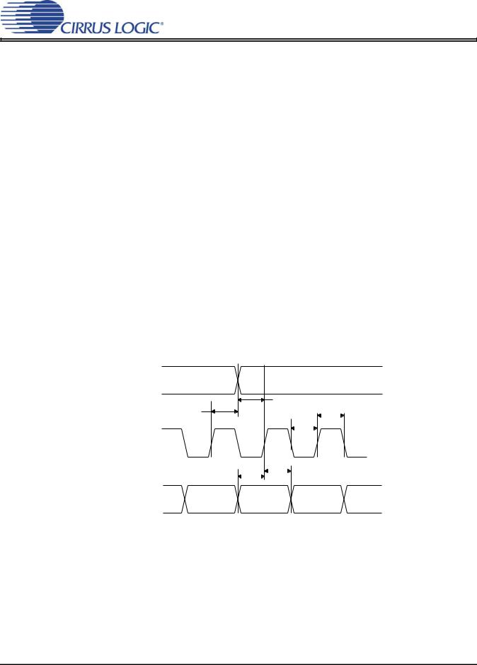
LR C K |
|
Left C hannel |
|
R ight C hannel |
|
|
|
|
|
S C L K |
|
|
|
|
S D A TA |
MSB -1 -2 -3 -4 -5 |
+5 +4 +3 +2 +1 LSB |
MSB -1 -2 -3 -4 |
+5 +4 +3 +2 +1 LSB |
Figure 3. Format 0 - Left-Justified up to 24-bit Data
LR C K |
|
Left C hannel |
|
R ig ht C han nel |
|
|
|
|
|
S C L K |
|
|
|
|
S D A T A |
MSB -1 -2 -3 -4 -5 |
+5 +4 +3 +2 +1 LSB |
MSB -1 -2 -3 -4 |
+5 +4 +3 +2 +1 LSB |
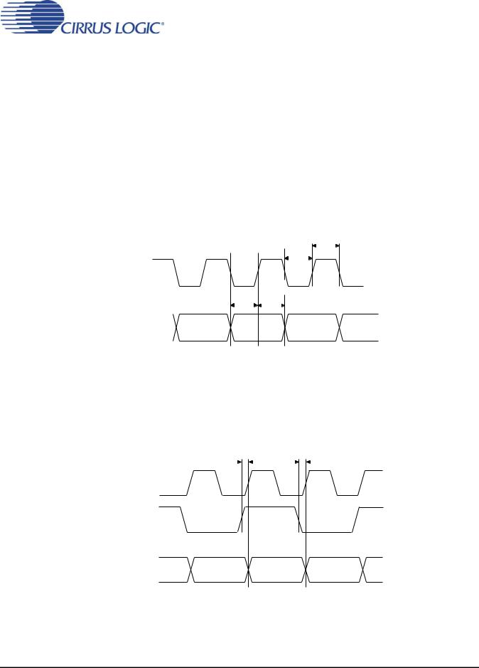
LR C K
SC LK
SD ATA LSB
Figure 4. Format 1 - I²S up to 24-bit Data
R ig h t C h a n n e l
L e ft C h a n ne l
MSB |
-1 |
-2 |
-3 |
-4 |
-5 |
-6 |
|
|
+6 |
+5 |
+4 |
+3 |
+2 |
+1 |
LSB |
MSB -1 -2 -3 -4 -5 -6 |
+6 +5 +4 +3 +2 +1 LSB |
|
|
|
|
|
|
|
|
|
|
|
|
|
|
|
|
|
|
|
|
3 2 c lo cks
Figure 5. Format 2, Right-Justified 16-Bit Data. Format 3, Right-Justified 24-Bit Data.
Format 4, Right-Justified 20-Bit Data. (Available in Control Port Mode only) Format 5, Right-Justified 18-Bit Data. (Available in Control Port Mode only)
DS568F1 |
13 |
|
|
|
|
|
|
|
|
|
|
|
|
CS4398 |
||
|
|
|
|
|
|
|
|
|
|
|
|
|
|
|
SWITCHING CHARACTERISTICS - DSD |
|
|
|
|
|
|
|
|
|
|
|
|||
(Logic 0 = AGND = DGND; Logic 1 = VLS Volts; CL = 20 pF) |
|
|
|
|
|
|
|
|
|
|
|
|||
Parameter |
|
|
Symbol |
|
Min |
Typ |
Max |
|
Unit |
|||||
MCLK Duty Cycle |
|
|
|
|
|
|
40 |
|
- |
60 |
|
% |
|
|
DSD_SCLK Pulse Width Low |
|
|
tsclkl |
|
160 |
- |
- |
|
ns |
|||||
DSD_SCLK Pulse Width High |
|
|
tsclkh |
|
160 |
- |
- |
|
ns |
|||||
DSD_SCLK Frequency |
(64x Oversampled) |
|
|
|
|
1.024 |
- |
3.2 |
|
MHz |
||||
|
|
(128x Oversampled) |
|
|
|
|
2.048 |
- |
6.4 |
|
MHz |
|||
DSD_A / _B valid to DSD_SCLK rising setup time |
tsdlrs |
|
20 |
|
- |
- |
|
ns |
||||||
DSD_SCLK rising to DSD_A or DSD_B hold time |
tsdh |
|
20 |
|
- |
- |
|
ns |
||||||
DSD clock to data transition (Phase Modulation mode) |
tdpm |
|
-20 |
|
- |
20 |
|
ns |
||||||
|
|
|
|
|
|
|
|
t sclkh |
|
|
|
|
|
|
DSD _SC LK |
|
|
|
|
t sclkl |
|
|
|
|
|
|
|
||
|
|
|
|
|
|
|
|
|
|
|||||
|
|
|
|
|
|
|
|
|
|
|
|
|
||
|
|
|
t sdlrs |
t sdh |
|
|
|
|
|
|
|
|||
|
|
|
|
|
|
|
|
|
|
|
|
|
|
|
DSD_A,DSD_B |
|
|
|
|
|
|
|
|
|
|
|
|
|
|
|
|
|
|
|
|
|
|
|
|
|
|
|
|
|
Figure 6. Direct Stream Digital - Serial Audio Input Timing
t d p m |
t d p m |
D S D _ S C L K ( 1 2 8 F s )
D S D _ S C L K ( 6 4 F s )
DSD_A, DSD_B
Figure 7. Direct Stream Digital - Serial Audio Input Timing for Phase Modulation Mode
14 |
DS568F1 |
Loading...