

Page 1
CTK-631
INDEX
BACKLIGHT LCD
DIGITAL REVARB
2-WAY MULTI-TRACK MEMORY
POPS IDANCE / FUNK
00
01
02
03
04
05
8 BEAT BALLAD 2
06
60'S 8 BEAT
07
16 BEAT
08
16 BEAT BALLAD
09
16 BEAT SHUFFLE
POPS
10
POP 1
11
POP 2
12
70'S ROCK 1
13
POP BALLAD
14
16 BEAT SOUL
15
SOUL POP
16
WORLD POP
17
FUSION SHUFFLE
18
6/8 BALLAD
19
50'S R&B BALLAD
GENERAL
CLUB POP
EURO POP
90'S POP
8 BEAT
8 BEAT BALLAD 1
II
20
21
22
23
24
25
26
RAVE
27
TRANCE
28
DISCO
29
FUNK
ROCK
30
AMERICAN ROCK
31
ROCK
32
70'S ROCK 2
33
RIFF ROCK
34
HEAVY METAL
35
POP ROCK
36
SOFT ROCK
37
SLOW ROCK 1
38
SLOW ROCK 2
39
ROCK WALTZ
ROCK
II
RAP
BIG BAND ROCK
40
TRIP HOP
41
SHUFFLE ROCK
TECHNO 1
42
OLDIES POP
TECHNO 2
43
OLDIES SHUFFLE
63
FUNKY GROOVE
44
BOOGIE-WOOGIE
64
DRUM & BASS
45
50'S ROCK
65
46
TWIST
66
47
NEW ORLNS R&R
67
48
CHICAGO BLUES
68
49
R&B
69
LATIN
I
JAZZ
50
BIG BAND 1
70
BOSSA NOVA 1
51
BIG BAND 2
71
BOSSA NOVA 2
52
SWING 1
72
SAMBA 1
53
SWING 2
73
SAMBA 2
54
SLOW SWING
74
BEGUINE
55
ORCH SWING
75
MAMBO
56
FUNKY JAZZ
76
RHUMBA
57
JAZZ VOICES
77
CHA-CHA-CHA
58
ACID JAZZ
78
MERENGUE
59
JAZZ WALTZ
79
BOLERO
POWER TEMPO
VOLUMEMODE
MAX
FULL RANGE
CHORD
FINGERED
CASIO CHORD
NORMAL
MIN
EUROPEAN
60
POLKA 1
61
POLKA 2
62
MARCH 1
MARCH 2
MARCH 3
WALTZ
FRENCH WALTZ
BALLROOM WALTZ
VIENNESE WALTZ
TANGO
I
LATIN
II /
VARIOUS
I
REVERB DEMO
80
SALSA
81
REGGAE
82
PUNTA
83
CUMBIA
84
PASODOBLE
SYNTH
85
86
87
88
89
VARIOUS
90
91
BLUEGRASS
92
FAST GOSPEL
93
SLOW GOSPEL
94
HAWAIIAN
95
BROADWAY
96
EURO FOX
97
QUICKSTEP
98
ADANI
99
BALADI
START/STOP
RUMBA CATALANA
SEVILLANA
SKA
TEX-MEX
TOWNSHIP
COUNTRY
REVERB
HALL
STAGE
MIXER
II
ROOM
SYNTH
MEMORY
MIXER
MEMORY
STEP
STEP
ACCOMP
VOLUME
S
Y
N
C
H
O
R
R
O
T
/
E
N
I
N
D
I
N
G
CHORD/1 2 3 4 5 6
N
I
N
-
O
L
L
R
I
M
F
/
A
N
L
O
/
I
F
T
I
L
A
I
L
-
R
I
N
A
V
ELECTRONIC KEYBOARD
PIANO
026
000
GRAND PIANO
027
001
BRIGHT PIANO
028
002
E GRAND PIANO
003
HONKY-TONK
TRANSPOSE/
004
ELEC PIANO 1
TUNE/MIDI
005
ELEC PIANO 2
006
HARPSICHORD
007
CLAVI
GM
CHROMATIC PERC
FREE
008
CELESTA
SESSION
009
TOUCH
RESPONSE
LAYER
TOUCH
RESPONSE
C
E
GLOCKENSPIEL
010
MUSIC BOX
011
VIBRAPHONE
012
MARIMBA
013
XYLOPHONE
014
TUBULAR BELLS
015
DULCIMER
ORGAN
016
DRAWBAR ORGAN
017
PERC ORGAN
SPLIT
018
ROCK ORGAN
019
CHURCH ORGAN
020
REED ORGAN
021
ACCORDION
022
HARMONICA
023
BANDONEON
GUITAR
024
NYLON STR GT
025
STEEL STR GT
TONE
S
R
O
U
R
N
R
T
E
RHYTHM
FREE
SESSION
LAYER
SPLIT
JAZZ GUITAR
053
VOICE DOO
CLEAN GUITAR
SYNTH-VOICE
054
MUTE GUITAR
055
ORCHESTRA HIT
029
OVERDRIVE GT
BRASS
030
DIST GUITAR
056
TRUMPET
031
GT HARMONICS
057
TROMBONE
BASS
058
TUBA
032
ACOUSTIC BASS
059
MUTE TRUMPET
033
FINGERED BASS
060
FRENCH HORN
034
PICKED BASS
061
BRASS
035
FRETLESS BASS
062
SYNTH-BRASS 1
036
SLAP BASS 1
063
SYNTH-BRASS2
REED
037
SLAP BASS 2
038
SYNTH-BASS 1
064
SOPRANO SAX
039
SYNTH-BASS 2
065
ALTO SAX
066
TENOR SAX
STR/ORCHESTRA
040
VIOLIN
067
BARITONE SAX
041
VIOLA
068
OBOE
042
CELLO
069
ENGLISH HORN
043
CONTRABASS
070
BASSOON
044
TREMOLO STR
071
CLARINET
PIPE
045
PIZZICATO STR
046
HARP
072
047
TIMPANI
073
ENSEMBLE
074
048
STRINGS 1
075
049
STRINGS 2
076
050
SYNTH-STR 1
077
051
SYNTH-STR 2
078
052
CHOIR AAHS
079
7
4
REST
0123
SYNTH-LEAD
080
081
082
083
084
085
086
PICCOLO
FLUTE
RECORDER
PAN FLUTE
BLOWN BOTTLE
SHAKUHACHI
WHISTLE
OCARINA
(
TIE)3
89
56
SQUARE WAVE
SAWTOOTH WAVE
087
SYNTH-PAD
088
089
090
091
092
093
094
095
CALLIOPE
CHIFF LEAD
CHARANG
VOICE LEAD
FIFTH LEAD
BASS + LEAD
SYNTH-SFX
096
097
098
099
100
101
102
NEW AGE
WARM PAD
POLYSYNTH
SPACE CHOIR
BOWED GLASS
METALLIC PAD
103
ETHNIC
104
105
HALO PAD
SWEEP PAD
RAIN DROP
SOUNDTRACK
CRYSTAL
ATMOSPHERE
BRIGHTNESS
GOBLINS
106
SHAMISEN
KOTO
107
108
KALIMBA
109
BAG PIPE
110
FIDDLE
111
SHANAI
PERCUSSIVE
112
TINKLE BELL
113
AGOGO
114
STEEL DRUM
115
WOOD BLOCK
116
TAIKO
117
MELODIC TOM
118
SYNTH-DRUM
119
REVERSE CYMBAL
SOUND EFFECTS
120
GT FRET NOISE
121
BREATH NOISE
122
SEASHORE
123
BIRD
124
TELEPHONE
125
HELICOPTER
APPLAUSE
126
127
GUNSHOT
SYNTH TONE
ECHOES
128 159
SF
DRUM SET
167
160
SITAR
USER TONE
168
BANJO
199
ENVELOPE
PITCH
ENVELOPE
00 FLAT
AMP
ENVELOPE
01-19 VIBRATO
000-048 DECAY
20-49 OTHERS
049-137 SUSTAIN
CTK-631
Page 2

CONTENTS
Specifications ................................................................................................................................... 1
Block Diagram.................................................................................................................................. 3
Circuit Description ............................................................................................................................ 4
Adjustment ..................................................................................................................................... 11
Major Waveforms ........................................................................................................................... 13
Printed Circuit Boards .................................................................................................................... 14
Schematic Diagrams ...................................................................................................................... 17
Exploded View ............................................................................................................................... 24
Parts List ........................................................................................................................................ 25
Page 3

SPECIFICATIONS
GENERAL
Keyboard: 61 standard-size keys, 5 octaves (with touch response on/off)
Drum pads: 6
Tones: 200 (128 General MIDI, 32 synthesized, 8 drum, 32 user); with layer and
split
Rhythm instrument tones: 61
Polyphony: 24 notes maximum (12 for certain tones)
Digital effects: 3 reverb types (HALL, STAGE, ROOM)
Auto accompaniment
Rhythm patterns: 100
Tempo: Variable (216 steps, = 40 to 255)
Chords: 4 fingering methods (NORMAL, CASIO CHORD, FINGERED, FULL
RANGE CHORD)
Rhythm controller: START/STOP, INTRO, NORMAL/NORMAL FILL-IN, VARIATION/VARI-
ATION FILL-IN, SYNCHRO/ENDING
Accomp volume: 0 to 127 (128 steps)
Free session
Number of patterns: 100 (auto-accompaniment in accordance with selected chord progres-
sion)
Memory function
Songs: 2
Recording tracks: 6 (2 through 6 are melody tracks)
Recording methods: Real-time, step
Memory capacity: Approximately 5,200 notes (total for two songs)
Edit function: Equipped
Demo tunes: 2
Synthesizer function
Parameters: PCM set, amp envelope set, attack rate, release rate, pitch envelope set,
pitch, level, touch sense, pan
Mixer function
Channels: 16
Parameters: Program change number, volume, expression, pan, coarse tuning, fine
tuning, on/off/solo
MIDI: 16 multi-timbre receive, GM Level 1 standard
Other functions
Pitch bend range: 12 semitones upwards and downwards
Transpose: 25 steps (–12 semitones to +12 semitones)
Tuning: Variable (A4 = approximately 440 Hz ± 50 cents)
Terminals
MIDI terminals: IN, OUT
Assignable terminal: Standard jack (sustain, sostenuto, soft, rhythm start/stop)
Headphone/Output terminal: Stereo standard jack
Output Impedance: 120 Ω
Output Voltage: 4.5 V (RMS) MAX
Power supply terminal: 9 V DC
Power supply: Dual power supply system
Batteries: 6 D-size batteries
Battery life: Approximately 5 hours continuous operation on manganese batteries
AC adaptor: AD-5
Auto power off: Turns power off approximately six minutes after last key operation. En-
abled under battery power only, can be disabled manually.
Speaker output: 2.5 W + 2.5 W
Power consumption: 9 V --- 7.7 W
Dimensions (HWD): 96.0 × 37.6 × 15.2 cm (37 13/16 × 14 13/16 × 5 15/16 inches)
Weight: Approximately 5.5 kg (12.1 lbs) (without batteries)
— 1 —
Page 4
ELECTRICAL
Current drain with 9 V DC:
No sound output 412 mA ± 20 %
Maximum volume 1165 mA ± 20 %
with 12 keys from C3 to B3 pressed in Square wave tone
Volume: maximum, Touch response: maximum
Reverb: Hall
Phone output level (Vrms with 32 Ω load each channel): L-ch 615 mV ± 20 %
with key A5 pressed in Bassoon tone R-ch 555 mV ± 20 %
Volume: maximum, Touch response: maximum
Reverb: Hall
Speaker output level (Vrms with 4 Ω load each channel): L-ch 2780 mV ± 20 %
with key A5 pressed in Bassoon tone R-ch 2570 mV ± 20 %
Volume: maximum, Touch response: maximum
Reverb: Hall
Output level (Vrms with 47k Ω load each channel): L-ch 3070 mV ± 20 %
with key A5 pressed in Bassoon tone R-ch 2750 mV ± 20 %
Volume: maximum, Touch response: maximum
Reverb: Hall
Minimum operating voltage: 6.3 V
About General MIDI
General MIDI standardizes MIDI data for all sound source types, regardless of manufacturer. General MIDI
specifies such factors as tone numbering, drum sounds, and available MIDI channels for all sound sources.
This standard makes it possible for all MIDI equipment to reproduce the same nuances when playing
General MIDI data, regardless of the manufacturer of the sound source.
This keyboard supports General MIDI, so it can be used to play commercially available pre-recorded
General MIDI data and General MIDI data send to it from a personal computer.
— 2 —
Page 5
BLOCK DIAGRAM
Reset IC
IC2
RN5VD40AA
Sound Source ROM
(24M-bit)
LSI3
LH536PY8
Effect RAM
(256K-bit)
LSI5
TC55257DFL-
70L(EL)
RESET
MA0 ~ MA19
MA0, MA1
EA0 ~
EA14
EIO0 ~
EIO7
Working Storage
RAM (256K-bit)
LSI4
TC55257DFL-70L(EL)
MA0
~
MA14
MD0 ~ MD15
MD0
~
MD7
DSP
LSI2
HG51B277FB-1
MIDI
LRCK, SO
BCK, SINK
INOUT
CPU
LSI1
GT913F(T)
P10, P13
P14, P17
P23
NMI
PA0 ~ PA5
PB0 ~ PB3
LCD Driver
LSI501
SED1278F2A
FI0 ~ FI9
SI0 ~ SI9
KC0 ~ KC7
KI0 ~ KI2
PB0 ~ PB3
FI10
VDD
SEG1 ~ SEG40
LCD
COM1 ~ COM16
Keyboard
Power Switch
Buttons
Speakers
Output
WCKO
SO
BCK
D/A Converter
IC1
UPD6379GR
Filter
Q308 ~ Q311
Main
Volume
Power Amplifier
IC301
TA8248K
PB4
Assingnable Jack
— 3 —
Page 6
CIRCUIT DESCRIPTION
KEY MATRIX
KC0 KC1 KC2 KC3 KC4 KC KC6 KC7
FI0 C2 (1) C#2 (1) D2 (1) D#2 (1) E2 (1) F2 (1) F#2 (1) G2 (1)
SI0 C2(2) C#2 (2) D2 (2) D#2 (2) E2 (2) F2 (2) F#2 (2) G2 (2)
FI1 G#2 (1) A2 (1) A#2 (1) B2 (1) C3 (1) C#3 (1) D3 (1) D#3 (1)
SI1 G#2 (2) A2 (2) A#2 (2) B2 (2) C3 (2) C#3 (2) D3 (2) D#3 (2)
FI2 E3 (1) F3 (1) F#3 (1) G3 (1) G#3 (1) A3 (1) A#3 (1) B3 (1)
SI2 E3 (2) F3 (2) F#3 (2) G3 (2) G#3 (2) A3 (2) A#3 (2) B3 (2)
FI3 C4 (1) C#4 (1) D4 (1) D#4 (1) E4 (1) F4 (1) F#4 (1) G4 (1)
SI3 C4 (2) C#4 (2) D4 (2) D#4 (2) E4 (2) F4 (2) F#4 (2) G4 (2)
FI4 G#4 (1) A4 (1) A#4 (1) B4 (1) C5 (1) C#5 (1) D5 (1) D#5 (1)
SI4 G#4 (2) A4 (2) #4 (2) B4 (2) C5 (2) C#5 (2) D5 (2) D#5 (2)
FI5 E5 (1) F5 (1) F#5 (1) G5 (1) G#5 (1) A5 (1) A#5 (1) B5 (1)
SI5 E5 (2) F5 (2) F#5 (2) G5 (2) G#5 (2) A5 (2) A#5 (2) B5 (2)
FI6 C6 (1) C#6 (1) D6 (1) D#6 (1) E6 (1) F6 (1) F#6 (1) G6 (1)
SI6 C6 (2) C6# (2) D6 (2) D#6 (2) E6 (2) F6 (2) F#6 (2) G6 (2)
FI7 G#6 (1) A6 (1) A#6 (1) B6 (1) C7 (1)
SI7 G#6 (2) A6 (2) A#6 (2) B6 (2) C7 (2)
BUTTON MATRIX
KC0 KC1 KC2 KC3 KC4 KC5 KC6 KC7
FI10 Chord 3 Chord 1 ▼ 9 6 + Tone
KI0 Chord 4 Chord 2
KI1 Chord 5 Intro
KI2 Chord 6
PA0 PA1 PA2 PA3
PB0
PB1 Fingered Synth Memory
Full Range
Chord
Synchro/ Tempo
Ending ▲ Fill-In
Reverb Mixer Step
Tempo
▼ Fill-In
Start/
Stop
▼
▼
8 3 — Rhythm
Normal/
72 0
Variation/
45 1
Accomp
Volume
PB2 Casio Chord Demo Free Session Split
PB3 Normal
Transpose/
Tune/Midi Response
Layer
— 4 —
Touch
Page 7
Note: Each key has two contacts,
the first conatct (1) and second contact (2).
NOMENCLATURE OF KEYS
Key
Second contact (2)
First contact (1)
FI
KC
SI
C#2
C2 D2E2F2
F#2D#2
G2
A2 B2 C3 D3
C#3A#2G#2
F#3 G#3
D#3
E3
F3 G3 A3 B3 C4 D4 E4 F4 G4 A4 B4 C5 D5 E5 F5 G5 A5 B5
A#3 C#4 D#4
F#4 G#4
A#4
C#5
D#5
F#5 G#5
A#5
C#6
C6
G#6F#6D#6
A#6
B6A6G6F6E6D6
POWER SUPPLY CIRCUIT
The power supply circuit generates five voltages as shown in the following table. VDD voltage is always
generated. The others are controlled by APO signal from the CPU.
Name Voltage For operation of
VDD +5 V CPU, Reset IC, DSP, Sound source ROM, Working storage RAM, Effect RAM
DVDD +5 V LCD driver, Power jack, Sustain jack, MIDI jack
AVDD +5 V DAC, Filter
LVDD +5.6 V LCD dirver
VCC +9 V Power amplifier, Pilot lamp
C7
RESET CIRCUIT
When batteries are set or an AC adapter is connected, the reset IC provides a low pulse to the CPU. The
CPU then initializes its internal circuit, and clears the working storage RAM.
When the power switch is pressed, the CPU receives a low pulse of POWER signal. The CPU sends APO
signal to the power supply circuit, also sends a reset signal to the DSP.
Battery set
VDD
Reset IC
IC2
RN5VD40AA
POWER
From power switch
RESET
GT913F(T)
NMI
CPU
LSI1
VDD
Reset signal
PLE
HG51B277FB-1
APO
SCKO
To power supply circuit
— 5 —
VDD
DSP
LSI2
Page 8
CPU (LSI1: GT913F-(T))
The 16-bit CPU contains a 1k-byte RAM, three 8-bit I/O ports, two timers, a key controller and serial interfaces.
The CPU detects key velocity by counting the time between first-key input signal FI and second-key SI from
the keyboard. The CPU reads sound data and velocity data from the sound source ROM in accordance with
the selected tone; the CPU can read rhythm data simultaneously when a rhythm pattern is selected. Then the
CPU provides 16-bit serial sound data to the DSP. The CPU also controls MIDI input/output and stores
sequencer data into the working storage RAM.
The following table shows the pin functions of LSI1.
Pin No. Terminal In/Out Function
1 TXD0 Out MIDI signal output
2 RXD0 In MIDI signal input
3 SCK0 Out APO (Auto Power Off) signal output
4, 5 TXD1, RXD2 In/Out Data bus for the LCD driver
6 SCK1 Out 1 MHZ synchronizing pulse output
7 AVCC In DVDD (+5 V) source
AC adaptor detection terminal.
8 AN0 In
9 AN1 — Not used. Connected to ground.
10 AGND In Ground (0 V) source
11 BCK Out Bit clock output
12 SO Out Serial sound data output
13 LRCK Out Word clock output
14 GND In Ground (0 V) source
15, 16 XLT0, XLT1 In/Out 20 MHz clock input/output
17 VCC In +5 V source
18, 19 MD0, MD1 In Mode selection terminal
20 RSTB In Reset signal input
21 NMI In Power ON signal input
22 INT/P10 In/Out Data bus for the LCD driver
23 ~ 30
31 ~ 38 KC0 ~ KC7 Out Terminal for key scan signal
39 ~ 46
47 ~ 50
51 FI10 In Terminal for button input signal
52 SI10/P23 Out Chip enable signal for the LCD driver
53 ~ 55 KI0 ~ KI2 In Terminal for button input signal
56 MWNB Out Write enable signal for the DSP
57 ~ 76 MA0 ~ MA17 Out Address bus
77 MCSB0 Out Chip enable signal output for the sound source ROM
78 MCSB1 Out Not used
79 MCSB2 Out Chip enable signal output for the DSP
FI0 ~ FI3
SI0 ~ SI3
FI4 ~ FI7
SI4 ~ SI7
FI8, FI9
SI8, SI9
In Terminal for key input signal
In Terminal for key input signal
— Not used
+5 V when the keyboard is powered by batteries and becomes
V to cancel the APO function when AC adaptor is connected.
0
— 6 —
Page 9
Pin No. Terminal In/Out Function
80 VCC In +5 V source
81 GND In Ground (0 V) source
82 MRDB Out Read enable signal output for the sound source ROM
83 ~ 98 MD0 ~ MD15 In/Out Data bus
99 PLE Out Reset signal output for the DSP
100 P17 In/Out Data bus for the LCD driver
DIGITAL SIGNAL PROCESSOR (LSI2: HG51B227FB-1)
The DSP receives 16-bit serial sound data output from the CPU and adds the selected effect to the sound data
using the effect RAM. Then the DSP provides the sound data to the DAC. The DSP also controls button input/
output.
The following table shows the pin functions of LSI2.
Pin No. Terminal In/Out Function
1 ~ 3, 80 PB0 ~ PB3 In Button input terminals
4 PB4 In ASSIGNABLE Jack input
5 SO Out Serial sound data output for the DAC
6 WCKO Out Word clock output for the DAC
7 VDD3 In +5 V source
8 TEST — Not used
9 RESB In Reset signal input
10 VSS2 In Ground (0 V) source
11, 12 XIN, XOUT In/Out 20 MHz clock input/output
13 WCKI In Word clock input from the CPU
14 SI In Serial sound data input from the CPU
15 BCKI In Bit clock input from the CPU
16 SINC In 1 MHz synchronizing pulse input
17 VDD2 In +5 V source
18 ~ 25 IO0 ~ IO7 In/Out Data bus
26 RCEB Out Chip enable signal output for the working storage RAM
27 VSS3 In Ground (0 V) source
28 AD1 In Address bus
29 OEB Out Output enable signal for working storage RAM
30 WEB In Write enable signal
31 VDD3 In +5 V source
32 CE2 In Chip enable signal input. High active.
33 AD0 In Address bus
34 CE1B In Chip enable signal input. Low active.
35 ~ 41, 43 EIO0 ~ EIO7 In/Out Data bus for the effect RAM
— 7 —
Page 10
Pin No. Terminal In/Out Function
42 , 44, 46 ~ 48,
51 ~ 59, 61
45 ECEB Out Chip enable signal output for the effect RAM
49 EOEB Out Read enable signal output for the effect RAM
50 VSS3 In Ground (0 V) source
60 EWEB Out Write enable signal output for the effect RAM
62, 66, 70, 74, 78 VSS2 In Ground source
63, 67, 71, 75, 79 VDD2 In +5 V source
64, 65, 68, 69,
72, 73
76, 77 PA6/7 Out Not used
EA0 ~ EA12 Out Address bus for the effect RAM
PA0 ~ PA5 Out Button scan signal output
LCD DRIVER (LSI501: SED1278F2A)
The LCD driver can drive a dot matrix LCD having 40 segment and 16 common lines. The LSI contains 240
graphic symbols in the built-in character generator ROM, and stores 80 characters in the built-in display data
RAM. In accordance with command from the CPU, the LSI is capable of displaying up to 16 characters
simultaneously. The following table shows the pin functions of LSI 501.
Pin No. Terminal In/Out Function
1 ~ 22,
63 ~ 80
23 VSS — GND (0 V) source
24, 25 OSC1, OSC2 In/Out
26 ~ 30 V1 ~ V5 In
31, 32 LP, XCLS — Not used
33 VDD In DVDD (+5 V) source
34, 35 FR, DO — Not used
36 RS In
37 R/W In Read/write terminal. High: read, Low: write
38 E In
39 ~ 42 DB0 ~ DB3 — Not used. Connected to GND (0 V)
43 ~ 46 DB4 ~ DB7 In/Out Data bus
47 ~ 62 COM1 ~ COM16 Out Common signal/output
SEG1 ~ SEG40 Out Segment signal output
Terminals for the built-in clock pulse generator. The external
resistor connected determines the oscillation frequency.
LCD drive voltage input.
Those voltages are used for generating the stepped pulse of
the LCD drive signals.
Data/command determination terminal.
High: data, Low: command
Chip enable signal.
High: enable, the writing is done at fall edge.
Low: disenable
— 8 —
Page 11

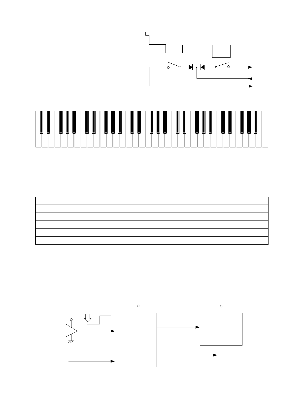
DAC (IC1: UPD6379GR)
The DAC receives 16-bit serial data output from the DSP. The data contains digital sound data of the
melody, chord, bass, and percussion for the right and left channels. The DAC converts the data into
analog waveforms and output them to each channel separately.
Synch signal
L OUT
R OUT
DAC
IC1
UPD6379GR
SI
LRCK
CLK
Data
Word clock
WCKO
Bit clock
SO
DSP
LSI2
HG51B277FB
SINC
SI
Word clock
WCKI
Bit clock
BCKI
Data
SCK1
SO
LRCK
BCK
CPU
LSI1
GT913F(T)
FILTER BLOCK
Since the sound signals from the DAC are stepped waveforms, the filter block is added to smooth the
waveforms.
AVDD
Q308
3.3K 4.7K 1K
R336
C343
2SC1740STPR
C123H
R334
680‰
C342
C821BA
1.5K
R335
AGAG
3.3K 4.7K 1K
R342 R343 R344
C346
C123H
C345
C821BA
R340
R337 R338
Q310
2SC1740STPR
1K
R339
AG
Q311
2SC1740STPR
1K
R345
22K
22K
AVDD
3.9K
R346
10K
R347
AG AG
R348R349
10V100
C348
50V22
C349
50V22
C350
From DAC
To main volume
6.3V220
AG
50V22
C340
50V22
C341
C339
Q309
2SC1740STPR
680‰
R341
1.5K
— 9 —
Page 12

POWER AMPLIFIER (IC301: TA8248K)
The power amplifier is a two-channel amplifier with standby switch.
The following table shows the pin function of IC301.
Pin No. Terminal In/Out Function
1 NC — Not used
2 B.S.2 — Terminal for a bootstrap capacitor
3 OUT2 Out Channel 2 output
4 VCC In +9 V source
5 OUT1 Out Channel 1 output
6 B.S.1 — Terminal for a bootstrap capacitor
7 Power GND In Ground (0 V) source
8 Stand by In Power control signal input. 0 V: Off, +9 V: On
9 DC — Terminal for a decoupling capacitor
10 NF1 In Negative feedback input
11 IN1 In Channel 1 input
12 IN2 In Channel 2 input
13 NF2 In Negative feedback input
14, 15 Pre GND In Ground (0 V) source
— 10 —
Page 13

ADJUSTMENT
DISPLAY PCB
1) Items to be adjusted:
Item Measuring Instrument
Vop voltage setting Voltmeter
2) Adjustment and Test Point Locations
(TOP VIEW)
VR501
(BOTTOM VIEW)
TP1
TP2
— 11 —
Page 14

3) Equipment connection/Procedure
Vop voltage setting
Set Voltmeter
Output
TP1-TP2
Input
Connection
Eye
62.23°
32.52°
LCD
Input
Point
(upper limit)
Eye
Input
Signal
Adjust
Output
Connection
Output
Point
Adjust for
VR501 Voltmeter TP1-TP2 Adjust for 4.2 to 4.3 V read-
ing on voltmeter under the
temparature 20 to 25 °C.
Make fine adjustment according to the following instruction.
1Watching the LCD at 32.52° angle to the horizontal, adjust Vop
voltage so that unenergized segments are seen dimly.
2Watching the LCD at 62.23° (upper limit) angle, check to see the
segments completely.
— 12 —
Page 15

MAJOR WAVEFORMS
1
2
CH1: 5 V–CH2: 5 V
1 NMI signal
JD connector pin 1
2 APO signal
JH connector pin 6
0.5 s
Power button ON
–
CH1
CH2
3
4
CH1: 5 V–CH2: 5 V
3 Button scan signal PA0
JD connector pin 9
4 Button scan signal PA1
JD connector pin 8
20 ms
–
CH1
CH2
9
0
CH1: 50 mV˜CH2: 50 mV
9 DAC output (L-ch)
JH connector pin 9
0 DAC output (R-ch)
JH connector pin 8
1 ms
1 ms
CH1
CH1
A
CH2
CH2
B
˜
CH1: 50 mV˜CH2: 50 mV
˜
A Sound signal (L-ch)
JK connector pin 4
B Sound signal (R-ch)
JK connector pin 5
5
6
CH1: 5 V–CH2: 5 V
5 Key scan signal KC0
JA connector pin 9
6 Key scan signal KC1
JA connector pin 10
50 µs
–
CH1
CH2
7
8
–
CH1: 5 V
7 RS signal PA4
JJ connector pin 4
8 R/W signal PA5
JJ connector pin 5
Power ON
CH2: 5 V
0.5 s
CH1
CH2
–
— 13 —
Page 16

PRINTED CIRCUIT BOARDS
Main PCB JCM454-MA1M
8
4
1
56
7
93
10
2
Top View
Bottom View
— 14 —
Page 17

Sub PCB KDM454-MA2M
12 11
— 15 —
Page 18

LCD PCB JCM454-LCD1M-A
Top View
Bottom View
— 16 —
Page 19

Main PCB JCM454-MA1M
SCHEMATIC DIAGRAMS
6
6
4
3
1
9
10
2
5 6
— 17 —
Page 20

Sub PCB KDM454-MA2M
12
11
— 18 —
Page 21

Display PCB JCM454-LCD1M
— 19 —
Page 22

Keyboard PCBs JCM617T-KY1M/KY2M
— 20 —
Page 23

PCBs JCM454-CN1M, JCM454-CN2M,JCM454-CN3M,JCM454-CN4M
— 21 —
Page 24

LCD
Common
2.738
(56.0) V.A.
(3.258)
4.625
5.26
cross-point
3-0.35
cross-point
cross-point
(121.0) V.A.
cross-point
cross-point
(4.595)
cross-point
cross-point
7-0.35
(5.26)
Segment
C13
C15
C16
C14
NCNCNC
NC
S2S3S4S5S6S7S8S9S10
S1
S11
S12
S13
S14
S15
S16
S17
S18
S19
S20
S21
S22
S23
S24
S25
S26
S27
S28
S29
S30
S31
S32
S33
S34
S35
S36
S37
S38
S39
S40C1C2C3C4C5C6C7C12
A
S17S8S9
S10
S32C9S33
S34
S35
S36
S37
S38
S39
S40S3C12S2S1
S11C9S12
C16
S29
C15
C14
C13
S30
S31
— 22 —
S32
C12
C11
C10
S20C9S19
NCNCNC
NC
NC
NCNCNC
S18
C13
C14
C15
C16
C10
C12
S21
NC
NC
NC
NC
C11
Page 25

LCD
Common
C13
C15
C16
C14
NC
NCNCNC
S2S3S4S5S6S7S8S9S10
S1
A
S11
S12
S13
S14
S15
S16
S17
S18
S19
S20
S21
S22
S23
S24
S25
S26
S27
S28
S29
S30
S31
S32
S33
S34
S35
S36
S37
S38
S39
S40C1C2C3C4C5C6C7C12
S17S8S9
S10
S32C9S33
Segment
5.5
66.0–0.2
9.087
S34
S35
S36
0.4
S37
S38
S39
S40S3C12S2S1
S11C9S12
C16
S29
C15
C14
C13
S30
S31
S32
125.0–0.2
0.4 0.4
0.4
0.4
C12
C11
C10
S20C9S19
NC
NCNCNC
NC
NCNCNC
0.4
S18
C13
C14
C15
C16
C10
C12
S21
NC
NC
NC
NC
0.4
0.15
0.2
C11
0.5
— 23 —
0.2
Page 26

EXPLODED VIEW
17
R-1
18
15
27
28
18
17
25
23
24
22
19
21
20
4
8
7
26
11
6
10
R-3
16
2
14
14
1
13
12
3
R-2
9
29
5
— 24 —
Page 27

PARTS LIST
CTK-631
Notes: This parts list does not include the cosmetic parts, which
parts are marked with item No. "R-X" in the exploded
view.
Contact our spare parts department if you need these
parts for refurbish.
1. Prices and specifications are subject to change without prior notice.
2. As for spare parts order and supply, refer to the
"GUIDEBOOK for Spare parts Supply", published
seperately.
3. The numbers in item column correspond to the same
numbers in drawing.
— 25 —
Page 28

PARTS PRICE LIST
CODE NO.
NAME
RICE CODE
1 6927 4340 PCB/ASSY(MA1M) M240991*1 1 DZ B
LSI1 2012 5005 LSI/CPU GT913F(T) 1 BO A
LSI2 2012 4494 LSI/DSP HG51B277FB-1 1 BF A
LSI3 2012 6336 LSI/ROM LH536PY8 1 BG A
LSI4/LSI5 2012 5572 LSI/RAM TC55257DFL-70L(EL) 2 AS A
IC1 2105 4746 IC UPD6379GR-E1 1 AO A
IC2 2012 1883 IC RN5VD40AA-TR 1 AE A
IC3 2105 3773 IC TC7SH08FU(TE85L) 1 AD A
X1 2590 2699 OSCILLATOR/CRYSTAL EF0B2005E0 1 AE B
X2 2590 2742 OSCILLATOR/CERAMIC AT-49-30M 1 AG B
2 6927 4370 PCB/ASSY(MA2M) M240992*1 1 DT B
IC301 2114 5775 IC TA8248K 1 BB A
IC302 2114 1421 IC/PHOTOCOUPLER PC900V 1 AK B
Q301/Q303 2250 1591 TRANSISTOR 2SB1237TV2R 2 AB A
Q306 2251 0672 TRANSISTOR 2SB1548-P.CS 1 AD A
Q305 2250 1593 TRANSISTOR 2SD1858TV2R 1 AB A
D301/D302 2390 3021 DIODE SRT14 2 AF B
Q307~Q313
D306 2360 1085 DIODE/ZENER HZS6B1LTD 1 AA B
D307 2360 3084 DIODE/ZENER HZS5.6NB3TD 1 AA A
D308 2360 3086 DIODE/ZENER HZS6C1LTD 1 AA A
J301 3501 7049 JACK/POWER HEC2305-01-330 1 AC A
J302 3612 0665 JACK/PHONE YKB21-5006 1 AG B
J303 3612 0789 JACK YKB21-5010 1 AC B
J304 3501 4816 JACK/DIN YKF51-5051 1 AH B
3 6927 4380 PCB/ASSY(LCD1M) M240993*1 1 DL B
LSI501 2012 6018 LSI/LCD DRIVER SED1278F2A 1 AV A
D501 2360 3056 DIODE/ZENER HZS6A2LTD 1 AA A
D502 2390 1344 DIODE 1SS133T-77 1 AA A
Q501/502 2253 0710 TRANSISTOR 2SD965-R(TA) 2 AB A
Q503 2250 1577 TRANSISTOR 2SA933ASTPR 1 AA A
Q504 2250 1592 TRANSISTOR 2SC1740STPR 1 AA A
T501 3012 1607 TRANSFORMER TE-CFL6-1M1 1 AL B
VR501 2775 0994 VOLUME EVND8AA03B53 1 AA A
4 6927 4390 PCB/ASSY(CN1234M) M140856*1 1 DA B
D601~D634 2390 1344 DIODE 1SS133T-77 34 AA B
LED601 2370 1414 LED MPR3338S-B149 1 AA B
VR601 2765 2213 VOLUME RS20H121-2KB 1 AD A
5 6927 4400 PCB/ASSY(KY1M) M140687*3 1 DA B
D501~D564 2301 0097 DIODE 1S2473 64 AA B
6 6927 4410 PCB/ASSY(KY2M) M140688*3 1 DA B
D565~D622 2301 0097 DIODE 58 AA B
7 6922 2720 WHITE KEY SET/LT M312118*1 4 AP A
8 6922 2730 WHITE KEY SET/LT M312118*2 1 AR A
9 6922 2740 BLACK KEY SET 10P M111726-1 2 AL A
10 6922 2750 BLACK KEY SET 5P M111726-2 1 AH A
N
11 6927 4260 RUBBER/CONTACT M340985*1 1 AS A
R-Rank
CTK-631
N ITEM
N
N
N
Q302,304,
N
N
PARTS
MAIN PCB
SUB PCB ASSY
2390 1344 TRANSISTOR 1SS133T-77 9 AA A
SPECIFICATION Q P
R
DISPLAY PCB
N
N
CONSOLE PCB
N
N
KEYBOARD PCB
N
N
KEYBOARD UNIT
Notes : Q-Quantity per unit
- 26 -
Page 29

PARTS PRICE LIST
CODE NO.
NAME
RICE CODE
12 6927 4690 RELECTOR M240939-1 1 AN B
13 3122 3701 CFL HMBV4BG2W147NLUAZG 1 AX B
14 6927 3420 HOLDER/CFL M440758-1 2 AA C
15 3335 6822 LCD LD-B10432E 1 CJ B
16 6927 3070 INTERCONNECTOR M440459-4 2 AO B
17 3831 1096 SPEAKER S12J89A 2 BH B
18 6927 6180 NET/SPEAKER M340981*1 2 BR X
19 6927 5090 RUBBER/BUTTON M240971-1 1 AE B
20 6927 4700 RUBBER/BUTTON M240942-1 1 AR B
21 6927 4710 RUBBER/BUTTON M240943-1 1 AP B
22 6927 4720 RUBBER/BUTTON M240944-1 1 AR B
23 6927 5100 RUBBER/BUTTON M240945-1 1 AS B
24 6927 5110 RUBBER/BUTTON M240946-1 1 AI B
25 6927 5120 RUBBER/BUTTON M240947-1 1 AI B
26 6927 0510 SWITCH/SLIDE KNOB CSB-08D 1 AD B
27 6921 5030 KNOB/SLIDE M311859-1 2 AA B
28 6927 7240 PLATE/DISPLAY M341032*1 1 BC C
29 6918 1630 COVER/BATTERY M311164*1 1 AT B
N 6926 9590 STAND/NOTE M340876*1 1 BK B
R-Rank
CTK-631
N ITEM
N
N
N
N
N
N
N
N
N
N
N
PANEL UNIT
ACCESSORY
PARTS
SPECIFICATION Q P
R
Notes : Q-Quantity per unit
- 27 -
Page 30

CASIO TECHNO CO.,LTD.
Overseas Service Division
Nishi-Shinjuku Kimuraya Bldg. 1F
5-25, Nishi-Shinjuku 7-Chome
Shinjuku-ku, Tokyo 160-0023, Japan
 Loading...