Page 1

CTK-6300IN
JUL. 2012
Ver. 2 : Feb. 2013
Page 2

CTK-6300IN
CONTENTS
SPECIFICATIONS ........................................................................................... 1
BLOCK AND WIRING DIAGRAM .................................................................. 3
PCB INFORMATION ....................................................................................... 4
CIRCUIT DESCRIPTION ................................................................................ 5
PRINTED CIRCUIT BOARDS ......................................................................... 7
DISASSEMBLY ............................................................................................. 10
DIAGNOSTIC PROGRAM ............................................................................ 31
EXPLODED VIEW ......................................................................................... 39
PARTS LIST .................................................................................................. 41
SCHEMATIC DIAGRAMS ............................................................................. 45
Page 3

SPECIFICATIONS
Keyboard 61 standard-size keys
Touch Response 2 types, Off
Maximum Polyphony 48 notes (24 for certain tones)
Tones
Built-in Tones 700
User Tones Up to 10 (Tone Editor)
Functions Layer, Split
Reverb 1 to 10, Off
Chorus 1 to 5, Off
DSP
Preset DSP 100
User DSP Up to 100
Metronome
Beats per Measure 0, 2 to 6
Tempo Range 30 to 255
CTK-6300IN
Auto Accompaniment
Built-in Rhythms 210
User Rhythms Up to 10 (Rhythm Editor)
Demo Songs 5 songs
Registration 32 (4 setups × 8 banks)
Song Sequencer Real-time recording, playback
Keyboard Play 5 songs, 17 tracks
Memory Capacity Approximately 12,000 notes (total for 5 songs)
Mixer 32 parts (A01-A16/B01-B16)
Master parameters, DSP parameters, Part parameters
Other Functions
Transpose ±1 octaves (–12 to +12 semitones)
Octave Shift UPPER 1/UPPER 2/LOWER, ±2 octaves
Tuning A4 = 415.5 - 440.0 - 465.9 Hz
Scale Tuning Scale Fine Tune, Preset Scales
Music Preset 305 built-in, plus 50 user presets
One Touch Preset 210
Auto Harmonize 12 types
Arpeggiator 150 types
Equalizer 5 presets
MIDI 16 multi-timbre received, GM Level 1 standard
Pitch Bend Wheel
Pitch Bend Range 0 to 24 semitones
Memory Cards
Supported Memory Cards SD or SDHC memory cards, 32 GB or less
Functions SMF playback, le storage, le recall, le delete, card format
– 1 –
Page 4

CTK-6300IN
Inputs/Outputs
USB jack TYPE B
Sustain/Assignable jack Standard jack (sustain, sostenuto, soft, start/stop)
Phones jack Stereo standard jack
Line Out R, L/MONO jacks Standard jack × 2
Output Impedance: 2.3 kΩ, Output Voltage: 1.5 V (RMS) MAX
Audio In jack Stereo mini jack
Input Impedance: 9 kΩ, Input Sensitivity: 200 mV
Power Jack 12 V DC
Power Supply 2-way
Batteries 6 D-size zinc-carbon batteries or alkaline batteries
Battery Life Approximately 4 hours continuous operation on alkaline batteries
AC Adaptor AD-A12150LW
Auto Power Off Approximately 6 minutes after last key operation (during battery use),
approximately 4 hours after last key operation (during AC adaptor use)
Speakers 12 cm × 2 + 3 cm × 2 (Output: 6.0 W + 6.0 W)
Power Consumption 12 V 18 W
Dimensions 94.8 × 38.4 × 12.2 cm (37 3/8 × 15 1/8 × 4 13/16 inch)
Weight Approximately 5.7 kg (12.6 lbs) (without batteries)
– 2 –
Page 5
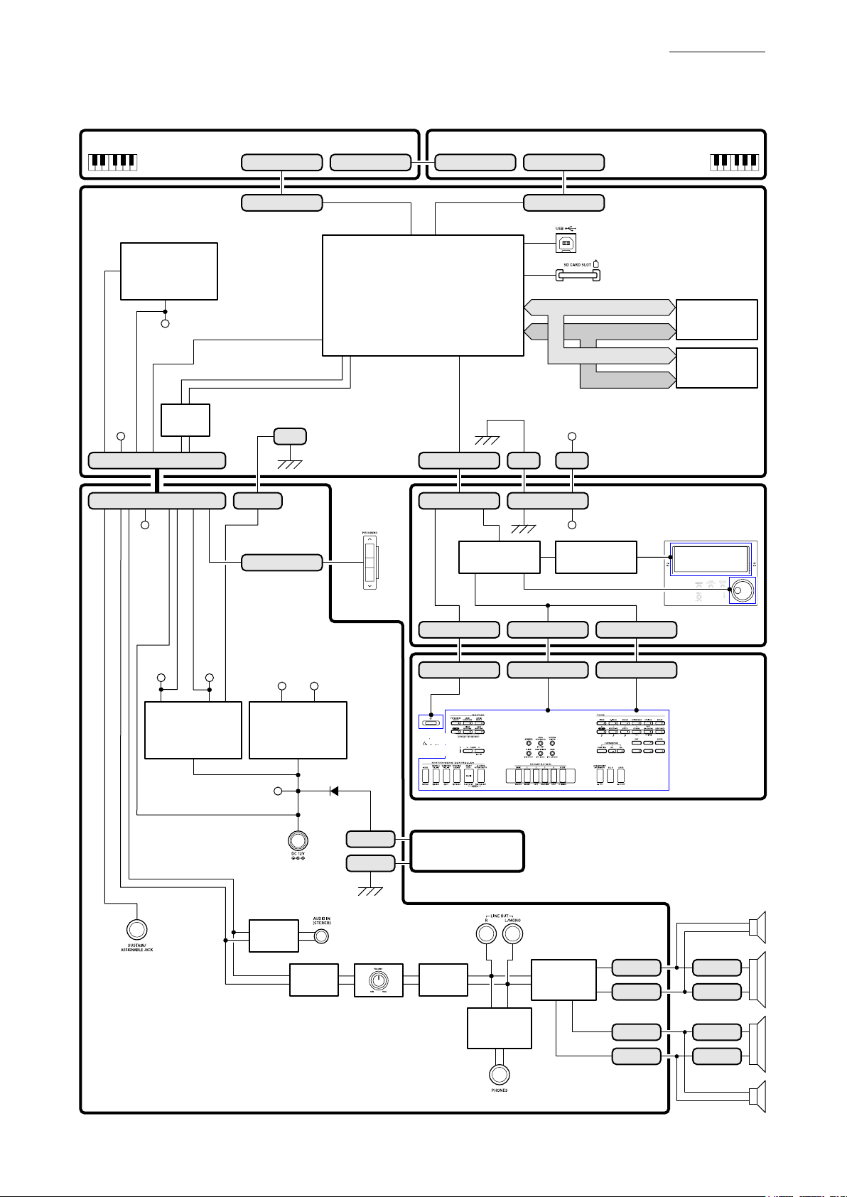
BLOCK AND WIRING DIAGRAM
CTK-6300IN
KEYBOARD PCB (M802-KYA1)
MAIN PCB
(M842-MDA1)
Power Supply Circuit
VD5
IC6, FU1, C24,
C25, C27, C33,
C35, C167
SWVP, MUTE, BEND
PAD (Y)CN15 (14 pin)
VA5
CN1 (14 pin)
VD3
VD3
Filter
IC5
CN801 (13 pin)
CN2 (13 pin)
PEDAL, APO,
SPMUTE, ADIN,
CN15
CN7 (3 pin)
CN802 (10 pin)
FI0~FI3,
SI0~SI3, KC0~KC4
LOUT
ROUT
PITCH BEND
CN803 (10 pin)
FI4~FI7,
SI4~SI7, KC5~KC7
MPU
IC7
CN10 (8 pin)
CN9 (8 pin)
CN14
CN1 (2 pin)
Button/LED/LCD
Controller IC1
CN804 (11 pin)
CN3 (11 pin)
USB (CN7)
VD5
CN13
VD5
LCD Driver
KEYBOARD PCB (M802-KYA2)
SD (CN12)
MA1~MA19
MD0~MD15
MA1~MA23
MD0~MD15
SRAM
(4 Mbit)
IC9
Flash Memory
(128 Mbit)
IC11
CONSOLE PCB
(M842-LCA1)
IC2
LCD
Power Supply Circuit
IC2, C56, C59,
C60, C62, C67,
C68, C76, D4
SUSTAIN/
ASSIGNABLE
(J9)
POWER & AMP PCB
(M842-PSA1)
VA5VD5
VCP
LOUT ROUT
VA9VC
Power Supply Circuit
Q1, Q2, Q3,
C7, C9
D1
ADIN
DC 12 V
(J2)
Filter
IC3
AUDIO IN
(J7)
Filter
IC6
CN1 (+)
CN2 (-)
MAIN VOL.
(VR2)
CN3 (4 pin)
CN2 (4 pin)
POWER
POWER
SIWTCH
SIWTCH
BATTERY
Filter
IC5
PHONES
Headphones
Amplifier
IC8
(J3)
CN5 (15 pin)
CN5 (15 pin)
BUTTON & LED
LINE OUT
(J5, J4)
Power
Amplifier
IC1
CN7 (3 pin)
CN7 (3 pin)
CN11 (+)
CN12 (-)
CN5 (+)
CN6 (-)
DIAL
CONSOLE PCB
(M842-CNA1)
BUZZER (R)
SPEAKER (R)
RSP (+)
RSP (-)
LSP (+)
LSP (-)
SPEAKER (L)
BUZZER (L)
– 3 –
Page 6

PCB INFORMATION
M842-PSA1
M842-LCA1 M842-MDA1
CTK-6300IN
M802-KYA1 M842-CNA1
Parts Name PCB Name Components
Main PCB
, SRAM (4 Mbit), Flash Memory (128 Mbit),
PCB UNIT/MAIN M842-MDA1
Power & Amp PCB
PCB UNIT/POWER & AMP M842-PSA1
Console PCB
PCB UNIT/LCA1 M842-LCA1 Button/LED/LCD Controller, LCD Driver, LCD, Dial
PCB UNIT/CNA1 M842-CNA1 Power Switch, Buttons, LED
Keyboard PCB
PCB UNIT/KEYBOARD/KYA
M802-KYA1
M802-KYA2
MPU
Power Supply Circuit, Filter, SD card slot, USB port
Power Supply Circuit, Power Ampli er,
Headphones Ampli er, Filters, Main Volume, Speaker,
Buzzer, Pitch Bend, DC 12 V Terminal, AUDIO IN Jack,
LINE OUT (R, L/MONO) Jacks, PHONES Jack,
SUSTAIN/ASSIGNABLE Jack
Keyboard
M802-KYA2
– 4 –
Page 7
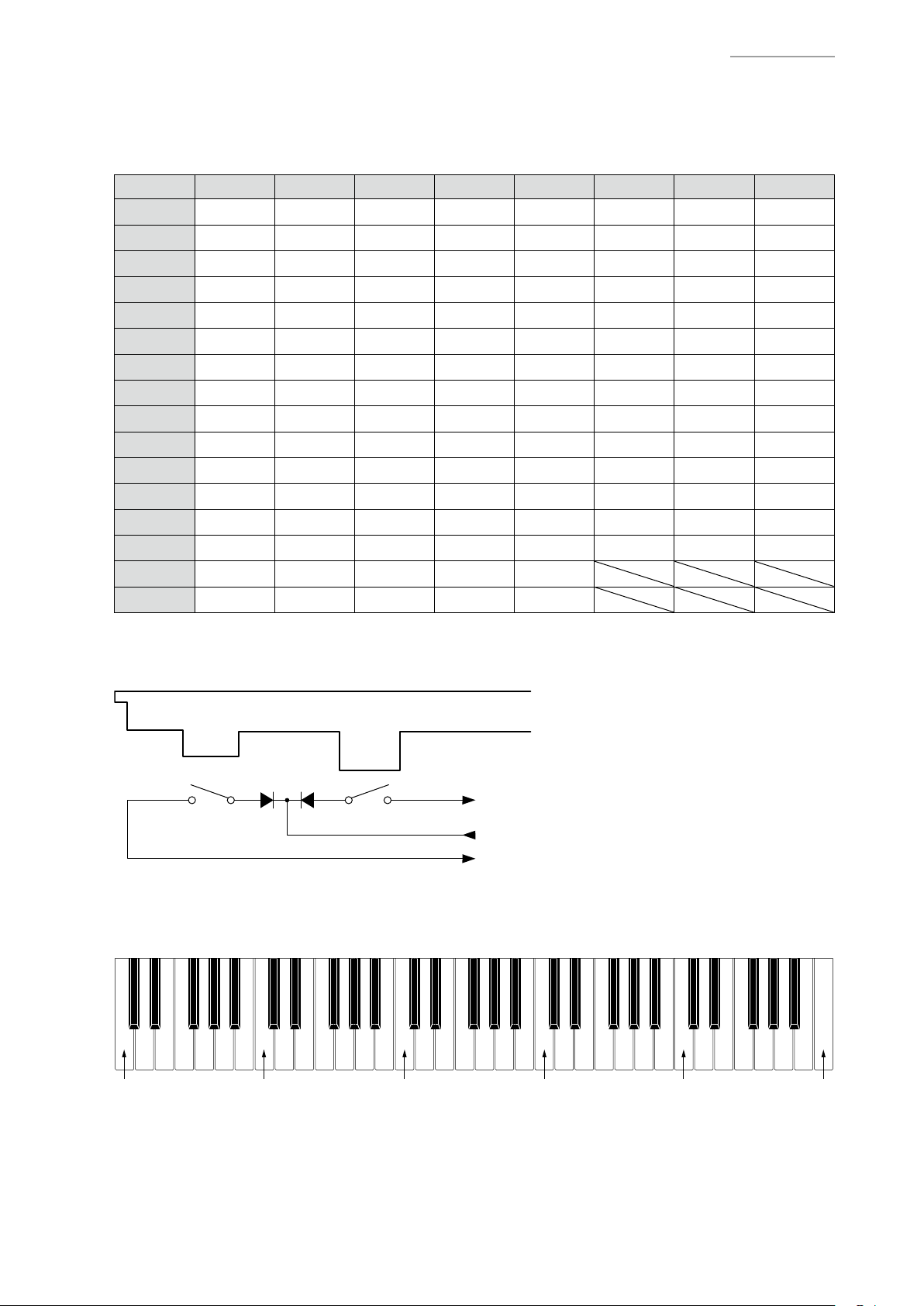
KEY MATRIX
KC0 KC1 KC2 KC3 KC4 KC5 KC6 KC7
FI0 C2
SI0 C2
FI1 G2#
SI1 G2#
FI2 E3
SI2 E3
FI3 C4
SI3 C4
FI4 G4#
SI4 G4#
FI5 E5
SI5 E5
FI6 C6
SI6 C6
FI7 G6#
SI7 G6#
1
2
1
2
1
2
1
2
1
2
1
2
1
2
1
2
CIRCUIT DESCRIPTION
C2#
C2#
A2
A2
F3
F3
C4#
C4#
A4
A4
F5
F5
C6#
C6#
A6
A6
1
2
1
2
1
2
1
2
1
2
1
2
1
2
1
2
D2
D2
A2#
A2#
F3#
F3#
D4
D4
A4#
A4#
F5#
F5#
D6
D6
A6#
A6#
1
2
1
2
1
2
1
2
1
2
1
2
1
2
1
2
D2#
D2#
B2
B2
G3
G3
D4#
D4#
B4
B4
G5
G5
D6#
D6#
B6
B6
1
2
1
2
1
2
1
2
1
2
1
2
1
2
1
2
E2
E2
C3
C3
G3#
G3#
E4
E4
C5
C5
G5#
G5#
E6
E6
C7
C7
1
2
1
2
1
2
1
2
1
2
1
2
1
2
1
2
F2
F2
C3#
C3#
A3
A3
F4
F4
C5#
C5#
A5
A5
F6
F6
1
2
1
2
1
2
1
2
1
2
1
2
1
2
CTK-6300IN
F2#
1
F2#
2
D3
1
D3
2
A3#
1
A3#
2
F4#
1
F4#
2
D5
1
D5
2
A5#
1
A5#
2
F6#
1
F6#
2
G2
G2
D3#
D3#
B3
B3
G4
G4
D5#
D5#
B5
B5
G6
G6
1
2
1
2
1
2
1
2
1
2
1
2
1
2
Each key has two contacts, the rst contact 1 and second contact 2.
NOTE: The diagram below illustrates how the contacts work.
Key
FI
Second contact
NOMENCLATURE OF KEYS
C2 C3 C4 C5 C6 C7
First contact
KC
SI
– 5 –
Page 8
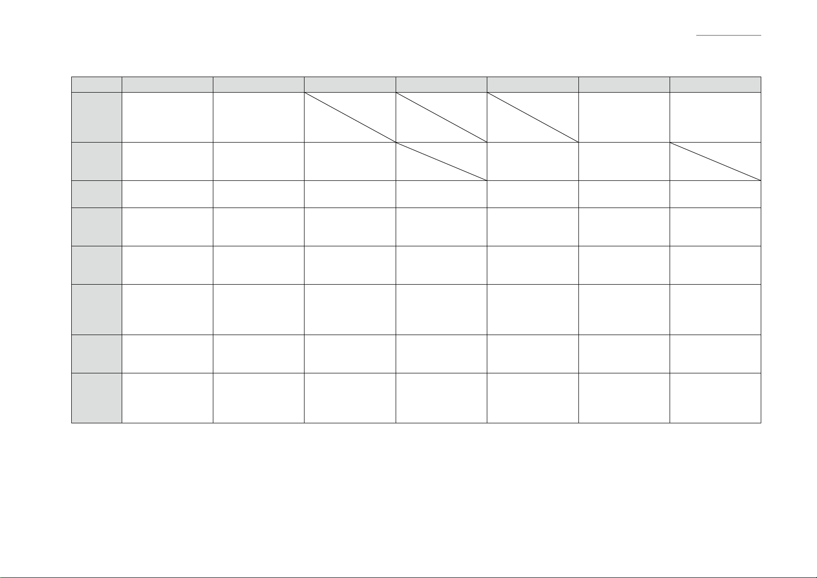
BUTTON MATRIX
KC0 KC1 KC2 KC3 KC4 KC5 KC6
ACCOMP ON/OFF,
CHORDS,
KI0
KI1
KI2
KI3
KI4
KI5 TEMPO
KI6
KI7
$
PART SELECT,
DEMO
SYNCHRO/
ENDING,
PAUSE
NORMAL/FILL-IN,
REW
s
4,
STEP
[C]
LATIN/WORLD
[D]
INDIAN,
MUSIC PRESET
2,
COPY
w
VARIATION/
FILL-IN,
FF
d
START/STOP,
PLAY/STOP,
DEMO
CARD,
LOAD/SAVE
#
3,
QUANTIZE
[F]
USER RHYTHMS
[E]
PIANO RHYTHMS,
ONE TOUCH
PRESET
[A]
POPS/ROCK/
DANCE
1,
INSERT
INTRO,
REPEAT
STORE,
MENU
#
MIXER,
EFFECT
#
TEMPO q,
TAP
#
[B]
JAZZ/
EUROPEAN
METRONOME,
BEAT
$
BANK,
DELETE
ENTER
u
EXIT
t
NO/–,
TRANSPOSE
#
AUTO
HARMONIZE/
ARPEGGIATOR,
TYPE
$
TONE EDITOR,
SCALE
#
y i
LAYER,
OCTAVE
$
[L]
USER TONES
[I]
SYNTH,
8
[H]
REED/PIPE,
7
FUNCTION
RECORD
RHYTHM EDITOR
[E]
STRINGS,
REST
[K]
GM/DRUMS,
.
[J]
OTHERS,
,
SPLIT
[G]
INDIAN,
6
CTK-6300IN
SONG
SEQUENCER,
EDIT
#
[F]
BRASS
YES/+,
TRANSPOSE
#
[D]
GUITAR/BASS,
•
[C]
ORGAN,
2
[B]
E. PIANO,
1
[A]
PIANO,
5
– 6 –
Page 9

PRINTED CIRCUIT BOARDS
Main PCB: M842-MDA1 Power & Amp PCB: M842-PSA1 Console PCB: M842-LCA1
CTK-6300IN
– 7 –
Page 10

Console PCB: M842-CNA1
CTK-6300IN
– 8 –
Page 11

Keyboard PCB: M802-KYA1
CTK-6300IN
Keyboard PCB: M802-KYA2
– 9 –
Page 12

CTK-6300IN
DISASSEMBLY
CAUTION
z
The photos show a prototype. The appearance of the instrument, such as color, may
differ from the actual model.
z
To avoid damages to the instrument and the oor, lay the instrument on a mattress
or blanket before starting disassembling.
z
There are several kinds of screws. Be sure to use the correct type of screws when
reassembling. It is advisable to sort the screws as shown below after removing
them.
z
If a screw cap is attached to a screw, be sure to reattach the screw cap when
reassembling.
BEFORE STARTING REPAIR OR SERVICING
z
Remove the AC adaptor, AC cord or batteries.
z
Remove accessories such as the music stand.
– 10 –
Page 13

DISASSEMBLY PROCEDURE
A. REMOVE THE PANEL UNITS
Left panel unit &
Sub panel unit
Main panel unit Right panel unit
CTK-6300IN
A-1. Undo 21 or seven screws on the bottom surface of the main unit.
NOTE: To remove only the main panel unit, undo seven screws indicated with red circles in the
illustration below.
– 11 –
Page 14
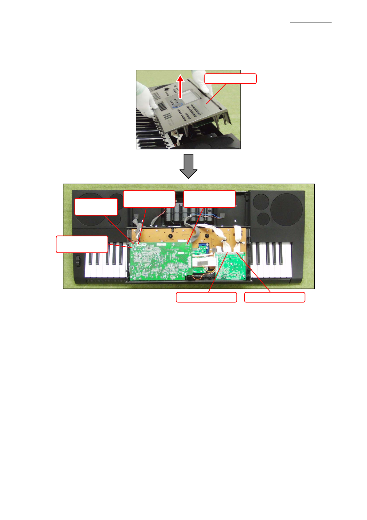
A-2. Place the main unit with the keys facing up.
A-3. Lift the main panel unit and turn it over.
NOTE: The main panel unit is connected to the lower case unit with the lead wires and FFCs.
Use caution when turn over the main panel unit.
Main panel unit
CTK-6300IN
Lead wires
(Batteries)
Lead wires
(Left SPEAKER)
FFC
(BENDER-UNIT)
Lead wires
(Right SPEAKER)
FFC (M802-KYA1) FFC (M802-KYA2)
– 12 –
Page 15

A-4. Unsolder six lead wires and three FFCs.
A-5. Remove the main panel unit.
CTK-6300IN
Lead wire (Red)
Lead wire (Green)
Lead wire (Black)
FFC (BENDER-UNIT)
Lead wire (White)
Lead wire (Brown)
Lead wire (Blue)
Cable tie
FFC (M802-KYA1)
FFC (M802-KYA2)
Main panel unit
– 13 –
Page 16
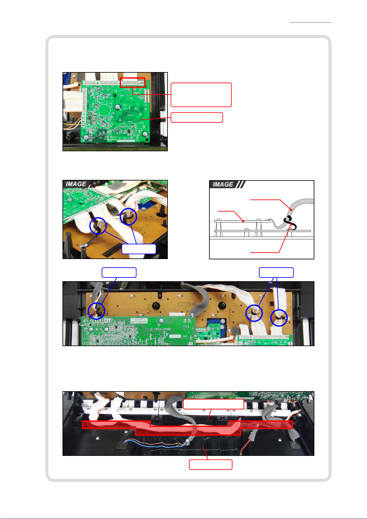
CTK-6300IN
<Notes On Assembly>
• The number of pins on the PCB pad differs from that on the cable. Solder in the way that No.1
pin on the cable (orange) is connected to No.1 pad on the PCB.
FFC (M802-KYA2)
PCB: 15 pads
Cable: 11 pins
M842-MDA1 PCB
• Use the wire clip as shown in the illustration below to arrange the position of the FFCs and the
lead wires in a way that they are upright against the PCB.
Cables
PCB
Wire clips
Wire clip Wire clips
Wire clip
• Arrange the FFCs and lead wires so that they are positioned in the space indicated with a red
rectangle in the photo below.
NOTE: Arrange the FFCs and lead wires between the battery box and the case (keyboard
side).
Case (Keyboard side)
Battery box
– 14 –
Page 17

CTK-6300IN
A-6. Undo 10 screws and then remove the left panel unit, right panel unit and sub panel unit.
NOTE: To remove only the left panel unit, undo six screws indicated with red circles and green
circles in the illustration below.
NOTE: To remove only the right panel unit, undo four screws indicated with blue circles in the
illustration below.
NOTE: To remove only the sub panel unit, undo two screws indicated with green circles in the
illustration below.
Cable tie
Sub panel unit
Left panel unit Right panel unit
– 15 –
Page 18

B. REMOVE THE M842-MDA1 PCB
B-1. Unsolder two FFCs and three lead wires.
B-2. Undo three screws and then remove the M842-MDA1 PCB.
FFC (M842-PSA1) FFC (M842-LCA1)
Lead wire
(Orange)
Lead wire
(White)
M842-MDA1 PCBLead wire (Yellow)
CTK-6300IN
<Notes On Assembly>
• The number of pins on the PCB pad differs from that on the cable. Solder in the way that No.1
pin on the cable (orange) is connected to No.1 pad on the PCB.
M842-MDA1 PCB
FFC (M842-PSA1)
PCB: 16 pads
Cable: 14 pins
C. REMOVE THE M842-PSA1 PCB
C-1. Remove the KNOB/ROTARY.
KNOB/ROTARY
– 16 –
Page 19

C-2. Unsolder one FFC and one lead wire.
C-3. Undo six screws and then remove the M842-PSA1 PCB.
M842-PSA1 PCB
SPONGE
CTK-6300IN
FFC (M842-PSA1)
M842-MDA1 PCB
Lead wire (Yellow)
<Notes On Assembly>
• The number of pins on the PCB pad differs from that on the cable. Solder in the way that No.1
pin on the cable (orange) is connected to No.1 pad on the PCB.
M842-MDA1 PCB
FFC (M842-PSA1)
PCB: 16 pads
Cable: 14 pins
– 17 –
Page 20
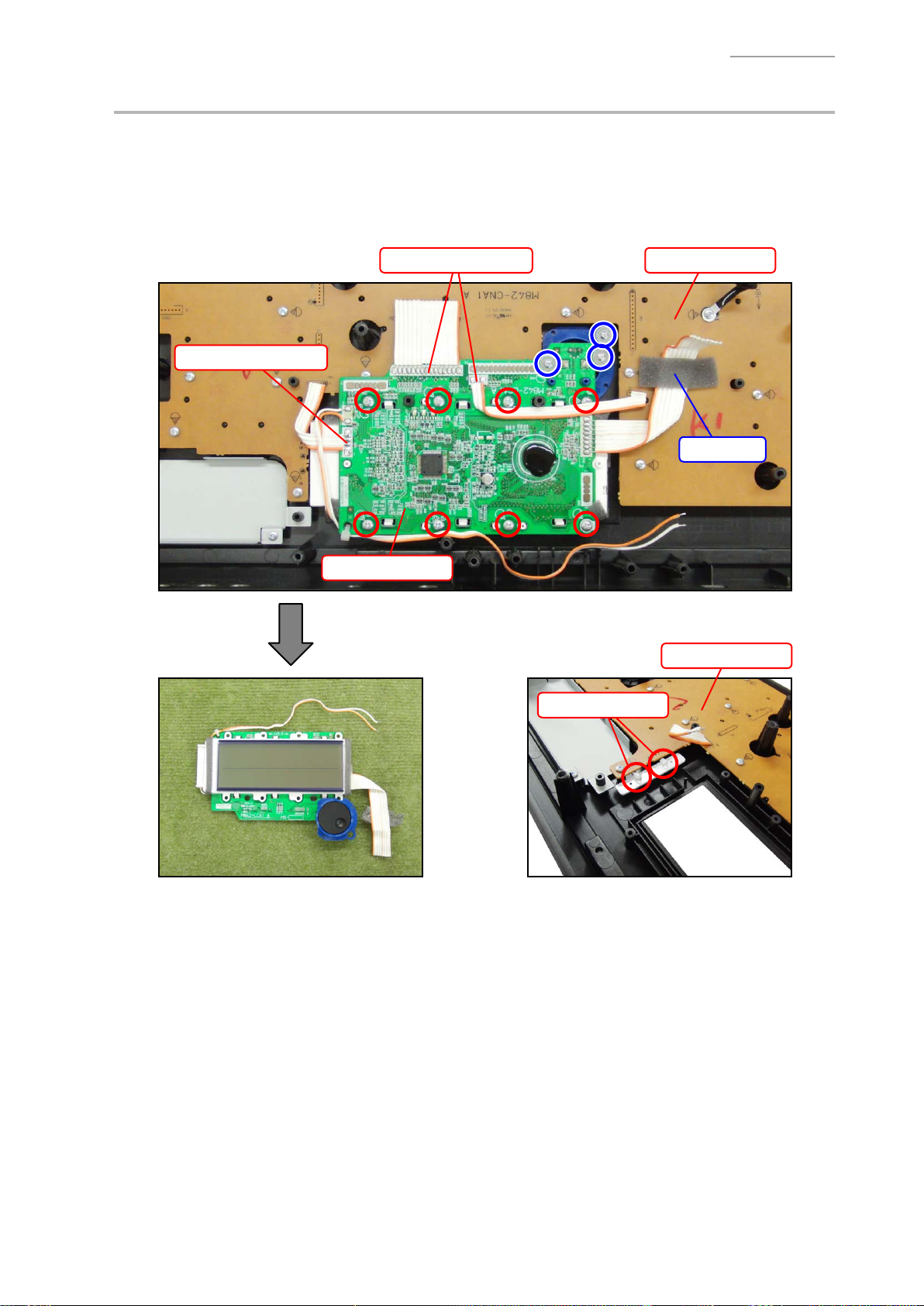
CTK-6300IN
D. REMOVE THE M842-LCA1 PCB
NOTE: The backlight LED for the LCD is not mounted on the M842-LCA1 PCB. The LED is mounted on
the M842-CNA1 PCB.
D-1. Unsolder three FFCs.
D-2. Undo 11 screws and remove the M842-LCA1 PCB together with the backlight unit and dial.
NOTE: There are two types of screws. Be sure to use the correct screw when reassembling.
FFC (M842-CNA1)
FFCs (M842-CNA1)
M842-LCA1 PCB
M842-CNA1 PCB
SPONGE
S
M842-CNA1 PCB
Backlight LEDs
– 18 –
Page 21

CTK-6300IN
<Notes On Assembly>
• Assemble the LCD into the case before assembling the M842-LCA1 PCB. In doing so, be sure
that the LCD is assembled in the correct orientation.
NOTE: When assembling the LCD and M842-LCA1 PCB, make sure that the LCD surfaces
are free from dust and dirt.
LCD
Align the protrusion.
• To install the M842-LCA1 PCB, tighten the screws for the LCD part in the order indicated with
the numbers below. If not tighten correctly, it may cause the LCD display errors.
8 2 4 6
M842-LCA1 PCB
7 3 1 5
D-3. Remove the LCD and two RUBBER-CONNECTOR/LCDs.
LCD
RUBBER-CONNECTOR/LCDs
– 19 –
Page 22

D-4. Remove the KNOB/DIAL and BEZEL/DIAL.
Press lightly.
D-5. Disengage six hooks and then remove the M842-LCA1 PCB and backlight unit.
M842-LCA1 PCB
CTK-6300IN
BEZEL/DIALKNOB/DIAL
Backlight unit
– 20 –
Page 23

CTK-6300IN
E. DISASSEMBLY OF THE BACKLIGHT UNIT
NOTE: The backlight LED for the LCD is not mounted on the backlight unit. The LED is mounted on the
M842-CNA1 PCB.
E-1. Remove two SPONGEs and then remove the TOP-PIECE, FILM, BACK-LIGHT-PLATE and
REFLECTOR.
SPONGEs
SPONGEs
TOP-PIECE
BACK-LIGHT-PLATE
REFLECTOR
FILM
– 21 –
Page 24

<Notes On Assembly>
SPONGESPONGE
• Assemble the components for the backlight unit as illustrated below.
TOP-PIECE
FILM
CTK-6300IN
Incline
Rough surface
BACK-LIGHT-PLATE
Flat surface
REFLECTOR
Fit the hole in the FILM
over the projection.
– 22 –
Page 25

CTK-6300IN
F. REMOVE THE M842-CNA1 PCB
F-1. Undo 22 screws and then remove the M842-CNA1 PCB and RUBBER-BUTTONs.
NOTE: Handle the M842-CNA1 PCB carefully, for the backlight LED for the LCD is mounted on it.
Wire clip Wire clips
Backlight LEDs
M842-CNA1
PCB
– 23 –
Page 26

<Caution When Replacing With A New Parts>
• Mount the LED as shown below while paying attention to the polarity.
D8
CTK-6300IN
10.7 ± 0.5 mm
D8
0.94 ± 0.3 mm
D9
10.7 ± 0.5 mm
D9
0.35 ± 0.3 mm
<Notes On Assembly>
• When assembling with the screws, be sure to tighten them together with coating clips.
– 24 –
Page 27

CTK-6300IN
G. REMOVE THE BENDER-UNIT
NOTE: Neither the M842-CNA2 PCB nor M842-CNA3 PCB functions as a circuitry board; the CNA3
PCB is used to hold wires in place.
G-1. Undo two screws and then remove the M842-CNA2 PCB.
G-2. Undo three screws and then remove the M842-CNA3 PCB.
M842-CNA2 PCB
M842-CNA3 PCB
G-3. Undo two screws and then remove the BENDER-UNIT.
BENDER-UNIT
FABRIC-TAPEs
<Notes On Assembly>
• Before assembling the M842-CNA3 PCB, be sure that the fold of the FFC is NOT placed on top
of the rib.
OK NG
– 25 –
Page 28
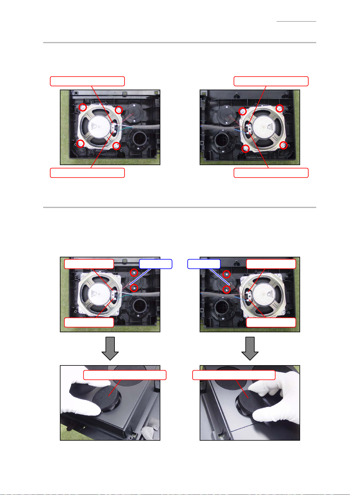
H. REMOVE THE SPEAKER
H-1. Unsolder four lead wires.
H-2. Undo four screws and then remove the SPEAKER.
<Left SPEAKER> <Right SPEAKER>
CTK-6300IN
Lead wires (Red & White)
Lead wires (Black & Green)
Lead wires (Black & Brown)
Lead wires (Red & Blue)
I. REMOVE THE BUZZER (TWEETER)
I-1. Unsolder two lead wires.
I-2. Undo two screws and then remove the SPEAKER-COVER/TWEETER.
NOTE: In case the SPEAKER-COVER/TWEETER does not come off easily, insert tweezers in
the screw hole and press the part lightly from inside.
<Left BUZZER> <Right BUZZER>
Lead wire (Red)
Lead wire (Black)
PACKING PACKING
SPEAKER-COVER/TWEETERSPEAKER-COVER/TWEETER
Lead wire (Black)
Lead wire (Red)
– 26 –
Page 29
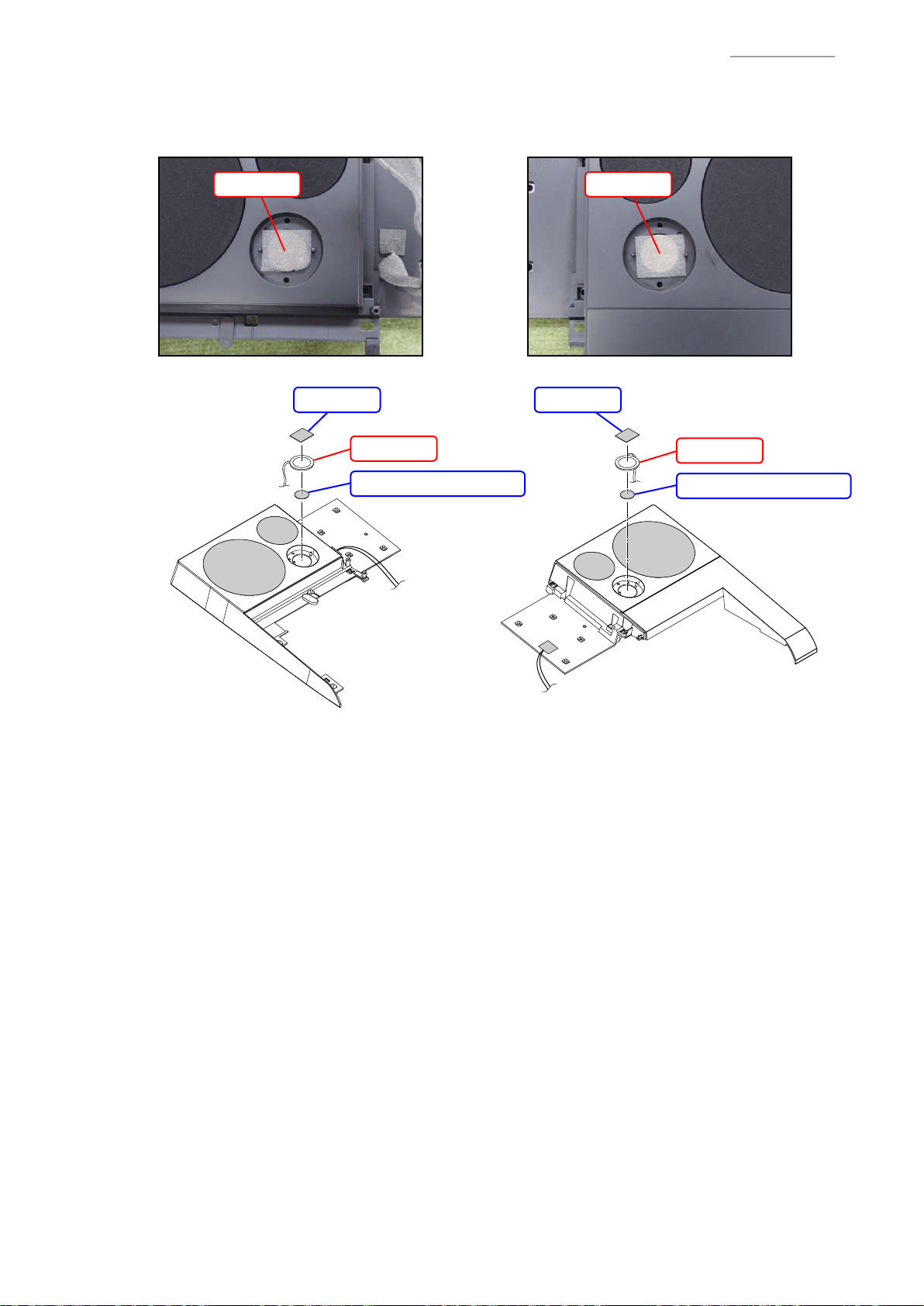
I-3. Remove the BUZZER.
NOTE: It is secured with the DOUBLE-FACED-TAPE.
<Left BUZZER> <Right BUZZER>
BUZZER BUZZER
CTK-6300IN
SPONGE
BUZZER
DOUBLE-FACED-TAPE
SPONGE
BUZZER
DOUBLE-FACED-TAPE
– 27 –
Page 30

J. REMOVE THE KEYBOARD
J-1. Undo 21 screws and then remove the KEYs.
CTK-6300IN
– 28 –
Page 31

K. REMOVE THE M802-KYA1/KYA2 PCBs
M802-KYA1 PCB M802-KYA2 PCB
K-1. Disengage the hooks and then remove the M802-KYA1/KYA2 PCBs.
CTK-6300IN
– 29 –
Page 32

K-2. Remove ve RUBBER-CONTACTs.
NOTE: One RUBBER-CONTACT differs in length.
RUBBER-CONTACTs
CTK-6300IN
This RUBBER-CONTACT differs
from the others in length.
<How To Install RUBBER-CONTACT>
• Lightly insert the tip of a RUBBER-CONTACT into the
PCB. Pull the tip from the back of the PCB and
install it using a tool such as tweezers. Do not
forcibly pull it.
– 30 –
Page 33
DIAGNOSTIC PROGRAM
PREPARATION
(1) Connect the AC adaptor.
NOTE: “AC ADAPTOR CHECK” cannot be performed unless the AC adaptor is connected.
(2) Turn the main volume to the maximum.
(3) Insert an SD card into the card slot.
NOTE: Use an SD card or SDHC card with a capacity of 32 GB or less.
NOTE: “SD CARD CHECK” cannot be performed unless the card is inserted.
(4) Have a PC and a USB cable ready.
NOTE: “USB CHECK” cannot be performed without a PC and a USB cable.
Operating System:
• Windows® XP (SP2 or later) *1 / Windows Vista® *2 / Windows® 7 *
• Mac OS® X (10.3.9, 10.4.11, 10.5.X, 10.6.X, 10.7.X)
*1: Windows XP Home Edition / Windows XP Professional (32 bit)
*2: Windows Vista (32 bit)
*3: Windows 7 (32 bit, 64 bit)
3
CTK-6300IN
HOW TO START THE DIAGNOSTIC PROGRAM
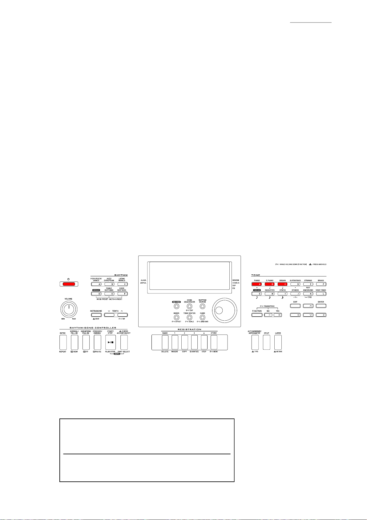
(1) Hold down the “TONE [A]”, “TONE [B]” and “TONE [C]” buttons at the same time, to turn the power
ON.
NOTE: BesuretoturnOFFthepowerwhenthetestisnished.
(2) Release the “TONE [A]”, “TONE [B]” and “TONE [C]”
(3) Once the diagnostic program is launched, “MODEL CHECK” and “SUB CPU CHECK” are performed
automatically, and then the result is displayed.
<Testing Main Screen>
NOTE: After the test is performed even once, the “SUB CPU CHECK” result will not be displayed
on the LCD.
buttons.
TESTCTK6300I
SubCPU: OK
– 31 –
Page 34
CTK-6300IN
TEST ITEMS
Pressing a test button while on the main screen enables the corresponding test item to be tested.
Test Items Buttons Note
A. BUTTON CHECK TONE [A]
B. LED CHECK TONE [L]
C. LCD CHECK TONE [B]
D. ROM CHECK TONE [E]
E. RAM CHECK TONE [F]
F. ROM VERSION CHECK TONE [I]
G. SD CARD CHECK TONE [G] SD card
H. USB CHECK TONE [H] PC, USB cable
I. AC ADAPTOR CHECK TONE [K] AC adaptor
TEST PROCEDURE
A. BUTTON CHECK
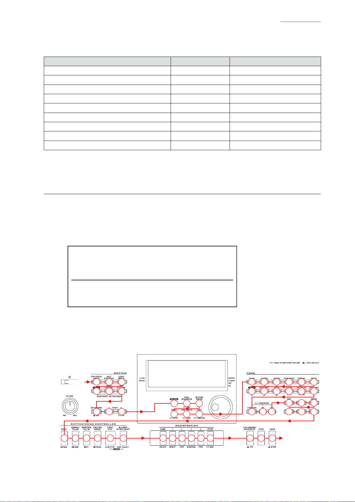
A-1. Press the “TONE [A]” button to select the “BUTTON CHECK”.
A-2. Press the button in the order indicated in the illustration below.
If the result passes (OK):
• Theconrmationchordsoundsand“00XX”isdisplayedontheLCDwith“XX”indicatingthe
corresponding button number in the illustration below.
SW
00XX
If the result fails (NG):
• If there is a button failure or the buttons are pressed in a wrong sequence, an error tone sounds
and the button number which you pressed will be displayed on the LCD.
<Main panel>
START
START
43 46 48
0C 0E0D
0F 11
10
4B 4A
49
474544
1B 1D 1C
1F 1E 1A
12 14 15 16 17
– 32 –
00 0504030201
06 0B0A090807
25
2A
24 23 28
22
2B 2C
13
2D
TO PITCH BEND
TO PITCH BEND
29
26
27
Page 35

<Pitch Bend> <Dial>
CONTINUEDCONTINUED
9D 9B 9C 9B B1 B2
Turn right Turn left
SW TEST OK!
CTK-6300IN
FINISH
FINISH
Turn up
Move back
to the center
Turn down Move back
to the center
A-3. Whenyouturnthedialattheend,aconrmationchordsoundsand“SWTESTOK!”isdisplayed
on the LCD.
A-4. Check to see if the LCD is as shown below.
SW TEST OK!
00B2
A-5. Press the “RHYTHM [A]” button to return to the main screen.
B. LED CHECK
B-1. Press the “TONE [L]” button to perform the “LED CHECK”.
B-2. Check to see if the LEDs indicated below are lit.
• Lit in blue: START/STOP
• Lit in red: RECORD
B-3. Press the “RHYTHM [A]” button to return to the main screen.
NOTE: All LEDs turn off when you return to the main screen.
– 33 –
Page 36
C. LCD CHECK
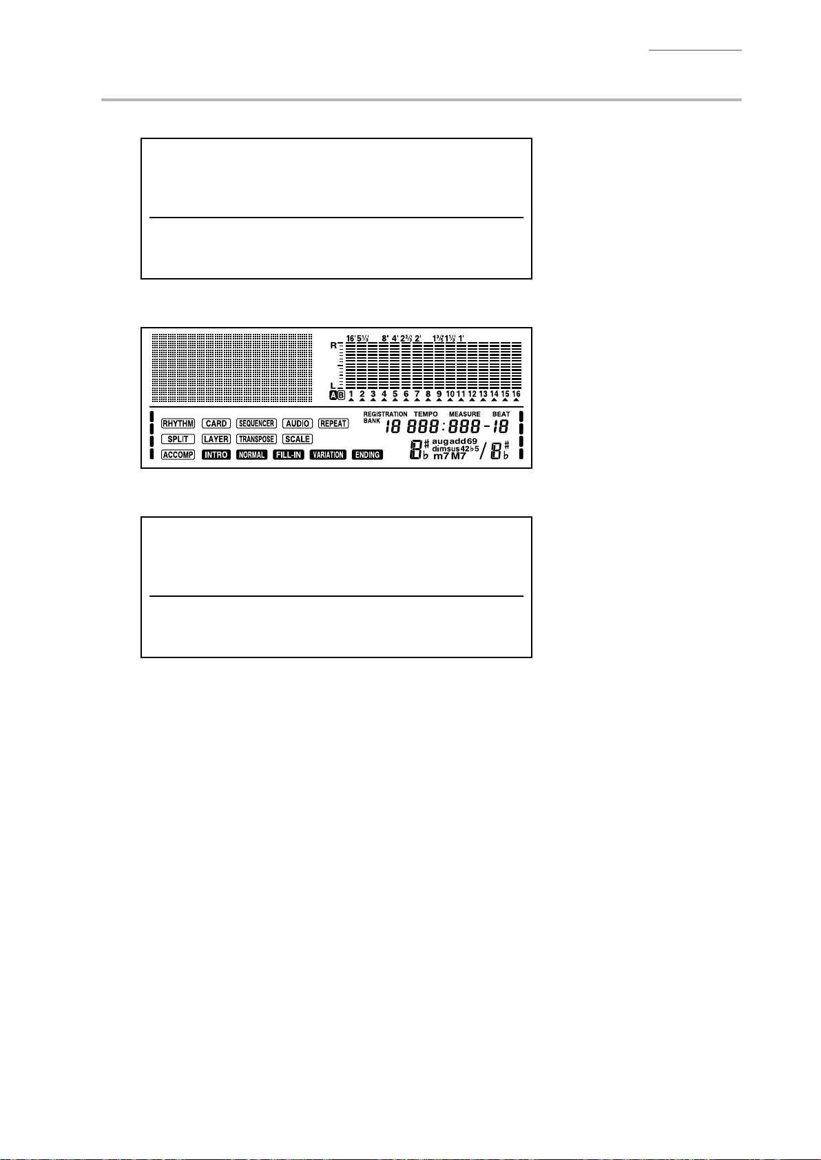
C-1. Press the “TONE [B]” button to select the “LCD CHECK”.
LCD TEST
C-2. Press the “TONE [B]” button and check to see if all LCDs are lit.
CTK-6300IN
C-3. Press the “TONE [B]” button and check to see if all LCDs are turned off.
C-4. Press the “RHYTHM [A]” button to return to the main screen.
– 34 –
Page 37

CTK-6300IN
D. ROM CHECK
D-1. Press the “TONE [E]” button to select the “ROM CHECK”.
ROM TEST
D-2. Press the “TONE [E]” button to perform the check.
NOTE: The display remains “ROM TEST” during the check.
NOTE: Whenthecheckiscomplete,theconrmationchordsoundsandthecheckresultappears.
ROM TEST
D-3. Check to see if the LCD is as shown below.
FLASH OK
D-4. Press the “RHYTHM [A]” button to return to the main screen.
– 35 –
Page 38

CTK-6300IN
E. RAM CHECK
E-1. Press the “TONE [F]” button to select the “RAM CHECK”.
RAM TEST
E-2. Press the “TONE [F]” button to perform the check.
NOTE: Whenthecheckiscomplete,theconrmationchordsoundsandthecheckresultappears.
RAM TEST...
E-3. Check to see if the LCD is as shown below.
RAM OK
E-4. Press the “RHYTHM [A]” button to return to the main screen.
F. ROM VERSION CHECK
F-1. Press the “TONE [I]” button to perform the “ROM VERSION CHECK”.
The ROM version appears on the LCD.
F-2. Check to see if the LCD is as shown below.
Release Ver.
F:0100
P:0000L
S:0100
F-3. Press the “RHYTHM [A]” button to return to the main screen.
– 36 –
Page 39

CTK-6300IN
G. SD CARD CHECK
G-1. Press the “TONE [G]” button to select the “SD CARD CHECK”.
SDCARD TEST
G-2. Press the “TONE [A]” button to perform the check.
NOTE: Whenthecheckiscomplete,theconrmationchordsoundsandthecheckresultappears.
SDCARD...
G-3. Check to see if the LCD is as shown below.
NOTE: If “OK” does not appear, try formatting the SD card and re-running the test. Please refer
to the user’s manual for how to format an SD card.
SDCARD OK
G-4. Press the “RHYTHM [A]” button to return to the main screen.
G-5. Remove the SD card.
– 37 –
Page 40

H. USB CHECK
H-1. Connect the main unit to the PC with a USB cable.
H-2. Press the “TONE [H]” button to select the “USB CHECK”.
ETC TEST
H-3. Press the “TONE [F]” button to perform the check.
H-4. Check to see if the LCD is as shown below.
USBCHK: OK
CTK-6300IN
H-5. Press the “RHYTHM [A]” button to return to the main screen.
H-6. Disconnect the USB cable.
I. AC ADAPTOR CHECK
I-1. Press the “TONE [K]” button to select the “AC ADAPTOR CHECK”.
I-2. Check to see if the LCD is as shown below.
PLUGGED
I-3. Press the “RHYTHM [A]” button to return to the main screen.
– 38 –
Page 41

EXPLODED VIEW
CTK-6300IN
12
10
23
8
SUB-PANEL-UNIT
BOTTOM VIEW
9
11
17
45~50 mm
38
18
22
21
20~25 mm
20
37
13
15
14
16
19
D8
D9
37
5
7
36
6
24
38
38
26
27
29
4
32
34
33
2
Refer to Bulletin EMI-415
35
25
28
30
31
1
KEYBOARD &
MAIN-CASE-UNIT
SIDE-PANEL-UNIT
75
76
39
74
74
75
77
78
81
77
– 39 –
79
78
82
80
82
83
Page 42

CTK-6300IN
LEFT-PANEL-UNIT
KEYBOARD & MAIN-CASE-UNIT
40
42
41
45
48
50
46 53
43
44
46
47
49
52
51
58
57
60
59
62
61
3
RIGHT-PANEL-UNIT
42
44
41
46
55
56
53
43
45
64
65
63
66
40
54
66
50
71
4653
69
68
67
71
72
71
73
– 40 –
70
Page 43

PARTS LIST
CTK-6300IN
CTK-6300IN
Notes:
1. Pricesandspecicationsaresubjecttochange
withoutpriornotice.
2. Refertothelatest“PartsPriceCode”at
“PARTSFINDER”ontheCasioServiceWEBsite
(https://www.servicecasio.com).
3. Asforsparepartsorderandsupply,referto
the“GUIDEBOOKforSparePartsSupply”,
publishedseparately.
4. Thenumbersinitemcolumncorrespondto
thesamenumbersindrawing.
– 41 –
Page 44

CTK-6300IN
CTK-6300IN_DI
N Item Code No. Parts Name Specification Q'ty R Remarks
MAIN PCB
N 1 10434449 PCBUNIT/MAIN TK-RJM512554*001 1 A MDA1
CN7 10236624 CONNECTOR/USB UBR24-4K5G00 1 C
CN12 10375067 CONNECTOR/SD SDK9BNSK13GNTBLFS4 1 B
D4,D5,
D11-D15
D8-D10 10346940 DIODE NNCD6.8RL-T1-AT 3 X
IC5 10211950 IC NJM2068M-D(TE1) 1 X
IC6 10398240 IC XC6402FV36PR-G 1 X
IC9 10256784 LSI/MEMORY CY62146EV30LL45ZST 1 C
IC11 10396648 LSI/MEMORY MX29GL128ELT2I-90G 1 C
IC12 10226394 IC TC74VHC08FT(EL.K) 1 X
IC13,IC14 10413602 IC TC7SH08FU(T5L.JF.T 2 X
L11 10193074 COIL DLW21HN181SQ2L 1 X
Q1,Q7,Q8 10399706 TRANSISTOR DSC500100L 3 X
Q2 10388215 TRANSISTOR 2SB1689T106 1 X
Q3 10402605 TRANSISTOR DSA500100L 1 X
X1 10375016 RESONATOR 7V48080006 1 X
2 10407990 PCBUNIT/POWER& TK-RJM511594*001 1 B
D1,D2 10273853 DIODE RSX301L-30TE25 2 X
D4 10210387 DIODE RSX101VA-30TR 1 X
D5,D6 10101686 DIODE UDZSTE-177.5B 2 X
D7 23901820 DIODE 1SS355TE-17 1 X
IC1 10306512 IC TDA7297 1 X
IC2 10375029 IC LA5756-MDB-E 1 X
IC3,IC5,IC6 10211950 IC NJM2068M-D(TE1) 3 X
IC8 10306415 IC BH3547F-E2 1 X
J2 10334294 JACK/DC KM02022ABMP 1 A
J3 10305218 JACK/PHONE JY-6316B*01-070 1 B
J4,J9 10206815 JACK/LINEOUTL,ASSIGNABLE JY-6314*01-030 2 B
J5 10206816 JACK/LINEOUTR JY-6314*01-130 1 B
J7 10305131 JACK/AUDIOIN ST-3529B 1 B
L1,L2,L4,
L6,L10,L11
L3,L8 10231919 COIL RB53-856396NP 2 X
L5 10232457 COIL RII7-860400NP 1 X
Q1 10400547 TRANSISTOR DSA500200L 1 X
Q2-Q5,Q8 10399706 TRANSISTOR DSC500100L 5 X
Q6,Q7 10407894 TRANSISTOR DSC250100L 2 X
VR2 10123103 VARIABLERESISTOR/forMainVolume RK09K12C0D1B 1BRefertoBulletinEMI-415
10009218 DIODE 1SS400TE61 7 X
POWER & AMP PCB
PSA1
RefertoBulletinEMI-415
10231920 COIL RB53-856397NP 6 X
KEYBOARD PCB
3 10401020 PCBUNIT/KEYBOARD/KYA TK-RJM508618*003 1 C KYA1/KYA2
D1-D61 10294400 DIODE LM1MA142WKT1G 61 X
CONSOLE PCB (LCA1, CNA1, CNA2, CNA3)
4 10407988 PCBUNIT/LCA1 TK-RJM511601*001 1 C LCA1
E1 10407911 ENCODER EVEGB1F1524M 1 B
IC1 10333225 LSI PD78F1153AGKSGAKAX 1 C
Q2 10400545 TRANSISTOR DMA501010R 1 X
Q12 10365234 TRANSISTOR DRC9114Y0L 1 X
Q20,Q21 10407895 TRANSISTOR DSC500200L 2 X
5 10407989 PCBUNIT/CNA1 TK-RJM511604*001 1 X CNA1
D7 10363781 LED 26-21/B1 1 X
D8,D9 10375069 LED SLR343WBD2PT3 2 X forLCDbacklight
D45 10336974 LED 26-21/R1 1 X
D46,D47 10101686 DIODE UDZSTE-177.5B 2 X
6 10423944 PCB/CNA2 RJM511047-002V02 1 X CNA2
7 10423945 PCB/CNA3 RJM511047-003V02 1 X CNA3
– 42 –
Page 45

CTK-6300IN
CTK-6300IN_DI
N Item Code No. Parts Name Specification Q'ty R Remarks
PANEL UNIT
8 10407929 KNOB/forDIAL RJM511443-001V01 1 C
9 10407931 DISPLAYPLATE RJM511445-001V01 1 X
10 10193270 KNOB/forROTARY RJM502503-008V02 1 C
N 11 10434266 CASE/PANEL RJM511425-012V01 1 X
12 10407932 BRACKET/V-ZERO RJM511447-001V01 1 X
13 10412041 TOPPIECEB RJM511753-001V01 1 X
14 10407920 RUBBERBUTTON/A RJM511432-001V01 1 X
15 10419561 RUBBERBUTTON/B RJM511433-001V02 1 X
16 10422034 RUBBERBUTTON/C RJM511434-001V02 1 X
17 10407923 RUBBERBUTTON/D RJM511435-001V01 1 X
18 10422037 RUBBERBUTTON/E RJM511436-001V02 1 X
19 10407925 RUBBERBUTTON/F RJM511437-001V01 1 X
20 10407926 RUBBERBUTTON/G RJM511438-001V01 1 X
21 10407927 RUBBERBUTTON/J RJM511439-001V01 1 X
22 10419564 RUBBERBUTTON/L RJM511441-001V02 1 X
23 10411881 LCD ZAS-SR012922DN01 1 X
24 10203058 RUBBERCONNECTOR/forLCD RJM505822-001V01 2 X
25 10407930 BEZEL/forDIAL RJM511444-001V01 1 X
26 10270485 SPONGE/8X75 M441167-001V01 2 X
27 10407941 TOPPIECE RJM511589-001V01 1 X
28 10250780 FILM RJM507061-001V01 1 X
29 10248119 BACKLIGHTPLATE RJM506818-001V01 1 X
30 10380402 REFLECTOR RJM502577-001V03 1 X
31 10407942 SPONGE/17X45 RJM511610-001V01 1 X
32 10423542 DOUBLEFACEDTAPE/6X10 RJM506386-002V01 1 X
33 10445070 SHAFT/forROTARYKNOB RJM511468-002V01 1XRefertoBulletinEMI-415
34 10424518 PACKING RJM512070-001V01 1 X
35 10407942 SPONGE/17X45 RJM511610-001V01 1 X
SUB PANEL UNIT
36 10407918 PANEL/SUB RJM511428-001V01 1 X
37 10215082 FABRICTAPE/5X200 RJM506371-001V01 1 X
38 10053728 FABRICTAPE/10X42 M440240-2 4 X
39 10407992 BENDERUNIT TK-RJM511118*003 1 C
SIDE PANEL UNIT
40 10375063 SPEAKERCOVER/forFULLRAGE RJM510710*001V01 2 X
41 10412019 SPEAKERCOVER/forPORT RJM510711*003 2 X
42 10375066 SPEAKERCOVER/forTWEETER RJM510713*001V01 2 X
43 10408934 SPONGE/30X35 M441046-001V01 2 X
44 10309765 BUZZER HM-2720MYLAR 2 X Tweeter
45 10407934 DOUBLEFACEDTAPE/D24 RJM511582-001V01 2 X
46 10179176 PACKING/20X20 RJM505231-001V01 4 X
47 10263730 RUBBERFOOT M441160-001V01 1 X
48 10407916 CASE/SIDEPANEL/LEFT RJM511426-001V01 1 X
49 69276140 FABRICTAPE/10X10 M440855-1 2 X
50 10375017 SPEAKER C12J09 2 X
51 10417028 WIRE 1007TASC24400W8030 1 X White
52 10417029 WIRE 1007TASC24400G8030 1 X Green
53 10281936 SPONGE/35X80 M440930-001V01 3 X
54 10416386 CASE/SIDEPANEL/RIGHT RJM511427-001V02 1 X
55 10417030 WIRE 1007TASC24600B8030 1 X Blue
56 10417031 WIRE 1007TASC24600T8030 1 X Brown
– 43 –
Page 46

CTK-6300IN
CTK-6300IN_DI
N Item Code No. Parts Name Specification Q'ty R Remarks
KEYBOARD & MAIN CASE UNIT
57 10399802 WHITEKEY/CB RJM507243*004V03 4 A
58 10399803 WHITEKEY/CS RJM507244*004V03 1 B
59 10406652 BLACKKEY/10p RJM506595-005V03 2 A
60 10406653 BLACKKEY/5p RJM506595-006V03 1 B
61 10269451 RUBBERCONTACT/CB RJM507656-001V01 4 A
62 10270393 RUBBERCONTACT/CS RJM507657-001V01 1 B
63 10407987 CASEUNIT/MAIN TK-RJM511577*001 1 X
64 10373683 FELT/LOWERLIMIT/KEYBOARD RJM508593-001V02 1 X
65 10317116 FELT/DAMPER/KEYBOARD RJM509138-001V01 1 X
66 10284332 BRACKET/forSTAND M440866-001V02 2 X
67 10263726 BATTERYTERMINAL/+ M441101-001V02 1 X
68 10263727 BATTERYTERMINAL/- M441102-001V02 1 X
69 10419558 BATTERYTERMINAL/A M441099-001V03 2 X
70 10419559 BATTERYTERMINAL/B M441100-001V03 3 X
71 69226920 RUBBERFOOT M41361-6 4 X
72 10373681 FELT/UPPERLIMIT/KEYBOARD M440342-001V03 1 X
73 10271778 BATTERYCOVER TK-M341288*002 1 X
74 10221193 SPONGE/40X200 RJM506471-001V01 2 X
75 10321174 PACKING M440856-001V02 4 X
76 10417027 PACKING/22X480 M440448-001V01 1 X
77 10214396 PACKING/7X180 RJM506032-001V01 2 X
78 10337918 FABRICTAPE/5X30 M440583-003V01 2 X
79 10381069 LOWERCOVER/A RJM508655-001V04 1 X
80 10381070 LOWERCOVER/B RJM508656-001V04 1 X
81 10381071 LOWERCOVER/C RJM508657-001V04 1 X
82 10419560 RUBBERFOOT M441160-002V01 2 X
N 83 10434262 LABEL/RATING RJM504373-092V01 1 X
ACCESSORIES
- 10421868 MUSICSTAND M141071-001V01 1 C
- 10430927 ACADAPTOR AD-A12150LW-F3B 1 B withoutACCORD
- 10361067 ACCORD EC2LT-M002A 1 X forACADAPTOR
– 44 –
Page 47

Main PCB: M842-MDA1
(to PSA1/PAD (Y))
(to LCA1/CN1)
(to LCA1/CN1)
Not used
SCHEMATIC DIAGRAMS
USB (CN7)
CTK-6300IN
SD
SD
(CN12)
(CN12)
(to PSA1/
CN15)
(to LCA1/CN9) (to KYA1/CN801) (to KYA2/CN804)
– 45 –
Page 48

Power & Amp PCB: M842-PSA1
CTK-6300IN
LEFT SPEAKER
LEFT BUZZER
Not used
(to LEFT SPEAKER)
DC 12 V (J2)
PHONES (J3) AUDIO IN (J7)
LINE OUT (L/MONO)
(J4)
LINE OUT (R)
(J5)
(to MDA1/
CN15)
SUSTAIN/ASSIGNABLE
(J9)
RIGHT SPEAKER
RIGHT BUZZER
PITCH BEND
(to MDA1/
CN1)
(to BATTERY)
MAIN VOL.
(VR2)
(to RIGHT SPEAKER)
(to PITCH BEND)
– 46 –
Page 49

Console PCB: M842-LCA1 (1/2)
Not used
CTK-6300IN
(to CNA1/
CN2)
(to MDA1/
CN13, CN14)
(to MDA1/
CN10)
DIAL
(to CNA1/
CN7)
(to CNA1/
CN5)
– 47 –
Page 50

Console PCB: M842-LCA1 (2/2)
CTK-6300IN
Not used
– 48 –
Page 51

Console PCB: M842-CNA1
POWER
SWITCH
CTK-6300IN
Not used
(to LCA1/CN3)
(to LCA1/CN7)
(to LCA1/CN5)
– 49 –
Page 52

Keyboard PCB: M802-KYA1
(to MDA1/CN2) (to KYA2/CN803)
CTK-6300IN
– 50 –
Page 53
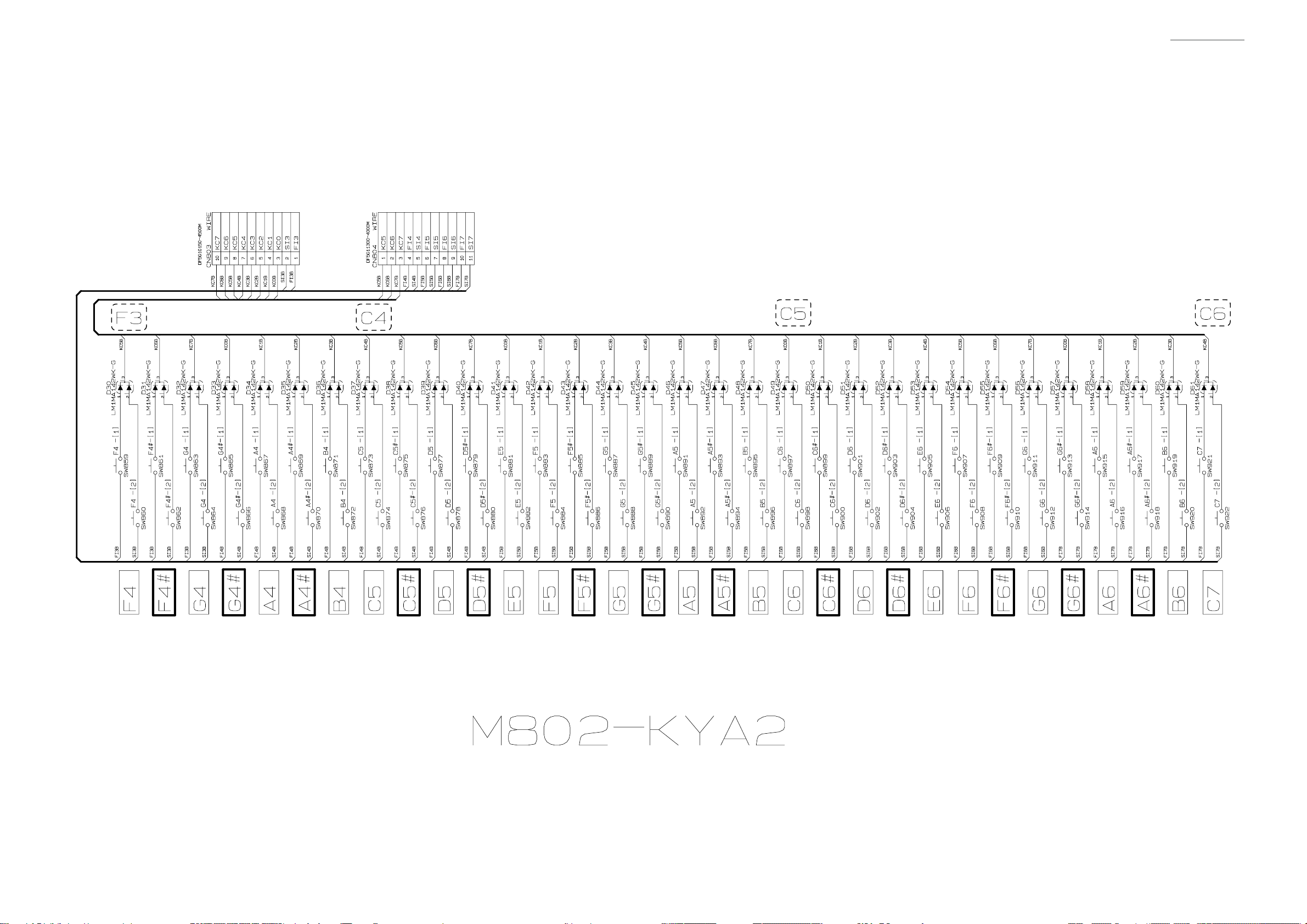
Keyboard PCB: M802-KYA2
(to KYA1/CN802) (to MDA1/CN3)
CTK-6300IN
– 51 –
Page 54

Ver. 1 : Jul. 2012
• Correction of the DIAGNOSTIC PROGRAM (P31 and P36)
Ver. 2 : Feb. 2013
• Correction of the EXPLODED VIEW (P39)
• Correction of the PARTS LIST (P42 and P43)
CASIO COMPUTER CO., LTD.
CS Technical Department
TOKYO, JAPAN
 Loading...