

Page 1
(with price)
CTK-630
CONTENTS
Page
Specifications ................................................................................................................................... 2
Block Diagram.................................................................................................................................. 3
Circuit Description ............................................................................................................................ 4
Troubleshooting ............................................................................................................................. 10
Major Waveforms ........................................................................................................................... 11
Printed Circuit Boards .................................................................................................................... 12
Schematic Diagrams ...................................................................................................................... 13
Exploded View ............................................................................................................................... 16
Parts List ........................................................................................................................................ 17
ELECTRONIC KEYBOARD
Page 2

SPECIFICATIONS
GENERAL
Number of keys: 61
Polyphonic: 24-note
Preset tones: 100, Tone expander: Layer On/Off, Split On/Off
Keyboard controls: Touch response: On/Off, Key transpose: Range from F# to F by
a semitone increment, Pitch bend: 12 steps up and down (a seminote at
muximum)
Auto-rhythms: 100, Tempo control: 40 to 255
Auto-accompaniment: Mode: CASIO Chord/Fingered/Full-Range Chord 1/
Full-Range Chord 2
Controller: Intro/Fill-In, Synchro/Ending, Normal/Variation
Easy presets: 50, including — Free Session (Chord): 30, Free Session (Song): 10,
Melody Composition: 10
Reverb effects: Hall/Stage/Room
Musical pads: 8
Pad variations: 50, including — Pops: 10, Rock: 10, Jazz/Fusion: 10, Dance/Funk: 10
European: 2, Latin/Various: 5, Drums/Percussion: 5
Song memory: 3, Real-time recording, Memory capacity: Approx. 1200 notes in total
Demo tunes: 3, including — A Night has 9000 Bars (arranged and programmed by
Thomas Hirsch), Wanting This (Edward Alstrom), Supersonic Remorse
(Edward Alstrom)
Demo tune program: Repeat/Skip
Tuning control: 440Hz ± 50 cents
Built-in speakers: 12 cm dia. 2 W input rating: 2 pcs.
MIDI: 16 multi-channel reception
Terminals: Phone Jack [Output impedance: 90 Ω, Output voltage: 4.6 V(rms)
MAX], Sustain Jack, MIDI Jacks (IN, OUT), AC Adapter Jack (9 V)
Auto power off: Approximately 6 minutes after the last operation
Power source: 2-way AC or DC source
AC: AC adapter
DC: 6 D size dry batteries
Power consumption: 7.7 W
Dimensions (HWD): 104 x 931 x 353 mm (4-1/16 x 36-5/8 x 13-7/8 inches)
Weight: 4.7 kg (10.4 lbs) including batteries
ELECTRICAL Nominal Limit
Current drain with 9 V DC:
No sound output 220 mA 220 mA ± 30 %
Maximum volume 900 mA 900 mA ± 30 %
with white keys C4 to G5 pressed in Recorder tone
Volume: maximum, Touch response: maximum
Layer: On, Reberv: Off
Phone output level (Vrms with 8 Ω load each channel):
with key C4 pressed in Recorder tone 125 mV 125 mV ± 30 %
Sound pressure (at 10 cm away from speaker):
with key A3 pressed in Recorder tone 98 dB 98 dB ± 10 dB
Minimum operating voltage: 5.8 V 6.0 V
— 2 —
Page 3
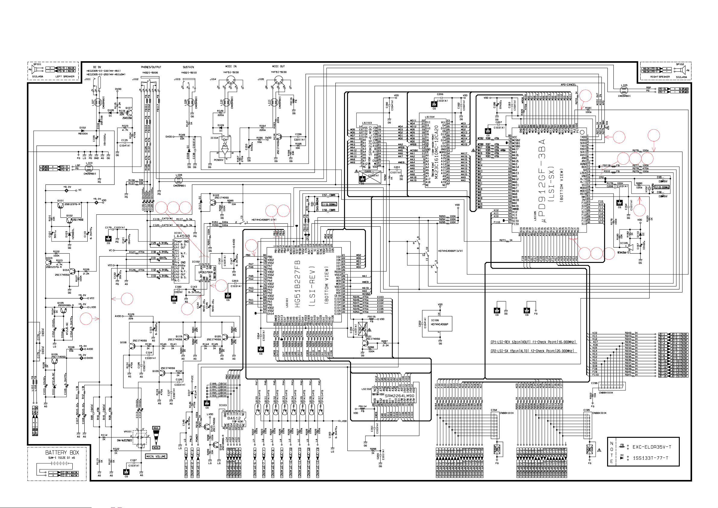
BLOCK DIAGRAM
Working Storage
RAM (64K-bit)
LSI103
SRM2264LM90
MIDI
Power Switch
VDD
Buttons
INOUT
Reset IC
IC105
RE5VA35AA
Sound Source ROM
(16M-bit)
LSI104
MX23C1610MC-
12CA20
Effect RAM
(64K-bit)
LSI102
SRM2264LM90
RESET
MA0 ~ MA19
MA0, MA1
EA0 ~
EA12
EIO0 ~
EIO7
MA0
~
MA12
MD0 ~ MD15
MD0
~
MD7
LSI101
HG51B227FB
LRCK SO BCK
DSP
KI0 ~ KI2
CPU
LSI105
UPD912GF-3BA
BCK, SO, LRCK
PA0 ~ PA7
PB0 ~ PB4
FI0 ~ FI10
SI0 ~ SI19
KC0 ~ KC7
LED driver
Q110 ~ Q117
LED driver
IC103
BA612
FI8 ~ FI10, SI8
Keyboard
La ~ Lg, Lp
LEDs /
7Seg. LED
LC0 ~ LC4
Speakers
Output
D/A Converter
IC102
UPD6379GR
Filter
Q108, Q109
Q119, Q120
Main
Volume
Power Amplifier
IC101
LA4598
— 3 —
APO
LVDD
VCC
AVDD
Power Supply Circuit
Q101 ~ Q106
D101, D103, D104
DVDD
VC
VDD
Page 4
CIRCUIT DESCRIPTION
KEY MATRIX
KC0 KC1 KC2 KC3 KC4 KC5 KC6 KC7
FI0 C2 (1) C#2 (1) D2 (1) D#2 (1) E2 (1) F2 (1) F#2 (1) G2 (1)
SI0 C2 (2) C#2 (2) D2 (2) D#2 (2) E2 (2) F2 (2) F#2 (2) G2 (2)
FI1 G#2 (1) A2 (1) A#2 (1) B2 (1) C3 (1) C#3 (1) D3 (1) D#3 (1)
SI1 G#2 (2) A2 (2) A#2 (2) B2 (2) C3 (2) C#3 (2) D3 (2) D#3 (2)
FI2 E3 (1) F3 (1) F#3 (1) G3 (1) G#3 (1) A3 (1) A#3 (1) B3 (1)
SI2 E3 (2) F3 (2) F#3 (2) G3 (2) G#3 (2) A3 (2) A#3 (2) B3 (2)
FI3 C4 (1) C#4 (1) D4 (1) D#4 (1) E4 (1) F4 (1) F#4 (1) G4 (1)
SI3 C4 (2) C#4 (2) D4 (2) D#4 (2) E4 (2) F4 (2) F#4 (2) G4 (2)
FI4 G#4 (1) A4 (1) A#4 (1) B4 (1) C5 (1) C#5 (1) D5 (1) D#5 (1)
SI4 G#4 (2) A4 (2) A#4 (2) B4 (2) C5 (2) C#5 (2) D5 (2) D#5 (2)
FI5 E5 (1) F5 (1) F#5 (1) G5 (1) G#5 (1) A5 (1) A#5 (1) B5 (1)
SI5 E5 (2) F5 (2) F#5 (2) G5 (2) G#5 (2) A5 (2) A#5 (2) B5 (2)
FI6 C6 (1) C#6 (1) D6 (1) D#6 (1) E6 (1) F6 (1) F#6 (1) G6 (1)
SI6 C6 (2) C#6 (2) D6 (2) D#6 (2) E6 (2) F6 (2) F#6 (2) G6 (2)
FI7 G#6 (1) A6 (1) A#6 (1) B6 (1) C7 (1)
SI7 G#6 (2) A6 (2) A#6 (2) B6 (2) C7 (2)
FI8 Pad A (1) Pad B (1) Pad C (1) Pad D (1) Pad E (1) Pad F (1) Pad G (1) Pad H (1)
SI8 Pad A (2) Pad B (2) Pad C (2) Pad D (2) Pad E (2) Pad F (2) Pad G (2) Pad H (2)
FI9
FI10
Intro/
Fill-In
Bend
Up
Synchro/
Ending
Bend
Down
Start/
Stop
Normal/
Variation
Tempo
Up
Tempo
Down
Accomp.
Volume
Up
Accomp.
Volume
Down
KI0 Mode Reverb 0 1 4 7 Layer Split
KI1 Rhythm Tone – 2 5 8
KI2
Easy
Preset
Pad + 3 6 9 Memory
Transpose
Tune/MIDI
Demo
Touch
Response
— 4 —
Page 5
Note: Each key has two contacts,
the first conatct (1) and second contact (2).
NOMENCLATURE OF KEYS
Second contact (2)
Key
First contact (1)
FI
KC
SI
C#2
C2 D2E2F2G2A2 B2 C3 D3
F#2D#2
C#3A#2G#2
F#3 G#3
D#3
E3
F3 G3 A3 B3 C4 D4 E4 F4 G4 A4 B4 C5 D5 E5 F5 G5 A5 B5
A#3 C#4 D#4
F#4 G#4
A#4
C#5
D#5
F#5 G#5
A#5
C#6
C6
G#6F#6D#6
A#6
POWER SUPPLY CIRCUIT
The power supply circuit generates six voltages as shown in the following table. VDD voltage is always
generated. The others are controlled by APO signal from the CPU.
Name Voltage For operation of
VDD +5 V CPU, Reset IC, DSP, Sound source ROM, Working storage RAM, Effect RAM
DVDD +5 V Power jack, Sustain jack, MIDI jack
AVDD +5V DAC, Filter
LVDD +4.5 V LED Driver
VCC +9 V Power amplifier, Pilot lamp
VC +9 V Power amplifier
B6A6G6F6E6D6
C7
RESET CIRCUIT
When batteries are set or an AC adapter is connected, the reset IC provides a low pulse to the CPU. The
CPU then initializes its internal circuit, and clears the working storage RAM.
When the power switch is pressed, the CPU receives a low pulse of POWER signal. The CPU sends
APO signal to supply ground source for the DSP, also sends a reset signal to the DSP.
Battery set
VDD
Reset IC
IC105
RE5VA35AA
POWER
From power switch
RESET
VDD
CPU
LSI105
UPD912GF-3BA
SCKO
NMI
— 5 —
Reset signal
PLE
HG51B227FB
APO
VDD
DSP
LSI101
Page 6
CPU (LSI105: UPD912GF-3BA)
The 16-bit CPU contains a 1k-byte RAM, three 8-bit I/O ports, two timers, a keycontroller and serial interfaces.
The CPU detects key velocity by counting the time between first-key input signal FI and second-key SI from
the keyboard. The CPU reads sound data and velocity data from the sound source ROM in accordance with
the selected tone; the CPU can read rhythm data simultaneously when a rhythm pattern is selected. Then the
CPU provides 16-bit serial sound data to the DSP. The CPU also controls MIDI input/output and stores
sequencer data into the working storage RAM.
The following table shows the pin functions of LSI105.
Pin No. Terminal In/Out Function
1 TXD0 Out MIDI signal input
2 RXD0 In MIDI signal output
3 SCK0 Out APO (Auto Power Off) signal output
4, 5 TXD1, RXD2 — Not used. Connected to ground.
6 SCK1 Out 1 MHZ synchronizing pulse output
7 AVCC In Ground (0 V) source
8, 9 AN0, AN1 — Not used. Connected to ground.
10 AGND In Ground (0 V) source
11 BCK Out Bit clock output
12 SO Out Serial sound data output
13 LRCK Out Word clock output
14 GND In Ground (0 V) source
15, 16 XLT0, XLT1 In/Out 20 MHz clock input/output
17 VCC In +5 V source
18, 19 MD0, MD1 In Mode selection terminal
20 RSTB In Reset signal input
21 NMI In Power ON signal input
22 INT — Not used. Connected to ground.
23 ~ 30
31 ~ 38 KC0 ~ KC7 Out Terminal for key scan signal
FI0 ~ FI3
SI0 ~ SI3
In Terminal for key input signal
39 ~ 46
47, 48 FI8, SI8 In Terminal for pad input signal
49 FI9 In Terminal for button input signal
50 SI9 In Sustain signal input
51 FI10 In Terminal for button input signal
52 SI10 In Not used
53 ~ 55 KI0 ~ KI2 In Terminal for button input signal
56 MWNB Out Write enable signal output
57 ~ 76 MA0 ~ MA17 Out Address bus
77 MCSB0 Out Chip enable signal output for the sound source ROM
78 MCSB1 Out Not used
79 MCSB2 Out Chip enable signal output for the DSP
FI4 ~ FI7
SI4 ~ SI7
In Terminal for key input signal
— 6 —
Page 7

Pin No. Terminal In/Out Function
80 VCC In +5 V source
81 GND In Ground (0 V) source
82 MRDB Out Read enable signal output for the sound source ROM
83 ~ 98 MD0 ~ MD15 In/Out Data bus
99 PLE Out Reset signal output for the DSP
100 P17 In APO cancellation signal input
DIGITAL SIGNAL PROCESSOR (LSI101: HG51B227FB)
The DSP receives 16-bit serial sound data output from the CPU and adds the selected effect to the sound
data using the effect RAM. Then the DSP provides the sound data to the DAC. The DSP contains two I/O
ports, which controls LEDs.
The following table shows the pin functions of LSI101.
Pin No. Terminal In/Out Function
1 ~ 4, 80 PB0 ~ PB4 Out LED drive signal output
5 SO Out Serial sound data output for the DAC
6 WCKO Out Word clock output for the DAC
7 VDD3 In +5 V source
8 TEST — Not used.
9 RESB In Reset signal input
10 VSS2 In Ground (0 V) source
11, 12 XIN, XOUT In/Out 16 MHz clock input/output
13 WCKI In Word clock input from the CPU
14 SI In Serial sound data input from the CPU
15 BCKI In Bit clock input from the CPU
16 SINC In 1 MHz synchronizing pulse input
17 VDD2 In +5 V source
18 ~ 25 IO0 ~IO7 In/Out Data bus
26 RCEB Out Chip enable signal output for the working storage RAM
27 VSS3 In Ground (0 V) source
28 AD1 In Address bus
29 OEB In Not used. Connected to +5 V source.
30 WEB In Write enable signal input
31 VDD3 In +5 V source
32 CE2 In Chip enable signal input. High active.
33 AD0 In Address bus
34 CE1B In Chip enable signal input. Low active.
35 ~ 41, 43 EIO0 ~EIO7 In/Out Data bus for the effect RAM
42 , 44, 46 ~ 48,
51 ~57, 59
45 ECEB Out Chip enable signal output for the effect RAM
49 EOEB Out Read enable signal output for the effect RAM
EA0 ~ EA12 Out Address bus for the effect RAM
— 7 —
Page 8
Pin No. Terminal In/Out Function
50 VSS3 In Ground (0 V) source
58 EA13 Out Not used
60 EWEB Out Write enable signal output for the effect RAM
61 EA14 Out Not used
62, 66, 70, 74, 78 VSS2 In Ground source
63, 67, 71, 75, 79 VDD2 In +5 V source
64, 65, 68, 69,
72, 73, 76, 77
PA0 ~ PA7 Out LED segment signal output
DAC (IC102: UPD6379GR)
The DAC receives 16-bit serial data output from the DSP. The data contains digital sound data of the
melody, chord, bass, and percussion for the right and left channels. The DAC converts the data into
analog waveforms and output them to each channel separately.
Synch signal
L OUT
R OUT
DAC
IC102
UPD6379GR
SI
LRCK
CLK
Data
Word clock
WCKO
Bit clock
SO
DSP
LSI101
HG51B227FB
SINC
SI
Word clock
WCKI
Bit clock
BCKI
Data
SCK1
SO
LRCK
BCK
CPU
LSI105
UPD912GF-3BA
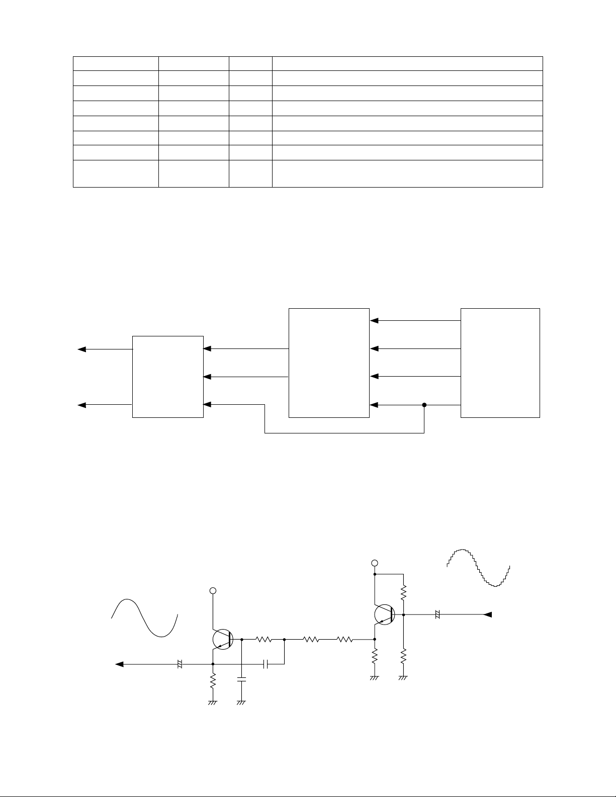
FILTER BLOCK
Since the sound signals from the DAC are stepped waveforms, the filter block is added to smooth the
waveforms.
AVDD
AVDD
To main volume
10V22µ
2SC1740SQ
470
AG
1K
C332(H)
AG
C333(H)
2SC1740SQ
1K 1K
— 8 —
1K
AG
22K
50V0.22µ
47K
AG
From the DAC
Page 9
POWER AMPLIFIER (IC101: LA4598)
The power amplifier is a two-channel amplifier with standby switch.
The following table shows the pin function of IC101.
Pin No. Terminal In/Out Function
1 Power GND In Ground (0V) source
2 Ch1 B.S. — Terminal for a bootstrap capacitor
3 Ch1 OUT Out Channel 1 output
4 VCC In +9V source
5 Ch1 N.F. In Negative feedback input
6 Ch1 IN In Channel 1 input
7 D.C. — Terminal for a decoupling capacitor
8 Pre GND In Ground (0V) source
9 Stand by In Power control signal input. 0 V: Off, +9 V: On
10 Ch2 IN In Channel 2 input
11 Ch2 N.F. In Negative feedback input
12 Ch2 OUT Out Channel 2 output
13 Ch2 B.S. — Terminal for a bootstrap capacitor
14 NC — Not used
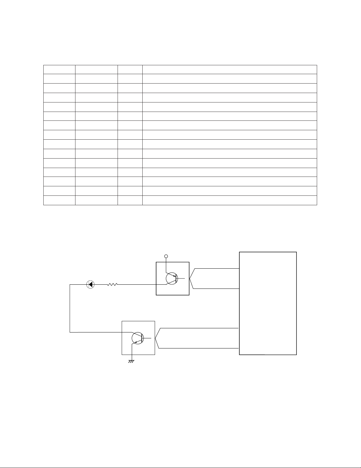
LED DRIVING
LC0 ~LC4
IC103
BA612
LED Driver
La ~ Lg, Lp
LG
LVDD
Q110 ~ Q117
LED Driver
PB0 ~ PB4
PA0 ~ PA7
DSP
LSI101
HG51B227FB
— 9 —
Page 10
TROUBLESHOOTING
Nature of Trouble Faulty Block Cause/Remedy
No power Power supply circuit Faulty Q101 ~ Q106.
Replace Q101 ~ Q105.
Faulty D101 ~ D105.
Replace D101 ~ D105.
Power jack (J101) Open J101 or poor soldering.
Replace J101 or resolder.
Reset IC (IC105) Faulty IC105. Replace IC105.
CPU (LSI105) Faulty LSI105. Replace LSI105.
Oscillator (X102) Open X102. Replace X102.
No sound at all Power amp (IC101) Open or shorted IC101. Replace IC101.
CPU (LSI105) Faulty LSI105. Replace LSI105.
Sound source ROM (LSI104) Faulty LSI104. Replace LSI104.
DSP (LSI101) Faulty LSI101. Replace LSI101.
Oscillator (X101) Open X101. Replace X101.
DAC (IC102) Faulty IC102. Replace IC102.
Working storage RAM
(LSI103)
Distorted sound Sound source ROM (LSI104) Faulty LSI104. Replace LSI104.
DSP (LSI101) Faulty LSI101. Replace LSI101.
Faulty LSI103. Replace LSI103.
Certain keys do not
function
Certain buttons do
not function
A certain button or
key does not function
Effect RAM (LSI102) Faulty LSI102. Replace LSI102.
Power amp (IC101) Open or shorted IC101. Replace IC101.
Key matrix Open circuit on KC, FI or SI line.
Replace keyboard PCB assembly.
Button matrix Open circuit on KC, FI, SI or KI line.
Replace console PCB assembly.
Key or button matrix Dust on the contact. Clean the contact.
— 10 —
Page 11
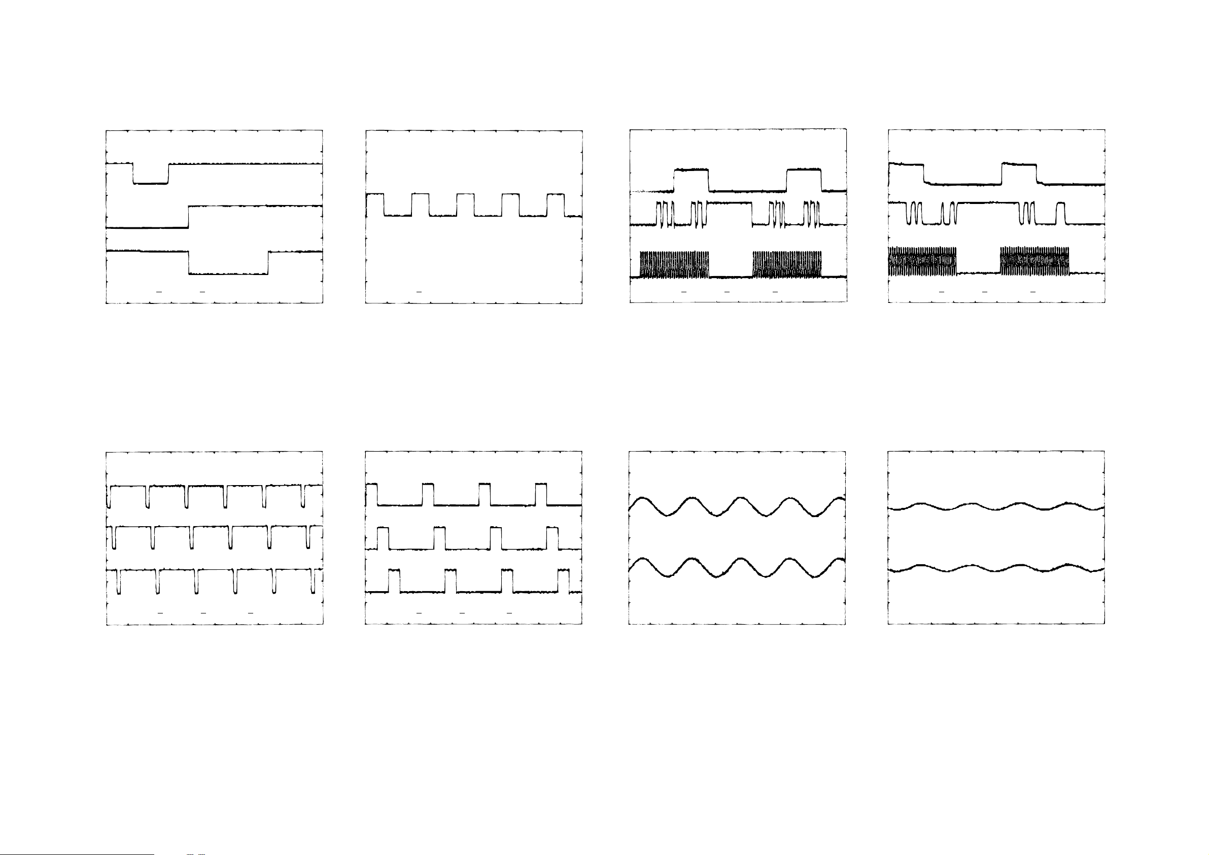
MAJOR WAVEFORMS
1
2
3
CH1: CH2:
5 V5 V
1 POWER ON signal
UPD912GF-3BA pin 21
2 APO signal
UPD912GF-3BA pin 3
3 Reset signal for the DSP
UPD912G-3BA pin 99
0.1 s
CH1
CH2
4
5 VCH1:
4 Synchronizing pulse
UPD912GF-3BA pin 6
20 µs
CH1
A
B
C
5 VCH1: 5 VCH2: 5 VCH3:
A Word clock LRCK
UPD912GF-3BA pin 13
B Data signal SO
UPD912GF-3BA pin 12
C Bit clock BCK
UPD912GF-3BA pin 11
2 µs
D
CH1
E
CH2
F
CH3
Note: On
2 µs
CH1
CH2
CH3
5 VCH1: 5 VCH2: 5 VCH3:
D Word clock LRCK
UPD6379GR pin 1
E Data signal SI
UPD6379GR pin 2
F Bit clock CLK
UPD6379GR pin 3
5
6
7
5 VCH1: 5 VCH2: 5 VCH3:
5 Key scan signal KC0
UPD912GF-3BA pin 31
6 Key scan signal KC1
UPD912GF-3BA pin 32
7 Key scan signal KC2
UPD912GF-3BA pin 33
50 µs
CH1
CH2
CH3
8
9
0
5 VCH1: 5 VCH2: 5 VCH3:
8 LED drive signal PB0
HG51B227FB pin 80
9 LED drive signal PB1
HG51B227B pin 1
0 LED drive signal PB2
HG51B227FB pin 2
5 ms
CH1
CH2
CH3
G
H
CH1: . 1 V
~
CH2: . 1 V
G DAC output (R-ch)
UPD6379GR pin 5
H DAC output (L-ch)
UPD6379GR pin 8
1 ms
CH1
I
CH2
J
~
CH1: . 1 V~CH2: . 1 V
1 ms
CH1
CH2
~
I Amp. input (R-ch)
LA4598 pin 6
J Amp. input (L-ch)
LA4598 pin 10
Tone : Whistle (70)
Key : A4
Touch response : Off
Reverb : Off
Volume : Maximum
— 11 —
Page 12

Main PCB JCM461-MA1M
PRINTED CIRCUIT BOARDS
18172019 1416 1015 89 12765 34 112 113
A
B
C
PS
VC
Q103
D102
W
R
C177
C101
E
C175
BK R
D106
B
R101
R102
L102
PZ
L107
B
R103
Q104
L103
Q101
L101
D103
B
E
B
R106
1
100
E
E
Q102
75
C103
C176
J101
R107
B
C178
VCC
C110
Q106
D101
C187
R104
100
D105
C109
125
175
150
D104
C102
Q105
EB
C104
R105
E
.
3
3
.
.
21
21
C105
300
VR101
J102
FB101
FB102
5
C116
L VDD
275
75
D107
R146
FB103
FB104
100
125
250
C114
C179
C113
C146
C123
5
2
100
R125
R129
75
1
R126
125
5
C117
DVDD
75
E
B
E
B
R136
Q108
Q109
FB117
R134
R135
R108
75
AVDD
R131
R133
R114
R122
C124
C126
5
C122
C127
R137
C125
5
C128
C121
R130
R132
JC
75
C107
R140
R144
J103
C118
C129
C135
C136
C120
R141
R145
5
R283
R286
C130
R111
C106
E
100
E
R110
Q119
R281
Q120
R284
L109
R118
R109
16
5
C137
R117
R127
B
B
C119
100
R113
J104
C131
R121
R282
R285
VDD
C144
C145
125
C108
3
C133
IC101
R128
R112
C112
L110
R147
R120
R119
IC102
C180
R148
C132
C147
R149
D108
150
R298
Q123
5
C138
175
C184
E
D109
L108
D111
R150
C143
1
FB116
IC104
B
C142
R116
R115
Q124
R299
R297
B
FB119
Q122
B
FB123
J105
Q118
R163
L111
R164
C153
R156
R157
B
Q107
C192
E
C193
E
E
Q110EQ
B
C183
R222
JA
B
R166
E
R165
FB124
5
R123
E
C115
C191
B
R223
R291
R151
111
R224
R124
E
B
R225
R290
100
R289
C190
100
C189
R287
Q121
IC103
Q112EQ113EQ114EQ115EQ116EQ117
B
B
R226
R227
R228
R229
16
4
C156
125
E
B
R216
IC106
R293
LSI101
R260
R294
R259
R258
R295
R257
5
100
R256
1
R255
R254
R192
R253
R193
R252
R194
X101
R172
FB110
FB111
C158
B
R186
FB115
C203
R187
C204
C161
R188
C157
C159
R189
R269
R190
75
100
R268
R191
C194
R300
R266
R265
C200
R264
5
R263
250
R262
R261
LSI102
R296
5
C182
125
R288
B
B
FB114
R184
R185
395
R251
R195
R250
R196
C205
R249
R197
C202
75
LSI103
R248
R247
R198
R199
JB
75
C201
R246
175
R245
R200
FB120
250
R201
6
R202
C160
R292
R203
R204
R205
17
200
R206
R279
R207
R208
R278
LSI104
R209
R277
R210
R276
R211
C206
R212
FB121
R304
R213
R214
C162
75
250
R307
R215
C195
R308
C186
R309
R303
R301
FB122
C163
5
C207
150
R306
R305
200
125
R181
R271
R272
175
C199
R273
R274
LSI105
C198
R275
225
C208
R310
FB118
C173
C165
R280
75
C166
R178
R179
C174
C164
R183
R180
R302
L105
X102
R182
C196
D110
R242
R243
R244
R237
R236
R235
R234
R233
R232
R231
R230
R238
R239
R240
R241
3
1
IC105
BL
PR
Y
1
JD
15
78
C167
245
Console PCB JCM461-CN1M
D451
D450
D449
D448
D447
D446
D445
D444
D443
D442
D441
D440
D439
D438
D437
D436
Top View
NO.
JC
1
LED403
LED404
LED405
LED406
D402
D404
D405
LED407
LED408
5
D403
LED409
LED402
JD
1
LED415
15 JD 1
15
LED416
5
LED413
LED414
D431
D434
D435
D432
D429
D425
D430
D433
55
D421
5
D422
D418
D426
D423
D420 D419
D424
5
55
5
5
D427
5
5
D428
5
5
5
D417 D416 D415 D414
LED401
5
LED412
5
5
LN882RPX
- (TT)
5
5
5
5
5
5
5
D407
D406
D409
D408
D410
D413
D412
D411
5
5
16
16 JC 1
LED410
LED411
497
Top View
— 12 —
Page 13
9 10
11 12 13
14 15 16
20
1
2
3
4
17
5 6
7
8
19
18
Main PCB JCM461-MA1M
SCHEMATIC DIAGRAMS
Notes:
1. All capacitance values are indicated in "µF" (p=10
2. All resistance values are indicated in "Ω" (k=103 Ω, M=106 Ω).
-6
µF).
— 13 —
Page 14
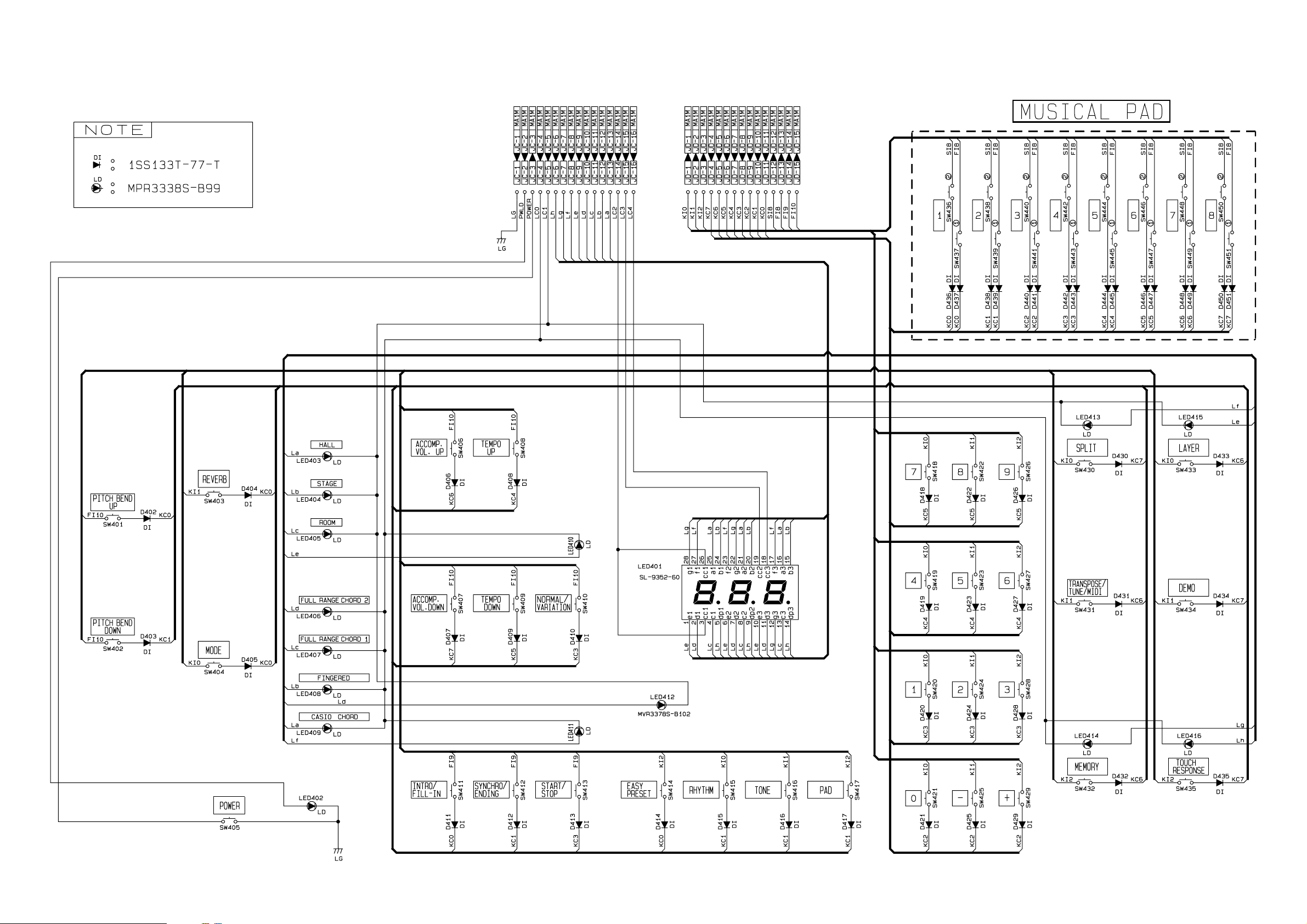
Console PCB JCM461-CN1M
— 14 —
Page 15

Keyboard PCBs JCM617T-KY1M/KY2M
— 15 —
Page 16

13
EXPLODED VIEW
15
14
12
12
7
5
4
6
3
1
2
16
8
9
10
17
18
— 16 —
19
11
20
21
21-2
22
23
27
21-1
24
25
26
Page 17

PARTS LIST
CTK-630
Notes: 1. Prices and specifications are subject to change with-
out prior notice.
2. As for spare parts order and supply, refer to the
"GUIDEBOOK for Spare parts Supply", published
seperately.
3. The numbers in item column correspond to the same
numbers in drawing.
Page 18

FOB Japan
N Item Code No. Parts Name Specification Q N.R.Yen R
Unit Price
Main PCB
N 11 6923 7120 PCB ass'y JCM461-MA1M M140225*1 1 7,920 A
N LSI101 2012 0441 LSI, DSP HG51B227FB 1 530 A
N LSI102/103 2012 0434 LSI, RAM SRM2264LM90 2 280 A
N LSI104 2012 0707 LSI, ROM MX23C1610MC-12CA20 1 1,300 A
LSI105 2012 0168 LSI, CPU UPD912GF-3BA 1 750 A
IC101 2114 2891 IC LA4598 1 140 A
IC102 2105 4249 LSI, DAC UPD6379GR 1 150 A
IC103 2114 3318 IC BA612 1 98 B
IC104 2114 1421 IC PC900V 1 210 B
IC105 2105 3941 IC RE5VA35AA-TZ 1 44 B
IC106 2105 2919 IC HD74HC4066P 1 39 B
Q101, Q103 2251 0469 Transistor 2SB1237Q.R-TV6-T 2 24 A
Q102, Q104, 2220 1387 Transistor 2SC1740SQ-TP-T
11
13 B
Q106,
Q108/109,
Q118~123
Q105 2253 0357 Transistor 2SD2008Q.R-T105-T 1 30 A
Q107 2200 4409 Transistor 2SA933-SQ-TP-T 1 14 B
Q110~117 2259 1883 Digitasl transistor DTA114TS-TP-T 8 10 B
Q124 2253 0448 Transistor 2SD1858Q.R-TV6-T 1 24 A
D101, D104
2360 1946 Zener diode MTZJ5.6C-77-T
2
8A
D102 2390 1316 Diode SB10-04A3-BT-T 1 28 B
D103 2360 1085
D105,
2390 1344 Diode 1SS133T
Zener diode
HZS6B1LTD-T 1 10 B
5
3B
D108~111
D106 2390 0371 Diode DSK10B-BT-T 1 11 B
D107 2360 2079
Zener diode
MTZJ4.7A-77-T 1 8 A
C194~196 2845 0168 Module capacitor CNB8X101K 3 58 C
J101 3501 7049 Jack, Power HEC2305-01-330
129A
J102 3612 0517 Jack YKB21-5005 1 100 B
J103
3612 0789 Jack YKB21-5010
1
60 B
J104/105 3501 9506 Jack, DIN YKF51-5030 1 75 C
VR101 2765 1344 Volume EWA-MJCC25B23 1 110 B
X101 2590 0203 Ceramic oscillator CSA16.00MX040 1 100 B
X102 2590 2009 Crystal oscillator HC-49/U20A 1 110 B
Console PCB
N 10 6923 7130 PCB ass'y, JCM461-CN1 M140227*1 1 540 B
D402~451 2390 1344 Diode 1SS133T 50 3 C
LED401 2370 1141 LED SL-9352-60 1 200 C
LED402~411, 2370 1106 LED MPR3338S-B99
14
24 C
LED413~416
LED412
2370 1190
LED
MVR3378S-B102
1
30 C
Keyboard PCBs
25 6923 6940 PCB ass'y M617T-KY1M M140211*1 1 750 B
D501~D564 2301 0101 Diode 1S2473-T-77-T 64 8 C
24 6923 6950 PCB ass'y M617T-KY2M M140212*1 1 710 B
D565~D622 2301 0101 Diode 1S2473-T-77-T 58 8 C
Mechanical Parts
N 1 6923 7210 Plastic button M240100-1
2 6922 2680 Rubber button M312082-2 1
3 6923 4340
Rubber button
M312082-3
4 6923 4331 Rubber button M312088A-2 1
N
5 6923 5030 Rubber button M312081-2 1
1
1
20 C
29 B
30 B
100 B
60 B
Notes: N – New parts
M – Minimum order/supply quantity
R – Rank
— 17 —
Page 19

FOB Japan
N Item Code No. Parts Name Specification Q N.R.Yen R
Unit Price
N 6 6923 7200
N 7 6923 7190
Rubber button
Rubber button
N 8 6923 4740 Button contct rubber M240152-1
12 3831 0833 Speaker S12J49A
N 13 6923 7181 Top panel M240217A*1
14 6921 5040 Volume knob M311860-1
N 15 6923 7170 Window M340085-1
16 6922 2840 White key set, CEGB M111723-1
17 6922 2860 White key set, DFAS M111725-1
18 6922 2850 White key set, DFA M111724-1
19 6922 2750 Black key set, 5-Key M111726-2
20 6922 2740 Black key set,10-Key M111726-1 2
21 6923 7060 Case M140171*1 1
21-1 6902 6140 Battery spring, (-) M41226-1
21-2 6903 2150 Battery spring, (+) M41330-1
22 6922 2771 Contact rubber, 32-Contact M211705A-1
23 6922 2761 Contact rubber, 30-Contact M211704A-1
26 6923 7000 Bottom plate M240116-1
27 6918 1636 Battery cover M311164F*1
M240099-1
M240098-1
1
1
1
1
1
1
1
5
1
4
1
60 B
60 B
60 B
400 B
300 C
13 B
250 C
100 A
100 A
100 A
86 A
120 A
2,470 C
1
1
1
27 B
18 B
91 B
189B
1 630 C
1 200 B
Accessory
6916 7880 Music stand M310827-1 1 120 B
Notes: N – New parts
M – Minimum order/supply quantity
R – Rank
— 18 —
Page 20

MA0800951A
 Loading...