

Page 1
CTK-330
PIANO
00
PIANO 1
01
PIANO 2
02
HONKY-TONK
03
STUDIO PIANO
04
ELEC PIANO 1
05
ELEC PIANO 2
06
ELEC PIANO 3
07
ELEC PIANO 4
08
HARPSICHORD
09
CLAVELECTRO
SYNTH-SOUND 2
70
PEAL DROP
71
COSMIC SOUND
72
SOUNDTRACK
73
SPACE PAD
74
SYNTH-SFX
75
SE 1 (VEHICLE)
76
SE 2 (TELEPHONE)
77
SE 3 (SPACE)
78
SE 4 (INVADER)
79
SE 5 (FUNNY)
GUITAR/BASS
20
GUT GUITAR
21
ACOUS GUITAR
22
JAZZ GUITAR
23
ELEC GUITAR
24
MUTE GUITAR
25
DIST GUITAR
26
WOOD BASS
27
ELEC BASS
28
SLAP BASS
29
BANJO
SPLIT/PERCUSSION
90
BRASS/PIANO
91
BRASS/E.PIANO
92
BRASS/VIB
93
BRASS/G.GUITAR
94
BRASS/D.GUITAR
95
STRINGS/PIANO
96
STRINGS/TRUMPET
97
VIBRAPHONE
98
MARIMBA
99
PERCUSSION
100 TONES
STRINGS/ENSEMBLE
30
VIOLIN
31
CELLO
32
HARP
33
STRINGS 1
34
STRINGS 2
35
STRINGS 3
36
SYNTH-STR 1
37
SYNTH-STR 2
38
CHIOR
39
VOICE
POWER/MODE
ON
OFF
BRASS
40
TRUMPET
41
TUBA
42
BRASS SECTION
43
FRENCH HORN 1
44
FRENCH HORN 2
45
BRASS 1
46
BRASS 2
47
SYNTH-BRASS 1
48
SYNTH-BRASS 2
49
SYNTH-BRASS 3
FINGERED
CASIO CHORD
NORMAL
REED/PIPE
50
SOPRANO SAX
51
ALTO SAX
52
TENOR SAX
53
OBOE
54
CLARINET
55
PICCORO
56
FLUTE
57
RECORDER
58
FLUTE ENSEMBLE
59
WHISTLE
VOLUME SYNCHRO/
SYNTH-SOUND 1
60
SYNTH-LEAD 1
61
SYNTH-LEAD 2
62
SYNTH-LEAD 3
63
SYNTH-CALLIOPE
64
SYNTH-PAD 1
65
SYNTH-PAD 2
66
SYNTH-PAD 3
67
GRASS HARMONICA
68
COUNTRY FARM
69
SYNTH-BASS
START/
TEMPO
FILL-IN
STOP
TRANSPOSE/
TUNE
TONE
RHYTHM
ORGAN
10
ELEC ORGAN 1
11
ELEC ORGAN 2
12
ELEC ORGAN 3
13
ELEC ORGAN 4
14
CHURCH ORGAN
15
PIPE ORGAN
16
REED ORGAN
17
ACCORDION
18
BANDONEON
19
HARMONICA
LAYER
80
STRINGS PIANO
81
STRINGS EP
82
CHOIR EP
83
CHOIR ORGAN
84
STRINGS GUITAR
85
STRINGS HARP
86
BRASS STRINGS
87
VIB PAD
88
12 STR GUITAR
89
CHOIR STRINGS
ELECTRIONIC KEYBOARD
MULTI FUNCTION DISPLAY
0
516273849
POPS
00
POP FUSION
01
BALLAD
02
POP BALLAD
03
RAP POP
04
SOUL BALLAD
05
FUNKY POP
06
16 BEAT
07
8 BEAT 1
08
8 BEAT 2
09
POPS
SONG
BANK
MELODY
ON/OFF
50 RHYTHMS 20 SONG BANK
ROCK
JAZZ/DANCE
EUROPEAN/LATIN
10
ROCK WALTZ
11
SLOW ROCK
12
SOFT ROCK 1
13
SOFT ROCK 2
14
FOLKIE POP
15
60' S SOUL
16
ROCK
17
HEAVY METAL
18
50'S ROCK
19
CHICAGO BLUES
20
21
22
23
24
25
26
27
28
29
BIG BAND
SLOW SWING
FOX TROT
JAZZ WALTZ
ACID JAZZ
LATIM FUSION
TRANCE
DISCO
RAP
FUNK
30
31
32
33
34
35
36
37
38
39
POLKA
MARCH
SLOW WALTZ
WALTZ
TANGO
BOSSA NOVA
SAMBA
MAMBO
RHUMBA
CHA-CHA-CHA
VARIOUS
40
41
42
43
44
45
46
47
48
49
MERENGUE
RAGGAE
SKA
TEX-MEX
FOLKLORE
COUNTRY
SLOW GOSPEL
ADANI
BAROQUE
ENKA
00
SERENADE "EINE KLEINE NACHTMUSIK"
01
TWINKLE TWINKLE LITTLE STAR
02
ACH DU LIEBER AUGUSTIN
03
AMAZING GRACE
04
ODE TO JOY
05
LONDON BRIDGE
06
LONDONDERRY AIR
07
GREENSLEEVES
08
AULD LANG SYNE
09
JOY TO THE WORLD
10
JINGLE BELLS
O CHRISTMAS TREE
11
YANKEE DOODLE
12
13
SANTA LUCIA
14
WHEN THE SAINTS GO MARCHING IN
15
ALOHA OE
16
SPRING FROM "THE FOUR SEASONS"
17
LITTLE BROWN JUG
18
MARCH FROM "THE NUTCRACKER"
19
THE ENTERTAINER
CTK-330
Page 2

CONTENTS
Specifications .......................................................................................................................... 2
Block Diagram......................................................................................................................... 3
Circuit Description ................................................................................................................... 4
Major Waveforms .................................................................................................................... 7
Schematic Diagrams ...............................................................................................................8
Printed Circuit Board .............................................................................................................10
Exploded View ...................................................................................................................... 11
Parts List ............................................................................................................................... 13
SPECIFICATIONS
GENERAL
Number of keys: 49
Polyphonic: 12-note
Preset tones: 100
Auto-rhythms: 50, Tempo control: 40 to 255
Accompaniment: Casio Chord, Fingered
Song bank: 20-tune
Tuning control: 440 Hz ± 50 cents
Built-in speakers: 4 inch dia. 2 W input rating: 2 pcs
Terminals: Stereo standard Jack (Output impedance: 100 ohm, Output voltage: 3 V (rms)
MAX
Power source: 2-way AC or DC source
AC: AC adapter
DC: 6 AA size dry batteries
Power consumption: 7.2 W
Dimensions(HWD): 988 × 311 × 125 mm (38-15/16 × 12-1/4 × 4-15/16 inches)
Weight: 3.5 kg (7.7 lbs) excluding batteries
ELECTRICAL
Current drain with 9 V DC:
No sound output 120 mA ± 30%
Maximum volume 650 mA ± 30%
with white keys C1 to G2 pressed in Synth-Lead 1
Volume: 9
Phone output Level (Vrms with 8 ohm load each channel):
with key E3 pressed in Synth-Lead 1 80 mV ± 30%
Sound Pressure (at 10 cm away from speaker):
with key E3 pressed in Synth-Lead 1 100 dB ± 10 dB
Minimum operating voltage: 6.0 V
— 2 —
Page 3
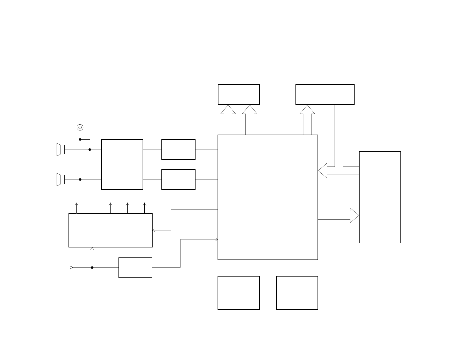
BLOCK DIAGRAM
— 3 —
Output
Power Amp.
LA4598
IC101
VC AVDD DVDD LVDD
Power Supply Circuit
Q101 ~ Q104, D106
DC+9V IN
Q111
Filter (L)
Q105
Filter (R)
Q106
APO
CC1 ~ CC3
LED
MSM 6755B-08
La ~ Lg,
Lp
CPU
LSI101
KO8 ~
KO11
Buttons
KI0 ~ KI7
Keyboard
KO0 ~ KO7
Reset IC
IC102
Oscillator
X101, Q107
Page 4
CIRCUIT DESCRIPTION
KEY MATRIX
KI0 KI1 KI2 KI3 KI4 KI5 KI6 KI7
KO0 C2 G#2 E3 C4 G#4 E5 C6
KO1 C#2 A2 F3 C#4 A4 F5
KO2 D2 A#2 F#3 D4 A#4 F#5
KO3 D#2 B2 G3 D#4 B4 G5
KO4 E2 C3 G#3 E4 C5 G#5
KO5 F2 C#3 A3 F4 C#5 A5
KO6 F#2 D3 A#3 F#4 D5 A#5
KO7 G2 D#3 B3 G4 D#5 B5
KO8 0 1 2 3 4 Start/Stop
KO9 56789
KO10 Tone Rhythm
Song
Bank
Melody
On/Off
KO11 Fingered
Tempo
Down
CASIO
Chord
Tempo UpVolume
Volume
Down
Normal Power Off
NOMENCLATURE OF KEYS
C#2 D#2 F#2 G#2 A#2 C#3 D#3 F#3 G#3 A#3 C#4 D#4 F#4 G#4 A#4 C#5 D#5 F#5 G#5 A#5
Up
Synchro/
Fill-In
C2
D2 E2 F2 G2 A2 B2 C3 D3 E3 F3 G3 A3 B3 C4 D4 E4 F4 G4 A4 B4 C5 D5 E5 F5 G5 A5 B5 C6
— 2 —
Page 5
CPU (LSI101: MSM6755B-06)
The CPU contains a sound data ROM and a DAC (Digital to Analog Convertor), and it provides left and right
channel sound waveforms in accordance with the pressed key and the selected tone.
The following table shows the pin functions of LSI101.
Pin No. Terminal In/Out Function
1 ~ 29 MA14 ~ NC2 — Not used.
30 DGND In Ground (0 V) source
31 DVCC In +5 V source
32, 33 XTLO, XTLI In/Out 20 MHz clock input/output
3 4 NC3 — Not used. Connected to ground.
35 RSTB In Reset signal input
3 6 P24/RXD — Not used. Connected to +5 V.
3 7 P25/TXD — Not used.
38 NMI In Power on signal input. Connected to +5 V.
39 APO Out APO (Auto Power Off) signal output
4 0 NC4 — Not used.
41 REFH Out Terminal for the built-in DAC
42, 43 NC5, NC6 — Not used.
4 4 DAOR Out Right channel sound waveform output
4 5 NC7 — Not used.
46 AVdac In +5 V source for the built-in DAC and ADC
47 DAOL Out Left channel sound waveform output
4 8 REFL Out Terminal for the built-in DAC and ADC
49 AGdac In Ground source for the built-in DAC
50 AGadc In Ground source for the built-in ADC
5 1 ANI — Not used. Connected to ground.
52 AVadc In +5 V source for the internal ADC
5 3 NC8 — Not used. Connected to +5 V.
54 MOD0 In Mode selection terminal
55, 56 MOD1, MOD2 In Mode selection terminal
57 KO9/P40 In APO cancelation signal input
58 ~ 65 KI0/P30 ~ KI7/P37 In Terminals for key/button input signal
66 ~ 73 KO1/P50 ~ KO8/P57 O ut Terminals for key scan signal
74 ~ 77 P20 ~ P23 Out Terminals for button scan signal
7 8 NC9 — Not used.
79 LVCC In +5 V source
80 ~ 8 2 CC1 ~ CC3 Out LED common signal output
83 ~ 87 — — Not used.
88 ~ 95 La ~ Lg, Lp Out LED segment signal output
96 LGND In Ground (0 V) source
97 ~ 100 — — Not used.
FILTER BLOCK
Since the sound signal from the CPU is a stepped waveform, the filter block is added to smooth the waveform.
Amp.
LA4598
Filter
Block
— 3 —
CPU
MSM6755B-08
Page 6

POWER AMPLIFIER (IC101: LA4598)
The power amplifier is a two-channel amplifier with standby switch.
The following table shows the pin function of IC101.
Pin No. Terminal In/Out Function
1 Power GND In Ground (0 V) source
2 Ch1 B.S. — Terminal for a bootstrap capacitor
3 Ch1 OUT Out Channel 1 output
4 VCC In +9 V source
5 Ch1 N.F. In Negative feedback input
6 Ch1 IN In Channel 1 input
7 D.C. — Terminal for a decoupling capacitor
8 Pre GND In Ground (0 V) source
9 Stand by In Power control signal input. 0 V: Off, +9 V: On
10 Ch2 IN In Channel 2 input
11 Ch2 N.F. In Negative feedback input
12 Ch2 OUT Out Channel 2 output
13 Ch2 B.S. — Terminal for a bootstrap capacitor
14 NC — Not used
LED DRIVING
Q106~Q108
LED Driver
LVDD
La~Lg, Lp
CPU
LSI101
MSM6755B
CC1~CC3
— 4 —
Page 7

CPU (LSI101: MSM6755B-06)
The CPU contains a sound data ROM and a DAC (Digital to Analog Convertor), and it provides left and right
channel sound waveforms in accordance with the pressed key and the selected tone.
The following table shows the pin functions of LSI101.
Pin No. Terminal In/Out Function
1 ~ 29 MA14 ~ NC2 — Not used.
30 DGND In Ground (0 V) source
31 DVCC In +5 V source
32, 33 XTLO, XTLI In/Out 20 MHz clock input/output
3 4 NC3 — Not used. Connected to ground.
35 RSTB In Reset signal input
3 6 P24/RXD — Not used. Connected to +5 V.
3 7 P25/TXD — Not used.
38 NMI In Power on signal input. Connected to +5 V.
39 APO Out APO (Auto Power Off) signal output
4 0 NC4 — Not used.
41 REFH Out Terminal for the built-in DAC
42, 43 NC5, NC6 — Not used.
4 4 DAOR Out Right channel sound waveform output
4 5 NC7 — Not used.
46 AVdac In +5 V source for the built-in DAC and ADC
47 DAOL Out Left channel sound waveform output
4 8 REFL Out Terminal for the built-in DAC and ADC
49 AGdac In Ground source for the built-in DAC
50 AGadc In Ground source for the built-in ADC
5 1 ANI — Not used. Connected to ground.
52 AVadc In +5 V source for the internal ADC
5 3 NC8 — Not used. Connected to +5 V.
54 MOD0 In Mode selection terminal
55, 56 MOD1, MOD2 In Mode selection terminal
57 KO9/P40 In APO cancelation signal input
58 ~ 65 KI0/P30 ~ KI7/P37 In Terminals for key/button input signal
66 ~ 73 KO1/P50 ~ KO8/P57 O ut Terminals for key scan signal
74 ~ 77 P20 ~ P23 Out Terminals for button scan signal
7 8 NC9 — Not used.
79 LVCC In +5 V source
80 ~ 8 2 CC1 ~ CC3 Out LED common signal output
83 ~ 87 — — Not used.
88 ~ 95 La ~ Lg, Lp Out LED segment signal output
96 LGND In Ground (0 V) source
97 ~ 100 — — Not used.
FILTER BLOCK
Since the sound signal from the CPU is a stepped waveform, the filter block is added to smooth the waveform.
Amp.
LA4598
Filter
Block
— 5 —
CPU
MSM6755B-08
Page 8

POWER AMPLIFIER (IC101: LA4598)
The power amplifier is a two-channel amplifier with standby switch.
The following table shows the pin function of IC101.
Pin No. Terminal In/Out Function
1 Power GND In Ground (0 V) source
2 Ch1 B.S. — Terminal for a bootstrap capacitor
3 Ch1 OUT Out Channel 1 output
4 VCC In +9 V source
5 Ch1 N.F. In Negative feedback input
6 Ch1 IN In Channel 1 input
7 D.C. — Terminal for a decoupling capacitor
8 Pre GND In Ground (0 V) source
9 Stand by In Power control signal input. 0 V: Off, +9 V: On
10 Ch2 IN In Channel 2 input
11 Ch2 N.F. In Negative feedback input
12 Ch2 OUT Out Channel 2 output
13 Ch2 B.S. — Terminal for a bootstrap capacitor
14 NC — Not used
LED DRIVING
Q106~Q108
LED Driver
LVDD
La~Lg, Lp
CPU
LSI101
MSM6755B
CC1~CC3
— 6 —
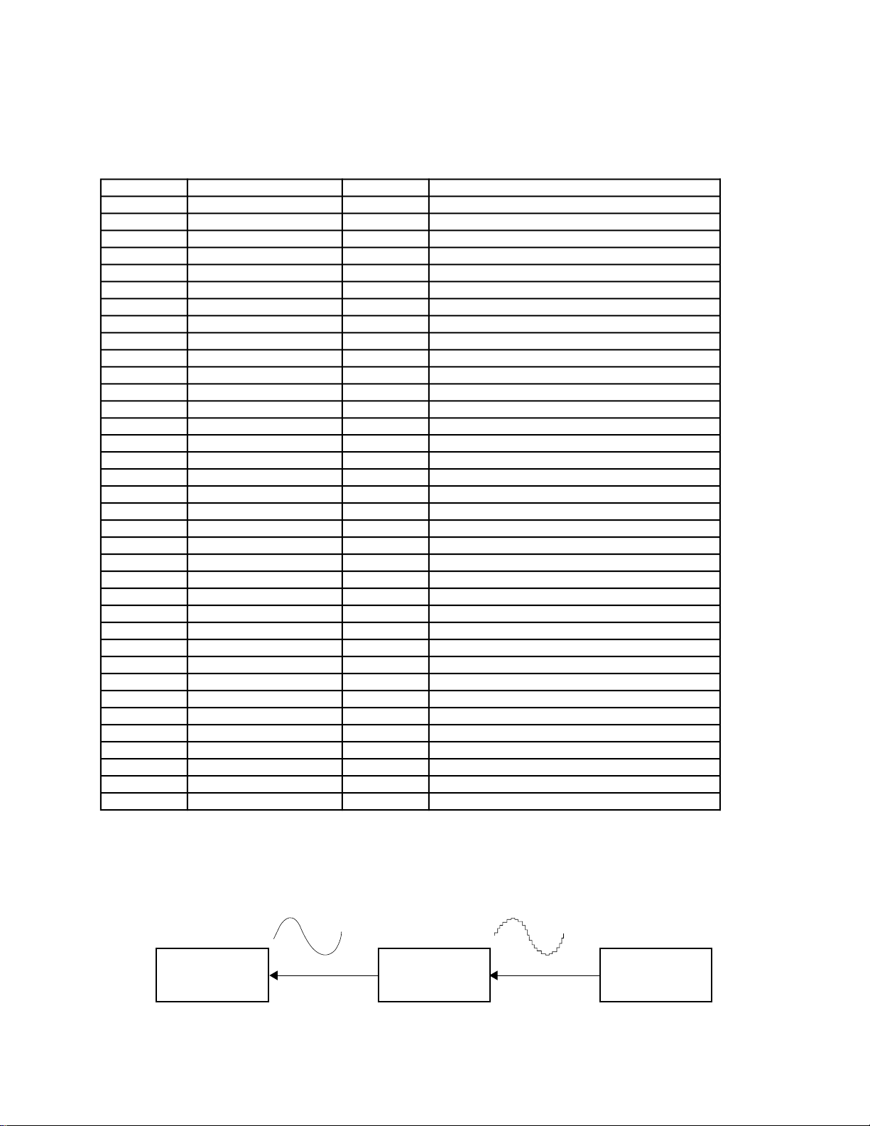
Page 9

MAJOR WAVEFORMS
1
1 Clock pulse
MSM6755B-08 pin 32
4
2
3
2 Reset signal
MSM6755B-08 pin 35
3 APO signal
MSM6755B-08 pin 39
6
7
5
4 Sound waveform (R-ch)
MSM6755B-08 pin 44
5 Sound waveform (L-ch)
MSM6755B-08 pin 47
8
9
8 LED common signal CC2
MSM6755B-08 pin 81
9 LED common signal CC3
MSM6755B-08 pin 82
Tone: whistle
Key: A4
Volume:
6 Button scan signal KO10
MSM6755B-08 pin 76
7 Button scan signal KO11
MSM6755B-08 pin 77
— 7 —
Page 10

Main PCB KDM441-MA1M/MA2M
1
23
5
4
7
6
9
8
SCHEMATIC DIAGRAMS
— 8 —
Page 11

Keyboard PCBs KDM4910K-KY1M/KY2M
— 9 —
Page 12

Main PCB KDM441-MA1M
PRINTED CIRCUIT BOARD
4 52316789
— 10 —
Page 13

EXPLODED VIEW
12
11
13
R-1
4
10
3
9
5
R-2
1
14
8
14
6
R-6
7
2
R-4
R-3
R-5
— 11 —
Page 14

PARTS LIST
CTK-330
Notes: This parts list does not include the cosmetic parts, which
parts are marked with item No. "R-X" in the exploded
view.
Contact our spare parts department if you need these
parts for refurbish.
1. Prices and specifications are subject to change without prior notice.
2. As for spare parts order and supply, refer to the
"GUIDEBOOK for Spare parts Supply", published
seperately.
3. The numbers in item column correspond to the same
numbers in drawing.
Page 15

Item Code No. Parts Name Specification Q R
Main PCB
1 6925 4480 Main PCB ass'y M441-MA1,2M M140451*1 1 B
LSI101 2012 3948 LSI, CPU MSM6755B-08 1 A
IC101 2114 2891 IC, Amp. LA4598 1 A
IC102 2105 5922 IC RE5VL40AA-TZ 1 A
Q101 2250 0168 Transistor 2SA854SR-TP-T 1 A
Q102, Q105 - Q110, 2220 1387 Transistor 2SC1740SQ-TP-T 8 A
Q112
Q103, Q104 2253 0448 Transistor 2SD1858Q,R-TV6-T 2 A
Q111 2200 2449 Transistor 2SA933SQ-TP-T 1 A
D101 2390 0371 Diode DSK10B-BT-T 1 B
D102 2390 1323 Diode RB100A-T32-T 1 B
D103, D105, 2390 1344 Diode 1SS133T-77-T 23 C
D107 - D127
D106 2360 2002 Diode, Zener MTZJ5.6B-T77-T
D128 2390 2828 Diode RB441Q-40T-77
D133 2360 1715 Diode, Zener MTZJ3.9B-T77-T
LED101 2370 1309 LED LB-603VF1 1 B
X101 2590 1526 Ceramic oscillator EFO-EN2005C4 1 B
J101 3501 7049 Jack, Power HEC2305-01-330
J102 3612 0665 Jack, Phone YKB21-5006 1 C
Keyboard PCB
2 6925 4490 Keyboard PCB ass'y M140449*1 1 C
D701 - D749 2301 0101 Diode 1S2473T-77-T 49 B
Mechanical Parts
3 6922 2720 White key set, LT-CB M312118*1 3
4 6922 2730 White key set, LT-CS
5 6922 2740 Black key set, LT-10P M111726-1 2
6 6922 4000 Key contact rubber, 31-contact M111765-1
7 6923 2390 Key contact rubber, 18-contact M240025-1
8 6925 4500 Battery cover M340528*1
9 6925 4510 Rubber button M240463-1
10 6925 4520 Rubber button M240464-1
11 6909 5890 Slide contact CSB-12D
12 6921 5030 Slide knob M311859-1
13 6925 4530 Display plate M340511-1 1
14 3831 0770 Speaker S10JA13A
Accessory
6916 7880 Music stand M310827-1
M312118*2 1
1
1
1
1
1
1
1B
1
1
1
1
2
1B
B
B
B
B
A
A
A
A
A
B
B
B
B
C
B
Notes: Q – Used quantity
R – Rank
— 13 —
Page 16

MA0800761A
Aug, 1996
 Loading...