

Page 1

P
i
4
T
S
V
S
S
V
V
P
P
4
T
4
T
FCC Infor mation and Copyright
This equipment has been tested and found to com ply with the limits of a
Class B digital device, pursuant to Part 15 of the FCC Rules. T hese limits
are designed to provide reasonable protection against harmful
int erference in a residential ins t allation. This equipment g enerat es, uses
and can radiate radio frequency energy and, if not installed and used i n
ac cordan ce wit h the in stru ction s, ma y cau se harm fu l in terf eren ce t o radi o
communications. There is no guarantee th at interference will not occur in
a partic ular installation.
The vendor makes no repr esentations or warranties with respect to the
contents here of and specially disclaims any implied
merchantabi li ty or fitness fo r a ny purpose. F urther the vendor reserves
the right to revise this publication and to make changes to the contents
here of without obligation to notify any party beforehand.
Duplication of this publication, in part or in whole, is not allowed without
first obtaining the vendor’s approval in writing.
The con tent of this user’s manual is subject to be changed without notice
and we will not be responsible for any mistakes found in this user’s
manual. All the brand and product names are trademarks of their
r es p e c t iv e co m pa ni e s.
warran ties of
Page 2

C
C
C
o
o
t
n
e
t
n
t
n
e
t
n
t
n
e
t
n
o
LAYOUT OF P4TSV.................................................................................1
COMPONENT INDEX............................................................................. 2
ENGLISH...................................................................................................3
P4TSV Features.........................................................................................3
Packag e contents.......................................................................................5
How to set up Jumper.................................................................................5
CPU Ins t alla tion......... ........................ ........................................................5
DDR DIMM Modu les: DD RA1-2, DDRB1-2......................................................6
Inst allin g DDR Module ........................................................................ ........7
Jumpers, Headers, Connectors & Slots.........................................................7
ESPAÑOL ................................................................................................14
Características del P4TSV.........................................................................14
Co nt enido del Paquete........... ........................ ........................ ..................16
Cómo instalar un Puente........................................................................... 16
Instalación del C PU..................................................................................16
Módulos DDR DIMM: DDRA1-2, DDRB1-2.................................................... 17
Instalación del Módulo DDR ......................................................................18
Puentes, C abezales, Con ectores y Ranuras................................................19
DEUT SCH................................................................................................26
Spezifikationen von P4TSV........................................................................ 26
Verpackungsinhalt...................................................................................28
Einstellung der Jumper.............................................................................28
Inst alla tion der CP U.... ........................ ........................ ........................ ......28
DDR DIMM Modu les: DD RA1-2, DDRB1-2....................................................29
Installation von DD R-Modul....................................................................... 30
Jumpers, Headers, Anschlüsse & Slots....................................................... 30
WARPSPEEDER..................................................................................... 37
Introdu ction.............................................................................................37
System Requirement................................................................................37
Installation ..............................................................................................38
Usage.....................................................................................................39
TROUBLE SHOOTIN G......................................................................... 47
SOLUCIÓN DE PROBLEMAS.............................................................48
PROBLEMLÖSUNG.............................................................................. 49
ii
Page 3
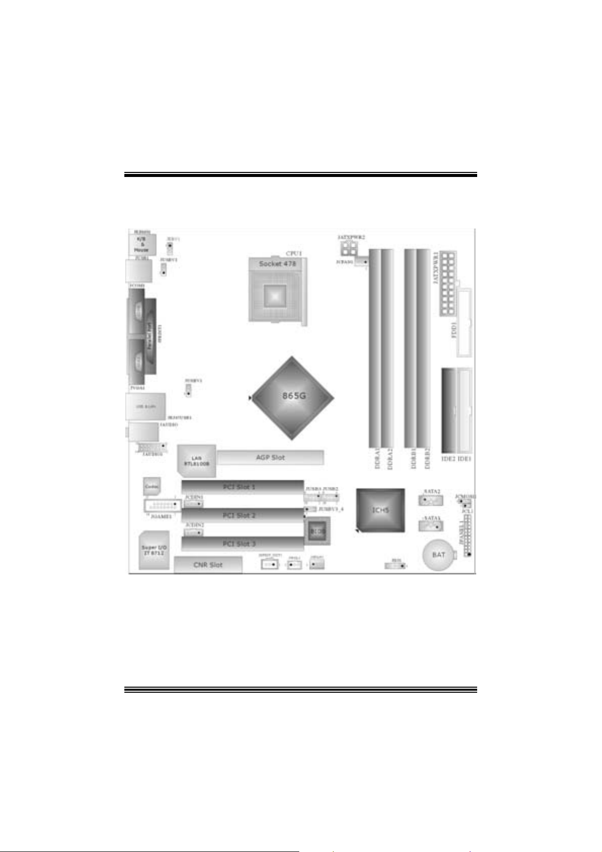
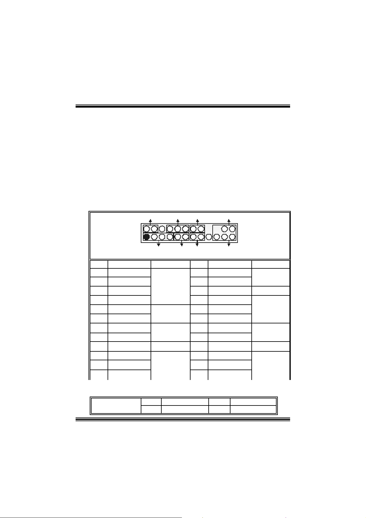
Layout of P4TSV
NOTE: ●represents the first pin.
1
Page 4
V
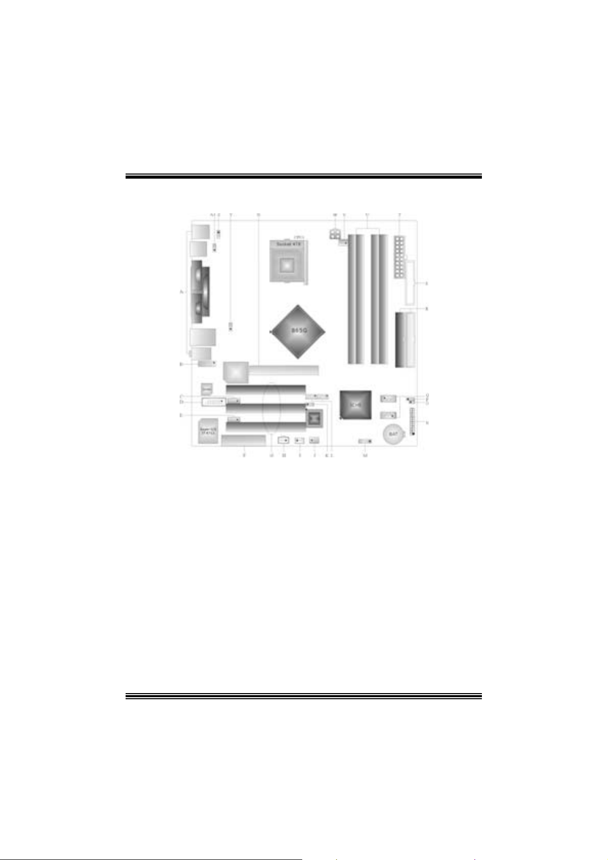
Component Index
A. B ack Panel Connectors O. JCL 1: Case Open Connector
B. JA UDIO1: Front A udio Header P. JCMOS: Clear CM OS Jumper
C. JCDIN1: CD-Rom Au dio-I n Header Q. SAT A1-2: Ser ial AT A C o nnectors
D. JGAME1: Game Head er R. ID E1-2: Hard Disk Connector s
E. JCDI N2: CD-ROM Audio-In Header S . FDD1: F loppy Disk Connector
F. CNR1: Communication Network
Ri ser Slot
G. PCI1-3: Peripheral Component
In ter conn ect Slots
H. JSPDIF_OUT1: Digital Audio
Connector
I. JW OL1: Wake On L AN Head er
J. JSF AN1: System Fan Header
K. JUSBV3_4: 5V/5VSB Selection for
JUSBV2/3
L. JUSB2/ 3: Front U SB Headers
M. JDJ1: Audio DJ Connector
N. JPANEL1 : Fr on t Pan el Connector
T. JATXPWR1: ATX Power Co nnector
U. DDRA1-2/ DDRB1-2: DDR DIMM
Modules
V. JCFAN: CPU Fan Con nector
W. JATXPWR2: ATX Power
Connector
X. AGP1: Accelerated Graphics Port
Slot
Y. JUSBV2: 5V/5VSB Selection for
JRJ45USB1
Z. JKBV1: 5
Keyboard
A1. JUSBV1: 5V/5VSB Selection for
JUSB1
/5VSB Selection for
2
Page 5

English
P4TSV Fe atur es
A. Har dware
CPU
Pr ov ide s S o cke t-478 .
Supports the Intel Pentiu m 4 proce ssor up to 3 .06GHz.
F ront Side Bus at 400/533/800MHz.
Su pports Hyper-Threading.
Support s Nort hwood and Prescott CPU. (W illamet t e not suppor ted)
Chipset
North Bridge: Intel 865G.
South Bridge: Intel ICH 5.
Main Me m o ry
Supports one or two 64-bit wide DDR data channels with 1 or 2 DIMMs
per-channel.
Av ailable bandwidt h up t o 3.2GB/s (DDR400) for single-channel mode and 6.4GB/s
(DDR 400) in dual channel mode.
Supports 128-MB, 256-Mb, 512-Mb and 1-GB DDR t ec hnologies .
Supports only x8, x16 DDR devic es.( Does not support regis t ered DIMMs or
double s ided X 16 DI MMs)
Supports four bank devices.
Maxi mu m me mo ry s i ze is 4GB.
Super I/O
Chip: ITE IT 8712F.
Low Pin C ount Int erface.
Prov ides the most commonly used legacy Super I/O f unctionality.
Env iro nm ent C ont rol i niti atives ,
- H/W Monitor
- Fan Speed Controller
- I TE's "Smart Guardian" f unction
Slots
Three 32-bit PCI bus master s lots.
On e CN R slo t .
One AGP 4X/8X slot.
On Board IDE
Supports four IDE di s k dri ves.
Supports PIO Mode 5, Bride Mode and U lt ra DMA 33/66/100 Bus Mast er Mode.
Supports 2 Serial ATA (SATA) ports.
3
Page 6

- C om pliant wit h SATA 1.0 specif ic ation
- Data transfer rates up to 1.5 GB/s
LAN
Chip: RTL8 100B.
Supports 10 Mb/s and 100 Mb/ s auto-negot iat ion.
Hal f/Full du plex cap ability.
Supports ACPI power m anagement.
On Bo ard AC’97 Sound Cod ec
Chip: C MI9739A.
Compliant with AC ’97 s pec ificat ion.
AC 97 2. 2 interf ac e.
Support s 6 c hannels.
On Board Peri pherals
a. R e ar si de
1 s erial port .
1 parallel port. (SPP/EPP/ECP m ode)
1 VGA port.
Audio ports in v ert ical.
1 R J -45 LAN jack.
Support s PS/ 2 mous e and PS/ 2 keyboard.
4 USB2.0 por t s.
b. F ront Si d e
1 floppy port supports 2 F DDs with 360K, 720K, 1.2M, 1.44M and 2. 88Mby tes.
4 USB2.0 port s.
Dimensions
Mic ro ATX Form Fac t or: 24.4 X24.4cm (W X L)
B. BIOS & S oftware
BIOS
Award legal BI OS.
Support s APM1.2.
Support s AC PI.
S upports USB Func tion.
Software
Supports Warpspeeder™ , 9th Touch™, FLASHER™, StudioFun! ™ (opt ional).
Offers the highest performance for Windows 98 SE, Windows 2000, W indows Me,
Windows XP, SC O UNIX etc.
4
Page 7
Package contents
HDD Cable X 2
FDD Cable X1
User’s Manual X1
Fully Setup Driver CD X1
St udioF un! Application CD X 1 (optional)
USB 2.0 Cable X1 (optional)
S/ PD IF Cable X 1 (optional)
Rear I/ O Panel for Mic ro ATX C as e X1 (opt ional)
Serial ATA C able X1
Se rial AT A Po w er Sw it c h C able X1
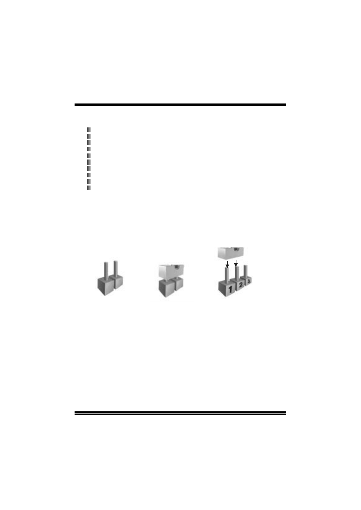
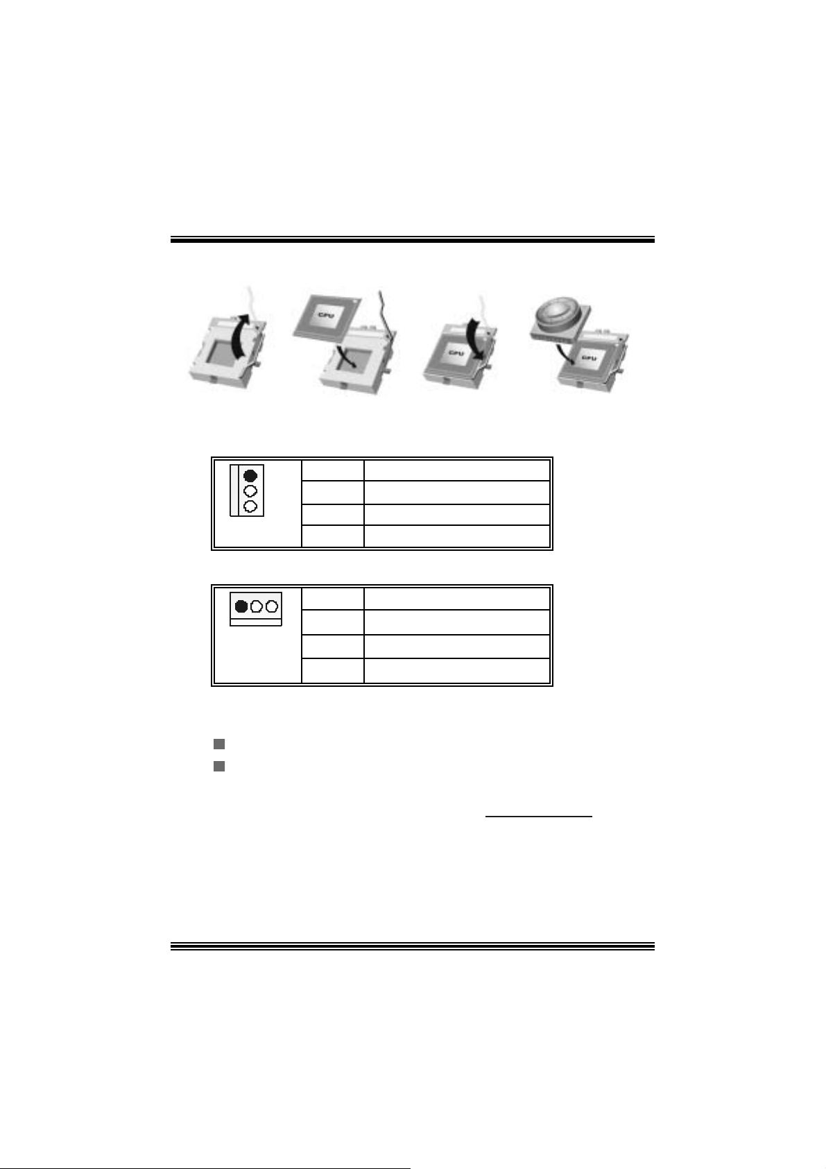
How to s e t u p Jumper
The illustration s hows to how set up jumper. When the J umper cap is placed on pins, the
jumper is “close”. IF no jumper cap is placed on the pins, the jumper is ”open”. The
illust rat ion shows a 3-pin jum per whose pin1and 2 are “close” when jumper c ap is placed
on thes e 2 pins .
Jumper open Jum per close Pin1-2 close
CPU Installation
Step1: Pull the lever sideway s away from the socket and then raise the lev er up to a
90 -degree angl e.
Step2: Look for the whit e dot /cut edge. The whit e dot/ c ut edge s hould point wards the lev er
piv ot. The C P U will f it only in th e correc t orientation.
Step3: Hold the CPU down fir mly, an d then cl ose the lever to complete the installation.
Step4: Put the CPU Fan on the C PU and buck le it. Connect the C PU fan power cable to
the JCFAN1. This completes the installation.
5
Page 8
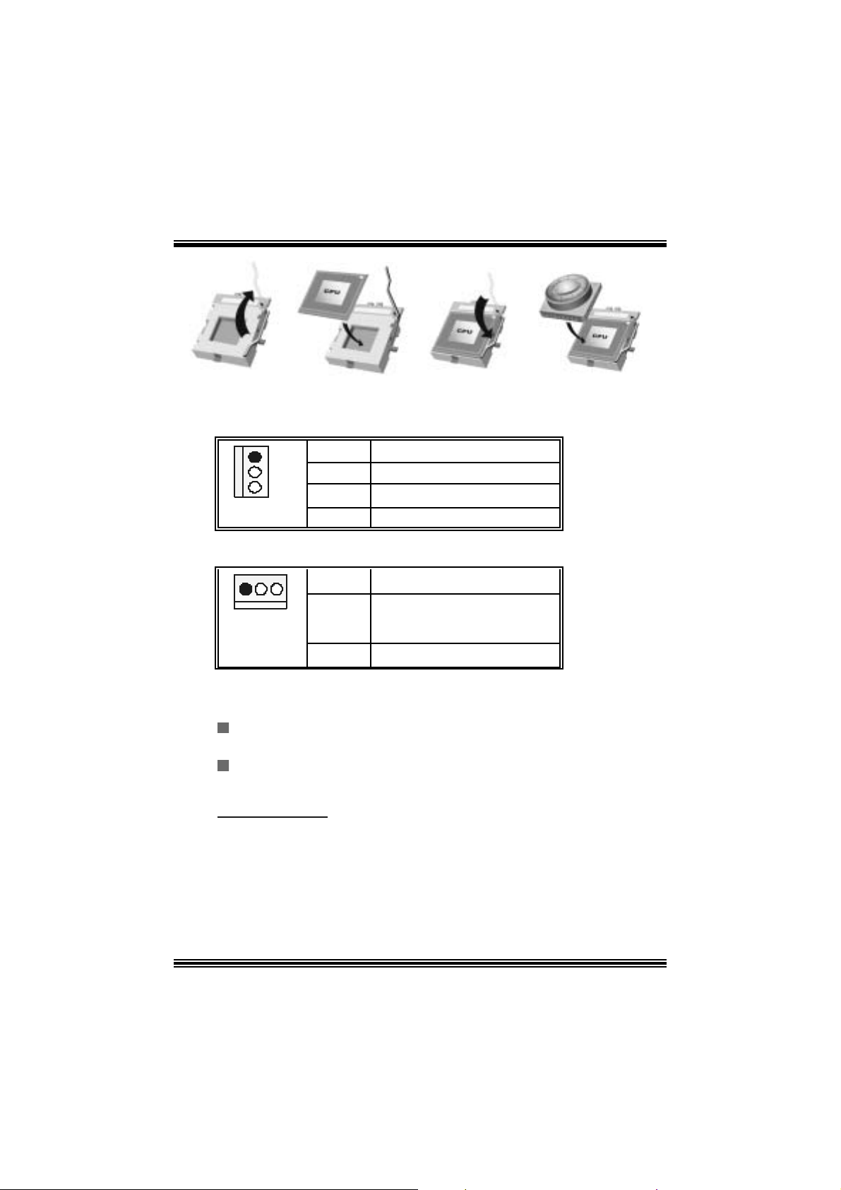
Ste p 1 Step2 Step3 Step4
CPU Fan Headers: JCFAN1
1
JCFAN1
Pin Assignment
1
2
3
Ground
+12V
FAN RPM Sense
S ystem Fan Headers: JSFAN1
Pin Assignment
1
JSFAN1
1
2
3
Ground
+12V
FAN RPM Sense
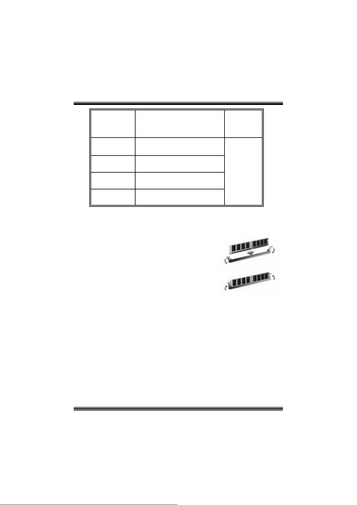
DDR DI MM Module s: DDRA1- 2, DDRB1-2
Support s up to four DD R DI MMs(two DI MMs per channel), single-s ided and/ or
double-sides.
F or Dual Channel Operat ion, DI MMs must be populated in identical pairs. It
has to be t he com bination of DDR A1+DDR B1 (Blue DIMMs) or DDRA2+DD RB2
(white DIMMs). For more dual channel operation information please log on:
www.biostar.com.tw
)
DRAM Acces s Time: 2.5V Unbuffered/ no regis tered (without ECC) DD R SDRAM
DRAM Ty pe: 128MB/ 256MB/ 512MB/ 1GB DI MM Module (184 pin)
PC2100/ PC 2700/ PC 3200 Type required.
T otal Memory Size with U nbu ffered/ R eg i s tered D I MMs
6
Page 9

DI MM Socke t
Location
DDRA1 6 4MB/128MB/256MB/512MB/1GB
DDRA2 6 4MB/128MB/256MB/512MB/1GB
DDRB1 64 MB/128 MB/2 56 MB/5 12MB/1 GB
DDRB2 64 MB/128 MB/2 56 MB/5 12MB/1 GB
DDR Mod u l e To tal Memory
Size (MB)
*1
*1
*1
*1
***O nly for referenc e***
Max is
4GB
Installing DDR Mod ule
1. Unloc k a DIMM slot by pressing the retaining clips
o ut wa rd. Ali gn a D I MM on t h e sl ot s uc h t hat t he
notc h on the DIMM matches the break on the slot.
2. Ins ert the D IMM vertically and f irm ly into the s lot
until the retaining chip snap back in place and the
DIMM i s properly seated.
Jump ers, H eade rs , Co nnectors & Slo ts
Floppy Disk Conne ctor: FDD1
The mot herboard provides a standard f loppy disk connector that supports 360K,
720K, 1.2M, 1.44M and 2.88M floppy disk types. This connector supports the
prov ided f loppy drive ribbon cables .
Hard Disk Connectors: IDE1/ IDE2
The motherboard has a 32-bit Enhanced PCI IDE Controller that provides PIO
Mode 0~5, Bus Mast er, and U ltra DMA 33/ 66/ 100 f unctionality. I t has two H DD
connectors ID E1 (primary) and IDE2 (secondary).
The ID E c onnectors can c onnect a master and a slav e driv e, so y ou can c onnect
up t o f our hard dis k driv es . The f irs t hard driv e should alway s be connected t o
IDE1.
Periphera l Component Int erconnect Slots: P CI1-3
This m ot herboard is equipped with 3 st andard PCI s lots. PCI stands for Peripheral
Component I nterconnec t, and it is a bus standard for expansion cards. This PCI
slot is des ignated as 32 bits.
Accelerate d Graphics Port Slot: AGP1
Your monitor will attach directly to that video card. This motherboard supports
7
Page 10
video cards f or PC I s lots, but it is als o equipped with an Accelerated Graphics Port
(AGP). An AGP card will take adv antage of AGP tec hnology f or improv ed video
efficiency and perform ance, es pecially with 3D graphics.
Commun ication Netwo r k R ise r Slot: CNR1
The CNR specification is an open I ndust ry St andard Architecture, and it def ines a
ha rdw ar e scalable r iser card interfa ce , which su pport s modem only.
Serial ATA Co nnector: JSATA1/JSATA2
The mot herboard has a PCI to SATA C ontroller with 2 channels SATA int erf ace, it
satisfies the SATA 1.0 spec and can transf er data wit h 1. 5GH z s peed.
Front Pane l Conne ctor: JPANEL1
SLP
JPANEL1
Pin Assignment Function Pin Assignment Function
1 +5V 2 Sleep C ont rol
3 NA 4 Ground
5 NA 6 NA NA
7 Speaker
9 HDD LED (+) 10 Power LED (+)
11 HDD LED (-)
13 Ground 14 Power Butt on
15 Reset Control
17 NA 18 KEY
19 NA 20 KEY
21 +5V 22 Ground
23 IRTX
2
123
PWR_LED
SPK
Speaker
Connector
Hard Drive
LED
Reset
Button
IrDA
Connector
HLED
RST
8 Power LED (+)
12 Power LED (-)
16 Ground
24 IRRX
IRON/OFF
IR
24
Sleep
Button
POWER
LED
Power-on
Button
IrDA
Connector
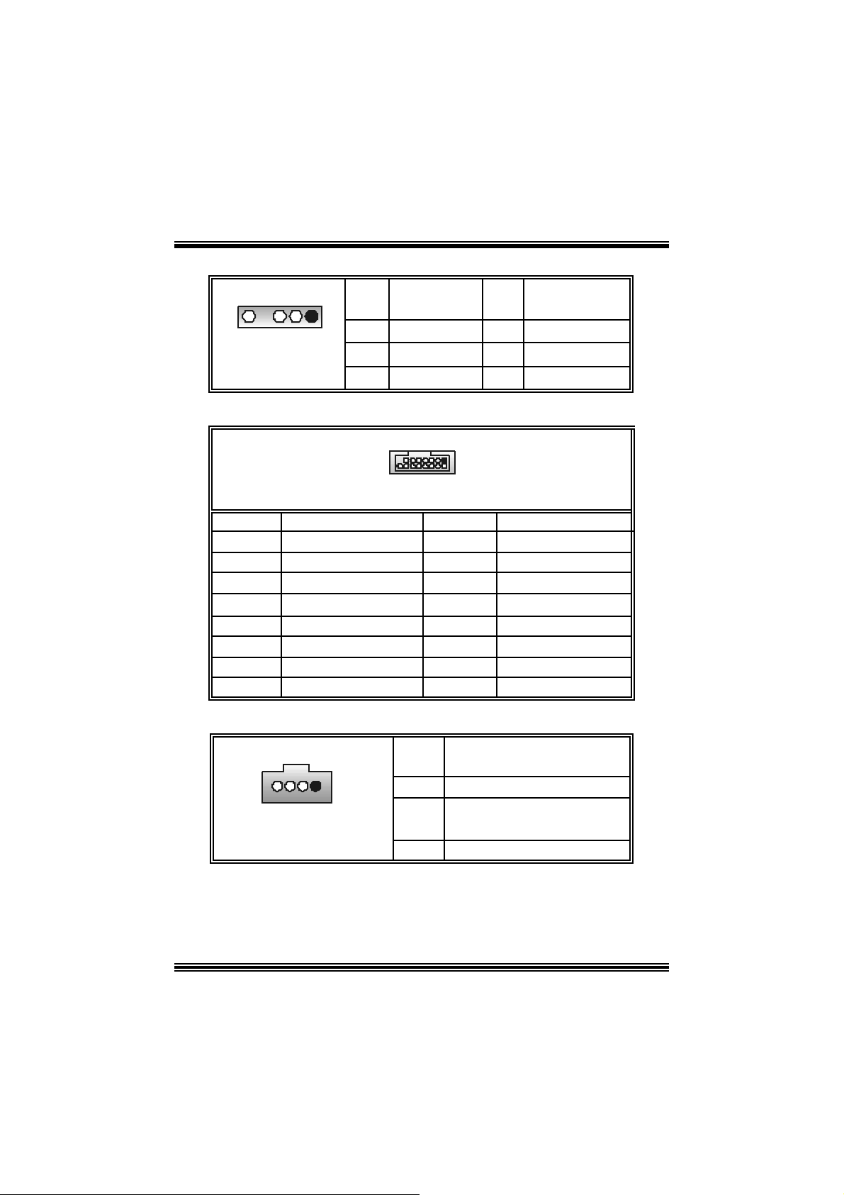
Power Conn ectors: JATXPWER1/ JATXPWR2
PIN Assignment PIN Assignment
1
+3.3V
8
11
+3. 3V
Page 11
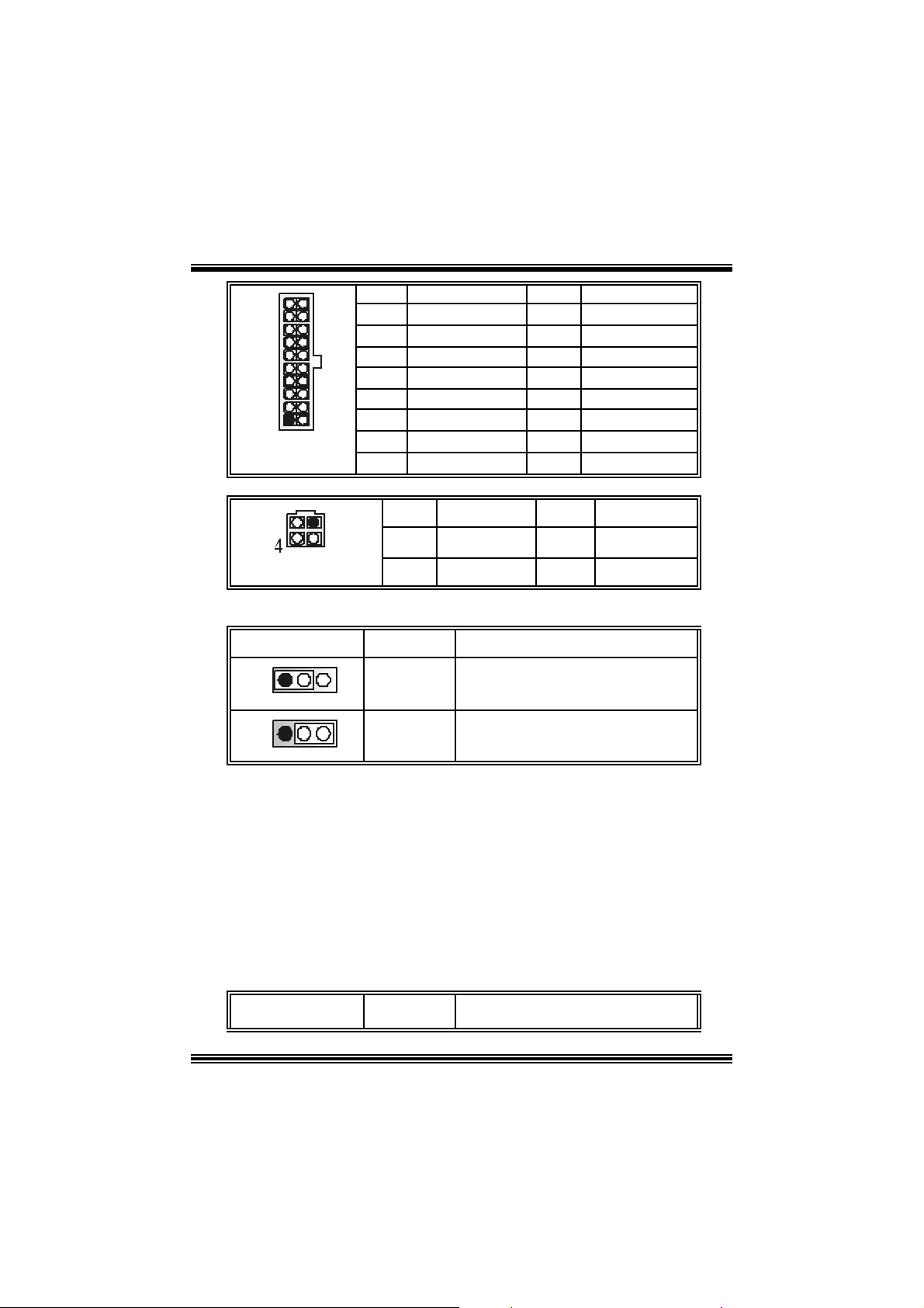
10
1
JATXPWR1
JATXPWR2
20
11
12
3
2
3
4
5
6
7
8
9
10
PIN Assignment PIN Assignment
+3.3V
Ground
+5 V
Ground
+5 V
Ground
PW_OK
+5V_SB
+1 2V
1
2 +12V 4 Ground
+12V
12
13
14
15
16
17
18
19
20
3
-12V
Ground
PS_ON
Ground
Ground
Ground
-5V
+5V
+5V
Ground
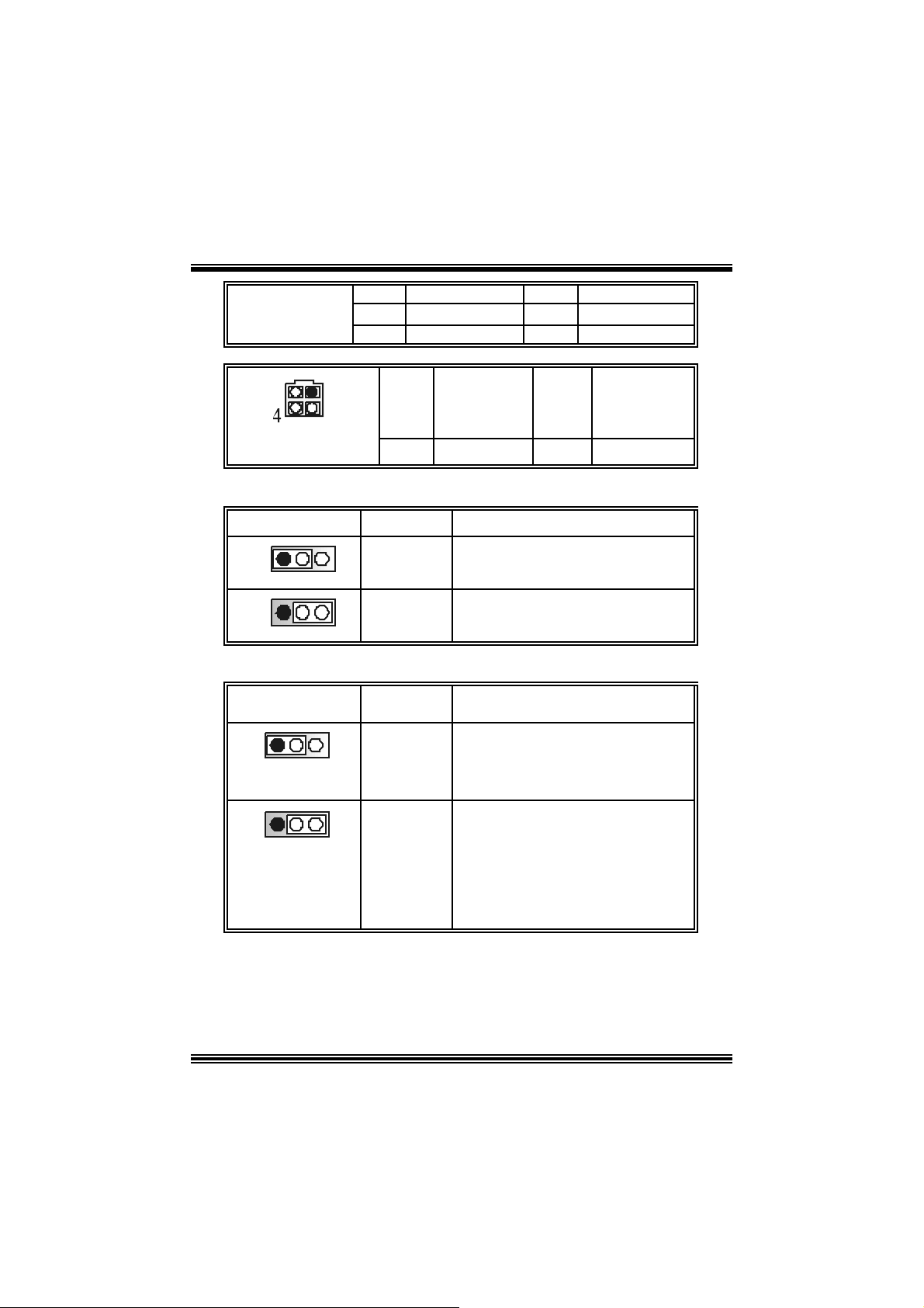
5V / 5VSB Selection for KB: JKBV1
JKBV1 Assignment Description
1 3
Pin 1-2 c los e
1 3
Pin 2-3 c los e
+5 V
+5V_SB
5V for ke yboa rd and mouse
5 V standby for keyboard and mouse to
po w er on your system
5V/ 5VSB Selection for USB: JUSBV1/ JUSBV2/J USBV3_ 4
JUSBV1/JUSBV2/
JUSBV3_4
Assignment Description
9
Page 12

1 3
Pin 1-2 c los e
1 3
Pin 2-3 c los e
+5 V
+5V_SB
5V JUSBV1 for JUSB1 port
5V JUSBV2 for J RJ45US B1 por t
5V JU SBV3_4 for JUSB2/3 ports
JU SBV1 5V standby to power on
JU SBV2 5V standby to power on
JRJ45U SBV1 port
JU SBV3_4 5V standby to power on
Clear CMOS Jumper: JCMOS1
1 3
1 3
JCMOS1 Assignment
Pin 1-2 C los e
Pin 2-3 C los e
Norm al Operation (def ault)
Clear CMOS Data
※ Clear CMOS Procedures:
1. R emov e AC power line.
2. Set the jumper to “Pin 1-2 C lose”.
3. Wa it for fi ve seconds.
4. Set the jumper to “Pin 2-3 C lose”.
5. Power on t he AC .
6. R eset your des ired password or clear t he C MOS dat a.
Ca se Op e n Connec to r: JCL1
JU SB1 port
JU SB2/3 ports
12
JCL1 2
Pin
1
Assign ment
Case Open Signal
Ground
Serial ATA Co nnector: JSATA1/ JSATA2
Pin Assignment Pin Assignment
1
Ground
10
2
TX+
Page 13
4 TX- 4 Ground
RX-
Ground
6
1234567
JSA TA1/ JSATA2
5
7
AUDIO DJ Connector: JDJ1
JDJ1
Pin Assignment Pin Assignment
SMBDATA
1
15
3
5
INT_B
ATX_PWROK
2
4
Game Header: JGAME1
JGAME1
1
216
2
4
8
10
12
14
16
Ground
Ground
15
Pin Assign m ent Pin Assignment
1
3
5 GP2 6 GP0
7
9
11
13
15
+5V
GP6
MIDI-OUTR
GP3
GP7
MIDI-INR
NA
CD-ROM Audio-In Heade r: JCDIN1/JCDIN2
1
JCDIN1/2
Pin Assignment
1
2
3
4
Left Channel In put
Ground
Ground
Right Channel In put
RX+
SMBCLK
KEY
+5V
GP4
GP1
GP5
+5V
11
Page 14

Front Panel Audio Header: JAUDIO1
2
1
JAUDIO1
Pin Assignment Pin Assignment
1
3
5
7
9
11
13
Mic In
Mic Po we r
RT Line Out
Reserved
LFT Line Out
RT Line I n
LET Line In
2
4
6
8
10
12
14
14
13
Ground
Audio Power
RT Line Out
LFT Line Out
RT Line In
LET Line I n
Digital Audio Connector: JSPDIF_OUT1
1
JSPDI F_OUT1
Pin Assignment
1
2
3
+5V
SPDIF_OUT
Ground
Wake On LAN He ader: JWOL1
1
JWO L1
Pin Assignment
1 +5V_SB
2
3 Wake up
Ground
Front USB Header: JUSB2/3
Pin Assignment Pin Assignment
10
9
1
3
5
7
9
+5V(fused)
USBP
USBP
Ground
KEY
2
4
6
8
10
2
1
JUSB2/3
Key
+5V(fused)
USBP
USBP
Ground
NC
12
Page 15
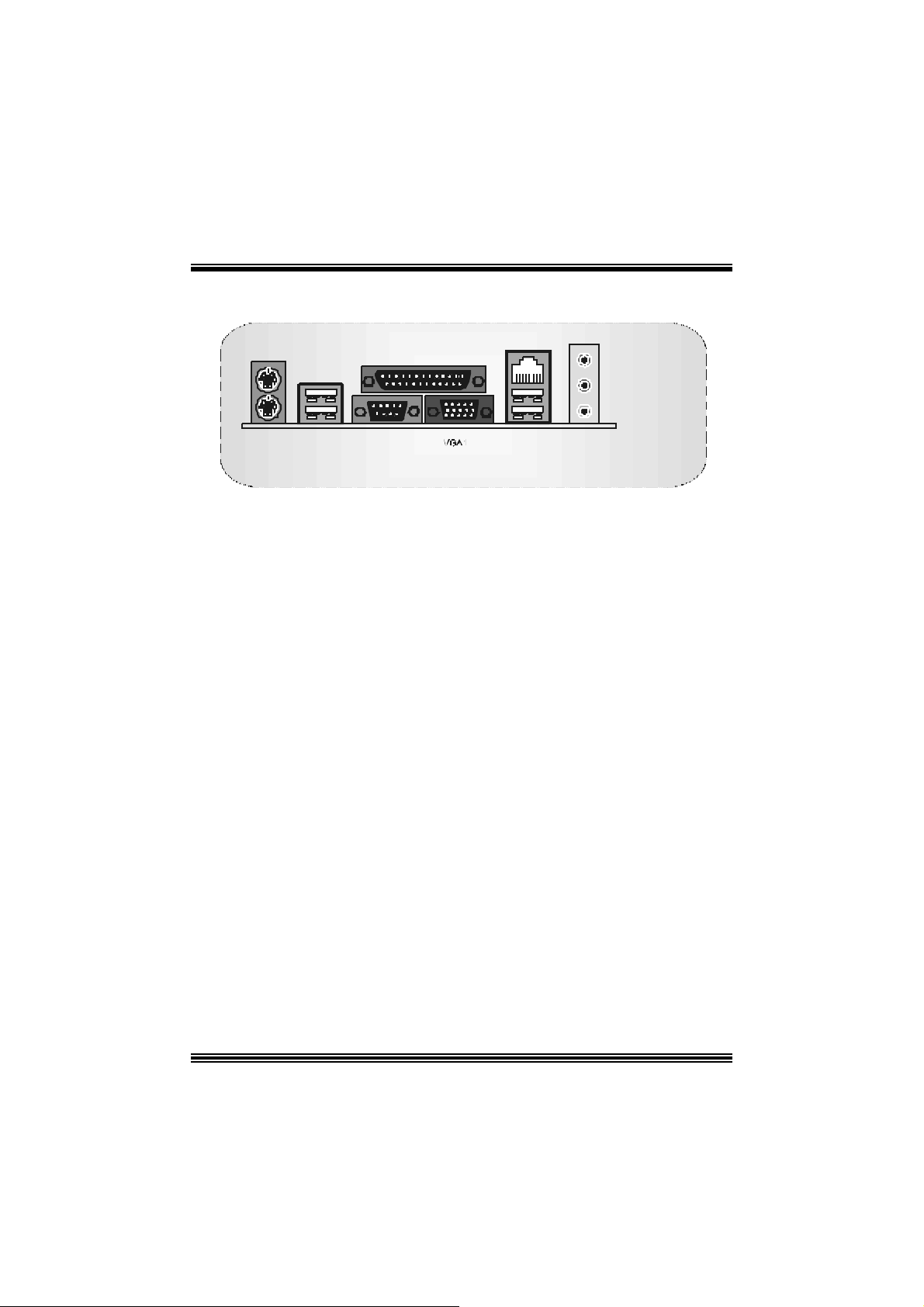
B ack Panel Connectors
Mouse
Keyboa rd
JKBMS1
USB
JUSB1
Parallel
1
1 3
COM1
JCOM1
3
JVGA1
LAN
USB
JRJ45USB1
Line In / Sur r ou nd
Speaker Out
Mic In/ Bass&Ce nter
JAU DIO
13
Page 16

Español
Características del P4TSV
A. Har dware
CPU
Pr oporcion a Soc ket-478 .
Soporta proc es ador Int el Pentium 4 de has t a 3.06GHz.
F ront Side Bus a 400/ 533/ 800MH z.
Soport a Hyper-Threading.
Soport a N orthwood y Prescott CPU. (No s oporta CP U Willamette)
Chipset
N orth Bridge: Int el 865G
South Bridge: Intel ICH 5.
Memo ri a Principal
Soporta una o dos DD R canal de dat os de 64-bit wide c on 1 o 2 DIMMs por c anal.
Banda ancha disponible hasta 3. 2GB/s (DDR 400) para modo de canal s imple y
modo de canal doble 6. 4GB/s (DDR 400).
Soporta tecnologia DDR de 128-MB, 256-Mb, 512-Mb y 1 GB.
Soporta solam ent e disposit ivos DDR x8, x16.( No soporta D I MMs regist ered o
DIMMs de doble cara X 16)
Soporta dispositivos de 4 bancos .
Tam año de mem oria máx ima 4GB.
Super I/O
Chip: ITE IT 8712F.
Interf ace Low Pin Count.
Proporciona funcionalidad legacy Super I/ O.
Env iro nm ent C ont rol i niti atives ,
- H/W Monitor
- Controlador Fan Speed
- F unc ión ITE "Sm art Guardian"
Ranuras
Tres ranuras de 32-bit PCI bus master.
Una ranura CNR.
Una ranura AGP 4X/ 8X.
IDE Onboar d
Soporta cuatro discos IDE.
Soporta modo PI O 5, modo Bride y U lt ra DMA 33/ 66/ 100 Bus Modo Master.
Soporta 2 puertos Serial ATA (SATA).
- C onf orma c on la es pec if ic ac ión SATA 1.0
14
Page 17

- T ran s f e renci a de da tos d e hast a 1. 5 GB/s
LAN
Chip: RTL8 100B.
Soporta 10 Mb/s y 100 Mb/ auto-negociación
Ca pacidad Hal f/ Ful l duplex.
Soporta adm inis t ración ACPI
AC’9 7 Sound Codec O nboard
Chip: C MI9739A.
Conf o r m a c on l a es pecific ac ión AC ’97.
Interfac e AC97 2.2.
Soport s 6 c anales.
Periféricos Onboard
a. P a r te T raser a
1 puerto se rie.
1 puert o paralelo. (modo SPP/EPP/ECP)
1 puert o VGA.
Puert o de Audio v ertic al.
1 LAN RJ- 45.
Soport a ratón PS/2 y t ec lado PS/2.
4 puert os USB2. 0.
b. P a r t e F r on ta l
1 puert o para disquetera s oporta 2 FDDs con 360K, 720K, 1.2M, 1. 44M y 2.88
Mbytes.
4 puertos USB2 .0.
Dimensiones
F orm a de Fac t or Micro ATX: 24.4 X 24.4cm (W X L)
B. BIOS & S oftware
BIOS
Award legal BI OS.
Soport a APM1.2.
Soport a ACPI .
S oporta función US B.
Software
Soporta Warpspeeder™, 9th Touch™, FLASHER™, StudioFun!™ (opcional).
Ofrec e el más alt o f uncionamient o para Windows 98 SE, Windows 2000,
Window s Me, Window s X P, S CO UNIX etc.
15
Page 18

C o ntenido del Paquete
Cable HD D X 2
Cable FD D X1
Manual del U s uario X1
Configuración C omplet a del D river CD X1
Aplic ac ión StudioFun! CD X 1 (opc ional)
Cable USB 2. 0 X1 (opc ional)
Cable S/PDIF X 1 (opcional)
Panel Trasero I/O para carc asa Micro ATX X1 (opc ional)
Cable Serial ATA X1
Cable de Interruptor de Corriente para Serial ATA X1
Cómo instalar un Puente
La ilustración muestra cómo inst alar un puent e. Cuando el Jumper C ap está ubicado en
los contact os , el puente está en “c lose”. Si no hay Jumper C ap ubicado en los contactos,
el puente está en ”open”. La siguiente ilust rac ión muest ra un contacto 3 en el que los
cont actos 1y 2 están “close” cuando el Jumper Cap está ubicado en los dos contact os.
Puent e open Puente close Contac to 1-2 close
In stalación del CPU
Paso 1: Empuje la palanca hacia af uera del socket y levante la palanc a hasta un ángulo de
90 grados .
Paso 2: Fí jese por el punt o blanc o o m árgen cort ado. El punto blanco o márgen cortado
deberí a apunt ar hacia el piv ote de la palanca. La C PU solam ent e se fijará en una
sola correct a orientac ió n.
Paso 3: Tome el CPU firmemente hacia abajo, y cierre la palanca para completar la
instalación.
Paso 4: Ponga el ventilador de la CPU en el CPU y asegúrelo. Conecte el cable de
16
Page 19
corriente del v entilador de la CPU al JCFAN1. Ésto com pleta la instalac ión.
paso 1 paso 2 paso 3 paso 4
Cabezal del Sistema de Ventilación del CPU: JCFAN1
Contacto Asignación
1
1
JCFAN1
2
3
Tierra
+12V
FAN RPM Sense
Cabezal del Sistema de Ventilación: JS FAN1
Contacto Asignación
Tierra
+12V
FAN RPM Sense
1
JSFAN1
1
2
3
Módu los DDR DIMM: DDRA1-2, DDRB1-2
Soporta hast a cuatro DDR DIMMs (dos DIMMs por canal), doble o/y una c ara.
Para manejarse con el Dual Channel, los DIMMs deben ser insertados en
pares idénticos. Debe ser la combinaciٛ n del D DR A1+DDRB1 (DIMMs azules)
o DDR A2+DDRB2 (DIMMs blancos). Para más inf ormac ión s obre la operac ión
del D ual Channel por f avor entre a la página web: www.biostar.com.tw
)
DRAM Tiempo de Acc es o: 2.5V U nbuffered/ no registered (s in ECC ) DDR
SDR AM PC 2100/ PC2700/ PC3200 Tipo requerido.
DRAM Tipo: 128MB/ 256MB/ 512MB/ 1GB Módulo DI MM (184 c ontactos)
T otal d el Tam año de la Memo ri a con U n buff ered / R egi s tered DI MMs
17
Page 20
Localización d el
Módu lo DDR To tal d el
Socket DIMM
DDRA1 6 4MB/128MB/256MB/512MB/1GB
*1
DDRA2 6 4MB/128MB/256MB/512MB/1GB
*1
DDRB1 64 MB/128 MB/2 56 MB/5 12MB/1 GB
*1
DDRB2 64 MB/128 MB/2 56 MB/5 12MB/1 GB
*1
***Solamen te pa ra refer e ncia * **
In stalación del Módulo DDR
1. Abra una ranura de DIMM presionando el clip
de retenc ión hacia afuera. Aliñe el DIMM en la
ranura tales que la muesca en el DIMM encaje
en la c um brera de la ranura.
2. Ins erte el DIMM vert icalm ente y f irm em ente en
la ranura hasta que el clip de retención vuelva a
su posición original y el DIMM esté
correctamente colocado.
Tamaño de la
Memoria
(MB)
Máxima
4GB
18
Page 21

Puen tes, Cabe zales, Con e ct ores y Ran u ras
Conector de Disque tera: FDD1
La placa madre proporciona un conector estándar para disquete que soporta
disquetera de 360K, 720K, 1.2M, 1.44M y 2.88M. Éste conector utiliza cables
proporc ionados por el dis quete.
Conector del Disco Duro: IDE1/ IDE2
La plac a madre tiene un controlador de 32-bit PCI ID E que proporciona Modo PIO
0~5, Bus Master, y func ionalidad Ultra DMA 33/ 66/ 100. Tiene dos conectores
HDD : IDE1 (prim ario) y IDE2 (sec undario).
Los conectores ID E puede conectar a un disco master y uno esclavo, así puede
conectar hasta cuatro discos duros. El primer disco duro debe estar siempre
conectado al IDE1 .
Ranuras de Interconexión del Componente Pe riférico: PCI1-3
Ésta plac a madre est á equipada c on 3 ranuras estándar PCI. PCI es la sigla para
Interconexión del Componente Perif érico, y es un bus estándar para tarjetas de
expansión. Ésta ranura PCI es tá diseñado con 32 bits.
Ranura del Puerto Acelerado para Gráficos: AGP1
Su m onit or s e fijará directament e a la t arjeta de video. Ésta placa madre s oport a
tarjetas de v ideo para ranuras PCI , pero también es tá equipado c on un puerto
AGP. La tarjeta AGP tomará ventaja de la tecnología del AGP para el
mejoramiento de la eficiencia y funcionamiento del video, especialmente con
gráf icos 3D.
Ranura de B anda de S uspensión de Comunicación y Red: CNR1
La especificación CNR es una abierta Industria de Arquitectura Estándar, que
def ine una tarjet a de interf ace esc alable del hardware en el que soporta solam ente
modem.
Conector Serial ATA: JSATA1/JSATA2
La placa madre tiene un controlador PCI al SATA con 2 canales SATA de
interf ace, que satisf ace SATA 1.0 spec y transfiere datos a una v elocidad de
1.5GHz.
19
Page 22
n
Conector del Panel Frontal: JPANEL1
SLP
JPANEL1
Con-
tactos
11 HDD LED (-)
13 Tierra 14 Bot ón de
15 Control de
17 NA 18 KEY
19 NA 20 KEY
21 +5V 22 Tierra
23 IRTX
Asignación Función Con-
1 +5V 2 Cont rol de
3 NA 4 Tierra
5 NA 6 NA NA
7 Altav oz
9 HD D LED (+ ) 10 Corrient e LED (+)
2
1
Reinicio
PWR_LED
SPK
del Disco Duro
de R einic io
Conec tor I rD A
HLED
Conector
del Alt avoz
LED
Botón
RST
tactos
8 Corriente LE D (+)
12 Corriente LED (-)
16 Tierra
24 IRRX
IRON/OFF
24
23
IR
Asignación Función
Botón
Suspension
Encendido
de Sus pensio
Corrie nte
LED
Botón de
Encendido
Conector IrDA
Conectores de Corriente: JATXPWER1/ JATXPWR2
Con-
tactos
1
2
3
4
5
6
7
10
1
20
11
Asignación Con-
tactos
+3.3V
+3.3V
Tierra
+5 V
Tierra
+5 V
Tierra
20
11
12
13
14
15
16
17
Asignación
+3. 3V
-12V
Tierra
PS_ON
Tierra
Tierra
Tierra
Page 23
JATXPWR1
JATXPWR2
8
12
3
9
10
Con-
tactos
PW_OK
+5V_SB
+12V
Asignación Con-
1
2
+12V
+12V
18
19
20
tactos
3
4
-5V
+5V
+5V
Asign ación
Tierra
Tierra
5V / 5VSB Selección para KB: JKB V1
JKBV1 Asignación Descrición
1 3
Contacto 1-2 clo se
1 3
Contacto 2-3 clos e
+5 V
+5V_SB
5V para t eclado y ratón
5V st andby de teclado y rat ón para
e ncender su si stem a
5V/ 5VSB Selección para USB: JUSBV1/ JUSBV2/JUSBV3_4
JUSBV1/JUSBV2/
JUSBV3_4
1 3
Contacto 1-2 clos e
Asignación Description
+5 V
5V JU SBV1 para puerto JU SB1
5V J U SBV2 para puerto JRJ45U SB1
5V JU SBV3_4 para puerto JU SB2/3
1 3
Contacto 2-3 clos e
+5V_SB
JUSBV1 5V st andby para enc ender el
JUSBV2 5V st andby para enc ender el
JUSBV3_4 5V st andby para enc ender
21
puerto JU SB1
puert o JRJ45USB1
los puertos JUSB2/3
Page 24

-
Borrar Pue nte CMOS: JCMOS1
1 3
1 3
JCMOS1 Asignación
Pin 1-2 C lose
Pin 2-3 C lose
Operac ión N ormal (default)
Borra dat os C MOS
※ Procedimientos para Borrar CMOS:
1. Quite el c able de corriente del AC.
2. Fijar el puente en el “contacto 2-3 c los e”.
3. Espere 5 segundos.
4. Fijar el Puente en el “c ont act o 1-2 c lose”.
5. Encienda AC.
6. R econf igure la cont raseña deseada o borre datos CMOS.
Conector de la Carcasa Abi erta: JCL1
12
JCL1
Con-
tactos
1
2
Señal de la Carcas a Abierta
Asignación
Tierra
Conector Serial ATA: JSATA1/ JSATA2
1234567
JS AT A1/ JSAT A2
Con
tac-
tos
1
4
5
7
Asignación
Tierra
TXRX-
Tierra
22
Contac-
tos
2
4
6
Asignación
TX+
Tierra
RX+
Page 25
Conector Audio DJ: JDJ1
s
JDJ1
15
Con-
tactos
1
3
5
Asignación
ATX_PWROK
Cabezal de Juego: JGAME1
SMBDATA
INT_B
Con-
tacto
2
4
Asignación
SMBCLK
KEY
JGAME1
1
216
2
4
6
8
10
12
16
+5V
GP4
GP0
Tierra
Tierra
GP1
+5V
15
Contactos Asignación Contactos Asignación
1
3
5
7
9
11
13 MIDI-INR 14 GP5
15
+5V
GP6
GP2
MIDI-OUTR
GP3
GP7
NA
Cabe zal de Entrada de Audio CD-ROM: JCDIN1/ JCDIN2
1
JCDIN1/ 2
Contac-
tos
1
2
3
4
Asign ación
En trada de l Canal Izquierdo
Tierra
Tierra
En trada de l Canal Der echo
23
Page 26

Cabezal del Panel Frontal de Audio: JAUDIO1
2
1
JAUDIO1
Contacto Asign ación Contacto Asignación
1
3
5
7
9
11
13
Entrada del Mic
Corriente del Mic
Salida de Lí nea R T
Reserv ado
Salida de Lí nea LF T
Entrada de Línea R T
Entrada de Línea LET
2
4
6
8
10
12
14
14
13
Tierra
Corriente de Audio
Salida de Lí nea R T
Key
Salida de Lí nea LF T
Entrada de Línea R T
Entrada de Línea LET
Conector de Audio Di gital: JSPDIF_OUT1
1
JSPDI F_OUT1
Contac
tos
1
2
3
Asignación
+5V
SPDIF_OUT
Tierra
Cabezal Wake On LAN: JWOL1
1
JWOL1
Contacto Asignación
1 +5V_S B
2
3 Wake up
Tierra
Cabezal Frontal USB: JUSB2/3
10
9
Con-
tactos
Asignación
1
3
5 USBP 6 USBP
7
9
+5V(fused)
USBP
Tierra
KEY
Con-
tactos
2
4
8
10
Asignación
+5V(fused)
USBP
Tierra
2
1
JUSB2/3
NA
24
Page 27

Conectores del Panel Trasero
Raton
Tecl ado
USB
JUSB1
Pu erto Paralelo
1
1 3
COM 1
JCOM1JKBMS1
3
JVGA1
LAN
USB
JRJ45USB1
Entrada de Linea/
Surround
Sali da de l Al tvoz
Entrada del Mic/
Bass& Center
JAUDIO
25
Page 28

Deutsch
Spe zifikat ionen von P 4TSV
A. Har dware
CPU
Unterstützung für Sockel 478.
U nterstüt zung für den Intel Pentium 4 Prozessor bis zu 3. 06GH z.
F SB mit 400/ 533/ 800MHz.
Unterstützung für Hyper-T hreading- Technologie.
Unterstützu ng für Northwood und Presc ott CPU. (Willamet t e wird nicht
untergestützt)
Chipsatz
N orthbridge: Int el 865G.
So u thbr idg e: Intel IC H5 .
Hauptspeicher
U nterstüt zung für ein oder zwei 64-Bit Breite DDR-Dat enkanal mit ein oder zwei
DIMMs pro Kanal.
Verf ügbare Bandbreite bis zu 3. 2GB/s (DD R400) f ür Einzeln-Kanal-Modus und
6.4GB/s (DD R 400) in Dual-Kanal-Modus.
U nterstüt zung für 128-MB, 256-Mb, 512-Mb und 1-GB DDR Technologien.
U nterstüt zung f ür x8, x 16 DDR Gerät e.( R egistris t riert e DIMMs oder doppels eitig X
16 D I MMs werden nicht untergest ützt)
Unterstützt auf maxim al vier DDR Geräte.
D ie m ax imale Speichergröße ist 4GB.
Super I/O
Chip: ITE IT 8712F.
Low Pin C ount Int erface.
D ie m eisten gemeinsam en vergebraucht en Super I/ O Funktionen werden gelief ert.
Umweltkontroll-Initiative:
- H/W Monitor
- Vetilator-Geschwindigkeit-Controller
- I TE's "Smart Guardian" Funkt ion
Slots
D rie 32-Bit PCI-Bus-Slot s.
Ein CN R-S lot .
Ein AGP 4X/ 8X Slot.
Onboard-IDE
Unterstützung fü r vi er IDE Diskettenl au fwe rke.
U nterstüt zung für PIO Modus 5, Bride Modus und U lt ra DMA 33/ 66/100 Bus
26
Page 29

Mast e r Mo dus .
Unterstützung für zwei Serial-ATA-Ports (SATA).
- Ent s pricht der Spezif ik ation von SATA 1.0
- D at enübertragung bis auf max im al 1.5 GB/ s
LAN
Chip: RTL8 100B.
U nterstüt zung für 10 Mb/s und 100 Mb/ s Auto-Negotiat ion.
Halb/Voll-Duple x Fä higkei t.
U nterstüt zung für ACPI Power Management
Onboard AC’97 Sound Codec
Chip: C MI9739A.
Ent s pricht der Spezif ikation von AC ’97.
AC 97 2. 2 Interf ace.
Unterstützung für 6-Kanal.
Onboar d-Periph eriegeräte
a. R ü c kwan d
1 s erielle Sc hnittstelle.
1 parallele Sc hnittstelle. (SPP/EPP/ECP Modus )
1 VGA Sc hnit tstelle.
1 v ert ik ale Audio-Schnittstelle.
1 R J -45 LAN Jac k.
Unterstützung PS/2-Maus und PS/2-Tastatur.
4 USB2.0-Ports.
b. Vorder seit e
1 F loppy -Port mit Unterstüt zung für 2 Diskett enlauf werke.(360KB, 720KB, 1.2MB,
1.44MB und 2.88MB)
4 USB 2.0- P or ts .
Abmessungen
Mic ro ATX Form Fac t or: 24.4 X 24.4c m (W X L)
B. BIOS & S oftware
BIOS
Award legal BI OS.
Unterstützung für APM1. 2.
Unterstützung ACPI.
Unterstütz ung USB Funkion.
Software
Unterstützung für Warpspeeder™, 9th Touch™, Flasher™, StudioFun! ™ (optional).
Unter stützung für die am meis ten ver breite ten Betriebsyst e me wi e Win d ows
98SE. , Windows 2000, Windows ME, Windows XP and SCO UNIX us w..
27
Page 30

Verpack ungsinhalt
HDD Kable X 2
FDD Kable X1
Benut zer Handbuch X1
Treiber C D für Installation X1
St udioF un! Anwendung CD X 1 (opt ional)
USB 2.0 Kable X1 (opt ional)
S/ PD IF Kable X 1 (optional)
I/O-R üc k wand für Micro ATX Gehäuse X1 (optional)
Serial ATA Kable X1
Serial ATA N et zsc halter Kable X1
Ei nst e l lu ng de r Jum per
Die Abbildung verdeutlicht, wie Jumper eingestellt werden. Pins werden durch die
Jum per-Kappe v erdeckt, ist der Jum per ”geschlossen”. Keine Pins werden durch die
Jum per-Kappe verdeckt, is t der Jum per “geöffnet”. Die Abbiildung zeigt einen 3-Pin
Jumper dessen Pin1 und Pin2 ”geschlossen“ sind, bzw. es bef indet sich eine
Jum per-Kappe auf dies en beiden Pins.
Jumper geschlossen Jumper geöffnet Pin1-2 geschlossen
In stallat ion der CPU
Sc hritt 1 : Z iehen Sie den H ebel s eitlich vom Sockel weg. Heben Sie den Hebel dann
in 90-Grad-Winkel nac h oben.
Sc hritt 2 : Suchen Sie nac h der scharfen Kant e, die auf D rehpunkt des Hebels
weisen m uss . Die CPU passt nur, wenn s ie ric htig aus geric ht et ist.
Sc hritt 3 : D rück en Sie die CPU f est in den Sock el und s c hließ en Sie den Hebel.
Sc hritt 4 : Ste cken Sie Ih ren CPU-Lüf ter auf die CPU. Schließen Sie die Stromversorgung sstecker
für CPU -Lüft er an JCFAN1 an. D ann beenden Sie die Installat ion.
28
Page 31

Schritt 1 Schritt 2 Schritt 3 Schritt 4
CPU Fan Headers: JCFAN1
1
JCFAN1
Pin Beschreibung
1
2
3
S ystem Fan Headers: JSFAN1
Pin Beschreibung
1
JSFAN1
1
2
3
Masse
+12V
FAN RPM Sensor
Masse
+12V
FAN RPM Sensor
DDR DI MM Module s: DDRA1- 2, DDRB1-2
Maximal werden 4 einseitig oder doppeltseitig DDR-DIMMs untergestützt.(2
DIMMs pro Kanal).
Für Dual-Kanal Operat ion,daß DIMMs in indentischen Paar installiert werden
müssen. Es is unbedingt, DDRA1mit DDRB1(blaue DIMMs) oder DDRA2 mit
DDRB2 (weiße DIMMs) als ein Paar zu verwenden. Mehr Informationen über
Dual-Kanal Operation finden Sie auf der Website von Biostar unter
http://www.biostar.com.tw
DRAM-Zugriffs zeit: 2.5V unbuf f ered/ nicht regist rierter (ohne EC C) DDR SDR AM
DRAM-Ty p: 128MB/ 256MB/ 512MB/ 1GB D I MM-Module (184-Pin)
PC2100/ PC 2700/ PC 3200 Ty p erforderlich.
29
Page 32

Gesa m t Speichergröße von ni cht reg istrie rte r DIMMs
DIMM-Sockel
Standort
DDRA1 6 4MB/128MB/256MB/512MB/1GB
DDRA2 6 4MB/128MB/256MB/512MB/1GB
DDRB1 64 MB/128 MB/2 56 MB/5 12MB/1 GB
DDRB2 64 MB/128 MB/2 56 MB/5 12MB/1 GB
DDR-Modul Speichergröße
**Nur als Refer enz***
In stallat ion von DDR-Modul
1. Öf f ne n S ie e in en D I M M-S lo t s, i n dem Si e die
seitlich Chips nach außen drücken. R ichten
Sie das D IMM-Modul so über dem Slot aus ,
dass das Modul mit der Kerbe in den Slot
passt.
2. Drücken Sie das DIMM-Modul in den Slot,
bis die seit lic hen Clips zus c hnappen und das Modul fest s it zt.
*1
*1
*1
*1
(MB)
maximal ist
4GB
Jump ers, H eade rs, Anschlüs s e & S lot s
Diskettenanschluss: FDD1
Das Motherboard enthält einen st andardmäßigen Diskettenans chluss, der 360K-,
720K-, 1.2M-, 1.44M- und 2.88M-Disketten unterstützt. Dieser Anschluss
unt ers tützt die mit gelief erte Bandkabel des Diskettenlauf werks.
Fe stplatt enanschlüsse: IDE1 und ID E2
Das Mainboard hat einen 32-Bit Enhanced PCI IDE-Controller, der die Modi
PIO0~4, Bus Mast er sowie die U ltra DMA/33/ 66/100/133- Funkt ion zur Verfügung
stellt. Dieser ist mit zweii HDD-Anschlüssen versehen IDE1 (primär) und IDE2
(sekundär).
Die ID E-Anschlüsse k önnen eine Master- und eine Slav e-Festplatte v erbinden, so
dass bis zu 4 Festplatten angeschlossen werden können. Die erste Festplatte
sollte im m er an IDE1 angeschlossen werden.
30
Page 33

Periphera l Component Int erconnect Slots: P CI1-3
Dieses Motherboard ist m it 3 standardmäß igen PCI-Slots ausgestattet. PC I steht
für Peripheral Component Interc onnect und bezieht sich auf einem Busst andard für
Erweiterungskarten, der den älteren ISA-Busstandard in den meisten
Schnittst ellen ers etzt hat. Dieser PCI-Slot ist f ür 32 bits v orgesehen.
Accelerate d Graphics Port Slot: AGP1
Ihr Monitor wird direkt an die Grafikkarte angeschlossen. Dieses Motherboard
unterstützt Grafikkarten f ür PCI-Slots, aber es ist auch mit einem Accelerated
Graphic s Port ausges tattet. AGP-Karten v erwenden die AGP-Technologie, um die
Wirks amk eit und Leistung v on Videosignalen zu v erbessern, besonders wenn es
sich um 3D-Graf iken handelt.
Commun ication Netwo r k Rise r Slot: CNR1
Die CNR-Angaben entsprechen einer off enen I ndustry Standard Architecture, und sie
definieren eine Hardware-skalierbare Riser-Card-Schnittstelle, welche nur Audio,
Netzwerk und Modem unterstützt.
Serial ATA Co nnector: JSATA1/JSATA2
Auf dies en Motherboard gibt es ein PCI -to-SATA C ont roller m it 2-Kanal Interfac e,
die der Spezifikation von SATA 1.0 ent spricht ( D t enübert ragung m it 1.5GB/S)
Stromversorgungsanschluss: JATXP WER1/JATXPWR2
10
1
JATXPWR1
20
11
PIN Beschreibung PIN Beschreibung
1
2
3
4
5
6
7
8
9
10
+3.3V
+3.3V
Masse
+5 V
Masse
+5 V
Masse
PW_OK
+5V_SB
+1 2V
11
12
13
14
15
16
17
18
19
20
+3. 3V
-12V
Masse
PS_ON
Masse
Masse
Masse
-5V
+5V
+5V
JATXPWR2
12
3
PIN B esch reibu ng PI N B eschreibu ng
31
+12V
+12V
3
4
1
2
Masse
Masse
Page 34

Anschlüsse für die Vo rderseite: J PANEL1
* S ch l ü ss e : Kei n P i n
SLP
JPANEL1
Pin Beschreibung Funktion Pin Beschreibung Funktion
1 +5V 2 Sleep
3 Kein 4 Masse
5 Kein 6 Kein Kein
7 Lautsprecher
9 HDD LED (+) 10 Power LED (+)
11 HDD LED (-)
13 Masse 14 Power-Knopf
15 Reset
Kontrollieren
17 Kein 18 Schlüsse
19 Kein 20 Schlüsse
21 +5V 22 Masse
23 IRTX
2
123
PWR_LED
SPK
Lautsprecher
Zurücksetzn
HLED
Anschluss
Festplatte
LED
-Knopf
IrDA-
Anschluss
IRON/OFF
RST
8 Power LED (+)
12 Power LED (-)
16 Masse
24 IRRX
IR
Kontrolliere n
24
Schlafen-
Knopf
POWER
LED
Power-On
Knopf
IrDA
Anschluss
Auswahl von 5V/5V_SB für Tastatur/Mau s: JKBV1
JKBV1 Beschreibung Funktion
1 3
Pin 1-2
geschlossen
1 3
Pin 2-3
geschlossen
+5 V
+5V_SB
32
5V für Tas tatur und Maus
5V bereit für Tastat ur und Maus zum
Reboot von ihren Sy s tem
Page 35

Auswahl von 5V/ 5V_S B für USB: JUSBV1/ JUSBV2/JUSBV3_4
JUSBV1/JUSBV2/
JUSBV3_4
1 3
Pin 1-2 geschlossen
1 3
Pin 2-3 geschlossen
Beschreibung Funktion
+5 V
+5V_SB
JU SBV1: 5V für JUSB1
JU SBV2: 5V für JRJ 45USB1
JU SBV3_4: 5V für J USB2/3
JU SBV1: 5V bereit zum Reboot von
JU SBV2: 5V bereit zum Reboot von
JU SBV3_4: 5V bereit zum Reboot von
JUSB1
JRJ45USBV1
JUSB2/3
Jumper zum Löschen CMOS: JCMOS1
1 3
1 3
JC MOS1 B eschreibu ng
Pin 1-2 geschlossen
Pin 2-3 geschlossen
Normale Operation (Def ault)
CMOS-Daten Lös c hen
※ Pr ozed u r en zu m L ösc h en de s CMOS :
1. Aussc halten Sie den AC-Netzstec k er.
2. Lassen Sie Pin 2-3 von JC OMS1 ges hclossen sein.
3. Bitte wart en Sie 15 Sekunden.
4. Lassen Sie Pin 1-2 von JC OMS1 ges hclossen sein.
5. Schließ en Sie den AC-Netzsteck er an.
6. Z urüc kset zen Sie das Kennwort nach ihrem Wille oder lös c hen
Sie die C MOS-D aten.
Anschluss für Gehäuse-Ö ffnen: JCL1
1
2
JCL1 2
Pin
1
Beschreibung
Gehäus e Öffnen Signal
Masse
33
Page 36

Serial ATA Anschlüsse: JSATA1/ JSATA2
1234567
JSA TA1/ JSATA2
Pin Beschreibung Pin Beschreibung
1
4
5
7
Masse
TXRX-
Masse
2
4
6
AUD IO DJ Anschluss: JDJ1
JDJ1
Pin Beschreibung Pin Beschreibung
SMBDATA
1
15
3
5
INT_B
ATX_PWROK
2
4
Game Header: JGAME1
TX+
Masse
RX+
SMBCLK
Schlüsse
15
Pin Beschreibung Pi n Beschreibung
1
3
5
7
9
11
13
15
+5V
GP6
GP2
MIDI-OUTR
GP3
GP7
MIDI-INR
Kein
1
216
JGAME1
10
12
14
16
2
4
6
8
Masse
Masse
CD-ROM Audio-In Heade r: JCDIN1/ JCDIN2
1
JCDIN1/2
Pin Beschreibung
1
2
3
4
34
Link-Kanal Eingabe
Masse
Masse
Rec ht -Kanal Eingabe
+5V
GP4
GP0
GP1
GP5
+5V
Page 37

Front Panel Audio Header: JAUDIO1
2
1
JAUDIO1
Pin Beschreibung Pin Beschreibung
1
3
5
7
9
11
13
Mikrofon-Eingang
Mikrofon-Betriebsspannung
Rec ht Line-Out
Reserv iert
Link Line-Out
Recht Line-In
Link Line-In
2
4
6
8
10
12
14
14
13
Masse
Audio-Spannung
Recht Line-Out
Schlüsse
Link Line-Out
Recht Line-In
Link Line-In
Digital Audio A n schluss: JSP D IF_OUT1
1
JSPDI F_OUT1
Pin Beschreibung
1
2
3
+5V
SPDIF_OUT
Masse
Wake On LAN He ader: JWOL1
1
JWO L1
Pin
1 +5V_SB
2
3 Wake-up
Beschreibung
Masse
Front USB Header: JUSB2/3
2
1
JUSB2/3
Pin Beschreibung Pin Beschreibung
10
9
+5V(geschm elzt)
1
3
5
7
9
Schlüsse
USBP
USBP
Masse
+5V(geschmelzt)
2
4
6
8
10
USBP
USBP
Masse
Kein
35
Page 38

Anschlüsse für die Rückwand
g
Maus
Tastatur
USB
JUSB1
1
1 3
COM 1
JCOM1JKBMS1
Parallel
3
JVGA1
LAN
USB
JRJ45USB1
Line-In/ Surround
Lautsprecher-Ausgan
Mikrofon-Ei ngang
/ B a s s&C ent er
JAUDIO
36
Page 39

WarpSpeeder
Introduction
[ W arpSpeeder™ ], a new powerf ul cont rol utility, f eatures three user-f riendly functions
including Ov erclock Manager, Ov ervoltage Manager, and H ardware Monit or.
With the Over clock Manage r, users can easil y adjust the frequency the y prefer or they can
get t he best CPU perf ormanc e wit h jus t one click . The Ov ervoltage Manager, on the other
hand, helps to power up CPU core voltage and Memory voltage. The cool Hardware
Monitor smartly indic ates the t emperatures, volt age and CPU fan speed as well as the
chips et inform at ion. Also, in t he About panel, you c an get det ail des c ript ions about BI OS
model and chipsets. In addition, t he frequency status of CPU, memory, AGP and PC I
along with t he C PU s peed are synchronically shown on our m ain panel.
Moreov er, to protect users' c om puter sy s tems if the s etting is not appropriat e when testing
and results in system f ail or hang, [ WarpSpeeder™ ] technology assures the system
st ability by automat ically reboot in g the c om puter and then restart t o a speed that is either
the original sys t em speed or a s uit able one.
System Requirement
OS Support : Windows 98 SE, W indows Me, Windows 2000, Windows XP
Direc t X: DirectX 8.1 or abov e. (The W indows XP operating sys tem inc ludes D irectX 8. 1. If
you us e W indows XP, y ou do not need t o inst all D irectX 8. 1. )
37
Page 40

Installation
1. Execut e the setup ex ecution f ile, and then the f ollowing dialog will pop up.
Please clic k “Nex t ” button and follow the def ault procedure to install.
2. When you see the f ollowing dialog in setup procedure, it means setup is
comple ted . If th e “Launch the Wa rpSpeeder Tray Utility” checkbox is che cked,
the Tray Icon utility and [WarpSpeeder™] utility will be automatically and
imm ediately launched after you click “Finish” butt on.
38
Page 41

Usage
The foll o wing fi gu r es ar e ju st on l y for r e f er enc e, th e s c re en prin t ed in th is user ma nual w ill
change according to your motherboard on hand.
[W arpSpeeder™] includes 1 tray icon and 5 panels:
1. Tray Icon:
Whenev er the Tray Icon utility is launched, it will dis p lay a litt le tray ic on on t he right side of
Windows Tas k bar.
39
Page 42

This utility is responsible f or conveniently invok ing [WarpSpeeder™] Utility. You can use
the m ouse by clicking t he lef t butt on in order t o inv oke [WarpSpeeder™] direct ly from the
litt le t ray icon or you can right-c lick t he lit t le t ray icon to pop up a popup menu as following
figure. The “Launch Utility” item in the popup menu has the sam e function as m ouse
left -c lick on tray icon and “Exit ” item will close Tray Ic on utility if selec t ed.
2. Main Panel
If you click the tra y icon, [ WarpSpeeder™ ] utility will be in voke d. Please refer
do the following figure; the u tility’s fi rst window you will see is Main Panel.
Main Panel contains features as follows:
a . D isp lay t h e C PU Spe ed, C PU ex t e rn al c l ock, Me m ory cl oc k, A GP c loc k, an d PC I
cloc k inform at ion.
b. Contains About, Voltage, Overclock, and Hardware Monitor Buttons f or invoking
respective panels.
c. With a user-friendly Status Animation, it can represent 3 overclock percentage
stages:
Man walking => ov erclock percentage from 100% ~ 110 %
Pant her running => ov erc loc k perc entage from 110% ~ 120%
Car racing => ov erclock percentage f rom 120% ~ abov e
40
Page 43

3. Voltage Panel
Click t he Volt age button in Main Panel, the button will be highlighted and the Voltage
Panel will slide out to up as t he f ollowing figure.
In this panel, y ou can decide to increase C PU core voltage and Mem ory voltage or not .
The def ault setting is “No”. If y ou want to get the best perf ormance of ov erc locking, we
r ec ommen d y ou c lic k th e opti on “Y es”.
41
Page 44

4. Overclock Panel
Click t he Ov erclock button in Main Panel, the butto n will be highlighted and the Ov erc lock
Panel will slide out to left as the following figure.
42
Page 45

Overclock Panel contains the these features:
a. “–3MHz button”, “-1MHz but ton”, “+1MHz butt on”, and “+3MHz button”: provide user
the a bility t o do real-t ime ov erc lock adjustment .
Warning: Manually overcl ock i s potenti ally dangerous, especially when the
overclocking percentage is over 110 %. We strongl y recommend you verify
every speed you overclock by cli ck the Verify button. Or, you can just click
Auto overclock button and let [ WarpSpeeder™ ] automatically gets the best
result for you.
b. “R ecovery Dialog button”: Pop up t he f ollowing dialog. Let user select a restoring
way if sy s tem need to do a f ail-safe reboot.
43
Page 46

d. “Aut o-ov ercloc k button”: User c an click this button and [ W arpS peeder™ ] will set
the best and stable perform anc e and frequency automatic ally . [ W arpSpeeder™ ]
utility will exe c ute a s e ries of testin g until syst em fail. Then sys t em will do f ail-safe
reboot by us ing Watchdog f unct ion. Aft er reboot, the [ WarpSpeeder™ ] utility will
restore to the hardware default setting or load the verified best and stable
frequency a c cording to the Reco ver y Dialog’s setting.
e. “Verif y but ton”: User can c lick this button and [ WarpSpeeder™ ] will proceed a
testing for current frequenc y. If the testing is ok, then the c urrent frequen cy will be
sav ed into system registry . If the testing f ail, sys tem will do a f ail-safe rebooting.
After reboot, the [ WarpSpeeder™ ] utility will restore to the hardware default
setting or load the verif ied best and stable frequency according to the Recovery
Dialog’ s se tting.
Note: Because th e testing p rog rams, i n voked in A u to-o ve rcl ock and Verify,
include DirectD raw, Direc t3D and Dir ect Show tes ts, the DirectX 8. 1 or newer
runtime library is required. And please make sure your di splay card’s color
depth is High color (16 bit) or True color( 24/32 bit ) that is required for
Direct3D rendering.
44
Page 47

5. H ardware Monit or Panel
Click t he Hardware Monit or button in Main Panel, t he button will be highlight ed and t he
Hardware Monitor panel will s lide out to lef t as the f ollowing f igure.
In t his panel, you c an get the real-time stat us inform ation of y our system. The inf ormat ion
will be refreshed ev ery 1 s econd.
6. About Panel
Click the About button in Main Panel, the butt on will be highlighted and t he About Panel
will slide out t o up as the following figure.
In t his panel, you c an get model name and detail inf ormation in hints of all the c hipset t hat
are related to overclocking. You can also get the mainboard’s BIOS model and the
Version number of [ WarpSpeeder™ ] utility.
45
Page 48

Note: Because the overclock, overvoltage, and hardware monitor features
are controlled by several separate chipset, [ WarpSpeeder™ ] di vi de these
features to separate panels. If one chipset is not on board, the correlative
button in Main panel will be disabled, but will not interfere other panel s’
functions. Thi s property can make [ WarpSpeeder™ ] utili ty more robust.
46
Page 49

Trouble Shoo ting
e
e
r
y
e
g up
y
p
pp
a
prog
e
r
PROBABLE SOLUTION
No power to the system at all Power light don’t
illuminate, fan inside power supply does not turn
on. Indicator light on keyboard does not turn on
PROBABLE SOLUTION
System inoperative. Keyboard lights are on,
power indicator lights are lit, hard drive is
sp in ning.
System does not boot from hard disk dri ve, can
be booted from CD-ROM drive.
System only boots from CD-ROM. Hard disk can
be read and applications can be used but
booting from hard disk is i mpossible.
PROBABLE SOLUTION
PROBABLE SOLUTION
* Make sure power cable is securely plugged i n
* Repl ac e c abl e
* Contac t techni cal s uppo rt
* Using even pressure on both ends of th
DIM M, press down firmly until the modul
snaps into p l ace.
* Check cable running from disk to dis k controlle
board. Make sure both ends are securel
plugged in; check the drive type in th
standard CMOS setup.
* Backin
important. All hard disks are capable o
breaking down at any time.
* Bac k u
the hard drive. Re-install a
using backup dis ks.
the hard drive is extremel
data and applications files. Reforma
l icat ions and dat
PROBABLE SOLUTION
Screen m essage says “Invalid Configuration” or
“CMOS Failure.”
PROBABLE SOLUTION
Cannot boot s ystem after ins talling second hard
drive.
* Review system’s equipment . Make sure
c or r ect infor m a t io n is in s et u p.
* Set master/slave jum p e rs c o rrectly.
* Run SETUP
types. Call drive manufacturers fo
compatibility wi th other drives.
47
ram and select correct driv
Page 50

é
e
p
o
o
e
q
n
a
p
e
n
g
a
e
j
p
a
d
Solu ción de Problemas
CAUSA PROBABLE SOLUCIÓN
No hay corriente en el sistema. La luz de
corriente no ilumina, ventilador dentro de la
fuente de alimentación apagada. Indicador de
luz del teclado apagado.
CAUSA PROBABLE SOLUCIÓN
Sistema inoperativo. Luz del teclado encendi do,
luz de i ndic ador de corriente il uminado, disc o
rígido está girando.
CAUSA PROBABLE SOLUCIÓN
Sistema no arranca desde el disco rígido, puede
ser arrancado des de el CD-ROM drive.
CAUSA PROBABLE SOLUCIÓN
Sis tema solamente arranc a desde el CD-ROM.
Disc o rígido puede leer y aplicaciones pueden
ser usados pero el arranque desde el disco
rígido es imposible.
CAUSA PROBABLE SOLUCIÓN
Mensaje de pantalla ”Invalid Configuration” o
“CMOS Failure.”
CAUSA PROBABLE SOLUCIÓN
No puede arrancar después de instalar el
segundo disco rígido.
* Asegúrese que el cabl e de transmi si ón est
* Reemplace el cable.
* Contac te ayuda técnica.
* Pres ione los dos extrem os del DIMM, presion
* Controle el cable de ejecuci ón desde el disc
* Co
* Copie datos y documentos de aplicación
* Revise el equipo del sistema. Asegúrese d
* Fije correctamente el puente master/esclavo.
* E
seguramente enchufado.
ara abajo firmemente hasta que el módul
e ncaje en el lugar.
has ta el disco del controlador. A segúrese d
ue ambos lados estén enchufados co
seguridad; controle el tipo de disco en l
conf igura ción estánd ar C M OS.
iando el disc o rígido es extremadament
importante. Todos los discos rígidos so
capaces de dañarse en cualquier momento.
Vuelva a formatear el disco rí
instalar las aplicaciones y datos usando e
di sco de copiado.
que l a información configurada sea correcta.
ecute el programa SETUP y seleccione e
ti
o de disco correcto. Llame a un
manufacturación del disco para compatibilida
con otros di scos.
ido. V uelva
48
Page 51

Problemlösung
g
g
e
e
p
r
p
e
g
n
n
e
A
n
d
g
.
d
.
,
n
MÖG LI CHE URSA CHE LÖSUNG
Das System hat keine Spannungsversorgung.
Die Stromanzei
Inneren der Stromversorgung wird nicht
eingeschaltet. Tastaturleuchten sind nic ht an.
Das System funktioniert nicht. Die
Tastaturleuchten sind an, die Stromanzeige
leuchtet, die Festplatte dreht sich.
Das System wird von der Festplatte nicht
hochgefahren, vom CD-ROM-Treiber aber ja.
Das System wird nur von der CD-ROM
hochgefahren. Die Festpl atte wird gelesen und
die Anwendungen sind funktionsfähig, aber es
ist nicht möglic h, das System von der Festplatte
zu starten.
Auf dem Bildschirm erscheint die Meldung
“Ungültige Konfiguration” oder “CMOS Fehler.”
Das System kann nach der Installation einer
zweiten Festplatte nicht hochgefahren werden.
e l euchtet nicht, der Lüfter im
MÖG LI CHE URSA CHE LÖSUNG
MÖG LI CHE URSA CHE LÖSUNG
MÖG LI CHE URSA CHE LÖSUNG
MÖG LI CHE URSA CHE LÖSUNG
MÖG LI CHE URSA CHE LÖSUNG
* Ve r sic h er n S ie si ch , d as s das Str o mk abe l ri ch ti
angebracht ist
* Ers etzen Sie das Stromkabel
* Wenden Sie sich an Ihre Kundendiensts telle
* Drück en Sie das DIMM-Modul bei gleichem
Druck an beide Seiten, bis es einrastet.
* Überprüfen Sie das Kabel zwischen Festplatt
und Festplatten-Controller. Versichern Si
si ch , das s bei de E nden ri c htig angebrach
sind; über
standardmäßigen CMOS-Einrichtung.
* Ein Backu
Festplatten können irgendwann beschädi
werden.
* Machen Sie eine Sicherungskopie von alle
Daten und Anwendungsdateien. Formatiere
Sie die Festplatte und reins talli eren S ie di
nwendungen und Daten mit Hilfe vo
Backup-Disks.
* Überprüfen Sie di e Systemkomponenten un
versichern Sie sich, das diese richti
ei ngerichtet si nd.
* Setzen Sie die Master/Slave-Jumper ric htig ein
* Führen Sie das SETUP-Programm aus un
wählen Sie die richtigen Laufwerktypen
Wenden Sie sic h an den Laufwerkhersteller
um die Kompatibilität mit anderen Laufwerke
zu überprüfen.
rüfen Sie den Laufwerktyp in de
der Fe stplatte ist se h r wichtig. All
49
Page 52

04/18/2003
50
Page 53

P4TSV BIOS Setup
BIOS Setup........................................................................................1
1 Main Menu.....................................................................................................3
2 Standard CMOS Features ..............................................................................6
3 Advanced BIOS Features...............................................................................9
4 Advanced Chipset Features..........................................................................13
5 Integrated Peripherals ..................................................................................16
6 Power Management Setup ........................................................................... 21
7 PnP /PCI Configurations...............................................................................25
8 PC Health Status ..........................................................................................27
9 Frequency Control .......................................................................................29
i
Page 54

P4TSV BIOS Setup
BIOS Setup
Introduction
T his manua l disc ussed Award™ Setup p rogram bu ilt in to the ROM BIOS. T he Setup
program allows users to modify the basic system configuration. This special information is
th en st ored in ba tte ry-b acke d RAM so that it r etain s the Set up info rmatio n when the power
is turned off.
T he Award B IO S™ insta lled in you r com puter system’s RO M (R ead Only Me mory ) is a
custom version of an industry standard BIOS. This means that it supports Intel Pentium
processor input/output system. The BIOS provides crit ical low-level support for standard
devices such as disk drives and serial and parallel ports.
Addin g important has customized the Award BIOS™, but nonstandard, features such as
virus and password protection as well as special support for detailed fine-tuning of the
chipset controlling the entire system.
The rest of this manual is intended to guide you through the process of configuring your
system using Setup.
Plug and Play Support
These AWARD BIOS supports the Plug and Play Version 1.0A specification. ESCD
(Extended System Configuration Data) write is supported.
EPA Green PC Support
This AWARD BIOS supports Version 1.03 of the EP A Green PC specification.
APM Support
These AWARD BIOS supports Vers ion 1.1&1.2 of the Advanced P ower Management
(APM) specif ication. Power management features are implemented via the System
Management Interrupt (SMI). Sleep and Suspend power management modes are supported.
This AWARD BIOS can manage power to the hard disk drives and video monitors.
ACPI Support
Award ACPI BIOS support Version 1.0 of Advanced Conf igurat ion and Power interface
specification (ACPI). It provides ASL code for power management and device
configuration capabilities as defined in the ACPI specification, developed by Microsoft,
Intel and Toshiba.
®
4
1
Page 55

P4TSV BIOS Setup
PCI Bus Suppo rt
This AW ARD BIOS also supports Version 2.1 of the Intel PCI (Peripheral Component
Interconnect) local bus specification.
DRAM Support
DDR DRAM (Double Data Rate Synchronous DRAM) are supported.
Suppo rted CP Us
This AWARD BIOS supports the Intel Pentium
Us i ng Se t u p
In general, you use the arrow keys to highlight items, press <Enter> to select, use the
<PgUp> and <PgDn> keys to change entries, press <F1> for help and press <Esc> to quit.
The following table provides more detail about how to navigate in the Setup program by
using the keyboard.
Keystroke Function
Up arrow Move to p revio us item
Down arrow Move to next item
Left arro w Move to the item o n the left (men u bar)
Right arrow Move to the item o n the right (menu bar)
Move Enter Move to the item you desired
PgUp key Increase the numeric value or make c hanges
PgDn key Decrease the numeric value or make changes
+ Key Increase the numeric value or make changes
- Key Decrease the numeric value or make changes
Esc key Main Menu – Quit and not save changes into CMOS
F1 k ey Genera l help o n Se t up navi ga tio n ke ys
F5 key Load previous values from CMOS
F7 key Load the optimized defa ults
F10 key Save all the CMOS changes and exit
®
4 CPU.
Status Page Setup Me nu and Option Page Setup Menu – Exit
Current page and return to Main Menu
2
Page 56

P4TSV BIOS Setup
1 Main Menu
Once you enter Award BIOS™ CMOS Setup Utility, the Main Menu will appear on the
screen. The Main Menu allows you to select from several setup functions. Use the arrow
keys to select among the items and press <Enter> to accept and enter the sub-menu.
0
WARNING
The information about BIOS defaults on this manual (Figure
1,2,3,4,5,6,7,8,9) is just only for reference, please refer to the BIOS
installed on board, for update information.
Figure 1. Main Menu
Standard CM OS Features
This submenu contains industry standard configurable options.
Advance d BIOS Features
This submenu allows you to configure enhanced features of the BIOS.
Advanced Chipset Features
This submenu allows you to configure special chipset features.
3
Page 57

P4TSV BIOS Setup
Integrated Pe ripherals
This submenu allows you to configure certain IDE hard drive options and Programmed
Input/ Output features.
Power Management Setup
This submenu allows you to configure the power management features.
PnP/PCI Configurations
This submenu allows you to configure certain “Plug and Play” and PCI options.
PC Health Status
This submenu allows you to monitor the hardware of your system.
Fre que ncy Contro l
This submenu allows you to change CPU Vcore Vo lta ge and CP U/PCI clock. (Howe ver,
this function is strongly recommended not to use. Not properly change the voltage
and clock may cause CPU o r M/B damage!)
Lo a d Op ti mize d De fa ul ts
This selection allows you to reload the BIOS when the system is having problems
particularly w ith the boot sequence. These configurations are factory settings optim ized
for this system. A confirmation message will be displayed before defaults are set.
Set Supervisor Password
Setting the supervisor password will prohibit everyone except the supervisor from making
changes using the CMOS Setup Utility. You will be prompted with to enter a password.
Set User Password
If the Supervisor P assword is not set, then the User Password will function in the same way
as the Supe rvisor P asswor d. If th e Supervis or Pas swor d is set and the User Pa ssword is
set, the “User” will only be able to view configurations but will not be able to change them.
4
Page 58

P4TSV BIOS Setup
Save & Exit Setup
Save all configuration changes to CMOS(memory) and exit setup. Confirmation message
will be displayed before proceeding.
Exit Without Saving
Abandon all changes made dur ing the current session and exit setup. Confirmation message
will be displayed before proceedin g.
Upgrade BIOS
This submenu allows you to upgrade bios.
5
Page 59

P4TSV BIOS Setup
2 Standard CMOS Features
The items in Standard CMOS Setup Menu are divided into 10 categories. Each category
includes no, one or more than one setup items. Use the arrow keys to highlight the item and
then use the<PgUp> or <PgDn> keys to select the value you want in each item.
Figure 2. Standard CM OS Setup
6
Page 60

P4TSV BIOS Setup
Main Menu Selec tions
This table shows the selections that you can make on the Main Menu.
Item Options Description
Date mm : dd : yy Set the system date. Note
Time hh : mm : ss Set the system internal
IDE Primary Master Options are in its sub
menu.
IDE Primary Slave Options are in its sub
menu.
IDE Secondary Master Options are in its sub
menu.
IDE Secondary Slave Options are in its sub
menu.
Drive A
Drive B
Video EGA/VGA
360K, 5.25 in
1.2M, 5.25 in
720K, 3.5 in
1.44M, 3.5 in
2.88M, 3.5 in
None
CGA 40
CGA 80
MONO
that the ‘Day’ automatically
changes when you set the
date.
clock.
Press <Enter> to enter the
sub menu of detailed
options
Press <Enter> to enter the
sub menu of detailed
options.
Press <Enter> to enter the
sub menu of detailed
options.
Press <Enter> to enter the
sub menu of detailed
options.
Selec t the type of floppy
disk drive installed in your
system.
Select the default video
device.
7
Page 61

P4TSV BIOS Setup
Item Options Description
Halt On All Errors
No Errors
All, but Keyboard
All, but Diskette
All, but Disk/ Key
Base Memory N/A Displays the amount of
Extended Memory N/A Displays the amount of
Total Memory N/A Displays the total memory
Select the situation in which
you want th e BIOS to st op
the POST process and
notify you.
conventional memory
detected during boot up.
extended memory detected
during boot up.
available in the system.
8
Page 62

P4TSV BIOS Setup
3 Advanced BIOS Features
Fig ure 3. Adva nce d BIOS Setup
Boot Seq & Floppy Setup
First/ Second/ Third/ Boo t Other Device
These BIOS attempt to load the operating system from the device in the sequence
selected in these items.
The Choices: Floppy, LS120, HDD-0, SCSI, CDROM, HDD-1, HDD-2, HDD-3,
ZIP100, LAN, HPT370, Disabled, Enabled.
Swap Floppy Drive
For systems with two floppy drives, this option allows you to swap logical drive
assignments.
The Choices: Disabled (default), Enabled.
Boot Up Floppy Seek
Enabling th is option will test the floppy drives to determine if they have 40 or 80
tracks. Disablin g this option reduces the time it takes to boot-up.
The Choices: Disabled, En abled (default) .
Report NO FDD for Win95
The Choices: NO(default).
9
Page 63

P4TSV BIOS Setup
Cache Setup
CPU L1&L2 Cache
Depending on the CPU/chipset in use, you may be able to increase memory
access time with this option.
Enabled (default) Enable cache.
Disab led Disable cache.
CPU Feature
Virus Warning
T his op tion allows yo u to choo se the Viru s Warnin g feature t hat is used to prote ct the I DE
Hard Disk boot sector. If this function is enabled and an attempt is made to write to the
boot sector, BIOS will display a warning message on the screen and sound an alarm beep.
CPU Hyper-T hrea ding Technology
This option allows you to enable or disabled CPU Hyper-Threading. Enabled for
Windows XP and Linux 2.4.x (OS optimized for Hyper Threading Technology. Disabled
for other OS (OS not optimized for Hyper Threading Technology.
Quick Power On Self Test
Enabling this option will cause an abridged version of the Power On Self-Test (POST) to
execute after you power up the computer.
Thermal Management
Allows you to choose the thermal management of your monitor.
The Choices: Thermal Monitor 1 (default), T hermal Monitor2.
TM2 B us Ra tio
Represents the frequency. Bus ratio of the throttled performance state that will
be initiated when the on-die sensor gose from not hot to hot.
The Choices: 0X (default).
TM2 B us VID
Represents the voltage of the throttled performance state that will be initiated
when the on-die sensor gose from not hot to hot.
The Choices: 0.8375 (default).
Limit CPU ID Max Val
Set limit CP U ID maximun vale to 3, it should be disabled for WinXP.
The Choices: Disabled (default), Enabled.
Enabled Virus protection is activated.
Disabled (default) Virus protection is disabled.
The Choices: Enabled (Default), Disabled.
Disabled Normal POST.
Enabled (default) Enable quick P OST.
10
Page 64

P4TSV BIOS Setup
Boot Up NumLock Status
Selects the NumLock. State after power on.
On (default) Numpad is number keys.
Off Numpad is arrow keys.
Gate A20 Option
Select if chipset or keyboard controller should control Gate A20.
Normal A pin in the keyboard controller
controls Gate A20.
Fast (d efau lt) Lets chips et con trol Ga te A20.
Typematic Rate Setting
When a key is held down, the keystroke will repeat at a rate determined by the keyboard
controller. When enabled, the typematic rate and typematic delay can be configured.
The Choices: Disabled (default), Enabled.
Typematic Rate (Chars/Sec)
Sets the rate at which a keystroke is repeated when you hold the key down.
The Choices: 6 (default), 8,10,12,15,20,24,30.
Typematic Delay (Msec)
Sets the delay time after the key is held down before it begins to repeat the keystroke.
The Choices: 250 (default), 500, 750, 1000.
Securi ty Optio n
This option will enable only individuals w ith passwords to br ing the system online and/or
to use the CMOS Setup Utility.
System A password is required for the system to boot and is
Setup (default) A password is required to access the Setup Utility
This will only apply if passwords are set from the Setup main menu.
APIC Mode
Selecting Enabled enab les ACP I device mode reporting from the BIOS to the operating
system.
The Choices: Enabled (default), Disabled.
MPS Vers ion Co ntrol For OS
The BIOS supports version 1.1 and 1.4 of the Intel multiprocessor specificat ion.
Select version supported by the operation system running on this computer.
The Choices: 1.4 (default), 1.1.
also required to access the Setup Utility.
only.
11
Page 65

P4TSV BIOS Setup
OS Select For DRAM > 64MB
A choice other than Non-OS2 is only used for OS2 systems with memory exceeding 64MB.
The Choices: Non-OS2 (default), OS2.
Summary Screen Show
This item allows you to enable/disable the summary screen. Summary screen means
system con figurat ion an d P C I device listin g.
The choices: Ena bled , Disabled (default).
12
Page 66

P4TSV BIOS Setup
4 Advanced Chipset Features
This submenu allows you to configure the specific features of the chipset installed on your
system. This chipset manage bus speeds and access to system memory resources, such as
DRAM. It also coordinates communications with the P CI bus. The default settings that came
with your system have been optimized and therefore should not be changed unless you are
suspicious that the settings have been changed incorrectly.
Fig ure 4. Adva nce d Chipse t Setup
DRAM Timing Selectable
When synchronous DRAM is installed, the number of clock cycles of CAS latency depends
on the DRAM tim ing.
The Choice s: B y SP D (default), Manual.
CAS Latency Time
When synchronous DRAM is installed, the number of clock cycles of CAS latency depends
on the DRAM tim ing.
The Choices: 1.5, 2(default), 2.5, 3.
Active to Precharge Delay
This item controls the number of DRAM clocks to activate the precharge delay.
The Choices: 8 (default), 7, 6, 5.
13
Page 67

P4TSV BIOS Setup
DRAM RAS# to CAS# Delay
This field let you insert a timing delay between the CAS and RAS strobe signals, used
when DRAM is written to, read from, or refreshed. Fast gives faster performance; and slow
gives more stable performance. This field applies only when synchronous DRAM is
ins ta lled in th e s ystem .
The Choices: 4 (default), 3, 2.
DRAM RAS# Precharge
If an insufficient number of cycle is allowed for RAS to accumulate its charge before
DRAM refresh, the refresh may be incomplete, and the DRAM may fail to retain data. Fast
gives faster performance; and Slow gives more stable performance. This field app lies only
when synchronous DRAM is installed in the system.
The Choices: 4 (default), 3, 2.
Memory Fre quency For
This item allows you to select the Memory Frequency.
The Choices: Auto (default), DDR266, DDR300, DDR400.
System BIOS Cacheable
Selecting Enabled allows you caching of the system BIOS ROM at F0000h~FFFFFh,
resulting a better system performance. However, if any program writes to this memory area,
a system error may result.
The Choices: Enabled (default), Disabled.
Video BIOS Cacheable
Se lect E nabled a llow s cach ing of the video BIOS , resulting a be tte r sys tem perform ance.
However, if any program writes to this memory area, a system error may result.
The Choices: Disabled, Ena ble d (de fault).
Memory Hole At 15M-16M
You can reserve this area of system memory for ISA adapter ROM. When this area is
reserved it cannot be cached. The user information of peripherals that need to use this area
of system memory usually2 discussed their memory requirements.
Delay Prior to Thermal
Set this item to enable the CPU Thermal function to engage after the specified time.
AGP Ape rture Size (MB)
Select the size of the Accelerated Graphics Port (AGP) aperture. The aperture is a portion
of the PCI memory address range dedicated for graphics memory address space. Host
The Cho ices: Disabled (default), Enabled.
The Cho ices: 4, 8, 16 (default), 32.
14
Page 68

P4TSV BIOS Setup
cycles that hit the aperture range are forwarded to the AGP without any translation.
The Cho ice s: 64, 4, 8, 16, 32, 128(default), 256.
Init Display First
This item allows you to decide to active whether PCI Slot or on-chip VGA first.
The Cho ices: Onboard/ AGP (default), PCI Slot.
On-Chip VGA
This item allows you to enabled or disabled on-chip VGA.
The Cho ices: Enabled (default), Disabled.
On-Chip F rame B uffe r Si ze
This item allows you to choose the on-chip frame buffer size.
The Cho ices: 16MB (default), 8MB, 1MB.
Boot Display
This item allows you to choose the display booting.
The Choices: Auto (default), CRT, TV, EFP.
15
Page 69

P4TSV BIOS Setup
5 Integrated Peripherals
Figure 5. Integrated Peripherals
Onboa rd IDE De vice
Press Enter to configure the onboard IDE Controllers.
IDE HDD Block Mode
Bloc k m ode is also calle d block t rans fer, m ultip le command s, or multip le se ctor
read / write. If your IDE hard drive supports block mode (most new drives do),
select Enabled for automatic detection of the optimal number of block mode
(most new drives do), select Enabled for automatic detection of the optimal
number of block read / write per sector where the drive can support.
The Cho ices: Enabled (default), Disabled.
IDE DMA Transfer Access
This item allows you to enable or disable the IDE transfer access.
The Choices: Enabled (default), Disabled.
On-Chip Primary / Secondary PCI IDE
This item allows you to enable or disable the primary/ secondary IDE Channel.
The Cho ices: Enabled (Default), Disabled.
Prima ry / Secondary /Master / Slave PIO
The IDE PIO (Programmed Input / Output) fields let you set a PIO mode (0-4) for
each of the IDE devices that the onboard IDE interface supports. Modes 0 to 4
16
Page 70

P4TSV BIOS Setup
will increased performance progress ively. In Auto mode, the system
automatically determines the best mode for each device.
The Choices: Auto (default), Mode0, Mode1, Mode2, Mode3, Mode4.
Prima ry / Secondary /Master / Slave UDMA
Ultra DMA/100 functionality can be implemented if it is supported by the IDE
hard drives in your system. As well, your operating environment requires a DMA
driver (Windows 95 OSR2 or a third party IDE bus master driver). If your hard
drive and your system software both support Ultra DMA/100, select Auto to
enable BIOS support.
The Choices: Auto (default), Disabled.
On-Chip Serial SATA
This item allows you to choose:
Disabled: disabled SAT A Controller.
Auto: auto arrange by BIOS.
Combined Mode: PATA and SATA are combined max of 2 IDE drivers in each
channel.
Enhanced Mode: enabled both SAT A and PATA max of 6 IDE drivers are
supported.
SATA Only : SAT A is ope rat ing in legacy m od e.
The Choices: Default (default), Auto, Combined Mode, Enhanced Mode, SATA
only.
Se ria l AT A Po r t0 Mo de
The Cho ices: Primary Master (defau lt).
Se ria l AT A Po r t1 Mo de
The Cho ices: Primary Master (defau lt).
Onboa rd De vice
Press Enter to configure the onboard Device.
USB Controller
Select Enabled if your system contains a Universal Serial Bus (USB) controller
and you have USB peripherals.
The Cho ices: Enabled (default), Disabled
USB 2.0 Controller
Th is entry is to ena bled/ dis abled EH CI co ntroller only. Th is BIO S its elf may/
may not have high speed USB support. If the BIOS has high speed USB support
built in, the support will automatically turn on, when high speed device were
attached.
The Cho ices: enabled(default).
17
Page 71

P4TSV BIOS Setup
USB Keyboard Suppo rt
This item allows you to enable or disable the USB Keyboard Legacy Support.
Enabled Enable USB Keyboard Support.
Disabled (default) Disable USB Keyboard Support.
USB Mo us e S u ppo r t
This item allows you to enable or disable the USB Mouse Legacy Support.
Enabled Enable USB Mouse Support.
Disabled (default) Disable USB Mouse Support.
AC97 Audio/ Modem
This item allows you to decide to enable/ disable to support AC97 Audio/Modem.
The Choices: Auto (default), Disabled.
Onboard PCI LAN
This item allows you to enable or disable the Onboard PCI LAN.
The Choices: Auto (default), Disabled.
Onboard LAN Boot ROM
This item allows you to enable or disable the Onboard LAN Boot ROM.
The Cho ices: Enabled (default), Disabled.
Super IO Device
Press Enter to configure the Super I/O Device.
Power On Function
This item allows you to choose the power on function.
The Choices: Button (default), Password, Hot Key, Mouse Left, Mouse Right,
Any Key, Keyboard 98.
KB Po wer o n Pos swo rd
Input password and press Enter to set the Keyboard power on password .
HOT Key power ON
Input password and press Enter to set the Keyboard power on password .
The Choices: Ctrl-F1(default) , Ctrl-F2 , Ctrl-F3 , Ctrl-F4 , Ctrl-F5,
Ctrl-F6 , Ctrl-F7 , Ctrl-F8 , Ctrl-F9, Ctrl-F10 , Ctrl-F11 , Ctrl-F12 .
O n bo a rd F D C Co nt ro lle r
Select Enabled if your system has a floppy disk controller (FDC) installed on the
system board and you wish to use it. If install and FDC or the system has no
floppy drive, select Disab led in this field.
The Cho ices: Enabled (default), Disabled.
Onboard Serial Port 1
Select an address and corresponding interrupt for the first and second serial ports.
18
Page 72

P4TSV BIOS Setup
The Cho ices: 3F8/IRQ4 (default), Disabled, Auto, 2F8/IRQ3,
3E8/IRQ4, 2E8/IRQ3.
Onboard Serial Port 2
Select an address and corresponding interrupt for the first and second serial ports
The Choices: 2F8/IRQ3, Disabled (default), Auto, 3F8/IRQ4, 3E8/IRQ4,
2E8/IRQ3.
UART Mode Select
This item allows you to determine which Infrared (IR) function of onboard I/O
chip.
The Cho ices: Normal, ASKIR, IrDA (default), SCR .
UR2 Duplex Mo de
Select the value required by the IR device connected to the IR port. Full-duplex
mode permits simu ltaneous two-direction transmission. Half-duplex mode
permits transmission in one direction only at a time.
The Choices: Hal f (defau lt), F ull.
The Choices: 3 (default), 1.
Onboard Parallel Port
This item allows you to determine access onboard parallel port controller with
which I/O Address.
The Cho ices: 378/IRQ7 (default), 278/IRQ5, 3BC/IRQ7, Disabled.
Parallel Po rt Mode
T he default value is SP P.
SPP (default) Using Parallel port as Standard Printer Port.
EPP Using Parallel port as Enhanced Parallel Port.
EC P Usin g Paralle l po rt a s Extend ed Ca pa bilities Por t.
EC P+EPP Usin g Pa ralle l port as ECP & EPP mode.
ECP Mode Use DMA
Se lect a DM A Ch annel for th e por t.
Po wer After Po we r Fail
T his se tting s pecifies whe ther your sy ste m will r eboo t after a power fa il or
interrupts occurs.
Off Leaves the computer in the power off state.
On Reboots the computer.
Former-Sts Restores the system to the status before power failure or
interrupt occurs.
The Choices: Off (default), On, Former-Sts.
Game Port Address
Game P ort I/O Address.
The Cho ices: 201 (default), 209, Disabled.
19
Page 73

P4TSV BIOS Setup
Midi Port Address
Midi Port Base I/O Address.
The Cho ices: 330 (default), 300, Disabled.
Midi Port IRQ
T his de term in es th e IRQ in w hich the Midi Port can use.
The Choices: 10 (default), 5.
20
Page 74

P4TSV BIOS Setup
6 Power Management Setup
The Power Management Setup Menu allows you to configure your system to utilize energy
conservation and power up/power down features.
Figure 6. Power Manageme nt Setup
ACPI Function
This item displays the status of the Advanced Configuration and Power Management
(ACPI).
The Choices: Enabled (default), Disabled.
ACP I Sus pe nd Ty pe
The item allows you to select the suspend type under the ACPI operating system.
The Choices: S1 (POS) (default) Power on Suspend
S3 (STR) Suspend to RAM
S1 & S3 POS+STR
Run VGABIOS if S3 Resume
Choosing Ena bled wi ll make BIO S run VGA BIOS to initialize the VGA card whe n system
wakes up from S3 state. The system time is shortened if you disab le the function, but
system w ill need AGP drive r to in itia lize the card. So, if the AGP driver of the VGA card
does not support the initialization feature, the display may work abnorma lly or not function
after S3 .
The Choices: Auto (default), Yes, No.
21
Page 75

P4TSV BIOS Setup
Power Management
This category allows you to select the type (or degree) of power saving and is directly
related to the followin g modes:
1.HDD Power Down.
2.Doze Mode.
3. Susp end M ode.
There are four options of Power Management, three of which have fixed mode settings
Min. Saving
Minimum power management.
Doze Mode = 1 hr.
Standby Mode = 1 hr
Su spend Mode = 1 hr.
HDD Power Down = 15 min
Max Saving
Maximum power management only available for sl CPU’s.
Doze Mode = 1 min
Standby Mode = 1 min.
Su spend Mode = 1 min.
HDD Power Down = 1 min.
User Defined
Allows you to set each mode individually.
When not disabled, each of the ranges are from 1 min. to 1 hr. except for HDD
Power Down which ranges from 1 min. to 15 min. and disable.
Video Off Method
T his op tion de term ines the mann er in whic h the mo nitor is goes blank.
(default)
V/H SYNC+Blank
This selection w ill cause the system to turn off the vertical and horizontal
synchronization ports and write blanks to the video buffer.
Blank Screen
This option only writes blanks to the video buffer.
DPMS (def ault)
Initia l disp lay p ower mana gement signa lin g.
22
Page 76

P4TSV BIOS Setup
Video Off In Suspend
This determines the manner in which the monitor is blanked.
The Choices: Yes (default), No.
Suspe nd Type
Select the Suspend Type.
The Choices: Stop Grant (default), PwrOn Suspend.
MODEM Use IRQ
This determines the IRQ, which can be applied in MODEM use.
Suspe nd Mode
When enabled and after the set time of system inactivity, all devices except the CPU will be
shut off.
HDD Power Down
When enabled and after the set time of system inactivity, the hard disk drive will be
powered down while all other devices remain active.
Soft-Off by PWR-BTTN
Pressing the power button for more than 4 seconds forces the system to enter the
Soft-Off state when the system has “hung.”
Intruder# Detection
This item allows you to enable or disable intruder# detection.
Wake-Up by PCI card
Power On by Ring
The Choices:3 (d efault)/ 4 / 5 / 7 / 9 / 10 / 11 / NA.
The Choices: Disabled (defau lt), 1Min, 2M in, 4Min, 8M in, 1 2Min, 20M in,
30Min, 40Min, 1Hour.
The Choices: Disabled (d efau lt), 1M in, 2 Min, 3Min, 4M in, 5 Min, 6Min, 7Min,
8Min, 9Min, 10Min, 11Min, 12Min, 13Min, 14Min, 15Min.
.
The Choices: Delay 4 Sec, Instant-Off (default).
The Choices: Disabled (Default), Enabled.
When you select Enable, a PME signal from PCI card returns the system to Full
On state.
The Cho ices: Ena bled, Disabled (default).
An input signal on the serial Ring Indicator (RI) line (in other words, an
23
Page 77

P4TSV BIOS Setup
incomin g call on the modem) awakens the system from a soft off state.
The Choices: Enabled, Disa bled (default).
USB KB Wake-Up From S3
This item allows you to enable or disabled USB keyboard wake up from S3.
The Choices: Disabled (Default), Enabled.
Resume by Alarm
T his function is for setting date and time for your computer to boot up. During
Disab led, you cannot use this function. During Enabled, Choose the Date and
Time.
Alarm: Date (of Month) Alarm You can choose which month the system will
boot up.
Time (hh:mm:ss) Alarm You can choose shat hour, minute and second the
system will boot up.
Note: If you have change the setting, you must let the system boot
up until it go es to the operating system, before this function will
work.
24
Page 78

P4TSV BIOS Setup
7 PnP/PCI Configurations
This section describes configuring the PCI bus system. PCI, or Personal Computer
Interconnect, is a system which allows I/O devices to operate at speeds nearing the speed of
the CPU itself uses when commun icating with its own special components. This section
covers some very technical items and it is strongly recommended that only experienced
users should make any changes to the default settin gs.
Figure 7. P nP/PCI Configurations
Reset Configuration Da ta
The system BIOS supports the PnP feature which requires the system to record which
resources are assigned and protects resources from conflict. Every peripheral device has a
node, which is called ESCD. This node records which resources are assigned to it. The
system nee ds to record and u pdate ES CD to the mem ory lo cations. These locat ions (4K)
are reserved in the system BIOS. If the Disabled (default) option is chosen, the system‘s
ESCD will update only when the new configuration varies from the last one. If the Enabled
option is chosen, the system is forced to update ESCDs and then is automatically set to the
“D isab led” mode.
The above settings will be shown on the screen only if “Manual” is chosen for the resources
controlled by function.
Le gacy is the term, which s ignifies that a resource is as signed to the ISA Bus an d prov ides
non-PnP ISA add-on cards. PCI / ISA PnP signifies that a resource is assigned to the PCI
Bus or provides for ISA PnP add-on cards and peripherals.
The Choices: Disabled (default), Enabled.
25
Page 79

P4TSV BIOS Setup
Resources Controlled By
By Choosing “Auto(ESCD)” (default), the system BIOS will detect the system resources
and automatically assign the relative IRQ and DMA channel for each peripheral.By
Choosing “Manual”, the user will need to assign IRQ & DMA for add-on cards. Be sure
that there are no IRQ/DMA and I/O port conflicts.
IRQ Resources
This submenu will allow you to assign each system interrupt a type, depending on the type
of device using the interrupt. When you press the “Press Enter” tag, you will be directed to
a submenu that will allow you to configure the system interrupts. This is only
configurable when “Resources Controlled By” is set to “Manual”.
IRQ-3 assigned to PCI Device
IRQ-4 assigned to PCI Device
IRQ-5 assigned to PCI Device
IRQ-7 assigned to PCI Device
IRQ-9 assigned to PCI Device
IRQ-10 assigned to PCI Device
IRQ-11 assigned to PCI Device
IRQ-12 assigned to PCI Device
IRQ-14 assigned to PCI Device
IRQ-15 assigned to PCI Device
PCI / VG A Pa lette Sn oop
Choose Disabled or Enabled. Some graphic contro llers which are not VGA compatible
take the output from a VGA controller and map it to their display as a way to provide boot
information and VGA compatibility.
However, the color information comin g from the VGA co ntro l ler is draw n from the palette
table inside the VGA controller to generate the proper colors, and the graphic controller
needs to know what is in the palette of th e VGA contro ller. T o do this, the non-VGA
graphic controller watch for the Write access to the VGA palette and registers the snoop
data. In PCI based systems, where the VGA controller is on the PCI bus and a non-VGA
graphic controller is on an IS A bus, the Write Access to the palette will not show up on the
ISA bus if the PCI VGA controller responds to the Write.
In this case, the PCI VGA controller shou ld not respond to the Write, it should only sno op
the data and permit the access to be forwarded to the ISA bus. The non-VGA ISA graphic
controller can then snoop the data on the ISA bus. Unless you have the above situation,
you should disable this option.
Disabled(default) Disable the function.
Enabled Enable the function.
26
Page 80

P4TSV BIOS Setup
8 PC Health Status
Figure 8. PC Health Status
Shutdo wn Temperature
This item allows you to set up the CPU shutdown Temperature. T his item is only effective
under Windows 98 ACPI mode.
The Choices: 60°C/140°C, 65°C/149°F, Disabled (default).
CPU F AN Contro l by
The Choice “smart” can make your CP U FAN to reduce noise.
The Choices: Always On (default), smart.
SYS FAN Co ntrol by
The Choice “smart” can make your System FAN to reduce noice.
The Ch o i ces : Alwa ys O n (default), smart.
CPU Vco re / AGP Voltag e / +3.3 V/ +5. 0V/ +12 V/ -12 V/ -5 V/ 5V(SB) / Volta ge
Battery
Detect the system’s voltage status automatically.
27
Page 81

P4TSV BIOS Setup
Current CPU Temp
Show you the current CPU temperature.
Current CPU FAN Speed
This field displays the current CP UFAN speed.
Curre nt SYS FAN Speed
This field displays the current speed SYSTEM fan.
Show H/W Monitor in POST
If you computer contain a monitoring system, it will show PC health status during POST
stage. The item offers several delay time to select you want.
The Choices: Enabled (default), Disabled.
28
Page 82

P4TSV BIOS Setup
9 Frequency Control
Fig ure 9. Freque nc y Co ntrol
CPU Clock Ratio
CPU Voltage
T his ite m allows you to select CP U Vo ltage Regulat or.
DIMM Voltage
This item allows you to select DDR Voltage Regulator.
Auto Detect PCI Clk
This item allows you to enable / disable auto Detect PCI Clock.
Spread Spectrum
This item allows you to enable / disable spectrum for all clock.
The Choices: Enabled (default), Disabled.
The Cho ices: 8 X(default), 9X, 10X, 11X, 12X, 13X, 14 X, 15X, 16X, 17X, 18X,
19X, 20 X, 21 X, 22 X, 23 X.
The Cho ices: Default (default), +8.1%, +5.5%, +2.5%.
The Cho ices: 2.5V (Default), 2.6V, 2.7V, 2.8V.
The Cho ices: Enabled (default), Disabled.
29
Page 83

P4TSV BIOS Setup
CPU Clock
This item allows you to select CPU Clock, and CPU over clocking.
If unfortunately, the system’s frequency that you are selected is
not functioning, there are two methods of booting-up the system.
Method 1: Clear the COMS data by setting the JCOMS1 ((2-3) closed))
as “ON” status. All the CMOS data will be loaded as
Method 2: Press the <Insert> key and Power button simultaneously,
※ It’s strongly recommended to set CPU Vcore and clock in
default setting. If the CPU Vcore and clock are not in default
setting, it may cause CPU or M/B damage.
def aults set tin g.
after that keep-on pressing the <Insert> key until the
power-on screen showed. This action will boot-up the
system according to FSB of the processor.
30
 Loading...