

Page 1

P
i
4
T
S
P
-
D
2
P
P
4
T
S
P
4
T
S
P
-
D
2
-
D
2
FCC Infor mation and Copyright
This equipment has been tested and found to com ply with the limits of a
Class B digital device, pursuant to Part 15 of the FCC Rules. T hese limits
are designed to provide reasonable protection against harmful
int erference in a residential ins t allation. This equipment g enerat es, uses
and can radiate radio frequency energy and, if not installed and used i n
ac cordan ce wit h the in stru ction s, ma y cau se harm fu l in terf eren ce t o radi o
communications. There is no guarantee th at interference will not occur in
a partic ular installation.
The vendor makes no repr esentations or warranties with respect to the
contents here of and specially disclaims any implied
merchantabi li ty or fitness fo r a ny purpose. F urther the vendor reserves
the right to revise this publication and to make changes to the contents
here of without obligation to notify any party beforehand.
Duplication of this publication, in part or in whole, is not allowed without
first obtaining the vendor’s approval in writing.
The con tent of this user’s manual is subject to be changed without notice
and we will not be responsible for any mistakes found in this user’s
manual. All the brand and product names are trademarks of their
r es p e c t iv e co m pa ni e s.
warran ties of
Page 2

C
C
C
n
o
n
o
s
t
n
e
t
s
t
n
e
t
s
t
n
e
t
n
o
LAYOUT OF P4TSP-D2 VERSION 1.X.................................................1
COMPONENT INDEX FOR P4TSP-D2 V.1.X......................................2
LAYOUT OF P4TSP-D2 VERSION 7.X.................................................3
ENGLISH...................................................................................................4
P4TSP-D2 Features....................................................................................4
Packag e contents.......................................................................................5
How to set up a Jumper?............................................................................6
CPU Ins t alla tion......... ........................ ........................................................6
DDR DIMM Modu les: DD RA1/ DDRA2 ...........................................................7
Inst allin g DDR Module ........................................................................ ........7
Jumpers, Headers, Connectors & Slots.........................................................8
DEUT SCH................................................................................................15
Die Spezifikationen von P4TSP-D2............................................................. 15
Verpackungsinhalt...................................................................................17
Einstellung der Jumper.............................................................................17
Inst alla tion der CP U.... ........................ ........................ ........................ ......17
DDR-DIMM-Modules: DDRA1/ DD RA2.........................................................18
Installation von DD R-Modul....................................................................... 19
Jumpers, Headers, Anschlüsse & Slots....................................................... 19
FRANÇAIS .............................................................................................. 27
Caractéristiques de P4TSP-D2...................................................................27
Co nt enu de l'Emballage.......................................................... ..................28
WA RPSPE EDE R
Introdu ction.............................................................................................29
System Requirement................................................................................29
Installation ..............................................................................................30
Usage.....................................................................................................31
TM
................................................................................ 29
TROUBLE SHOOTIN G......................................................................... 39
PROBLEMLÖSUNG.............................................................................. 40
ii
Page 3
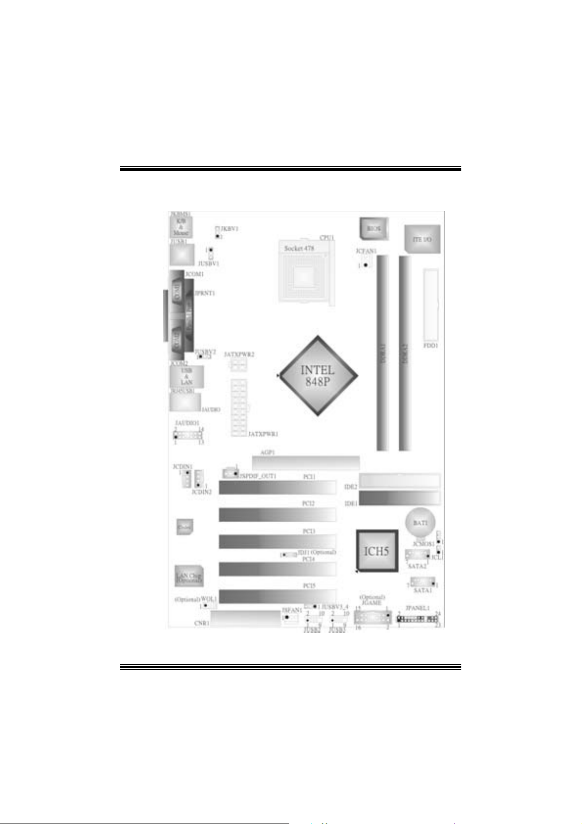
Layout of P4TSP-D2 Version 1.x
NOTE: ●represents the first pin.
1
Page 4
Co mponent Index fo r P4TSP-D2 Versio n 1.x
A. Power Source Selection for Keybo ard and N. Communicatio n Network Riser Slot (CNR1 )
Mouse (JKBV1) O . System FAN H eader (JSFAN1)
B. Power Sour ce Selection for USB P. F ront USB Head er (JUSB2 )
(J USBV1) Q. Front USB Head er (JUSB3)
C. Back Panel Connector R. Power Source Selection for USB
D. Power Source Selection for USB (JUSBV3_4)
(J USB V2) S. Game Port Header (JGAME1): Op tiona l
E. ATX 12V Powe r Connector (JATXPW R2) T. Front Panel Connector (JPANEL1)
F. ATX 12V Po wer Connector (J ATXPW R1) U. Serial ATA Connector (SA TA1-2)
G. Front Audio Head er (JAUDIO1) V. Case Open Connector (JCL1)
H. A cc elera ted Gr aphics Po rt Slot (AGP1) W. Clear C MOS Function (J CMOS1)
I. Digital A udio Connector (JSPDIF_OUT1) X. I DE Connec tors (IDE1-2)
J . CD-ROM Audio-In Header (JCDIN2) Y. DDR DIMM Modul es (DDRA1/ DDRA2)
K. CD-RO M Audio-In Header (JCDI N1) Z. Flopp y Disk Connector (FDD1 )
L. PCI BUS S lots (PCI 1-5) A1. CPU Fan Connector (JCFA N1)
M. W ake On LAN Header (WOL1): Optional B1. Audio DJ Connecto r (JDJ1): O p tional
2
Page 5
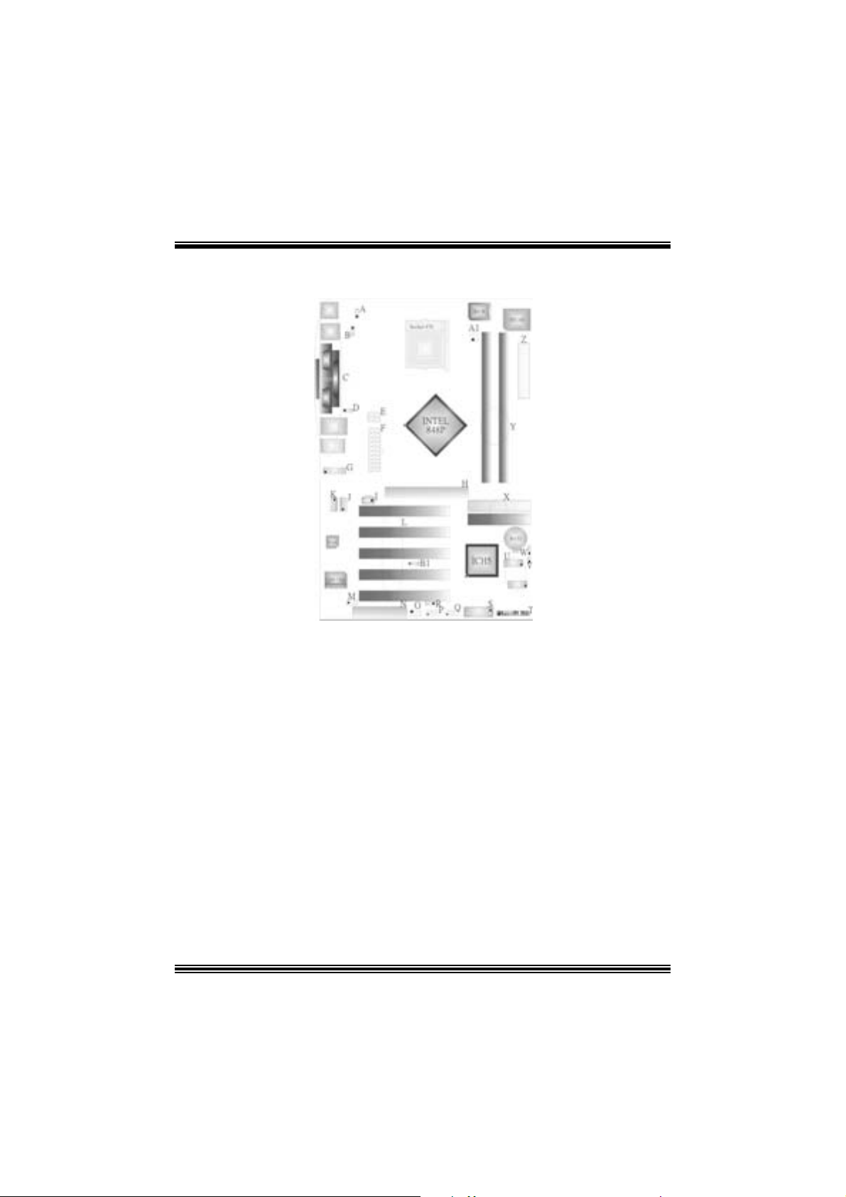
Layout of P4TSP-D2 Versio n 7. x
NOTE: ●represents the first pin.
3
Page 6

English
P4TSP-D 2 Fe a tu r es
A. Har dware
CPU
Prov ides Sock et 478.
Supports the Intel® Pent ium® 4 processor to 3.2GH z.
Supports the Intel® Pent ium® 4 Northwood CPU. (Willamet t e not support ed)
Supports the Intel® Pent ium® 4 478-pin Prescott C PU.
F ront Side Bus at 400/533/800MHz.
Su pports Hyper-Threading Technology.
Chipset
North Bridge: Intel 848P.
South Bridge: Intel ICH 5.
Main Me m o ry
Supports 64-bit wide DDR data channels with 2 DIMMs.
Av ailable bandwidt h up to 3.2GB/s (DDR 400) for single-channel mode.
Supports 128-Mb, 256-Mb, 512-Mb D DR t ec hnologies .
Supports only x8, x16, DDR devices.
Supports four bank devices.
Maxi mu m me mo ry s i ze is 2GB.
Super I/O
Chip: ITE IT 8712.
Low Pin C ount Int erface.
Prov ides the most commonly used legacy Super I/O f unctionality.
Env iro nm ent C ont rol i niti atives ,
- H/W Monitor
- Fan Speed Controller
- I TE's "Smart Guardian" f unction
Slots
F ive 32-bit PCI bus mas t er s lots.
One CNR slot. (only optional on v ersion 1.x )
One AGP 4X/8X compatible slot.
On Board IDE
Supports four IDE di s k dri ves.
Supports PIO Mode 4, Ultra DMA 33/ 66/100 Bus Mas t er Mode.
LAN (optional)
Chip: RTL8 100C/RT L8110S( B)
Support s 10Mb/s, 100Mb/ s, and 1000Mb/s aut o-negotiat ion operation.
4
Page 7

Half / Full duplex capability.
Supports AC PI, PCI power management.
On Bo ard AC’97 Sound Cod ec
Chip: CMI9739A (fo r v.1 .0- v.1.2)/ CM I9761A ( f or v.1 .3 & v.7.x).
Compliant with AC ’97 s pec ificat ion.
AC 97 2. 2 interf ac e (CMI9739A)/ AC97 2.3 interfac e (CMI9761A).
Support s 6 c hannels.
Support s stereo m icrophone. (only f or C MI9761A.)
On Board Periphera ls
a. R e ar sid e
2 s erial port s. (version 7.x only supports one serial port.)
1 parallel port. (SPP/EPP/ECP m ode)
Audio ports in v ert ical posit ion.
1 R J -45 LAN jack. (optional)
PS/2 mouse and PS/2 keyboard.
4 USB2.0 por t s. (optional)
b. Fron t Si d e
1 floppy port supports 2 F DDs with 360K, 720K, 1.2M, 1.44M and 2. 88Mby tes.
4 USB2.0 port s.
1 front audio header.
1 S/PDIF_Ou t header .
Dimensions
ATX F orm Factor: 20.3 X 30.5cm (W x L) (f or v ersion 1. x)
ATX F orm Factor: 20.3 X 29.3 cm (W x L) (for version 7.x )
B. BIOS & S oftware
BIOS
Award legal BI OS.
APM1.2.
ACPI.
USB Function.
Software
Supports Warpspeeder™, 9t h Touch™, BootBlockerTM, W i nFlasherTM, FLASHER™.
Offers the highest performance for Windows 98 SE, Windows 2000, W indows Me,
Windows XP, UNI X series, etc.
P ack age co nt ent s
HDD Cable X 1
FDD Cable X 1
User’s Manual X 1
5
Page 8
Fully Setup Driver CD X 1
USB 2.0 Cable X1 (optional)
S/ PD IF Cable X 1 (optional)
Rear I/ O Panel for ATX Cas e X 1
Serial ATA C able X 1 (optional)
Serial ATA Power Switc h C able X 1 (optional)
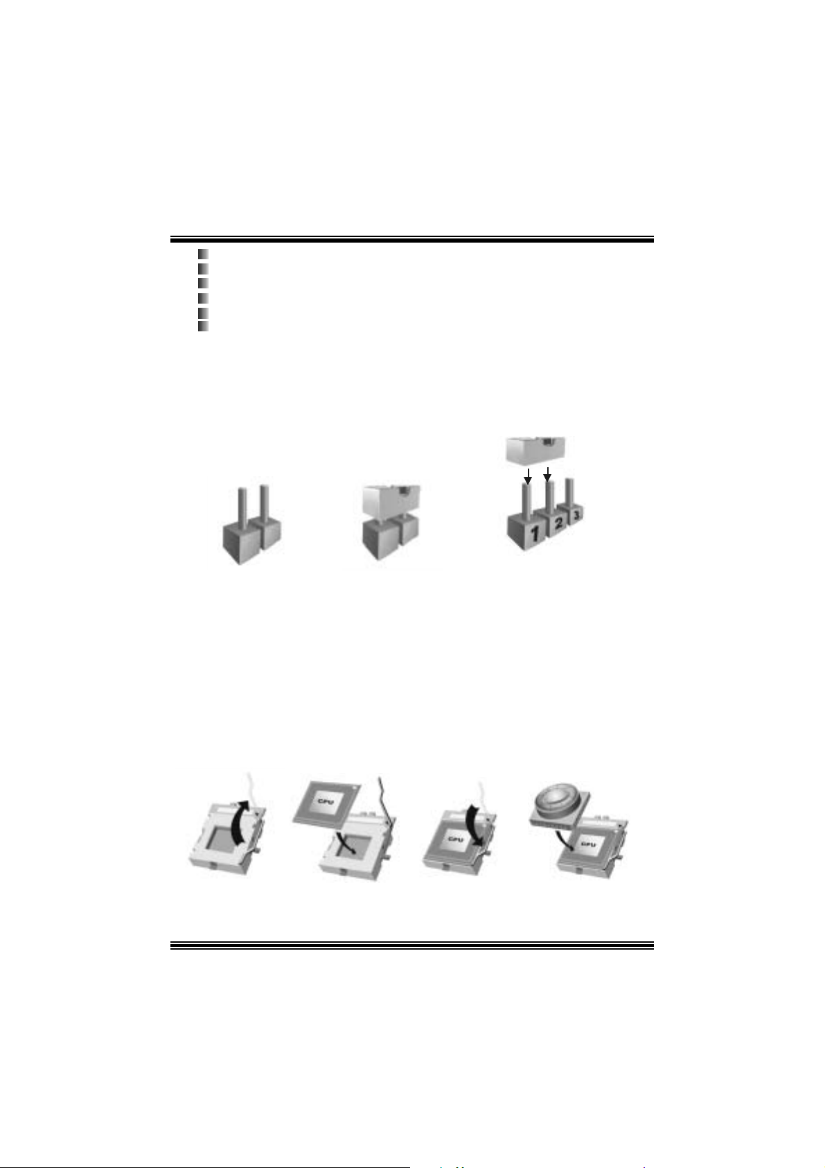
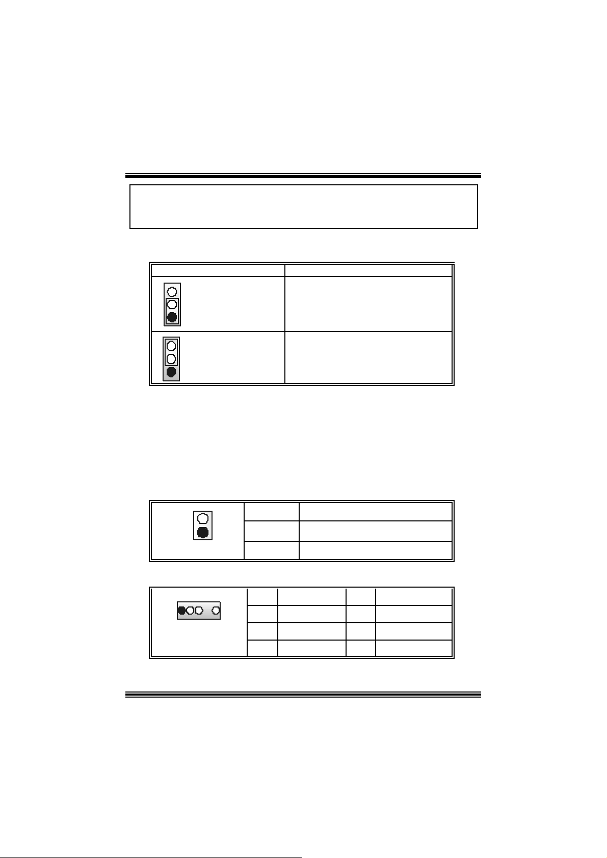
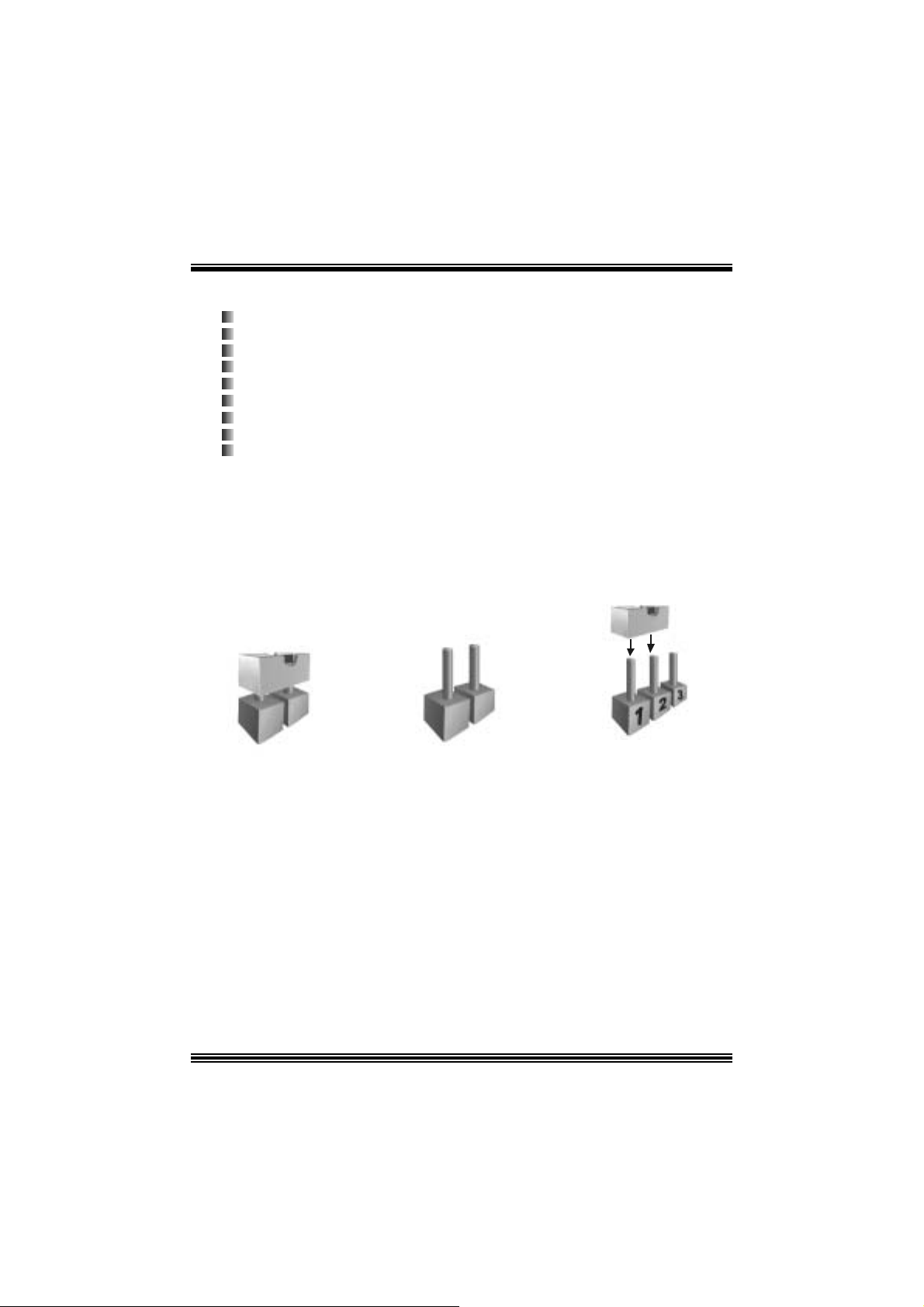
Ho w to set up a Jum pe r?
The illustration s hows how t o s et up jumpers. When a J umper c ap is placed on pins, t he
jumper is “close”. If no jumper cap is placed on the pins, the jumper is ”open”. The
illustration shows a 3-pin jumper whose pin1 and 2 are “close” when a jumper cap is
placed on thes e 2 pins.
Jumper open Jum per close Pin 1-2 close
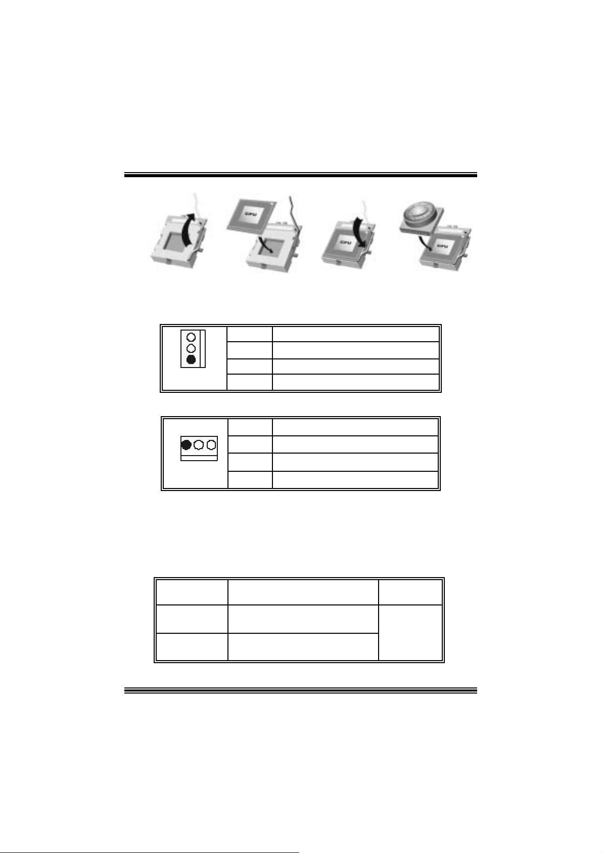
CPU Installation
Step1: Pull the lever sideway s away from the socket and then raise the lev er up to a
90 -degree angl e.
Step2: Look for the whit e dot /cut edge. The whit e dot/ cut edge should point wards the lever
piv ot. The C P U will f it only in the correct orient at ion .
Step3: Hold the CPU down fir mly, an d then cl ose the lever to complete the installation.
Step4: Put the CPU Fan on the C PU and buck le it. Connect the C PU fan power cable to
the JCFAN1. This completes the installation.
Ste p 1 Step2 Step3 Step4
6
Page 9
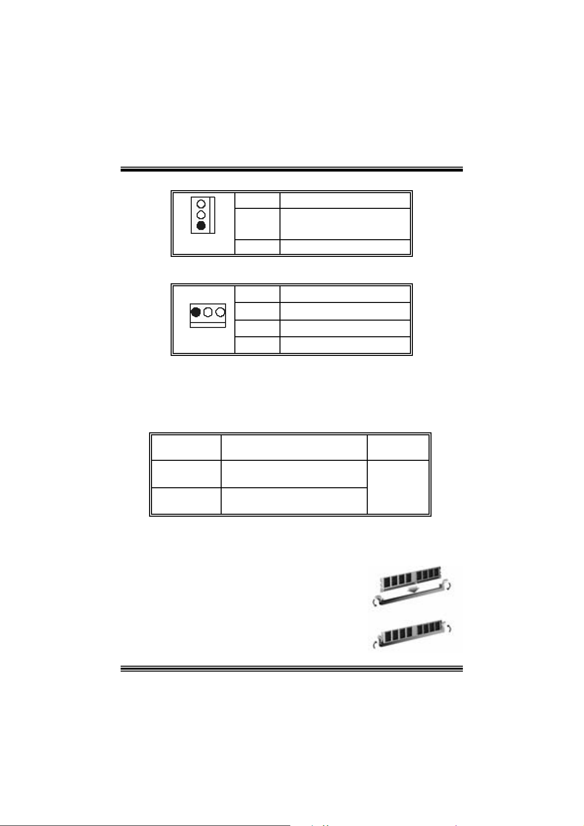
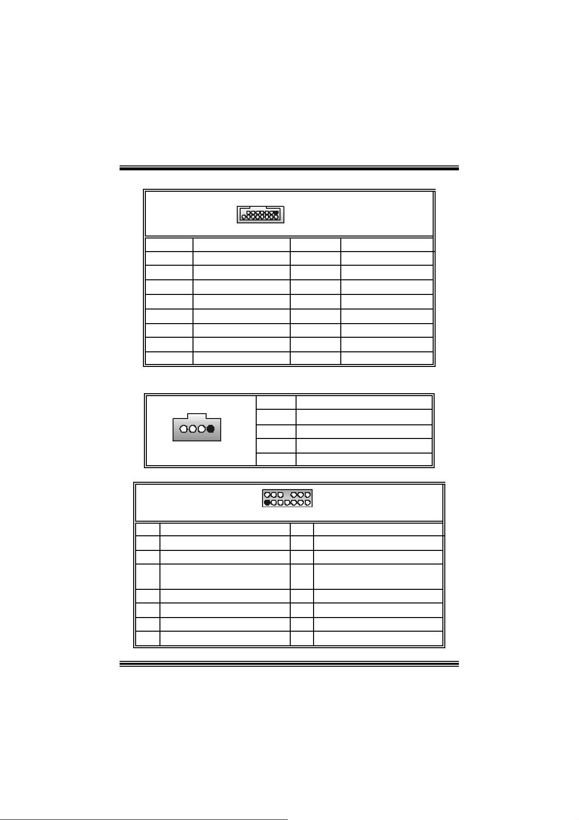
CPU Fan Header: JC FAN1
3
1
JCFAN1
Pin Assignment
1
2
3
Ground
+12V
FAN RPM rate Sense
S ystem Fan Header: JSFAN1
JSFAN1
Pin Assignment
1
31
2
3
FAN RPM rate Sense
Ground
+12V
DDR DI MM Module s: DDRA1/ DDRA2
DRAM Acces s Time: 2.5V Unbuffered/ no regis tered (without ECC) DD R SDRAM
PC2100/ PC 2700/ PC 3200 Type required.
DRAM Ty pe: 128MB/ 256MB/ 512MB/ 1GB DI MM Module. (184 pin)
DIMM Socke t
Location
DDRA1 6 4MB/128MB/256MB/512MB/1GB
DDRA2 6 4MB/128MB/256MB/512MB/1GB
DDR Mod u l e To tal Memory
Size (MB)
*1
*1
***O nly for referenc e***
Max is
2GB
Installing DDR Mod ule
1. U nloc k a DIMM slot by press ing the retaining clips
outward. Align a DIMM to the slot in the way that
the notch of the DIMM mat ches t he break of the
slot.
2. I ns ert the DI MM vertically and firmly into the s lot
until the retaining chip snap back in place and the
DIMM i s properly seated.
7
Page 10
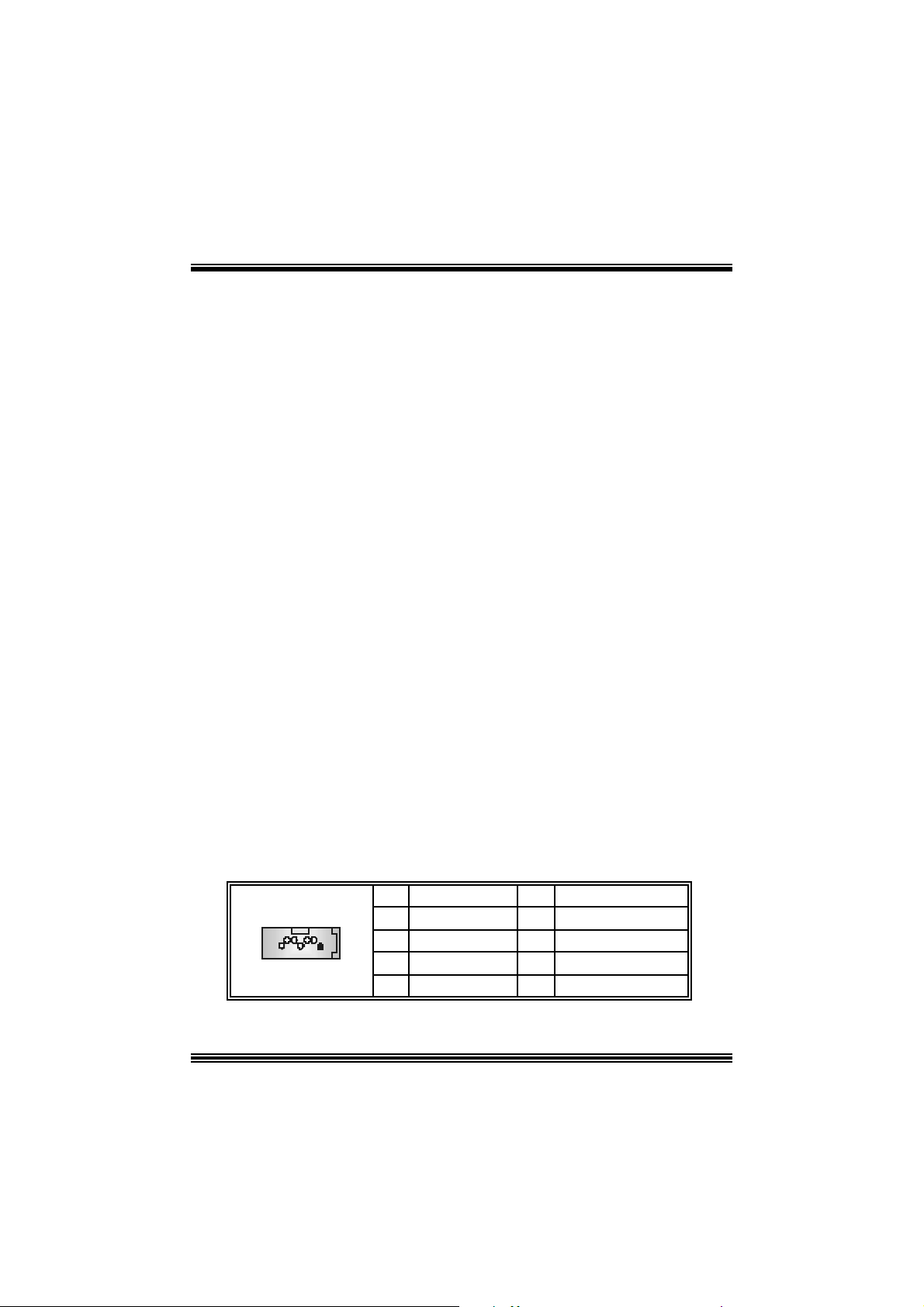
Jump ers, H eade rs , Co nnectors & Slo ts
Floppy Disk Connector: FDD1
The mot herboard provides a standard f loppy disk connector that supports 360K,
720K, 1.2M, 1.44M and 2.88M floppy disk types. This connector supports the
prov ided f loppy drive ribbon cables .
Hard Disk Connectors: IDE1/ IDE2
The motherboard has a 32-bit Enhanced PCI IDE Controller that provides PIO
Mode 0~4, Bus Mast er, and U ltra DMA 33/ 66/ 100 f unctionality. I t has two H DD
connectors ID E1 (primary) and IDE2 (secondary).
The ID E c onnectors can c onnect a master and a slav e driv e, so y ou can c onnect
up to four hard disk drives . The f irst hard drive s hould alway s be c onnected t o
IDE1.
Peripheral Component Interconnect Slots: PCI 1-5
This m ot herboard is equipped with 5 st andard PCI s lots. PCI stands for Peripheral
Component I nterconnec t, and it is a bus standard for expansion cards. This PCI
slot is des ignated as 32 bits.
Accelerate d Graphics Port Slot: AGP1
Your monitor will attach directly to that video card. This motherboard supports
video cards f or PC I s lots, but it is als o equipped with an Accelerated Graphics Port
(AGP). An AGP c ard will take advantage of AGP technology f or improv ed video
efficiency and perform ance, es pecially with 3D graphics.
Communication Network Riser Slot: CNR1 (not su pport version
7.x)
The CNR specification is an open I ndust ry St andard Architecture, and it def ines a
ha rdw ar e scalable r iser card interfa ce, which su pports modem only.
S erial ATA C onnecto r: SATA1/ SAT A2
The mot herboard has a PCI to SATA C ontroller with 2 channels SATA interface, it
satisfi es t he SA T A 1. 0 s pec and wit h t r an s fer rat e of 1. 5Gb/s .
1234567
SATA1/ SATA2
Pin Assignment Pin Assignment
1
3
5
7
Ground
TXRX-
Ground
2
4
6
TX+
Ground
RX+
8
Page 11
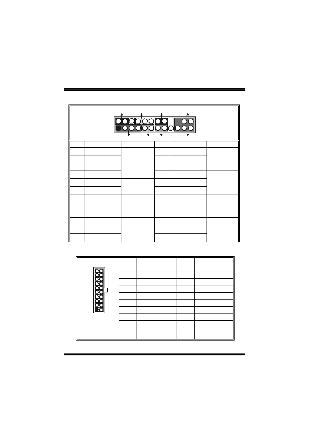
Front Pane l Conne ctor: JPANEL1
SLP
JPANEL1
2
123
Pin Assignment Function Pin Assignment Function
1 +5V 2 Sleep Control
3 NA 4 Ground
5 NA 6 NA NA
7 Speaker
9 HD D LED (+ ) 10 Powe r LED (+)
11 HDD LED (-)
13 Ground 14 Power Butt on
15 Reset Control
17 NA 18 KEY
19 NA 20 KEY
21 +5V 22 Ground
23 IRTX
PWR_LED
(+) (-)(+)
SPK
Connector
Hard Drive
Connector
(+) (-)
HLED
RST
Speaker
8 Power LED (+)
LED 12 Power LED (-)
Reset
Button 16 Ground
IrDA
24 IRR X
IRON/ OFF
IR
24
Sleep
Button
POWER
LED
Power-on
Button
IrDA
Connector
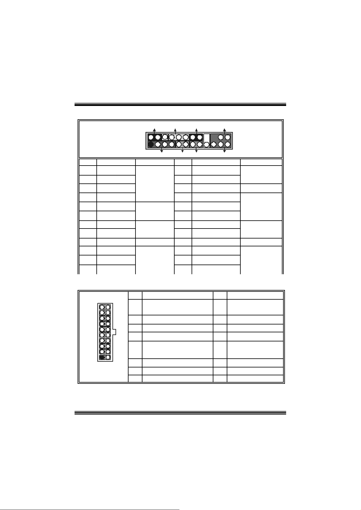
Power Conn ectors: JATXPWR1/ JATXPWR2
10
1
JATXPWR1
20
11
PIN Assignment PIN Assignment
1
2
3
4
5
6
7
8
9
10
+3.3V
+3.3V
Ground
+5 V
Ground
+5 V
Ground
PW_OK
Standby Volt age
+5 V
+1 2V
9
11
12
13
14
15
16
17
18
19
20
+3. 3V
-12V
Ground
PS_ON
Ground
Ground
Ground
-5V
+5V
+5V
Page 12
1
1
3
2
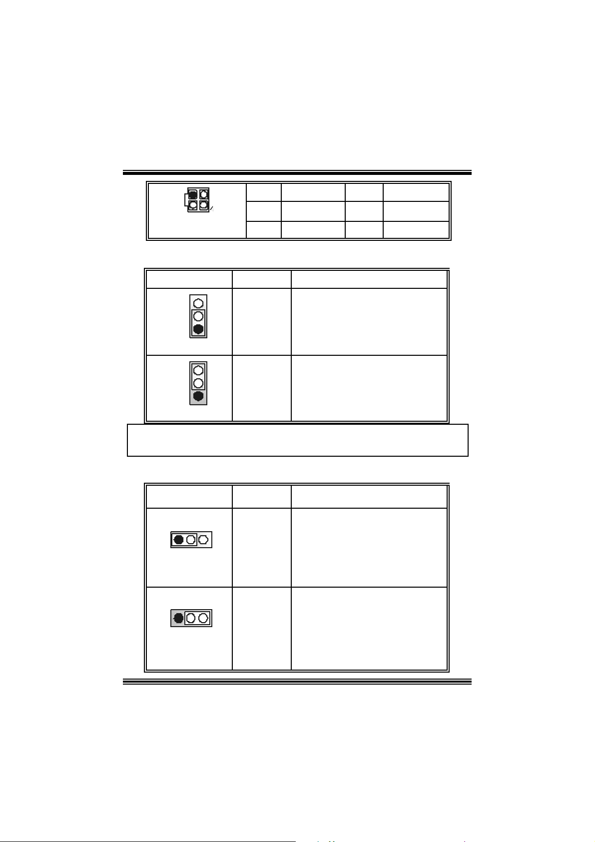
JATXPWR2
PIN Assignment PIN Assignment
1
2
+12V
+12V
3
4
Ground
Ground
Power Source Selection for Keyboard/ Mouse: JKBV1 (only
optional on version 1.x)
JKBV1 Assignment Description
3
1
Pin 1-2 c los e
3
1
Pin 2-3 c los e
+5 V
+5V Standby
Voltage
+5V for keybo ard and mouse
PS/2 Mous e and PS/2 Key board are
powered with +5V standby v oltage
No t e: In o rder to su pport th i s fun cti o n “Pow e r-o n sy ste m v i a ke yb oa rd and
mouse”, “JKBV1” jumper cap should be placed on pin 2-3.
Power Source Selection for USB: JUSBV1/ JUSBV2/ JUSBV3_4
(only optional on version 1.x)
JUSBV1/JUSBV2/
JUSBV3_4
1 3
Pin 1-2 c los e
1 3
Pin 2-3 c los e
Assignment Description
+5 V
+5V Standby
Voltage
JUSBV1 : 5V for USB at th e JUSB1
connector port
JUSBV2: 5V f or USB at t he JRJ 45USB
coonector port
JUSBV3_4 : 5V for USB at the JUSB2/3
JU SBV1: JUSB1 port powered with
JU SBV2: JRJ 45USB1 port powered
JU SBV3_4: JUSB2/3 ports powered
10
connector ports
standby v olt age of 5V
with s t andby v olt age of 5V
with s t andby v olt age of 5V
Page 13
Note: In order to support thi s function “Power-on system via USB devi ce”,
“JUSBV1/JUSBV2/ JUSBV3_4” jumper cap should be placed on pin 2-3
individually.
Clear CMOS Jumper: JCMOS1
JCMOS1 Assignment
3
1
3
1
Pi n 1-2 C lose
Pi n 2-3 C lose
Norm al Operation (def ault)
Clear CMOS Data
※ Clear CMOS Procedures:
1. R emov e AC power line.
2. Set the jumper to “Pin 2-3 C lose”.
3. Wa it for fi ve seconds.
4. Set the jumper to “Pin 1-2 C lose”.
5. Power on t he AC .
6. R eset your des ired password or clear t he C MOS dat a.
Ca se Op e n Connec to r: JCL1
Pin
1
JCL1
1
2
Assignment
Cas e Open Signal
Ground
AUDIO DJ Connector: JDJ1 (only optional on version 1.x)
15
JDJ1
Pin Assignment Pin Assignment
SMBDATA
1
3
5
INT_B
ATX_PWROK
2
4
SMBCLK
KEY
11
Page 14
X
t
Game Header: JGAME1 (only optional on version 1.x)
15
Pin Assign m ent Pin Assignment
1
3
5
7
9
11
13
15
Joy stick B C oordinate X
Joy stick B C oordinate Y
+5V
Joy stick B Butt on 1
MIDI Output
Joy stick B Butt on 2
MIDI Input
NA
1
216
JGAME1
2
4
6
8
10
12
14
16
+5V
Joystick A Button 1
Joy st ick A Coordinate
Ground
Ground
Joy st ick A Coordinate Y
Joystick A Button 2
+5V
CD-ROM Audio-In Heade r: JCDIN1/ (JCDIN2: only optional
on version 1.x)
1
JCDIN1/ JCDIN2
Pin Assignment
1
2
3
4
Left Channel Inpu t
Ground
Ground
Right Channel Inp ut
Front Panel Audio Header: JAUDIO1
2
1
JAUDIO1
Pin Assignment Pin Assign m ent
1
3
5
7
Left Line Out/ Speaker Out Left
9
Right Line I n/ R ear Speaker R ight
11
Left Line In/ Rear Speaker Left
13
Mic In / C e nte r
Mic Power/ Bass
Right Line Out/ Speak er Out
Right
Reserv ed
12
14
13
2
4
Right Line Out/ Speaker Out Righ
6
8
Left Line Out/ Speaker Out Left
10
Right Line In/ R ear Speaker Right
12
Lef t Line I n/ Rear Speaker Left
14
Ground
Audio Power
Key
Page 15
Digital Audio Connector: JSPDIF_OUT1 (optional )
1
JSPDI F_OUT1
Pin Assignment
1
2
3
+5V
SPDIF_OUT
Ground
Wake On LAN He ade r: WOL1 (only optional on version 1.x)
1
WOL1
Pin Assignment
1 +5V_Standby
2
3 Wake up
Ground
Front USB Header: JUSB2/JUSB3
9
10
JUSB2/3
Pin Assignment Pin Assignment
1
1
3
2
5
7
9
+5V
USB-
USB+
Ground
KEY
2
4
6
8
10
+5 V
USB-
USB+
Ground
NA
Auxiliary Audio-In C onnector: JAUX1 (only optional on version
7.x)
1
JAUX1
Pin Assignment
1
2
3
4
Left channel AUX_IN
CD_Ground
CD_Ground
Righ c hannel AUX_I N
S M Bus Cons ume r In frared Header: JS MB_C IR (onl y opti onal
on version 7.x)
8
7
12
JSMB_CI R
Pin Assignment Pin Assignment
1
3
5
7
Ground
CIRRX
NA
SMBDATA
13
2
4
6
8
+5V St andby
CIRTX
Power-on Butt on
SMBCLK
Page 16
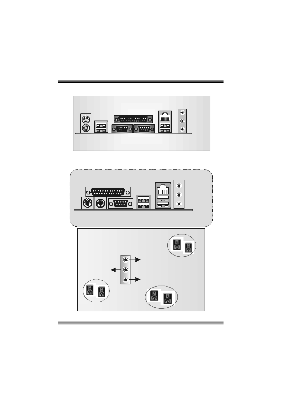
Back Pa nel Co nnectors (for version 1.x)
JKBMS1
PS/2
Mouse
PS/2
Keyboard
JUSB1
USB
Parallel Port
COM1
JCOM1
JPRNT1
JCOM2
JRJ45USB1
LAN
(optional)
COM2 USB
B ack Panel Connectors (for version 7.x)
Line In
Speaker Out
MIC In
JAUDIO
Pri nter Port
PS/2
Keyboard
PS / 2
Mouse
6 Channe l Speake rs
Speaker Out/
Right & Le ft
COM1
LAN
U SB
USB
(Optional)
Li n e In /
Rear Spea ker (Le ft & Right)
Mic In/ Center & Bass
Line In
Speak e r Out
Mic In
14
Page 17

Deutsch
Die Spezifikationen von P4TSP-D2
A. Har dware
CPU
U terstüt zung für Sock el 478.
U nterstützung f ür Int el CPU Nort hwood. (Willamette wird nicht unterg es t ützt)
Unterstützung für den Intel Pentium® 4 Prozessor bis zu 3.2GH z.
Unterstützung für den Intel Pentium® 4 P r esc o t t C P U.
F SB mit 400/ 533/ 800MHz.
Uterstützung für die H yper-T hreading Technolo gi e.
Chipsatz
D ie Northbridge: Intel 848P.
D ie Southbridge: Intel ICH 5.
Hauptspeicher
U nterstüt zung für 64-bit Breite D DR-Dat enk anal mit ein oder zwei DIMMs pro
Kanal.
Verf ügbare Bandbreite bis zu 3. 2GB/s (DD R400) f ür Einzeln-Kanal-Modus.
U nterstüt zung für 128-MB, 256-Mb und 512-Mb DDR Tec hnologie.
Unt e r st ü t zung f ü r x8, x1 6 DDR Ger ä t e.
Vier DDR Speicherbänk e.
D ie m ax imale Speichergröße ist 2GB.
Super I/O
Chip: ITE IT 8712.
Low Pin C ount Int erface.
D ie m eisten gemeinsam en vergebraucht en Super I/ O Funktionen werden gelief ert.
Umweltkontroll-Initiative:
- H/W Monitor
- Vetilator-Geschwindigkeit-Controller
- I TE's "Smart Guardian" Funkt ion
Steckplätze
F ünf 32-bit PCI-Bus-Slots.
Ein C NR-Slot. (optional)
Ein 4X/ 8X AGP-Slot.
Onboard-IDE
Unterstützung fü r vi er IDE Diskettenl au fwe rke.
U nterstüt zung für PIO Modus 4, Ult ra DMA 33/ 66/100 Bus Master Modus.
LAN (optional)
15
Page 18

Chip: RTL8 100C/ RTL8110S (B).
U nterstüt zung für 10 Mb/s, 100 Mb/ s und 1000Mb/s Auto-Negot iation.
Halb/Voll-Duple x Fä higkei t.
U nterstüt zung für ACPI, PCI Power Managem ent.
Onboard AC’97 Sound Codec
Chip: C MI9739A (für v ers ion 1. 0-12)/CMI 9761A (für v ersion 1.3 & v ersion 7.x ).
Ent s pricht der Spezif ikation von AC ’97.
AC 97 2. 2 Interf ace (CMI9739A)/ AC 97 2.3 Interf ace (CMI9761A).
Unterstützung für 6-Kanal.
Unterstützung für Stereo-Mikrof on (für CMI9761A).
Onboar d-Periph eriegeräte
a. R ü c kwan d
2 s erielle Sc hnittstellen. (1 s erielle Schnittstelle für version 7.x)
1 parallele Sc hnittstelle. (SPP/EPP/ECP-Modus )
Audio-Sc hnittst ellen auf der v ertikalen Posit ion.
1 R J -45 LAN Buc hse.(optional)
PS/ 2-Maus und PS/2-Tastatur.
4 USB2.0-Ports.
b. Vorder seit e
1 F loppy-Port m it Unterstützung f ür 2 Dis k et t enlauf werke.(360KB, 720KB, 1.2MB,
1.44MB und 2.88MB)
4 USB 2.0- P or ts .
1 Front- Audio-Head er.
1 S/PDIF-Header. (o ptional)
Abmessung
ATX F orm -Fac tor: 20.3 X 30.5c m (W X L)
ATX F orm -Fac tor: 20.3 X 30.5c m (W X L) (f ür v ersion 7. x)
B. BIOS & S oftware
BIOS
Award legal BI OS.
Unterstützung für APM1. 2.
Unterstützung ACPI.
Unterstütz ung USB Funkion.
Software
Unterstützung für Wa rps peede r ™, 9 th T ouch™, BootBlockerTM, WinFl as herTM,
FLASHER™
Unter stützung für die am meis ten ver breite ten Betriebsyst e me wi e Win d ows
98SE. , Windows 2000, Windows ME, Windows XP and SCO UNIX us w..
16
Page 19
Verpack ungsinhalt
HDD Kable X 1
FDD Kable X 1
Benut zer Handbuch X1
Treiber C D für Installation X1
USB 2.0 Kable X1 (opt ional)
S/ PD IF Kable X 1 (optional)
I/O-R üc k wand für ATX Gehäuse X 1
Serial ATA Kable X 1 (opt ional)
Serial ATA N et zsc halter Kable X 1 (optional)
Ei nst e l lu ng de r Jum per
Die Abbildung verdeutlicht, wie Jumper eingestellt werden. Pins werden durch die
Jum per-Kappe v erdeckt, ist der Jum per ”geschlossen”. Keine Pins werden durch die
Jum per-Kappe verdeckt, is t der Jum per “geöffnet”. Die Abbiildung zeigt einen 3-Pin
Jumper dessen Pin1 und Pin2 ”geschlossen“ sind, bzw. es bef indet sich eine
Jum per-Kappe auf dies en beiden Pins.
Jumper geschlossen Jumper geöffnet Pin1-2 geschlossen
In stallat ion der CPU
Sc hritt 1 : Z iehen Sie den H ebel s eitlich vom Sockel weg. Heben Sie den Hebel dann
in 90-Grad-Winkel nac h oben.
Sc hritt 2 : Suchen Sie nac h der scharfen Kant e, die auf D rehpunkt des Hebels
weisen m uss . Die CPU passt nur, wenn s ie ric htig aus geric ht et ist.
Sc hritt 3 : D rück en Sie die CPU f est in den Sock el und s c hließ en Sie den Hebel.
Sc hritt 4 : St eck en S ie Ihr en C PU -Lüf t er auf die C PU . Schli eße n Sie die
Strom verso rgungsstecker für CPU-Lüfter an JCFAN1 an . Dann be enden
Sie die I nstallation.
17
Page 20
Schritt 1 Schritt 2 Schritt 3 Schritt 4
CPU- Lüfter Header: JCFAN1
3
1
JCFAN1
Pin Beschreibung
1
2
3
Lüft er R PM Geschwindigk eit Sens or
Masse
+12V
System-Lüfter Header: JSFAN1
JSFAN1
Pin Beschreibung
1
31
2
3
Lüft er R PM Geschwindigk eit Sens or
Masse
+12V
DDR- DIMM-Mo dule s: DDRA1/ DDRA2
DRAM-Zugriffs zeit: 2.5V unbuf f ered/ nicht regist rierter (ohne EC C) DDR SDR AM
PC2100/ PC 2700/ PC 3200 Ty p erforderlich.
DRAM-Ty p: 128MB/ 256MB/ 512MB/ 1GB D I MM-Module (184-Pin)
DIMM-Sockel
Standort
DDRA1
DDRA2
64MB/128MB/256MB/512 MB/1G B
64MB/128MB/256MB/512 MB/1G B
DDR-Module Speichergröße
(MB)
*1
*1
***Nur als Referenz***
Ma ximal ist
2GB
18
Page 21

In stallat ion von DDR-Modul
1. Öffnen Sie einen DIMM-Slots, indem Sie die
seitlich Chips nach außen drücken. Richten Sie
da s DIMM-Mo dul so über dem Slot aus , dass das
Modul mit der Kerbe in den Slot pas st.
2. D rücken Sie das DI MM-Modul in den Slot, bis die
seitlichen Clips zus chnappen und das Modul fes t
sitzt.
Jump ers, H eade rs, Anschlüs s e & S lot s
Diskettenanschluss: FDD1
Das Motherboard enthält einen st andardmäßigen Diskettenans chluss, der 360K-,
720K-, 1.2M-, 1.44M- und 2.88M-Disketten unterstützt. Dieser Anschluss
unt ers tützt die mit gelief erte Bandkabel des Diskettenlauf werks.
Fe stplatt enanschlüsse: IDE1 und ID E2
Das Mainboard hat einen 32-Bit Enhanced PCI IDE-Controller, der die Modi
PIO0~4, Bus Mast er sowie die U ltra DMA/33/ 66/100/133- Funkt ion zur Verfügung
stellt. Dieser ist mit zweii HDD-Anschlüssen versehen IDE1 (primär) und IDE2
(sekundär).
Die ID E-Anschlüsse k önnen eine Master- und eine Slav e-Festplatte v erbinden, so
dass bis zu 4 Festplatten angeschlossen werden können. Die erste Festplatte
sollte im m er an IDE1 angeschlossen werden.
Peripheral Component Interconnect Slots: PCI 1-5
Dieses Motherboard ist m it 5 standardmäß igen PCI-Slots ausgestattet. PC I steht
für Peripheral Component Interc onnect und bezieht sich auf einem Busst andard für
Erweiterungskarten, der den älteren ISA-Busstandard in den meisten
Schnittst ellen ers etzt hat. Dieser PCI-Slot ist f ür 32 bits v orgesehen.
Accelerate d Graphics Port Slot: AGP1
Ihr Monitor wird direkt an die Grafikkarte angeschlossen. Dieses Motherboard
unterstützt Grafikkarten f ür PCI-Slots, aber es ist auch mit einem Accelerated
Graphic s Port ausges tattet. AGP-Karten v erwenden die AGP-Technologie, um die
Wirks amk eit und Leistung v on Videosignalen zu v erbessern, besonders wenn es
sich um 3D-Graf iken handelt.
Commun ication Netwo rk Rise r Slot: CNR1 (op tiona l)
Die CNR-Angaben entsprechen einer off enen I ndustry Standard Archit ecture, und sie
definieren eine Hardware-skalierbare Riser-Card-Schnittstelle, welche nur Audio,
Netzwerk und Modem unterstützt.
Serial ATA Co nnector: JSATA1/JSATA2
Auf dies en Motherboard gibt es ein PCI -to-SATA C ont roller m it 2-Kanal Interfac e,
die der Spezifikation von SATA 1.0 ent spricht ( D t enübert ragung m it 1.5Gb/S)
19
Page 22
Anschlüsse für die Vo rderseite: J PANEL1
PWR_LED
SLP
(+) (-)(+)
JPANEL 1
Pin Belegung Funktion Pin Belegung Funktion
1 +5V 2 Schlaf- Kont roll
3 Kein 4 Erde
5 Kein 6 Kein Kein
7 Lautsprecher
9 HDD LED (+) 10 P ower LED (+)
11 HDD LED (-)
13
15
17 Kein 18 Schlüsse
19
21
23
Masse
Re set-Kontroll
Kein
+5V
IRTX
224
123
(+) (-)
SPK
Lautsprecher-
Anschluss
Festplatte
LED 12 Power LED (-)
Rückstell-
knopf
IrDA-
Anschluss
HLED
RST
8 Power LED (+)
14
16 Erde
20
22 Erde
24
Power-Knopf
Schlüsse
IRR X
IRON/OFF
IR
Schlaf-
Knopf
POWER
LED
Power-On
Knopf
IrDA
Anschluss
Power Conn ectors: JATXPWR1/ JATXPWR2
10
1
JATXPW R1
PIN Belegung PIN Belegung
20
11
1
2
3 Erde 13
4
5 Erde 15 Erd e
6
7 Erde 17 Erd e
8
+5V reserv ierte Spannung
9
10
+3.3V
+3.3V
+5V
+5V
PW_OK
+12V
11
12
14
16 Erd e
18
19
20
+3.3V
-12V
Masse
PS_ON
-5V
+5V
+5V
20
Page 23

1
3
2
JATXPWR2
PIN Belegung PIN Belegung
1
2
+12V
+12V
3 Erde
4
Erde
Auswahl von S tromsmodi für Tastatur/ Maus: JKBV1 (optional)
JKBV1 Pin-Belegung Beschreibung
3
1
Pin 1-2 gesc hlossen
3
1
Pin 2-3 geschlossen
+5V +5V f ür Tastatur und Maus
+ 5V re s erv i ert e
Spannung
Durch +5V reserviert e Spannung für
PS/2-Maus und PS/ 2-Tas t at ur zum
Erwecken vo m System
Anmerkung: Um die Funktion ―“Erwecken durch Tastatur/Maus“ ― zu
aktivieren, müssen Pins 2-3 von JKBV1 durch die Jumperkappe verdeckt
werden.
Auswahl von Stromsmodi fü r USB: JUSBV1/ JUSBV2/
JUSBV3_4 (optional)
JUSBV1/JUSBV2/
JUSBV3_4
1 3
Pin 1-2 gesc hlossen
1 3
Pin 2-3 gesch lossen
Pin-Belegung Beschreibung
JUSB V1: 5V fü r USB-Port von JU SB1
JUSB V2: 5V fü r USB-Port von
+5V
+ 5V r es erv i ert e
Spannung
JRJ45USB1
JUSB V3_4: 5V für USB-Por t von
JUSB2/3
JU SBV1: 5V reservierte Spannung f ür
JU SB1 zum Erweck en
JU SBV2: 5V reservierte Spannung f ür
JRJ45USB1 zum Erwecken
JUSBV3_4: 5V reserv iert e Spannung
für JUSB2/3 zum Erweck en
21
Page 24

Anmerkung: Um die Funktion ―“Erwecken durch USB-Geräte“―zu
aktivieren, müssen Pins 2-3 von “JUSBV1/JUSBV2/ JUSBV3_4”durch
die Jump erkappe ver deckt werden.
Jumper zum Löschen des CMOS: JCMOS1
3
1
3
1
JCMOS1 Beschreibung
Norm ale Operation (D ef ault)
Pin 1-2 geschloss en
CMOS-Dat en zum Löschen
Pin 2-3 geschloss en
※ Prozed u r en z u m Lö sc h en d e s CMOS :
1. Aussc halten Sie das Syst em.
2. Lassen Sie Pin 2-3 von JC OMS1 ges hclossen sein.
3. Bitte wart en Sie 15 Sekunden.
4. Lassen Sie Pin 1-2 von JC OMS1 ges hclossen sein.
5. Einschalten Sie das System wieder.
6. Zurücksetzen Sie ihr gewunschtes Kennwort oder löschen Sie die
CMOS-Daten.
Serial ATA Anschlüsse: S ATA1/ SATA2
1234567
SATA1/ SATA2
Pin Belegung Pin Belegung
1
3
5
7
Erde
TXRX-
Erde
2
4
6
TX+
Erde
RX+
Warnmeldung für Chassis-Öffnen Anschluss: JCL1
Belegung
Erde
1
JCL1
Pin
1
2
Warnmel dung fü r Chassis-Öffnen
22
Page 25

AUD IO DJ Anschluss: JDJ1 (opt ional)
15
JDJ1
Pin Belegung Pin Belegung
SMBDATA
1
3
5
INT_B
ATX_PWROK
2
4
SMBCLK
Schlüsse
Game Header: JGAME1 (option al)
15
Pin Belegung Pin Belegung
1
3
5
7
9
11 J oy st ic k B Knopf 2 12 Joy stick A Koordierung Y
13
15
Joy stick B Koordierung X
Joystick B Koordierung Y
+5V
Joy stick B Knopf 1
MIDI Aus gabe
MIDI Eingabe
Kein
1
216
JGAME1
2
4
6
8
10
14
16
+5V
Joystick A Knopf 1
Joy stick A Koordierung X
Erde
Erde
Joystick A Knopf 2
+5V
CD-ROM Audio-In Heade r: JCDIN1/ (JCDIN2: optional)
1
JCDIN1/ JCDIN2
Pin Belegung
1
2
3
4
Linkk anal Eingabe
Erde
Erde
Rec htkanal Eingabe
Digital Audio Anschluss: JSPDIF_OUT1 (optional)
JSPDI F_OUT1
Pi n B elegu ng
1
1
2
3
23
+5V
SPDIF_Ausgabe
Erde
Page 26

n
r
Front Panel Audio Header: JAUDIO1
2
1
JAUDIO1
Pin Belegung Pi n Belegung
1
3
5
7
9
11
13
Mikrofon-Eingang/
Zentrum
Mikrofon-Betriebsspannung
/Bass
Audio-Signal des rechten
Kanals zur Vorderseite /
Lauts precher-Signal des rec ht e
Kanals zur Vorderseite
Reservieret für spät.
Verwendung durc h
Kopf hörer-Verstärker
Audio-Signal des linken Kanals
zur Vorderseite /
Lauts precher-Signal des linken
Kanals zur Vorderseite
Audio-Signal des rechten
Kanals von der Vorders eite /
Lauts precher-Signal des rec ht en
Kanals von der Vorderseite
Audio-Signal des linken Kanals
von der Vorderseite/
Lauts precher-Signal des linken
Kanals von der Vorderseite
14
13
2
4
6
8
10
12
14
Audio-Bet riebss pannung
Audio-Signal des rechten Kanals zu
Vord er seite / Lau tsprecher-Signal
des recht en Kanals zur Vorderseite
Audio-Signal des linken Kanals zur
Vord er seite / Lau tsprecher-Signal
des linken Kanals zur Vorderseite
Audio-Signal des recht en Kanals
von der Vorderseite/
Laut s prec her-Signal des recht en
Kanals v on der Vorderseit e
Audio-Signal des linken Kanals von
Lau tspreche r-Si gnal des linke n
Kanals v on der Vorderseit e
Erde
Schlüsse
der Vorders eite/
Wake On LAN Header: WOL1 (optional)
1
WOL1
Pin
1 +5V_SB
2
3 Wake-up
24
Beschreibung
Erde
Page 27

7
Front USB Header: JUSB2/JUSB3
9
10
JUSB2/3
Pin Belegung Pin Belegung
+5V(geschm elzt)
1
1
3 USB- 4 USB-
2
5
7 Erde 8 Erde
9
USB+
Schlüsse
Auxiliary Audio-In C onnector: JAUX1 (optional)
+5V(geschmelzt)
2
6
10
USB+
Kein
1
JAUX1
Pin Assignment
1
2
3
4 Righ c hannel AUX_IN
Left channel AUX_IN
CD_Erde
CD_Erde
S M Bus Consumer Infrared Header: JSMB_CIR (optional)
8
12
JSMB_CI R
Pin Assignment Pin Assignment
1 Erde 2
3
5
7
CIRRX
Kein
SMBDATA
+5V geschmelzt
4
Power-on Butt on
6
8
SMBCLK
Anschlüsse für die Rückwand
CIRTX
25
Page 28

Anschlüsse für die Rückwand (für version 7.x)
Printer Port
PS/2
Keyboard
PS / 2
Mouse
6 Kanal Lautsprecher
Lautsprecher Ausgang/
Fornt-Lautsprecher
(L/R)
COM1
LAN
USB
USB
(Optional)
Line-In/ R cklautspreche r
(L/ R)
Zent rallautsprecher & Bass
ü
Mik rofon Eingang/
Line In
Speak er Out
Mic In
26
Page 29

Français
Caractéristiques de P4TSP-D2
CPU
Off re les Sock et-478.
Support e le proc esseur I nt el Pent ium 4 jusqu’à 3.2GHz.
Support e I ntel Pentium 4 N ort hwood CPU . ( Willamet te not support ed)
Support e I nt el Pentium 4 478 Prescott CPU.
Fonctionnant en Bus Frontal de 400/ 533/800MH z.
Supporte Hyper-Threading. (seulm ent pour onboard VGA)
Chipset
North Bridge: Int el 848P
South Bridge: Intel ICH5
Mémoire Principale
Prend en c harge un ou deux canaux de données DD R de 64 bits de large
avec 1 DIMM par canal.
Bande pas s ant disponible jus qu’à 3.2Go/s (DDR 400) pour le m ode canal
sim ple et 6.4Go/s (DDR 400) pour m ode canal double.
Prend en c harge les technologies DD R 128 Mo, 256 Mo, 512 Mo.
Prend en c harge s eulement les périphériques DDR x8, x 1 6. (N e pr end p as
en charge les D I MM et ECC en registres)
Prend en c harge quat re banques de m émoire.
La t aille max im um de la mémoire est de 2Go.
Super E/S
Puce: ITE IT8712.
Int erf ace de Com pt age de Broche F aible.
Off re la f onctionnalit é Super E/ S héritée la plus couramment ut ilis ée.
Initiatives de Contrôle d’Environnement,
- Moniteur H/ W
- Fonct ion "Sm art Guardian" de ITE
Slots
5 slots de maît rise de bus PCI 32 bits.
Un slot C NR. (optionnel)
Un slot AGP 4X/8X.
IDE Interne
Support e quatre disques durs IDE.
Support e PI O Mode 4, le Mode Maît re et le Mode de Maît rise de Bus Ultra
DMA 33/ 66/ 100/133.
LAN (optionnel)
RealTek RTL8100C/RTL8110S(B).
Support e N égoc iat ion aut omatique : 10/100/ 1000 Mb/s.
Full/Half Duplex.
Support e ACPI , PCI Power managem ent.
Codec Son AC ’ 97 In tern e
CMI9739A (pour v ers ion 1.0-1. 2)/CMI9761A (pour v ersion 1.3 & 7.x)
27
Page 30

Conforme aux spéc ifications du codec AC’97.
Supporte 6 canaux.
Prend en c harge le mic rophone stéréo. (pour C MI9761A)
Périphériques Internes
a. Côté arrière
2 port s série (1 port pour v ersion 7.x )
1 port parallèle (mode SPP/EPP/E CP)
Ports audio en pos it ion v erticale.
1 port RJ -45 LAN. (Opt ionnel)
S ou ri s PS / 2 et cl av ier PS/ 2.
4 port s USB2.0.
b. Côté frontal :
1 port disquett e prenant en charge 2 FDD avec 360K, 720K, 1. 2M, 1.44M et
2,88Mo.
4 port s USB2.0.
1 Embase S/PD IF. (Opt ionnel)
1 Embase Audio.
BIOS
AWARD legal Bios .
Supporte APM1.2.
Supporte ACPI
Supporte la Fonc tion USB.
Système d ’ Exploitati on
Off re les meilleures perf ormances pour MS-D OS, W indows 2000, Windows
Me, W indows XP, SCO UNIX etc.
Supporte WarspeederTM, 9th TouchTM, BootBlock erTM, Win Fla sherTM,
FLASHER
Dimensions
Fac teur de Forme ATX: 20. 3cm X 30.5cm (l X L)
Fac teur de Forme ATX: 20. 3cm X 29.3cm (l X L) (pour v ersion 7.x )
TM
Conten u de l'Em ballag e
Câble de Disque D ur X1
Câble de Lecteur de Disquet t e X1
Manuel d’utilis at ion X1
Câble USB X1 (Optionnel)
Panneau d’E/S Arrière pour Boît ier F lex X 1
CD de Pilot e Complet X 1
Câble S/PD IF X 1 (optionnel)
Câble ATA Série X 1 (optionnel)
Câble de Comm ut ateur d’Alim entat ion ATA Série X 1 (optionnel)
28
Page 31

WarpSpeederTM
Introduction
[ W arpSpeeder™ ], a new powerf ul control utility, f eatures three us er-f riendly functions
including Ov erclock Manager, Ov ervoltage Manager, and H ardware Monit or.
With the Over clock Manage r, users can easil y adjust the frequency the y prefer or they can
get t he best CPU perf ormanc e wit h jus t one click . The Ov ervoltage Manager, on the other
hand, helps to power up CPU core voltage and Memory voltage. The cool Hardware
Monitor smartly indic ates the t emperatures, volt age and CPU fan speed as well as the
chips et inform at ion. Also, in t he About panel, you c an get det ail des c ript ions about BI OS
model and chipsets. In addition, t he frequency status of CPU, memory, AGP and PC I
along with t he C PU s peed are synchronically shown on our m ain panel.
Moreov er, to protect users' c om puter sy s tems if the s etting is not appropriat e when testing
and results in system f ail or hang, [ WarpSpeeder™ ] technology assures the system
st ability by automat ically reboot in g the c om puter and then restart t o a speed that is either
the original sys t em speed or a s uit able one.
System Requirement
OS Support : Windows 98 SE, W indows Me, Windows 2000, Windows XP
Direc t X: DirectX 8.1 or abov e. (The W indows XP operating sys tem inc ludes D irectX 8. 1. If
you us e W indows XP, y ou do not need t o inst all D irectX 8. 1. )
29
Page 32

Installation
1. Ex ecute t he setup execution f ile, and then the following dialog will pop up.
Please clic k “Nex t ” button and follow the def ault procedure to install.
2. When y ou see the following dialog in setup procedure, it means setup is
comple ted . If th e “Launch the War pSpeeder Tray Utility” checkbox is che cked,
the Tray Icon utility and [WarpSpeeder™] utility will be automatically and
imm ediately launched after you click “Finish” butt on.
30
Page 33

Usage
The foll o win g fi gu r es ar e ju st on l y for re f er enc e , th e s c re en pr in ted in th is u s er ma nual will
change according to your motherboard on hand.
[W arpSpeeder™] includes 1 tray icon and 5 panels:
1. Tray Icon:
Whenev er the Tray Icon utility is launched, it will dis p lay a litt le tray ic on on t he right side of
Windows Tas k bar.
31
Page 34

This utility is responsible f or conveniently invok ing [WarpSpeeder™] Utility. You can use
the m ouse by clicking t he lef t butt on in order t o inv oke [WarpSpeeder™] direct ly from the
litt le t ray icon or you can right-c lick t he lit t le t ray icon to pop up a popup menu as following
figure. The “Launch Utility” item in the popup menu has the sam e function as m ouse
left -c lick on tray icon and “Exit ” item will close Tray Ic on utility if selec t ed.
2. Main Panel
If you click the tra y icon, [ WarpSpeeder™ ] utility will be in voke d. Please refer
do the following figure; the u tility’s fi rst window you will see is Main Panel.
Main Panel contains features as follows:
a. Display the C PU Speed, CPU ex ternal c lock, Mem ory clock, AGP c lock, and PCI
cloc k inform at ion.
b. Contains About, Voltage, Overclock, and Hardware Monitor Buttons f or invoking
respective panels.
c. With a user-friendly Status Animation, it can represent 3 overclock percentage
stages:
Duck walk ing => overcloc k perc entage from 100% ~ 110 %
Duck running => overclock percentage from 110% ~ 120%
Duck Burning => overclock percentage from 120% ~ above
32
Page 35

3. Voltage Panel
Click t he Volt age button in Main Panel, the button will be highlighted and t he Volt age
Panel will slide out to up as t he f ollowing figure.
In this panel, y ou can decide to increase C PU core voltage and Mem ory v oltage or not.
The def ault setting is “No”. If y ou want to get the best perf ormance of ov erc locking, we
r ec ommen d y ou c lic k th e opti on “Y es”.
33
Page 36

4. Overclock Panel
Click t he Ov erclock button in Main Panel, the butto n will be highlighted and the Ov erc lock
Panel will slide out to left as the following figure.
34
Page 37

Overclock Panel contains the these features:
a. “–3MHz button”, “-1MHz button”, “+1MHz button”, and “+3MHz button”: provide
user the ability t o d o rea l-time overc lock adjustment.
Warning: Manually overclock is potenti ally dangerous, especially when the
overclocking percentage is over 110 %. We strongl y recommend you verify
every speed you overclock by cli ck the Verify button. Or, you can just click
Auto overclock button and let [ WarpSpeeder™ ] automatically gets the best
result for you.
b. “R ecovery Dialog button”: Pop up t he following dialog. Let us er select a restoring
way if sy s tem need to do a f ail-safe reboot.
35
Page 38

c. “Aut o-ov erclock button”: Us er c an click this button and [ WarpSpeeder™ ] will s et
the best and stable perform anc e and frequency automatic ally . [ W arpSpeeder™ ]
utility will exe c ute a s e ries of testin g until syst em fail. Then sys t em will do f a il-s af e
reboot by us ing Watchdog f unct ion. Aft er reboot, the [ WarpSpeeder™ ] utility will
restore to the hardware default setting or load the verified best and stable
frequency a c cording to the Reco ver y Dialog’s setting.
d. “Verify button”: User can click this button and [ WarpSpeeder™ ] will proc eed a
testing for current frequenc y. If the testing is ok, then the c urrent frequen cy will be
sav ed into system registry . If the testing f ail, sys tem will do a f ail-safe rebooting.
After reboot, the [ WarpSpeeder™ ] utility will restore to the hardware default
setting or load the verif ied best and stable frequency according to the Recovery
Dialog’ s se tting.
Note: Because th e testing p rog rams, i n voked in A u to-o ve rcl ock and Verify,
include DirectD raw, Direc t3D and Dir ect Show tes ts, the DirectX 8. 1 or newer
runtime library is requi red. And please make sure your di splay card’s color
depth is High color (16 bit) or True color( 24/32 bit ) that is required for
Direct3D rendering.
36
Page 39

5. H ardware Monit or Panel
Click t he Hardware Monit or button in Main Panel, t he button will be highlight ed and the
Hardware Monitor panel will s lide out to lef t as the f ollowing f igure.
In t his panel, you c an get the real-time stat us inform ation of y our system. The inform at ion
will be refreshed ev ery 1 s econd.
6. About Panel
Click the About button in Main Panel, the butt on will be highlighted and t he About Panel
will slide out t o up as the following figure.
In t his panel, you c an get model name and detail inf ormation in hints of all the c hipset t hat
are related to overclocking. You can also get the mainboard’s BIOS model and the
Version number of [ WarpSpeeder™ ] utility.
37
Page 40

Note: Because the overclock, overvol tage, and hardware monitor features
are controlled by several separate chipset, [ WarpSpeeder™ ] di vi de these
features to separate panels. If one chipset is not on board, the correlative
button in Main panel will be disabled, but will not interfere other panel s’
38
Page 41

e
e
r
y
plugg
e
g up
y
pp
a
prog
e
r
functions. Thi s property can make [ WarpSpeeder™ ] utili ty more robust.
Trouble Shoo ting
PROBABLE SOLUTION
No power to the system at all Power light don’t
illuminate, fan inside power supply does not turn
on. Indicator light on keyboard does not turn on
PROBABLE SOLUTION
System inoperative. Keyboard lights are on,
power indicator lights are lit, hard drive is
sp in ning.
PROBABLE SOLUTION
System does not boot from hard disk dri ve, can
be booted from CD-ROM drive.
PROBABLE SOLUTION
System only boots from CD-ROM. Hard disk can
be read and applications can be used but
booting from hard disk is i mpossible.
* Make sure power cable is securely plugged i n
* Repl ac e c abl e
* Contac t techni cal s uppo rt
* Using even pressure on both ends of th
DIM M, press down firmly until the modul
snaps into p l ace.
* Check cable running from disk to dis k controlle
board. Make sure both ends are securel
ed in; check the drive type in th
standard CMOS setup.
* Backin
important. All hard disks are capable o
breaking down at any time.
* Bac k up data and applications files. Reforma
the hard drive. Re-install a
using backup dis ks.
the hard drive is extremel
l icat ions and dat
PROBABLE SOLUTION
Screen m essage says “Invalid Configuration” or
“CMOS Failure.”
PROBABLE SOLUTION
Cannot boot system after installing second hard
drive.
* Review system’s equipment . Make sure
c or r ect infor m a t io n is in s et u p.
* Set master/slave jum p e rs c o rrectly.
* Run SETUP
types. Call drive manufacturers fo
compatibility wi th other drives.
39
ram and select correct driv
Page 42

g
g
e
e
p
r
p
e
g
n
n
e
A
n
d
g
.
d
.
,
n
Problemlösung
MÖG LI CHE URSA CHE LÖSUNG
Das System hat keine Spannungsversorgung.
Die Stromanzei
Inneren der Stromversorgung wird nicht
eingeschaltet. Tastaturleuchten sind nic ht an.
Das System funktioniert nicht. Die
Tastaturleuchten sind an, die Stromanzeige
leuchtet, die Festplatte dreht sich.
Das System wird von der Festplatte nicht
hochgefahren, vom CD-ROM-Treiber aber ja.
Das System wird nur von der CD-ROM
hochgefahren. Die Festpl atte wird gelesen und
die Anwendungen sind funktionsfähig, aber es
ist nicht möglic h, das System von der Festplatte
zu starten.
Auf dem Bildschirm erscheint die Meldung
“Ungültige Konfiguration” oder “CMOS Fehler.”
Das System kann nach der Installation einer
zweiten Festplatte nicht hochgefahren werden.
e l euchtet nicht, der Lüfter im
MÖG LI CHE URSA CHE LÖSUNG
MÖG LI CHE URSA CHE LÖSUNG
MÖG LI CHE URSA CHE LÖSUNG
MÖG LI CHE URSA CHE LÖSUNG
MÖG LI CHE URSA CHE LÖSUNG
* Ve r sic h er n S ie si ch , d as s das Str o mk abe l ri ch ti
angebracht ist
* Ers etzen Sie das Stromkabel
* Wenden Sie sich an Ihre Kundendienststelle
* Drück en Sie das DIMM-Modul bei gleichem
Druck an beide Seiten, bis es einrastet.
* Überprüfen Sie das Kabel zwischen Festplatt
und Festplatten-Controller. Versichern Si
si ch , das s bei de E nden ri c htig angebrach
sind; über
standardmäßigen CMOS-Einrichtung.
* Ein Backu
Festplatten können irgendwann beschädi
werden.
* Machen Sie eine Sicherungskopie von alle
Daten und Anwendungsdateien. Formatiere
Sie die Festplatte und reinstallieren Sie di
nwendungen und Daten mit Hilfe vo
Backup-Disks.
* Überprüfen Sie di e Systemkomponenten un
versichern Sie sich, das diese richti
ei ngerichtet si nd.
* Setzen Sie die Master/Slave-Jumper ric htig ein
* Führen Sie das SETUP-Programm aus un
wählen Sie die richtigen Laufwerktypen
Wenden Sie sic h an den Laufwerkhersteller
um die Kompatibilität mit anderen Laufwerke
zu überprüfen.
rüfen Sie den Laufwerktyp in de
der Fe stplatte ist se h r wichtig. All
40
Page 43

03/22/2004
41
Page 44

P4TSP-D2 BIOS Setup
BIOS Setup........................................................................................1
1 Main Menu.....................................................................................................3
2 Standard CMOS Features ..............................................................................6
3 Advanced BIOS Features...............................................................................9
4 Advanced Chipset Features..........................................................................13
5 Integrated Peripherals ..................................................................................16
6 Power Management Setup ........................................................................... 20
7 PnP /PCI Configurations...............................................................................24
8 PC Health Status ..........................................................................................26
9 Frequency Control .......................................................................................28
i
Page 45

P4TSP-D2 BIOS Setup
BIOS Setup
Introduction
T his manua l disc ussed Award™ Setup p rogram bu ilt in to the ROM BIOS. T he Setup
program allows users to modify the basic system configuration. This special information is
th en st ored in ba tte ry-b acke d RAM so that it r etain s the Set up info rmatio n when the power
is turned off.
T he Award B IO S™ insta lled in you r com puter system’s RO M (R ead Only Me mory ) is a
custom version of an industry standard BIOS. This means that it supports Intel Pentium
processor input/output system. The BIOS provides crit ical low-level support for standard
devices such as disk drives and serial and parallel ports.
Addin g important has customized the Award BIOS™, but nonstandard, features such as
virus and password protection as well as special support for detailed fine-tuning of the
chipset controlling the entire system.
The rest of this manual is intended to guide you through the process of configuring your
system using Setup.
Plug and Play Support
These AWARD BIOS supports the Plug and Play Version 1.0A specification. ESCD
(Extended System Configuration Data) write is supported.
EPA Green PC Support
This AWARD BIOS supports Version 1.03 of the EP A Green PC specification.
APM Support
These AWARD BIOS supports Vers ion 1.1&1.2 of the Advanced P ower Management
(APM) specif ication. Power management features are implemented via the System
Management Interrupt (SMI). Sleep and Suspend power management modes are supported.
This AWARD BIOS can manage power to the hard disk drives and video monitors .
ACPI Support
Award ACPI BIOS support Version 1.0 of Advanced Conf igurat ion and Power interface
specification (ACPI). It provides ASL code for power management and device
configuration capabilities as defined in the ACPI specification, developed by Microsoft,
Intel and Toshiba.
®
4
1
Page 46

P4TSP-D2 BIOS Setup
PCI Bus Suppo rt
This AW ARD BIOS also supports Version 2.1 of the Intel PCI (Peripheral Component
Interconnect) local bus specification.
DRAM Support
DDR DRAM (Double Data Rate Synchronous DRAM) are supported.
Suppo rted CP Us
This AWARD BIOS supports the Intel Pentium
Us i ng Se t u p
In general, you use the arrow keys to highlight items, press <Enter> to select, use the
<PgUp> and <PgDn> keys to change entries, press <F1> for help and press <Esc> to quit.
The following table provides more detail about how to navigate in the Setup program by
using the keyboard.
Keystroke Function
Up arrow Move to p revio us i tem
Down arrow Move to next i tem
Left arro w Move to the item o n the left (menu bar)
Right arrow Move to t he item o n the ri ght (menu bar)
Move Enter Move to the item you desired
PgUp key Inc rease the numeric value or make changes
PgDn key Decrease the numeric value or make changes
+ Key Increase the numeric value or make changes
- Key Decrease the numeric value or make changes
Esc key Main Menu – Quit and not save changes into CMOS
F1 k ey Genera l help o n Se t up navi ga tio n ke ys
F5 key Load previous values from CMOS
F7 key Load the optimized defa ults
F10 key Save all the CMOS changes and exit
®
4 CPU.
Status Page Setup Me nu and Option Page Setup Menu – Exit
Current page and return to Main Menu
2
Page 47

P4TSP-D2 BIOS Setup
1 Main Menu
Once you enter Award BIOS™ CMOS Setup Utility, the Main Menu will appear on the
screen. The Main Menu allows you to select from several setup functions. Use the arrow
keys to select among the items and press <Enter> to accept and enter the sub-menu.
0
WARNING
The information about BIOS defaults on manual (Figu re
1,2,3,4,5,6,7,8,9) is just for reference, please refer to the BIOS
installed on board, for update information.
Figure 1. Main Menu
Standard CM OS Features
This submenu contains industry standard configurable options.
Advance d BIOS Features
This submenu allows you to configure enhanced features of the BIOS.
Advanced Chipset Features
This submenu allows you to configure special chipset features.
3
Page 48

P4TSP-D2 BIOS Setup
Integrated Pe ripherals
This submenu allows you to configure certain IDE hard drive options and Programmed
Input/ Output features.
Power Management Setup
This submenu allows you to configure the power management features.
PnP/PCI Configurations
This submenu allows you to configure certain “Plug and Play” and PCI options.
PC Health Status
This submenu allows you to monitor the hardware of your system.
Fre que ncy Contro l
This submenu allows you to change CPU Vcore Voltage and CPU/PCI clock. (However,
this function is strongly recommended not to use. Not properly change the voltage
and clock may cause CPU o r M/B damage!)
Lo a d Op ti mize d De fa ul ts
This selection allows you to reload the BIOS when the system is having problems
particularly w ith the boot sequence. These configurations are factory settings optim ized
for this system. A confirmation message will be displayed before defaults are set.
Set Supervisor Password
Setting the supervisor password will prohibit everyone except the supervisor from making
changes using the CMOS Setup Utility. You will be prompted with to enter a password.
Set User Password
If the Supervisor Password is not set, then the User Password will function in the same way
as the Supe rvisor P asswor d. If th e Supervis or Pas swor d is set and the User Pa ssword is
set, the “User” will only be able to view configurations but will not be able to change them.
4
Page 49

P4TSP-D2 BIOS Setup
Save & Exit Setup
Save all configuration changes to CMOS(memory) and exit setup. Confirmation message
will be displayed before proceeding.
Exit Without Saving
Abandon all changes made dur ing the current session and exit setup. Confirmation message
will be displayed before proceeding.
Upgrade BIOS
This submenu allows you to upgrade bios.
5
Page 50

P4TSP-D2 BIOS Setup
2 Standard CMOS Features
The items in Standard CMOS Setup Menu are divided into 10 categories. Each category
includes no, one or more than one setup items. Use the arrow keys to highlight the item and
then use the<PgUp> or <PgDn> keys to select the value you want in each item.
Figure 2. Standard CM OS Setup
6
Page 51

P4TSP-D2 BIOS Setup
Main Menu Selec tions
This table shows the selections that you can make on the Main Menu.
Item Options Description
Date mm : dd : yy Set the system date. Note
Time hh : mm : ss Set the system internal
IDE Primary Master Options are in its su b
menu.
IDE Primary Slave Options are in its su b
menu.
IDE Secondary Master Options are in its sub
menu.
IDE Secondary Slave Options are in its sub
menu.
Drive A
Drive B
Video EGA/VGA
360K, 5.25 in
1.2M, 5.25 in
720K, 3.5 in
1.44M, 3.5 in
2.88M, 3.5 in
None
CGA 40
CGA 80
MONO
that the ‘Day’ automatically
changes when you set the
date.
clock.
Press <Enter> to enter the
sub menu of detailed
options
Press <Enter> to enter the
sub menu of detailed
options.
Press <Enter> to enter the
sub menu of detailed
options.
Press <Enter> to enter the
sub menu of detailed
options.
Selec t the type of floppy
disk drive installed in your
system.
Select the default video
device.
7
Page 52

P4TSP-D2 BIOS Setup
Item Options Description
Halt On All Errors
No Errors
All, but Keyboard
All, but Diskette
All, but Disk/ Key
Base Memory N/A Displays the amount of
Extended Memory N/A Displays the amount of
Total Memory N/A Displays the total memory
Select the situation in which
you want th e BIOS to st op
the POST process and
notify you.
conventional memory
detected during boot up.
extended memory detected
during boot up.
available in the system.
8
Page 53

P4TSP-D2 BIOS Setup
3 Advanced BIOS Features
Figure 3. Advance d BIOS Se tup
Boot Seq & Floppy Setup
First/ Second/ Third/ Boo t Other Device
These BIOS attempt to load the operating system from the device in the sequence
selected in these items.
The Choices: Floppy, LS120, HDD-0, SCSI, CDROM, HDD-1, HDD-2, HDD-3,
ZIP100, LAN, HPT370, Disabled, Enabled.
Swap Floppy Drive
For systems with two floppy drives, this option allows you to swap logical drive
assignments.
The Choices: Disabled (default), Enabled.
Boot Up Floppy Seek
Enabling th is option will test the floppy drives to determine if they have 40 or 80
tracks. Disablin g this option reduces the time it takes to boot-up.
The Choices: Disabled, En abled (default) .
Report NO FDD for Win95
The Choices: NO (default).
9
Page 54

P4TSP-D2 BIOS Setup
Cache Setup
CP U L1 & L2 Cache/CPU L3 Cache
Dependin g on the CPU/ chipset in use, you may be able to increase memory access time
with this option.
Enabled (default) Enable cache.
Disabled Disable cache.
CPU Feature
Thermal Management
This option allows you to select the way to control the “Thermal Management.”
The Choices: Thermal Monitor 1 ( Defa ult), Thermal Mo nitor 2.
TM2 B us Ra tio
This option represents the frequency (bus ratio of the throttled performance state
that will be in itiated when the on-diesensor goes from not hot to hot.)
Min= 0
Max= 255
Key in a DEC number=
The Choices: 0 X (Def ault)
TM2 B us VID
This option represents the voltage of the throttled performance state that will be
initiated when the on-diesensor goes from not hot to hot.
The Choices: 0.8375V (Default), 0.8375-1.6000.
Limit CPUID MaxVal
Set Limit CP UID MaxVal to 3, it should be “Disabled” for WinXP.
The Choices: Disabled (Default), Enabled.
Virus Warning
This option allows you to choose the Virus Warnin g feature that is used to protect the IDE
Hard Disk boot sector. If this function is enabled and an attempt is made to write to the
boot sector, BIOS will display a warning message on the screen and sound an alarm beep.
Enabled Virus protection is activated.
Disabled (default) Virus protection is disabled.
Hyper-Threading Technology
This option allows you to enable or disabled Hyper-Threading Technology. “Enabled” for
Windows XP and Linux 2.4.x (OS optimized for Hyper-Threading Technology).
“Disab le” for other OS (OS not optimized for Hyper-Threading Technology).
The Cho ices: Enabled (Default), Disabled.
Quick Power On Self Test
Enabling this option will cause an abridged version of the Power On Self-Test (P OST) to
10
Page 55

P4TSP-D2 BIOS Setup
execute after you power up the computer.
Disabled Normal POST.
Enabled (default) Enable quick POST.
Boot Up NumLock Sta tus
Selects the NumLock. State after power on.
On (default) Numpad is number keys.
Off Numpad is arrow keys.
Gate A20 Option
Select if chipset or keyboard controller should control Gate A20.
Typematic Rate Setting
When a key is held down, the keystroke will repeat at a rate determined by the keyboard
controller. When enabled, the typematic rate and typematic delay can be configured.
Typematic Rate (Chars/Sec)
Sets the rate at which a keystroke is repeated when you hold the key down.
Typematic Delay (Msec)
Sets the delay time after the key is held down before it begins to repeat the keystroke.
Securi ty Optio n
This option will enable only individuals w ith passwords to br ing the system online and/or
to use the CMOS Setup Utility.
APIC Mode
Selecting Enabled enables ACPI device mode reporting from the BIOS to the operating
system.
The C hoices: Ena ble d (default), Disabled.
Normal A pin in the keyboard controller
controls Gate A20.
Fast (d efau lt) L ets chip set c ontrol Gate A20 .
The Choices: Disabled (default), Enabled.
The Choices: 6 (default), 8,10,12,15,20,24,30.
The Choices: 250 (default), 500,750,1000.
System A password is required for the system to boot and is
also required to access the Setup Utility.
Setup (default) A password is required to access the Setup Utility
only.
This will only apply if passwords are set from the Setup main menu.
11
Page 56

P4TSP-D2 BIOS Setup
MPS Vers ion Co ntrol For OS
The BIOS supports version 1.1 and 1.4 of the Intel multiprocessor specificat ion.
Select version supported by the operation system running on this computer.
The Choices: 1.4 (default), 1.1.
OS Select For DRAM > 64MB
A choice other than Non-OS2 is only used for OS2 systems with memory exceeding 64MB.
Summary Screen Show
This item allows you to enable/disable the summary screen. Summary screen means
system con figurat ion an d P C I device listin g.
The Choices: Non-OS2 (default), OS2.
The choices: Ena bled , Disabled (default).
12
Page 57

P4TSP-D2 BIOS Setup
4 Advanced Chipset Features
T his su bm enu a llow s you to co nfigure t he sp ecific fe atur es of the c hipset insta lled on your
system. This chipset manage bus speeds and access to system memory resources, such as
DRAM. It also coordinates communications with the P CI bus. The default settings that came
with your system have been optimized and therefore should not be changed unless you are
suspicious that the settings have been changed incorrectly.
Fig ure 4. Adva nce d Chipse t Setup
DRAM Timing Selectable
When synchronous DRAM is installed, the number of clock cycles of CAS latency depends
on the DRAM tim ing.
Th e C hoi ces : By SPD (default), Manual.
CAS Latency Time
When synchronous DRAM is installed, the number of clock cycles of CAS latency depends
on the DRAM tim ing.
The C hoices: 1.5, 2 (default), 2.5, 3.
Active to Precharge Delay
This item controls the number of DRAM clocks to activate the precharge delay.
The C hoices: 8 (default),7, 6, 5
13
Page 58

P4TSP-D2 BIOS Setup
DRAM RAS# to CAS# Delay
This field let you insert a timing delay between the CAS and RAS strobe signals, used
when DRAM is written to, read from, or refreshed. Fast gives faster performance; and slow
gives more stable performance. This field applies only when synchronous DRAM is
ins ta lled in th e s ystem .
The Choices: 4 (default), 3, 2.
DRAM R AS# P recharge
If an insufficient number of cycle is allowed for RAS to accumulate its charge before
DRAM refresh, the refresh may be incomplete, and the DRAM may fail to retain data. Fast
gives faster performance; and Slow gives more stable performance. This field app lies only
when synchronous DRAM is installed in the system.
The C hoices: 4 (default), 3, 2.
Memory Fre quency For
This item allows you to select the Memory Frequency.
The Choices: Auto (default), DDR266, DDR300, DDR400.
System BIOS Cacheable
Selecting Enabled allows you caching of the system BIOS ROM at F0000h~FFFFFh,
resulting a better system performance. However, if any program writes to this memory area,
a system error may result.
The C hoices: Ena ble d (default), Disabled.
Video BIOS Cacheable
Se lect E nabled a llo ws cach ing of the video BIOS , resulting a be tte r sys tem perform ance.
However, if any program writes to this memory area, a system error may result.
The C hoices: Disabled, En abled (default) .
Video RAM Cacheable
This option allows you to enable or disable VGA RAM cache capability.
The Cho ices: Disabled (default), Enabled
Memory Hole At 15M-16M
You can reserve this area of system memory for ISA adapter ROM. When this area is
reserved it cannot be cached. The user information of peripherals that need to use this area
of system memory usually2 discussed their memory requirements.
The Cho ices: Disabled (default), Enabled.
Delay Prior to Thermal
Set this item to enable the CPU Thermal function to engage after the specified time.
The Cho ices: 4 Min, 8 Min, 16 Min (default), 32 Min.
14
Page 59

P4TSP-D2 BIOS Setup
AGP Ape rture Size (MB)
Select the size of the Accelerated Graphics Port (AGP) aperture. The apertures is a portion
of the PCI memory address range dedicated for graphics memory address space. Host
cycles that hit the aperture range are forwarded to the AGP without any translation.
The Cho ice s: 64 , 4, 8, 16, 32, 128 (default), 256.
Init Display First
This item allows you to decide to active whether PCI Slot or on-chip VGA first.
The Cho ices: AGP (default), PCI Slot.
15
Page 60

P4TSP-D2 BIOS Setup
5 Integrated Peripherals
Figure 5. Integrated Peripherals
Onboa rd IDE De vice
Press Enter to configure the onboard IDE Controllers.
IDE HDD Block Mode
Bloc k m ode is also calle d block t rans fer, m ultip le command s, or multip le se ctor
read / write. If your IDE hard drive supports block mode (most new drives do),
select Enabled for automatic detection of the optimal number of block mode
(most new drives do), select Enabled for automatic detection of the optimal
number of block read / write per sector where the drive can support.
The Cho ices: Enabled (default), Disabled.
IDE DMA transfer access
The Cho ices: Enabled (default), Disabled.
On-Chip Primary / Secondary PCI IDE
This item allows you to enable or disable the primary/ secondary IDE Channel.
The Cho ices: Enabled (Default), Disabled.
Prima ry / Secondary /Master / Slave PIO
The IDE PIO (Programmed Input / Output) fields let you set a PIO mode (0-4) for
each of the IDE devices that the onboard IDE interface supports. Modes 0 to 4
will increased performance progress ively. In Auto mode, the system
16
Page 61

P4TSP-D2 BIOS Setup
automatically determines the best mode for each device.
The Choices: Auto (default), Mode0, Mode1, Mode2, Mode3, Mode4.
Prima ry / Secondary /Master / Slave UDMA
Ultra DMA/100 functionality can be implemented if it is supported by the IDE
hard drives in your system. As well, your operating environment requires a DMA
driver (Windows 95 OSR2 or a third party IDE bus master driver). If your hard
drive and your system software both support Ultra DMA/100, select Auto to
enable BIOS support.
The Choices: Auto (default), Disabled.
On-Chip Serial ATA
This item allows you to choose “Disabled” to disabled SATA Controller, “Auto”
auto arrange by bios, “Combined Mode” P ATA and SATA are combined with a
maximun of 2 IDE drives in each channels, “Enhanced Mode” enabled SATA and
PATA with a maximun of 6 IDE d rives, “SAT A Only” SAT A is oper at in g in
legacy mode.
The Choices: Auto (default), Disabled, Combined Mode, Enhanced Mode,
SATA Only.
Se ria l AT A Po r t0 /1 Mode
The Choices: P rimary Master(default), Primary Slave, Secondary Master,
Secondary Slave, SATA0 Master, SATA1 Master.
Onboa rd De vice
Press Enter to configure the onboard Device.
USB Controller
Select Enabled if your system contains a Universal Serial Bus (USB) controller
and you have USB peripherals.
The Cho ices: Enabled (default), Disabled
USB 2.0 Controller
The Cho ices: enabled (default), disabled.
USB Keyboard/Mouse Support
This item allows you to enable or disable the USB Keyboard/ Mouse Legacy
Support.
Enabled Enable USB Keyboard/Mouse Support.
Disabled (default) Disable USB Keyboard/Mouse Support.
AC97 Audio/ Modem
This item allows you to decide to enable/ disable to support AC97 Audio/Modem.
The Choices: Auto (default), Disabled.
17
Page 62

P4TSP-D2 BIOS Setup
Onboa rd PCI LAN
This item allows you to enable or disable the onboard PCI LAN.
The Choices: Enabled (default), disabled.
Onboard LAN Boot ROM
Decide whether to invoke the boot ROM of the onboard LAN chip.
The Cho ices: Disabled, En a bl e (default).
Super IO Device
Press Enter to configure the Super I/O Device.
Power On Function
This item allows you to choose the powen on function.
The Cho ices: Button Only (default), Password, Hot Key, Mouse Left,
Mouse Right, Any Key, Keyboard 98.
KB Po wer o n Pos swo rd
Input password and press Enter to set the Keyboard power on password .
HOT Key power ON
Input password and press Enter to set the Keyboard power on password .
The Choices: Ctrl-F1(default) , Ctrl-F2 , Ctrl-F3 , Ctrl-F4 , Ctrl-F5,
Ctrl-F6 , Ctrl-F7 , Ctrl-F8 , Ctrl-F9, Ctrl-F10 , Ctrl-F11 , Ctrl-F12 .
O n bo a rd F D C Co nt ro lle r
Select Enabled if your system has a floppy disk controller (FDC) installed on the
system board and you wish to use it. If install and FDC or the system has no
floppy drive, select Disab led in this field.
The Cho ices: Enabled (default), Disabled.
Onboard Serial Port 1
Select an address and corresponding interrupt for the first and second serial ports.
The Cho ices: 3F8/IRQ4 (default), Disabled, Auto, 2F8/IRQ3,
3E8/IRQ4, 2E8/IRQ3.
Onboard Serial Port 2
Select an address and corresponding interrupt for the first and second serial ports
The Cho ices: 2F8/IR Q3 (default), Disab led, Auto, 3F8/IRQ4 ,
3E8/IRQ4, 2E8/IRQ3.
UART Mode Select
This item allows you to determine which Infrared (IR) function of onboard I/O
chip.
The Cho ices: Normal (default), ASKIR, IrDA, SCR .
18
Page 63

P4TSP-D2 BIOS Setup
UR2 Duplex Mo de
Select the value required by the IR device connected to the IR port. Full-duplex
mode permits simu ltaneous two-direction transmission. Half-duplex mode
permits transmission in one direction only at a time.
The C hoices: Ha lf (de fault), Fu ll.
Onboard Parallel Port
This item allows you to determine access onboard parallel port controller with
which I/O Address.
The Cho ices: 378/IRQ7 (default), 278/IRQ5, 3BC/IRQ7, Disabled.
Parallel Port Mode
The default value is SPP.
SPP(default) Using Parallel port as Standard P rinter Port.
EP P Us in g P aralle l Port as E nhan ced Para lle l P ort .
EC P Usin g Pa ralle l port a s Exten ded Ca pabilitie s Port.
EC P+EPP Usin g Par alle l p ort a s ECP & EPP mode.
ECP M ode Use DM A
Select a DMA Channel for the port.
The Cho ices: 3 (default), 1.
Po wer After Po we r Fail
T his se tting s pecifies whe ther your sy ste m will r eboo t after a power fa il or
interrupts occurs.
off Leaves the computer in the power off state.
on Reboots the computer.
Former-Sts Restores the system to the status before power failure or
interrupt occurs.
The Cho ices: off (default), on, Former-Sts.
Game Port Address
Game P ort I/O Address.
The Choices: 201 (default), 209, Disabled.
Midi Port Address
Midi Port Base I/O Address.
The Choices: 330 (default), 300, Disabled.
Midi Port IRQ
T his de term in es th e IRQ in w hich the Midi Port can use.
The Choices: 10 (default), 5.
19
Page 64

P4TSP-D2 BIOS Setup
6 Power Management Setup
The Power Management Setup Menu allows you to configure your system to utilize energy
conservation and power up/power down features.
Figure 6. Power Manageme nt Setup
ACPI Function
This item displays the status of the Advanced Configuration and Power Management
(ACPI).
The Choices: Enabled (default), Disabled.
ACP I Sus pe nd Ty pe
The item allows you to select the suspend type under the ACPI operating system.
Run VGABIOS if S3 Resume
Choosing Ena bled wi ll make BIO S run VGA BIOS to initialize the VGA card whe n system
wakes up from S3 state . The system time is shortened if you disable the function , but
system w ill need AGP driver to initia lize the card . So , if the AGP driver of the VGA card
does not support the initialization feature , the display may work abnormally or not function
after S3 .
The Choices: S1 (POS) (default) Power on Suspend
S3 (STR) (optional) Suspend to RAM
S1 & S3 P OS+STR
The Choices:Auto (default), Yes, No.
20
Page 65

P4TSP-D2 BIOS Setup
Power Management
This category allows you to select the type (or degree) of power saving and is directly
related to the followin g modes:
1.HDD Power Down.
2.Doze Mode.
3. Susp end M ode.
There are four options of Power Management, three of which have fixed mode settings
Min. Saving
Minimum power management.
Doze Mode = 1 hr.
Standby Mode = 1 hr
Su spend Mode = 1 hr.
HDD Power Down = 15 min
Max Saving
Maximum power management only available for sl CPU’s.
Doze Mode = 1 min
Standby Mode = 1 min.
Su spend Mode = 1 min.
HDD Power Down = 1 min.
User Defined (d efault)
Allows you to set each mode individually.
When not disabled, each of the ranges are from 1 min. to 1 hr. except for HDD
Power Down which ranges from 1 min. to 15 min. and disable.
Video Off Method
T his op tion de term ines the mann er in whic h the mo nitor is goes blank.
V/H SYNC+Blank
This selection w ill cause the system to turn off the vertical and horizontal
synchronization ports and write blanks to the video buffer.
Blank Screen
This option only writes blanks to the video buffer.
DPMS (def ault)
Initia l disp lay p ower mana gement signa lin g.
21
Page 66

P4TSP-D2 BIOS Setup
Video Off In Suspend
This determines the manner in which the monitor is blanked.
The C hoices: Yes (default), No.
Suspe nd Type
Select the Suspend Type.
The Choices: Stop Grant (default, PwrOn Sus pend ).
MODEM Use IRQ
This determines the IRQ, which can be applied in MODEM use.
Suspe nd Mode
When enabled and after the set time of system inactivity, all devices except the CPU will be
shut off.
HDD Power Down
When enabled and after the set time of system inact ivity , the hard disk drive will be
powered down while all other devices remain active.
Soft-Off by PWR-BTTN
Pressing the power button for more than 4 seconds forces the system to enter the
Soft-Off state when the system has “hung.”
Intruder# Detection
This item allows you to enabled or disable intruder# detection
Wake-Up by PCI card
Power On by Ring
The Choices:3 (d efault)/ 4 / 5 / 7 / 9 / 10 / 11 / NA.
The Choices: Disabled (defau lt), 1Min, 2M in, 4Min, 8M in, 1 2Min, 20M in,
30Min, 40Min, 1Hour.
The Choices: Disabled (d efau lt), 1M in, 2 Min, 3Min, 4M in, 5 Min, 6Min, 7Min,
8Min, 9Min, 10Min, 11Min, 12Min, 13Min, 14Min, 15Min.
.
The Choices: Delay 4 Sec, Instant-Off (default).
The Choices: Disabled (default), Enabled.
When you select Enable, a PME signal from PCI card returns the system to Full
On state.
The Cho ices: Ena bled, Disabled (default).
An input signa l on the serial Rin g Indicator (RI) line (in other words, an
22
Page 67

P4TSP-D2 BIOS Setup
incomin g call on the modem) awakens the system from a soft off state.
The Choices: Enabled, Disabled (default).
USB Keyboard/ Mouse Wake-Up from S3
This item allows you to enable or disabled wake up from S3 from USB keyboard/
Mouse.
The Choices: Disabled (Default), Enabled.
Resume by Alarm
This function is for setting date and time for your computer to boot up. During
Disab led, you cannot use this function. During Enabled, Choose the Date and
Time.
Alarm: Date (o f Month) Alarm You can choose which month the system will
boot up.
Time (hh:mm:ss) Alarm You can choose shat hour, minute and second the
system will boot up.
Note: If you have c hange the setting, you must let the system boot up
until it goes to the operating s ystem, before this func tin will work.
Reload Global Timer Event
Reload Global T imer Events are I/O events whose occurrence can prevent the system from
entering a power saving mode or can awaken the system from such a mode. In effect, the
system remains alert for anything, which occurs to a device, which is configured as
Enabled, even when the system is in a power down mode.
Primary IDE 0/1
Secondary IDE 0/1
FDD, COM, LP T Port
PCI PIRQ [A-D]#
23
Page 68

P4TSP-D2 BIOS Setup
7 PnP/PCI Configurations
This section describes configuring the PCI bus system. PCI, or Personal Computer
Interconnect, is a system which allows I/O devices to operate at speeds nearing the speed of
the CPU itself uses when commun icating with its own special components. This section
covers some very technical items and it is strongly recommended that only experienced
users should make any changes to the default settin gs.
Figure 7. P nP/PCI Configurations
Reset Configuration Data
The system BIOS supports the PnP feature which requires the system to record which
resources are assigned and protects resources from conflict. Every peripheral device has a
node, which is called ESCD. This node records which resources are assigned to it. The
system nee ds to record and u pdate ES CD to the mem ory lo cations. These locat ions (4K)
are reserved in the system BIOS. If the Disabled (default) option is chosen, the system‘s
ESCD will update only when the new configuration varies from the last one. If the Enabled
option is chosen, the system is forced to update ESCDs and then is automatically set to the
“D isab led” mode.
The above settings will be shown on the screen only if “Manual” is chosen for the resources
controlled by function.
Le gacy is the term, which s ignifies t hat a re sour ce is as signed to the IS A Bus and pr ovides
non-PnP ISA add-on cards. PCI / ISA PnP signifies that a resource is assigned to the PCI
Bus or provides for ISA PnP add-on cards and peripherals.
The Choices: Disabled (default), Enabled.
24
Page 69

P4TSP-D2 BIOS Setup
Resources Cont rolled By
By Choosing “Auto(ESCD)” (default), the system BIOS will detect the system resources
and automatically assign the relative IRQ and DMA channel for each peripheral.By
Choosing “Manual”, the user will need to assign IRQ & DMA for add-on cards. Be sure
that there are no IRQ/DMA and I/O port conflicts.
IRQ Resources
This submenu will allow you to assign each system interrupt a type, depending on the type
of device using the interrupt. When you press the “Press Enter” tag, you will be directed to
a submenu that will allow you to configure the system interrupts. This is only
configurable when “Resources Controlled By” is set to “Manual”.
IRQ-3 assigned to PCI Device
IRQ-4 assigned to PCI Device
IRQ-5 assigned to PCI Device
IRQ-7 assigned to PCI Device
IRQ-9 assigned to PCI Device
IRQ-10 assigned to PCI Device
IRQ-11 assigned to PCI Device
IRQ-12 assigned to PCI Device
IRQ-14 assigned to PCI Device
IRQ-15 assigned to PCI Device
PCI / VG A Pa lette Sn oop
Choose Disabled or Enabled. Some graphic contro llers which are not VGA compatible
take the output from a VGA controller and map it to their display as a way to provide boot
information and VGA compatibility.
However, the color information comin g from the VGA co ntro l ler is draw n from the palette
table inside the VGA controller to generate the proper colors, and the graphic controller
needs to know what is in the palette of th e VGA contro ller. T o do this, the non-VGA
graphic controller watches for the Write access to the VGA palette and registers the snoop
data. In PCI based systems, where the VGA controller is on the PCI bus and a non-VGA
graphic controller is on an IS A bus, the Write Access to the palette will not show up on the
ISA bus if the PCI VGA controller responds to the Write.
In this case, the PCI VGA controller shou ld not respond to the Write, it should only sno op
the data and permit the access to be forwarded to the ISA bus. The non-VGA ISA graphic
controller can then snoop the data on the ISA bus. Unless you have the above situation,
you should disable this option.
Disabled(default) Disab les the function.
Enabled Enables the function.
25
Page 70

P4TSP-D2 BIOS Setup
8 PC Health Status
Figure 8. PC Health Sta tus
Shutdo wn Temperature
T his ite m allows you to set up t he CPU sh utdown Temper atu re. T his item only eff ect ive
under Windows 98 ACPI mode.
The Choices: 60°C/140°C, 65°C/149°F, Disabled (default).
CPU F AN Contro l by
The Choice “smart” can make your CP U FAN to reduce noice.
The Choices: Always On(default), smart.
SYS FANControl by
The Choice “smart” can make your System FAN to reduce noice.
The Ch o i ces : Alwa ys O n (default), smart.
CPU Vco re/ AGP Voltag e / +3. 3 V/ +5.0 V/ +12V / 5V (S B)/ Vo ltag e Ba tte r y
Det ect the s ystem’s voltage st atus automat ically.
26
Page 71

P4TSP-D2 BIOS Setup
Current CPU Temp
Show you the current CPU temperature.
Curre nt SYS FAN Speed
This field displays the current speed SYSTEM fan.
Current CPU FAN Speed
This field displays the current CP UFAN speed.
Show H/W Monitor in POST
If you computer contain a monitoring system, it will show PC health status during POST
stage. The item offers several delay time to select you want.
The Choices: Enabled (default), Disabled .
27
Page 72

P4TSP-D2 BIOS Setup
9 Frequency Control
Figure 9. F requency Co ntrol
CPU Clock Ratio
T he Cho ices: 8 X(default), 9X, 10X, 11X, 12X, 13X, 14 X, 15X, 16X, 17X, 18X, 19X, 20
X, 21 X, 22 X, 23 X.
CPU Voltage
T his ite m allows you to select CP U Vo ltage Regulat or.
The Cho ices: Default (default), +2.5%, +5.5%, +8.1%.
DIMM Voltage
This item allows you to select DDR Voltage Regulator.
The Cho ices: 2.5V (Default), 2.6V, 2.7V, 2.8V.
Auto Detect PCI Clk
This item allows you to enable / disable auto Detect PCI Clock.
The Cho ices: Enabled (default), Disabled.
Spread Spectrum
This item allows you to enable/disable the Spread Spectrum function.
The Choices: Enabled (default), Disabled.
28
Page 73

P4TSP-D2 BIOS Setup
CPU Clock
This item allows you to select CPU Clock, and CPU over clocking.
If unfortunately, the system’s frequency that you are selected is
not functioning, there are two methods of booting-up the system.
Method 1: Clear the COMS data by setting the JCOMS1 ((2-3) closed))
as “ON” status. All the CMOS data will be loaded as
Method 2: Press the <Insert> key and Power button simultaneously,
※ It’s strongly recommended to set CPU Vcore and clock in
default setting. If the CPU Vcore and clock are not in default
setting, it may cause CPU or M/B damage.
def aults set tin g.
after that keep-on pressing the <Insert> key until the
power-on screen showed. This action will boot-up the
system according to FSB of the processor.
29
 Loading...