Biostar P4TSE Owner's Manual

PP44TTSSEE
FCC Information and Copyright
This equip ment has been tested and fou nd t o com ply w it h the limits of a
Class B digital device, pursuant to Part 15 of the FCC Rules . These limits are
designed to provide reas onable protection against harmful interference in a
residential installation. T his equipment generates , uses and c an radiate
radio frequency energy and, if not install ed and used in ac c ordance wit h the
in structions, may cause harmful interfer ence to radi o communications.
There is no guarantee that interference will not occur in a particular
installa tion.
The vendor makes no representations or warranties with respec t to the
con tents here a nd special ly disclaims any implied warranties of
merchantability or fitness fo r any purpos e. F urther the vendor rese rves the
right to revis e this publication and to make changes to the contents here
w ithout obligat ion to notify any party beforehand.
Duplication of this public ation, in part or in whole, is not allowed without first
obt ainin g the vendor’s approval in writi ng.
The con te nt of thi s u ser’s m anu al is subje ct to be chan ge d with ou t noti ce
and we will not be responsible for any mistakes found in this user’s manual.
All the br and an d product name s are trad emark s of their re spe ctive
companies.
1

PP44TTSSEE
TABLE OF CONTENTS
Chapter 1: Introduction..........................................3
1.1 P4TSE Features.....................................................3
1.2 Package Checklist..................................................5
1.3 Layout of P4TSE (Version 1.0).............................6
1.4 Components of P4TSE (Version 1.0)....................7
1.5 Layout of P4TSE (Version 7.x).............................8
1.6 Components of P4TSE (Version 7.x) ....................9
Chapter 2: H ardw are Installation.........................10
2.1 Central Processin Unit (CPU).............................10
2.2 Memory Modules................................................10
2.3 Jumpers, Headers, Connectors, & Slots..............12
2.4 Award BIOS beep code.......................................19
2.5 Troubleshooting...................................................19
Chapter 3: WarpSpeeder™..............................20
3.1 Introduction.........................................................20
3.2 System Requirement............................................20
3.3 Installation...........................................................21
2

PP44TTSSEE
ENGLISH
CHAPTER 1: INTRODUCTION
1.1 P4TSE FEATURES
A. Hardware
CPU
Provides Socket-478.
Supports th e Intel Pentium 4 p rocessor to 3.06GHz+.
Front Side Bus at 400/533/800MHz.
Supports Hyper-Threading Technology.
Supports Northwood and Prescott CPU.
( W illa met t e not s uppor t ed)
Chi pset
North Bri dge: Intel 865PE.
South Bridge: Intel ICH5.
Ma in Memory
Supp orts one or two 64-bit wide DDR dat a channels with 1 or
2 DIMMs per-channel.
Available bandwidth up to 3.2GB/s(DDR400) for
single-chan nel mode and 6.4G B/s (DDR 400) in du al
chan nel mode.
Supp orts 128-Mb, 256-Mb, 512-Mb DDR t ec hnol ogies.
Supp orts onl y x8 an d x16 DDR d evi c es.
(Does not support registered DIMMs and double-si ded X16
DIMMs)
Supports four bank devi ces.
Maximum me mo r y s iz e is 4GB.
Super I/O
Chip: ITE IT8 712.
Low Pin Count Interface.
Provides the most commonly used legacy Super I/O
functionality.
Environment Control initiatives,
- H/W Monitor
- Fan Speed Controller
- IT E's " S mart Guardi an" functio n
Slots
Five 32-bit PCI bus master sl ots.
One CNR slot (Fo r Versi on 1.0 o nly ).
One AG P 4X/ 8X slo t.
3
PP44TTSSEE
On Board IDE
Supports four IDE disk drives.
Supports PIO M ode 5, Bride Mode and Ultra DMA 33/66/100
Bus M aster Mod e.
Supports 2 Serial ATA (SATA) ports.
Compliant with SATA 1.0 speci fication
Data transfer rates up to 1.5 Gb/s
LAN (Opti onal for Version 1.0)
Chip: RTL8100B (Version 1.0).
RTL8100C /8110S (Version 7.x)
Supports 10 Mb/s, 100 Mb/s and 1G auto-negotiation.
(1G can only be supported with RTL8110S chip)
Half/Ful l duplex ca pabil ity.
Supports ACPI power managem ent
IEEE 1394A Chip
(Opti onal fo r Version 1.0 only, and none for Ve rsi on 7 .x)
Chip: VI A VT 6307.
Support 2 ports with tra n sfer up to 400Mb/s.
On Board AC’97 Sound Codec
Chip: CMI9739A/ 9760 (Version 1.0).
CMI9739A/9761A (Versi on 7.x)
Compliant with AC’97 speci fication.
AC97 2.2 interface.
Supports 6 channels.
On Board Peripherals
a. Rear side
1 par all el port. ( SPP/ EPP/ ECP mode)
1 RJ - 45 LAN jack. (optiona l)
1 1394A Firewire port (Optional for Version 1.0 only,
and none for Version 7.x).
2 se r ial ports.
4 USB2.0 ports.
Audio ports in ver tical position.
Supports PS/2 mouse and PS/2 keyboard.
b. Front S i de
1 fl oppy port supports 2 FDDs with 360K, 720K, 1.2M ,
1.4 4M an d 2.88M byt es .
1 front audio header.
1 S/PDIF header.(Optional for Version 7.x).
1 1394A Firewire port (Optional for Version 1.0 only,
and none for Version 7.x).
4 USB2.0 ports.
4

PP44TTSSEE
Dimensions
ATX Form Factor: 24.4 X 30.5cm (W X L for Versi on 1.0)
22.6 X 29.5cm (W X L for Versi on 7.x)
B. BIOS & Software
BIOS
Award legal BIOS.
Supports APM1.2.
Supports ACPI.
Supports USB Function.
Software
Supports Warpspeeder™, 9th Touch™, and FLASHER™.
Offers the hi ghest performance fo r Win dows 98 SE,
Windows 2000, Windows M e, Windows XP, SCO UNIX etc.
1.2 PACKAGE CHECKLIST
FDD Cable X 1
Fu lly Setup Drive r CD X 1
HDD Cable X 1
User’s Manual X 1
IEEE 1394 Cable X 1 (Optional)
Rear I/O Panel for ATX Case X 1
S/PDIF Cable X 1 (optional)
Serial ATA Cable X 1 (optional)
Serial ATA Power Switch Cable X 1 (optional)
USB 2.0 Cable X1 (opti onal)
5
PP44TTSSEE
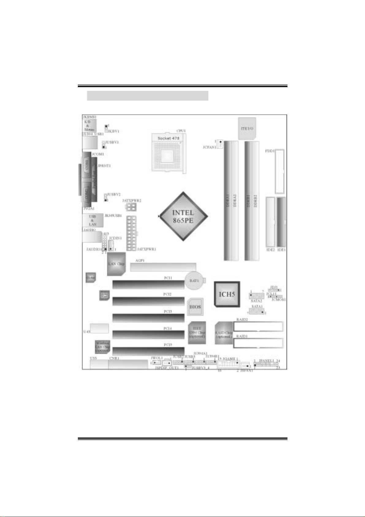
1.3 LAYOUT OF P4TSE (VERSION 1.0)
Note: ● represents the 1st pin.
6
PP44TTSSEE
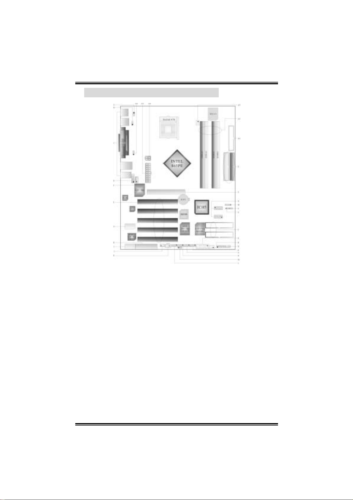
1.4 COMPONENTS OF P4TSE (VERSION 1.0)
JKBV1: Power Sourc e Selection for
A.
Keyboard/ Mouse
JU SBV1: Power Source Selection f or
B.
USB
Back Panel Connec t ors
C.
JAU DIO1: Front Audio Header
D.
PCI 1-5: Peripheral C om ponent
E.
Int erc onnect Slots
JCDIN1: CD-ROM Audio- In Header
F
U43: Wireless Audio Connector
G.
CN R1 : Co mmun i cation Ne twor k
H.
Riser Slot
U33: Wireless LAN Connector
I.
JW OL1: W ak e On LAN Header
J.
JSPD IF_OU T1: Digit al Audio
K.
Connector
JUSB2: Front USB Header
L.
JU SBV3_4: Power Source Selection
M.
for U SB
JUSB3: Front USB Header
N.
J1394A1: Front 1394 Header
O.
(optional)
J1394B1: Front 1394 Header
P.
(optional)
JPANEL1: Front Panel Connect or
Q.
JSFA N1: S ystem Fan Header
R.
JGAME1: Gam e Port H eader
S.
RAID1-2 : Raid Connectors
T.
JC L1: Case Open C onnector
U.
JCM O S 1 : Cl e a r CMOS Ju mp e r
V.
JDJ1: Audio D J Connector
W.
SATA1-2: Serial ATA C onnectors
X.
AGP1: Accelerated Graphic Port Slot
Y.
ID E1-2: Hard Dis k Connectors
Z.
FDD1: Floppy D isk Connect or
A1.
DD RA 1 - 2 /DDRB1 - 2: DDR DIMM
A2.
Modules
JCFAN 1: C PU Fan Connect or
A3.
JATXPWR2: ATX Power Connec t or
A4.
JATXPWR1: ATX Power Connec t or
A5.
JU SBV2: Power Source Selection for
A6.
USB
7
PP44TTSSEE
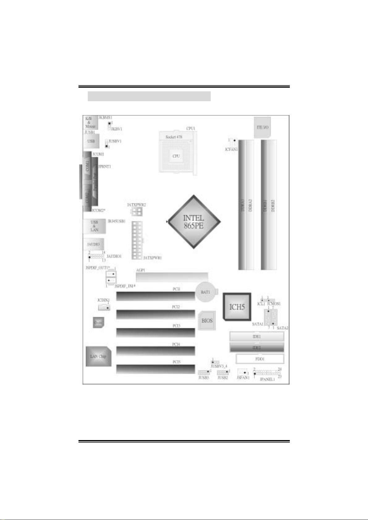
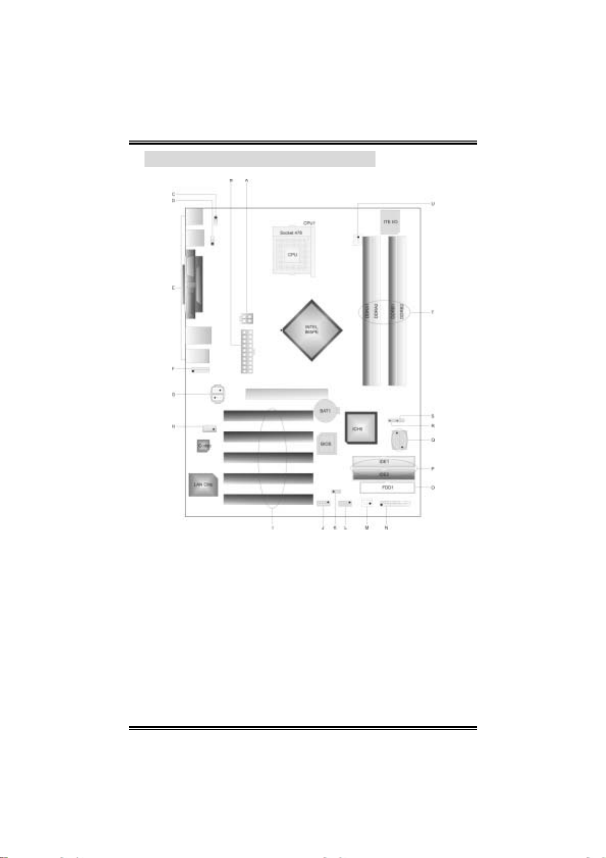
1.5 LAYOUT OF P4TSE (VERSION 7.X)
Note: “●” represents the 1st pin, and “*” r eprese nt s f or optional.
8
PP44TTSSEE
1.6 COMPONENTS OF P4TSE (VERSION 7.X)
JATXPWR2: ATX Power Connec t or
A.
JATXPWR1: ATX Power Connec t or
B.
JKB_USBV1: Pow er Sou r ce
C.
Selection f or Keyboard/ mouse
and U SB
JU SBV2: Power Source Selection f or
D.
USB
Back Panel Connec t ors
E.
JAU DIO1: Audio H eader
F
JSPD IF_OU T1/ IN 1: Digital Audio
G.
Connec t or (optional)
JCDIN1: CD-ROM Audio- In Header
H.
PCI 1-5: Peripheral C om ponent
I.
Int erc onnect Slots
JUSB3: Front USB Header
J.
JU SBV3_4: Power Source Selection
K.
for U SB
JUSB2: Front USB Header
L.
JSFA N1: S ystem Fan Header
M.
JPANEL1: Front Panel Connect or
N.
FDD1: Floppy D isk Connect or
O.
ID E1-2: Hard Dis k Connectors
P.
SATA1-2: Serial ATA C onnectors
Q.
JC L1: Case Open C onnector
R.
JCM O S 1 : Cl e a r CMOS Ju mp e r
S.
DD RA 1 - 2 /DDRB1 - 2: DDR DIMM
T.
Modules
JCFAN 1: C PU Fan Connect or
U.
9
PP44TTSSEE
CHAPTER 2: HARDWARE INSTALLATION
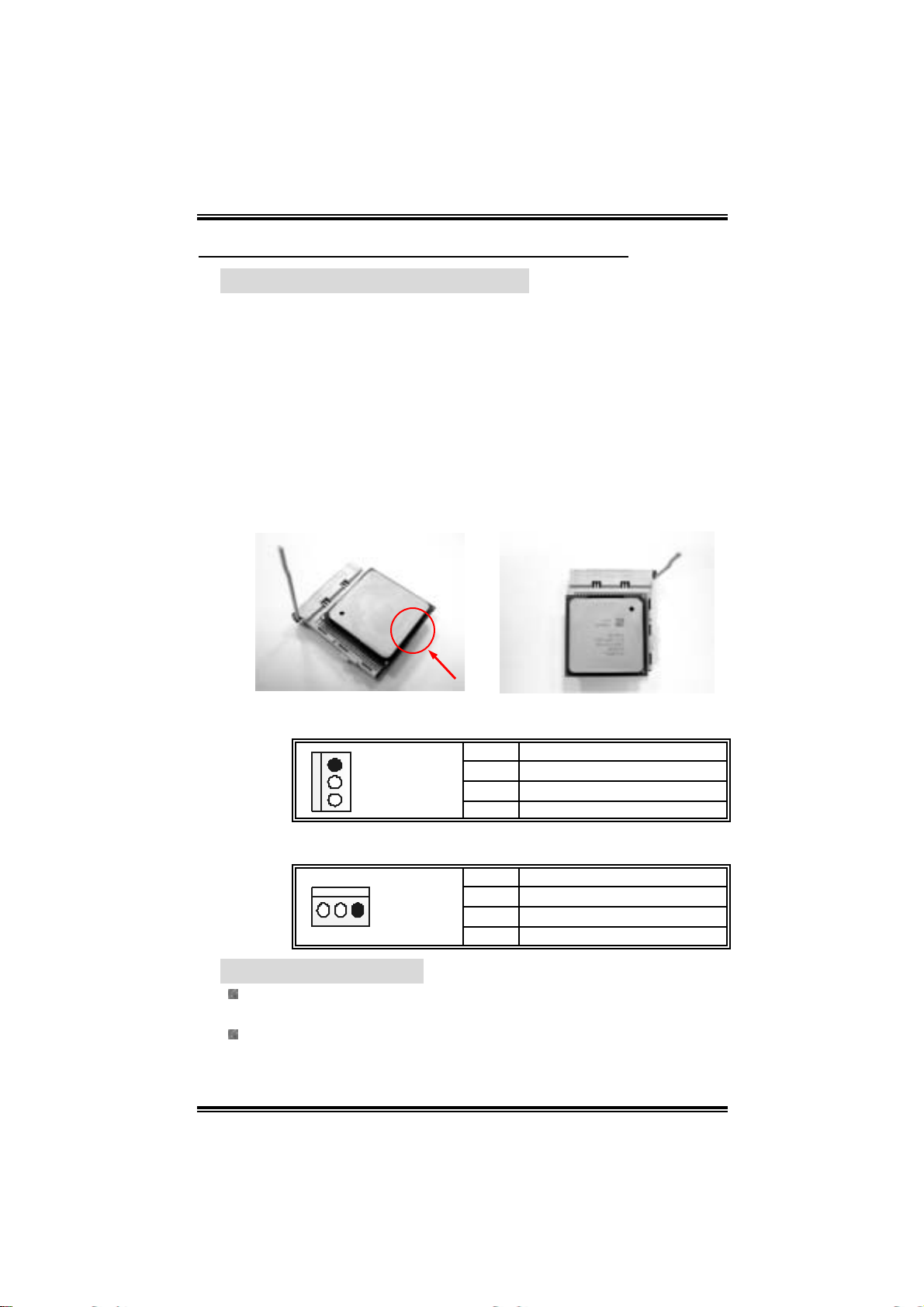
2.1 CENTRAL PROCESSIN UNIT (CPU)
Step 1: Pull the lever sideways away from the socket and then raise
the lever up to a 90-degree angle.
Step 2: Look for the white dot/cut edge. The white dot/cut edge should
point wa rds th e lever pi vot. The CPU will fit onl y in the corre c t
orientation.
Step 3: Hold the CPU down fi rmly, and then cl ose the lever to com plete
the i nstal la ti on.
Step 4: Put the CPU F an on t he CP U and buckl e it . Co nn ec t the CP U
FAN power cable to the JCFAN1. This completes the
installation.
CPU FAN He ader: JC FAN1
1
JCFAN1
Pin Assignment
1 Ground
2 +12V
3 FAN RPM rat e sense
System Fan Header: JSFAN1
Pin Assignment
1 Ground
1
JSFAN1
2 +12V
3 FAN RPM rat e sense
2.2 MEMORY MODULES
Supp orts up to fo r DDR DI MMs (2 DIMMs per cha nnel ),
single-sided and/or double-sided.
For dual channel operation, DIMMs must be populated in identical
pairs. This has to be the combin ation of DDRA1+ DDRB1 (blue
DIMMs) o r DDRA2+DDRB2 (whit e DIMMs).
10
PP44TTSSEE
Dual Channel Guidelines
¾ Matched DIMM configuration in each channel:
- Sam e Dens ity (128 MB, 25 6M B, 512 MB , or 1GB… etc .)
- Sam e DR AM tec hnology ( 128M bit, 256M bit, or 512M
bit)
- Same ERAM bus width (x8 or x16)
- Both either single-sided or dual-sided.
¾ Matc hed in bot h Chan ne l A a nd B me mor y s lots.
- Populate symmet rical memory sl ots.
¾ Optimal platform pe rf ormance wit h dual c ha nnel, DDR400 ,
matched DIMMs:
- Full y loaded configurations can be singl e or
double-sided DIMMS.
- Lightly l oad ed con fi gur a t ions need to be doub le-sid ed
DIMMS.
¾ W hen not usin g DDR400, best performance obtained wit:
- Sy m metrical D IMM population and m atched
double-sided DIMM s
- Lightly loaded configuration.
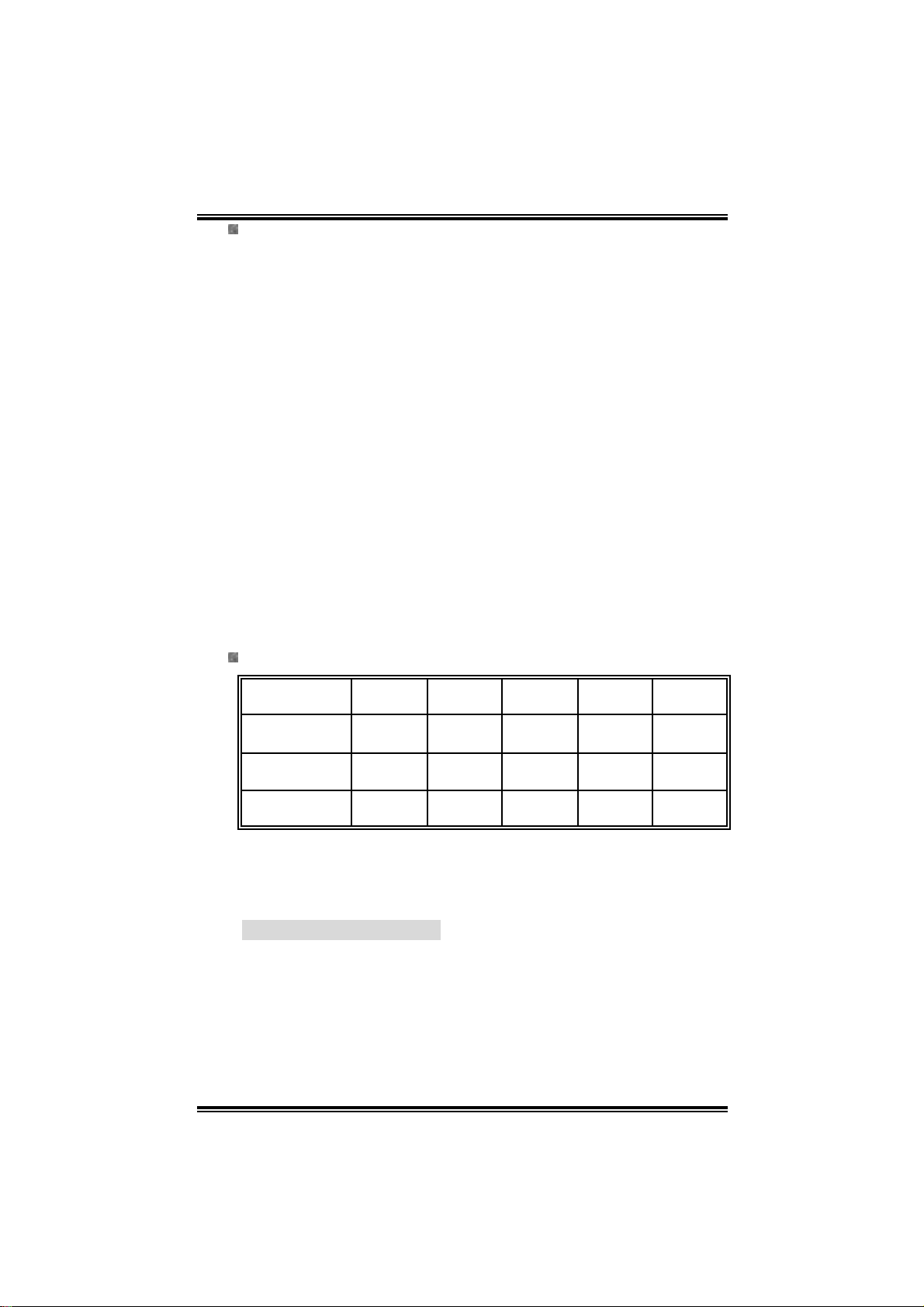
Dual Channe l Configuration Table
D IMM Slot
Li ghtly Loaded
Config.
Li ghtly Loaded
Config.
Fully Loaded
Config.
DDRA 1 DDRA 2 DDRB 1 DDRB 2
128MB ~
1GB
128MB ~
128MB ~
1GB
128MB ~
1GB
1GB
128MB ~
1GB
128MB ~
128MB ~
1GB
256MB ~
1GB
128MB ~
1GB
System
Density
2GB
256MB ~
2GB
256MB ~
2GB
* DRAM Access Tim e: 2.5V unbuffered/ no regi stered (wi thout ECC)
DDR SDRAM PC21 00/2700/32 00 ty pe req uired.
* DRAM type: 128MB/256MB/512MB/1GB DIMM M odule (184 pin).
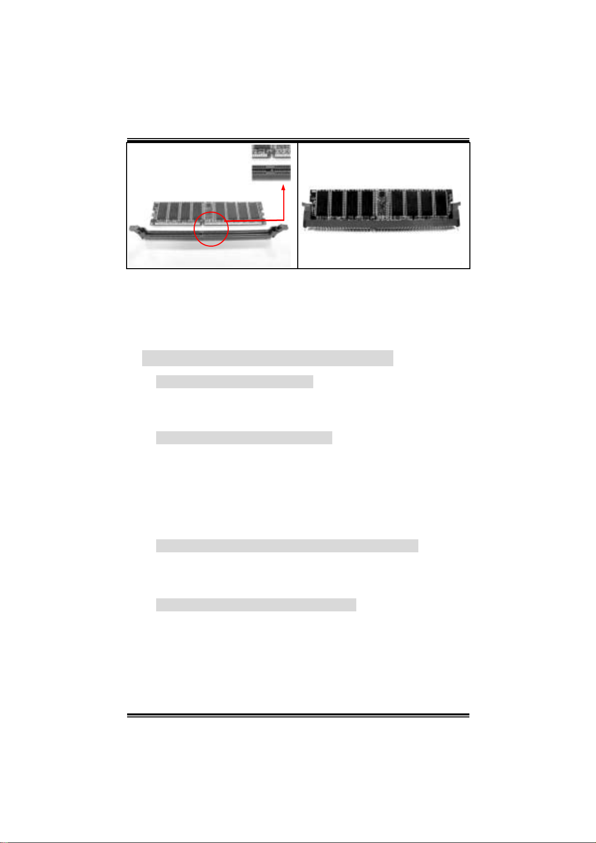
DDR Modu le ins tallation
1. Unlock a DIMM slot by pressing the retaining clips outward. Align a
DIM on the slot such that the notch on the DIMM matches the
break on the Slot.
2. Insert the DIMM vertically and firmly into the slot until the retaining
chip snap back in place and the DIM M is properly seated.
11
PP44TTSSEE
Note:
" DDR DIMM" ----Note! : To assure t he system safety , if you need to
ch ange DDR modules, fi rstly, please unpl ug the 20-pin po wer cable
with the power connector, then you can change the m odules.
Afterwards, plug the cable wi th the power connector, and finally you
can boot up the system.
2.3 JUMPERS, HEADERS, CONNECTOR S, & SLOTS
Floppy Disk Connector: FDD1
The motherboard provi des a standard floppy disk connector that
s uppor t s 360K , 720 K, 1.2 M, 1.44 M and 2. 8 8 M f lo ppy d is k types. Th is
connector supports the provided floppy drive ribbon cables.
Hard Disk Connectors: IDE1/ IDE2
The motherboard has a 32-bit Enhanced PCI IDE Controller that
provides PIO Mode 0~5, Bus Master, and Ul tra DMA 33/ 66/ 100
functio nalit y. It ha s two HDD c onne c to rs IDE1 (primary) an d IDE2
(secondary).
The IDE connectors can connect a master and a slave drive, so you
can connect up to four hard disk drives. The first hard drive should
al ways be con nected to IDE1.
Peripheral Component Interconnect Slots: PCI 1-5
This motherboard is equipped wi th 5 standard PCI sl ots. PCI stands for
Peripheral Component Interconnect, and it i s a bus standard for
expansi on cards. T his PCI slot is designated as 32 bits.
Accelerated G raphics Port Slot: A GP1
You r mon itor will atta c h dire c tly to that vide o card. Thi s motherbo ard
supports video cards for PCI slots, but it is also equipped with an
Accelerated Graphics Port (AGP). An AGP card will take advantage of
AGP technology for improved video efficiency and performance,
especially with 3D graphics.
12
PP44TTSSEE
Commun icati on Netw ork R iser Slot: CNR1
( Ver s ion 1.0 on ly, and none for Version 7.x)
The CNR specification is an open In du stry Standard Archi tec ture, an d it
defi nes a hardware scalable riser card i nterface, which supports
modem onl y.
Serial ATA Connector: JSATA1/ JSATA2
The motherboard has a PCI to SATA Controller with 2 channels SATA
interface, i t satisfies the SATA 1.0 spec and with transfer rate of
1.5Gb/s.
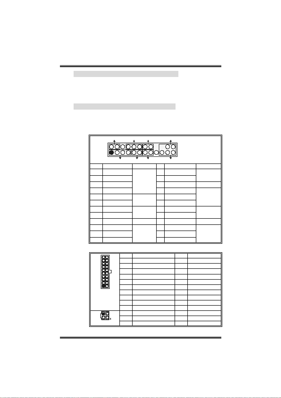
F r ont Pa n el Conn ector: JPA N EL1
PWR_LED
SLP
224
123
IRON/OFF
SPK
HLED
RST
IR
JPANEL1
Pin Assignment Function Pin Assignment Function
1 +5V 2 Sleep control
3 N/A 4 Ground
5 N/A 6 N/A N/A
7 Speaker
9 HDD LED (+) 10 Power LED (+)
11 HEE LED (-)
13 Ground 14 Power button
15 Reset control
Speaker
Connector
Hard driv e
LED
Reset
button
8 Power LED (+)
12 Power LED (-)
16 Ground
17 N/A 18 Key
19 N/A 20 Key
21 +5V 22 Ground
23 IRTX
IrDA
Connector
24 IRRX
Pow er Conn ector s: JATX PWR1/PAT X PWR2
1
123
20
Pin Assignment Pin Assignment
1 +3.3V 11 +3.3V
2 +3.3V 12 -12V
3 Ground 13 Ground
4 +5V 14 PS_ON
5 Ground 15 Ground
6 +5V 16 Ground
11
7 Ground 17 Ground
8 PW_OK 18 -5V
9 Standby Voltage +5V 19 +5V
10 +12V 20 +5V
Pin Assignment Pin Assignment
1 +12V 3 Ground
2 +12v 4 Ground
10
JATXPWR1
JATXPWR2
Sleep butt on
Power LED
Power-on
button
IrDA
Connector
13
PP44TTSSEE
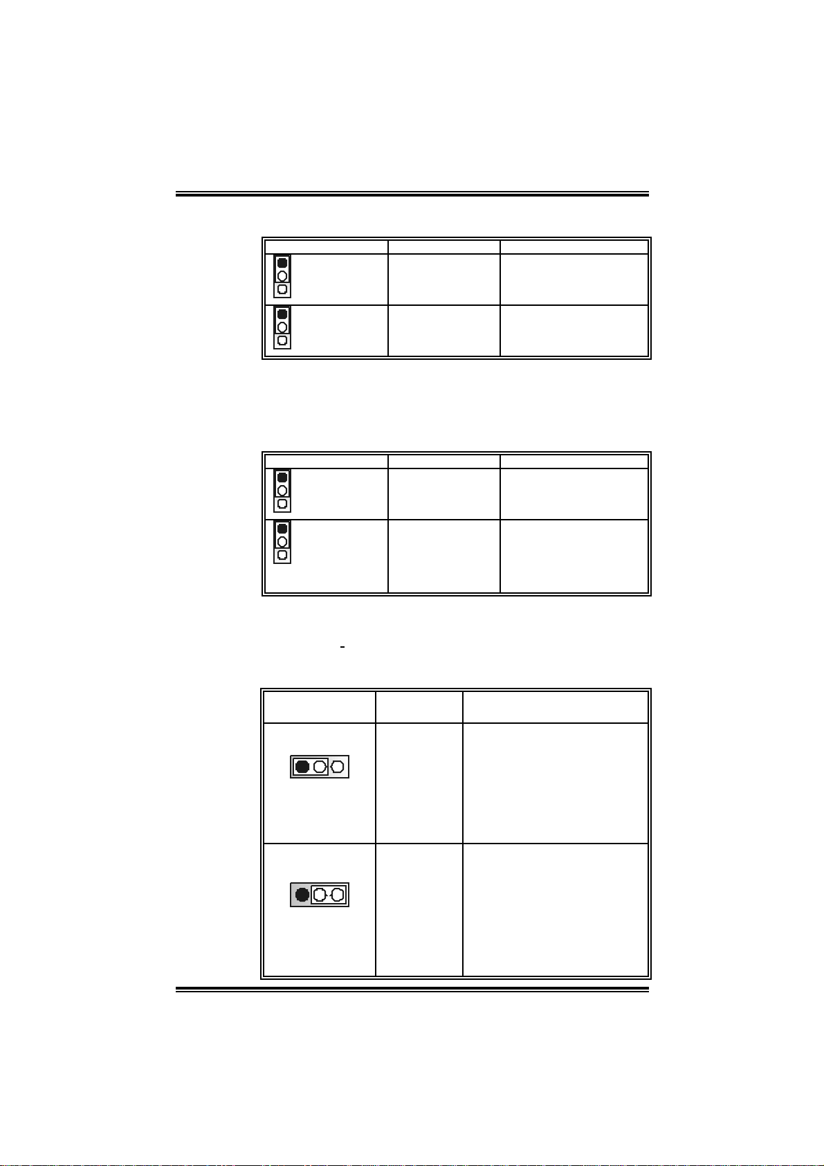
Power Sourc e Se lect io n for Keyboard / M ou s e: JKBV1
(For version 1.0 only)
JKBV1 Assignment Description
1
3
Pin 1-2 close
1
3
Pin 2-3 close
+5V
+5V Standby
Voltage
+5V for PS /2 keyboard
and PS/2 mouse.
PS/2 k eyboard and PS/ 2
mous e are powered with
+5V st andby voltage.
Note:
In order to support this function “Power-on s ystem via keyboard and
mous e”, “JKBV1” jumper c ap should be plac ed on Pin 2-3.
Power Sourc e Se lect io n for Keyboard / M ou s e: JKB_U S BV 1
(For version 7.x only)
JKBV1 Assignment Description
1
3
Pin 1-2 close
1
3
Pin 2-3 close
+5V
+5V Standby
Voltage
+5V for PS /2 keyboard/
mous e and USB at the
JUSB1 connector port.
PS/2 k eyboard / m ouse
and USB at t he JUSB1 at
the JUSB1 connector port
are powered wit h +5V
standb y voltage.
Note:
In order to support this function “Power-on s ystem via keyboard and
mous e”, “JKB
USBV1” jumper c ap should be plac ed on Pin 2-3.
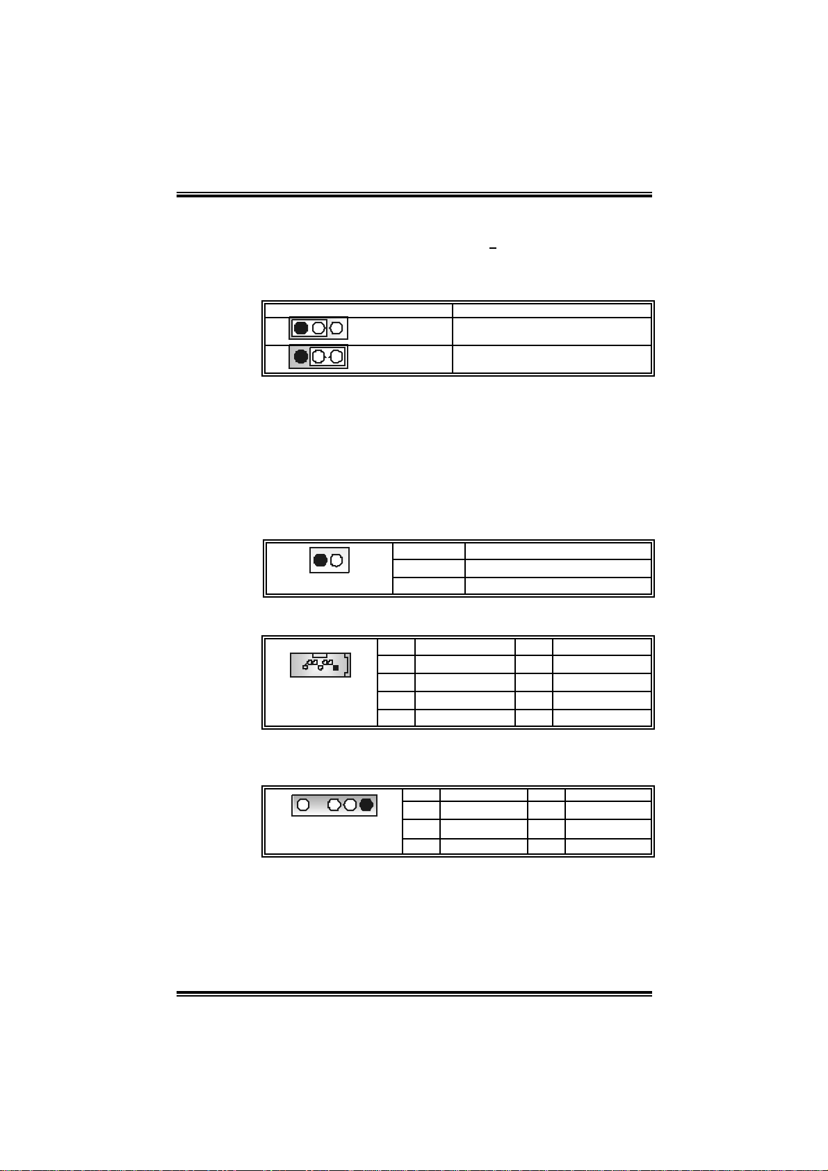
Power Source Select ion for USB: JUSBV1/JUSBV2/JUSBV3_4
(JUSB VI for ve rsion 1.0 only)
JUSBV1/USBV2/
JUSBV3_4
1 3
Pin 1-2 close
1 3
Pin 2-3 close
Assignment Description
JUSBV1: +5V for USB at the
JUSB1 connector port.
JUSBV2: +5V for USB at the
+5V
JRJ45USB1 connector
port.
JUSBV3_4: +5V for USB at the
JU SB 2/3 c onnector
ports.
JU SBV1: JUSB1 port powered
with standby v oltage of
5V
+5V st andby
Voltage
JU SBV2: JRJ45USB1 port
powered wit h standby
volt age of 5V
JU SBV3_4: JUSB2/3 ports
powered wit h standby
volt age of 5V
14
PP44TTSSEE
Note:
In order to support this function “Power-o system via USB
device,” “JUSBV1/JUSBV2/JUSBV3_4” jumper cap should be
plac ed on Pin 2-3 individually.
Clos e CMOS Jumper: JCMOS1
JCMOS1 Assignment
1 3
1 3
Pin 1-2 close
Pin 2-3 close
Norm al O\operation (Def ault ).
Clear CMOS data.
※ Clear CMOS Procedures:
1. Remove AC power line.
2. Set the jumper to “Pin 2-3 cl ose”.
3. Wait for fi ve seconds.
4. Set the jumper to “Pin 1-2 cl ose”.
5. Power on the AC.
6. Reset your desi red password or clear the CMOS data.
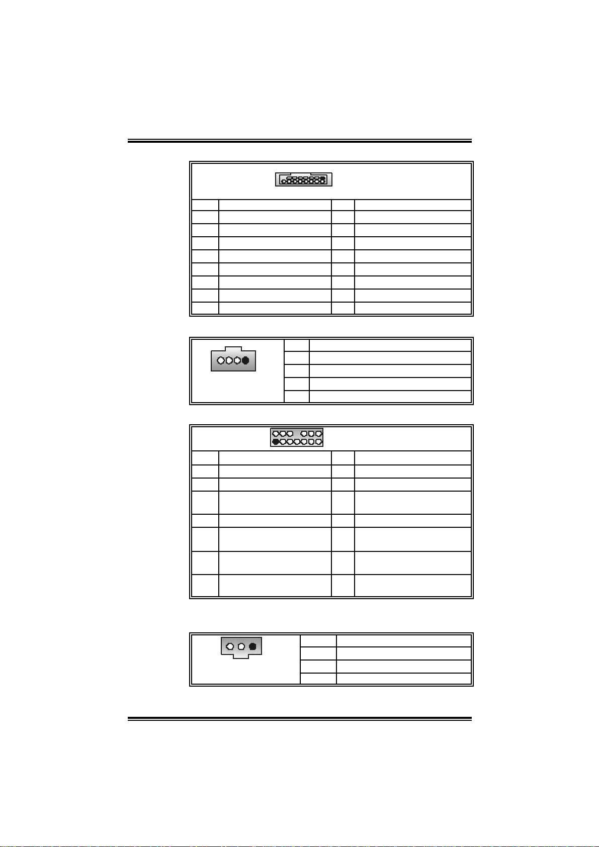
Case Op en Connector: JCL1
12
JCL1
Pin Assignment
1 Cas e open signal
2 Ground
Se rial ATA co nnector JSATA1/JS ATA2
Pin Assignment
1 Ground 2 TX+
1234567
JSATA1/JSA TA2
3 TX- 4 Ground
5 RX- 6 RX+
7 Ground
AUDIO DJ Conn ector: JD J1
(For version 1.0 only)
Pin Assignment Pin Assignment
1 SMBDATA 2 SMBCLK
15
JDJ1
3 INT_B 4 Key
5 AXT_PWROK
Pin
Assignment
15
PP44TTSSEE
Game He ader: JGAME1 (For version 1.0 only)
15
Pin Assignment Pin Assignment
1 +5V 2 +5V
3 Joy stick B butt on 1 4 Joy stick A button 1
5 Joy stick B coordinat e X 6 Joystick A c oordinate X
7 MIDI output 8 Ground
9 Joy stick B coordinat e Y 10 Ground
11 J oy stick B button 2 12 J oy stick A coordinate Y
13 MID input 14 J oy stick A button 2
15 N/A 16 +5V
1
216
JGAME1
CD- ROM A udio- in H e ader: J CDI N 1
JCDIN1
Pin
1
1 Lef t channel input
2 Ground
3 Ground
4 Right channel input
Assignment
Front Panel Audio Header: JAUDIO1
2
1
Pin Assignment Pin Assignment
1 Mic in/center 2 Ground
3 Mic power/Bass 4 Audio power
Right line out/ Speaker
5
out R ight
7 Reserved 8 Key
Lef t line out/Speaker out
9
Lef t
Right line in/R ear
11
speaker Right
Lef t line in/R ear speak er
13
Lef t
14
13
JAUDIO1
Right line out/ Speaker out
6
Right
Lef t line out/Speaker out
10
Lef t
Right line in/R ear speaker
12
Right
Lef t line in/R ear speak er
14
Lef t
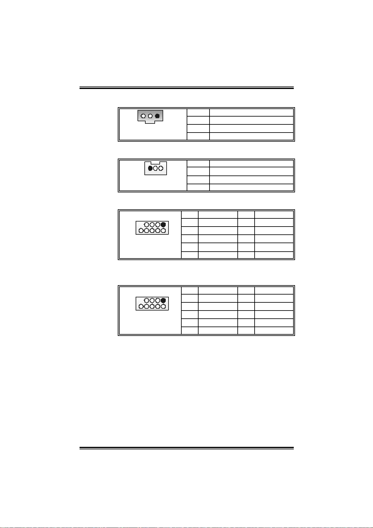
Digita l Aud io Connector: JSPDIF _OUT 1
(Optional for Version 7.x)
1
JSPDIF_OUT1
Pin
1 +5V
2 SPDIF_OUT
3 Ground
16
Assignment
PP44TTSSEE
Dig i ta l Audio C on n ec tor: JS PD I F _I N 1
(Opti onal fo r Version 7.x,and none fo r ve rsion 1 .0)
JSPDIF_IN1
1
Pin
1 +5V
2 SPDIF_IN
3 Ground
Assignment
Wake on LAN Header: JWO L1 (For ver s ion 1.0 only)
1
JWOL1
Pin
1 +5V_SB
2 Ground
3 Wake-up
Assignment
Front USB Heade r: JUSB2/3
9
10
JUSB2/3
Pin
Assignment
1 +5V (fused) 2 +5V (fused)
1
3 USB- 4 USB-
2
5 USB+ 6 USB+
7 Ground 8 Ground
9 Key 10 NC
Pin
Assignment
F r ont 13 94 He ader: J1 39 4A 1/J139 4B1
(Opti onal fo r Version 1.0 only, and none for Ve rsi on 7 .x)
9
10
J1394A1/J1394B1
1
2
Pin
Assignment
1 A+ 2 A3 Ground 4 Ground
5 B+ 6 B7 +12v 8 +12V
9 Key 10 Ground
Pin
Assignment
17
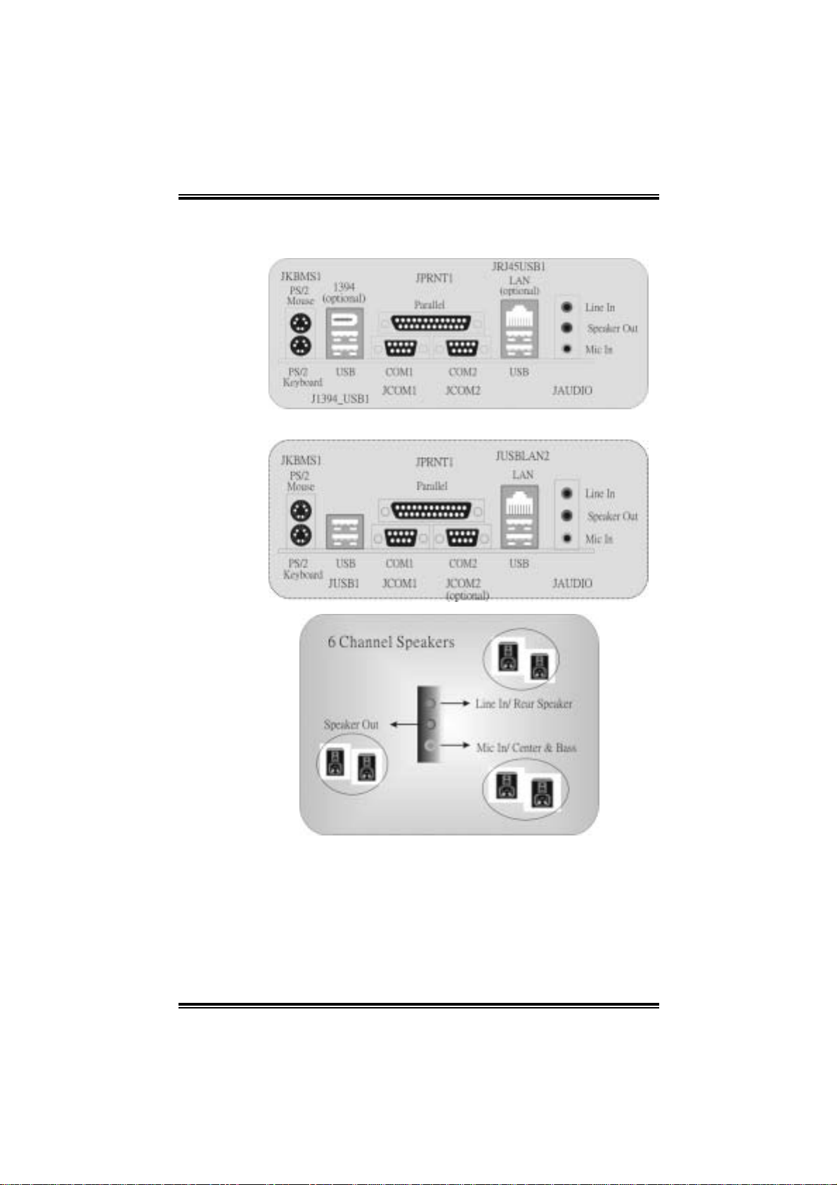
Bac k Panel Connectors
V ersi on 1.0
V ersi on 7.x
PP44TTSSEE
18
 Loading...