


CD 7

ALPHA 7/8/9 CD SERVICE MANUALALPHA 7/8/9 CD SERVICE MANUAL
Arcam Alpha 7/8/9 CD Service Manual
Issue 1 Serial No. 0001 - (Paul Newton July 96)
Circuit Description
The following notes describe the operation of the
Alpha 7/8/9 CD players. They include the circuitry on
the main, DAC and display PCBs but not that on the
servo PCB attached to the mechanism.
Power Supplies
The mains input is fitted with inductors L2,3,6,7 to
filter electromagnetic interference coming out of the
player.
Mains transformer T201 has three secondary
windings supplying two separate power supplies and
an AC supply for the display filament:
Analogue Supply
Bridge rectifier D4,5,6,7 and reservoir capacitors
C209-C212 produce unregulated split rails of about
+/-22V.
Z204 and Z205 provide regulated outputs of +18V
and -18V respectively that power the opamps in the
audio output stage.
Since there is no power switch on this secondary, the
analogue supplies are always connected.
Digital Supply
Switch SW201-A disconnects the digital secondary
winding when the 'Power' switch is out.
An unregulated supply of about 11V is produced by
the bridge rectifier D8,9,10,11 and reservoir
capacitor C36.
This is then regulated to provide three +5 volt
supplies (Z208 general logic supply, Z207 DAC
supply, Z203 system clock generator supply) and a
+7.3v supply for themechanism and motor drive
circuits(Z206).
A -30v supply is formed by Z209 and associated
components to power the display grid.
Muting
When the unit is turned off SW201-A discharges
capacitor C29 quickly. This along with the AMUTE
signal from the microprocessor, controls the output
mute transistors Q1,101 via level shifter Q3.
Clock Generator
The system clock is generated by a discrete oscillator
based around Q2 and 16.9344MHz oscillator X1. The
output of Q2 is amplified and buffered by inverters
Z202-E & D and sent to the clock input of the DAC
Z201.
DAC & Audio Outputs (Alpha 7 only)
The DAC is a Delta-Sigma design from Burr Brown,
the PCM1710U.
The serial digital data from the decoder Z206 is input
to pins 1 to 3. The system clock is input to pin 5.
The DAC is powered entirely from one 5V supply,
although it is split and decoupled between the
analogue and digital sections of the device.
The analogue outputs from each channel are
processed identically.Three poles of filtering are
provided by the active filter based around Z1-A. Z1-B
buffers the audio output and sets the output level.
Muting is provided by turning on Q1 and Q101.
DAC & Audio Outputs (Alpha 8 only)
This is a similar circuit as the one used on the Arcam
Alpha 6 DAC PCB but designed for Sony format
input data and a better digital filter, the SM5843AP1,
Z14.The digital filter is used with a SM5864AP 20-bit
DAC chip, Z12, (described here as a PWM noise
shaper to avoid confusion with the 1-bit DAC Latch
which follows it). The output from this is re-latched by
Z7, Z8.
Digital FilterA PIC micro on the mother board
controls the filter with the signals RB0 to RB7. The
SM5843 filter has internal pull-up resistors on its
inputs resulting in RB4 & RB5 being logic 1.
The SM5843APT requires several control lines from
the PIC...
RB7 FSEL2, Selects sampling rate for de-emphasis.
Static low for 44.1K.
RB6 FSEL1, Selects sampling rate for de-emphasis.
Static low for 44.1K.
RB5 IW2N, Selects input word length. Static high for
16 bits.
RB4 MDT, Serial data input for volume control. Burst
at switch-on for setting to full.
RB3 RSTN, Reset line. Short pulse low at switch on,
then static high.
RB2 MLEN, Serial data latch input for volume
control.
RB1 MCK, Serial clock input for volume control.
RB0 Not connected.
No Dither On Silence
The digital filter adds ‘dither’ to the output signal.
This improves the low-level performance of the DAC.
The PWM filter normally mutes when it detects
digital silence to prevent any unwanted noise and
idle-tones on the audio outputs when no music is
playing. A slight click is audible when this happens.
Unfortunately, the added dither prevents this mute
from operating because it holds it open. Q11 detects
digital silence on the data input to the filter. When
silence is detected, the dither function is switched off
ALPHA 7/8/9 CD SERVICE MANUALALPHA 7/8/9 CD SERVICE MANUAL
16.9344MHz Low-Jitter
System Clock, X1, Q5 & Z13
SM5843AP1
Digital Filter,
Z14
74HC74
Latches,
Z7 & Z8
SM5864 PWM
Noise Shaper, Z12
Analogue Filter,
Z1, Z2, Z3, Z4
Sony Format Digital
Audio
Control from PIC micro
(Z211) on main pcb
Audio out
Clock
Block Diagram of Alpha 8 DAC PCB
allowing the PWM filter’s mute to operate as normal.
Mute Relay
The mute relay is controlled from the PIC micro via
RA0 after switch-on. In Standby mode, XRST is low
which interrupts the relay via Q9. RA0 is low when
the CD player comes out of standby mode and goes
high after a short settling delay.
The power rail, RLYPWR, is un-regulated and has a
small reservoir capacitor (on the mother board) so
that the relay is released very soon after the mains is
disconnected from the CD player before the other
power supply rails collapse.
PWM noise shaper
To reduce EMC, the clock signal going into this chip,
Z12, is very weak on the XTI pin (23) pin, taken
directly off Q5. This is amplified so that there should
be a larger signal on the CKO pin (26).
The PWM output on pins 11, 13, 16 and 18 can be
resolved into an audio waveform on a scope simply
by measuring them through a 100K resistor. The
same is true for the PWM signals through the latch
and the level shifter.
Latch
The PWM data from Z12 is re-latched using 74HC74
latches, Z7 and Z8.The power supply for these chips
is the DAC voltage reference and the output drives
the analogue filter stage directly. The latches reduce
any edge-timing jitter induced on the PWM signal
coming from Z12.
Analogue filter
The first half of the analogue filter, Z3 and Z4 is
balanced. The signal through one side of the op-amp,
pin 1, should be phase inverted with respect to the
other, pin 7. These signals should be viewed on a
scope through a 100K resistor since there may still
be quite a lot of RF noise on the signal.
Z1 and Z2 filter the audio signal further and also
convert the balanced signal into a single ended
signal. Z18 acts as a DC servo to reduce the output
offset voltage. This has a very large time constant so
an offset as high as 50mV is possible when the unit
is first plugged in. This reduces to less than 3mV
after 10 minutes and stays low if the unit is switched
off and on with the Standby button.
ALPHA 7/8/9 CD SERVICE MANUALALPHA 7/8/9 CD SERVICE MANUAL
Test Points Marked on Circuit Diagram Only
Test Points Measurement Information
17MHz
Clock Output to mother board. 16.9344MHz +/- 40ppm, 4V to 5V peak to peak square wave.
AGND
Analogue ground point.
AMUTE
Digital audio mute input on SK203. 0V=off, 5V=Mute.
CK
Serial Data clock input on SK203. Sony format.
DA
Serial Data data input on SK203. Sony format.
CLKSYNC
Crystal clock override. A 16.9344MHz HCMOS clock can be injected from an external source.
DEEM
De-emphasis select input on SK203. 0V=off, 5V=On.
DGND
Digital ground point.
LOUT
Left channel audio output at SK1. Measure d.c. offset at switch-on and after 1 minute, see specifications.
LR
Serial Data LR input on SK203. Sony format.
MUTERLY
Mute Relay Voltage. Equal to RLYPWR voltage when output is muted and 0V d.c. +0.5V,-0.0V when
output is un-muted.
N15
Regulated analogue supply. -15V d.c. +/- 0.6V.
N18V
-18.45V d.c. +/- 0.5V supply input on SK204 for analogue.
P5V(0)
+5V d.c. +/- 0.3V digital filter supply input on SK204.
P5V(1)
+5V d.c. +/- 0.3V PWM noise shaper supply input on SK204.
P5VCLK
Regulated clock supply. +5V d.c. +/- 0.3V.
P15
Regulated analogue supply. +15V d.c. +/- 0.6V.
P18V(0)
+18.45V d.c. +/- 0.5V supply input on SK204 for analogue.
P18V(1)
+18.45V d.c. +/- 0.5V supply input on SK204 for clock and latch.
PWRGND
Power ground point. Used by mute relay only.
RA0
Mute relay control from PIC micro on SK203.
RB0-RB7
Control lines from PIC micro on SK203.
REFL
DAC reference voltage, left channel. +5V +/- 0.3V.
REFR
DAC reference voltage, right channel.
RLYPWR
+12V d.c. +/- 1V supply input for mute relay on SK204.
ROUT
Right channel audio output at SK1. Measure d.c. offset at switch-on and after 1 minute, see
specifications.
SRVL
Left d.c. servo voltage. -10 to +10V d.c.
SRVR
Right d.c. servo voltage.
SYSCLK
Clock used by latches. 4V to 5V peak to peak square wave at 16.9344MHz.

ALPHA 7/8/9 CD SERVICE MANUALALPHA 7/8/9 CD SERVICE MANUAL
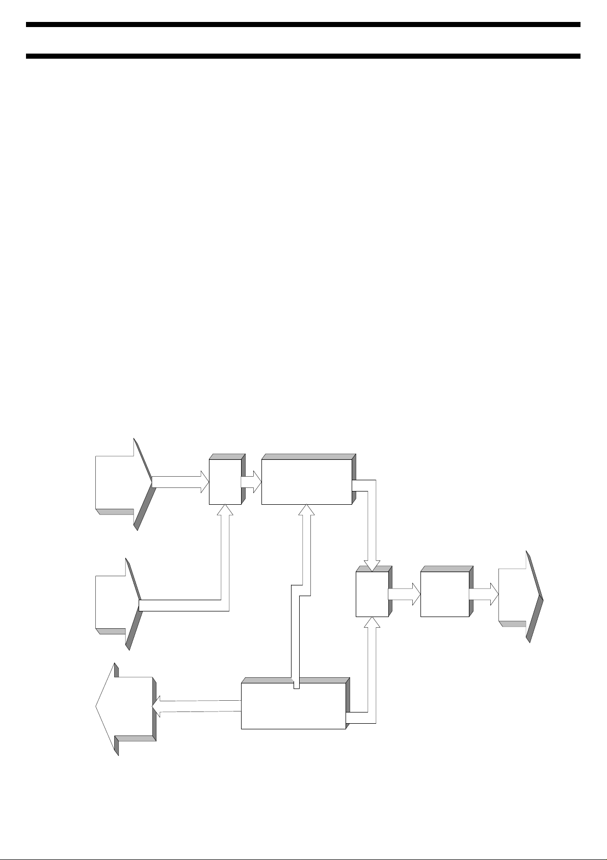
Disc Transport Module
The CDM 14 module comprises the disc loading
mechanism, laser assembly, RF amplifier and
analogue signal processing. All the servo control and
motor drive circuits are also included.
Digital Signal Processor
Mute, attenuation and de-emphasis functions are
controlled via a three-wire serial bus from the system
controller (Z212) to pins 26, 27 & 28 of the DAC
(Z201).
Digital audio is input to the DAC on pins 1, 2& 3 in
standard Sony format i.e. Word Clock, Data and Bit
Clock.
A digital output complying to the SPDIF standard is
generated by the decoder on the mechanisim
assembly. This is passed through an isolating
transformer, T202, to the digital output socket SK5.
System Controller
The CXP826P16Q system controller (Z212) is a
combined CD player controller, keyboard scanner,
remote control decoder and fluorescent display
driver. It's clock is generated by 4.00MHz resonator
X201.
The controller detects the position of the disc drawer
from the status of two microswitches, INSW &
OUTSW, on socket SK205. The drawer motor is
controlled via motor driver Z210
The keyboard scanning works by connecting the keys
to a resistor ladder on an ADC (analogue to digital
convertor) input to the microcontroller. Pressing a
key presents a unique voltage to this input.
The signal from the remote control receiver is input
to RMIN (pin 2) after first passing through the PIC
microcontroller, Z211, on the small remote receiver
pcb. This PIC ic converts the RC-5 format codes
from the remote control handsets to NEC data,
suitable for the Sony chipset. It also controls
theconfiguration of the digital filter/DAC on the Alpha
8 and 9 DAC boards the The remote control data
contains a ‘customer code’ that identifies it as an
Arcam product.The microcontroller is confiqured to
accept this code by means of the diode network
D291 to D297.
Disassembly For Servicing
To remove the boards within the CD players follow
the instructions below.
1. Remove the top cover.
2. Press load to eject the CD tray.
3. Unplug the unit from the mains.
4. Push the tray front upwards to remove it
from the tray. Push the tray in manually.
5. Remove the 4 screws holding the front panel
to the chassis and release the locating tabs.
6. Unplug the flexfoil from the display board
where it enters the main pcb.
7. Remove the 2 screws holding the remote
receiver pcb in place.
8. The front panel can now be pulled off the
unit.
9. To remove the display pcb remove the 6
screws holding the board in place.
To remove the main pcb first remove the DAC board
if it is an Alpha 8 or 9 CD player.
1. Remove the 3 screws holding the audio
output sockets to the rear panel and 2
screws holding the aluminium extrusion in
place.
2. Squeeze the tops of the 2 pcb pillars and lift
the board up slightly to clear them .
3. Remove the 2 flexfoils from the DAC board.
The DAC board, still attached to the extrusion, can
now be removed from the unit.
To remove the main pcb remove the 8 pcb securing
screws and the screw holding the digital ouput socket
to the chassis. (On Alpha 7 CDs also remove the 3
screws securing the audio ouput sockets in place).
Release the cables which connect the mechanism to
the main board.
The main pcb can now be slid out of the case.
ALPHA 7/8/9 CD SERVICE MANUALALPHA 7/8/9 CD SERVICE MANUAL
Alpha 7/8/9 Main PCB Parts List
Ref. No. Description Part No.
C2 PPRO 680P 63V 5% RA 2D168
C3 PPRO 680P 63V 5% RA 2D168
C4 ELST NON POLAR 10UF 35V 2U610
C5 PPRO 100P 63V 5% RA 2D110N
C6 PPRO 680P 63V 5% RA 2D168
C7 PPRO 680P 63V 5% RA 2D168
C10 CERD 1N0 63V 2A210
C11 CERD 10N 100V 20% 2A310
C12 CERD 10N 100V 20% 2A310
C13 CERD 33P 63V 2A033
C14 CERD 33P 63V 2A033
C15 CERD 100P 63V 2A110
C16 CERD 100P 63V 2A110
C17 CERD 10N 100V 20% 2A310
C18 CERD 10N 100V 20% 2A310
C19 CERD 10N 100V 20% 2A310
C20 PPRO 680P 63V 5% RA 2D168
C21 ELST NON POLAR 10UF 35V 2U610
C22 ELST 100U 25V 2N710
C23 ELST 100U 25V 2N710
C24 ELST 100U 25V 2N710
C25 ELST 22U 20V OSCON 2P622
C26 ELST 100U 25V 2N710
C27 ELST 10U 50V 2N610
C28 CERD 470P 63V 2A147
C29 ELST 100U 25V 2N710
C32 CERD 10N 100V 20% 2A310
C33 ELST 1M0 25V 2N810
C34 ELST 100U 100V 2N710B
C35 ELST 100U 100V 2N710B
C36 ELST 3M3 25V 2N833
C37 ELST 10U 50V 2N610
C38 ELST 10U 50V 2N610
C39 ELST 100U 25V 2N710
C40 ELST 100U 25V 2N710
C41 ELST 100U 25V 2N710
C42 ELST 100U 25V 2N710
C43 ELST 1M0 25V 2N810
C44 ELST 1M0 25V 2N810
C45 ELST 1M0 25V 2N810
C46 ELST NON POLAR 10UF 35V 2U610
C47 ELST 1M0 25V 2N810
C48 ELST 1M0 25V 2N810
Alpha 7/8/9 Main PCB Parts List
Ref. No. Description Part No.
C49 ELST 10U 50V 2N610
C50 ELST 10U 50V 2N610
C51 ELST 1M0 25V 2N810
C52 CERD 10N 100V 20% 2A310
C53 ELST 22U 20V OSCON 2P622
C54 CERD 10N 100V 20% 2A310
C55 CERD 10N 100V 20% 2A310
C56 ELST 10U 50V 2N610
C102 PPRO 680P 63V 5% RA 2D168
C103 PPRO 680P 63V 5% RA 2D168
C104 ELST NON POLAR 10UF 35V 2U610
C105 PPRO 100P 63V 5% RA 2D110N
C291 CERD 47N 63V 10% 2A347
C292 ELST 100U 25V 2N710
C293 CERD 47N 63V 10% 2A347
C294 CERD 47N 63V 10% 2A347
D1 SSDIODE 1N4148 75V 3A4148
D2 SSDIODE 1N4148 75V 3A4148
D3 SSDIODE 1N4148 75V 3A4148
D4 RECTIFIER 1N4003F 1A 200V 3B4003
D5 RECTIFIER 1N4003F 1A 200V 3B4003
D6 RECTIFIER 1N4003F 1A 200V 3B4003
D7 RECTIFIER 1N4003F 1A 200V 3B4003
D8 RECTIFIER 1N4003F 1A 200V 3B4003
D9 RECTIFIER 1N4003F 1A 200V 3B4003
D10 RECTIFIER 1N4003F 1A 200V 3B4003
D11 RECTIFIER 1N4003F 1A 200V 3B4003
D12 RECTIFIER 1N4003F 1A 200V 3B4003
D13 RECTIFIER 1N4003F 1A 200V 3B4003
D14 RECTIFIER 1N4003F 1A 200V 3B4003
D15 RECTIFIER 1N4003F 1A 200V 3B4003
D16 RECTIFIER 1N4003F 1A 200V 3B4003
D17 ZENER 15V 400MW 3C11504
D18 ZENER 7V5 400MW 3C07504
D19 ZENER 4V7 400MW 3C04704
D20 ZENER 4V7 400MW 3C04704
D21 SSDIODE 1N4148 75V 3A4148
D22 RECTIFIER 1N4003F 1A 200V 3B4003
D23 RECTIFIER 1N4003F 1A 200V 3B4003
D291 SSDIODE 1N4148 75V 3A4148
D292 SSDIODE 1N4148 75V 3A4148
D293 SSDIODE 1N4148 75V 3A4148
D294 SSDIODE 1N4148 75V 3A4148
ALPHA 7/8/9 CD SERVICE MANUALALPHA 7/8/9 CD SERVICE MANUAL
D295 SSDIODE 1N4148 75V 3A4148
D296 SSDIODE 1N4148 75V 3A4148
D297 SSDIODE 1N4148 75V 3A4148
DISP301 DISPLAY ALPHA 7/8/9 (SONY) B1008
F1 INS COVER PCB FUSEHOLDER F022
F1 FUSE 20mm 160mA T C11166
F1 / FUSEHOLDER 20mm PCB 8S004
F2 / FUSEHOLDER 20mm PCB 8S004
F2 INS COVER PCB FUSEHOLDER F022
F4 FUSE 20mm 160mA T C11166
F4 SPARE FUSEHOLDER F062
HS1 HEATSINK TO220 CLIP 30 F007
HS2 HEATSINK TO220 8.6 DEGC/W F008
HS2 HEATSINK CLIP TO220 13/8.6 DC/W F006
L1 FERRITE BEAD SINGLE AXIAL TAPED 2K BOX 7F003
L2 INDUCT 1R0 283AS-1R0K 34-10914 7D001
L3 INDUCT 1R0 283AS-1R0K 34-10914 7D001
L4 33UH IND 34-48330 7D033
L5 33UH IND 34-48330 7D033
L6 6U8H INDUCTOR 7D968A
L7 6U8H INDUCTOR 7D968A
LED201 LED RED 5MM 3D5119
LED301 LED GREEN 5MM 3D001
LK101A JUMPER 4-WAY LEAD L814CA
PAD1 Alpha 7/8/9 CD SUPPORT PAD E805AP
PL1 16 WAY DIL PIN HEADER 8K6316
Q1 TRANS LF SS N BC547B 4A547
Q2 TRANS LF SS N BC547B 4A547
Q3 TRANS LF SS P BC557B 4A557
Q4 TRANS LF SS N BC547B 4A547
Q5 TRANS LF SS N BC547B 4A547
Q6 TRANS LF SS N BC547B 4A547
Q101 TRANS LF SS N BC547B 4A547
R2 RES MF W4 3K9 1% 1H239
R3 RES MF W4 3K9 1% 1H239
R4 RES MF W4 3K9 1% 1H239
R5 RES MF W4 1% 10K 1H310
R6 RES MF W4 1% 10K 1H310
R7 RES MF W4 1% 33K 1H333
R8 RES MF W4 3K9 1% 1H239
R9 RES MF W4 3K9 1% 1H239
R10 RES MF W4 22K 1% 1H322
R11 RES MF W4 120R 1% 1H112
R12 RES MF W4 22R 1% 1H022
R13 RES MF W4 1% 10K 1H310
R14 RES MF W4 1% 10K 1H310
R15 RES MF W4 1% 10K 1H310
R16 RES MF W4 330R 1% 1H133
R17 RES MF W4 1% 10K 1H310
R18 RES MF W4 1% 33K 1H333
R19 RES MF W4 1% 33K 1H333
R20 RES MF W4 22R 1% 1H022
R21 RES MF W4 470R 1% 1H147
R22 RES MF W4 1% 220R 1H122
R23 RES MF W4 120R 1% 1H112
R24 RES MF FU W3 5% 10R NFR25 1G010
R25 RES MF W4 120R 1% 1H112
R26 RES MF W4 100K 1% 1H410
R27 RES MF W4 100K 1% 1H410
R28 RES MF W4 1% 10K 1H310
R29 RES MF W4 1% 1K0 1H210
R30 RES MF W4 1% 10K 1H310
R31 RES MF W4 330R 1% 1H133
R32 RES MF W4 330R 1% 1H133
R33 RES MF W4 330R 1% 1H133
R34 RES MF W4 1% 10K 1H310
R35 RES MF W4 4M7 1% 1H547
R36 RES MF W4 1% 620R 1H162
R37 RES MF FU W3 5% 10R NFR25 1G010
R38 RES MF W4 330R 1% 1H133
R39 RES MF W4 1% 220R 1H122
R40 RES MF W4 1% 220R 1H122
R41 RES MF W4 1K6 1% 1H216
R42 RES MF W4 1% 1K0 1H210
R43 RES MF W4 330R 1% 1H133
R44 RES MF FU W3 5% 3R3 NFR25 1G833
R45 RES MF FU W3 5% 3R3 NFR25 1G833
R46 RES MF W4 3K0 1% 1H230
R47 RES MF W4 3K0 1% 1H230
R48 RES MF FU W3 5% 10R NFR25 1G010
R49 RES MF W4 120R 1% 1H112
R50 RES MF W4 100K 1% 1H410
R51 RES MF FU W3 22R 5% NFR25 1G022
R52 RES MF FU W3 22R 5% NFR25 1G022
R53 RES MF W4 1% 33K 1H333
R54 RES MF W4 330R 1% 1H133
R55 RES MF W4 1% 680R 1H168
R56 RES MF W4 330R 1% 1H133
R57 RES MF W4 330R 1% 1H133
R58 RES MF FU W3 5% 10R NFR25 1G010
 Loading...