

Page 1
ANGLES
3. ALL CRYSTALS & OSCILLATOR VALUES ARE IN HERTZ.
2. ALL CAPACITANCE VALUES ARE IN MICROFARADS.
1. ALL RESISTANCE VALUES ARE IN OHMS, 0.1 WATT +/- 5%.
DATE
APPD
ENG
DATE
APPD
CK
ECN
ZONE
REV
DO NOT SCALE DRAWING
X.XXX
X.XX
XX
DIMENSIONS ARE IN MILLIMETERS
THIRD ANGLE PROJECTION
D
SIZE
APPLICABLE
NOTED AS
MATERIAL/FINISH
NONE
SCALE
DESIGNER
MFG APPD
DESIGN CK
RELEASE
QA APPD
ENG APPD
DRAFTER
METRIC
OF
SHT
DRAWING NUMBER
TITLE
NOTICE OF PROPRIETARY PROPERTY
I TO MAINTAIN THE DOCUMENT IN CONFIDENCE
III NOT TO REVEAL OR PUBLISH IN WHOLE OR PART
II NOT TO REPRODUCE OR COPY IT
AGREES TO THE FOLLOWING
PROPERTY OF APPLE COMPUTER, INC. THE POSSESSOR
THE INFORMATION CONTAINED HEREIN IS THE PROPRIETARY
Apple Computer Inc.
1
2
3
4
5
67
8
12
3
4
5
6
78
B
C
D
A
B
C
D
A
REV.
DESCRIPTION OF CHANGE
REFERENCE DESIGNATOR(S)
BOM OPTION
TABLE_5_HEAD
QTY
DESCRIPTION
PART#
TABLE_5_ITEM
TABLE_5_ITEM
TABLE_5_ITEM
TABLE_5_ITEM
DRAWING
TABLE_5_ITEM
CPU CORE VOLTAGE POWER SUPPLY
SOUND/LEFT USB/BLUETOOTH, SERIAL DEBUG
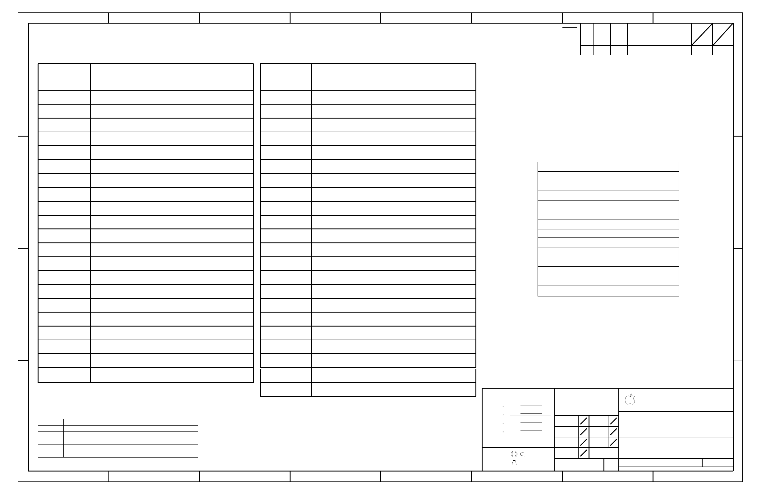
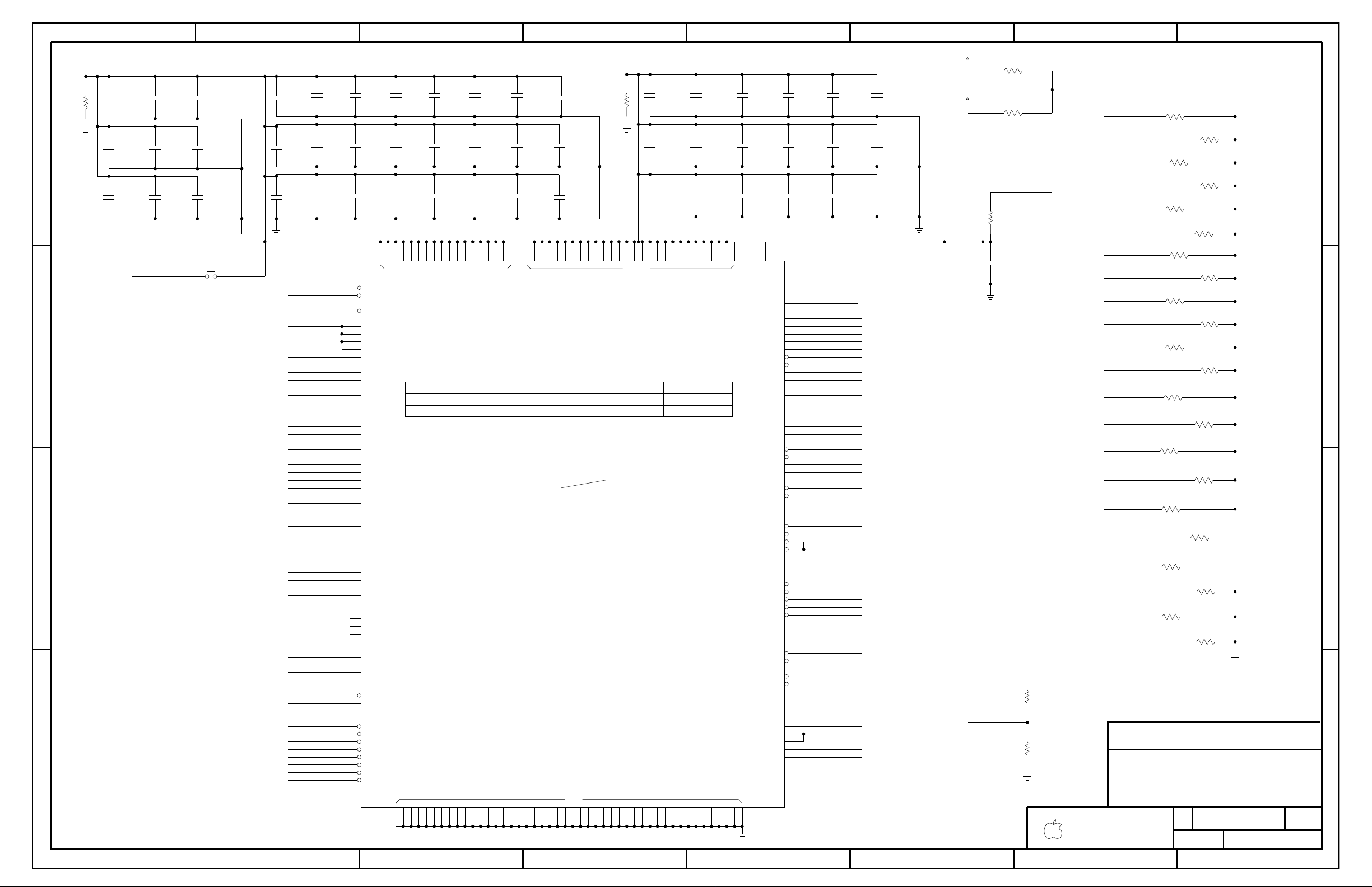
TITLE PAGE AND CONTENTS
PCB NOTES AND HOLES
SYSTEM BLOCK DIAGRAM
23
26
INTREPID MEMORY INTERFACE / BOOT ROM
GIGABIT ETHERNET INTERFACE
USB_MODEM
ATI_MEMIO_HI
OPTICAL DRIVE
41
38
External TMDS (DVI Transmitter SIL1162)
M10 AGP INTERFACE & SPREAD SPECTRUM SUPPORT
20
18
19
16
15
14
13
12
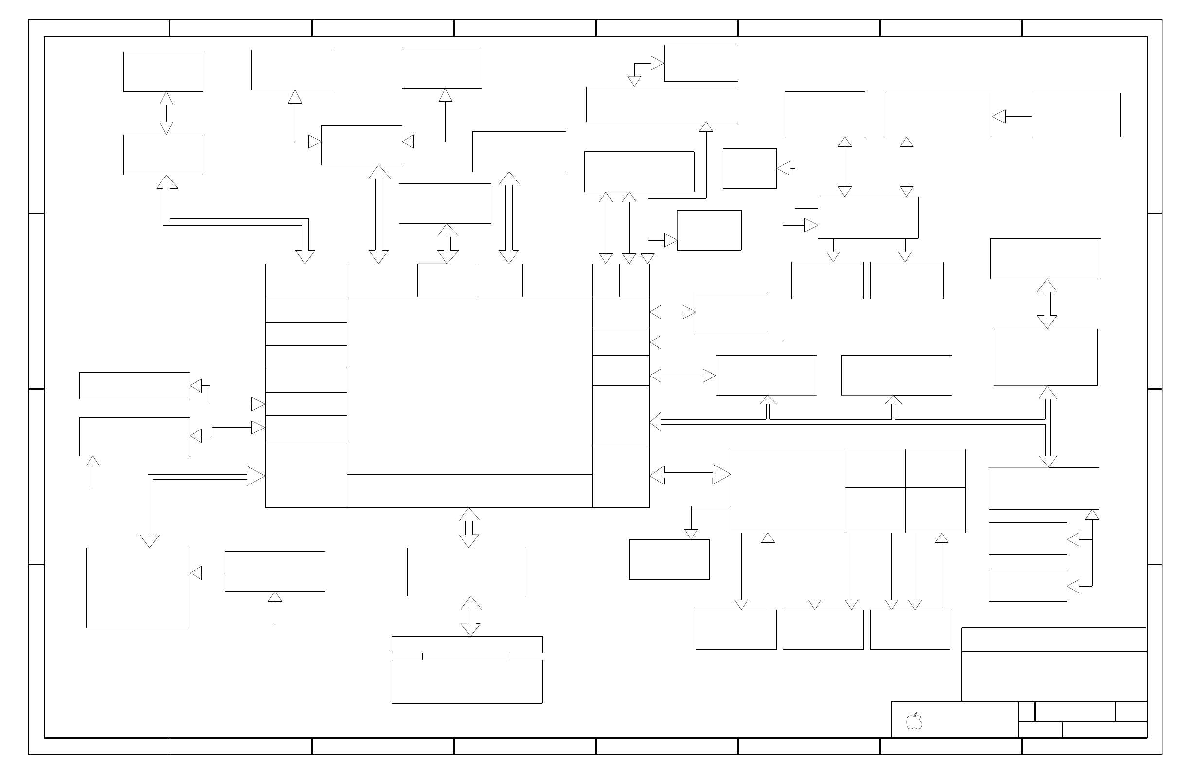
400PIN STACKED DDR SODIMM CONNECTOR
INTREPID AGP 4X/PCI
DDR MEMORY MUXES
INTREPID POWER RAILS/1.5V LDO
CARDBUS INTERFACE (PCI1510)
USB 2.0 INTERFACE (uPD720101)
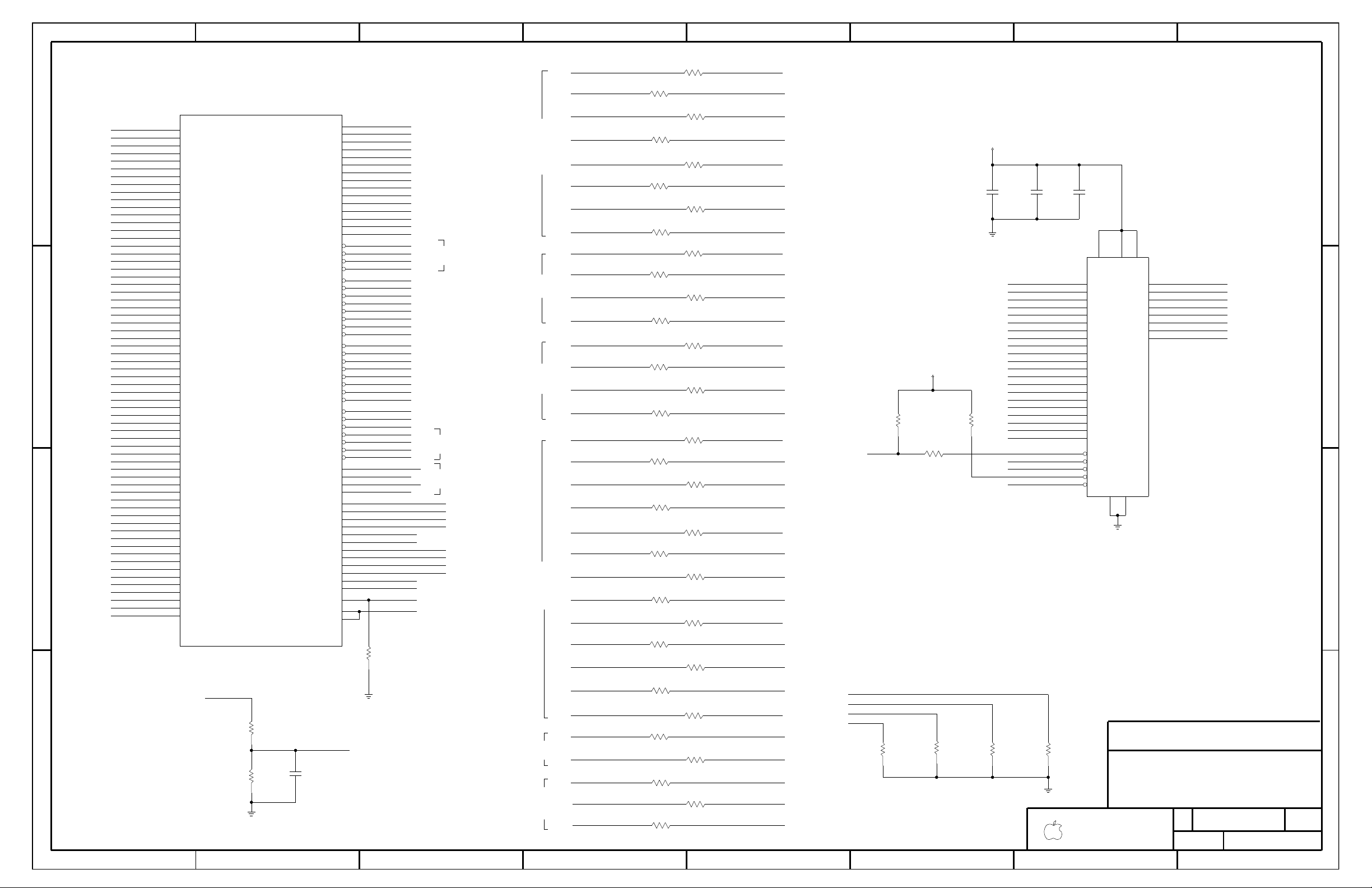
SIGNAL CONSTRAINTS (2 OF 4) - CPU
PAGE
CONTENTS
PAGE
M10 LVDS/TMDS/GPIO & GPU VCORE
INTREPID ENET/FW/UATA/EIDE INTERFACES
INTREPID DECOUPLING
INTREPID MAXBUS AND BOOT STRAPS
CPU PLL AND CONFIGURATION STRAPS
POWER BLOCK DIAGRAM
MPC7447 MAXBUS INTERFACE
SSCG
5V_HD_LOGIC
BBANG
NO_BBANG
3V_HD_LOGIC
INT_2_5V_HOT
ATI_MEMIO_LO
SOFT_MODEM
INT_2_5V_COLD
GPU_PWRMSR
GPU_SS
BOM OPTIONS (IN COMMON PARTS)
STUFF
22
INTERNAL CONNECTORS - AIRPORT, HARD DRIVE,
NO_SSCG
32
2
25
39
27
40
3
COMPONENT LOCATIONS (2 OF 2)
COMPONENT LOCATIONS (1 OF 2)
REVISION HISTORY
SIGNAL LOCATIONS
43
42
PMU
37
36
33
34
30
1
4
5
6
8
7
10
9
17
FUNCTIONAL TESTPOINTS
35
21
M10 POWER
SIGNAL CONSTRAINTS (4 OF 4) - POWER NETS
28
24
LVDS
SIGNAL CONSTRAINTS (1 OF 4) - DDR MEM/CLK
FIREWIRE PHY
29
NO STUFF
31
PBUS SUPPLY / PMU SUPPLY / BACKUP BATTERY
1_8V_MAXBUS 1_5V_MAXBUS
11
FAN CONTROLLER, USB MODEM/SOFT MODEM,
MPC7447 DATA / NC PINS / BOOTBANGER
BATTERY CHARGER AND CONNECTOR
CONTENTS
3.3V / 5V SYSTEM POWER SUPPLY
FIREWIRE PORTS
INTREPID GPIOS/SERIAL/USB INTERFACES/SSCG
VGA_BUFFER_RES
EXT_TMDS
INT_TMDS
VIDEO CONNECTORS - INVERTER, DVI, S-VIDEO,
KBD,TPAD,HALL EFFECT,PWR BUTTON,LMU/SENSOR
1.5V/ 1.8V / 2.5V SYSTEM POWER SUPPLIES
SIGNAL CONSTRAINTS (3 OF 4) - DIGITAL/DIFF
051-6338
40
?
12/05/02
02
1
ENGINEERING RELEASED
248015
C
SCHEM,MLB,PB15"
DMS630-4721
1
065-4479 DMS3
SELPRTS,MLB,PB15,BST
1
PCB1820-1441
PCBF,MLB,PB15
1
DMS1065-3951
DMS630-4285&DMS630-4721
CMNPRTS,MLB,PB15
051-6338
1
SCH1
SCHEM,MLB,PB15
SCHEM,MLB,PB15
DMS630-4285
065-3952 DMS2
1
SELPRTS,MLB,PB15,BTR
Fri Jan 23 20:30:40 2004
Page 2
D
SIZE
OF
SHT
DRAWING NUMBER
NOTICE OF PROPRIETARY PROPERTY
I TO MAINTAIN THE DOCUMENT IN CONFIDENCE
III NOT TO REVEAL OR PUBLISH IN WHOLE OR PART
II NOT TO REPRODUCE OR COPY IT
AGREES TO THE FOLLOWING
PROPERTY OF APPLE COMPUTER, INC. THE POSSESSOR
THE INFORMATION CONTAINED HEREIN IS THE PROPRIETARY
1
2
3
4
5
67
8
12
3
4
5
6
78
B
C
D
A
B
C
D
A
REV.
APPLE COMPUTER INC.
SCALE
NONE
TMDS
(VIA SIL1162)
Connector
J4
Connector
P.22
Connector
P.22P.22
2:1 DDR MUXES
64BITS
167MHZ
MEMORY BUS
2.5V
LVDS
EDID (I2C)
RGB
DDC
J22
DVI-I
PCI
MEMORY
U17
RIGHT USB
(VIA LIO)
LEFT USB
(INTERNAL MEM)
EHCI HC
NEC USB2.0
P.24
DC-In
NOT USED
NOT USED
NOT USED
BOOT ROM
(MPC7447)
P.25
3.3V/5V
16/32 BITS
33MHZ
I2C
PMU
167MHZ
1.8V
MAXBUS
32BIT ADDRESS
64BIT DATA
NOT USED
EIDE
UIDE
1394 OHCI
3.3V
50MHZ
8BIT TX/RX
P.24
P.24
@ 400MHZ
2 DATA PAIRS
P.27
PHY
FW - B
FW - A
125MHZ
8BIT RX
8BIT TX
G/MII
3.3V
10/100/1000
P.26
P.26
PHY
66MHZ
1.5V/3.3V
AGP BUS
32BITS
Connector
P.14
SCCA
I2C
P.25
Connector
Connector
Power Supply
& Charger
Connector
ULTRA ATA/100
P.18
P.22
S-VIDEO
LCD Panel
Connector
P.19-21
4X AGP
CPU
P.5-6
P.7
PCI BUS
32BITS
33MHZ
3.3V
CardBus
64MB
CH. B
CH. A
MEMORY MEMORY
I2S
CPU PLL
Config
USB PORT E
USB PORT D
10/100/1000
ETHERNET FIREWIRE
SO-DIMM Connector
DDR SDRAM DIMM 0
DDR SDRAM DIMM 1
DDR MEMORY
UATA 100
33MHZ
64BITS
CARDSLOT
VIA/PMU
SYSTEM BLOCK DIAGRAM
FireWire
USB PORT F
USB PORT C
P.25
Connector
Battery
SMBUS
3.3V
INTREPID
400 MB/S
APOLLO
Ethernet
Connector
USB PORT B
USB PORT A
@ 200MHz
Connector
P.28
INTREPID
P.28
P.13 P.13
P.13
P.14
P.14
P.14
P.14
P.14
P.14
P.8
P.9
P.10
J25
P.11
P.13 P.14
P.13
P.14
P.14
P.12
P.12
P.30
U28
P.29
P.9
Inverter
COMPOSITE
S-Video
P.30-34
P.30
U8
P.17
P.25
P.25
Fan
I2CI2S
Connector
LIO/Audio
P.25
NOT USED
EIDE
P.13
P.25
MAXBUS
(INTERNAL MEM)
Serial Debug
TI PCI1510
Controller
Connector
1M X 8
(VIA STATLER)
CH. D
(INTERNAL MEM)
MEMORY
ATI
M10
P.12
(INTERNAL MEM)
BlueTooth (LIO)
4 DATA PAIRS
Ethernet
J23
J24
U43
U36
J20
J13
J12
J3
J28
U11
J26
J27
J6
U47
J3
J17
J21J14
U16/U18/U28/U27
U56
J15
J3
U51
J5
Connector
P.18
CARDBUS
PMU
AIRPORT
CH. C
TRACKPAD
J10
P.23
SERIAL
5V
Connector
Connector
LED
J8
P.23
SLEEP
U53/J1/J18
Circuit
BOOTROM
OPTICAL DRIVE
Connector
Connector
J11
Connector
P.23
Keyboard
I2C
2 DATA PAIRS
RUX Board
LMU LUX Board
P.23
P.23
J2
J19
Modem/SW Modem
Connector
051-6338
2
40
C
Page 3
D
SIZE
OF
SHT
DRAWING NUMBER
NOTICE OF PROPRIETARY PROPERTY
I TO MAINTAIN THE DOCUMENT IN CONFIDENCE
III NOT TO REVEAL OR PUBLISH IN WHOLE OR PART
II NOT TO REPRODUCE OR COPY IT
AGREES TO THE FOLLOWING
PROPERTY OF APPLE COMPUTER, INC. THE POSSESSOR
THE INFORMATION CONTAINED HEREIN IS THE PROPRIETARY
1
2
3
4
5
67
8
12
3
4
5
6
78
B
C
D
A
B
C
D
A
REV.
APPLE COMPUTER INC.
SCALE
NONE
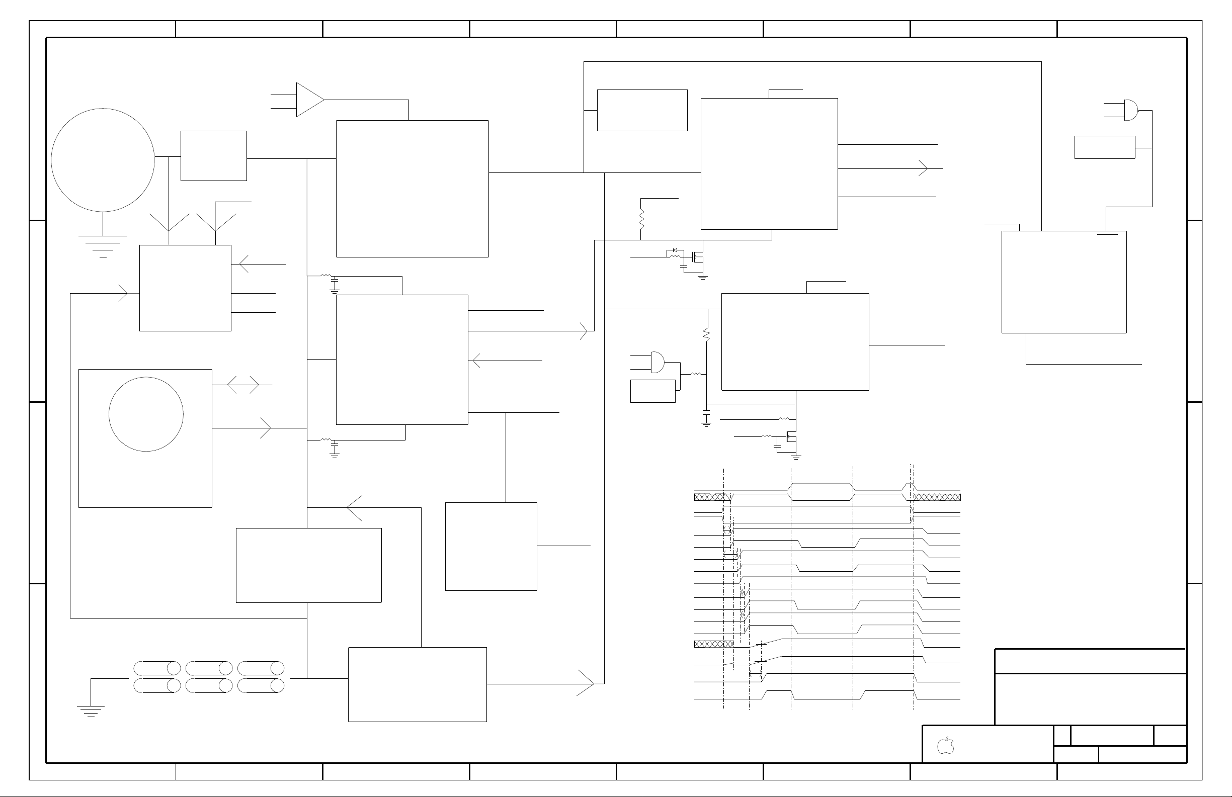
BACKUP
SLEEP: D3COLD
(+1.385V)
+1.2V
(LTC1778)
GPU_VCORE
CPU_VCORE
+3V_SLEEP
1_5V_2_5V_OK
+3V_MAIN
+2_5V_SLEEP
SLEEP_L_LS5
~2.23MS
SHUTDOWN: STOPPED
RUN: RUNNING
RUN/SS
SLEEP: RUNNING
DC/DC
(LTC3411)
SHUTDOWN: STOPPED
SLEEP: STOPPED
RUN: RUNNING
(MAX1772)
FEED-IN PATH
NO INRUSH PROTECTION
BATTERY
CHARGER
PG 30
WHEN ONLY BATTERY IS CONNECTED
+4_6V_BU
SHUTDOWN: RUNNING
AC: 12.8V
REGULATOR
(LTC1625)
MAIN 2.5V/1.5V
SHUTDOWN: STOPPED
+PBUS
INTREPID CORE
SHUT-DOWN
CHARGER INPUT
PG 20
PG 33
INTERNAL 1.2UA CURRENT SOURCE
TURNS ON AS LOW AS 0.8V/TYP 1.5V
PG 34
PG 34
PG 32
PG 31
PG 31
PG 30
PG 30
PG 30
PG 31
PG 31
NO AC: BATTERY VOLTAGE
VCC
POWER SYSTEM ARCHITECTURE
MAP31 DDR I/O
MAP31 DDR CORE
AND PREVENTS +PBUS AND +24V_PBUS FROM DROPPING BELOW 6V
BACKUP BATTERY CIRCUIT CHARGES OFF +PBUS
+PBUS
+PBUS
+PBUS
BATTERY VOLTAGE
RUN/SS
STARTS ~4.25MSEC AFTER DCDC_EN_L BECOMES LOW
RC AT 1M*0.1UF @ 24V
STARTS 2.0MSEC AFTER DCDC_EN_L BECOMES LOW
RC AT 1M*0.047UF @ 24V
INTERNAL ZENER CLAMP TO 6V
<100UA ALLOWED
TURNS ON AT >1V
RUN/SS - 5V
<100UA ALLOWED
MAIN 3V/5V
(LTC3707)
DC/DC
TURNS ON AT >1V
VCC
DCDC_EN_L
AFTER PMU IS UP AND RUNNING
DCDC_EN_L WILL PULL ON1/ON2
LOW IN SHUTDOWN
+5V_MAIN
+1.8V_MAIN
+5V_MAIN
VCC
1_5V_2_5V_OK
+BATT
+BATT
+24V_PBUS
+24V_PBUS
NO INRUSH PROTECTION
TURNS ON OUTPUT @ 2.4V
RUN: RUNNING
SHUTDOWN: STOPPED
RUN/SS - 3V
SLEEP: RUNNING
RUN: RUNNING
24V IS OUTPUT ONLY FROM
BATTERY
BACKUP BATTERY
1V20_REF
+
-
& BOOST OUTPUT
POWER BLOCK DIAGRAM
(UNTIL DRAINED)
AC
IN
ADAPTER
LIMITER
INRUSH
>~13.44V TURNS-ON
<~13.44V SHUTS-OFF
BUCK
RUN: RUNNING
+3.3V_MAIN
STBYMD
+3V_PMU
LDO
+3V_PMU
14V_PBUS
14V_PBUS
+5V_MAIN
WHEN ONLY BATTERY IS CONNECTED
14V CHARGES BACKUP BATTERY
HOLDS BOTH RUN/SS AT GND
WHEN IT’S CONNECTED TO GND
WHEN IT’S OPEN
TURNS CONTROL TO RUN/SS
INVERTER
BACKLIGHT
DC/DC
(MAX1715)
PGOOD
3V_5V_OK
PGOOD
1625 NOT RUNNING
ON1/ON2
+1.5V_MAIN
+2.5V_MAIN
DDR POWER
AGP I/O
MAXBUS
SLEEP: STOPPED
SHUTDOWN: STOPPED
RUN: RUNNING
DC/DC
(MAX1717)
+5V_MAIN
SHDN
VCC
SLEEP
DCDC_EN
MAXBUS
SEQUENCING
+5V_MAIN
DC/DC
EXT_VCC
VCC
D3_COLD
SLEEP
DCDC_EN
HOWEVER, 5V SHOULD TURN ON ~2.23MS AFTER
RC CHARGING AT INT_VCC (5V)
DCDC_EN_L OR PMU_POWERUP_L
BECOMES ’1’; MUCH LESS THAN THE
+5V_MAIN TURNS ON
1_5V_2_5V_OK WILL NOT PULL LOW UNTIL
D3_HOT
D3_HOT
1_5V_2_5V_OK
DCDC_EN_L
SEQUENCING
GPU_VCORE
~5.88MS TO START SWITCHER
1M & 0.1UF @14V, IT TAKES
DCDC_EN_L
DCDC_EN
+5V_MAIN
+5V_SLEEP
2.4V - ??? MS
3V_5V_OK
SLEEP
??? MS
+2_5V_MAIN
??? MS
+1_5V_MAIN
+1_5V_SLEEP
1_5V_2_5V_OK
(MAX1715 OUTPUT)
(AT LTC1778 RUN/SS)
GPU_VCORE
(D3HOT)
GPU_VCORE
(D3COLD)
~8.2MS
~7.36MS
SLEEP
RUN
SHUT-DOWN
RUN
3S 2P 18650 CELLS
SLEEP: RUNNING
+5V_MAIN
INTERNAL ZENER CLAMP TO 6V
C
3
40
051-6338
Page 4
D
SIZE
OF
SHT
DRAWING NUMBER
NOTICE OF PROPRIETARY PROPERTY
I TO MAINTAIN THE DOCUMENT IN CONFIDENCE
III NOT TO REVEAL OR PUBLISH IN WHOLE OR PART
II NOT TO REPRODUCE OR COPY IT
AGREES TO THE FOLLOWING
PROPERTY OF APPLE COMPUTER, INC. THE POSSESSOR
THE INFORMATION CONTAINED HEREIN IS THE PROPRIETARY
1
2
3
4
5
67
8
12
3
4
5
6
78
B
C
D
A
B
C
D
A
REV.
APPLE COMPUTER INC.
SCALE
NONE
GROUND VIAS
PCB SPECS
THICKNESS : 1.2 MM / 0.047 IN
PREPREG (3 MIL)
PREPREG (3 MIL)
CORE (3 MIL)
CORE (3 MIL)
PREPREG (3 MIL)
PREPREG (3 MIL)
PREPREG (5 MIL)
PREPREG (5 MIL)
CORE (5 MIL)
CUT POWER PLANE (1 OZ)
CUT POWER PLANE (1 OZ)
SIGNAL (1/2 OZ + COPPER PLATING)
SIGNAL (1/2 OZ + COPPER PLATING)
BOARD HOLES
BOARD INFORMATION
SEE PCB CAD FILES FOR MORE SPECIFIC INFO.
IMPEDANCE : 50 OHMS +/- 10%
1/2 OZ CU THICKNESS: 0.7 MILS
DIELECTRIC: FR-4
LAYER COUNT: 10
BOARD STACK-UP AND CONSTRUCTION
SIGNAL TRACE WIDTH: 4 MILS
PREPREG THICKNESS: 2-3 MILS
SIGNAL TRACE SPACING: 4 MILS
I/O AREA
1394
1
4
5
7
6
3
2
8
9
10
GROUND (1/2 OZ)
SIGNAL (1/2 OZ)
SIGNAL (1/2 OZ)
1-8-1 BLIND MICROVIA/20R10 BURIED VIA/20R10 TH VIA
SIGNAL (1/2 OZ)
GROUND (1/2 OZ)
SIGNAL (1/2 OZ)
1.0 OZ CU THICKNESS: 1.4 MILS
LWR CPU
UPPER RT GPU
LEFT CPU
LWR RT GPU
INVERTER
DVI
DVI
BATT. CHRGR
CHASSIS MOUNTS
ASICS HEATSINK MOUNTS
MECH. HOLES
1
ZT70
HOLE-VIA-20R10
1
ZT9
HOLE-VIA-20R10
1
ZT2
HOLE-VIA-20R10
1
ZT73
HOLE-VIA-20R10
1
ZT75
HOLE-VIA-20R10
1
ZT63
HOLE-VIA-20R10
1
ZT77
HOLE-VIA-20R10
1
ZT66
HOLE-VIA-20R10
1
ZT65
HOLE-VIA-20R10
1
ZT62
HOLE-VIA-20R10
1
ZT25
HOLE-VIA-20R10
1
ZT24
HOLE-VIA-20R10
1
ZT19
HOLE-VIA-20R10
1
ZT67
HOLE-VIA-20R10
1
ZT37
HOLE-VIA-20R10
1
ZT29
HOLE-VIA-20R10
1
ZT31
HOLE-VIA-20R10
1
ZT1
HOLE-VIA-20R10
1
ZT12
HOLE-VIA-20R10
1
ZT14
HOLE-VIA-20R10
1
ZT27
HOLE-VIA-20R10
1
ZT26
HOLE-VIA-20R10
1
ZT13
HOLE-VIA-20R10
1
ZT30
HOLE-VIA-20R10
1
ZT33
HOLE-VIA-20R10
1
ZT18
HOLE-VIA-20R10
3
2
1
SH1
SHLD-SM
OG-503040
CHGND5
1
ZT7
HOLE-VIA-20R10
1
ZT21
HOLE-VIA-20R10
1
ZT59
HOLE-VIA-20R10
1
ZT58
HOLE-VIA-20R10
1
ZT85
HOLE-VIA-20R10
1
ZT86
HOLE-VIA-20R10
1
ZT16
HOLE-VIA-20R10
1
ZT74
HOLE-VIA-20R10
1
ZT36
HOLE-VIA-20R10
1
ZT23
HOLE-VIA-20R10
1
ZT42
HOLE-VIA-20R10
CHGND2
CHGND1
CHGND3
1
ZT76
HOLE-VIA-20R10
1
ZT41
HOLE-VIA-20R10
1
ZT40
HOLE-VIA-20R10
1
ZT39
HOLE-VIA-20R10
1
ZT38
HOLE-VIA-20R10
1
ZT61
HOLE-VIA-20R10
1
ZT64
HOLE-VIA-20R10
1
ZT68
HOLE-VIA-20R10
1
ZT69
HOLE-VIA-20R10
1
ZT72
HOLE-VIA-20R10
1
ZT28
HOLE-VIA-20R10
1
ZT46
HOLE-VIA-20R10
1
ZT71
HOLE-VIA-20R10
1
ZT78
HOLE-VIA-20R10
1
ZT80
HOLE-VIA-20R10
1
ZT51
HOLE-VIA-20R10
1
ZT50
HOLE-VIA-20R10
1
ZT52
HOLE-VIA-20R10
1
ZT53
HOLE-VIA-20R10
1
ZT57
HOLE-VIA-20R10
1
ZT82
HOLE-VIA-20R10
1
ZT60
HOLE-VIA-20R10
1
ZT22
HOLE-VIA-20R10
1
ZT17
HOLE-VIA-20R10
1
ZT35
HOLE-VIA-20R10
1
ZT45
HOLE-VIA-20R10
1
ZT79
HOLE-VIA-20R10
1
ZT83
HOLE-VIA-20R10
1
ZT81
HOLE-VIA-20R10
1
ZT49
HOLE-VIA-20R10
1
ZT47
HOLE-VIA-20R10
1
ZT48
HOLE-VIA-20R10
1
ZT54
HOLE-VIA-20R10
1
ZT55
HOLE-VIA-20R10
1
ZT56
HOLE-VIA-20R10
1
ZT5
HOLE-VIA-20R10
1
ZT84
HOLE-VIA-20R10
1
ZT15
HOLE-VIA-20R10
1
ZT44
HOLE-VIA-20R10
1
ZT4
HOLE-VIA-20R10
1
ZT8
HOLE-VIA-20R10
1
ZT6
HOLE-VIA-20R10
1
ZT3
HOLE-VIA-20R10
1
ZT32
HOLE-VIA-20R10
1
ZT10
HOLE-VIA-20R10
1
ZT34
HOLE-VIA-20R10
1
ZT11
HOLE-VIA-20R10
1
ZT20
HOLE-VIA-20R10
1
ZT43
HOLE-VIA-20R10
C
40
4
051-6338
ZT10_SPN
NO_TEST=TRUE
ZT302_SPN
NO_TEST=TRUE
NO_TEST=TRUE
ZT301_SPN
Page 5
(1 OF 3)
TEST4
TEST3
TEST2
TEST1
TEST0
EXT_QUAL
TBEN
L2TSTCLK
L1TSTCLK
TCK
TMS
TDO
TDI
DTI0
DTI1
DTI2
DTI3
PLL_EXT
PLLCFG3
PLLCFG2
PLLCFG1
PLLCFG0
CLKOUT
SYSCLK
BVSEL
TT3
TT2
TT1
TSIZ0
TSIZ2
TSIZ1
TT4
TT0
A33
A34
A35
AP0
AP3
AP2
AP4
AP1
A25
A24
A23
A26
A27
A28
A29
A30
A31
A32
A13
A14
A15
A16
A17
A18
A19
A20
A21
A22
A12
A10
A9
A8
A7
A6
A3
A4
A5
A11
A2
A0
A1
OVDD
VDD
GND
AVDD
BR*
BG*
TS*
TRST*
LSSDMODE*
TA*
TEA*
QREQ*
QACK*
CKSTP_IN*
CKSTP_OUT*
INT*
SMI*
MCP*
SRESET*
HRESET*
PMON_IN*
PMON_OUT*
BMODE0*
BMODE1*
TBST*
GBL*
WT*
CI*
AACK*
ARTRY*
SHD0*
HIT*
SHD1*
DRDY*
DBG*
TABLE_5_ITEM
TABLE_5_ITEM
CRITICAL BOM OPTION
TABLE_5_HEAD
PART#
DESCRIPTION
QTY
REFERENCE DESIGNATOR(S)
D
SIZE
OF
SHT
DRAWING NUMBER
NOTICE OF PROPRIETARY PROPERTY
I TO MAINTAIN THE DOCUMENT IN CONFIDENCE
III NOT TO REVEAL OR PUBLISH IN WHOLE OR PART
II NOT TO REPRODUCE OR COPY IT
AGREES TO THE FOLLOWING
PROPERTY OF APPLE COMPUTER, INC. THE POSSESSOR
THE INFORMATION CONTAINED HEREIN IS THE PROPRIETARY
1
2
3
4
5
67
8
12
3
4
5
6
78
B
C
D
A
B
C
D
A
REV.
APPLE COMPUTER INC.
SCALE
NONE
MORE 0805 10UF CAPS ON VCORE POWER SUPPLY PAGE (PG 32)
CPU_VCORE DECOUPLING NETWORK
NC
470OHM FOR BOOT BANGER
NC
NC
NC
NC
NC
NC
470OHM FOR BOOT BANGER
470OHM FOR BOOT BANGER
MPC7447 PULL-UPS
MPC7447 MAXBUS
CPU_OVDD DECOUPLING NETWORK
MPC7447
CPU INTERNAL PLL FILTERING
21
R46
10K
5%
1/16W
MF
402
21
R13
5%
1/16W
MF
402
10K
21
R20
402
MF
1/16W
5%
10K
21
R32
470
5%
1/16W
MF
402
21
R11
5%
1/16W
MF
402
10K
2
1
R10
NO_BBANG
402
200
5%
1/16W
MF
21
R4
402
MF
1/16W
10K
5%
21
R7
1K
1/16W
MF
402
5%
21
R24
1/16W
MF
402
5%
10K
21
R34
10K
1/16W
MF
402
5%
2
1
C89
0.1uF
20%
CERM
402
10V
2
1
C73
0.1uF
402
10V
20%
CERM
2
1
C18
0.1uF
20%
CERM
402
10V
2
1
C20
0.1uF
10V
402
CERM
20%
2
1
C75
0.1uF
CERM
20%
402
10V
2
1
C9
0.1uF
CERM
20%
10V
402
2
1
C49
0.1uF
402
10V
CERM
20%
2
1
C46
0.1uF
CERM
402
10V
20%
2
1
C30
0.1uF
20%
CERM
10V
402
2
1
C56
0.1uF
20%
10V
402
CERM
2
1
C45
0.1uF
20%
CERM
10V
402
2
1
C48
0.1uF
CERM
402
10V
20%
2
1
C44
0.1uF
10V
402
CERM
20%
2
1
C86
0.1uF
402
10V
20%
CERM
2
1
C88
0.1uF
10V
402
CERM
20%
2
1
C10
0.1uF
402
10V
20%
CERM
2
1
C38
0.1uF
20%
CERM
402
10V
2
1
C72
0.1uF
402
10V
20%
CERM
2
1
R89
MF
5%
470
1/16W
402
2
1
C50
0.1uF
402
10V
CERM
20%
2
1
C28
0.1uF
20%
10V
402
CERM
2
1
C39
0.1uF
402
CERM
20%
10V
2
1
C47
0.1uF
CERM
402
10V
20%
2
1
C26
0.1uF
20%
CERM
10V
402
2
1
C31
0.1uF
20%
10V
402
CERM
2
1
R38
470
5%
1/16W
MF
402
21
R36
5%
1/16W
MF
402
10K
21
R45
470
5%
1/16W
MF
402
21
R28
5%
10K
402
1/16W
MF
21
R3
5%
402
MF
1/16W
1K
C32
10uF
805
CERM
6.3V
20%
2
1
C33
10uF
805
CERM
20%
6.3V
C59
805
CERM
6.3V
20%
10uF
2
1
C58
6.3V
20%
CERM
805
10uF
21
R27
MF
5%
1/16W
402
10K
21
R33
402
1/16W
MF
5%
10K
1
2
R748
1/16W
MF
402
402
1%
2
1
C62
2.2uF
10V
805
CERM
20%
2
1
C34
2.2uF
20%
805
10V
CERM
21
R25
5%
10K
1/16W
MF
402
21
R8
5%
10K
1/16W
MF
402
21
R281
1_5V_MAXBUS
603
MF
1/16W
5%
0
21
R283
1_8V_MAXBUS
603
MF
1/16W
5%
0
+1_5V_SLEEP
+1_8V_SLEEP
2
1
R9
1/16W
470
5%
MF
402
BBANG
21
R2
402
MF
1/16W
5%
470
D3
K10
K8
J13
J11
J9J7H12
H10
M12
M10
M8
L13
L11
L9L7K14
K12
H8
C5
E9
F6
E6
E5
E7
F7
G6
L4
A5
F1
D10
E10
B10
B6
A12
L1
A4
B9
C6
F11
E1
K6
A10
A2
F9
H5
E4
P4
G5
A9
D9
A7
D7
C7
C8
B8
J5H3G18
F2
E18
D5
C12
V14
V10
V7V4U16
U12
U2T9T6C2R16
R13
R4
P11
P8P2N6M3L5
K2
B4
C9
E8
B3
G8
D4
D8
B2
H7
H4
G17
F3
E17
V15
V11
V8
V5
U17
U13
U3
D13
T10
T7
R17
R14
R5
P12
P9P3N7
M13D6M11
M9M7M4
L12
L10
L8
L6
K13
K11
C3
K9K3K7
J12
J10
J8
J6
H13
H11
H9
B5
E2
A11
N1
P1
K1
G1
R3
M2
H2
B1
A3
J1
B7D2
F8
G9
M1
A8
N2
G7
F5
H6
E3
C1
R1
G2
C10
D1
D11
L2
F10
B11
G10
C4
B12
W1
N5
G3
U1
V2
T1
N3
P5
M5
J3
N4
K4
J2
C11
W2
K5
R2
J4
V1
F4
T2
G4
L3
D12
H1
E11
U56
800MHZ
BGA
APOLLO_MPC7445_360
OMIT
2
1
C29
0.1uF
20%
CERM
10V
402
2
1
C27
0.1uF
402
10V
CERM
20%
2
1
C25
0.1uF
20%
CERM
10V
402
2
1
C54
0.1uF
20%
CERM
10V
402
2
1
C53
0.1uF
20%
CERM
10V
402
2
1
C55
0.1uF
20%
CERM
10V
402
2
1
C87
0.1uF
20%
CERM
402
10V
2
1
C69
0.1uF
10V
402
CERM
20%
2
1
C17
0.1uF
20%
CERM
402
10V
2
1
C82
0.1uF
10V
402
CERM
20%
2
1
C81
0.1uF
20%
CERM
402
10V
2
1
C61
0.1uF
10V
402
20%
CERM
21
R6
5%
1/16W
MF
402
10K
21
R37
5%
1/16W
MF
402
10K
21
R19
5%
1/16W
MF
402
10K
21
R26
5%
1/16W
MF
402
10K
2
1
C2
0.1uF
20%
CERM
10V
402
2
1
C103
0.1uF
20%
CERM
10V
402
2
1
C68
0.1uF
20%
CERM
10V
402
2
1
C109
20%
CERM
10V
0.1uF
402
2
1
C107
CERM
20%
0.1uF
10V
402
2
1
C104
10uF
805
CERM
20%
6.3V
2
1
C108
0.1uF
402
10V
CERM
20%
2
1
C110
0.1uF
20%
CERM
10V
402
2
1
C1
0.1uF
20%
CERM
10V
402
21
XW34
SM
OMIT
2
1
C810
402
10V
20%
CERM
0.1uF
2
1
C811
805
CERM
20%
10V
2.2uF
1
CRITICAL
CPU_BTR
337S2732
U56
IC,APOLLO7,1.x,1.0GHZ,1.XV CORE,85C
U56
CPU_BST
1
CRITICAL
IC,APOLLO7,1.X,1.25GHZ,1.XV CORE,85C
337S2748
40
5
051-6338
C
CPU_SHD1_L
MAXBUS_SLEEP
CPU_AVDD
CPU_DRDY_L
CPU_EDTI
MAXBUS_SLEEP
CPU_PULLDOWN
CPU_PULLDOWN
CPU_SRWX_L
JTAG_CPU_TDI
CPU_LSSD_MODE
CPU_PULLDOWN
JTAG_CPU_TCK
CPU_EDTI
JTAG_CPU_TMS
CPU_L1TSTCLK
MPIC_CPU_INT_L
CPU_SRESET_L
CPU_SMI_L
CPU_HRESET_L
CPU_EMODE1_L
CPU_PULLUP
CPU_PMONIN_L
CPU_SRWX_L
CPU_CHKSTP_OUT_L
CPU_MCP_L
CPU_SHD0_L
CPU_TBEN
CPU_CHKS_L
CPU_TT<0>
CPU_BR_L
CPU_TS_L
CPU_ADDR<2>
CPU_ADDR<0>
CPU_ADDR<1>
CPU_ADDR<3>
CPU_ADDR<4>
CPU_ADDR<5>
CPU_ADDR<6>
CPU_ADDR<7>
CPU_ADDR<10>
CPU_ADDR<9>
CPU_ADDR<8>
CPU_ADDR<12>
CPU_ADDR<11>
CPU_ADDR<15>
CPU_ADDR<14>
CPU_ADDR<13>
CPU_ADDR<17>
CPU_ADDR<16>
CPU_ADDR<20>
CPU_ADDR<19>
CPU_ADDR<18>
CPU_ADDR<22>
CPU_ADDR<21>
CPU_ADDR<25>
CPU_ADDR<23>
CPU_ADDR<24>
CPU_ADDR<27>
CPU_ADDR<26>
CPU_ADDR<28>
CPU_ADDR<29>
CPU_ADDR<30>
CPU_ADDR<31>
CPU_TT<1>
CPU_TT<4>
CPU_TT<3>
CPU_TT<2>
CPU_TSIZ<0>
CPU_TBST_L
CPU_TSIZ<1>
CPU_GBL_L
CPU_TSIZ<2>
CPU_AACK_L
CPU_WT_L
CPU_CI_L
CPU_ARTRY_L
CPU_SHD0_L
CPU_SHD1_L
CPU_HIT_L
MAXBUS_SLEEP
JTAG_CPU_TRST_L
CPU_PLL_CFG<0>
CPU_PLL_CFG<1>
SYSCLK_CPU
CPU_CLKOUT_SPN
NO_TEST=TRUE
CPU_PLL_CFG<4>
CPU_PLL_CFG<2>
CPU_DTI<2>
CPU_DTI<0>
CPU_DTI<1>
CPU_DBG_L
CPU_PLL_CFG<3>
CPU_L2TSTCLK
CPU_LSSD_MODE
CPU_L1TSTCLK
JTAG_CPU_TMS
JTAG_CPU_TRST_L
JTAG_CPU_TCK
JTAG_CPU_TDO_TP
JTAG_CPU_TDI
CPU_QACK_L
CPU_QREQ_L
CPU_TBEN
CPU_TEA_L
CPU_SRESET_L
CPU_HRESET_L
CPU_SMI_L
CPU_MCP_L
MPIC_CPU_INT_L
CPU_CHKSTP_OUT_L
CPU_PMONIN_L
CPU_EMODE0_L
CPU_EMODE1_L
CPU_CHKS_L
CPU_PULLUP
CPU_BUS_VSEL
CPU_L2TSTCLK
CPU_VCORE_SLEEP
ADT7460_VCORE_MON
CPU_VCORE_SLEEP
CPU_PULLDOWN
CPU_TA_L
CPU_BG_L
38
38
38
33
33
33
16
16
16
15
15
15
8
8
39
8
39
39
39
7
7
39
39
39
7
7
39
39
39
39
39
7
38
38
6
36
6
6
6
6
14
39
29
6
39
8
36
36
36
36
36
36
36
36
36
36
36
36
36
36
36
36
36
36
36
36
36
36
36
36
36
36
36
36
36
36
36
36
36
36
36
36
36
36
36
36
36
36
36
36
36
36
36
36
36
6
6
35
36
36
36
36
6
6
6
6
36
36
8
36
39
6
29
14
39
33
33
36
36
5
5
38
8
5
5
5
5
5
5
5
5
5
5
5
5
5
5
5
5
5
5
5
5
5
5
5
5
5
8
8
8
8
8
8
8
8
8
8
8
8
8
8
8
8
8
8
8
8
8
8
8
8
8
8
8
8
8
8
8
8
8
8
8
8
8
8
8
8
8
8
8
8
8
8
8
8
5
5
8
5
5
7
7
8
7
7
8
8
8
8
7
5
5
5
5
5
5
39
5
8
8
5
8
5
5
5
5
5
5
5
7
5
5
5
7
5
5
25
5
5
8
8
Page 6
(2 OF 3)
D0
D60
D61
D62
D63
DP7
DP0
DP1
DP2
DP3
DP4
DP5
DP6
D59
D56
D57
D58
D55
D54
D53
D52
D50
D51
D49
D46
D45
D47
D48
D44
D43
D42
D41
D40
D39
D38
D37
D36
D35
D34
D33
D30
D31
D32
D29
D26
D25
D24
D23
D27
D28
D22
D21
D20
D19
D18
D17
D16
D15
D14
D13
D12
D11
D10
D9
D8
D7
D6
D5
D4
D1
D2
D3
(3 OF 3)
NC_B14
NC_B13
NC_E12
NC_B18
NC_N19
NC_K17
NC_N18
NC_N12
NC_A6
NC_C13
NC_G11
NC_A14
NC_F12
NC_A13
NC_A18
NC_C14
NC_A15
NC_B16
NC_E13
NC_F13
NC_F14
NC_G12
NC_A17
NC_C15
NC_G14
NC_H14
NC_E14
NC_G13
NC_C16
NC_C17
NC_B17
NC_B15
NC_E15
NC_D14
NC_A19
NC_B19
NC_A16
NC_C18
NC_G15
NC_D15
NC_C19
NC_K16
NC_J17
NC_K18
NC_L18
NC_L19
NC_M18
NC_P16
NC_L16
NC_H15
NC_J16
NC_K19
NC_J15
NC_J19
NC_J18
NC_J14
NC_K15
NC_L14
NC_L17
NC_M15
NC_N17
NC_P19
NC_M16
NC_M19
NC_N16
NC_N13
NC_M17
NC_M14
NC_N14
NC_P18
NC_N15
NC_D19
NC_F15
NC_G19
NC_E16
NC_D17
NC_D16
NC_P15
NC_L15
NC_H19
NC_H18
NC_H17
NC_H16
NC_E19
NC_D18
NC_F16
NC_G16
NC_F19
NC_F17
NC_F18
VCC
RESET*
XTAL1
XTAL2
PB0
PD6
PD5
PD4
PD3
PD2
PD1
PD0
GND
PB1
PB2
PB3
PB4
PB5
PB6
PB7
SYM_VER2
WC*
VCC
VSS
SDA
SCL
NC1
NC2
NC3
Y
B
A
Y
B
A
D
SIZE
OF
SHT
DRAWING NUMBER
NOTICE OF PROPRIETARY PROPERTY
I TO MAINTAIN THE DOCUMENT IN CONFIDENCE
III NOT TO REVEAL OR PUBLISH IN WHOLE OR PART
II NOT TO REPRODUCE OR COPY IT
AGREES TO THE FOLLOWING
PROPERTY OF APPLE COMPUTER, INC. THE POSSESSOR
THE INFORMATION CONTAINED HEREIN IS THE PROPRIETARY
1
2
3
4
5
67
8
12
3
4
5
6
78
B
C
D
A
B
C
D
A
REV.
APPLE COMPUTER INC.
SCALE
NONE
REFERENCE DESIGNATOR(S)
BOM OPTION
TABLE_5_HEAD
QTY
DESCRIPTION
PART#
TABLE_5_ITEM
NC
NC
UNSTUFFING Ra AND STUFFING Rb
WILL DISABLE THE CONTROLLER
MPC7447/BBANG
NC
NC
NC
NC
NC
NC
NC
NC
NC
NC
NC
NC
NC
NC
NC
NC
NC
NC
NC
NC
NC
NC
NC
NC
NC
NC
NC
NC
NC
NC
NC
NC
NC
NC
NC
NC
NC
NC
NC
NC
NC
NC
NC
NC
NC
NC
NC
NC
NC
NC
NC
NC
NC
NC
NC
NC
NC
NC
NC
NC
NC
NC
NC
NC
NC
NC
NC
NC
NC
NC
NC
NC
NC
NC
NC
NC
NC
NC
NC
NC
NC
NC
NC
NC
NC
NC
NC
NC
NC
NC
NC
NC
NC
NC
NC
NC
009-6240 FW GT4 BBANGER
INPUTS ARE 3V TOLERANT
INPUTS ARE 3V TOLERANT
BOOT BANGER - TWEAK PROCESSOR BITS AFTER POWER-ON
(Rb)
(Ra)
W6
N8
V3
M6
W9
T4
W4
T3
W13
V13
P14
T8
W8
R8
P6
U15
R7
U7
U8
U4
V17
W3
T17
T18
T16
W18
T15
W17
U18
W19
U19
T19
V19
R18
V18
R19
P17
W16
V6
P7
R6
W7
U5
T5
U6
W5
V9
U9
V16
W10
R9
U10
P10
N9
R10
T11
W11
U11
R11
T14
N10
N11
V12
W12
T12
R12
W14
U14
P13
T13
W15
R15
U56
OMIT
BGA
APOLLO_MPC7445_360
800MHZ
P19
P18
P16
P15
N19
N18
N17
N16
N15
N14
N13
N12
M19
M18
M17
M16
M15
M14
L19
L18
L17
L16
L15
L14
K19
K18
K17
K16
K15
J19
J18
J17
J16
J15
J14
H19
H18
H17
H16
H15
H14
G19
G16
G15
G14
G13
G12
G11
F19
F18
F17
F16
F15
F14
F13
F12
E19
E16
E15
E14
E13
E12
D19
D18
D17
D16
D15
D14
C19
C18
C17
C16
C15
C14
C13
B19
B18
B17
B16
B15
B14
B13
A6
A19
A18
A17
A16
A15
A14
A13
U56
800MHZ
BGA
OMIT
APOLLO_MPC7445_360
+3V_SLEEP
9
8
7
6
4
3
2
1
10
5
RP46
SM
25V
1/32W
5%
10K
BBANG
2
1
C762
BBANG
20%
10V
CERM
402
0.1uF
2
1
R692
10K
1%
1/16W
MF
603
BBANG
2
1
R709
NO STUFF
10K
1%
1/16W
MF
603
2
1
R707
BBANG
603
MF
1/16W
1%
10K
2
1
R712
10K
1%
1/16W
MF
603
BBANG
+3V_SLEEP
4
5
20
1
11
9
8
7
6
3
2
19
18
17
16
15
14
13
12
10
U54
OMIT
SSOP
AT90S1200A
2
1
C120
BBANG
CERM
10V
20%
402
0.1uF
+3V_SLEEP
7
4
8
5
6
3
2
1
U52
BBANG
SOI
32KX8_M24256B
2
1
R100
BBANG
402
MF
1/16W
5%
10K
4
5
3
2
1
U9
SN74AUC1G08
SC70-5
BBANG
21
R104
402
MF
1/16W
5%
0
NO_BBANG
+3V_SLEEP
2
1
R103
BBANG
402
MF
1/16W
5%
10K
4
5
3
2
1
U10
SN74AUC1G08
SC70-5
BBANG
2
1
R105
10K
5%
1/16W
MF
402
BBANG
2
1
R637
BBANG
603
MF
1/16W
1%
10K
C
051-6338
40
6
U54
BBANG
1
341S1135
MCU,PROGRAMMED W/ BBANGER
PMU_CPU_HRESET_L
BFR_TDO
INT_I2C_DATA0
BBANG_HRESET_L
PMU_CPU_HRESET_L
ICT_TRST_L
BFR_TDO
ESP_EN_L
BBANG_JTAG_TCK
BB_MOSI
BB_MISO
BB_SCK
BB_EEPR_ADDR
JTAG_CPU_TCK
BBANG_JTAG_TCK
BBANG_TCK_EN
MAXBUS_SLEEP
RESET_VREF
BB_RESET_L
BB_XTAL1_SPN
ESP_EN_L
BBANG_JTAG_TCK
JTAG_CPU_TDI
BBANG_HRESET_L
INT_I2C_CLK0
BB_MOSI
BB_SCK
BB_EEPR_WP_PD
INT_I2C_CLK0
INT_I2C_DATA0
BB_EEPR_ADDR
CPU_DATA<0>
CPU_DATA<2>
CPU_DATA<1>
CPU_DATA<3>
CPU_DATA<5>
CPU_DATA<4>
CPU_DATA<6>
CPU_DATA<7>
CPU_DATA<8>
CPU_DATA<10>
CPU_DATA<9>
CPU_DATA<12>
CPU_DATA<11>
CPU_DATA<13>
CPU_DATA<15>
CPU_DATA<14>
CPU_DATA<17>
CPU_DATA<16>
CPU_DATA<18>
CPU_DATA<19>
CPU_DATA<20>
CPU_DATA<21>
CPU_DATA<22>
CPU_DATA<23>
CPU_DATA<24>
CPU_DATA<25>
CPU_DATA<26>
CPU_DATA<27>
CPU_DATA<28>
CPU_DATA<29>
CPU_DATA<30>
CPU_DATA<31>
CPU_DATA<33>
CPU_DATA<32>
CPU_DATA<34>
CPU_DATA<35>
CPU_DATA<36>
CPU_DATA<37>
CPU_DATA<38>
CPU_DATA<40>
CPU_DATA<41>
CPU_DATA<42>
CPU_DATA<43>
CPU_DATA<44>
CPU_DATA<46>
CPU_DATA<45>
CPU_DATA<47>
CPU_DATA<48>
CPU_DATA<49>
CPU_DATA<51>
CPU_DATA<50>
CPU_DATA<52>
CPU_DATA<53>
CPU_DATA<54>
CPU_DATA<56>
CPU_DATA<55>
CPU_DATA<57>
CPU_DATA<58>
CPU_DATA<59>
CPU_DATA<61>
CPU_DATA<60>
CPU_DATA<62>
CPU_DATA<63>
ICT_TRST_L
CPU_HRESET_L
MAXBUS_SLEEP
BB_MISO
JTAG_CPU_TMS
JTAG_CPU_TRST_L
CPU_DATA<39>
38
38
33
33
16
16
39
15
39
39
39
15
23
8
23
23
23
8
39
13
39
7
13
13
13
39
7
29
11
29 39
6
39
11
11
11
36
36
36
36
36
36
36
36
36
36
36
36
36
36
36
36
36
36
36
36
36
36
36
36
36
36
36
36
36
36
36
36
36
36
36
36
36
36
36
36
36
36
36
36
36
36
36
36
36
36
36
36
36
36
36
36
36
36
36
36
36
36
36
7
6
39
39
36
6
6
6
6
6
6
6
6
6
6
6
6
6
5
6
5
39
6
6
5
6
6
6
6
6
6 6
8
8
8
8
8
8
8
8
8
8
8
8
8
8
8
8
8
8
8
8
8
8
8
8
8
8
8
8
8
8
8
8
8
8
8
8
8
8
8
8
8
8
8
8
8
8
8
8
8
8
8
8
8
8
8
8
8
8
8
8
8
8
8
6
5
5
6
5
5
8
Page 7
G
D
S
G
D
S
04
G
D
S
G
D
S
S
D
G
D
SIZE
OF
SHT
DRAWING NUMBER
NOTICE OF PROPRIETARY PROPERTY
I TO MAINTAIN THE DOCUMENT IN CONFIDENCE
III NOT TO REVEAL OR PUBLISH IN WHOLE OR PART
II NOT TO REPRODUCE OR COPY IT
AGREES TO THE FOLLOWING
PROPERTY OF APPLE COMPUTER, INC. THE POSSESSOR
THE INFORMATION CONTAINED HEREIN IS THE PROPRIETARY
1
2
3
4
5
67
8
12
3
4
5
6
78
B
C
D
A
B
C
D
A
REV.
APPLE COMPUTER INC.
SCALE
NONE
MULTIPLIER
R10D
STATE ENCODING CPU_PLL_STOP_OC CPU_VCORE_HI_OC
CPU CONFIGURATION
+5V_SLEEP NOW REQUIRED FOR PLL_STOP_L
PULLUP TO ENSURE THAT Vgs OF PASS
TRANSISTOR ON CPU_PLL_CFG<4> IS MET.
R10AR00A
MAXBUS VSEL
1.5V INTERFACE
INVERTED HRESET_L
BUSTYPE SELECT
APOLLO ONLY SUPPORTS MAXBUS
(PROCESSOR)
CPU_BUS_VSEL
SIGNAL
(PROCESSOR)
CPU_EMODE0_L
CPU_HRESET_L
CPU_HRESET_INV
CPU_HRESET_L
TIED
HIGH
LOW
1.8V INTERFACE
1.5V INTERFACE
2.5V INTERFACE
60X BUS MODE
APPLICATION
MAX BUS MODE
DESKTOP HAD PROBLEM USING
INVERTER TO INVERT HRESET_L
NEED TO CHARACTERIZE
1.8V INTERFACE
933
267
400
533
867
800
733
667
0 1011 0B
0 1001 09
917
8335.0X
5.5X
333
500
667
9.5X
8.5X
8.0X
9.0X
7.5X
7.0X
6.5X
6.0X
4.0X
3.0X
2.0X
1.0X
0.0X
APOLLO 7
R10E R00ER01A
PLL DISABLE 1 X
HIGH SPEED 0 1
R01B R10B R00C R10C R00DR01D
LOW SPEED 0 0
R01E
CPU FREQUENCY CONFIGURATION
(MHZ)
PLL OFF
133MHZ
(Bus-to-Core)
0 1111 0F
CPU_PLL_CFG
(AT BUS FREQUENCY)
CORE FREQUENCY
167MHZ
PLL BYPASS 0 0011 03
0 0100 04
0 1000 08
0 1010 0A
0 1101 0D
0 0101 05
0 0010 02
0 1100 0C
0 0001 01
1000
1067
1000
1083
1167
1250
1333
1 0110 16
32004000
3733466728.0X
24.0X
1 1010 1A
0 0000 00
1 1000 18
1 1001 19
1833
1667
1750
1917
1467
1333
1400
1533
1 1100 1C
1 0001 11
1 1101 1D
1 0101 15
0 1110 0E
1 0000 10
1 0010 12
1 0011 13
1 1011 1B
1 1111 1F
1 0100 14
1667
1600
2667
2400
2267
1800
1733
2133
2000
18672333
2500
2667
2083
2000
3333
3000
2833
2250
2167
3500 2800
16.0X
15.0X
14.0X
10.0X
10.5X
11.0X
12.0X
11.5X
12.5X
13.0X
13.5X
17.0X
18.0X
20.0X
21.0X
1 0111 17
12001500
1417 1133
0 0110 06
1583 1267
0 0111 07
1 1110 1E
CPU CONFIGURATION
4 0123
E ABCD HEX
R10E, R01E, OR PULLUP STUFFED
STUFF PASS TRANSISTOR ONLY IF
CPU PLL CONFIG CIRCUITRY
R00B R01C
2
1
R63
402
MF
0
1/16W
5%
CPU_BST
2
1
R92
NO STUFF
402
MF
1/16W
5%
0
2
1
R35
1/16W
5%
MF
402
10K
2
1
R50
402
MF
1/16W
5%
10K
2
1
R68
10K
5%
1/16W
MF
402
2
1
R79
402
MF
1/16W
5%
10K
2
1
R133
402
5%
1/16W
MF
47K
2
1
R132
402
5%
1/16W
MF
10K
2
1
R14
82K
402
MF
1/16W
5%
2
1
R31
0
5%
1/16W
MF
402
NO STUFF
2
1
R23
0
5%
1/16W
MF
402
NO STUFF
2
1
R18
10K
5%
MF
402
1/16W
NO STUFF
4
5
3
Q14
SOT-363
2N7002DW
1
2
6
Q14
SOT-363
2N7002DW
4
5
3
2
U12
SC70-5
SN74AUC1G04
1_5V_MAXBUS
2
1
R12
402
MF
1/16W
5%
0
1
2
6
Q3
2N7002DW
NO STUFF
SOT-363
4
5
3
Q3
2N7002DW
NO STUFF
SOT-363
+5V_SLEEP
1 2
R5
1/16W
MF
5%
22
402
1_5V_MAXBUS
1 2
R110
22
1/16W
MF
5%
402
2
1
R17
10
MF
5%
1/16W
402
1_8V_MAXBUS
2
1
3
Q13
2N7002
SM
2
3
1
Q12
SM
2N3904
21
R131
249K
402
MF
1/16W
1%
2
1
R43
MF
0
5%
1/16W
402
CPU_BST
+3V_SLEEP
2
1
R44
NO STUFF
402
MF
1/16W
5%
0
2
1
R48
402
MF
1/16W
5%
0
NO STUFF
2
1
R60
NO STUFF
402
MF
1/16W
5%
0
2
1
R64
MF
1/16W
5%
0
402
CPU_BTR
2
1
R70
0
5%
1/16W
MF
402
2
1
R76
NO STUFF
5%
0
1/16W
MF
402
2
1
R84
402
MF
1/16W
5%
0
NO STUFF
2
1
R78
NO STUFF
0
5%
1/16W
MF
402
2
1
R88
402
MF
1/16W
5%
0
NO STUFF
C
40
7
051-6338
CPU_PLL_CFG<1>
MAXBUS_SLEEP
CPU_PLL_CFG<0>
CPU_PLL_FS01
CPU_PLL_CFG<2>
CPU_PLL_FS00
CPU_PLL_STOP_BASE
CPU_PLL_CFG<4>
CPU_PLL_STOP_OC
PLL_STOP_L
PLL_STOP_L
CPU_PLL_STOP_OC
CPU_VCORE_HI_OC
CPU_BUS_VSEL
MAXBUS_SLEEP
CPU_HRESET_INV
CPU_HRESET_L
CPU_HRESET_L CPU_EMODE0_L
CPU_PLL_FS10
CPU_PLL_CFGEXT
CPU_PLL_CFG<3>
38
38
33
33
16
16
15
15 8 8
39
39
7
7
7
7
6
29
29
33
6
6
6
5
5
5
5
5
7
7
7
7
29
5
5
5
5 5
5
Page 8
(PLL6)
VSSA_7
(PLL6)
VDD15A_7
D_42
D_41
D_40
D_39
D_38
D_44
D_43
D_45
D_46
D_47
D_48
D_52
D_51
D_50
D_49
D_53
D_55
D_54
D_56
D_57
D_58
D_60
D_59
D_62
D_61
D_63
DBG
DRDY
DTI_0
TEA
TA
DTI_2
DTI_1
D_1
D_0
D_2
D_6
D_5
D_4
D_3
D_7
D_11
D_10
D_9
D_8
D_12
D_14
D_13
D_15
D_16
D_17
D_22
D_21
D_20
D_19
D_18
D_23
D_24
D_25
D_26
D_27
D_32
D_31
D_30
D_29
D_28
D_34
D_33
D_35
D_36
D_37
BR
(1 OF 9)
MAXBUS
INTERFACE
TS
BG
A_0
A_1
A_2
A_3
A_4
A_5
A_9
A_6
A_7
A_8
A_10
A_14
A_13
A_12
A_11
A_20
A_16
A_17
A_18
A_19
A_15
A_27
A_22
A_21
A_30
A_29
A_28
A_26
A_25
A_24
A_23
TT_2
TT_1
TT_0
A_31
TBST
TSIZ_0
TSIZ_1
TSIZ_2
CI
GBL
TT_4
AACK
QREQ
ARTRY
TT_3
WT
HIT
ANALYZER_CLK
SUSPENDACK
SUSPENDREQ
QACK
STOPCPUCLK
CPU_FB_OUT
CPU_FB_IN
CPU_CLK
TBEN
ACS_REF
D
SIZE
OF
SHT
DRAWING NUMBER
NOTICE OF PROPRIETARY PROPERTY
I TO MAINTAIN THE DOCUMENT IN CONFIDENCE
III NOT TO REVEAL OR PUBLISH IN WHOLE OR PART
II NOT TO REPRODUCE OR COPY IT
AGREES TO THE FOLLOWING
PROPERTY OF APPLE COMPUTER, INC. THE POSSESSOR
THE INFORMATION CONTAINED HEREIN IS THE PROPRIETARY
1
2
3
4
5
67
8
12
3
4
5
6
78
B
C
D
A
B
C
D
A
REV.
APPLE COMPUTER INC.
SCALE
NONE
2/ D46 - SELPCI1SPREADCLK - SLEEP/WAKE CYCLE REQUIRED
FB BUFFER HAS 50 OHM OUTPUT IMPEDANCE
1: PLL4
0: PLL5 (no spread)
1: PLL4
0: PLL5 (no spread)
PCI0 Source Clock
BIT 40 TO 47
0: Active high
INTREPID BOOT STRAPS
1: Active
OBSOLETE (Should remain high)
OBSOLETE
1: 0-1 IDE / 2-3 PCI1
0: 0 IDE / 1 PCI1
ROM_Ovrly_Rng
1: BootROM on PCI1
0: BootROM on IDE/CardSlot
En_PCI_ROM_P
1: External source
SelPLL4ExtSrc
1: TI PHY workaround
011: 33.3 ohm
101: 40 ohm
110: 66.6 ohm
0: PLL5
BUF_REF_CLK_OUTEnable_h
0: Inactive
1: Active
1/ D47 - SELAGPSPREADCLK - SLEEP/WAKE CYCLE REQUIRED
3/ D44 - PLL4MODESEL_NXT<0> - SLEEP/WAKE CYCLE REQUIRED
4/ D43 - PLL4MODESEL_NXT<1> - SLEEP/WAKE CYCLE REQUIRED
5/ D42 - PLL4MODESEL_NXT<2> - SLEEP/WAKE CYCLE REQUIRED
6/ D33 - ANALYZERCLK_EN_H - IMMEDIATE EFFECT
IF A STRAP IS NOT LISTED, THEN
IT CANNOT BE CHANGED BY SOFTWARE
THE FOLLOWING STRAP BITS CAN BE
CHANGED BY SOFTWARE:
LONG = 1" LONGER THAN MATCHED LENGTH
SHORT = 1" SHORTER THAN MATCHED LENGTH
NO BUS KEEPER - ?
NO BUS KEEPER - ?
NO BUS KEEPER - ?
NO BUS KEEPER - ?
INPUT - PU
INPUT - PD
NO BUS KEEPER - PU
NO BUS KEEPER - PU
NO BUS KEEPER - PU
INPUT - PU
NO BUS KEEPER - PU
NO BUS KEEPER - PU
INPUT
NO BUS KEEPER
NO BUS KEEPER
Vout = MaxBus rail (1.8V)
Vin = Intrepid Vcore (1.5V)
BIT2 BIT1 BIT0
BIT0BIT1BIT2
001: 50 ohm
010: 100 ohm
100: 200 ohm
000: 200 ohm
111: 28.6 ohm
MaxBus output impedance
100: 83.20MHZ
001: 149.76MHZ
PLL4MODESEL_NXT[2:0]
INTREPID OUTPUTS HIGH BY DEFAULT
INTREPID BOOT STRAPS
DDR_TPDModeEnable_h
0: TDI input (JTAG)
Spare
Spare
PCI1_REQ1_L / PCI1_GNT1_L
PCI1_REQ2_L / PCI1_GNT2_L
0: REQ/GNT
1: GPIOs
1: GPIOs
0: REQ/GNT
0: REQ/GNT
1: GPIOs
PCI1_REQ0_L / PCI1_GNT0_L
Processor Bus Mode
0: Legacy interface
1: B-mode interface
FireWire PHY interface
1: 60x bus (G3)
0: Max Bus (G4)
BIT 56 TO 63
0: Normal 1394b
TI 1394b workaround
Spare
Spare
BIT 48 TO 55
0: Inactive
InternalSpreadEn
Spare
PCI1 Source Clock
AnalyzerClk_En_h
1: Active
0: Inactive
DDR_TPDEn_Pol
1: Active low
0: Active high
ExtPLL_SDwn_Pol
1: Active low
Spare
Spare
BIT 32 TO 39
Spare
Spare
Intrepid MaxBus
NO BUS KEEPER - PU
MAXBUS PULL-UPS
000: 166.4MHZ (2.5X)
010: 133.12MHZ (2.0X)
011: 99.84MHZ (1.5X)
MODE A (2.5X) IS FOR STATIC OPERATION
MODE C (2.0X) IS FOR CLOCK SLEW OPERATION
1: TDI output
2
1
R161
1K
1%
1/16W
MF
402
2
1
C187
0.22uF
402
CERM
6.3V
20%
21
R159
402
MF
1/16W
5%
4.7
21
R168
0
5%
1/16W
MF
402
2 1
R155
0
402
MF
1/16W
5%
2
1
R169
511
402
1%
1/16W
MF
2
1
R666
NO STUFF
5%
1/16W
MF
402
10K
2
1
R638
10K
402
MF
1/16W
5%
NO STUFF
2
1
R639
5%
1/16W
MF
402
10K
NO STUFF
2
1
R650
MF
402
10K
5%
1/16W
2
1
R652
5%
1/16W
MF
402
10K
2
1
R620
10K
402
MF
1/16W
5%
2
1
R621
10K
402
MF
1/16W
5%
2
1
R653
5%
1/16W
MF
402
10K
2
1
R618
10K
402
MF
5%
1/16W
2
1
R619
5%
1/16W
MF
402
10K
2
1
R640
NO STUFF
5%
1/16W
MF
402
10K
2
1
R622
5%
1/16W
MF
402
10K
2
1
R699
10K
402
MF
1/16W
5%
NO STUFF
2
1
R693
5%
1/16W
MF
402
10K
NO_SSCG
2
1
R694
5%
1/16W
MF
402
10K
NO STUFF
2
1
R664
NO STUFF
10K
402
MF
1/16W
5%
2
1
R665
10K
402
MF
1/16W
5%
SSCG
2
1
R641
NO STUFF
5%
1/16W
MF
402
10K
2
1
R684
MF
5%
1/16W
402
10K
2
1
R679
5%
1/16W
MF
402
10K
2
1
R678
5%
10K
MF
1/16W
402
SSCG
2
1
R649
10K
402
MF
5%
1/16W
2
1
R651
10K
402
MF
1/16W
5%
NO_SSCG
2
1
R623
402
MF
1/16W
5%
10K
2
1
R677
5%
1/16W
MF
402
10K
2
1
R648
5%
1/16W
MF
402
10K
2
1
R642
NO STUFF
10K
402
MF
1/16W
5%
2
1
R698
5%
1/16W
MF
402
10K
2
1
R643
NO STUFF
5%
1/16W
MF
402
10K
2
1
R668
NO STUFF
10K
402
MF
1/16W
5%
2
1
R667
5%
1/16W
MF
402
10K
2
1
R695
10K
402
MF
1/16W
5%
SSCG
2
1
R626
5%
1/16W
MF
402
10K
2
1
R683
10K
402
MF
1/16W
5%
NO STUFF
2
1
R624
10K
402
MF
1/16W
5%
2
1
R625
5%
1/16W
MF
402
10K
2
1
R655
10K
402
MF
1/16W
5%
2
1
R654
NO STUFF
5%
1/16W
MF
402
10K
2
1
R680
10K
402
MF
1/16W
5%
NO_SSCG
2
1
R696
5%
1/16W
MF
402
10K
SSCG
2
1
R681
5%
1/16W
MF
402
10K
NO_SSCG
2
1
R646
NO STUFF
10K
402
MF
1/16W
5%
2
1
R644
5%
1/16W
MF
402
10K
2
1
R670
NO STUFF
10K
402
MF
1/16W
5%
2
1
R697
NO STUFF
5%
1/16W
MF
402
10K
2
1
R645
NO STUFF
10K
402
MF
1/16W
5%
2
1
R669
5%
1/16W
MF
402
10K
NO STUFF
2
1
R629
5%
1/16W
MF
402
10K
2
1
R658
5%
1/16W
MF
402
10K
2
1
R627
10K
402
MF
1/16W
5%
NO STUFF
2
1
R682
10K
402
MF
1/16W
5%
2
1
R628
5%
1/16W
MF
402
10K
2
1
R657
10K
402
MF
1/16W
5%
2
1
R685
5%
1/16W
MF
402
10K
2
1
R656
10K
402
MF
1/16W
5%
2
1
R146
NO STUFF
0
5%
1/16W
MF
402
21
R140
402
MF
1/16W
5%
0
2
1
R141
0
5%
1/16W
MF
402
21
R128
402
MF
1/16W
5%
0
NO STUFF
21
R147
0
5%
1/16W
MF
402
21
R136
0
5%
1/16W
MF
402
NO STUFF
D28
H25
H26
J25
D27
B28
G25
E25
D26
H24
G24
B27
E28
A28
A31
E27
AK9
AM8
AH9
A32
G27
B31
A29
D11
E12
A8
G20
B20
G19
E19
A9
D19
A20
J19
B19
H19
A19
A18
D18
B18
E18
B8
B17
A17
G18
D17
H18
J18
A16
E17
B16
A15
B9
H17
B15
G17
E16
D16
A13
A14
D15
J16
E15
H11
G16
A12
B14
D14
H15
B13
G15
B12
E14
H14
E11
G14
A11
D13
B11
G13
E13
D12
A10
J13
B10
G12
D10
B30
D29
K25
G28
A30H16
J24
J15
G26
E29
E26
E23
A25
D23
A26
B26
G23
A21
D20
E24
B21
E20
A22
H21
B22
H20
A23
D21
A24
E21
A27
G21
J21
E22
B23
B24
D22
G22
H22
B25
J22
D25
D24
H23
G8
H13
B29
U51
INTREPID-REV2.1
BGA
CRITCAL
21
R152
10K
402
MF
1/16W
5%
21
R150
5%
1/16W
MF
402
10K
21
R151
10K
402
MF
1/16W
5%
81
RP2
SM1
1/16W
5%
10K
54
RP2
SM1
1/16W
5%
10K
72
RP2
SM1
10K
5%
1/16W
72
RP3
SM1
10K
5%
1/16W
81
RP3
SM1
10K
5%
1/16W
63
RP3
SM1
10K
1/16W
5%
54
RP3
SM1
1/16W
5%
10K
63
RP2
SM1
10K
1/16W
5%
051-6338
408
C
CPU_DATA<47>
CPU_DATA<38>
CPU_DATA<34>
CPU_DATA<35>
CPU_TSIZ<0>
CPU_GBL_L
SYSCLK_CPU
CPU_QREQ_L
CPU_DBG_L
CPU_BG_L
CPU_AACK_L
CPU_TEA_L
CPU_DRDY_L
CPU_HIT_L
CPU_ARTRY_L
CPU_BR_L
CPU_TS_L
CPU_TA_L
MAXBUS_SLEEP
MAXBUS_SLEEP
CPU_DATA<39>
CPU_DATA<37>
CPU_DATA<36>
CPU_DATA<33>
CPU_DATA<55>
CPU_DATA<54>
CPU_DATA<45>
CPU_DATA<43>
CPU_DATA<41>
CPU_DATA<40>
CPU_DATA<53>
CPU_DATA<52>
CPU_DATA<51>
CPU_DATA<50>
CPU_DATA<49>
CPU_DATA<48>
CPU_DATA<63>
CPU_DATA<62>
CPU_DATA<61>
CPU_DATA<60>
CPU_DATA<59>
CPU_DATA<58>
CPU_DATA<57>
CPU_DATA<56>
CPU_DATA<32>
+1_5V_INTREPID_PLL
INT_CPUFB_OUT
INT_CPUFB_OUT_SHORT
INT_CPUFB_IN
INT_CPUFB_OUT_NORM
INT_CPUFB_IN_NORM
INT_CPUFB_LONG
MAXBUS_SLEEP
+1_5V_INTREPID_PLL7
CPU_TEA_L
CPU_TA_L
CPU_DTI<2>
CPU_DTI<1>
CPU_DTI<0>
CPU_DRDY_L
CPU_DBG_L
CPU_DATA<63>
CPU_DATA<61>
CPU_DATA<62>
CPU_DATA<60>
CPU_DATA<58>
CPU_DATA<59>
CPU_DATA<57>
CPU_DATA<56>
CPU_DATA<55>
CPU_DATA<53>
CPU_DATA<54>
CPU_DATA<52>
CPU_DATA<51>
CPU_DATA<48>
CPU_DATA<50>
CPU_DATA<49>
CPU_DATA<47>
CPU_DATA<46>
CPU_DATA<44>
CPU_DATA<45>
CPU_DATA<43>
CPU_DATA<41>
CPU_DATA<42>
CPU_DATA<40>
CPU_DATA<39>
CPU_DATA<38>
CPU_DATA<37>
CPU_DATA<36>
CPU_DATA<35>
CPU_DATA<34>
CPU_DATA<33>
CPU_DATA<32>
CPU_DATA<30>
CPU_DATA<31>
CPU_DATA<29>
CPU_DATA<28>
CPU_DATA<27>
CPU_DATA<25>
CPU_DATA<26>
CPU_DATA<24>
CPU_DATA<23>
CPU_DATA<22>
CPU_DATA<20>
CPU_DATA<21>
CPU_DATA<19>
CPU_DATA<17>
CPU_DATA<18>
CPU_DATA<16>
CPU_DATA<15>
CPU_DATA<14>
CPU_DATA<12>
CPU_DATA<13>
CPU_DATA<11>
CPU_DATA<10>
CPU_DATA<7>
CPU_DATA<9>
CPU_DATA<8>
CPU_DATA<6>
CPU_DATA<5>
CPU_DATA<2>
CPU_DATA<4>
CPU_DATA<3>
CPU_DATA<0>
CPU_DATA<1>
CPU_BR_L
CPU_BG_L
CPU_TS_L
CPU_ADDR<1>
CPU_ADDR<0>
CPU_ADDR<2>
CPU_ADDR<3>
CPU_ADDR<4>
CPU_ADDR<5>
CPU_ADDR<6>
CPU_ADDR<7>
CPU_ADDR<8>
CPU_ADDR<9>
CPU_ADDR<10>
CPU_ADDR<12>
CPU_ADDR<11>
CPU_ADDR<14>
CPU_ADDR<13>
CPU_ADDR<15>
CPU_ADDR<16>
CPU_ADDR<17>
CPU_ADDR<19>
CPU_ADDR<18>
CPU_ADDR<20>
CPU_ADDR<22>
CPU_ADDR<21>
CPU_ADDR<24>
CPU_ADDR<23>
CPU_ADDR<25>
CPU_ADDR<26>
CPU_ADDR<27>
CPU_ADDR<29>
CPU_ADDR<28>
CPU_ADDR<30>
CPU_ADDR<31>
CPU_CI_L
CPU_TBST_L
CPU_TSIZ<2>
CPU_TSIZ<1>
CPU_TT<1>
CPU_TT<0>
CPU_TT<2>
CPU_TT<4>
CPU_TT<3>
CPU_WT_L
CPU_AACK_L
CPU_HIT_L
CPU_ARTRY_L
CPU_QREQ_L
CPU_QACK_L
INT_SUSPEND_REQ_L
INT_SUSPEND_ACK_L
INT_CPUFB_IN
INT_CPUFB_OUT
SYSCLK_LA_TP
CPU_CLK_EN
SYSCLK_CPU_UF
INTREPID_ACS_REF
CPU_TBEN
MAXBUS_SLEEP
CPU_DATA<42>
CPU_DATA<46>
MAXBUS_SLEEP
CPU_DATA<44>
38
38
38
38
38
33
33
33
33
33
16
16
16
16
16
15
15
15
15
15
8
8
8
8
8
36
36
36
36
36
36
36
36
36
36
36
36
36
36
36
7
7
36
36
36
36
36
36
36
36
36
36
36
36
36
36
36
36
36
36
36
36
36
36
36
36
36
38
7
36
36
36
36
36
36
36
36
36
36
36
36
36
36
36
36
36
36
36
36
36
36
36
36
36
36
36
36
36
36
36
36
36
36
36
36
36
36
36
36
36
36
36
7
36
36
7
36
8
8
8
8
36
36
35
8
8
8
8
8
8
8
8
8
8
8
6
6
8
8
8
8
8
8
8
8
8
8
8
8
8
8
8
8
8
8
8
8
8
8
8
8
8
14
35
35
6
8
8
36
36
36
8
8
8
8
8
8
8
8
8
8
8
8
8
8
8
8
8
8
8
8
8
8
8
8
8
8
8
8
8
8
8
8
8
8
36
36
36
36
36
36
36
36
36
36
36
36
36
36
36
36
36
36
36
36
36
36
36
36
36
36
36
36
36
36
36
36
8
8
8
36
36
36
36
36
36
36
36
36
36
36
36
36
36
36
36
36
36
36
36
36
36
36
36
36
36
36
36
36
36
36
36
36
36
36
36
36
36
36
36
36
36
8
8
8
8
36
35
35
6
8
8
6
8
6
6
6
6
5
5
5
5
5
5
5
5
5
5
5
5
5
5
5
5
6
6
6
6
6
6
6
6
6
6
6
6
6
6
6
6
6
6
6
6
6
6
6
6
6
12
8
35
8
35
35
35
5
38
5
5
5
5
5
5
5
6
6
6
6
6
6
6
6
6
6
6
6
6
6
6
6
6
6
6
6
6
6
6
6
6
6
6
6
6
6
6
6
6
6
6
6
6
6
6
6
6
6
6
6
6
6
6
6
6
6
6
6
6
6
6
6
6
6
6
6
6
6
6
6
5
5
5
5
5
5
5
5
5
5
5
5
5
5
5
5
5
5
5
5
5
5
5
5
5
5
5
5
5
5
5
5
5
5
5
5
5
5
5
5
5
5
5
5
5
5
5
5
5
5
29
29
8
8
29
35
5
5
6
6
5
6
Page 9
A0
A1
A6
A2
A3
A4
A5
A9
A8
A7
A10
A11
A12
A13
A14
A15
A16
A20
A17
A18
A19
CE
OE
WE
WP
PWD
GND
DQ0
DQ1
DQ6
DQ5
DQ2
DQ3
DQ4
DQ7
VPP VCC
FEPR-1MX8
(2 OF 9)
DDR_VREF_1
DDR_VREF_0
DDR_DATA_0
DDR_DATA_1
DDR_DATA_2
DDR_DATA_3
DDR_DATA_4
DDR_DATA_5
DDR_DATA_6
DDR_DATA_7
DDR_DATA_8
DDR_DATA_9
DDR_DATA_10
DDR_DATA_11
DDR_DATA_12
DDR_DATA_13
DDR_DATA_14
DDR_DATA_15
DDR_DATA_16
DDR_DATA_17
DDR_DATA_18
DDR_DATA_19
DDR_DATA_20
DDR_DATA_21
DDR_DATA_25
DDR_DATA_26
DDR_DATA_27
DDR_DATA_28
DDR_DATA_29
DDR_DATA_30
DDR_DATA_33
DDR_DATA_34
DDR_DATA_35
DDR_DATA_36
DDR_DATA_37
DDR_DATA_38
DDR_DATA_39
DDR_DATA_40
DDR_DATA_41
DDR_DATA_42
DDR_DATA_43
DDR_DATA_44
DDR_DATA_45
DDR_DATA_46
DDR_DATA_47
DDR_DATA_48
DDR_DATA_49
DDR_DATA_50
DDR_DATA_51
DDR_DATA_52
DDR_DATA_53
DDR_DATA_54
DDR_DATA_55
DDR_DATA_56
DDR_DATA_57
DDR_DATA_58
DDR_DATA_59
DDR_DATA_60
DDR_DATA_61
DDR_DATA_62
DDR_DATA_63
DDR_DATA_22
DDR_DATA_23
DDR_DATA_24
DDR_DATA_31
DDR_DATA_32
DDR_BA_0
DDR_BA_1
DDRCS_3
DDRCS_2
DDRCS_1
DDRCS_0
DDR_DQS_7
DDR_DQS_6
DDR_DQS_5
DDR_DQS_4
DDR_DQS_3
DDR_DQS_2
DDR_DQS_1
DDR_DQS_0
DDR_DM_7
DDR_DM_6
DDR_DM_5
DDR_DM_4
DDR_DM_3
DDR_DM_2
DDR_DM_1
DDR_DM_0
DDRRAS
DDRCAS
DDRWE
DDRCKE0
DDRCKE1
DDRCKE2
DDRCKE3
DDR_MCLK_0_P
DDR_MCLK_0_N
DDR_MCLK_1_P
DDR_MCLK_1_N
DDR_MCLK_2_P
DDR_MCLK_2_N
DDR_MCLK_3_P
DDR_MCLK_3_N
DDR_MCLK_4_P
DDR_MCLK_4_N
DDR_MCLK_5_P
DDR_MCLK_5_N
DDR_REF
DDR_SELHI_0
DDR_SELHI_1
DDR_SELLO_0
DDR_SELLO_1
MEMORY
DDR
INTERFACE
DDR_A_10
DDR_A_11
DDR_A_12
DDR_A_9
DDR_A_8
DDR_A_7
DDR_A_6
DDR_A_5
DDR_A_4
DDR_A_3
DDR_A_2
DDR_A_1
DDR_A_0
D
SIZE
OF
SHT
DRAWING NUMBER
NOTICE OF PROPRIETARY PROPERTY
I TO MAINTAIN THE DOCUMENT IN CONFIDENCE
III NOT TO REVEAL OR PUBLISH IN WHOLE OR PART
II NOT TO REPRODUCE OR COPY IT
AGREES TO THE FOLLOWING
PROPERTY OF APPLE COMPUTER, INC. THE POSSESSOR
THE INFORMATION CONTAINED HEREIN IS THE PROPRIETARY
1
2
3
4
5
67
8
12
3
4
5
6
78
B
C
D
A
B
C
D
A
REV.
APPLE COMPUTER INC.
SCALE
NONE
1MB BOOT ROM
Weak pulldowns ensure CKEs stay low
OVERRIDE ROM MODULE
after 2.5V I/O to Intrepid shuts off.
SERIES RESISTORS FOR CLOCK/CONTROL SIGNALS
PINS ARE SWAPABLE FOR RPAKS
INTERCEPTS ROM CHIP SELECT
MEM_VREF
INT - DDR/BOOTROM
CLOCKS
CS
CKE
ADDR
BA
CNTL
’0’S ARE SAME POLARITY (ACTIVE-LO)
’1’S ARE SAME POLARITY (ACTIVE-HI)
’0’ & ’1’ GO TO SLOT A
’2’ & ’3’ GO TO SLOT B
’0’ & ’1’ GO TO SLOT A
’2’ & ’3’ GO TO SLOT B
2
1
R260
INT_2_5V_COLD
10K
5%
1/16W
MF
402
2
1
R265
INT_2_5V_COLD
402
MF
1/16W
5%
10K
12
9
11 3130
10
24
3923
35
34
33
32
28
27
26
25
22
7
8
14
15
16
17
18
38
19
37
13
40
1
2
3
4
5
6
36
20
21
U11
TSOP
1MX8-3.3V
21
R176
22
5%
1/16W
MF
402
2
1
R209
1K
1%
1/16W
MF
402
2
1
R208
10K
1%
1/16W
MF
402
2
1
C249
0.1uF
20%
10V
CERM
402
2
1
R202
10K
402
MF
1/16W
1%
2
1
C125
2.2uF
20%
805
CERM
10V
2
1
C773
402
CERM
10V
20%
0.1uF
2
1
C122
402
CERM
10V
20%
0.1uF
2
1
R112
5%
10K
1/16W
MF
402
+3V_MAIN
T22
Y22
T32
N30
AE29
AB32
AA22
W35
W36
V33
V32
W32
W33
Y30
W30
Y35
Y36
Y32
Y33
L32
N29
P32
V30
AB30
AD32
AH31
AJ31
L33
N32
T33
T35
AC35
AD33
AH33
AJ33
AG35
AG33
AJ36
K35
K36
J36
K33
AJ35
K32
J35
J33
J32
M30
N33
L36
M33
M35
L35
AJ32
M36
N35
R32
R33
R35
R36
P36
P35
R30
P33
AK36
T36
U35
U36
T30
V35
U32
U33
V36
AB33
AA32
AK35
AC36
AB35
AB36
AA33
AA35
AA36
AD35
AD36
AE33
AE35
AK31
AE36
AF36
AF35
AE32
AG31
AG32
AH32
AH36
AG36
AH35
AK33
AK32
M29
L30
H36
D36
G32
E36
E35
F35
F36
G36
D35
H33
G33
G35
H35
K30
L29
AL33
AL35
AN36
AN34
AL36
AM36
AM35
AN35
H32
U51
CRITICAL
INTREPID-REV2.1
BGA
2
1
R691
402
MF
1/16W
10K
5%
21
R674
1K
5%
1/16W
MF
402
54
RP20
22
5%
1/16W
SM1
63
RP20
SM1
22
5%
1/16W
81
RP22
22
5%
1/16W
SM1
72
RP22
SM1
22
5%
1/16W
72
RP20
SM1
1/16W
5%
22
63
RP22
SM1
1/16W
5%
22
21
R162
22
402
MF
1/16W
5%
81
RP20
SM1
1/16W
5%
22
54
RP22
SM1
1/16W
5%
22
63
RP31
1/16W
5%
22
SM1
63
RP29
1/16W
5%
22
SM1
72
RP31
1/16W
5%
22
SM1
81
RP31
22
5%
1/16W
SM1
54
RP31
22
5%
1/16W
SM1
54
RP29
1/16W
5%
22
SM1
81
RP29
22
5%
1/16W
SM1
72
RP29
22
5%
1/16W
SM1
63
RP14
1/16W
5%
22
SM1
72
RP12
1/16W
5%
22
SM1
81
RP12
1/16W
5%
22
SM1
63
RP12
22
5%
1/16W
SM1
54
RP12
SM1
1/16W
5%
22
72
RP9
22
5%
1/16W
SM1
81
RP9
22
5%
1/16W
SM1
72
RP14
22
5%
1/16W
SM1
54
RP9
22
5%
1/16W
SM1
81
RP14
22
5%
1/16W
SM1
54
RP14
1/16W
5%
22
SM1
54
RP17
22
5%
1/16W
SM1
63
RP9
SM1
1/16W
5%
22
81
RP17
SM1
1/16W
5%
22
72
RP17
SM1
1/16W
5%
22
63
RP17
SM1
1/16W
5%
22
+3V_MAIN
2
1
R247
INT_2_5V_COLD
402
MF
1/16W
5%
10K
2
1
R257
INT_2_5V_COLD
402
MF
1/16W
5%
10K
051-6338
409
C
INT_MEM_VREF
MEM_ADDR<12>
MEM_ADDR<11>
MEM_ADDR<10>
MEM_ADDR<9>
MEM_ADDR<8>
MEM_ADDR<7>
MEM_ADDR<6>
MEM_ADDR<5>
MEM_ADDR<4>
MEM_ADDR<3>
MEM_ADDR<2>
MEM_ADDR<1>
MEM_ADDR<0>
MEM_MUXSEL_LSB
MEM_MUXSEL_MSB_L_TP
INT_MEM_REF_H
INT_DDRCLK5_P_TP
INT_DDRCLK5_N_TP
SYSCLK_DDRCLK_B1_L_UF
SYSCLK_DDRCLK_B1_UF
SYSCLK_DDRCLK_B0_L_UF
INT_DDRCLK2_N_TP
SYSCLK_DDRCLK_B0_UF
INT_DDRCLK2_P_TP
SYSCLK_DDRCLK_A1_UF
SYSCLK_DDRCLK_A1_L_UF
SYSCLK_DDRCLK_A0_L_UF
SYSCLK_DDRCLK_A0_UF
MEM_CKE<3>
MEM_CKE<2>
MEM_CKE<1>
MEM_CKE<0>
MEM_WE_L
MEM_CAS_L
MEM_RAS_L
MEM_DQM<7>
MEM_DQM<6>
MEM_DQM<5>
MEM_DQM<4>
MEM_DQM<3>
MEM_DQM<1>
MEM_DQM<0>
MEM_DQM<2>
MEM_DQS<7>
MEM_DQS<6>
MEM_DQS<5>
MEM_DQS<4>
MEM_DQS<3>
MEM_DQS<1>
MEM_DQS<0>
MEM_CS_L<2>
MEM_CS_L<1>
MEM_CS_L<0>
MEM_CS_L<3>
MEM_BA<1>
MEM_BA<0>
MEM_DATA<54>
MEM_DATA<31>
MEM_DATA<29>
MEM_DATA<25>
MEM_DATA<24>
MEM_DATA<15>
MEM_DATA<63>
MEM_DATA<62>
MEM_DATA<61>
MEM_DATA<60>
MEM_DATA<59>
MEM_DATA<58>
MEM_DATA<57>
MEM_DATA<56>
MEM_DATA<55>
MEM_DATA<53>
MEM_DATA<52>
MEM_DATA<51>
MEM_DATA<50>
MEM_DATA<49>
MEM_DATA<48>
MEM_DATA<47>
MEM_DATA<46>
MEM_DATA<45>
MEM_DATA<44>
MEM_DATA<43>
MEM_DATA<42>
MEM_DATA<41>
MEM_DATA<40>
MEM_DATA<39>
MEM_DATA<38>
MEM_DATA<37>
MEM_DATA<36>
MEM_DATA<35>
MEM_DATA<34>
MEM_DATA<33>
MEM_DATA<32>
MEM_DATA<30>
MEM_DATA<28>
MEM_DATA<27>
MEM_DATA<26>
MEM_DATA<23>
MEM_DATA<22>
MEM_DATA<21>
MEM_DATA<20>
MEM_DATA<19>
MEM_DATA<18>
MEM_DATA<17>
MEM_DATA<16>
MEM_DATA<14>
MEM_DATA<13>
MEM_DATA<12>
MEM_DATA<11>
MEM_DATA<10>
MEM_DATA<9>
MEM_DATA<8>
MEM_DATA<7>
MEM_DATA<6>
MEM_DATA<5>
MEM_DATA<4>
MEM_DATA<3>
MEM_DATA<2>
MEM_DATA<1>
MEM_DATA<0>
MEM_MUXSEL_LSB_L_TP
MEM_MUXSEL_MSB
INT_MEM_VREF
SYSCLK_DDRCLK_A1_UF
SYSCLK_DDRCLK_A1
SYSCLK_DDRCLK_A0_UF
SYSCLK_DDRCLK_A0
SYSCLK_DDRCLK_A1_L_UF
SYSCLK_DDRCLK_A1_L
SYSCLK_DDRCLK_B1_UF
SYSCLK_DDRCLK_B1
SYSCLK_DDRCLK_B0_UF
SYSCLK_DDRCLK_B0
MEM_CS_L<0> RAM_CS_L<0>
SYSCLK_DDRCLK_A0_L_UF
SYSCLK_DDRCLK_A0_L
SYSCLK_DDRCLK_B1_L_UF
SYSCLK_DDRCLK_B1_L
SYSCLK_DDRCLK_B0_L_UF
SYSCLK_DDRCLK_B0_L
MEM_CS_L<1> RAM_CS_L<1>
MEM_CS_L<2> RAM_CS_L<2>
MEM_CKE<0> RAM_CKE<0>
MEM_CKE<2> RAM_CKE<2>
MEM_CS_L<3> RAM_CS_L<3>
MEM_CKE<1>
MEM_CKE<3> RAM_CKE<3>
MEM_ADDR<0> RAM_ADDR<0>
MEM_ADDR<2>
MEM_ADDR<4> RAM_ADDR<4>
MEM_ADDR<6> RAM_ADDR<6>
MEM_ADDR<1> RAM_ADDR<1>
MEM_ADDR<3>
MEM_ADDR<5> RAM_ADDR<5>
MEM_ADDR<7> RAM_ADDR<7>
MEM_ADDR<8> RAM_ADDR<8>
MEM_ADDR<10> RAM_ADDR<10>
MEM_ADDR<12> RAM_ADDR<12>
MEM_ADDR<9> RAM_ADDR<9>
MEM_ADDR<11> RAM_ADDR<11>
MEM_BA<0> RAM_BA<0>
MEM_BA<1>
RAM_CAS_LMEM_CAS_L
MEM_WE_L RAM_WE_L
RAM_RAS_LMEM_RAS_L
RAM_BA<1>
ROM_CS_L
MEM_DQS<2>
RAM_CKE<1>
RAM_CKE<2>
RAM_CKE<1>
RAM_CKE<0>
RAM_CKE<3>
+2_5V_INTREPID
RAM_ADDR<2>
RAM_ADDR<3>
PCI_AD<31>
PCI_AD<30>
PCI_AD<29>
PCI_AD<28>
PCI_AD<27>
PCI_AD<26>
PCI_AD<25>
PCI_AD<24>
PCI_AD<9>
PCI_AD<8>
PCI_AD<7>
PCI_AD<6>
PCI_AD<5>
PCI_AD<4>
PCI_AD<3>
PCI_AD<20>
PCI_AD<2>
PCI_AD<19>
PCI_AD<18>
PCI_AD<17>
PCI_AD<16>
PCI_AD<15>
PCI_AD<14>
PCI_AD<13>
PCI_AD<12>
PCI_AD<11>
PCI_AD<10>
PCI_AD<1>
PCI_AD<0>
ROM_ONBOARD_CS_L
ROM_OE_L
ROM_RW_L
ROM_WP_L
INT_RESET_L
39
39
39
39
39
39
39
39
39
39
39
39
39
39
39
39
39
39
39
39
39
39
39
39
39
39
39
39
39
37
37
37
37
37
37
37
37
37
37
37
37
37
37
37
37
37
37
37
37
37
37
37
37
37
37
37
37
37
38
24
24
24
24
24
24
24
24
24
24
24
24
24
24
24
24
24
24
24
24
24
24
24
24
24
24
24
24
24
35
35
35
39
35
35
35
35
35
16
18
18
18
18
18
18
18
18
18
18
18
18
18
18
18
18
18
18
18
18
18
18
18
18
18
18
18
18
18
39
39
38
35
35
35
35
35
35
35
35
35
35
35
35
35
35
35
35
35
35
35
35
35
35
35
35
35
35
35
35
35
35
35
35
35
35
35
35
35
35
35
35
35
35
35
35
35
35
35
35
35
35
35
35
35
35
35
35
35
35
35
35
35
35
35
35
35
35
35
35
35
35
35
35
35
35
35
35
35
35
35
35
35
35
35
35
35
35
35
35
35
35
35
35
35
35
35
35
35
35
35
35
35
35
35
35
35
35
35
35
35
35
35
35
35
35
35
38
35 35
35 35
35 35
35 35
35 35
35 35
35 35
35 35
35 35
35 35
35 35
35 11
35 11
35 35
35
35 11
35 35
35
35 35
35 35
35 35
35
35 35
35 35
35 35
35 35
35 35
35 35
35 35
35 35
35
35 35
35 35
35 35
35
24
35
11
11
11
11
11
15
35
35
17
17
17
17
17
17
17
17
17
17
17
17
17
17
17
17
17
17
17
17
17
17
17
17
17
17
17
17
17
39
24
24
29
9
9
9
9
9
9
9
9
9
9
9
9
9
9
10
38
9
9
9
9
9
9
9
9
9
9
9
9
9
9
9
10
10
10
10
10
10
10
10
10
10
10
10
10
10
10
9
9
9
9
9
9
10
10
10
10
10
10
10
10
10
10
10
10
10
10
10
10
10
10
10
10
10
10
10
10
10
10
10
10
10
10
10
10
10
10
10
10
10
10
10
10
10
10
10
10
10
10
10
10
10
10
10
10
10
10
10
10
10
10
10
10
10
10
10
10
10
9
9
11
9
11
9
11
9
11
9
11
9
11
9
11
9
11
9
11
9
11
9
11
9 9
9 9
9
11
9
9 9
9
11
9
9
11
9
11
9
11
9
9
11
9
11
9
11
9
11
9
11
9
11
9
11
9
11
9
11
9
9
11
11
9
11
12
10
9
9
9
9
9
10
11
11
12
12
12
12
12
12
12
12
12
12
12
12
12
12
12
12
12
12
12
12
12
12
12
12
12
12
12
12
12
24
12
12
13
Page 10
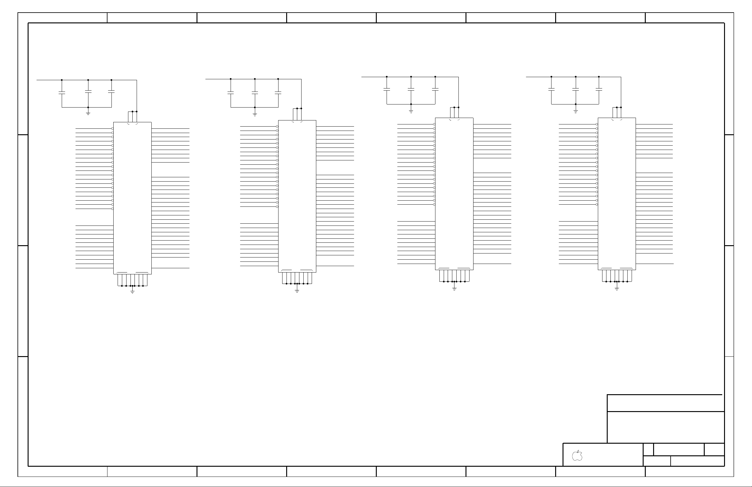
GND
DA10
SEL
DH19
DH18
DH17
DH16
DH15
DH14
DH13
DH12
DH11
DH10
DH9
DH8
DH7
DH6
DH5
DH4
DH3
DH2
DH1
DH0
DA19
DA18
DA17
DA16
DA15
DA14
DA13
DA12
DA11DB0*
DA9
DA8
DA7
DA6
DA5
DA4
DA3
DA2
DA1
DA0
DB19*
DB18*
DB17*
DB16*
DB15*
DB14*
DB13*
DB12*
DB11*
DB10*
DB9*
DB8*
DB7*
DB6*
DB5*
DB4*
DB3*
DB2*
DB1*
VDD
GND
DA10
SEL
DH19
DH18
DH17
DH16
DH15
DH14
DH13
DH12
DH11
DH10
DH9
DH8
DH7
DH6
DH5
DH4
DH3
DH2
DH1
DH0
DA19
DA18
DA17
DA16
DA15
DA14
DA13
DA12
DA11DB0*
DA9
DA8
DA7
DA6
DA5
DA4
DA3
DA2
DA1
DA0
DB19*
DB18*
DB17*
DB16*
DB15*
DB14*
DB13*
DB12*
DB11*
DB10*
DB9*
DB8*
DB7*
DB6*
DB5*
DB4*
DB3*
DB2*
DB1*
VDD
D
SIZE
OF
SHT
DRAWING NUMBER
NOTICE OF PROPRIETARY PROPERTY
I TO MAINTAIN THE DOCUMENT IN CONFIDENCE
III NOT TO REVEAL OR PUBLISH IN WHOLE OR PART
II NOT TO REPRODUCE OR COPY IT
AGREES TO THE FOLLOWING
PROPERTY OF APPLE COMPUTER, INC. THE POSSESSOR
THE INFORMATION CONTAINED HEREIN IS THE PROPRIETARY
1
2
3
4
5
67
8
12
3
4
5
6
78
B
C
D
A
B
C
D
A
REV.
APPLE COMPUTER INC.
SCALE
NONE
16BIT 2:1 DDR MUXES
BIT 48..63BIT 32..47
BIT 16..31
BIT 0..15
SEL = LOW; HOST = B PORT; A PORT = 100OHM TO GND
SEL = HIGH; HOST = A PORT; B PORT = 100OHM TO GND
2
1
C727
20%
10V
CERM
402
0.1uF
2
1
C745
402
CERM
10V
20%
0.1uF
2
1
C742
20%
10V
CERM
402
0.1uF
2
1
C732
20%
10V
CERM
402
0.1uF
2
1
C733
402
CERM
10V
20%
0.1uF
2
1
C741
20%
10V
CERM
402
0.1uF
2
1
C764
402
CERM
10V
20%
0.1uF
2
1
C734
20%
10V
CERM
402
0.1uF
2
1
C726
402
CERM
10V
20%
0.1uF
2
1
C730
20%
10V
CERM
402
0.1uF
2
1
C758
20%
10V
CERM
402
0.1uF
2
1
C757
20%
10V
CERM
402
0.1uF
F8F3E8
E3
H6H5G9G2D9D2C6
C5
E2
C2
B2
B3
B5
B6
B8
B9
C9
E9
F9
H9
J9
J8
J6
J5
J3
J2
H2
F2
E1
C1
A1
A3
A4
A6
B7
A9
B10
D10
F10
H10
K10
K8
K7
K5
J4
K2
J1
G1
D1
B1
A2
B4
A5
A7
A8
A10
C10
E10
G10
J10
K9
J7
K6
K4
K3
K1
H1
F1
U28
CRITICAL
BGA
CBTV4020
F8F3E8
E3
H6H5G9G2D9D2C6
C5
E2
C2
B2
B3
B5
B6
B8
B9
C9
E9
F9
H9
J9
J8
J6
J5
J3
J2
H2
F2
E1
C1
A1
A3
A4
A6
B7
A9
B10
D10
F10
H10
K10
K8
K7
K5
J4
K2
J1
G1
D1
B1
A2
B4
A5
A7
A8
A10
C10
E10
G10
J10
K9
J7
K6
K4
K3
K1
H1
F1
U27
CRITICAL
BGA
CBTV4020
F8F3E8
E3
H6H5G9G2D9D2C6
C5
E2
C2
B2
B3
B5
B6
B8
B9
C9
E9
F9
H9
J9
J8
J6
J5
J3
J2
H2
F2
E1
C1
A1
A3
A4
A6
B7
A9
B10
D10
F10
H10
K10
K8
K7
K5
J4
K2
J1
G1
D1
B1
A2
B4
A5
A7
A8
A10
C10
E10
G10
J10
K9
J7
K6
K4
K3
K1
H1
F1
U18
CBTV4020
BGA
CRITICAL
F8F3E8
E3
H6H5G9G2D9D2C6
C5
E2
C2
B2
B3
B5
B6
B8
B9
C9
E9
F9
H9
J9
J8
J6
J5
J3
J2
H2
F2
E1
C1
A1
A3
A4
A6
B7
A9
B10
D10
F10
H10
K10
K8
K7
K5
J4
K2
J1
G1
D1
B1
A2
B4
A5
A7
A8
A10
C10
E10
G10
J10
K9
J7
K6
K4
K3
K1
H1
F1
U16
CBTV4020
BGA
CRITICAL
C
4010
051-6338
RAM_DATA_B<13>
MEM_DQS<3>
MEM_DATA<31>
RAM_DATA_B<25>
RAM_DATA_B<45>
RAM_DATA_B<47>
MEM_DATA<5>
MEM_DATA<7>
+2_5V_INTREPID +2_5V_INTREPID
+2_5V_INTREPID
+2_5V_INTREPID
RAM_DATA_A<57>
MEM_DQM<7>
RAM_DATA_A<56>
RAM_DATA_A<48>
RAM_DATA_A<50>
RAM_DATA_A<51>
RAM_DATA_A<49>
RAM_DATA_A<53>
RAM_DATA_A<52>
RAM_DATA_A<54>
RAM_DATA_A<55>
RAM_DQS_A<6>
RAM_DQM_A<6>
MEM_MUXSEL_MSB
MEM_DATA<63>
MEM_DQS<7>
MEM_DATA<62>
MEM_DATA<60>
MEM_DATA<61>
MEM_DATA<57>
MEM_DATA<58>
MEM_DATA<59>
MEM_DATA<56>
MEM_DQM<6>
MEM_DATA<55>
MEM_DATA<54>
MEM_DQS<6>
MEM_DATA<52>
MEM_DATA<53>
MEM_DATA<50>
MEM_DATA<49>
MEM_DATA<51>
RAM_DQM_A<7>
MEM_DATA<48>
RAM_DQS_A<7>
RAM_DATA_A<62>
RAM_DATA_A<63>
RAM_DATA_A<60>
RAM_DATA_A<61>
RAM_DATA_A<59>
RAM_DATA_A<58>
RAM_DATA_B<59>
RAM_DATA_B<60>
RAM_DATA_B<61>
RAM_DATA_B<62>
RAM_DATA_B<63>
RAM_DQS_B<7>
RAM_DQM_B<7>
RAM_DATA_B<53>
RAM_DATA_B<54>
RAM_DATA_B<55>
RAM_DATA_B<51>
RAM_DATA_B<52>
RAM_DQS_B<6>
RAM_DQM_B<6>
RAM_DATA_B<56>
RAM_DATA_B<57>
RAM_DATA_B<58>
RAM_DATA_B<50>
RAM_DATA_B<49>
RAM_DATA_B<48>RAM_DATA_A<41>
MEM_DQM<5>
RAM_DATA_A<40>
RAM_DATA_A<32>
RAM_DATA_A<34>
RAM_DATA_A<35>
RAM_DATA_A<33>
RAM_DATA_A<37>
RAM_DATA_A<36>
RAM_DATA_A<38>
RAM_DATA_A<39>
RAM_DQS_A<4>
RAM_DQM_A<4>
MEM_MUXSEL_MSB
MEM_DATA<47>
MEM_DQS<5>
MEM_DATA<46>
MEM_DATA<44>
MEM_DATA<45>
MEM_DATA<41>
MEM_DATA<42>
MEM_DATA<43>
MEM_DATA<40>
MEM_DQM<4>
MEM_DATA<39>
MEM_DATA<38>
MEM_DQS<4>
MEM_DATA<36>
MEM_DATA<37>
MEM_DATA<34>
MEM_DATA<33>
MEM_DATA<35>
RAM_DQM_A<5>
MEM_DATA<32>
RAM_DQS_A<5>
RAM_DATA_A<46>
RAM_DATA_A<47>
RAM_DATA_A<44>
RAM_DATA_A<45>
RAM_DATA_A<43>
RAM_DATA_A<42>
RAM_DATA_B<43>
RAM_DATA_B<44>
RAM_DATA_B<46>
RAM_DQS_B<5>
RAM_DQM_B<5>
RAM_DATA_B<37>
RAM_DATA_B<38>
RAM_DATA_B<39>
RAM_DATA_B<35>
RAM_DATA_B<36>
RAM_DQS_B<4>
RAM_DQM_B<4>
RAM_DATA_B<40>
RAM_DATA_B<41>
RAM_DATA_B<42>
RAM_DATA_B<34>
RAM_DATA_B<33>
RAM_DATA_B<32>
RAM_DATA_A<25>
MEM_DQM<3>
RAM_DATA_A<24>
RAM_DATA_A<16>
RAM_DATA_A<18>
RAM_DATA_A<19>
RAM_DATA_A<17>
RAM_DATA_A<21>
RAM_DATA_A<20>
RAM_DATA_A<22>
RAM_DATA_A<23>
RAM_DQS_A<2>
RAM_DQM_A<2>
MEM_MUXSEL_LSB
MEM_DATA<30>
MEM_DATA<28>
MEM_DATA<29>
MEM_DATA<25>
MEM_DATA<26>
MEM_DATA<27>
MEM_DATA<24>
MEM_DQM<2>
MEM_DATA<23>
MEM_DATA<22>
MEM_DQS<2>
MEM_DATA<20>
MEM_DATA<21>
MEM_DATA<18>
MEM_DATA<17>
MEM_DATA<19>
RAM_DQM_A<3>
MEM_DATA<16>
RAM_DQS_A<3>
RAM_DATA_A<30>
RAM_DATA_A<31>
RAM_DATA_A<28>
RAM_DATA_A<29>
RAM_DATA_A<27>
RAM_DATA_A<26>
RAM_DATA_B<27>
RAM_DATA_B<28>
RAM_DATA_B<29>
RAM_DATA_B<30>
RAM_DATA_B<31>
RAM_DQS_B<3>
RAM_DQM_B<3>
RAM_DATA_B<21>
RAM_DATA_B<22>
RAM_DATA_B<23>
RAM_DATA_B<19>
RAM_DATA_B<20>
RAM_DQS_B<2>
RAM_DQM_B<2>
RAM_DATA_B<24>
RAM_DATA_B<26>
RAM_DATA_B<18>
RAM_DATA_B<17>
RAM_DATA_B<16>
RAM_DATA_A<9>
MEM_DQM<1>
RAM_DATA_A<8>
RAM_DATA_A<0>
RAM_DATA_A<2>
RAM_DATA_A<3>
RAM_DATA_A<1>
RAM_DATA_A<5>
RAM_DATA_A<4>
RAM_DATA_A<6>
RAM_DATA_A<7>
RAM_DQS_A<0>
RAM_DQM_A<0>
MEM_MUXSEL_LSB
MEM_DATA<15>
MEM_DQS<1>
MEM_DATA<14>
MEM_DATA<12>
MEM_DATA<13>
MEM_DATA<9>
MEM_DATA<10>
MEM_DATA<11>
MEM_DATA<8>
MEM_DQM<0>
MEM_DATA<6>
MEM_DQS<0>
MEM_DATA<4>
MEM_DATA<2>
MEM_DATA<1>
MEM_DATA<3>
RAM_DQM_A<1>
MEM_DATA<0>
RAM_DQS_A<1>
RAM_DATA_A<14>
RAM_DATA_A<15>
RAM_DATA_A<12>
RAM_DATA_A<13>
RAM_DATA_A<11>
RAM_DATA_A<10>
RAM_DATA_B<11>
RAM_DATA_B<12>
RAM_DATA_B<14>
RAM_DATA_B<15>
RAM_DQS_B<1>
RAM_DQM_B<1>
RAM_DATA_B<5>
RAM_DATA_B<6>
RAM_DATA_B<7>
RAM_DATA_B<3>
RAM_DATA_B<4>
RAM_DQS_B<0>
RAM_DQM_B<0>
RAM_DATA_B<8>
RAM_DATA_B<9>
RAM_DATA_B<10>
RAM_DATA_B<2>
RAM_DATA_B<1>
RAM_DATA_B<0>
38 38
38
38
16 16
16
16
15 15
15
15
35 35
35
35
35
35
35
35
35
35
35
35
10 10
10
10
35
35
35
35
35
35
35
35
35
35
35
35
35
10
35
35
35
35
35
35
35
35
35
35
35
35
35
35
35
35
35
35
35
35
35
35
35
35
35
35
35
35
35
35
35
35
35
35
35
35
35
35
35
35
35
35
35
35
35
35
35 35
35
35
35
35
35
35
35
35
35
35
35
35
10
35
35
35
35
35
35
35
35
35
35
35
35
35
35
35
35
35
35
35
35
35
35
35
35
35
35
35
35
35
35
35
35
35
35
35
35
35
35
35
35
35
35
35
35
35
35
35
35
35
35
35
35
35
35
35
35
35
35
10
35
35
35
35
35
35
35
35
35
35
35
35
35
35
35
35
35
35
35
35
35
35
35
35
35
35
35
35
35
35
35
35
35
35
35
35
35
35
35
35
35
35
35
35
35
35
35
35
35
35
35
35
35
35
35
35
35
10
35
35
35
35
35
35
35
35
35
35
35
35
35
35
35
35
35
35
35
35
35
35
35
35
35
35
35
35
35
35
35
35
35
35
35
35
35
35
35
35
35
35
35
35
11
9
9
11
11
11
9
9
9 9
9
9
11
9
11
11
11
11
11
11
11
11
11
11
11
9
9
9
9
9
9
9
9
9
9
9
9
9
9
9
9
9
9
9
11
9
11
11
11
11
11
11
11
11
11
11
11
11
11
11
11
11
11
11
11
11
11
11
11
11
11
11
11 11
9
11
11
11
11
11
11
11
11
11
11
11
9
9
9
9
9
9
9
9
9
9
9
9
9
9
9
9
9
9
9
11
9
11
11
11
11
11
11
11
11
11
11
11
11
11
11
11
11
11
11
11
11
11
11
11
11
11
11
9
11
11
11
11
11
11
11
11
11
11
11
9
9
9
9
9
9
9
9
9
9
9
9
9
9
9
9
9
11
9
11
11
11
11
11
11
11
11
11
11
11
11
11
11
11
11
11
11
11
11
11
11
11
11
11
11
11
9
11
11
11
11
11
11
11
11
11
11
11
9
9
9
9
9
9
9
9
9
9
9
9
9
9
9
9
9
11
9
11
11
11
11
11
11
11
11
11
11
11
11
11
11
11
11
11
11
11
11
11
11
11
11
11
11
Page 11
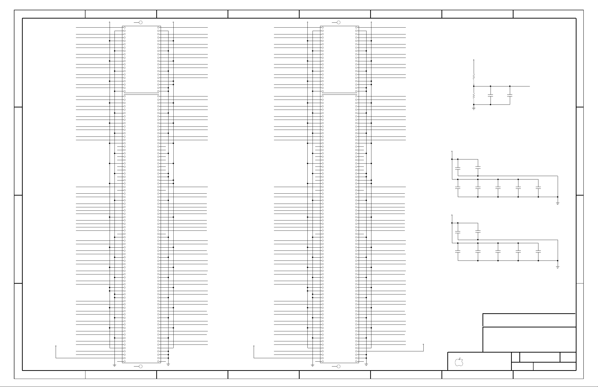
DQ58
RFU18
KEY
VDD6
VSS6
VSS8
VDD5
DQ15
DQ13
DQ14
VSS5
DM1
VDD3
VSS3
DQ7
DQ12
DQ6
DM0
DQ4
DQ5
VSS1
VREF1
VDD1
SA1
SA2
RFU19
SA0
VDD32
DQ63
DQ62
VSS32
DQ61
VDD30
DQ60
DQ55
DM7
VSS30
DQ54
DM6
VDD28
DQ53
DQ52
VDD25
CK1*
CK1
VSS28
DQ47
DQ46
VDD23
VSS25
DM5
DQ45
DQ44
DM4
DQ39
VSS23
DQ38
DQ37
RFU17
DQ36
VSS21
VDD21
VDD19
RAS*
BA1
CAS*
S1*
A6
A4
A2
A0
VSS19
A8
A11
VDD17
RFU15
CKE0
VDD15
VSS17
RFU11
VSS16
RFU9
VDD14
RFU3
VSS14
RFU5
RFU7
RFU1
VDD12
VSS12
DM3
DQ31
DQ30
DQ29
VSS10
VDD10
DQ28
DQ23
DM2
DQ20
VDD8
DQ21
DQ22
VDDSPD
SCL
SDA
VDD31
VSS31
DQ59
DQS7
DQ51
VDD29
DQ56
VSS29
DQ57
DQ48
DQS6
VDD27
DQ49
DQ50
DQ43
VSS26
VDD26
VDD24
VSS27
DQ41
DQS5
VSS24
VDD22
DQ42
DQ34
VSS22
DQ35
DQS4
DQ40
VDD20
RFU16
DQ32
VSS20
DQ33
S0*
VDD18
BA0
A10_AP
WE*
A1
A5
A3
A9
A7
VSS18
CKE1
RFU14
RFU13
VDD16
VDD13
VSS15
RFU10
RFU8
RFU12
RFU0
RFU4
VSS13
RFU2
RFU6
VSS11
DQ26
DQ27
DQS3
VDD11
DQ19
DQ24
VDD9
VSS9
DQ25
DQ18
DQ16
VDD7
DQ17
DQS2
DQ11
VDD4
VSS7
CK0*
CK0
DQS1
VSS4
DQ10
VDD2
DQ9
DQ2
DQS0
DQ8
DQ3
VSS2
VDD0
DQ0
DQ1
VSS0
VREF0
A12
(1 OF 2)(2 OF 2)
DQ58
RFU18
KEY
VDD6
VSS6
VSS8
VDD5
DQ15
DQ13
DQ14
VSS5
DM1
VDD3
VSS3
DQ7
DQ12
DQ6
DM0
DQ4
DQ5
VSS1
VREF1
VDD1
SA1
SA2
RFU19
SA0
VDD32
DQ63
DQ62
VSS32
DQ61
VDD30
DQ60
DQ55
DM7
VSS30
DQ54
DM6
VDD28
DQ53
DQ52
VDD25
CK1*
CK1
VSS28
DQ47
DQ46
VDD23
VSS25
DM5
DQ45
DQ44
DM4
DQ39
VSS23
DQ38
DQ37
RFU17
DQ36
VSS21
VDD21
VDD19
RAS*
BA1
CAS*
S1*
A6
A4
A2
A0
VSS19
A8
A11
VDD17
RFU15
CKE0
VDD15
VSS17
RFU11
VSS16
RFU9
VDD14
RFU3
VSS14
RFU5
RFU7
RFU1
VDD12
VSS12
DM3
DQ31
DQ30
DQ29
VSS10
VDD10
DQ28
DQ23
DM2
DQ20
VDD8
DQ21
DQ22
VDDSPD
SCL
SDA
VDD31
VSS31
DQ59
DQS7
DQ51
VDD29
DQ56
VSS29
DQ57
DQ48
DQS6
VDD27
DQ49
DQ50
DQ43
VSS26
VDD26
VDD24
VSS27
DQ41
DQS5
VSS24
VDD22
DQ42
DQ34
VSS22
DQ35
DQS4
DQ40
VDD20
RFU16
DQ32
VSS20
DQ33
S0*
VDD18
BA0
A10_AP
WE*
A1
A5
A3
A9
A7
VSS18
CKE1
RFU14
RFU13
VDD16
VDD13
VSS15
RFU10
RFU8
RFU12
RFU0
RFU4
VSS13
RFU2
RFU6
VSS11
DQ26
DQ27
DQS3
VDD11
DQ19
DQ24
VDD9
VSS9
DQ25
DQ18
DQ16
VDD7
DQ17
DQS2
DQ11
VDD4
VSS7
CK0*
CK0
DQS1
VSS4
DQ10
VDD2
DQ9
DQ2
DQS0
DQ8
DQ3
VSS2
VDD0
DQ0
DQ1
VSS0
VREF0
A12
D
SIZE
OF
SHT
DRAWING NUMBER
NOTICE OF PROPRIETARY PROPERTY
I TO MAINTAIN THE DOCUMENT IN CONFIDENCE
III NOT TO REVEAL OR PUBLISH IN WHOLE OR PART
II NOT TO REPRODUCE OR COPY IT
AGREES TO THE FOLLOWING
PROPERTY OF APPLE COMPUTER, INC. THE POSSESSOR
THE INFORMATION CONTAINED HEREIN IS THE PROPRIETARY
1
2
3
4
5
67
8
12
3
4
5
6
78
B
C
D
A
B
C
D
A
REV.
APPLE COMPUTER INC.
SCALE
NONE
NCNC
NC
NC
NCNC
on the PCB for additional mounting
NOTE: The SODIMM connector footprint has a through-hole slot
NC
NC
NC
NC
NC
NC
NC
NC
ADDR=0XA0(WR)/0XA1(RD)
NC
NC
NC
NC
NC
NC
NC
NC
NC
NC
NC
SLOT "A"
LOWER SLOT
FACTORY SLOT
NC
ADDR=0XA2(WR)/0XA3(RD)
SLOT "B"
UPPER SLOT
CUSTOMER SLOT
NC
NC
NC
NC
NC
NC
NC
NC
NC
NC
NC
NC
NC
NC
NC
NC
NC
NC
DDR SODIMM CONNS
SLOT "B"
SLOT "A"
DDR BYPASS
DDR VREF
ONE 0.1UF PER SLOT
2
1
C140
0.1uF
20%
10V
402
CERM
2
1
C156
0.1uF
20%
10V
402
CERM
2
1
C132
0.1uF
10V
402
CERM
20%
119B
51B
40B39B
38B
28B27B
16B
186B185B
174B
15B
173B
162B161B
159B
150B149B
138B137B
126B125B
4B
104B103B
90B
88B87B
76B75B
64B63B
52B
3B
2B1B
197B
57B
46B45B
36B
34B33B
22B
192B191B
180B
21B
179B
168B167B
157B
156B155B
144B143B
132B131B
10B
114B113B
94B93B
92B
82B81B
70B69B
58B
9B
193B
195B
198B
196B
194B
122B121B
84B83B
80B79B
78B77B
74B73B
72B
200B199B
124B123B
98B97B
91B
89B
86B85B
71B
118B
402
401
183B
169B
147B
133B
61B
47B
25B
11B
23B
19B
18B
14B
190B
188B
182B
178B
8B
189B
187B
181B
177B
176B
172B
166B
164B
175B
171B
6B
165B
163B
154B
152B
146B
142B
153B
151B
145B
141B
17B
140B
136B
130B
128B
139B
135B
129B
127B
68B
66B
13B
60B
56B
67B
65B
59B
55B
54B
50B
44B
42B
7B
53B
49B
43B
41B
32B
30B
24B
20B
31B
29B
5B
184B
170B
148B
134B
62B
48B
26B
12B
95B 96B
158B
160B
37B
35B
120B
116B
117B
101B 102B
105B 106B
107B 108B
109B 110B
111B
99B
100B
115B
112B
J25
CRITICAL
F-RT-SM
DDR-SO-DIMM-DUAL
119A
51A
40A39A
38A
28A27A
16A
186A185A
174A
15A
173A
162A161A
159A
150A149A
138A137A
126A125A
4A
104A103A
90A
88A87A
76A75A
64A63A
52A
3A
2A1A
197A
57A
46A45A
36A
34A33A
22A
192A191A
180A
21A
179A
168A167A
157A
156A155A
144A143A
132A131A
10A
114A113A
94A93A
92A
82A81A
70A69A
58A
9A
193A
195A
198A
196A
194A
122A121A
84A83A
80A79A
78A77A
74A73A
72A
200A199A
124A123A
98A97A
91A
89A
86A85A
71A
118A
404
403
183A
169A
147A
133A
61A
47A
25A
11A
23A
19A
18A
14A
190A
188A
182A
178A
8A
189A
187A
181A
177A
176A
172A
166A
164A
175A
171A
6A
165A
163A
154A
152A
146A
142A
153A
151A
145A
141A
17A
140A
136A
130A
128A
139A
135A
129A
127A
68A
66A
13A
60A
56A
67A
65A
59A
55A
54A
50A
44A
42A
7A
53A
49A
43A
41A
32A
30A
24A
20A
31A
29A
5A
184A
170A
148A
134A
62A
48A
26A
12A
95A 96A
158A
160A
37A
35A
120A
116A
117A
101A 102A
105A 106A
107A 108A
109A 110A
111A
99A
100A
115A
112A
J25
CRITICAL
F-RT-SM
DDR-SO-DIMM-DUAL
2
1
C404
10uF
20%
6.3V
CERM
805
2
1
C128
10uF
20%
6.3V
CERM
805
2
1
R299
402
MF
1/16W
1%
1K
2
1
R303
1K
1%
1/16W
MF
402
2
1
C397
0.1uF
402
CERM
10V
20%
2
1
C403
0.1uF
20%
10V
CERM
402
+2_5V_MAIN+2_5V_MAIN
+2_5V_MAIN
+2_5V_MAIN
+2_5V_MAIN+2_5V_MAIN
+3V_MAIN +3V_MAIN
+3V_MAIN
2
1
C169
CERM
402
10V
20%
0.1uF
2
1
C391
0.1uF
10V
402
CERM
20%
2
1
C356
20%
CERM
402
10V
0.1uF
2
1
C211
0.1uF
20%
10V
402
CERM
2
1
C127
0.1uF
20%
10V
402
CERM
+2_5V_MAIN
2
1
C174
10uF
805
CERM
6.3V
20%
2
1
C150
20%
CERM
402
10V
0.1uF
2
1
C157
10uF
805
CERM
6.3V
20%
2
1
C383
0.1uF
20%
10V
402
CERM
051-6338
11 40
C
RAM_DATA_B<37>
RAM_DATA_B<63>
RAM_DATA_B<62>
RAM_DQM_B<7>
RAM_DATA_B<61>
RAM_DATA_B<60>
RAM_DATA_B<55>
RAM_DATA_B<54>
RAM_DQM_B<6>
RAM_DATA_B<53>
RAM_DATA_B<52>
SYSCLK_DDRCLK_B1
SYSCLK_DDRCLK_B1_L
RAM_DATA_B<47>
RAM_DATA_B<46>
RAM_DQM_B<5>
RAM_DATA_B<45>
RAM_DATA_B<44>
RAM_DATA_B<39>
RAM_DATA_B<38>
RAM_DQM_B<4>
RAM_DATA_B<36>
RAM_CS_L<3>
RAM_CAS_L
RAM_RAS_L
RAM_BA<1>
RAM_ADDR<0>
RAM_ADDR<2>
RAM_ADDR<4>
RAM_ADDR<6>
RAM_ADDR<8>
RAM_ADDR<11>
RAM_CKE<2>
RAM_DATA_B<31>
RAM_DATA_B<30>
RAM_DQM_B<3>
RAM_DATA_B<29>
RAM_DATA_B<28>
RAM_DATA_B<22>
RAM_DQM_B<2>
RAM_DATA_B<21>
RAM_DATA_B<20>
RAM_DATA_B<15>
RAM_DATA_B<14>
RAM_DQM_B<1>
RAM_DATA_B<13>
RAM_DATA_B<12>
RAM_DATA_B<7>
RAM_DATA_B<6>
RAM_DQM_B<0>
RAM_DATA_B<5>
RAM_DATA_B<4>
DDR_VREF
INT_I2C_CLK0
INT_I2C_DATA0
RAM_DATA_B<59>
RAM_DATA_B<58>
RAM_DQS_B<7>
RAM_DATA_B<57>
RAM_DATA_B<56>
RAM_DATA_B<51>
RAM_DATA_B<50>
RAM_DQS_B<6>
RAM_DATA_B<49>
RAM_DATA_B<48>
RAM_DATA_B<43>
RAM_DATA_B<42>
RAM_DQS_B<5>
RAM_DATA_B<41>
RAM_DATA_B<40>
RAM_DATA_B<35>
RAM_DATA_B<34>
RAM_DQS_B<4>
RAM_DATA_B<33>
RAM_DATA_B<32>
RAM_CS_L<2>
RAM_WE_L
RAM_BA<0>
RAM_ADDR<10>
RAM_ADDR<1>
RAM_ADDR<3>
RAM_ADDR<5>
RAM_ADDR<7>
RAM_ADDR<9>
RAM_ADDR<12>
RAM_CKE<3>
RAM_DATA_B<27>
RAM_DATA_B<26>
RAM_DQS_B<3>
RAM_DATA_B<25>
RAM_DATA_B<24>
RAM_DATA_B<19>
RAM_DATA_B<18>
RAM_DQS_B<2>
RAM_DATA_B<17>
RAM_DATA_B<16>
SYSCLK_DDRCLK_B0_L
SYSCLK_DDRCLK_B0
RAM_DATA_B<11>
RAM_DATA_B<10>
RAM_DQS_B<1>
RAM_DATA_B<9>
RAM_DATA_B<8>
RAM_DATA_B<3>
RAM_DATA_B<2>
RAM_DQS_B<0>
RAM_DATA_B<1>
RAM_DATA_B<0>
DDR_VREF
DDR_VREF
RAM_DATA_B<23>
RAM_DATA_A<38>
RAM_DQM_A<4>
RAM_BA<1>
RAM_DATA_A<28>
RAM_DATA_A<15>
RAM_DATA_A<63>
RAM_DATA_A<62>
RAM_DQM_A<7>
RAM_DATA_A<61>
RAM_DATA_A<60>
RAM_DATA_A<55>
RAM_DATA_A<54>
RAM_DQM_A<6>
RAM_DATA_A<53>
RAM_DATA_A<52>
SYSCLK_DDRCLK_A1
SYSCLK_DDRCLK_A1_L
RAM_DATA_A<47>
RAM_DATA_A<46>
RAM_DQM_A<5>
RAM_DATA_A<45>
RAM_DATA_A<44>
RAM_DATA_A<39>
RAM_DATA_A<37>
RAM_DATA_A<36>
RAM_CS_L<1>
RAM_CAS_L
RAM_ADDR<0>
RAM_ADDR<2>
RAM_ADDR<4>
RAM_ADDR<6>
RAM_ADDR<8>
RAM_ADDR<11>
RAM_CKE<0>
RAM_DATA_A<31>
RAM_DATA_A<30>
RAM_DQM_A<3>
RAM_DATA_A<29>
RAM_DATA_A<23>
RAM_DQM_A<2>
RAM_DATA_A<21>
RAM_DATA_A<20>
RAM_DATA_A<14>
RAM_DQM_A<1>
RAM_DATA_A<13>
RAM_DATA_A<12>
RAM_DATA_A<7>
RAM_DATA_A<6>
RAM_DQM_A<0>
RAM_DATA_A<5>
RAM_DATA_A<4>
DDR_VREF
RAM_DATA_A<56>
RAM_DATA_A<50>
INT_I2C_CLK0
INT_I2C_DATA0
RAM_DATA_A<59>
RAM_DATA_A<58>
RAM_DQS_A<7>
RAM_DATA_A<57>
RAM_DATA_A<51>
RAM_DQS_A<6>
RAM_DATA_A<49>
RAM_DATA_A<48>
RAM_DATA_A<43>
RAM_DATA_A<42>
RAM_DQS_A<5>
RAM_DATA_A<41>
RAM_DATA_A<40>
RAM_DATA_A<35>
RAM_DATA_A<34>
RAM_DQS_A<4>
RAM_DATA_A<33>
RAM_DATA_A<32>
RAM_CS_L<0>
RAM_WE_L
RAM_BA<0>
RAM_ADDR<10>
RAM_ADDR<1>
RAM_ADDR<3>
RAM_ADDR<5>
RAM_ADDR<7>
RAM_ADDR<9>
RAM_ADDR<12>
RAM_CKE<1>
RAM_DATA_A<27>
RAM_DATA_A<26>
RAM_DQS_A<3>
RAM_DATA_A<25>
RAM_DATA_A<24>
RAM_DATA_A<19>
RAM_DATA_A<18>
RAM_DQS_A<2>
RAM_DATA_A<17>
RAM_DATA_A<16>
SYSCLK_DDRCLK_A0_L
SYSCLK_DDRCLK_A0
RAM_DATA_A<11>
RAM_DATA_A<10>
RAM_DQS_A<1>
RAM_DATA_A<9>
RAM_DATA_A<8>
RAM_DATA_A<3>
RAM_DATA_A<2>
RAM_DQS_A<0>
RAM_DATA_A<1>
RAM_DATA_A<0>
RAM_RAS_L
RAM_DATA_A<22>
DDR_VREF
39
39
39
39
23
23
23
23
35
35
35
35
35
35
35
35
35
13
13
35
35
35
35
35
35
35
35
35
35
35
35
35
35
35
35
35
13
13
35
35
35
35
35
35
35
35
35
35
35
35
35
35
35
35
35
35
35
35
35
35
35
35
35
35
35
35
35
35
35
35
35
11
11
11
11
11
11
11
11
11
35
35
35
35
35
35
35
35
35
35
35
35
35
35
35
35
35
35
35
35
38
11
11
35
35
35
35
35
35
35
35
35
35
35
35
35
35
35
35
35
35
35
35
35
11
11
11
11
11
11
11
11
11
35
35
35
35
35
35
35
35
35
35
35
35
35
35
35
35
35
35
35
35
35
35
35
38
38
35
35
35
11
35
35
35
35
35
35
35
35
35
35
35
35
35
35
35
35
35
35
35
35
35
35
35
11
11
11
11
11
11
11
35
35
35
35
35
35
35
35
35
35
35
35
35
35
35
35
35
35
38
35
35
11
11
35
35
35
35
35
35
35
35
35
35
35
35
35
35
35
35
35
35
35
11
11
11
11
11
11
11
11
11
35
35
35
35
35
35
35
35
35
35
35
35
35
35
35
35
35
35
35
35
35
35
35
11
35
38
10
10
10
10
10
10
10
10
10
10
10
9
9
10
10
10
10
10
10
10
10
10
9
9
9
9
9
9
9
9
9
9
9
10
10
10
10
10
10
10
10
10
10
10
10
10
10
10
10
10
10
10
11
6
6
10
10
10
10
10
10
10
10
10
10
10
10
10
10
10
10
10
10
10
10
9
9
9
9
9
9
9
9
9
9
9
10
10
10
10
10
10
10
10
10
10
9
9
10
10
10
10
10
10
10
10
10
10
11
11
10
10
10
9
10
10
10
10
10
10
10
10
10
10
10
10
9
9
10
10
10
10
10
10
10
10
9
9
9
9
9
9
9
9
9
10
10
10
10
10
10
10
10
10
10
10
10
10
10
10
10
10
11
10
10
6
6
10
10
10
10
10
10
10
10
10
10
10
10
10
10
10
10
10
10
9
9
9
9
9
9
9
9
9
9
9
10
10
10
10
10
10
10
10
10
10
9
9
10
10
10
10
10
10
10
10
10
10
9
10
11
Page 12
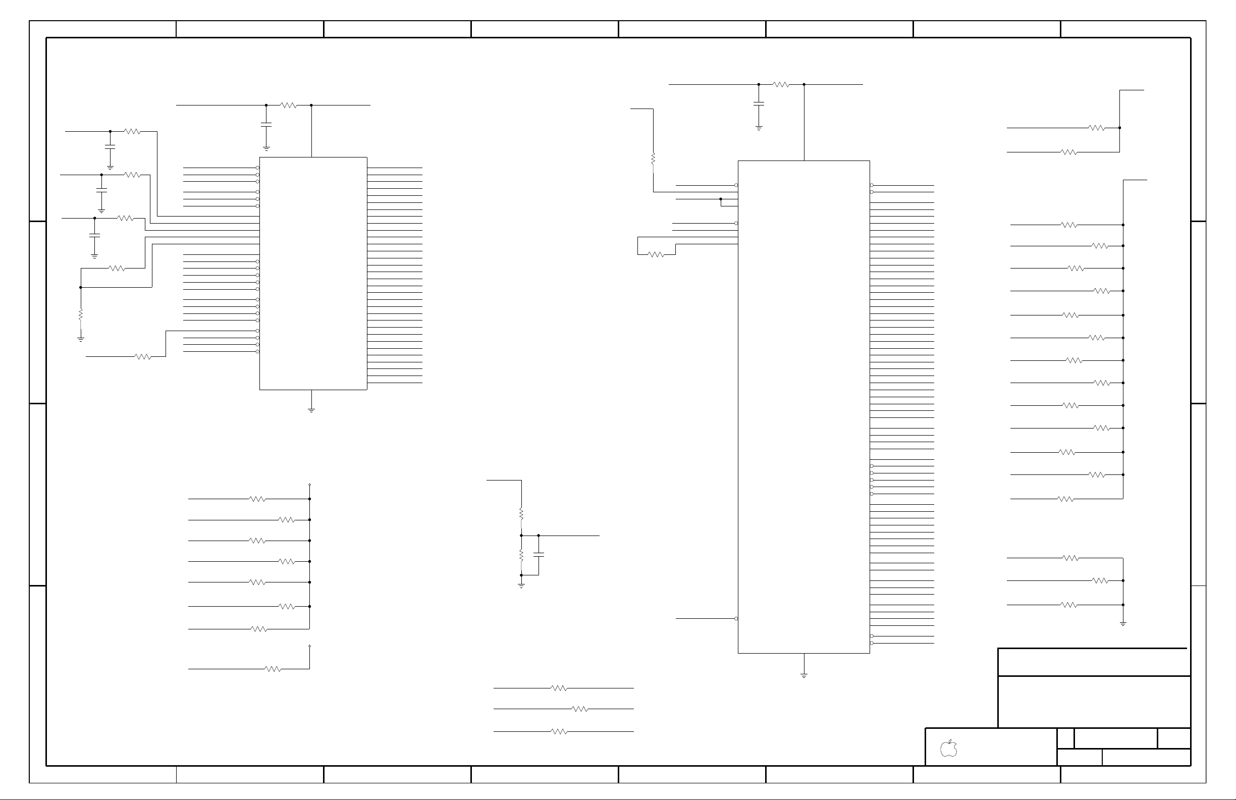
(PLL4)
VDD15A_6
(PLL4)
VSSA_6
ROM_WE
ROM_OE
PCI_STOP
PCI_DEVSEL
PCI_CBE_3
PCI_CBE_2
PCI_CBE_1
PCI_CBE_0
ROM_CS
PCI_CLK_IN
PCI_CLK_OUT
PCI_CLK2
PCI_CLK1
PCI_CLK0
PCI_FRAME
PCI_PAR
PCI_TRDY
PCI_IRDY
PCI_REQ_2
PCI_REQ_1
PCI_REQ_0
PCI_GNT_0
PCI_GNT_1
PCI_GNT_2
PCI/ROM
INTERFACE
PCIAD_31
PCIAD_30
PCIAD_28
PCIAD_27
PCIAD_26
PCIAD_25
PCIAD_29
PCIAD_19
PCIAD_18
PCIAD_17
PCIAD_16
PCIAD_15
PCIAD_23
PCIAD_24
PCIAD_20
PCIAD_21
PCIAD_22
PCIAD_14
(7 OF 9)
PCIAD_11
PCIAD_10
PCIAD_12
PCIAD_13
PCIAD_9
PCIAD_6
PCIAD_5
PCIAD_7
PCIAD_8
PCIAD_4
PCIAD_3
PCIAD_1
PCIAD_2
PCIAD_0
ROM_OVRLY_EN
VSSA_5
(PLL5)
(PLL5)
VDD15A_5
STP_AGP
AGPPVT
AGPVREF0
AGPVREF1
AGP_BUSY
AGP_CLK
AGP_FB_IN
AGP_FB_OUT
AGPAD0
AGPREQ
AGPGNT
AGP_SBA3
AGP_SBA2
AGP_SBA1
AGP_SBA0
AGPCBE_3
AGPFRAME
AGPTRDY
AGPIRDY
AGPSTOP
AGPDEVSEL
AGPPAR
AGPAD31
AGPAD30
AGPCBE_0
AGPCBE_1
AGPCBE_2
AGP_ST2
AGP_AD_STB0_P
AGP_AD_STB0_N
AGP_AD_STB1_P
AGP_AD_STB1_N
AGPPIPE
AGPRBF
AGP_ST1
AGP_SBA7
AGP_SB_STB_P
AGP_SB_STB_N
AGP_ST0
AGP_WBF
AGP
INTERFACES
AGP_SBA6
AGP_SBA5
AGP_SBA4
AGPAD29
AGPAD28
AGPAD27
AGPAD26
AGPAD25
AGPAD24
AGPAD23
AGPAD22
AGPAD21
AGPAD20
AGPAD19
AGPAD18
AGPAD17
AGPAD16
AGPAD15
AGPAD14
AGPAD13
AGPAD12
AGPAD11
AGPAD10
AGPAD9
AGPAD8
AGPAD7
AGPAD6
AGPAD5
AGPAD4
AGPAD3
AGPAD2
AGPAD1
(3 OF 9)
D
SIZE
OF
SHT
DRAWING NUMBER
NOTICE OF PROPRIETARY PROPERTY
I TO MAINTAIN THE DOCUMENT IN CONFIDENCE
III NOT TO REVEAL OR PUBLISH IN WHOLE OR PART
II NOT TO REPRODUCE OR COPY IT
AGREES TO THE FOLLOWING
PROPERTY OF APPLE COMPUTER, INC. THE POSSESSOR
THE INFORMATION CONTAINED HEREIN IS THE PROPRIETARY
1
2
3
4
5
67
8
12
3
4
5
6
78
B
C
D
A
B
C
D
A
REV.
APPLE COMPUTER INC.
SCALE
NONE
VIN = 1.5V
VOUT = 3.3V
PCI PULL-UPS
NOTE: Designs using AGP slot should
SIMPLY PROVIDING REFERENCE TO CHIP
BECAUSE SINGLE AGP PWR PLANE AND CLOSE PROXIMITY OF CHIPS
AGP I/O REFERENCE
(PLACE CLOSE TO INTREPID AGP BALLS)
Vin = Vcore (1.5V)
PLACE CLOSE TO INTREPID SIDE
SERIES RESISTORS FOR BOOTROM CONTROL SIGNALS
AGP PULL-UPS/PULL DOWNS
INTREPID AGP/PCI
Vout = AGPIO (1.5V)
Vout = AGPIO (1.5V)
AGP_FB_CLK IS ROUTED THE SAME LENGTH AS CLK66M_GPU_AGP
LONGEST PCI CLOCK ROUTE
INTREPID
PLACE NEAR
PCI FEEDBACK CLOCK MATCHES
use 52-ohm a resistor here.
BECAUSE THIS CHIP IS POWERED DURING SLEEP
NEC USB2 REQ REMAINS ON +3V_MAIN
402
4.7
5%
1/16W
MF
21
R197
402
5%
1/16W
MF
0
21
R246
60.4
402
MF
1/16W
1%
2
1
R245
SM1
1/16W
5%
10K
63
RP34
MF
1/16W
5%
4.7
402
21
R167
CERM
6.3V
20%
402
0.22uF
2
1
C190
INTREPID-REV2.1
BGA
CRITICAL
J10
J11
AN9
AK17
AR7
AM9
AT15
AR15
AT17
AR16
AR17
AT14
AH16
AN17
AN18
AT16
AN16
AM17
AM18
AJ19
AT18
AH18
AR18
AJ15
AM16
AK16
AR14
AR9
AK13
AH13
AN11
AT8
AN10
AM15
AN15
AJ8
AK14
AT13
AN14
AH15
AK15
AR13
AM11
AT12
AJ11
AR12
AK12
AM13
AN13
AT10
AT11
AK11
AN12
AM12
AR11
AT9
AR10
AR8
AM10
U51
33
402
MF
1/16W
5%
21
R272
33
5%
1/16W
MF
402
21
R230
402
5%
1/16W
MF
33
21
R264
47
5%
1/16W
MF
402
2
1
R244
+3V_SLEEP
SM1
10K
5%
1/16W
72
RP33
SM1
10K
5%
1/16W
54
RP33
SM1
5%
10K
1/16W
54
RP36
SM1
1/16W
5%
10K
63
RP36
SM1
10K
5%
1/16W
81
RP36
SM1
1/16W
5%
10K
72
RP36
10K
5%
1/16W
SM1
63
RP33
SM1
1/16W
5%
10K
81
RP33
402
MF
1/16W
5%
22
21
R282
402
MF
1/16W
5%
22
21
R278
402
MF
1/16W
5%
22
21
R277
402
MF
1/16W
5%
33
21
R252
1/16W
5%
MF
402
22
21
R273
NO STUFF
12PF
5%
50V
CERM
402
2
1
C311
NO STUFF
402
CERM
50V
5%
12PF
2
1
C362
NO STUFF
402
CERM
50V
5%
12PF
2
1
C372
10K
5%
1/16W
402
MF
21
R553
402
MF
1/16W
5%
10K
21
R318
10K
5%
1/16W
MF
402
21
R316
10K
5%
1/16W
MF
402
21
R314
10K
5%
1/16W
MF
402
21
R317
10K
5%
1/16W
MF
402
21
R552
10K
5%
1/16W
MF
402
21
R334
10K
5%
1/16W
MF
402
21
R308
+3V_MAIN
402
MF
1/16W
5%
10K
21
R255
402
MF
1/16W
10K
5%
21
R239
10K
5%
1/16W
MF
402
21
R254
402
MF
1/16W
5%
10K
21
R256
10K
5%
1/16W
MF
402
21
R253
402
MF
1/16W
10K
5%
21
R235
4.99K
1%
1/16W
MF
402
2
1
R225
4.99K
1%
1/16W
MF
402
2
1
R219
6.3V
402
CERM
20%
0.22uF
2
1
C291
SM1
1/16W
10K
5%
81
RP34
SM1
1/16W
5%
10K
54
RP34
SM1
1/16W
5%
10K
72
RP34
INTREPID-REV2.1
BGA
CRITICAL
V13
V14
AN19
AK30
AR30
AT30
AN29
AH25
AG25
AN30
AM30
AT31
AR31
AN31
AM31
AR32
AT32
AK25
AK27
AK28
AT19
AK21
AK22
AK20
AK19
AB21
AB20
AR29
AM28
AT33
AK24
AJ24
AJ29
AT29
AT28
AM29
AN28
AM27
AL25
AN24
AT23
AM20
AT22
AM21
AN21
AR21
AN20
AT21
AN27
AR28
AR20
AT27
AR27
AM26
AN26
AM25
AT26
AR26
AL24
AN25
AM24
AT20
AR25
AT25
AR24
AM23
AT24
AR23
AN23
AM22
AN22
AR22
AM19
AR19
U51
402
20%
6.3V
CERM
0.22uF
2
1
C270
4012
051-6338
C
PCI_IRDY_L
CBUS_PCI_REQ_L
PCI_TRDY_L
NEC_PCI_REQ_L
AGP_AD<20>
AGP_GNT_L
AGP_AD<21>
AIRPORT_PCI_REQ_L
CLK33M_NEC_UF
CLK33M_CBUS
+1_5V_INTREPID_PLL
CLK33M_NEC
CLK33M_CBUS_UF
CLK33M_AIRPORT
CLK33M_AIRPORT_UF
+1_5V_INTREPID_PLL6
STOP_AGP_L
+3V_GPU
AGP_BUSY_L
AGP_RBF_L
+1_5V_AGP
AGP_DEVSEL_L
AGP_FRAME_L
AGP_AD<13>
AGP_AD<9>
AGP_AD<6>
AGP_AD<28>
PCI_AD<19>
AGP_PIPE_L
AGP_STOP_L
AGP_AD<17>
AGP_TRDY_L
AGP_AD<7>
AGP_AD<8>
AGP_AD<5>
INT_PCI_FB_IN
CLK66M_GPU_AGP_UF
CLK66M_GPU_AGP
CLK66M_AGP_1_5V_TP
AGP_BUSY_L
INT_AGP_FB_IN
INT_AGP_FB_OUT
AGP_SB_STB_L
AGP_AD_STB_L<1>
AGP_SB_STB
AGP_AD_STB<0>
AGP_WBF_L
AGP_IRDY_L
AGP_AD_STB_L<0>
AGP_AD_STB<1>
AGP_REQ_L
INT_ROM_RW_L
ROM_RW_L
INT_ROM_CS_L
ROM_CS_L
INT_ROM_OE_L
ROM_OE_L
+1_5V_INTREPID_PLL
AGP_WBF_L
AGP_RBF_L
AGP_PIPE_L
AGP_AD_STB_L<0>
AGP_AD_STB<0>
AGP_AD_STB_L<1>
AGP_AD_STB<1>
AGP_ST<1>
AGP_ST<2>
AGP_ST<0>
AGP_SB_STB_L
AGP_SB_STB
AGP_SBA<7>
AGP_SBA<6>
AGP_SBA<5>
AGP_SBA<4>
AGP_SBA<3>
AGP_SBA<2>
AGP_SBA<0>
AGP_DEVSEL_L
AGP_STOP_L
AGP_IRDY_L
AGP_TRDY_L
AGP_FRAME_L
AGP_PAR
AGP_CBE<3>
AGP_CBE<2>
AGP_CBE<1>
AGP_CBE<0>
AGP_AD<31>
AGP_AD<30>
AGP_AD<29>
AGP_AD<27>
AGP_AD<26>
AGP_AD<25>
AGP_AD<24>
AGP_AD<23>
AGP_AD<22>
AGP_AD<19>
AGP_AD<18>
AGP_AD<16>
AGP_AD<15>
AGP_AD<14>
AGP_AD<12>
AGP_AD<11>
AGP_AD<10>
AGP_AD<4>
AGP_AD<3>
AGP_AD<2>
AGP_AD<1>
AGP_AD<0>
INT_AGP_VREF
STOP_AGP_L
AGP_GNT_L
AGP_REQ_L
AGP_SBA<1>
+1_5V_INTREPID_PLL5
+1_5V_AGP
INT_AGP_VREF
INT_AGPPVT
+1_5V_AGP
PCI_FRAME_L
PCI_DEVSEL_L
PCI_STOP_L
PCI_AD<0>
PCI_AD<3>
PCI_AD<1>
PCI_AD<2>
PCI_AD<4>
PCI_AD<5>
PCI_AD<6>
PCI_AD<8>
PCI_AD<7>
PCI_AD<10>
PCI_AD<11>
PCI_AD<9>
PCI_AD<13>
PCI_AD<12>
PCI_AD<16>
PCI_AD<14>
PCI_AD<15>
PCI_AD<18>
PCI_AD<17>
PCI_AD<20>
PCI_AD<21>
PCI_AD<22>
PCI_AD<23>
PCI_AD<24>
PCI_AD<25>
PCI_AD<26>
PCI_AD<27>
PCI_AD<28>
PCI_AD<29>
PCI_AD<31>
PCI_AD<30>
AIRPORT_PCI_REQ_L
CBUS_PCI_REQ_L
NEC_PCI_REQ_L
NEC_PCI_GNT_L
AIRPORT_PCI_GNT_L
CBUS_PCI_GNT_L
PCI_PAR
PCI_IRDY_L
PCI_FRAME_L
PCI_TRDY_L
PCI_STOP_L
PCI_DEVSEL_L
PCI_CBE<0>
PCI_CBE<1>
PCI_CBE<2>
PCI_CBE<3>
INT_ROM_OE_L
INT_ROM_CS_L
INT_ROM_RW_L
INT_PCI_FB_OUT
38
38
38
39
39
21
39
21
21
39
39
39
39
39
39
39
39
39
39
39
39
39
39
39
39
39
39
39
39
39
39
39
39
39
39
39
39
39
39
39
39
39
39
39
39
37
37
20
37
20
20
37
37
37
37
37
37
37
37
37
37
37
37
37
37
37
37
37
37
37
37
37
37
37
39
39
39
37
37
37
37
37
37
37
37
39
37
37
37
37
37
24
24
38
38
19
24
38
19
19
24
24
24
24
24
24
24
24
24
24
24
24
24
24
24
24
24
24
24
24
24
24
24
37
37
37
24
24
24
24
24
24
24
24
37
24
24
24
24
24
37
37
37
37
18
18
37
39
14
39
21
37
16
37
37
18
37
37
37
37
37
37
37
37
37
37
39
39
39
14
37
37
37
37
37
37
37
37
37
37
37
37
38
37
37
16
38
16
18
18
18
18
18
18
18
18
18
18
18
18
18
18
18
18
18
18
18
18
18
18
18
24
24
24
18
18
18
18
18
18
18
18
39
24
18
18
18
18
18
24
24
24
24
17
18
17
17
37
19
37
24
35
12
35
35
20
19
19
15
19
19
37
37
37
37
17
19
37
19
37
37
37
35
19
19
19
19
19
19
19
19
19
19
24
24
24
12
19
19
19
19
19
19
19
19
37
37
37
37
37
37
37
19
19
19
19
19
37
37
37
37
37
37
37
37
37
37
37
37
37
37
37
37
37
37
37
37
37
37
37
37
37
37
37
19
19
19
37
15
19
15
17
17
17
17
17
17
17
17
17
17
17
17
17
17
17
17
17
17
17
17
17
17
17
18
18
18
17
17
17
17
17
17
17
17
24
18
17
39
18
17
17
17
17
17
18
18
18
18
12
12
12
12
19
12
19
12
35
18
8
17
35
24
35
38
12
19
12
12
12
12
12
19
19
19
19
9
12
12
19
12
19
19
19
35
35
19
12
35
35
12
12
12
12
12
12
12
12
12
12
9
12
9
12
9
8
12
12
12
12
12
12
12
19
19
19
12
12
19
19
19
19
19
19
19
12
12
12
12
12
19
19
19
19
19
19
19
19
19
19
19
19
19
19
19
19
19
19
19
19
19
19
19
19
19
19
19
12
12
12
12
19
38
12
12
12
12
12
12
9
9
9
9
9
9
9
9
9
9
9
9
9
9
9
9
9
9
9
9
17
17
17
9
9
9
9
9
9
9
9
12
12
12
17
24
18
17
12
12
12
12
12
17
17
17
17
12
12
12
35
Page 13
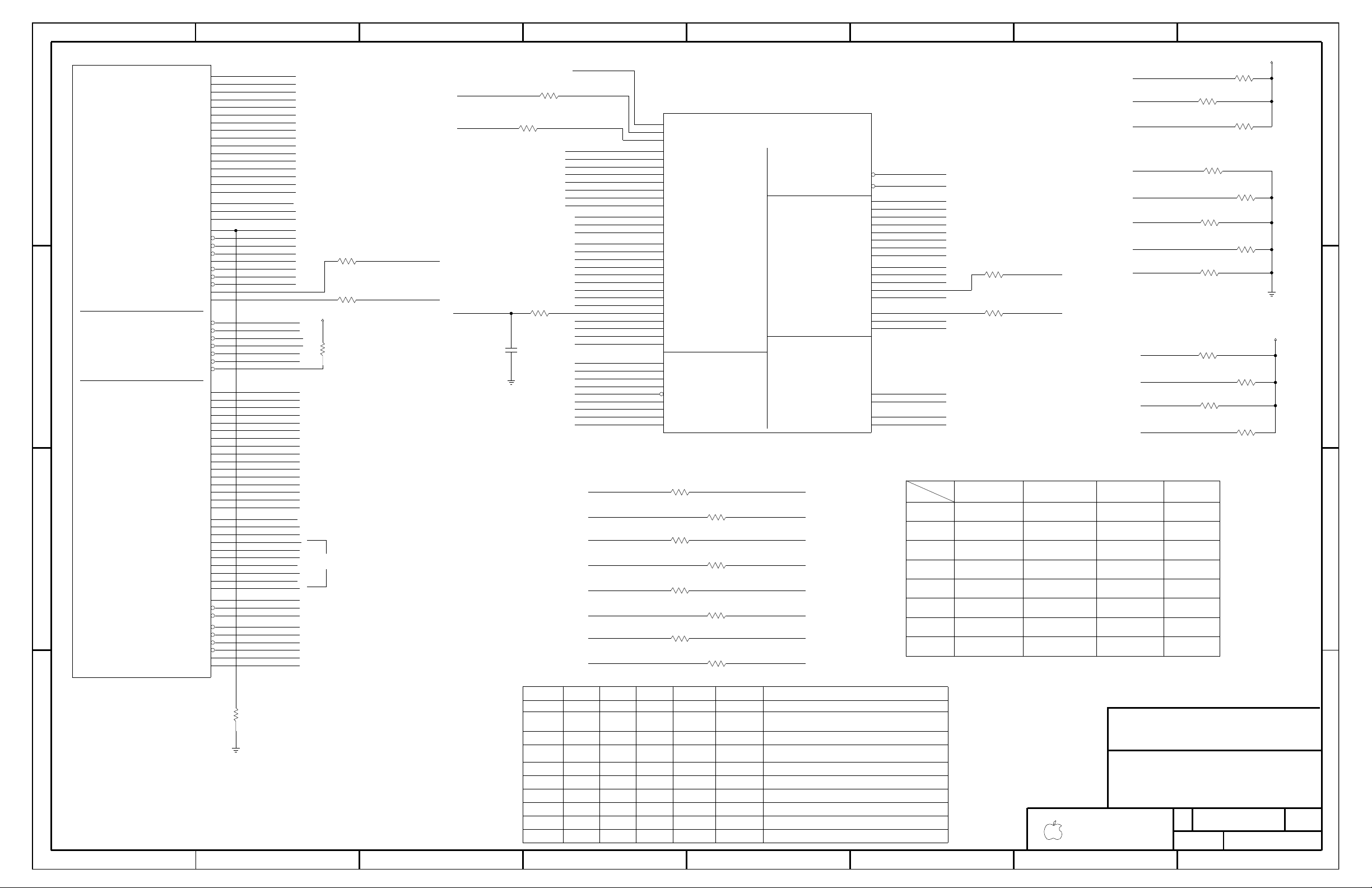
CS_CE2
CS_CE1
CS_IORD
CS_IOWR
ATA_CS1
ATA_CS0
IDE
IDEINTRQ
IDECHRDY
IDECS0
IDECS1
IDEDMACK
IDEDMARQ
IDERD
IDEWR
IDERST
IDEA9
IDEA8
IDEA7
IDEA6
IDEA5
IDEA4
IDEA3
IDEA2
IDEA1
IDEA0
IDEDD15
IDEDD14
IDEDD13
IDEDD12
IDEDD11
IDEDD10
IDEDD9
IDEDD8
IDEDD7
IDEDD6
IDEDD5
IDEDD4
IDEDD3
IDEDD2
IDEDD1
IDEDD0
CARDSLOT
CS_WAIT
CS_OE
CS_WE
ATA_INTRQ
ATA_DMARQ
ATA_CHRDY
ATA_DMACK
ATA_RD
ATA_WR
ATA_RST
ATA_VREF
UATA100
ATA_A1
ATA_A2
ATA_A0
ATA_D12
ATA_D11
ATA_D15
ATA_D14
ATA_D13
ATA_D10
ATA_D9
ATA_D3
ATA_D2
ATA_D1
ATA_D0
ATA_D4
ATA_D8
ATA_D7
ATA_D6
ATA_D5
(5 OF 9)
IICDATA_1
IICCLK_1
IICCLK_0
IICDATA_0
TST_PLLEN
TST_MONOUT
TST_MONIN
TEI
TRSTN
TMS
TCK
TDO
TDI
TEST
MDC
GBE_REFCLK
MDIO
COL
CRS
GTX_CLK
RXD_6
RXD_4
RXD_5
RXD_3
RXD_7
RXD_2
RXD_1
RX_ER
RX_DV
RX_CLK
RXD_0
FW_PINT
FW_LINKON
FWR_LCLK
TX_ER
TX_EN
TX_CLK
TXD_0
RESET
PURESET
PHY_LPS
PHY_CTL0
PHY_CTL1
PHY_LREQ
FWR_PCLK
(4 OF 9)
MISC
TXD_3
TXD_2
TXD_1
TXD_4
TXD_5
TXD_6
TXD_7
GB ETHERNET
FIREWIRE
PHY_DATA0
PHY_DATA1
PHY_DATA2
PHY_DATA3
PHY_DATA5
PHY_DATA7
PHY_DATA4
PHY_DATA6
D
SIZE
OF
SHT
DRAWING NUMBER
NOTICE OF PROPRIETARY PROPERTY
I TO MAINTAIN THE DOCUMENT IN CONFIDENCE
III NOT TO REVEAL OR PUBLISH IN WHOLE OR PART
II NOT TO REPRODUCE OR COPY IT
AGREES TO THE FOLLOWING
PROPERTY OF APPLE COMPUTER, INC. THE POSSESSOR
THE INFORMATION CONTAINED HEREIN IS THE PROPRIETARY
1
2
3
4
5
67
8
12
3
4
5
6
78
B
C
D
A
B
C
D
A
REV.
APPLE COMPUTER INC.
SCALE
NONE
D3-RD
D2-WR
AE-WR
85-RD
N/A
CLOCK SLEW SSCG
ADDR LSB INDICATES READ (’1’) OR WRITE (’0’) MODES
U30 - PG 14
N/A
N/A
U52 - PG 25
LMU
BOOTBANG EEPROM
6A-WR
J2 - PG 25
J25 - PG 11
N/A
5C-WR
6B-RD
RAM - UPPER
N/A N/A
SNAPPER SOUND
N/A
ADDR
A1-RD
BUS
A0-WR
A2-WR
(MAIN)
N/A
N/A
N/A
N/A
(MAIN)
N/A
N/A
N/A
I2C-2
(SLEEP)
N/A
N/A
N/A
N/A
(SLEEP)
PMU
HW_PLL<BIT 0>
TEST PULL-UPS/DOWNS
SELECTED
SELECTED
PLL OUTPUTS
UDMA - STOP
UDMA - HOSTDMARDY/HSTROBE
UDMA - DEVICEDMARDY/DSTROBE
CS_WAIT IS AN INPUT
EIDE/I2C
INT - ENET/FW/UATA
ENET_TXD SERIES TERMINATION
X
(OUTPUT)
ANALYZER_CLK
DDR_
(OUTPUT)
X
TST_PLLEN_H
TPDENABLE
SHUTDOWN
EXTPLL
X
0
0
X
TST_TEI_H
1
1
JTG_RSTN_L
0
0
0
(OUTPUT)
JTG_TDO_H JTG_TDI_H
(I/O)(I/O)
1
1
1
X
HWPLL_
TESTSEL5
(OUTPUT)
0 0
(INPUT)
1
PLL OUTPUTS
10
0(I)
0(I)
MEMWE
SYNC/MEM DATA
BYPASS
0(I)
0(I)
1(I)
1(I)
1(I)
0
0
0(I)
0
0
X
1
0(I)
0(I)
1(I)
1(I)
1(I)
1
1
10
0
0
1(I)
X(I)
X(I)
X(I)
X(I)
X(I)
DESCRIPTION
VIEW PLLS (SOFTWARE)
NORMAL OPERATION
JTAG MODE
ATPG NORMAL
ATPG IDDQ
TEST TRI-STATE
VIEW PLLS (HARDWARE)
FUNCTIONAL TEST WITHOUT
FUNCTIONAL TEST IDDQ
FUNCTIONAL TEST WITH
POSTSCALAR BYPASS
POSTSCALAR BYPASS
NOT USING CARDSLOT INTERFACE
RAM - LOWER
J25 - PG 11
DASH MODEM
J14 - PG 25
N/AN/A
U51 - PG 6
N/A
N/A
N/A
5D-RD
I2C-1
AD-WR
AC-WR
A3-RD
FAN CONTROLLER
N/A
84-WR
AF-RD
(LMU on RUX Brd.)
J3000 - PG 23
I2C-0
I2C PULL-UPS
Keep C847 stub short
21
R259
402
MF
1/16W
5%
1K
81
RP35
SM1
1/16W
5%
10K
2
1
R232
402
MF
1/16W
5%
10K
54
RP16
SM1
5%
1/16W
22
63
RP10
SM1
5%
1/16W
22
81
RP10
SM1
1/16W
5%
22
54
RP10
SM1
5%
1/16W
22
72
RP10
SM1
5%
1/16W
22
63
RP16
SM1
1/16W
5%
22
81
RP16
SM1
5%
1/16W
22
72
RP16
SM1
1/16W
5%
22
+3V_MAIN
12
R269
5%
1/16W
MF
10K
402
21
R270
10K
5%
1/16W
MF
402
2
1
C847
402
CERM
50V
10pF
NO STUFF
5%
+3V_MAIN
+3V_MAIN
21
R263
402
MF
1/16W
5%
1K
72
RP32
2.2K
5%
1/16W
SM1
81
RP32
2.2K
5%
SM1
1/16W
54
RP32
2.2K
SM1
1/16W
5%
63
RP32
2.2K
1/16W
5%
SM1
72
RP35
10K
5%
1/16W
SM1
63
RP35
SM1
10K
5%
1/16W
54
RP35
1/16W
5%
10K
SM1
2
1
R207
1%
1K
1/16W
MF
402
AM2
AJ4
AL2
AA7
AH7
AG8
AE5
AE4
AG2
AD5
AH1
AF2
AG1
AF1
AJ2
AJ1
AG4
AD7
AH2
AF4
AD4
AC5
AM1
AB7
AK4
AG7
AF7
AH5
AK2
AL1
AH4
AG5
AK1
AE7
AF5
AE1
AE2
AC4
AD2
AB5
AB4
AD1
AA1
Y15
Y4
AA2
AA8
AC2
AC1
W8
W2
V1
W1
V2
V4
U2
U1
Y8
W7
Y1
Y2
W5
W4
T1
V5
AB2
AA4
AA5
Y7
AB1
Y5
U51
INTREPID-REV2.1
BGA
CRITICAL
21
R224
402
5%
1/16W
MF
82
21
R205
402
82
MF
1/16W
5%
A5
A7
H9
E10
D9
G10
B7
A6
D8
E9
H10
AR6
AK10
AM7
AN6
AR5
AH10
AT5
AK8
AP5
D2
C4
J12
E8
G9
D7
A4
B4
D6
E7
D3
U5
T2
M2
M1
N4
L2
K2
K1
N5
P7
M4
L4
L1
P5
B5
B6
AM3
AN1
AK5
AN2
H12
L13
N1
N2
T7
U14
E6
C5
U51
BGA
INTREPID-REV2.1
CRITICAL
21
R195
22
5%
1/16W
MF
402
21
R186
402
MF
1/16W
5%
22
21
R149
5%
1/16W
MF
402
10
21
R145
5%
1/16W
MF
402
10
21
R160
5%
MF
402
10
1/16W
C
051-6338
13 40
CLKENET_PHY_GTX
CLKENET_LINK_GTX
JTAG_ENET_TDI
ENET_COL
ENET_LINK_TXD<6>
ENET_LINK_TX_ER
ENET_PHY_TX_EN
HD_DMARQ
ENET_LINK_TXD<5>
ENET_LINK_TXD<3>
INT_I2C_DATA0
EIDE_CS1_L
EIDE_CS0_L
UIDE_DATA<0>
UIDE_DATA<1>
UIDE_DATA<2>
UIDE_DATA<3>
UIDE_DATA<4>
UIDE_DATA<6>
UIDE_DATA<7>
UIDE_DATA<8>
UIDE_DATA<9>
UIDE_DATA<10>
UIDE_DATA<11>
UIDE_DATA<12>
UIDE_DATA<13>
UIDE_DATA<14>
UIDE_DATA<15>
UIDE_DATA<5>
UIDE_ADDR<0>
UIDE_ADDR<1>
UIDE_ADDR<2>
UIDE_REF
UIDE_RST_L
UIDE_DIOW_L
UIDE_DIOR_L
UIDE_DMACK_L
UIDE_IOCHRDY
UIDE_DMARQ
UIDE_INTRQ
CSLOT_OE_L_SPN
NO_TEST=TRUE
CSLOT_WE_L_SPN
NO_TEST=TRUE
CSLOT_IOWAIT_L_PU
EIDE_DATA<0>
EIDE_DATA<3>
EIDE_DATA<5>
EIDE_DATA<4>
EIDE_DATA<7>
EIDE_DATA<6>
EIDE_DATA<8>
EIDE_DATA<10>
EIDE_DATA<9>
EIDE_DATA<12>
EIDE_DATA<11>
EIDE_DATA<13>
EIDE_DATA<15>
EIDE_DATA<14>
EIDE_ADDR<0>
EIDE_ADDR<1>
EIDE_ADDR<2>
CSLOT_ADDR3_SPN
NO_TEST=TRUE
CSLOT_ADDR4_SPN
NO_TEST=TRUE
CSLOT_ADDR5_SPN
NO_TEST=TRUE
CSLOT_ADDR6_SPN
NO_TEST=TRUE
CSLOT_ADDR7_SPN
NO_TEST=TRUE
CSLOT_ADDR8_SPN
NO_TEST=TRUE
CSLOT_ADDR9_SPN
NO_TEST=TRUE
EIDE_IOCHRDY
EIDE_RST_L
EIDE_RD_L
EIDE_WR_L
EIDE_DMARQ
EIDE_DMACK_L
EIDE_INT
CSLOT_IORD_L_SPN
NO_TEST=TRUE
CSLOT_IOWR_L_SPN
NO_TEST=TRUE
UIDE_CS0_L
UIDE_CS1_L
CSLOT_CE1_L_SPN
NO_TEST=TRUE
CSLOT_CE2_L_SPN
NO_TEST=TRUE
FW_PHY_LREQ
CLKFW_PHY_LCLK
INT_I2C_CLK1
INT_I2C_DATA1
INT_I2C_CLK0
ENET_LINK_TXD<6>
ENET_PHY_TXD<6>
ENET_LINK_TXD<7>
ENET_PHY_TXD<7>
ENET_LINK_TXD<5>
ENET_PHY_TXD<5>
ENET_LINK_TXD<2>
ENET_PHY_TXD<2>
ENET_LINK_TXD<4>
ENET_PHY_TXD<4>
ENET_LINK_TXD<3>
ENET_PHY_TXD<3>
ENET_LINK_TXD<0>
ENET_PHY_TXD<0>
ENET_LINK_TXD<1>
ENET_PHY_TXD<1>
INT_PU_RESET_L
INT_RESET_L
JTAG_ASIC_TDI
JTAG_ASIC_TCK
JTAG_ASIC_TMS
JTAG_ASIC_TRST_L
INT_JTAG_TEI
INT_I2C_CLK1
INT_I2C_DATA1
INT_I2C_DATA0
INT_I2C_CLK0
INT_TST_MONOUT_TP
INT_TST_MONIN_PD
ENET_MDC
ENET_MDIO
ENET_CRS
CLKENET_LINK_GBE_REF
ENET_LINK_RXD<7>
ENET_LINK_RXD<6>
ENET_LINK_RXD<5>
ENET_LINK_RXD<4>
ENET_LINK_RXD<2>
ENET_LINK_RXD<3>
ENET_LINK_RXD<1>
ENET_LINK_RXD<0>
ENET_RX_ER
ENET_RX_DV
CLKENET_LINK_RX
CLKFW_LINK_LCLK
FW_PINT
FW_LKON
CLKENET_LINK_TX
ENET_LINK_TX_EN
ENET_LINK_TXD<1>
ENET_LINK_TXD<0>
ENET_LINK_TXD<2>
ENET_LINK_TXD<4>
ENET_LINK_TXD<7>
FW_LINK_DATA<1>
FW_LINK_DATA<3>
FW_LINK_DATA<0>
FW_LINK_DATA<2>
FW_LINK_DATA<4>
FW_LINK_DATA<5>
FW_LINK_DATA<6>
FW_LINK_DATA<7>
FW_PHY_LPS
FW_LINK_CNTL<1>
FW_LINK_CNTL<0>
FW_LINK_LREQ
CLKFW_LINK_PCLK
ENET_PHY_TX_ER
HD_INTRQ
JTAG_ASIC_TDI
JTAG_ASIC_TMS
JTAG_ENET_TDI
JTAG_ASIC_TCK
JTAG_ASIC_TRST_L
INT_JTAG_TEI
INT_TST_MONIN_PD
INT_TST_PLLEN_PD
INT_TST_PLLEN_PD
EIDE_DATA<2>
EIDE_DATA<1>
6
6
6
6
11
13
13
11
13
13
11
11
13
14
14
13
13
13
13
14
14
13
13
13
13
13
26
13
26
13
26
24
13
13
23
24
24
24
24
24
24
24
24
24
24
24
24
24
24
24
24
24
24
24
24
24
24
24
24
24
24
24
24
24
24
24
24
24
24
24
24
24
24
24
24
24
24
24
24
24
24
24
24
24
24
24
24
27
27
25
25
23
13 26
13 26
13 26
13 26
13 26
13 26
13 26
13 26
25
9
13
26
26
26
13
25
25
23
23
13
26
26
26
26
26
26
26
26
26
26
26
26
26
26
26
27
26
13
13
13
13
13
27
27
27
27
27
27
27
27
27
27
27
26
24
13
26
13
26
26
13
13
13
13
24
24
35
35
26
37
37
37
37
37
37
37
39
37
37
37
37
37
37
37
37
37
37
37
37
37
37
37
37
37
37
37
37
37
38
37
37
37
37
37
37
37
37
37
37
37
37
37
37
37
37
37
37
37
37
37
37
37
37
37
37
37
37
37
37
37
37
37
37
35
39
39
39
37 37
37 37
37 37
37 37
37 37
37 37
37 37
37 37
29
29
39
39
39
39
39
39
39
39
39
39
39
37
37
37
35
37
37
37
37
37
37
37
37
37
37
35
35
37
27
35
37
37
37
37
37
37
37
37
37
37
37
37
37
37
27
37
37
37
35
37
37
39
39
26
39
39
39
39
39
39
37
37
Page 14

(PLL9)
(PLL7)
(PLL3)
(PLL2)
(PLL1)
VSSA_8
VSSA4
VSSA3
VSSA2
VSSA1
(PLL9)
(PLL7)
(PLL3)
(PLL2)
(PLL1)
VDD15A_8
VDD15A_4
VDD15A_3
VDD15A_2
VDD15A_1
CPU_INT
PCIPME
EXTINT12
EXTINT13
EXTINT14
EXTINT15
EXTINT16
EXTINT17
GPIO16
GPIO15
GPIO12
GPIO11
GPIO9
GPIO6
GPIO5
GPIO4
GPIO3
GPIO2
GPIO1
GPIO0
VSSU_2
VDDU33_2
VDDU33_1
(6 OF 9)
SCCRTSA
SCCTXDA
SCCDTRA
SCCRXDA
SCCGPIOA
SCCTRXCA
SCCTXDB
SCCGPIOB
SCCTRXCB
SCCRXDB
SCCRTSB
PURPOSE
GENERAL
I/O’S
EXTINT8
EXTINT7
EXTINT6
EXTINT0
INTERRUPTS
EXTINT11
EXTINT4
EXTINT5
EXTINT10
EXTINT9
EXTINT3
EXTINT2
EXTINT1
AUD_DTO
AUD_DTI
AUD_SYNC
MOD_DTO
AUD_BITCLK
AUD_CLKOUT
IICCLK_2
MOD_SYNC
MOD_DTI
MOD_CLKOUT
IICDATA_2
MOD_BITCLK
IIC
AUDIO/I2S
CLOCKS
XTAL_OUT
PROCSLEEPREQ
PENDPROCINT
XTAL_IN
SS_REF_CLK_IN
BUF_REF_CLK_OUT
STOPXTAL
WATCHDOG
PCI_
PCI_
PCI_
VSSU_1
PCI_
USB_VD0_P
USB_VD0_N
USB_VD1_P
USB_VD1_N
USB_VD2_N
USB_VD2_P
USB_PWRFLT0
USB_PRTPWR0
USB_VD3_N
USB_VD3_P
USB
USB_PRTPWR1
USB_PWRFLT1
USB_VD4_N
USB_VD4_P
USB_VD5_N
USB_VD5_P
USB_PRTPWR2
USB_PWRFLT2
ADJ
BYP
GND
OUT
NC
NC
SHDN
IN
CPU0
VDDA
VDD0
VDD1
VDDC
VDDQ
VSS1
VSS0
VSSA
VSSC
VSSQ
LOCK
ODSEL
PD*
SDATA
SCLK
FSEL
CLKIN
RESET*
ADDRSEL
TABLE_11_HEAD
TABLE_11_HEAD
REFERENCE DESIGNATOR(S)
BOM OPTION
QTY
DESCRIPTION
VALUE VOLT. WATT.
TOL.PART #
PACKAGE
DEVICE
TABLE_ALT_ITEM
D
SIZE
OF
SHT
DRAWING NUMBER
NOTICE OF PROPRIETARY PROPERTY
I TO MAINTAIN THE DOCUMENT IN CONFIDENCE
III NOT TO REVEAL OR PUBLISH IN WHOLE OR PART
II NOT TO REPRODUCE OR COPY IT
AGREES TO THE FOLLOWING
PROPERTY OF APPLE COMPUTER, INC. THE POSSESSOR
THE INFORMATION CONTAINED HEREIN IS THE PROPRIETARY
1
2
3
4
5
67
8
12
3
4
5
6
78
B
C
D
A
B
C
D
A
REV.
APPLE COMPUTER INC.
SCALE
NONE
PART NUMBER
ALTERNATE FOR
PART NUMBER
BOM OPTION
REF DES
COMMENTS:
TABLE_ALT_HEAD
-> 1.55V OUTPUT
INT - USB/GPIOS/I2S
1
2
3
4
0
JTG_TDO_H
MOD_SYNC_B_H
MOD_DTO_B_H
MOD_DTI_B_H
MOD_CLKOUT_B_H
MOD_BITCLK_B_H
5
HWPLL_
TESTMUXSEL
SIGNAL NAME
(SIGNAL FROM MODEM)
CBUS_IREQ_L
CBUS_REG_L
INTERNAL 250K PULL-DOWN
OPEN DRAIN OUTPUT
VCORE A/B SEL
MISO
GPIO/EXTINT PULLUPS
INTERNAL 250K PULL-UP
PLACE NEAR INTREPID TO
MINIMIZE OVERSHOOT
INTERNAL 250K PULL-UP
NC
NC
VIA
SCK
ACK*
MOSI
REQ*
POWERBOOK SPARE
USB PORT ASSIGNMENTS
PORT A - PORT D/UNUSED
PORT E/BLUETOOTH
PORT F/MODEM
OUTPUT IMPEDANCE ~18-20 OHMS
NC
PCI INTERRUPTS
CRYSTAL LOAD CAPACITANCE IS 16PF
+3V_MAIN
2
1
C256
10uF
6.3V
20%
805
CERM
21
R166
100K
402
MF
1/16W
5%
+3V_MAIN
2
1
C246
0.1uF
402
10V
20%
CERM
2
1
C235
0.01uF
402
16V
CERM
20%
21
R179
22
1/16W
MF
5%
402
21
R174
402
22
5%
MF
1/16W
21
R192
1/16W
MF
5%
22
402
54
RP13
SM1
47
5%
1/16W
63
RP13
SM1
1/16W
5%
47
81
RP13
SM1
47
5%
1/16W
72
RP13
SM1
1/16W
5%
47
21
R188
5%
MF
1/16W
22
402
V15
U4
AT7
R8
R9
AH29
AK18
AJ16
AJ13
AA15
U8
T8
AG29
P8
N8
K5
L5
M7
M8
H2
H1
G2
G1
L8
L7
N7
J1
K4
M5
J2
J4
AN7
K9
AR4
AF9
AM5
AT4
AG10
AG11
AL5
AN3
AP4
AG9
AF10
AT6
AN8
AJ18
AJ17
AJ12
AA16
AJ7
R1
R2
T4
P1
V8
AH8
AL4
H4
L9
H5
J8
F2
J7
K7
F1
K8
J5
E1
G5
C32
D31
G30
E31
A33
B33
D34
C33
G4
H7
E2
D1
F4
J9
E30
B32
E34
F33
D30
U15
T5
R4
R7
R5
P2
U51
CRITICAL
INTREPID-REV2.1
BGA
+3V_SLEEP
2
1
R193
15K
5%
MF
1/16W
402
2
1
C387
0.22uF
402
20%
6.3V
CERM
21
R201
MF
1/16W
5%
4.7
402
2
1
C386
402
20%
6.3V
CERM
0.22uF
21
R243
402
4.7
5%
1/16W
MF
2
1
C388
0.22uF
402
20%
6.3V
CERM
21
R279
402
4.7
5%
1/16W
MF
2
1
C337
0.22uF
402
20%
6.3V
CERM
2
1
R189
402
5%
1/16W
MF
15K
2
1
C389
0.22uF
402
20%
6.3V
CERM
21
R240
4.7
402
5%
1/16W
MF
21
R280
402
4.7
5%
1/16W
MF
2 1
R144
5%
NO STUFF
10M
1/16W
MF
402
2
1
C151
22pF
402
CERM
5%
50V
2
1
C152
CERM
22pF
402
50V
5%
21
R134
402
0
5%
1/16W
MF
NO STUFF
1
2
3
J9
U.FL-R_SMT
NO STUFF
F-ST-SM
2
1
R113
402
NO STUFF
5%
1/16W
MF
51
2
1
R143
5%
MF
0
402
1/16W
2
1
C721
CERM
20%
603
10V
1uF
2
1
R567
68.1K
MF
402
1/16W
1%
2
1
R574
1/16W
MF
1%
402
18.7K
2
1
C723
CERM
10uF
805
20%
6.3V
21
R568
0
603
MF
1/16W
5%
NO STUFF
21
R565
MF
603
0
1/16W
5%
+2_5V_MAIN
+1_8V_MAIN
5
1
7
6
8
4
3
2
U49
LT1962-ADJ
MSOP
2
1
C392
CERM
20%
0.01uF
16V
402
12
R187
10K
MF
1/16W
5%
402
12
R191
5%
1/16W
MF
10K
402
1
2
R258
1K
402
MF
1/16W
5%
1
2
R241
1K
402
5%
MF
1/16W
45
RP8
10K
1/16W
5%
SM1
18
RP8
5%
1/16W
10K
SM1
63
RP5
SM1
10K
1/16W
5%
54
RP6
5%
1/16W
10K
SM1
63
RP6
SM1
5%
1/16W
10K
72
RP6
SM1
5%
1/16W
10K
36
RP8
SM1
10K
1/16W
5%
27
RP7
SM1
10K
1/16W
5%
36
RP7
SM1
5%
1/16W
10K
45
RP4
5%
1/16W
10K
SM1
81
RP5
SM1
5%
1/16W
10K
81
RP6
10K
1/16W
5%
SM1
36
RP4
5%
1/16W
10K
SM1
27
RP8
5%
1/16W
10K
SM1
2
1
L13
SM
FERR-EMI-100-OHM
+2_5V_MAIN
+3V_MAIN
2
1
L14
SM-1
400-OHM-EMI
SSCG
2
1
C394
0.1uF
20%
10V
402
SSCG
CERM
2
1
L15
400-OHM-EMI
SM-1
SSCG
2
1
C399
SSCG
0.1uF
402
CERM
10V
20%
2
1
C402
603
SSCG
20%
10V
CERM
1uF
21
R293
402
1/16W
MF
33
5%
SSCG
1
2
R292
75
MF
1/16W
5%
402
SSCG
2
1
C400
0.1uF
20%
10V
CERM
402
SSCG
2
1
R288
1/16W
MF
5%
402
10K
SSCG
21
R284
SSCG
MF
1/16W
0
402
5%
2
1
R178
402
5%
1/16W
MF
15K
2
1
R175
15K
MF
1/16W
5%
402
21
R142
5%
402
0
1/16W
MF
SSCG
2 1
R156
10K
402
MF
1/16W
5%
2 1
R157
5%
1/16W
MF
402
10K
2 1
R164
10K
402
MF
1/16W
5%
2 1
R165
10K
402
MF
1/16W
5%
2 1
R182
10K
402
MF
1/16W
5%
2 1
R180
10K
402
MF
1/16W
5%
2 1
R183
5%
1/16W
MF
402
10K
2 1
R181
10K
402
MF
1/16W
5%
21
R250
5%
1/16W
MF
402
10K
45
RP11
10K
1/16W
5%
SM1
36
RP11
1/16W
5%
SM1
10K
27
RP11
SM1
10K
1/16W
5%
18
RP11
10K
1/16W
5%
SM1
1
2
R295
MF
1/16W
5%
10K
NO STUFF
402
1
2
R296
MF
1/16W
5%
10K
402
NO STUFF
21
R153
5%
1/16W
MF
402
10K
2
1
R287
5%
402
MF
10K
1/16W
SSCG
2
1
R286
0
1/16W
MF
402
5%
NO STUFF
21
R218
MF
1/16W
5%
0
402
+3V_SLEEP
21
R746
MF
1/16W
5%
402
10K
21
R158
402
5%
10K
MF
1/16W
21
R148
402
1/16W
MF
5%
10K
+3V_MAIN
15
6
11
19
7
18
5
12
10
1
8
9
17
13
4
2
3
16
20
14
U31
TSSOP
SSCG
CRITICAL
CY28512D
81
RP47
SOFT_MODEM
5%
47
1/16W
SM1
63
RP47
SOFT_MODEM
47
5%
1/16W
SM1
54
RP47
SOFT_MODEM
1/16W
5%
47
SM1
72
RP47
SOFT_MODEM
47
5%
1/16W
SM1
21
R206
USB_MODEM
10K
402
MF
1/16W
5%
72
RP15
USB_MODEM
SM1
5%
1/16W
10K
63
RP15
USB_MODEM
SM1
5%
1/16W
10K
54
RP15
USB_MODEM
5%
1/16W
10K
SM1
81
RP15
USB_MODEM
10K
1/16W
5%
SM1
21
Y2
CRITICAL
8X4.5MM-SM
18.432M
116S1104
1
RES
RES-0402-V2
RESISTOR
10K
1/16W
5%
NO_SSCG
R292
197S0004 197S0035 Y2
Alt. for Siward Part
C
4014
051-6338
CLK18M_INT_XIN
CLK18M_XTAL_IN
INT_EXTINT10_PU
AIRPORT_PCI_INT_L
CBUS_INT_L
+1_5V_INTREPID_PLL3
NEC_PCI_INT_L
+1_5V_INTREPID_PLL2
+1_5V_INTREPID_PLL8
LT1962_INT_BYP
AGP_ATI_INT_L
SND_LIN_SENSE_L
PMU_INT_L
CBUS_INT_L
INT_EXTINT11_PU
MAIN_RESET_L
USB_DDP
USB_DDM
USB_DCP
USB_DCM
USB_DAM
USB_DAP
USB_DBM
USB_DBP
MODEM_USB_DM
USB_DFM
MODEM_USB_DP
USB_DFP
BT_USB_DM
USB_DEM
BT_USB_DP
USB_DEP
VCORE_VGATE
+1_5V_INTREPID_PLL1
+1_5V_INTREPID_PLL4
INT_I2C_CLK2
MPIC_CPU_INT_L
PMU_PME_L
NEC_PCI_INT_L
SND_HP_SENSE_L
INT_EXTINT14_PU
INT_GPIO12_PU
INT_ENET_RST_L
INT_GPIO15_PU
COMM_SHUTDOWN
INT_GPIO1_PU
CG_FSEL
+3V_INTREPID_USB
COMM_TXD_L
COMM_GPIO_L
COMM_DTR_L
PMU_FROM_INT
PMU_ACK_L
INT_EXTINT3_PU
ENET_ENERGY_DET
INT_EXTINT8_PU
PMU_INT_NMI
INT_PEND_PROC_INT
INT_WATCHDOG_L
COMM_TRXC
COMM_RXD
PMU_CLK
PMU_TO_INT
USB_DAM
USB_DAP
USB_DBP
USB_DCP
USB_DCM
USB_OC_AB_L
USB_DDP
USB_DDM
USB_PWREN_CD_L
USB_OC_CD_L
USB_DEP
USB_DEM
USB_OC_EF_L
USB_PWREN_EF_L
INT_EXTINT13_PU
VCORE_VGATE
CLK18M_INT_EXT
INT_REF_CLK_OUT_UF
INT_REF_CLK_OUT
PMU_INT_L
INT_GPIO15_PU
COMM_RING_DET_L
INT_EXTINT8_PU
USB_OC_CD_L
USB_PWREN_AB_L
USB_OC_AB_L
USB_OC_EF_L
USB_PWREN_EF_L
INT_REF_CLK_IN
INT_EXTINT14_PU
INT_EXTINT16_PU
INT_EXTINT12_PU
LTC1962_INT_VIN
LT1962_INT_ADJ
CLK18M_INT_XOUT
CG_CLKOUT
+3V_CG_PLL_MAIN
+2_5V_CG_MAIN
SYSTEM_CLK_EN
INT_REF_CLK_OUT
INT_I2C_CLK1
INT_I2C_DATA1
CG_ADDRSEL
CG_RESET_L
+1_5V_INTREPID_PLL
USB_DFM
USB_DFP
INT_PROC_SLEEP_REQ_L
INT_I2S0_SND_SCLK
INT_I2S0_SND_MCLK
INT_I2S0_SND_LRCLK
INT_I2S0_SND_TO_DAC
COMM_RTS_L
PMU_INT_NMI
PMU_REQ_L
INT_GPIO12_PU
INT_EXTINT13_PU
INT_EXTINT11_PU
INT_EXTINT12_PU
INT_GPIO1_PU
INT_EXTINT16_PU
SYSTEM_CLK_EN
INT_REF_CLK_IN
INT_MOD_CLKOUT
INT_I2C_DATA2
USB_PWREN_CD_L
PMU_REQ_L
USB_DBM
AIRPORT_PCI_INT_L
INT_MOD_DTO
INT_MOD_BITCLK
INT_MOD_CLKOUT_UF
INT_MOD_BITCLK_UF
INT_I2S0_SND_MCLK_UF
INT_MOD_SYNC_UF
INT_MOD_DTI
INT_MOD_DTO_UF
COMM_RING_DET_L
SND_HW_RESET_L
INT_GPIO9_PU
SND_HP_MUTE_L
FW_PHY_PD
SND_AMP_MUTE_L
COMM_RESET_L
INT_I2S0_SND_FROM_ADC
INT_I2S0_SND_LRCLK_UF
SND_HW_RESET_L
INT_MOD_BITCLK_UF
INT_GPIO9_PU
INT_MOD_SYNC
INT_I2S0_SND_SCLK_UF
INT_I2S0_SND_TO_DAC_UF
INT_MOD_CLKOUT_UF
INT_MOD_SYNC_UF
INT_EXTINT3_PU
INT_MOD_DTO_UF
INT_MOD_DTI
USB_PWREN_AB_L
CG_FSEL
CG_LOCK
INT_EXTINT10_PU
39 29 24
39
39
39
39
19
39
39
39
39
38
29
38
29
39
39
38
39
39
29
39
39
24
18
17
39
29
18
18
37 37
37 37
37 37
37 37
33
39
24
17
39
39
33
39
39
39
29
39
39
37
37
33
35
29
25
35
29
35
25
25
12
37
37
39
35
39
39
39
29
29
33
29
35
39
29
24
25
25
25
39
39
39
25
25
35
35
14
14
14
38
14
38
38
19
25
14
14
14
17
14
14
14
14
14
14
14
14
25 14
25 14
25 14
25 14
14
38
38
25
5
17
14
25
14
14
26
14
25
14
14
38
25
25
25
29
29
14
26
14
14
29
29
25
25
29
29
14
14
14
14
14
14
14
14
14
14
14
14
14
14
14
14
35
35
14
14
14
14
14
14
14
14
14
14
14
14
14
14
38
35
14
14
13
13
8
14
14
29
25
25
25
25
25
14
14
14
14
14
14
14
14
14
14
25
25
14
14
14
14
25
25
14
14
14
14
14
14
14
14
25
27
25
25
25
14
14
14
25
14
14
14
14
14
14
14
14
Page 15
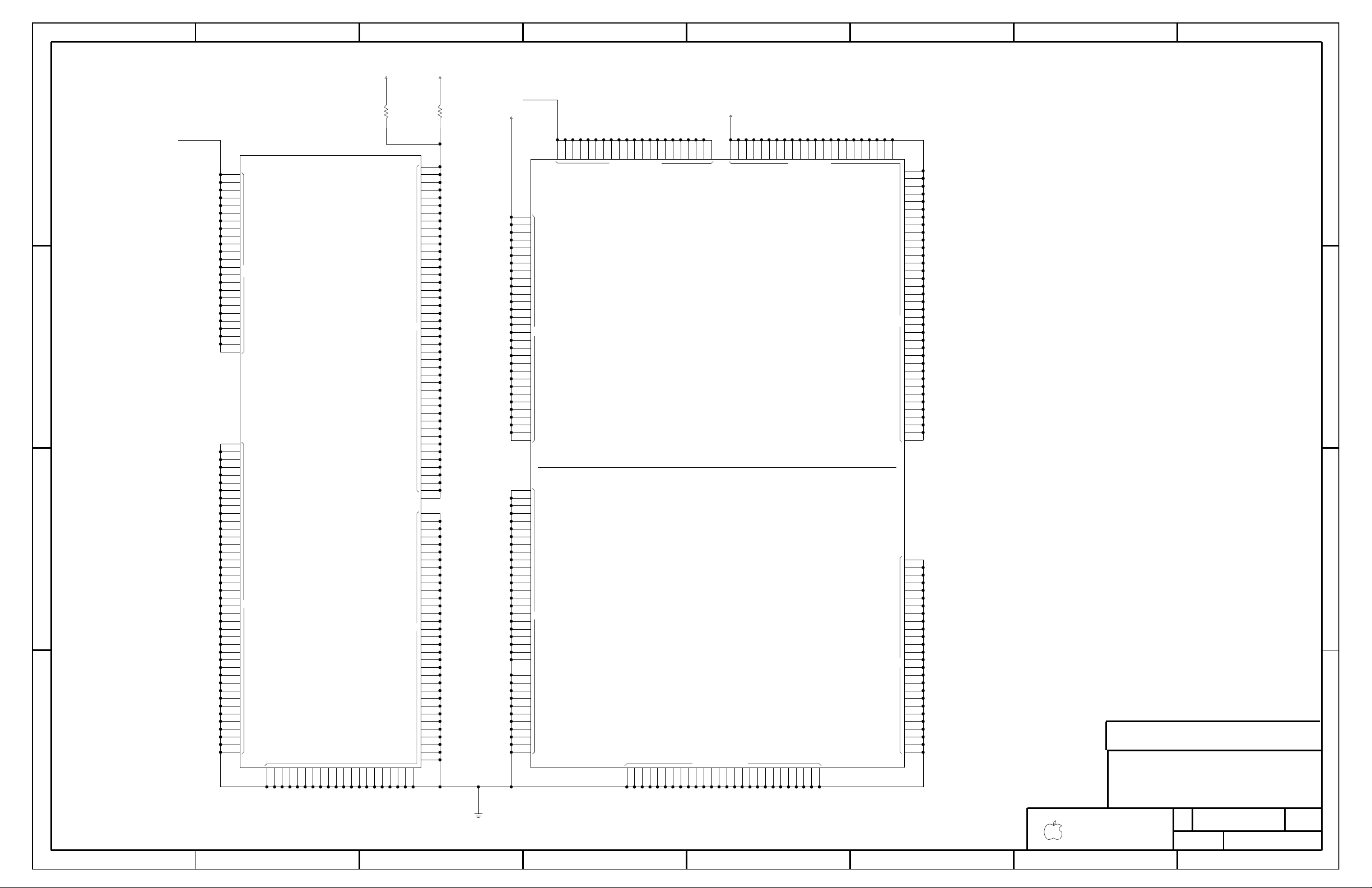
POWER/GROUND
VSS
(8 OF 9)
VDD2.5
VSS
VDD1.8/CPUVIO
GROUND
POWER
(9 OF 9)
VDD1.5
AGP_IO_VDD
VDD3.3
AGP_IO_VSS
VSS
VSS
VDD3.3
D
SIZE
OF
SHT
DRAWING NUMBER
NOTICE OF PROPRIETARY PROPERTY
I TO MAINTAIN THE DOCUMENT IN CONFIDENCE
III NOT TO REVEAL OR PUBLISH IN WHOLE OR PART
II NOT TO REPRODUCE OR COPY IT
AGREES TO THE FOLLOWING
PROPERTY OF APPLE COMPUTER, INC. THE POSSESSOR
THE INFORMATION CONTAINED HEREIN IS THE PROPRIETARY
1
2
3
4
5
67
8
12
3
4
5
6
78
B
C
D
A
B
C
D
A
REV.
APPLE COMPUTER INC.
SCALE
NONE
Intrepid Power
M34
M32
M31
M3
M28
M24
M21
M20
M18
M17
M14
L24
J6
J34
J31
J3G7F6
F34
F31F3F28
F25
F22
F19
F16
F13
F10D4D33C7C36
C34
C31
C3
C28
C25
C22
C19
C16
C13
C10
C1
B35
B2
AT34
AT3
AR35
AR2
AP9
AP6
AP36
AP34
AP33
AP30
AP3
AP27
AP24
AP21
AP18
AP15
AP12
AP1
AN4
AN33
U16
U10
T27
T24
T23
T14
T11
R6
R34
R31
R3
R29
R26
R24
R23
R21
R19
R18
R16
R14
P4
P29
P22
P17
P12
N25
N15
M9
M6
AE31
AC28
AC27
AC25
AB34
E33
Y29
Y27
W34
AB31
W31
W25
V29
V25
U28
U25
T34
T31
T29
T28
AB27
T25
R27
R25
P28
P25
N36
N34
N31
N28
K34
AB25
K31
G34
G31
C35
AP35
AK34
AH34
AH30
AF28
AE34
AA29
AA25
F12
C9
C30
C27
C24
C21
C18
P19
P16
N23
N21
N18
C15
M23
M22
M19
M16
M15
F27
F24
F21
F18
F15
C12
U51
BGA
INTREPID-REV2.1
CRITICAL
AE21
AE19
AE18
AE16
AE14
AD6
AL9
AL6
AL34
AL31
AL27
AD34
AL21
AL18
AL15
AL12
AK7
AK3
AH27
AH23
AH21
AD31
AH20
AG6
AG34
AG30
Y25
Y24
Y23
Y19
Y16
AG3
Y14
Y12
Y11
W26
W23
W14
W11
V6
V34
V31
AG24
V3
V24
V21
V18
V17
V12
V10
U29
U27
U22
AG23
U19
AG21
AE28
AE22
AD3
AD28
G3F9F7
F30
E4
B34
D5
D32
C6
C2
B3
AR3
AC13
AP7
AP2
W6
W3
W13
W12
U12
T6
T3
T18
AC12
T12
R22
P14
P13
N6
N3
N24
K6
K3
AP16
AB6
AP13
AP10
AN5
AM4
AL7
AL3
AL16
AL13
AL10
AK6
AB3
AH6
AH3
AF25
AE6
AE3
AE17
AE15
AD21
AC14
G6
AA12
AA11
AD13
AC23
AC19
AC17
AB19
AB17
AB15
Y18
Y13
W24
W16
V22
V20
V19
V16
U24
U18
AB13
U17
T13
R20
R17
P21
P20
P18
P15
AD22
AD15
AA24
AA21
AA6
AA34
AA31
AA3
AA27
AA20
A34
AD25
AD23
AD12
AC26
AC22
AC20
AC18
AC16A3AC15
AC11
AB29
AB28
AB24
AB18
AB16
AB14
AB12
AB11
AL19
AJ23
AJ21
AH28
AH22
AH19
AF22
AR34
AE23
AR33
AP31
AP28
AP25
AP22
AP19
AN32
AL30
AL28
AL22
AE20
AD20
U51
BGA
INTREPID-REV2.1
CRITICAL
+1_5V_MAIN
+3V_MAIN
2
1
R276
INT_2_5V_COLD
805
FF
1/10W
5%
0
2
1
R274
805
FF
1/10W
5%
0
INT_2_5V_HOT
+2_5V_MAIN
+2_5V_SLEEP
C
051-6338
15 40
+1_5V_AGP
+2_5V_INTREPID
MAXBUS_SLEEP
9
10 16 38
38
38
33
21
16
20
8
19 7 16 6 12
5
Page 16

D
SIZE
OF
SHT
DRAWING NUMBER
NOTICE OF PROPRIETARY PROPERTY
I TO MAINTAIN THE DOCUMENT IN CONFIDENCE
III NOT TO REVEAL OR PUBLISH IN WHOLE OR PART
II NOT TO REPRODUCE OR COPY IT
AGREES TO THE FOLLOWING
PROPERTY OF APPLE COMPUTER, INC. THE POSSESSOR
THE INFORMATION CONTAINED HEREIN IS THE PROPRIETARY
1
2
3
4
5
67
8
12
3
4
5
6
78
B
C
D
A
B
C
D
A
REV.
APPLE COMPUTER INC.
SCALE
NONE
40 X 0.22UF (0402)
INTREPID 3.3V DECOUPLING
INTREPID CORE DECOUPLING
INTREPID AGP I/O DECOUPLING
21 Balls
4 X 10UF (0805)
INTREPID MAXBUS DECOUPLING
INTREPID DDR DECOUPLING
44 Balls
4 X 10UF (0805)
57 Balls
4 X 10UF (0805)
30 Balls
4 X 10UF (0805) 4 X 10UF (0805)
Intrepid Decoupling
29 X 0.22UF (0402)
46 X 0.22UF (0402)
21 X 0.22UF (0402)
24 Balls
28 X 0.22UF (0402)
Place these 2.5V Decoupling Caps near the Edge of +2.5V_MAIN and +2.5V_INTREPID split
INTREPID/MAIN 2.5V DECOUPLING
10 X 0.22UF (0402)
2
1
C178
402
CERM
6.3V
20%
0.22uF
2
1
C182
402
CERM
6.3V
20%
0.22uF
2
1
C204
0.22uF
20%
6.3V
CERM
402
2
1
C166
402
CERM
6.3V
20%
0.22uF
2
1
C142
10uF
20%
6.3V
CERM
805
2
1
C148
805
CERM
6.3V
20%
10uF
2
1
C141
0.22uF
20%
6.3V
CERM
402
2
1
C205
0.22uF
20%
6.3V
CERM
402
2
1
C145
0.22uF
20%
6.3V
CERM
402
2
1
C223
20%
6.3V
CERM
402
0.22uF
2
1
C214
0.22uF
20%
6.3V
CERM
402
2
1
C229
0.22uF
20%
6.3V
CERM
402
2
1
C163
0.22uF
20%
6.3V
CERM
402
2
1
C181
0.22uF
20%
6.3V
CERM
402
2
1
C164
0.22uF
20%
6.3V
CERM
402
2
1
C207
0.22uF
20%
6.3V
CERM
402
2
1
C225
0.22uF
20%
6.3V
CERM
402
2
1
C208
402
0.22uF
20%
6.3V
CERM
2
1
C149
402
CERM
6.3V
20%
0.22uF
2
1
C147
402
CERM
6.3V
20%
0.22uF
2
1
C206
0.22uF
20%
6.3V
CERM
402
2
1
C165
402
CERM
6.3V
20%
0.22uF
2
1
C146
805
CERM
6.3V
20%
10uF
2
1
C144
10uF
20%
6.3V
CERM
805
2
1
C241
402
CERM
6.3V
20%
0.22uF
2
1
C334
402
CERM
6.3V
20%
0.22uF
2
1
C369
0.22uF
20%
6.3V
CERM
402
2
1
C315
402
CERM
6.3V
20%
0.22uF
2
1
C274
0.22uF
20%
6.3V
CERM
402
2
1
C219
402
CERM
6.3V
20%
0.22uF
2
1
C253
402
CERM
6.3V
20%
0.22uF
2
1
C218
0.22uF
20%
6.3V
CERM
402
2
1
C186
402
CERM
6.3V
20%
0.22uF
2
1
C243
402
CERM
6.3V
20%
0.22uF
2
1
C281
402
CERM
6.3V
20%
0.22uF
2
1
C240
0.22uF
20%
6.3V
CERM
402
2
1
C305
402
CERM
6.3V
20%
0.22uF
2
1
C297
20%
6.3V
CERM
402
0.22uF
2
1
C254
402
CERM
6.3V
20%
0.22uF
2
1
C172
402
CERM
6.3V
20%
0.22uF
2
1
C266
0.22uF
20%
6.3V
CERM
402
2
1
C275
0.22uF
20%
6.3V
CERM
402
2
1
C216
402
CERM
6.3V
20%
0.22uF
2
1
C252
402
CERM
6.3V
20%
0.22uF
2
1
C251
0.22uF
20%
6.3V
CERM
402
2
1
C304
0.22uF
20%
6.3V
CERM
402
2
1
C306
0.22uF
20%
6.3V
CERM
402
2
1
C265
402
CERM
6.3V
20%
0.22uF
2
1
C322
10uF
20%
6.3V
CERM
805
2
1
C202
805
CERM
6.3V
20%
10uF
2
1
C314
CERM
805
6.3V
20%
10uF
2
1
C191
10uF
20%
6.3V
CERM
805
2
1
C293
0.22uF
20%
6.3V
CERM
402
2
1
C230
0.22uF
20%
6.3V
CERM
402
2
1
C217
0.22uF
20%
6.3V
CERM
402
2
1
C333
0.22uF
20%
6.3V
CERM
402
2
1
C203
0.22uF
20%
6.3V
CERM
402
2
1
C282
0.22uF
20%
6.3V
CERM
402
2
1
C242
0.22uF
20%
6.3V
CERM
402
2
1
C185
0.22uF
20%
6.3V
CERM
402
2
1
C273
402
CERM
6.3V
20%
0.22uF
2
1
C316
402
CERM
6.3V
20%
0.22uF
2
1
C323
402
CERM
6.3V
20%
0.22uF
2
1
C239
0.22uF
20%
6.3V
CERM
402
2
1
C320
0.22uF
20%
6.3V
CERM
402
2
1
C361
0.22uF
20%
6.3V
CERM
402
2
1
C312
0.22uF
20%
6.3V
CERM
402
2
1
C331
0.22uF
20%
6.3V
CERM
402
2
1
C332
0.22uF
20%
6.3V
CERM
402
2
1
C344
0.22uF
20%
6.3V
CERM
402
2
1
C366
0.22uF
20%
6.3V
CERM
402
2
1
C363
0.22uF
20%
6.3V
CERM
402
2
1
C373
0.22uF
20%
6.3V
CERM
402
2
1
C346
0.22uF
20%
6.3V
CERM
402
2
1
C330
0.22uF
20%
6.3V
CERM
402
2
1
C319
402
CERM
6.3V
20%
0.22uF
2
1
C345
0.22uF
20%
6.3V
CERM
402
2
1
C329
402
CERM
6.3V
20%
0.22uF
2
1
C367
402
CERM
6.3V
20%
0.22uF
2
1
C365
0.22uF
20%
6.3V
CERM
402
2
1
C321
402
CERM
6.3V
20%
0.22uF
2
1
C380
10uF
20%
6.3V
CERM
805
2
1
C379
805
CERM
6.3V
20%
10uF
2
1
C381
805
CERM
6.3V
20%
10uF
2
1
C382
10uF
20%
6.3V
CERM
805
2
1
C290
402
CERM
6.3V
20%
0.22uF
2
1
C300
402
CERM
6.3V
20%
0.22uF
2
1
C222
402
CERM
6.3V
20%
0.22uF
2
1
C236
402
CERM
6.3V
20%
0.22uF
2
1
C224
402
CERM
6.3V
20%
0.22uF
2
1
C258
402
CERM
6.3V
20%
0.22uF
2
1
C302
402
CERM
6.3V
20%
0.22uF
2
1
C263
402
CERM
6.3V
20%
0.22uF
2
1
C287
402
CERM
6.3V
20%
0.22uF
2
1
C248
402
CERM
6.3V
20%
0.22uF
2
1
C292
402
CERM
6.3V
20%
0.22uF
2
1
C250
402
CERM
6.3V
20%
0.22uF
2
1
C303
402
CERM
6.3V
20%
0.22uF
2
1
C238
402
CERM
6.3V
20%
0.22uF
2
1
C260
402
CERM
6.3V
20%
0.22uF
2
1
C262
402
CERM
6.3V
20%
0.22uF
2
1
C279
0.22uF
20%
6.3V
CERM
402
2
1
C226
402
CERM
6.3V
20%
0.22uF
2
1
C288
402
CERM
6.3V
20%
0.22uF
2
1
C278
0.22uF
20%
6.3V
CERM
402
2
1
C310
0.22uF
20%
6.3V
CERM
402
2
1
C299
0.22uF
20%
6.3V
CERM
402
2
1
C301
402
CERM
6.3V
20%
0.22uF
2
1
C271
402
CERM
6.3V
20%
0.22uF
2
1
C325
805
CERM
6.3V
20%
10uF
2
1
C200
10uF
20%
6.3V
CERM
805
2
1
C324
10uF
20%
6.3V
CERM
805
2
1
C201
805
CERM
6.3V
20%
10uF
2
1
C171
402
CERM
6.3V
20%
0.22uF
2
1
C352
402
CERM
6.3V
20%
0.22uF
2
1
C215
402
CERM
6.3V
20%
0.22uF
2
1
C342
402
CERM
6.3V
20%
0.22uF
2
1
C327
402
CERM
6.3V
20%
0.22uF
2
1
C268
402
CERM
6.3V
20%
0.22uF
2
1
C358
0.22uF
20%
6.3V
CERM
402
2
1
C167
402
CERM
6.3V
20%
0.22uF
2
1
C189
402
CERM
6.3V
20%
0.22uF
2
1
C343
0.22uF
20%
6.3V
CERM
402
2
1
C212
0.22uF
20%
6.3V
CERM
402
2
1
C257
0.22uF
20%
6.3V
CERM
402
2
1
C177
0.22uF
20%
6.3V
CERM
402
2
1
C176
402
CERM
6.3V
20%
0.22uF
2
1
C247
0.22uF
20%
6.3V
CERM
402
2
1
C341
0.22uF
20%
6.3V
CERM
402
2
1
C286
402
CERM
6.3V
20%
0.22uF
2
1
C350
402
CERM
6.3V
20%
0.22uF
2
1
C234
0.22uF
20%
6.3V
CERM
402
2
1
C317
0.22uF
20%
6.3V
CERM
402
2
1
C221
0.22uF
20%
6.3V
CERM
402
2
1
C237
0.22uF
20%
6.3V
CERM
402
2
1
C351
402
CERM
6.3V
20%
0.22uF
2
1
C357
0.22uF
20%
6.3V
CERM
402
2
1
C269
0.22uF
20%
6.3V
CERM
402
2
1
C318
20%
6.3V
CERM
402
0.22uF
2
1
C283
402
CERM
6.3V
20%
0.22uF
2
1
C308
402
CERM
20%
6.3V
0.22uF
2
1
C170
0.22uF
20%
6.3V
CERM
402
2
1
C376
805
6.3V
20%
10uF
CERM
2
1
C378
10uF
20%
6.3V
CERM
805
2
1
C175
402
CERM
6.3V
20%
0.22uF
2
1
C285
0.22uF
20%
6.3V
CERM
402
2
1
C360
402
CERM
6.3V
20%
0.22uF
2
1
C375
10uF
20%
6.3V
CERM
805
2
1
C377
805
CERM
6.3V
20%
10uF
2
1
C289
0.22uF
20%
6.3V
CERM
402
2
1
C261
0.22uF
20%
6.3V
CERM
402
2
1
C272
0.22uF
20%
6.3V
CERM
402
2
1
C227
402
CERM
6.3V
20%
0.22uF
2
1
C259
0.22uF
20%
6.3V
CERM
402
2
1
C309
0.22uF
20%
6.3V
CERM
402
2
1
C158
0.22uF
20%
6.3V
CERM
402
2
1
C359
0.22uF
20%
6.3V
CERM
402
2
1
C371
0.22uF
20%
6.3V
CERM
402
2
1
C228
0.22uF
20%
6.3V
CERM
402
2
1
C313
402
CERM
6.3V
20%
0.22uF
2
1
C184
0.22uF
20%
6.3V
CERM
402
2
1
C349
0.22uF
20%
6.3V
CERM
402
2
1
C192
402
CERM
6.3V
20%
0.22uF
2
1
C348
402
CERM
6.3V
20%
0.22uF
2
1
C168
402
CERM
6.3V
20%
0.22uF
2
1
C368
0.22uF
20%
6.3V
CERM
402
2
1
C294
402
CERM
6.3V
20%
0.22uF
2
1
C264
402
CERM
0.22uF
6.3V
20%
2
1
C296
402
CERM
6.3V
20%
0.22uF
2
1
C231
402
CERM
6.3V
20%
0.22uF
2
1
C280
402
CERM
6.3V
20%
0.22uF
2
1
C295
402
CERM
6.3V
20%
0.22uF
2
1
C364
402
CERM
6.3V
20%
0.22uF
2
1
C328
402
CERM
6.3V
20%
0.22uF
2
1
C347
402
CERM
6.3V
20%
0.22uF
2
1
C354
0.22uF
20%
6.3V
CERM
402
2
1
C159
0.22uF
20%
6.3V
CERM
402
2
1
C160
0.22uF
20%
6.3V
CERM
402
2
1
C180
0.22uF
20%
6.3V
CERM
402
2
1
C183
0.22uF
20%
6.3V
CERM
402
2
1
C213
402
CERM
6.3V
20%
0.22uF
2
1
C161
402
CERM
6.3V
20%
0.22uF
2
1
C162
402
CERM
6.3V
20%
0.22uF
2
1
C179
402
CERM
6.3V
20%
0.22uF
+1_5V_MAIN
+3V_MAIN
2
1
C385
402
CERM
6.3V
20%
0.22uF
2
1
C374
0.22uF
20%
6.3V
CERM
402
2
1
C395
CERM
6.3V
20%
0.22uF
402
2
1
C739
402
CERM
6.3V
20%
0.22uF
2
1
C736
402
CERM
6.3V
20%
0.22uF
2
1
C245
402
CERM
6.3V
20%
0.22uF
2
1
C735
402
6.3V
20%
0.22uF
CERM
2
1
C335
402
6.3V
20%
0.22uF
CERM
2
1
C139
0.22uF
20%
6.3V
CERM
402
2
1
C770
20%
6.3V
CERM
402
0.22uF
+2_5V_MAIN
C
16 40
051-6338
+1_5V_AGP
MAXBUS_SLEEP
+2_5V_INTREPID
38
38
33
21
15
20
8
38
19
7
15
15
6
10
12
5
9
Page 17

AVDD
VDD
VDD_PCI
AD3
AD4
AD5
AD2
AD0
AD1
VSS
AD6
AD7
AD17
AD16
AD15
AD8
AD9
AD10
AD11
AD12
AD13
AD14
AD27
AD26
AD25
AD18
AD19
AD20
AD21
AD22
AD23
AD24
AD28
AD29
AD30
AD31
CBE0
CBE1
CBE2
CBE3
PAR
PERR
GNT
DEVSEL
IDSEL
FRAME
IRDY
TRDY
STOP
REQ
SERR
CRUN
SMI
VBBRST
VCCRST
INTA
INTB
INTC
PCLK
PME
LEGC
XT2
DM1
DP1
DM2
DP2
DM3
DP3
RSDM4
RSDM2
RSDP2
RSDM3
RSDP3
RSDP1
XT1/SCLK
RSDM1
DM4
DP4
DM5
DP5
RREF
OCI1
OCI2
OCI4
OCI3
OCI5
RSDP4
RSDM5
RSDP5
PPON1
NC1
NC2
SMC
TEB
NTEST1
PPON2
PPON3
PPON4
PPON5
AVSS(R)
AVSS
SRCLK
SRDTA
SRMOD
NANDTEST
AMC
TEST
D
SIZE
OF
SHT
DRAWING NUMBER
NOTICE OF PROPRIETARY PROPERTY
I TO MAINTAIN THE DOCUMENT IN CONFIDENCE
III NOT TO REVEAL OR PUBLISH IN WHOLE OR PART
II NOT TO REPRODUCE OR COPY IT
AGREES TO THE FOLLOWING
PROPERTY OF APPLE COMPUTER, INC. THE POSSESSOR
THE INFORMATION CONTAINED HEREIN IS THE PROPRIETARY
1
2
3
4
5
67
8
12
3
4
5
6
78
B
C
D
A
B
C
D
A
REV.
APPLE COMPUTER INC.
SCALE
NONE
PART NUMBER
ALTERNATE FOR
PART NUMBER
BOM OPTION
REF DES
COMMENTS:
TABLE_ALT_HEAD
TABLE_ALT_ITEM
Low/Full/High Speed (External)
Low/Full/High Speed (External)
(NEC_USB_DAM)
Y1’s LOAD CAPACITANCE = 16 pF
NEC documentation indicates that NCs must be tied high.
IPD
(PCI_AD<27>)
OD
OD
OD
OD
OD
OD
OUT
OUT
OUT
OUT
IPD
IPD
IPD
IPD
NC
NC
NC
USB 2.0
OUT
IPD
NC
(NEC_USB_DAP)
(NEC_USB_DBM)
(NEC_USB_DBP)
NC
NC
NC
NC
NC
NC
facilitate NAND-tree testing
Series Rpaks required to
NC
NC
Tie to GND (NEC_AVSS_F) at ball N11
402
MF
1/16W
5%
22
2
1
R636
+3V_MAIN
402
MF
1/16W
1%
9.09K
21
R614
SM
FERR-EMI-100-OHM
21
L7
402
CERM
50V
5%
27pF
2
1
C759
402
CERM
50V
5%
27pF
2
1
C136
100
5%
1/16W
MF
402
2
1
R124
CRITICAL
NEC_uPD720101_USB2
FBGA
P8
L9
N2B2A2
B14
H14
N14
P10
N1
D8
F11
J11
G4
D12
H12
L12
M11
B13
N13
B1
C8M4H3
L13
N8E2A3
A12
A13
P12
P3
D7
H4
G12
D13
F13
H13
J13
P2
C9
B8
G1
L8
N7
G3
P9
N9
M9
L6
M7
H1
C14
E14
G14
J12
K13
E13
F12
H11
K14
M14
P11
C6
A9
C10
C11
A11
C12
D9
H2
A8
J4 B9
A10
B10
B11
B12
M8
M6
P6
M10
L7
F4
A7
B7
C7
B3
D6
F3
C13
E12
G13
J14
L14
D14
F14
G11
K12
M13
G2
N6
C3
F1
J3
M2
N11
M12
P13
N12
N10
P7
L1
L2
M1
N3
M3
N4
A6
B6
P4
C5
A5
C4
B5
A4
B4
C1
C2
D2
D1
N5
D3
E1
E3
F2
J1
J2
K3
K1
L3
K2
P5
M5
U17
5%
1/16W
MF
402
10K
21
R606
+3V_MAIN
0.1uF
20%
10V
CERM
402
NO STUFF
2
1
C744
5%
402
MF
1/16W
0
21
R607
0.1uF
20%
402
CERM
10V
NO STUFF
2
1
C743
SM1
1/16W
5%
10K
63
RP43
5%
10K
1/16W
SM1
54
RP43
5%
1/16W
10K
SM1
7
2
RP43
10K
5%
1/16W
SM1
8
1
RP43
SM1
1/16W
47
5%
5
6
7
8
4
3
2
1
RP45
SM1
1/16W
47
5%
5
6
7
8
4
3
2
1
RP44
1/16W
MF
402
5%
0
21
R608
402
MF
1/16W
5%
1K
2 1
R615
402
MF
1/16W
5%
1K
2 1
R632
0
5%
1/16W
MF
603
2
1
R172
1/16W
MF
1%
36
402
21
R613
36
1%
MF
1/16W
402
21
R612
402
36
1%
MF
1/16W
21
R610
36
1%
MF
1/16W
402
21
R609
603
MF
1/10W
5%
0
21
R798
30.0000M
CRITICAL
8X4.5MM-SM
21
Y1
0.1uF
402
CERM
10V
20%
2
1
C749
0.1uF
402
CERM
10V
20%
2
1
C750
0.1uF
402
20%
10V
CERM
2
1
C761
0.1uF
20%
10V
CERM
402
2
1
C752
0.1uF
402
CERM
10V
20%
2
1
C769
0.1uF
402
CERM
10V
20%
2
1
C748
0.1uF
20%
10V
CERM
402
2
1
C756
20%
10V
CERM
402
0.1uF
2
1
C747
402
CERM
10V
20%
0.1uF
2
1
C746
CERM
10V
20%
402
0.1uF
2
1
C765
0.1uF
402
CERM
10V
20%
2
1
C768
10uF
20%
6.3V
CERM
805
C197
402
1/16W
MF
5%
4.7K
2
1
R617
CERM
6.3V
20%
10uF
805
2
1
C173
0.1uF
20%
10V
CERM
402
2
1
C751
0.1uF
402
CERM
10V
20%
2
1
C760
40
051-6338
17
C
197S0038197S0608 Y1
Alt. for Siward Part
NEC_XT2_R
NEC_XT1
NEC_AVSS_F
NEC_AVSS_F
NEC_NANDTESTEN_TP
NEC_OCI<4>
+3V_NEC_VDD
NEC_LEGC
MAIN_RESET_L
NEC_MAIN_RESET_L
NEC_PME_L
NEC_IO_RESET_L
PMU_PME_L
IO_RESET_L
NEC_PCI_INTA_L
NEC_PCI_INTB_L
NEC_PCI_INTC_L
NEC_PCI_INT_L
NEC_LEGC
NEC_CRUN_L
NEC_PME_L
CLK33M_NEC
NEC_MAIN_RESET_L
NEC_IO_RESET_L
NEC_AMC_TP
NEC_OCI<5>
PCI_AD<27>
NEC_RREF
NEC_NANDTESTOUT_TP
NEC_SMI_L_TP
PCI_SERR_L
PCI_PERR_L
NEC_PCI_GNT_L
NEC_PCI_REQ_L
PCI_DEVSEL_L
PCI_STOP_L
PCI_TRDY_L
PCI_IRDY_L
PCI_FRAME_L
PCI_PAR
PCI_CBE<3>
PCI_CBE<2>
PCI_CBE<1>
PCI_CBE<0>
PCI_AD<31>
PCI_AD<30>
PCI_AD<28>
PCI_AD<29>
PCI_AD<25>
PCI_AD<26>
PCI_AD<24>
PCI_AD<23>
PCI_AD<20>
PCI_AD<22>
PCI_AD<21>
PCI_AD<19>
PCI_AD<18>
PCI_AD<17>
PCI_AD<16>
PCI_AD<15>
PCI_AD<14>
PCI_AD<13>
PCI_AD<12>
PCI_AD<11>
PCI_AD<10>
PCI_AD<9>
PCI_AD<8>
PCI_AD<7>
PCI_AD<6>
PCI_AD<5>
PCI_AD<2>
PCI_AD<3>
PCI_AD<4>
PCI_AD<0>
PCI_AD<1>
NEC_IDSEL
NEC_NC<2>
+3V_NEC_VDD
+3V_NEC_VDD
NEC_AVDD
NEC_USB_RSDP1
NEC_LUSB_OCI_UF
NEC_RUSB_OCI
NEC_LUSB_OCI
NEC_XT2
NEC_USB_RSDM2
NEC_USB_RSDM1
NEC_USB_DBP
NEC_USB_DAM
NEC_USB_DBM
NEC_USB_DAP
NEC_USB_RSDP2
NEC_NC<1>
NEC_PPON5_TP
NEC_PPON3_TP
NEC_RUSB_PPON
NEC_LUSB_PPON
NEC_OCI<3>
NEC_PPON4_TP
NEC_RUSB_OCI
NEC_LUSB_OCI
NEC_RUSB_OCI_UF
39
39
39
39
39
39
39
39
39
39
39
39
39
39
39
39
39
39
39
39
39
39
39
39
39
39
39
39
39
39
29
37
39
39
39
39
39
39
37
37
37
37
37
37
37
39
37
39
39
37
37
37
37
37
37
37
37
37
37
37
37
37
37
37
37
37
37
37
37
24
39
24
37
37
37
37
37
37
37
37
37
37
24
24
24
24
24
24
24
37
24
37
37
24
24
24
24
24
24
24
24
24
24
24
24
24
24
24
24
24
24
24
24
19
29
29
18
24
24
24
24
24
24
24
24
24
24
18
18
18
18
18
18
18
24
18
24
24
18
18
18
18
18
18
18
18
18
18
18
18
18
18
18
18
18
18
18
18
39
39
39
39
38
18
24
26
35
12
18
18
18
18
18
18
18
18
18
18
12
12
12
12
12
12
12
18
12
18
18
12
12
12
12
12
12
12
12
12
12
12
12
12
12
12
12
12
12
12
12
38
38
39
37
37
37
37
39
39
39
17
17
17
17
14 17
17
17
14
23
14
17
17
12
17
17
9
18
18
12
12
12
12
12
12
12
12
12
12
12
12
9
9
9
9
9
9
9
12
9
12
12
9
9
9
9
9
9
9
9
9
9
9
9
9
9
9
9
9
9
9
9
17
17
38
25
17
17
25
25
25
25
25
25
17
17
25
Page 18

C/BE3*
C/BE2*
C/BE1*
C/BE0*
VR_EN*
VR_PORT
VCCCB
VCCP
GND
VCC
GRST
MFUNC4
MFUNC5
MFUNC6
MFUNC3
MFUNC0
SUSPEND
MFUNC1
MFUNC2
PCLK
SPKROUT
GNT
TRDY
STOP
FRAME
PRST
REQ
DEVSEL
PERR
IDSEL
SERR
IRDY
AD31
PAR
AD30
AD29
AD28
AD27
AD20
AD21
AD18
AD19
AD26
AD25
AD24
AD23
AD22
AD17
AD10
AD11
AD9
AD8
AD16
AD15
AD14
AD13
AD12
AD7
AD0
AD2
AD3
AD4
AD5
AD6
AD1
D14/RSVD
D13/CAD6
D12/CAD4
D11/CAD2
D10/CAD31
D15/CAD8
D9/CAD30
D8/CAD28
D7/CAD7
D6/CAD5
D5/CAD3
D4/CAD1
D3/CAD0
D2/RSVD
D1/CAD29
D0/CAD27
A22/CTRDY*
A20/CSTOP*
A23/CFRAME*
A21/CDEVSEL*
A19/CBLOCK*
A15/CIRDY*
A14/CPERR*
A12/CC/BE2*
A8/CC/BE1*
A25/CAD19
A24/CAD17
A18/RSVD
A17/CAD16
A16/CCLK
A13/CPAR
A11/CAD12
A10/CAD9
A9/CAD14
A7/CAD18
A6/CAD20
A5/CAD21
CE2/CAD10*
INPACK/CREQ*
WAIT/CSERR*
A4/CAD22
A3/CAD23
A2/CAD24
A1/CAD25
A0/CAD26
VPPD1
VPPD0
VCCD0*
VCCD1*
IORD*/CAD13
IOWR*/CAD15
OE*/CAD11
WE*/CGNT*
CD2*/CCD2*
CD1*/CCD1*
CE1*/CC/BE0*
RDY/IREQ*/CINT*
VS1*/CVS1
VS2*/CVS2
REG*/CC/BE3*
RESET/CRST*
BVD1/CSTSCHG/STSCHG*/RI*
BVD2/SPKR*/CAUDIO
WP/IOIS16*/CCLKRUN*
RI_OUT/PME
CLK_48_RSVD/NC
TPS2211
OC
AVPP
AVCC2
AVCC1
AVCC0
GND
SHTDWN
VCCD0
VCCD1
VPPD0
VPPD1
V_5_2
V_5_1
V_3_2
V_3_1
V_12
D
SIZE
OF
SHT
DRAWING NUMBER
NOTICE OF PROPRIETARY PROPERTY
I TO MAINTAIN THE DOCUMENT IN CONFIDENCE
III NOT TO REVEAL OR PUBLISH IN WHOLE OR PART
II NOT TO REPRODUCE OR COPY IT
AGREES TO THE FOLLOWING
PROPERTY OF APPLE COMPUTER, INC. THE POSSESSOR
THE INFORMATION CONTAINED HEREIN IS THE PROPRIETARY
1
2
3
4
5
67
8
12
3
4
5
6
78
B
C
D
A
B
C
D
A
REV.
APPLE COMPUTER INC.
SCALE
NONE
0.1UF ARE USED TO INCREASE ESD DISCHARGES OF UP TO 10KV
TO MINIMIZE INDUCTANCE!
PC CARD/CARDBUS CONNECTOR
PCI1510 PULL-UPS
CLAMP FOR PC-CARD
CLAMP FOR PCI
NC
NC
NC
CARDBUS
TI REFERENCE SCHEMATIC DID NOT HAVE BULK ON +VCC_CBUS_SW
NC
NC
MAKE SURE VCC AND VPP ARE WIDE PLANE/TRACES
INTEGRATED PULL-UP
(PCI_AD<19>)
+3V_MAIN
+5V_MAIN
20%
10V
CERM
402
0.1uF
2
1
C37
402
10K
1/16W
MF
5%
21
R718
MF
1/16W
10K
402
5%
21
R714
402
10K
1/16W
MF
5%
21
R722
10K
5%
1/32W
25V
SM
1
2
8
9
3
7
4
6
10
5
RP1
20%
6.3V
805
CERM
10uF
2
1
C776
PCI1510GGU
BGA
CRITICAL
A5
D13
B6
A9
B2
L8
D4
M11
K9
L3
L12
N13
B11
N11
N7M1E1D5
C13
A7
J3
N10
L1
M9
L2
M8
D8
C2
A8
A6
G3
K3
G1
N1
G10
L10
N12
M10
K10
L9
N9
K7
K1
C11
F12
B8
F2
L11
C1
N2
M13
K8H4
F13
D1
A11
A2
J1
K2
B4
C5
H12
J10
J13
K12
K11
A3
H11
J12
K13
J11
M12
B3
C4
A4
H10
G13
H13
B5
L13
A1
J2
M3
K6
D6
C6
M2
N4
N5
L6
M6
K4
E3
D3
N6
E4
D2
B1
F4
E2
F3
C3
F1
G4
G2
L7
H2
H3
H1
J4
M4
L5
K5
N3
L4
M5
M7
N8
F11
E11
A12
C9
C8
B12
D10
B9
B10
A10
C12
D11
E10
B7
A13
E13
F10
B13
C10
D12
E12
D9
G12
G11
D7
C7
U8
+2_5V_SLEEP
10K
5%
1/16W
MF
402
2
1
R721
805
CERM
10V
20%
2.2uF
2
1
C796
805
CERM
10V
20%
2.2uF
2
1
C800
20%
CERM
6.3V
4.7uF
805
2
1
C787
10uF
CERM
20%
6.3V
805
2
1
C60
+3V_SLEEP
+3V_SLEEP
CRITICAL
QT500806-L111
M-ST-SM1
9
84
83 82
81
80879
78 77
76 75
74 73
72 71
70
7
69
68 67
66 65
64 63
62 61
60
6
59
58 57
56 55
54 53
52 51
50549
48 47
46 45
44 43
42 41
40
4
39
38 37
36 35
34 33
32 31
30
3
29
28 27
26 25
24 23
22 21
20
2
19
18 17
16 15
14 13
12 11
10
1
J5
0
5%
1/16W
MF
402
2
1
R726
6.3V
402
CERM
20%
0.22uF
2
1
C786
SSOI
6
5
4
3
9
14
15
2
1
16
87
10
13
12
11
U4
CERM
20%
402
6.3V
0.22uF
2
1
C775
CERM
20%
402
6.3V
0.22uF
2
1
C778
402
CERM
20%
6.3V
0.22uF
2
1
C784
CERM
20%
402
6.3V
0.22uF
2
1
C783
402
CERM
20%
6.3V
0.22uF
2
1
C791
47
5%
1/16W
MF
402
21
R724
402
CERM
20%
6.3V
0.22uF
2
1
C789
402
20%
CERM
6.3V
0.22uF
2
1
C782
CERM
20%
10V
402
0.1uF
2
1
C40
402
22
5%
1/16W
MF
2
1
R719
402
MF
1/16W
5%
47
21
R723
18
40
051-6338
C
CBUS_DET_2_L
CBUS_DATA<10>
CBUS_DATA<9>
CBUS_DATA<8>
CBUS_BVD1_L
CBUS_BVD2_L
CBUS_REG_L
CBUS_INPACK_L
CBUS_WAIT_L
CBUS_RESET_L
CBUS_VS2
CBUS_ADDR<24>
CBUS_ADDR<23>
CBUS_ADDR<22>
+VPP_CBUS_SW
+VCC_CBUS_SW
CBUS_ADDR<21>
CBUS_ADDR<20>
CBUS_ADDR<19>
CBUS_ADDR<18>
CBUS_ADDR<17>
CBUS_IOWR_L
CBUS_IORD_L
CBUS_VS1
CBUS_CE2_L
CBUS_DATA<15>
CBUS_DATA<14>
CBUS_DATA<13>
CBUS_DATA<12>
CBUS_DATA<11>
CBUS_DET_1_L
CBUS_ADDR<25>
CBUS_ADDR<8>
CBUS_WP_L
CBUS_DATA<2>
CBUS_DATA<1>
CBUS_DATA<0>
CBUS_ADDR<0>
CBUS_ADDR<1>
CBUS_ADDR<2>
CBUS_ADDR<3>
CBUS_ADDR<4>
CBUS_ADDR<5>
CBUS_ADDR<6>
CBUS_ADDR<7>
CBUS_ADDR<12>
CBUS_ADDR<15>
CBUS_ADDR<16>
+VPP_CBUS_SW
+VCC_CBUS_SW
CBUS_READY
CBUS_WE_L
CBUS_ADDR<14>
CBUS_ADDR<13>
CBUS_ADDR<9>
CBUS_ADDR<11>
CBUS_OE_L
CBUS_ADDR<10>
CBUS_CE1_L
CBUS_DATA<7>
CBUS_DATA<6>
CBUS_DATA<5>
CBUS_DATA<4>
CBUS_DATA<3>
PCI_AD<19>
SLEEP_L_LS5
CBUS_VCCD0_L
CBUS_VCCD1_L
CBUS_VPPD0
CBUS_VPPD1
PCI_AD<26>
CBUS_PCI_IDSEL
PCI_AD<27>
PCI_AD<28>
PCI_AD<29>
PCI_AD<3>
PCI_AD<30>
PCI_AD<31>
PCI_AD<4>
PCI_AD<5>
PCI_AD<6>
PCI_AD<7>
PCI_AD<8>
PCI_AD<9>
PCI_AD<25>
PCI_AD<24>
PCI_AD<23>
PCI_AD<22>
PCI_AD<21>
PCI_AD<20>
PCI_AD<2>
PCI_AD<18>
PCI_AD<17>
PCI_AD<16>
PCI_AD<15>
PCI_AD<14>
PCI_AD<13>
PCI_AD<12>
PCI_AD<11>
PCI_AD<10>
PCI_CBE<0>
PCI_CBE<1>
PCI_CBE<2>
PCI_CBE<3>
PCI_AD<1>
PCI_AD<0>
CLK33M_CBUS
PCI_STOP_L
PCI_TRDY_L
PCI_DEVSEL_L
CBUS_PCI_REQ_L
CBUS_PCI_GNT_L
CBUS_INT_L
CBUS_SUSPEND_PU
CBUS_MFUNC6_PD
CBUS_MFUNC5_PD
CBUS_MFUNC4_PD
CBUS_MFUNC3_PD
CBUS_MFUNC2_PD
CBUS_MFUNC1_PD
PCI_PAR
PCI_IRDY_L
PCI_FRAME_L
PCI_SERR_L
PCI_PERR_L
MAIN_RESET_L
CBUS_ADDR<16>
CBUS_PCI_RESET_L
CBUS_VS2
CBUS_VS1
CBUS_DATA<15>
CBUS_ADDR<0>
CBUS_ADDR<1>
CBUS_ADDR<2>
CBUS_ADDR<3>
CBUS_ADDR<4>
CBUS_ADDR<5>
CBUS_ADDR<6>
CBUS_ADDR<7>
CBUS_ADDR<8>
CBUS_ADDR<9>
CBUS_ADDR<10>
CBUS_ADDR<11>
CBUS_ADDR<12>
CBUS_ADDR<13>
CBUS_ADDR<14>
CBUS_ADDR<15>
CBUS_ADDR_16_UF
CBUS_ADDR<17>
CBUS_ADDR<18>
CBUS_ADDR<19>
CBUS_ADDR<20>
CBUS_ADDR<21>
CBUS_ADDR<22>
CBUS_ADDR<23>
CBUS_ADDR<24>
CBUS_ADDR<25>
CBUS_DATA<0>
CBUS_DATA<1>
CBUS_DATA<2>
CBUS_DATA<3>
CBUS_DATA<4>
CBUS_DATA<5>
CBUS_DATA<6>
CBUS_DATA<7>
CBUS_DATA<8>
CBUS_DATA<9>
CBUS_DATA<10>
CBUS_DATA<11>
CBUS_DATA<12>
CBUS_DATA<13>
CBUS_DATA<14>
CBUS_WAIT_L
CBUS_INPACK_L
CBUS_CE2_L
CBUS_WP_L
CBUS_BVD2_L
CBUS_REG_L
CBUS_RESET_L
CBUS_READY
CBUS_WE_L
CBUS_CE1_L
CBUS_OE_L
CBUS_IOWR_L
CBUS_IORD_L
CBUS_DET_2_L
CBUS_DET_1_L
CBUS_BVD1_L
PCI_PERR_L
CBUS_SUSPEND_PU
PCI_SERR_L
CBUS_MFUNC6_PD
CBUS_MFUNC5_PD
CBUS_MFUNC4_PD
CBUS_MFUNC1_PD
CBUS_MFUNC2_PD
CBUS_MFUNC3_PD
PCI1510_VR_EN_L
+VCC_CBUS_SW
+VPP_CBUS_SW
TPS2211_SHTDWN_L
39
39
39
39
39
39
39
39
39
39
39
39
39
39
39
39
39
39
39
39
39
39
39
39
39
39
39
39
39
39
37
34
37
37
37
37
37
37
37
37
37
37
37
37
37
37
37
39
39
39
37
37
37
37
37
37
37
37
37
37
37
37
37
39
39
39
39
39
39
29
24
33
24
24
24
24
24
24
24
24
24
24
24
24
24
24
24
37
37
37
24
24
24
24
24
24
24
24
24
24
24
37
37
37
37
24
24
37
37
37
37
37
37
24
17
32
17
17
17
17
17
17
17
17
17
17
17
17
17
17
17
24
24
24
17
17
17
17
17
17
17
17
17
17
17
24
24
24
24
17
17
24
24
24
24
24
24
19
39
38
38
39
38
38
12
26
12
12
12
12
12
12
12
12
12
12
12
12
12
12
12
17
17
17
12
12
12
12
12
12
12
12
12
12
12
17
17
17
17
12
12
35
17
17
17
17
17
17
18
18
17
39
39
18
18
38
38
18
18
18
18
18
18
18
18
18
18
18
18
18
18
18
18
18
18
18
18
18
18
18
18
18
18
18
18
18
18
18
18
18
18
18
18
18
18
18
18
18
18
18
18
18
18
18
18
18
18
18
18
18
18
18
18
18
18
18
18
18
18
18
18
9
20
9
9
9
9
9
9
9
9
9
9
9
9
9
9
9
12
12
12
9
9
9
9
9
9
9
9
9
9
9
12
12
12
12
9
9
12
12
12
12
12
12
14
18
18
18
18
18
18
18
12
12
12
17
17
14
18
18
18
18
18
18
18
18
18
18
18
18
18
18
18
18
18
18
18
18
18
18
18
18
18
18
18
18
18
18
18
18
18
18
18
18
18
18
18
18
18
18
18
18
18
18
18
18
18
18
18
18
18
18
18
18
18
18
18
18
17
18
17
18
18
18
18
18
18
18
18
Page 19

XIN/CLKIN
SSCLK
VSS
S0
S1
FRSEL
XOUT
VDD
PAD
THRML
GND
SDA/DK0
SCL/DK1
AGND
PD*
EDGE/HTPLG
DE
HSYNC
VSYNC
IDCK+
IDCK-
D11
D10
D2
D3
D4
D5
D6
D7
D8
D9
D1
D0
GND
GND
AVCC
PVCC2
PVCC1
VCC
AVCC
VCC
EXT_SWING
VREF
TX1+
TX2-
TX1TX2+
TX0+
TX0-
TXC-
TXC+
MSEN
PGND
AGND
PGND
AGND
CTL3/A2
ISEL/RST*
VSS
VSS
(1 OF 6)
RAGE_MOBILITY
AGP_BUSYB
AD_STBB1
AD_STBB0
AD_STB0
AGPREF
AD_STB1
AD30
AD31
AD29
AD28
AD27
AD26
AD25
AD24
AD17
AD14
AD15
AD23
AD22
AD19
AD20
AD21
AD16
AD18
AD6
AD5
AD4
AD13
AD11
AD12
AD10
AD9
AD8
AD7
AD3
CBEB1
CBEB2
CBEB3
AD0
AD1
AD2
CBEB0
PCICLK
FRAMEB
PAR
IRDYB
TRDYB
RSTB
INTAB
GNTB
REQB
DEVSELB
STOPB
MEMVMODE1
MEMVMODE0
TEST_YCLK
TEST_MLCK
D+
D-
VREF
VREFG
MEMTEST
PLLTEST
WBF
ST0
ST1
ST2
SBA5
SBA6
SBA3
SBA4
SBA7
SBA2
STP_AGPB
RBFB
SB_STB
SBA1
SBA0
SUS_STAT
AGPTEST
AGP8X_DETB
RSTB_MSK
DBI_LO
DBI_HI
SB_STBS
VSS VSS
VSSVSS
RAGE_MOBILITY
(2 OF 6)
VDDCI
VSS
(6 OF 6)
RAGE_MOBILITY
OE
GND
OUT
VCC
OSC
D
SIZE
OF
SHT
DRAWING NUMBER
NOTICE OF PROPRIETARY PROPERTY
I TO MAINTAIN THE DOCUMENT IN CONFIDENCE
III NOT TO REVEAL OR PUBLISH IN WHOLE OR PART
II NOT TO REPRODUCE OR COPY IT
AGREES TO THE FOLLOWING
PROPERTY OF APPLE COMPUTER, INC. THE POSSESSOR
THE INFORMATION CONTAINED HEREIN IS THE PROPRIETARY
1
2
3
4
5
67
8
12
3
4
5
6
78
B
C
D
A
B
C
D
A
REV.
APPLE COMPUTER INC.
SCALE
NONE
PART NUMBER
ALTERNATE FOR
PART NUMBER
BOM OPTION
REF DES
COMMENTS:
TABLE_ALT_HEAD
TABLE_ALT_ITEM
(PLACE THE OSCILLATOR AND R304 AND R305
27M OSC
CLOSE TO ATI PIN AJ29)
to SI pin#2
(PLACE C408 CLOSE TO AGPREF PIN)
(PLACE R315 CLOSE TO OSC)
M10 AGP INTERFACE
SPREAD SPECTRUM SUPPORT
S0=1;S1=M => -1.5% DOWN-SPREAD
NC
NC
PLACE VERF VOLTAGE DIVIDER
CLOSE TO ATI M10 VREF PIN
MAIN_RESET_L IS TOGGLED FOR SLEEP
MEMVMODE0=1.8V
FOR 2.5 VDDR1
MEMVMODE1=1.8V
MEMVMODE0=GND
FOR 1.8 VDDR1
MEMVMODE1=GND
NC
(PULL-UP to GPU_MEM_IO)
(SET TO LOW SWING MODE)
Place C879 close
PLL NOISE SHOULD BE LESS THAN 100mV PEAK-TO-PEAK
SIL1162 DVI-Compliant Transmitter
Ext. TMDS source termination
5%
402
MF
47
1/16W
21
R309
402
1/16W
5%
MF
10K
2
1
R337
60-OHM-EMI
SM
21
L22
16V
CERM
20%
0.01uF
402
2
1
C457
10uF
805
6.3V
20%
CERM
2
1
C458
20K
1/16W
402
MF
5%
2
1
R338
20K
5%
1/16W
MF
402
2
1
R335
402
MF
1/16W
1%
45.3
2
1
R372
5%
MF
1/16W
0
402
21
R336
402
5%
10K
MF
1/16W
2
1
R323
ATI_MEMIO_HI
5%
1/16W
MF
402
4.7K
2
1
R371
4.7K
5%
1/16W
MF
402
ATI_MEMIO_HI
2
1
R375
MF
402
1%
1K
1/16W
2
1
R388
1/16W
MF
1K
1%
402
2
1
R397
1/16W
MF
402
1K
1%
2
1
R373
1/16W
MF
402
1K
1%
2
1
R365
402
CERM
20%
10V
0.1uF
2
1
C516
805
10uF
6.3V
CERM
20%
2
1
C508
1/16W
NO STUFF
MF
402
5%
100K
2
1
R304
CERM
4.7uF
6.3V
20%
805
2
1
C401
20%
10V
0.1uF
CERM
402
2
1
C409
SM
FERR-EMI-100-OHM
21
L16
+3V_SLEEP
1/16W
MF
5%
402
0
NO STUFF
2
1
R289
GPU_SS
SM
FERR-EMI-100-OHM
21
L66
+3V_SLEEP
CRITICAL
SOI
CY25811
GPU_SS
8
1
2
7
5
3
4
6
U30
0.1uF
CERM
10V
402
GPU_SS
20%
2
1
C390
10uF
805
CERM
20%
6.3V
GPU_SS
2
1
C384
GPU_SS
MF
0
1/16W
5%
402
2
1
R297
402
5%
MF
1/16W
NO STUFF
0
2
1
R298
0
NO STUFF
402
5%
MF
1/16W
2
1
R290
287
MF
402
1%
1/16W
2
1
R315
1%
MF
402
1/16W
162
2
1
R320
1/16W
402
47
MF
1%
2
1
R313
47K
402
MF
5%
1/16W
2
1
R324
5%
1/16W
MF
402
47K
2
1
R325
1/16W
4.7K
ATI_MEMIO_LO
402
MF
5%
2
1
R376
4.7K
402
MF
1/16W
5%
ATI_MEMIO_LO
2
1
R370
402
MF
1/16W
5%
0
GPU_SS
21
R305
GPU_SS
MF
402
1/16W
33
5%
2
1
R285
0.01uF
CERM
402
16V
20%
2
1
C412
0.01uF
20%
CERM
402
16V
2
1
C476
CERM
402
20%
16V
0.01uF
2
1
C490
0.01uF
402
20%
CERM
16V
2
1
C442
0.01uF
402
20%
CERM
16V
2
1
C530
TSSOP
EXT_TMDS
SIL1162
21
2
22
3
32
33
41
42
38
39
35
36
49
26
27
46
28
45
29
47
48
25
11
12
20
1234
30
44
19
7
8
9
10
13
14
15
16
5
6
17
18
24
40
34
314337
U58
400-OHM-EMI
EXT_TMDS
SM-1
21
L78
EXT_TMDS
SM-1
400-OHM-EMI
21
L79
EXT_TMDS
805
CERM
6.3V
20%
10uF
2
1
C856
400-OHM-EMI
EXT_TMDS
SM-1
21
L80
5%
MF
1/16W
402
EXT_TMDS
10K
2
1
R825
EXT_TMDS
50V
CERM
5%
100pF
402
2
1
C858
CERM
EXT_TMDS
5%
100pF
402
50V
2
1
C860
CERM
805
6.3V
20%
10uF
EXT_TMDS
2
1
C854
10K
5%
1/16W
402
MF
EXT_TMDS
2
1
R823
5%
1/16W
MF
402
10K
NO STUFF
2
1
R818
NO STUFF
402
MF
5%
10K
1/16W
2
1
R824
10K
402
MF
1/16W
5%
NO STUFF
2
1
R819
EXT_TMDS
100pF
5%
50V
402
CERM
2
1
C859
CERM
EXT_TMDS
50V
100pF
5%
402
2
1
C857
CERM
805
EXT_TMDS
6.3V
20%
10uF
2
1
C855
100pF
50V
CERM
402
5%
EXT_TMDS
2
1
C861
5%
EXT_TMDS
50V
CERM
402
100pF
2
1
C862
EXT_TMDS
CERM
805
6.3V
20%
10uF
2
1
C863
22
SM1
1/16W
EXT_TMDS
5%
3
4
2
1
RP56
22
EXT_TMDS
5%
1/16W
SM1
3
4
2
1
RP52
22
EXT_TMDS
SM1
1/16W
5%
3
4
2
1
RP57
22
1/16W
SM1
EXT_TMDS
5%
3
4
2
1
RP53
EXT_TMDS
5%
1/16W
SM1
0K
5
6
7
8
4
3
2
1
RP49
5%
SM1
0
1/16W
INT_TMDS
3
4
2
1
RP58
SM1
1/16W
5%
INT_TMDS
0
3
4
2
1
RP59
5%
1/16W
SM1
0
INT_TMDS
3
4
2
1
RP54
5%
1/16W
SM1
INT_TMDS
0
3
4
2
1
RP55
EXT_TMDS
0K
5%
SM1
1/16W
5
6
7
8
4
3
2
1
RP50
SM1
0K
5%
1/16W
EXT_TMDS
5
6
7
8
4
3
2
1
RP51
EXT_TMDS
1/16W
5%
SM1
0K
5
6
7
8
4
3
2
1
RP60
+3V_SLEEP
CERM
402
10V
20%
0.1uF
2
1
C408
EXT_TMDS
1/16W
402
5%
300
MF
21
R827
300
EXT_TMDS
402
MF
1/16W
5%
21
R828
EXT_TMDS
402
MF
5%
300
1/16W
21
R829
EXT_TMDS
402
1/16W
MF
5%
300
21
R830
402
NO STUFF
CERM
50V
10%
470pF
2
1
C873
NO STUFF
470pF
50V
CERM
402
10%
2
1
C877
NO STUFF
470pF
10%
50V
CERM
402
2
1
C878
CERM
50V
NO STUFF
402
470pF
10%
2
1
C874
NO STUFF
470pF
10%
50V
CERM
402
2
1
C872
402
CERM
50V
10%
470pF
NO STUFF
2
1
C876
NO STUFF
470pF
10%
50V
CERM
402
2
1
C871
50V
CERM
402
10%
NO STUFF
470pF
2
1
C875
CERM
20%
10V
402
EXT_TMDS
0.1uF
21
C864
0.1uF
EXT_TMDS
10V
402
CERM
20%
21
C866
10V
402
EXT_TMDS
0.1uF
20%
CERM
21
C867
EXT_TMDS
10V
402
CERM
0.1uF
20%
21
C865
10K
1/16W
5%
MF
402
EXT_TMDS
2
1
R836
47
5%
1/16W
MF
402
NO STUFF
21
R833
1%
MF
EXT_TMDS
4.99K
402
1/16W
2
1
R837
MF
10K
402
1/16W
5%
NO STUFF
2
1
R835
EXT_TMDS
47
5%
1/16W
MF
402
21
R832
1/16W
MF
402
EXT_TMDS
1K
1%
2
1
R838
402
MF
1K
1/16W
1%
EXT_TMDS
2
1
R839
BGA
CRITICAL
M10-CSP64
64MB
AE27
L1
A22
L2
B22
K1
A23
K2
B23
AC4
AB2
V4
U2
E2
G4
A3
C5
A10
C11
A15
C16
C26
B29
G27
G29
P1
D19
R4
A18
R3
A19
P4
B18
P2
C19
AK3
D8
T28
E8
J6
AJ28
AG29
T27
AE29
AF28
AF30
AD28
AC29
AC28
AB29
AC27
AC30
AD27
AD30
AE28
AD29
AD24
AH30
AF29
AE30
AC22
AG30
R28
B6
B7 C8
T30
AH29
AF27
U27
T29
Y25
Y27
AC11
AC10
W28
U29
R30
N27
AG28
K29
K30
U25
Y29
W29
M28
N29
N28
N30
M30
M27
M29
L28
AB30
AB27
L30
AA29
AB28
AA30
AA27
Y30
AA28
W30
W27
V30
V28
L27
V29
V27
U30
U28
R27
R29
P28
P30
P27
P29
L29
K28
U47
BGA
CRITICAL
64MB
M10-CSP64
G30
N3
N4
N1
N2
M4
L3
M3
L4
K3
K4
J1
J2
H1
H2
B27
A27
D23
C23
D22
C20
D20
C21
D21
C22
A25
B25
A26
B26
AE4
AE3
AD4
AD3
AB4
AB3
AA4
AA3
AD2
AD1
AC2
AC1
AA2
AA1
Y2
Y1
Y4
Y3
W4
W3
U4
U3
T4
T3
W2
W1
V2
V1
T2
T1
R2
R1
G2
G1
F2
F1
D2
D1
C2
C1
J4
J3
H4
H3
F4
F3
E3
E4
B1
A1
B2
A2
B4
A4
B5
A5
D3
C3
D4
C4
D6
C6
D7
C7
A8
B8
A9
B9
A11
B11
A12
B12
C9
D9
C10
D10
C12
D12
C13
D13
A13
B13
A14
B14
A16
B16
A17
B17
C14
D14
C15
D15
C17
D17
C18
D18
C24
D24
C25
D25
C27
D27
C28
D28
B28
A28
A29
A30
C29
C30
D29
D30
E27
E28
F27
F28
H27
H28
J27
J28
E29
E30
F29
F30
H29
H30
J29
J30
AC3
AB1
V3
U1
E1
G3
B3
D5
B10
D11
B15
D16
D26
B30
G28
U47
CRITICAL
M10-CSP64
64MB
BGA
R19
R18
R17
R16
T16
U16
V16
W16
T14
T13
T12
T15
R15
P15
N15
M15
B19
A21
P3
M2
P25
F18
AE15
U6
U47
10V
402
CERM
0.1uF
20%
EXT_TMDS
2
1
C879
+3V_SLEEP
5%
1/16W
402
330
EXT_TMDS
MF
2
1
R826
27MHZ
SM
CRITICAL
14
81
7
G1
19 40
C
051-6338
G1197S0318 197S0048
Alt. for Siward Part
SI_TMDS_D0_STM
SI_TMDS_CLK_STM
TMDS_CLKN
SI_TMDS_D1_STM
SI_MSEN
SI_TMDS_CLKN
SI_TMDS_D2_STM
GPU_DVO_VSYNC
SI_HPD
SI_A2
SI_TMDS_CLKP
TMDS_DP<1>
GPU_TMDS_CLKP
TMDS_DN<0>
+3V_SI_AVCC
+3V_SI_VCC
+3V_SI_PLLVCC
TMDS_DN<0>
TMDS_DP<0>
TMDS_DN<2>
GPU_TMDS_DN<1>
TMDS_CLKP
ATI_DVOD<10>
MAIN_RESET_L
SI_TMDS_DP<0>
SI_TMDS_DN<0>
AGP_AD_STB<1>
AGP_AD<16>
GPU_TMDS_CLKN
SI_TMDS_DP<2>
AGP_SB_STB_L
ATI_DBI_LO_PU
ATI_DBI_HI_PU
ATI_RSTB_MSK
AGP8X_DET_PU
GPU_AGP_TEST
AGP_SUS_STAT_L_PU
AGP_SB_STB
AGP_STP_L
AGP_RBF_L
AGP_SBA<0>
AGP_SBA<1>
AGP_SBA<2>
AGP_SBA<3>
AGP_SBA<4>
AGP_SBA<5>
AGP_SBA<7>
AGP_SBA<6>
AGP_ST<2>
AGP_ST<1>
AGP_ST<0>
AGP_WBF_L
ATI_MEMTEST
AGP_ATI_VREFG
AGP_ATI_VREF
GPU_THERM_DM
GPU_THERM_DP
GPU_MEM_IO
ATI_MEMVMODE1
ATI_MEMVMODE0
AGP_REQ_L
AGP_GNT_L
AGP_PAR
AGP_STOP_L
AGP_FRAME_L
AGP_CBE<0>
CLK66M_GPU_AGP
AGP_CBE<2>
AGP_AD<0>
AGP_CBE<3>
AGP_AD<1>
AGP_AD<2>
AGP_AD<4>
AGP_AD<5>
AGP_AD<6>
AGP_AD<7>
AGP_AD<8>
AGP_AD<10>
AGP_AD<9>
AGP_AD<11>
AGP_AD<12>
AGP_AD<13>
AGP_AD<15>
AGP_AD<14>
AGP_AD<17>
AGP_AD<18>
AGP_AD<19>
AGP_AD<20>
AGP_AD<21>
AGP_AD<23>
AGP_AD<22>
AGP_AD<26>
AGP_AD<25>
AGP_AD<24>
AGP_AD<27>
AGP_AD<28>
AGP_AD<29>
AGP_AD<30>
AGP_AD<31>
INT_AGP_VREF
AGP_AD_STB_L<1>
AGP_BUSY_L
AGP_AD_STB<0>
AGP_AD_STB_L<0>
GPU_VCORE_VDDCI
+3V_GPU
GPU_VCORE
+1_5V_AGP
+3V_GPU
+3V_GPU
GPU_MEM_IO
+3V_GPU
+1_8V_GPU
MAIN_RESET_L
GPU_VCORE_VDDCI
+3V_ATI_SS
ATI_CLK27M_OSC_SS
CY25811_S0
CY25811_S1
ATI_SSCLK_UF
ATI_SSCLK_IN
ATI_DVOD<7>
ATI_DVOD<6>
ATI_DVOD<5>
ATI_DVOD<4>
GPU_DVOD<7>
GPU_DVOD<6>
GPU_DVOD<5>
GPU_DVOD<4>
GPU_DVOD<3>
GPU_DVOD<6>
GPU_DVOD<8>
GPU_DVOD<9>
GPU_DVOD_DE
GPU_DVOD<11>
ATI_DVOD<1>
ATI_DVOD<0>
ATI_DVOD<3>
ATI_DVOD<2>
GPU_DVOD<1>
GPU_DVOD<0>
GPU_DVOD<3>
GPU_DVOD<2>
ATI_CLK27M_IN
ATI_CLK27M_OSC_SS
ATI_DVOD<8>
ATI_DVOD<9>
ATI_DVO_HSYNC
ATI_DVO_VSYNC
ATI_DVOD_DE
ATI_DVO_CLKP
GPU_DVOD<10>
GPU_DVOD<11>
GPU_DVOD<9>
GPU_DVO_HSYNC
GPU_DVO_VSYNC
GPU_DVOD_DE
GPU_DVO_CLKP
SI_TMDS_DP<2>
TMDS_CLKP
TMDS_DP<0>
TMDS_DN<1>
TMDS_DN<0>
TMDS_DP<0>
GPU_TMDS_DN<0>
TMDS_DP<2>
SI_TMDS_DN<2>
TMDS_CLKN
SI_TMDS_CLKN
TMDS_DP<1>
TMDS_DN<1>
SI_TMDS_DP<0>
TMDS_CLKN
TMDS_DN<1>
TMDS_DP<1>
GPU_TMDS_DP<1>
TMDS_DN<2>
TMDS_DP<2>
GPU_TMDS_DN<2>
GPU_TMDS_DP<2>
TMDS_DN<2>TMDS_DP<2>
SI_VREF_IDCK_N
GPU_DVO_CLKP
ATI_DVOD<11>
GPU_DVO_HSYNC
GPU_DVOD<4>
GPU_DVOD<0>
GPU_DVOD<1>
GPU_DVOD<10>
AGP_CBE<1>
AGP_AD<3>
AGP_ATI_RESET_L
AGP_ATI_INT_L
AGP_IRDY_L
AGP_TRDY_L
AGP_DEVSEL_L
SI_TMDS_CLKP
GPU_DVOD<5>
SI_PD_L
SI_I2C_CLK
GPU_DVOD<7>
GPU_DVOD<2>
SI_RST_L
SI_I2S_DATA
SI_TMDS_DN<2>
SI_VREF_IDCK_N
+1_8V_GPU
SI_TMDS_DP<1>
SI_TMDS_DN<0>
SI_TMDS_DP<1>
GPU_DVOD<8>
GPU_TMDS_DP<0>
SI_TMDS_DN<1>
SI_EXT_SWING_SET
TMDS_CLKP
SI_TMDS_DN<1>
ATI_OSC_OE
ATI_CLK27M_OSC
+3V_ATI_OSC_SLEEP
+1_5V_AGP
14 17 18 19 24 29 39
38
39
38
21
29
21
38
20
38
38
38
24
20
39
39
39
39
39
21
19
21
21
21
38
19
39
39
39
39
39
39
39
39
39
39
39
39
39
38
19
37
37
37
37
37
37
37
38
20
39
16
20
20
38
20
21
18
37
37
37
37
37
37
37
37
37
37
37
37
37
37
37 37
21
37
16
22
36
36
36
22
36
22
22
22
22
36
22
36
36
36
37
37
36
36
37
37
37
37
37
37
37
37
37
37
37
21
37
37
37
37
37
37
35
37
37
37
37
37
37
37
37
37
37
37
37
37
37
37
37
37
37
37
37
37
37
37
37
37
37
37
37
37
37
37
37
38
37
37
37
38
19
38
15
19
19
21
19
20
17
38
35
35
36
36
36
36
36
36
36
36
36
36
36
36
36
36
36
36
36
36
36
36
36
36
35
35
36
36
36
36
36
36
36
36
36
36
36
36
36
36
22
22
22
22
22
36
22
36
22 36
22
22
36
22
22
22 36
22
22
36
36
22 22
36
36
36
36
36
36
36
37
37
37
37
37
36
36
36
36
36
20
36
36
36
36
36
36
22
36
15
19
19
19
19
19
20
19
19
19
19
20
19
20
19
19
12
12
20
19
12
12
12
12
12
12
12
12
12
12
12
12
12
12
12
25
25
19
12
12
12
12
12
12
12
12
12
12
12
12
12
12
12
12
12
12
12
12
12
12
12
12
12
12
12
12
12
12
12
12
12
12
12
12
12
12
12
12
12
12
12
12
19
12
20
12
12
12
19
12
19
14
19
38
19
35
20
20
20
20
20
19
19
19
19
19
19
19
19
19
19
20
20
20
20
19
19
19
19
20
19
20
20
20
20
20
20
19
19
19
19
19
19
19
19
19
19
19
19
19
20
19
19
19 19
19
19
19
19
19
19 20
19
19
20
20
19 19
19
19
20
19
19
19
19
19
12
12
14
12
12
12
19
19
20
19
19
20
19
19
19
19
19
19
19
20
19
19
19
35
38
12
Page 20

JUMPER
B00ST
SW
TG
EXT
VCC VCC
INT
VIN
SGND PGND
RUN/SS
BG
VFB
ITH
ION
PGOOD
VRNG
FCB
G
D
S
G
D
S
VDDC
(5 OF 6)
RAGE_MOBILITY
VSS
VDD15
HPD1
DDC3CLK
DDC3DATA
DDC1CLK
DDC1DATA
DDC2CLK
DDC2DATA
BLON
GPIO16
GPIO15
G
R
B
Y_G
R2SET
RSET
H2SYNC
HSYNC
V2SYNC
VSYNC
ZV_LCDDATA5
ZV_LCDDATA4
ZV_LCDDATA3
ZV_LCDDATA2
ZV_LCDDATA6
ZV_LCDDATA15
ZV_LCDDATA14
ZV_LCDDATA13
ZV_LCDDATA12
ZV_LCDDATA7
ZV_LCDDATA8
ZV_LCDDATA9
ZV_LCDDATA10
ZV_LCDDATA11
ZV_LCDDATA16
C_R
DIGON
COMP_B
AUXWIN
ZV_LCDDATA21
ZV_LCDDATA20
ZV_LCDCNTL0
ZV_LCDCNTL1
ZV_LCDDATA22
ZV_LCDDATA23
ZV_LCDDATA17
ZV_LCDDATA18
ZV_LCDDATA19
ZV_LCDCNTL2
ZV_LCDCNTL3
GPIO0
GPIO1
GPIO5
GPIO7
GPIO6
GPIO2
GPIO3
GPIO4
TXOUT_L3N
TXOUT_L2P
TXOUT_L2N
TXOUT_U3P
TXCLK_UN
TXOUT_U2P
TXOUT_L0N
TXOUT_L0P
TXOUT_L1N
TXOUT_L1P
TXOUT_U3N
TXCLK_UP
TXOUT_U2N
TXOUT_U1P
TXOUT_U0P
TXOUT_U0N
TXOUT_U1N
GPIO8
GPIO12
GPIO10
GPIO11
GPIO9
GPIO14
GPIO13
TX0M
TX2P
TX1P
TX2M
TXCM
TX1M
TX0P
TXCP
XTALIN
TXOUT_L3P
TXCLK_LN
TXCLK_LP
SSOUT
XTALOUT
TESTEN
SSIN
ROMCSB
ZV_LCDDATA1
ZV_LCDDATA0
RAGE_MOBILITY
(3 OF 6)
VSS
VSS
VSS
VSS
VSS
D
SIZE
OF
SHT
DRAWING NUMBER
NOTICE OF PROPRIETARY PROPERTY
I TO MAINTAIN THE DOCUMENT IN CONFIDENCE
III NOT TO REVEAL OR PUBLISH IN WHOLE OR PART
II NOT TO REPRODUCE OR COPY IT
AGREES TO THE FOLLOWING
PROPERTY OF APPLE COMPUTER, INC. THE POSSESSOR
THE INFORMATION CONTAINED HEREIN IS THE PROPRIETARY
1
2
3
4
5
67
8
12
3
4
5
6
78
B
C
D
A
B
C
D
A
REV.
APPLE COMPUTER INC.
SCALE
NONE
NC
NC
M10 Power Shut down Sequencing
.
NC
NC
Int.TMDS Termination
NC
M10 CORE PWR/LVDS/TMDS
1.0V = 0.8V * (1 + R329 / R330)
WHEN VCORE_CNTL LOW => 1.0V
WHEN VCORE_CNTL HIGH => 1.2V
1.2V = 0.8V * (1 + R329 / (R328//R330))
NC
NC
GPU VCORE - 1.2V
(GPIO6)
(GPIO5)
(GPIO4)
(GPIO2)
(GPIO0)
NC
NC
NC
NC
NC
NC
NC
(GPIO1)
NC
(GPIO3)
(PUT ALL CAPs BELOW ATI ASIC)
(NO ICT TEST)
(NO ICT TEST)
(NO ICT TEST)
(NO ICT TEST)
(500mA)
NC
NC
Place all TMDS 10 ohms
TRACE SO THAT IT MAY BE CUT BETWEEN CAPS
TERMINATION NETWORK SHOULD BE CONNECTED AS SHOWN
CMF LINE SHOULD BE ROUTED AS 4MIL SURFACE
close to GPU
GPU VCORE SUPPLY
6.3V
402
20%
CERM
0.22uF
2
1
C440
805
6.3V
CERM
10uF
20%
2
1
C484
805
CERM
20%
10uF
6.3V
2
1
C485
0.22uF
6.3V
20%
402
CERM
2
1
C441
0.22uF
6.3V
402
CERM
20%
2
1
C445
6.3V
20%
CERM
402
0.22uF
2
1
C446
0.22uF
CERM
402
6.3V
20%
2
1
C449
402
CERM
20%
6.3V
0.22uF
2
1
C434
0.22uF
20%
CERM
402
6.3V
2
1
C452
20%
CERM
402
6.3V
0.22uF
2
1
C451
CERM
402
20%
6.3V
0.22uF
2
1
C494
0.22uF
402
CERM
20%
6.3V
2
1
C498
0.22uF
20%
6.3V
CERM
402
2
1
C509
20%
CERM
402
6.3V
0.22uF
2
1
C510
20%
CERM
402
6.3V
0.22uF
2
1
C512
CERM
20%
402
0.22uF
6.3V
2
1
C513
6.3V
402
CERM
20%
0.22uF
2
1
C524
0.22uF
6.3V
20%
CERM
402
2
1
C525
0.22uF
CERM
20%
6.3V
402
2
1
C528
6.3V
402
CERM
20%
0.22uF
2
1
C531
0.22uF
20%
CERM
6.3V
402
2
1
C533
6.3V
402
20%
CERM
0.22uF
2
1
C477
6.3V
CERM
402
20%
0.22uF
2
1
C486
6.3V
20%
CERM
402
0.22uF
2
1
C495
OPEN
OMIT
21
XW19
20%
22uF
CERM
1210
10V
2
1
C704
MBRS130LT3
SM
2
1
D29
SOT23
1N914
3
1
D12
25V
0.1uF
603
20%
CERM
2
1
C481
5%
1/16W
MF
603
2.2
21
R358
CERM
20%
603
0.1uF
25V
2
1
C431
603
5%
1/16W
MF
1
2
1
R331
1/16W
402
MF
1%
576K
2
1
R326
4.7uF4.7UF
CERM
20%
10V
1206
2
1
C466
+5V_MAIN
0
402
MF
5%
1/16W
2
1
R343
402
MF
1/16W
1%
20K
2
1
R330
NO STUFF
402
10V
CERM
20%
0.1uF
2
1
C712
GPU_PWRMSR
1/16W
5%
10K
402
MF
21
R549
OMIT
SM
21
XW6
CRITICAL
SSOP
LTC1778
3
10
8
15
14
6
1
2
13
5
7
1149
16
12
U32
402
MF
0
1/16W
5%
NO STUFF
2
1
R344
5%
CERM
402
220pF
25V
2
1
C465
CERM
20%
25V
1206
4.7uF
2
1
C708
+PBUS
1M
MF
1/16W
5%
402
2
1
R327
10V
402
20%
CERM
0.1uF
2
1
C480
402
CERM
50V
10%
470pF
2
1
C455
20K
1%
1/16W
MF
402
2
1
R339
1%
162
MF
1/16W
402
INT_TMDS
2 1
R367
NO STUFF
MF
63.4K
1%
402
1/16W
2
1
R352
402
MF
1/16W
5%
0
2
1
R353
10K
402
MF
5%
1/16W
NO STUFF
2
1
R380
MF
402
1/16W
1%
162
INT_TMDS
2 1
R369
402
50V
10%
470pF
CERM
INT_TMDS
2
1
C507
402
CERM
10%
470pF
50V
INT_TMDS
2
1
C515
1/16W
402
MF
1%
162
INT_TMDS
2 1
R355
MF
402
1/16W
1%
162
INT_TMDS
2 1
R362
10%
470pF
CERM
50V
402
INT_TMDS
2
1
C497
402
CERM
50V
10%
470pF
INT_TMDS
2
1
C487
1%
1/16W
MF
402
162
INT_TMDS
2 1
R340
402
CERM
10%
50V
470pF
INT_TMDS
2
1
C469
470pF
50V
CERM
402
10%
INT_TMDS
2
1
C479
402
1/16W
MF
1%
162
INT_TMDS
2 1
R350
402
MF
1%
162
1/16W
INT_TMDS
2 1
R377
10%
402
50V
470pF
CERM
INT_TMDS
2
1
C522
10%
50V
402
CERM
470pF
INT_TMDS
2
1
C536
1%
MF
402
162
INT_TMDS
1/16W
2 1
R374
4.7uF
20%
25V
CERM
1206
2
1
C706
1/16W
402
MF
5%
100K
2
1
R556
1/16W
100K
5%
402
MF
2
1
R559
BAS16TW
SOT-363
6 1
DP7
2N3904
SM
2
3
1
Q51
2N3904
SM
2
3
1
Q52
10K
5%
1/16W
MF
402
2
1
R558
BAS16TW
SOT-363
52
DP7
SOT-363
BAS16TW
43
DP7
+5V_MAIN
MF
402
1/16W
10K
5%
2
1
R366
5%
402
10K
MF
1/16W
2
1
R368
402
MF
1%
75
1/16W
2
1
R359
75
1%
402
1/16W
MF
NO STUFF
2
1
R341
1%
75
MF
402
1/16W
NO STUFF
2
1
R342
402
MF
1%
75
1/16W
NO STUFF
2
1
R346
1/16W
75
1%
MF
402
2
1
R356
75
1%
1/16W
MF
402
2
1
R360
1%
MF
1/16W
499
402
2
1
R333
402
MF
715
1/16W
1%
2
1
R332
5%
10K
MF
1/16W
402
2
1
R387
NO STUFF
10K
402
5%
MF
1/16W
2
1
R396
5%
402
MF
NO STUFF
10K
1/16W
2
1
R386
5%
MF
10K
1/16W
NO STUFF
402
2
1
R382
1/16W
10K
MF
402
5%
NO STUFF
2
1
R391
NO STUFF
5%
402
MF
10K
1/16W
2
1
R383
NO STUFF
5%
402
MF
10K
1/16W
2
1
R392
5%
10K
402
MF
1/16W
NO STUFF
2
1
R385
NO STUFF
1/16W
MF
402
5%
10K
2
1
R394
1/16W
MF
10K
402
5%
2
1
R384
10K
MF
5%
1/16W
402
NO STUFF
2
1
R393
NO STUFF
5%
10K
MF
402
1/16W
2
1
R381
10K
NO STUFF
1/16W
MF
402
5%
2
1
R390
402
MF
10K
1/16W
5%
NO STUFF
2
1
R395
MF
1K
402
5%
1/16W
2 1
R351
805
CERM
20%
6.3V
10uF
2
1
C411
402
CERM
16V
20%
0.01uF
2
1
C482
402
20%
CERM
16V
0.01uF
2
1
C435
402
CERM
20%
16V
0.01uF
2
1
C443
20%
CERM
402
0.01uF
16V
2
1
C448
CERM
402
16V
0.01uF
20%
2
1
C526
0.01uF
402
20%
CERM
16V
2
1
C529
402
20%
16V
CERM
0.01uF
2
1
C532
0.01uF
16V
20%
CERM
402
2
1
C505
4.99K
1%
1/16W
MF
402
2
1
R329
1/16W
MF
402
5%
INT_TMDS
10K
2
1
R389
FERR-220-OHM
0805
21
L17
MF
402
5%
100K
1/16W
2
1
R357
33K
5%
1/16W
MF
402
2
1
R555
CRITICAL
TSOP
SI3446DV
4
36
5
2
1
Q23
1000pF
10%
25V
X7R
402
2
1
C407
SOT-363
BAS16TW
52
DP5
SOT-363
BAS16TW
43
DP5
BAS16TW
SOT-363
61
DP5
+2_5V_SLEEP
SM
21
XW11
SM
21
XW12
SM
21
XW5
SM
21
XW9
SM
21
XW4
402
5%
1/16W
MF
1K
21
R378
402
MF
1/16W
5%
10
INT_TMDS
21
R760
10
5%
1/16W
MF
402
INT_TMDS
21
R764
402
MF
1/16W
5%
10
INT_TMDS
21
R763
402
MF
1/16W
5%
10
INT_TMDS
21
R762
10
5%
1/16W
MF
402
INT_TMDS
21
R761
MF
10
5%
1/16W
402
INT_TMDS
21
R767
5%
1/16W
10
MF
402
INT_TMDS
21
R765
MF
1/16W
5%
10
402
INT_TMDS
21
R766
5%
1/16W
MF
402
10K
2
1
R779
SOT-363
2N7002DW
4
5
3
Q25
2N7002DW
SOT-363
1
2
6
Q25
402
1/16W
5%
100K
MF
2
1
R786
+5V_MAIN
IRF7832
SO-8
CRITICAL
321
4
8765
Q49
SI7860DP
SO-8-PWRPK
CRITICAL
321
4
5
Q48
NO STUFF
402
CERM
50V
20%
0.001uF
2
1
C838
GPU_PWRMSR
18.2K
1%
1/16W
MF
402
2
1
R328
1%
MF
402
GPU_PWRMSR
1.82K
1/16W
2
1
R361
GPU_PWRMSR
10V
CERM
402
0.1uF
20%
2
1
C846
6.3V
330uF
20%
CASE-D4
TANT
CRITICAL
2
1
C705
6.3V
330uF
20%
CASE-D4
TANT
CRITICAL
2
1
C707
6.3V
20%
CASE-D4
TANT
CRITICAL
330uF
2
1
C711
MF
1/16W
10K
5%
402
EXT_TMDS
2
1
R840
SM
CRITICAL
2.1uH-11A
3
2
1
L64
BGA
M10-CSP64
64MB
CRITICAL
G16
G15
AD23
G14
AD22
AD21
AD20
AD19
AD18
AD17
AD16
AD15
AD14
AD13
G13
AD12
AD11
AD10
AD9
AD8
AD7
AC24
AC23
AC8
AC7
G12
AB24
AB7
AA24
AA7
Y24
Y7
W24
W7
V24
V7
G11
U24
U7
T24
T7
R24
R7
P24
P7
N24
N7
G10
M24
M7
L24
L7
K24
K7
J24
J7
H24
H23
G9
H8
H7
G24
G23
G22
G21
G20
G19
G18
G17
G8
G7
AD26
P6
H6
G6
F6
AF5
V25
W25
N25
M25
F25
AE24
F24
AH4
F23
AE18
AC25
AE17
AF15
W26
AF14
AE14
F14
F13
AG4
AE11
F11
AE10
F10
F7
AE6
AD6
AC6
W6
V6
AF25
AJ3
AB25
R25
G25
F17
AB6
T6
L6
F12
U47
BGA
M10-CSP64
64MB
CRITICAL
AK7
AJ7
AH7
AG7
AK6
AJ6
AH6
AH11
AG11
AK10
AJ10
AG6
AH10
AG10
AK9
AJ9
AH9
AG9
AK8
AJ8
AH8
AG8
AK5
AJ5
AG5
AH5
AK4
AJ4
AK23
AJ30
AJ29
AG27
B21
A20
A24
B20
B24
AG25
AG22
AH22
AG20
AH20
AG19
AH19
AG18
AH18
AJ20
AK20
AJ18
AK18
AJ17
AK17
AJ16
AK16
AK12
AJ12
AG21
AH21
AJ19
AK19
AK15
AJ15
AK14
AJ14
AK13
AJ13
AH24
AJ25AJ26
AK25
AE5
AJ24
AK28
AG26
AF11
AG24
AF3
AG3
AH1
AF4
AJ1
AH2
AH3
AK1
M1
AE1
AE2
AF1
AG1
AF2
AG2
AK2
AJ2
AK27
AE13
AH26
AH25
AE12
AF12
AH28
AH27
AK24
AK22
AF13
AK26
AJ27
U47
C
051-6338
20 40
GPU_VCORE_SW_F
GPU_VCORE_SW
GPU_HPD
GPU_TMDS_CLKN
GPU_TMDS_DN<0>
GPU_TMDS_DN<1>
GPU_TMDS_DN<2>
GPU_TMDS_D2_CMF
GPU_TMDS_D1_CMF
GPU_TMDS_DP<2>
+GPU_VDD15_NECK
1778_ITH
1778_BG
1778_TG
1778_VCC
+3V_GPU
GPU_TMDS_CLKN ATI_TMDS_CLKN
GPU_TMDS_CLKP ATI_TMDS_CLKP
GPU_TMDS_DN<1>
GPU_TMDS_DP<1> ATI_TMDS_DP<1>
GPU_TMDS_DN<2> ATI_TMDS_DN<2>
GPU_TMDS_DP<2> ATI_TMDS_DP<2>
ATI_TMDS_DP<0>
1778_SHDN_L
DCDC_EN
GPU_VCORE_SEQ
SLEEP_L_LS5
GPU_VCORE_SEQ_L
GPU_VCORE_PWR_SEQ
+1_5V_AGP
+3V_GPU
GPU_VCORE_NECK
+1_8V_ATI_PVDD
+1_8V_PVDD_NECK
+1_5V_AGP_NECK
ATI_AGP_FBSKEW<0>
1778_GND
+1_5V_AGP
GPU_CORE_OK
1778_GND
1778_VRNG
ATI_BUS_CFG<1>
ATI_AGP_FBSKEW<1>
+3V_GPU
ATI_X1CLK_SKEW<0>
1778_ITH_RC
1778_BST_RC
1778_BST
ATI_BUS_CFG<2>
ATI_BUS_CFG<0>
GPU_VCORE
+GPU_VDD15_UF
+2_5V_SLEEP_NECK1
+1_5V_AGP
1778_VIN
1778_ION
GPU_VCORE_CNTL_L
GPU_VCORE_CNTL
1778_VFB
HIGH_VCORE_DIVD
GPU_VCORE
HIGH_VCORE
GPU_VCORE_CNTL_RC
1778_VFB
GPU_TMDS_DP<0>
GPU_TMDS_DN<0>
+GPU_VDD15_UF
ATI_TMDS_DN<0>
ATI_X1CLK_SKEW<1>
1778_FCB
GPU_TMDS_D0_CMF
GPU_TMDS_CLKP
GPU_CORE_OK
SI_I2C_CLK
SI_I2S_DATA
GPU_DVI_DDC_CLK
GPU_DVI_DDC_DATA
LVDS_DDC_CLK
LVDS_DDC_DATA
INV_ON_PWM
ATI_SSCLK_IN
GPU_VCORE_CNTL_L
GPU_G
GPU_R
GPU_B
ATI_VSYNC
ATI_HSYNC
GPU_Y
ATI_RSET
ATI_R2SET
GPU_COMP
GPU_C
FP_PWR_EN
AUXWIN_PU
LVDS_U0N
LVDS_U0P
LVDS_U2N
LVDS_U1N
LVDS_U1P
LVDS_U3N_TP
LVDS_U3P_TP
CLKLVDS_UP
CLKLVDS_UN
LVDS_L0N
LVDS_L0P
LVDS_L1N
LVDS_L2N
LVDS_L1P
LVDS_L2P
LVDS_L3N_TP
CLKLVDS_LP
LVDS_L3P_TP
CLKLVDS_LN
ATI_DVOD<2>
ATI_DVOD<3>
ATI_DVOD<4>
ATI_DVOD<5>
ATI_DVOD<7>
ATI_DVOD<6>
ATI_DVOD<8>
ATI_DVOD<9>
ATI_DVOD<10>
ZV_LCDDATA20_PU
ATI_DVO_VSYNC
ATI_DVO_HSYNC
ATI_DVOD_DE
ATI_DVO_CLKP
ATI_X1CLK_SKEW<0>
ATI_AGP_FBSKEW<0>
ATI_AGP_FBSKEW<1>
ATI_X1CLK_SKEW<1>
ATI_BUS_CFG<0>
ATI_BUS_CFG<1>
ATI_BUS_CFG<2>
ATI_GPIO7_SPN
ATI_GPIO9_SPN
ATI_GPIO8_PD
ATI_GPIO10_SPN
ATI_GPIO12_SPN
ATI_GPIO11_SPN
HPD_PWR_SNS_EN
ATI_GPIO13_SPN
ATI_TMDS_DP<0>
ATI_TMDS_DN<1>
ATI_TMDS_DN<0>
ATI_TMDS_DP<1>
ATI_TMDS_DP<2>
ATI_TMDS_CLKP
ATI_CLK27M_IN
ATI_TESTEN
ATI_DVOD<0>
ATI_DVOD<1>
GPU_VCORE
+1_5V_GPU_VDD15
LVDS_U2P
ATI_TMDS_DN<2>
ATI_TMDS_CLKN
ATI_TMDS_DN<1>
GPU_TMDS_DP<0>
GPU_TMDS_CLK_CMF
GPU_TMDS_DP<1>
+3V_GPU
ATI_DVOD<11>
+1_8V_GPU
19 20 36
38
38
38
21
21
21
38
34
20
38
20
38
20
38
21
33
19
21
19
21
39
19
39
39
21
36
36
36
36
20
36
36
36
36
36
36
33
32
16
20
16
20
38
16
39
38
39
36
36
36
39
39
39
39
39
39
39
39
38
36
36
20
38
20
20
20
20
19
20 37
20 37
20
20 37
20
37
20
37
37
32
26 15
19
38
38
15
21
38
19
20
38
15
38
20
38
20
20
38
37
20
21
39
39
35
37
37
37
37
37
37
37
37
37
37
37
37
37
37
37
36
36
36
36
36
36
36
36
36
36
36
36
36
37
37
37
37
37
37
35
36
36
20
37
37
37
37
20
20
19
36
21
38 38
22
19
19
19
19
38
38
38
38
38
12
19 20
19 20
19
19 20
19 20
19 20
20
28
18 12
12
38
21
38
38
20
20
12
20
20
38
20
20
12
20
38
38
38
20
20
19
20
38
12
38
38
20
20
19
20
19
19
20
20
20
38
19
20
19
19
22
22
22
22
22
19
20
22
22
22
22
22
22
22
22
22
22
22
22
22
22
22
22
22
22
22
22
22
22
22
22
19
19
19
19
19
19
19
19
19
19
19
19
19
20
20
20
20
20
20
20
22
20
20
20
20
20
20
19
19
19
19
38
22
20
20
20
19
19
12
19
19
Page 21

JUMPER
CONT
NOISE
VIN
VOUT
GND
CONT
NOISE
VIN
VOUT
GND
VDDR1
DVOVMODE
LVDDR_25
LVDDR_25
VSS2DI
VSS1DI
VDD2DI
VDD1DI
(4 OF 6)
RAGE_MOBILITY
PVSS
AVSSQ
AVSSN1
AVSSN0
A2VSSQ
A2VSSN0
A2VSSN1
VSSRH0
VSSRH1
VDDR1
A2VDD0
A2VDD1
PVDD
AVDD1
AVDD0
A2VDDQ
VDDRH0
VDDRH1
VDDP
LPVSS
TPVSS
MPVSS
LVSSR0
LVSSR1
LVSSR2
LVSSR3
VDDM
LVDDR_18
LVDDR_18
LPVDD
TPVDD
MPVDD
TXVDDR3
TXVDDR0
TXVDDR1
TXVDDR2
TXVSSR3
TXVSSR2
TXVSSR1
VDDR3
VDDR4
D
SIZE
OF
SHT
DRAWING NUMBER
NOTICE OF PROPRIETARY PROPERTY
I TO MAINTAIN THE DOCUMENT IN CONFIDENCE
III NOT TO REVEAL OR PUBLISH IN WHOLE OR PART
II NOT TO REPRODUCE OR COPY IT
AGREES TO THE FOLLOWING
PROPERTY OF APPLE COMPUTER, INC. THE POSSESSOR
THE INFORMATION CONTAINED HEREIN IS THE PROPRIETARY
1
2
3
4
5
67
8
12
3
4
5
6
78
B
C
D
A
B
C
D
A
REV.
APPLE COMPUTER INC.
SCALE
NONE
1.8V DVO POWER (EXT.TMDS)
3.3V IO SUPPLY
AGP 4X I/O - 1.5V
1.8V
GPU PLL - 1.8V
(1200mA)
(20mA)
(150mA MAX)
(150mA MAX)
(140mA)
MEMORY CORE - 2.5V
MEMORY I/O
(1800mA)
(AVDD+VDDDI=75mA)
(20mA)
(2mA)
(AVDD+VDDDI=75mA)
M10 POWER
2.5V1.8V
2.5V
(350mA)
(180mA)
(21mA)
(40mA)
3.3V
LVDS - 2.5V
1.5V
GPU POWER SOURCES - 1.5V, 1.8V, 2.5V & 3.3V
LVDS/TMDS - 1.8V
LVDS PLL - 1.8V
MEMORY PLL - 1.8V
(Max Current varies, depends on usage)
2
1
C488
10V
CERM
402
20%
0.1uF
2
1
C456
CERM
0.1uF
402
10V
20%
2
1
C421
CERM
10V
20%
0.1uF
402
2
1
C544
0.1uF
CERM
402
10V
20%
2
1
C545
0.1uF
20%
402
CERM
10V
2
1
C551
20%
10uF
805
6.3V
CERM
2
1
C546
20%
10V
402
CERM
0.1uF
2
1
C422
CERM
10uF
20%
805
6.3V
2
1
C424
0.1uF
CERM
402
10V
20%
2
1
C417
16V
402
CERM
20%
0.01uF
2
1
C547
20%
10V
402
CERM
0.1uF
2
1
C540
0.1uF
CERM
402
10V
20%
2
1
C437
0.1uF
402
CERM
10V
20%
2
1
C436
0.1uF
CERM
10V
20%
402
2
1
C423
0.1uF
10V
402
CERM
20%
2
1
C444
0.1uF
20%
CERM
10V
402
2
1
C425
16V
CERM
20%
402
0.01uF
2
1
C447
20%
16V
CERM
402
0.01uF
2
1
C438
0.1uF
20%
402
CERM
10V
2
1
C439
402
20%
16V
0.01uF
CERM
2
1
C517
20%
10V
402
CERM
0.1uF
2
1
C543
10V
0.1uF
CERM
402
20%
2
1
C541
0.1uF
CERM
402
10V
20%
2
1
C542
20%
16V
0.01uF
CERM
402
2
1
C483
10uF
20%
CERM
805
6.3V
2
1
C419
0.1uF
CERM
402
10V
20%
2
1
C420
16V
402
20%
0.01uF
CERM
2
1
C475
0.1uF
402
10V
CERM
20%
2
1
C504
402
16V
CERM
20%
0.01uF
2
1
C538
16V
20%
CERM
402
0.01uF
2
1
C539
CERM
402
10V
20%
0.1uF
2
1
C470
CERM
0.1uF
402
10V
20%
2
1
C471
402
20%
16V
0.01uF
CERM
2
1
C489
0.1uF
CERM
402
20%
10V
2
1
C496
20%
0.1uF
CERM
10V
402
2
1
C506
16V
20%
0.01uF
402
CERM
2
1
C492
0.1uF
CERM
402
10V
20%
2
1
C501
CERM
402
20%
16V
0.01uF
2
1
C450
402
CERM
20%
16V
0.01uF
2
1
C453
402
20%
0.01uF
CERM
16V
2
1
C473
16V
CERM
20%
402
0.01uF
2
1
C500
402
0.01uF
16V
20%
CERM
2
1
C430
20%
10V
402
CERM
0.1uF
2
1
C460
CERM
16V
402
0.01uF
20%
2
1
C463
0.01uF
402
20%
CERM
16V
2
1
C462
0.01uF
16V
20%
CERM
402
2
1
C454
16V
CERM
20%
402
0.01uF
2
1
C472
CERM
402
20%
16V
0.01uF
2
1
C527
CERM
402
20%
16V
0.01uF
+1_5V_SLEEP
2
1
R275
5%
FF
0
805
1/10W
+2_5V_SLEEP
2
1
R319
ATI_MEMIO_HI
0
5%
1/10W
FF
805
+3V_SLEEP
2
1
R379
805
FF
1/10W
5%
0
+1_8V_SLEEP
2
1
R312
ATI_MEMIO_LO
805
1/10W
5%
0
FF
2
1
C468
CERM
16V
402
20%
0.01uF
2
1
C523
20%
0.01uF
16V
CERM
402
2
1
R363
FF
1/10W
805
5%
0
+1_8V_SLEEP
+2_5V_SLEEP
+2_5V_SLEEP
2
1
C413
402
0.01uF
16V
20%
CERM
2
1
C464
CERM
20%
6.3V
805
10uF
2
1
C478
10uF
805
6.3V
20%
CERM
2
1
C461
402
0.01uF
CERM
20%
16V
2
1
C459
20%
805
CERM
6.3V
10uF
2
1
C511
CERM
10uF
805
6.3V
20%
2
1
C427
6.3V
805
CERM
20%
10uF
2
1
C493
6.3V
10uF
805
20%
CERM
2
1
C537
6.3V
10uF
805
20%
CERM
2
1
C499
10uF
805
6.3V
20%
CERM
2
1
C414
10V
0.1uF
402
CERM
20%
2
1
C418
10uF
20%
805
CERM
6.3V
2
1
C514
10uF
20%
6.3V
CERM
805
2
1
C491
20%
10V
CERM
402
0.1uF
21
L23
FERR-220-OHM
0402
21
L21
FERR-220-OHM
0402
21
L24
0402
FERR-220-OHM
21
L28
0402
FERR-220-OHM
21
L20
FERR-220-OHM
0402
21
L19
0402
FERR-220-OHM
21
L32
0402
FERR-220-OHM
21
L30
FERR-220-OHM
0402
21
L29
FERR-220-OHM
0402
2
1
C552
805
CERM
6.3V
20%
10uF
21
L25
0805
FERR-220-OHM
21
L26
SM
FERR-10-OHM-500MA
21
L31
0805
FERR-220-OHM
21
XW7
OMIT
OPEN
21
L18
SM
FERR-10-OHM-500MA
51
4
2
3
U34
MM1571J
CRITICAL
SOT-25A
2
1
C553
402
20%
16V
CERM
0.01uF
2
1
C830
20%
CERM
10V
603
1uF
+2_5V_SLEEP
51
4
2
3
U60
MM1571J
CRITICAL
SOT-25A
2
1
C833
20%
603
1uF
10V
CERM
2
1
C834
16V
20%
0.01uF
CERM
402
2
1
C835
10uF
805
20%
6.3V
CERM
21
L75
0402
FERR-220-OHM
2
1
C831
805
6.3V
20%
10uF
CERM
2
1
C832
402
CERM
16V
20%
0.01uF
2
1
R787
0
5%
1/16W
MF
402
2
1
R788
402
MF
1/16W
5%
0
2
1
C519
402
20%
10V
0.1uF
CERM
2
1
C534
0.1uF
402
CERM
20%
10V
2
1
C535
20%
CERM
805
6.3V
10uF
2
1
C521
0.1uF
CERM
402
10V
20%
2
1
C550
CERM
6.3V
20%
10uF
805
2
1
C518
402
10V
20%
0.1uF
CERM
2
1
C520
402
20%
10V
CERM
0.1uF
2 1
L33
SM
FERR-10-OHM-500MA
21
L81
FERR-10-OHM-500MA
SM
EXT_TMDS
21
R842
MF
1/16W
5%
0
EXT_TMDS
402
2
1
C881
402
CERM
10V
20%
0.1uF
2
1
C880
20%
10V
CERM
402
0.1uF
2
1
C426
20%
10V
CERM
0.1uF
402
2
1
R841
402
MF
1/16W
5%
0
INT_TMDS
2
1
R843
603
0
5%
1/16W
MF
INT_TMDS
M6
F20
AF19
AG23
N6
F19
AE8
AF7
AE7
AF6
AE25
AD25
AF10
AF9
AE9
AF8
AF26
AE26
R5
P5
N5
M5
L5
E25
E24
E23
E22
E21
E17
E16
K5
E15
E14
E11
E10
E9
H26
E7
J26
J25
H25
J5
F22
F21
F16
F15
F9
F8
AA6
Y6
R6
K6
H5
G26
AD5
AC5
AB5
AA5
Y5
W5
V5
U5
T5
G5
F5
N26
M26
L26
K26
AA25
K27
Y28
T25
AC26
AB26
AA26
Y26
V26
U26
T26
R26
P26
L25
K25
F26
E26
E20
E19
E18
E13
E12
E6
E5
AF20
AH23
AH15
AH14
AH13
AG15
AG14
AG13
AG12
AJ11AK11
AK30AK29
A6A7
AF18
AH17
AG17
AH16
AF17
AG16
AF16
AE16
AJ21AK21
AH12
AF22
AE23
AE22
AF24
AF23
AJ22
AE20
AE19
AJ23
AF21
AE21
U47
BGA
64MB
M10-CSP64
CRITICAL
C
051-6338
21 40
+1_8V_GPU
GPU_MEM_IO_FLT
+1_8V_GPU
+1_8V_ATI_PVDD
GPU_MEM_IO
+2_5V_GPU
+2_5V_GPU
+2_5V_GPU
+3V_GPU
GPU_MEM_IO
+2_5V_GPU
+1_8V_GPU
+1_8V_GPU_VDDDI
+1_8V_GPU
+2_5V_GPU_MCLK
+2_5V_GPU
+1_8V_ATI_PVDD
+1_8V_GPU
+1_8V_GPU_AVDDQ
+1_5V_AGP
+1_5V_AGP
GPU_CORE_OK
ATI_PVDD_BYP
GPU_CORE_OK
+1_8V_GPU_TP_PLL
+2_5V_GPU_A2VDD
ATI_TPVDD_BYP
+1_8V_ATI_PVDD
1_8V_PVDD_STD
+1_8V_ATI_TPVDD
1_8V_TPVDD_STD
+3V_GPU
+1_8V_GPU
+1_8V_GPU
GPU_MEM_IO
+1_5V_AGP_GPU
ATI_DVOVMODE
+2_5V_GPU_PNLIO
+1_8V_GPU_VDDDI
+1_8V_GPU_AVDD
+1_8V_GPU_PLL
+2_5V_GPU_A2VDD
+1_8V_GPU_AVDDQ
+2_5V_GPU_MCLK
+2_5V_GPU_MEMCORE
+1_8V_GPU_PNLPLL
+1_8V_GPU_MEMPLL +1_8V_GPU_TP_PLL
+1_8V_GPU_PNLIO
+1_8V_GPU_DVO
+3V_GPU_FLT
12
12
15
15
12
16
16
12
19
19
19
19
19
19
19
19
19
19
19
20
20
20
19
20
19
20
20
20
20
20
20
20
20
20
20
19
21
21
21
21
21
21
21
21
21
21
21
21
21
21
21
21
21
21
21
21
20
20
21
21
21
21
21
21
21
21
21
21
21
21
38
38
38
38
38
38
38
38
38
38
38
38
38
38
38
38
38
38
38
38
38
21
21
38
38
38
38
38
38
38
38
38
38
38
38
38
38
38
38
38
38
38
38
38
38
Page 22

G2
D2
S2
G1
S1
D1
G
SD
G
SD
G
SD
G
D
S
G
DS
MINIDIN
S
D
G
A
B
Y
32
32
SYM_VER-1
SYM_VER-1
SYM_VER-1
SYM_VER-1
CRITICAL BOM OPTION
TABLE_5_HEAD
PART#
DESCRIPTION
QTY
REFERENCE DESIGNATOR(S)
TABLE_5_ITEM
D
SIZE
OF
SHT
DRAWING NUMBER
NOTICE OF PROPRIETARY PROPERTY
I TO MAINTAIN THE DOCUMENT IN CONFIDENCE
III NOT TO REVEAL OR PUBLISH IN WHOLE OR PART
II NOT TO REPRODUCE OR COPY IT
AGREES TO THE FOLLOWING
PROPERTY OF APPLE COMPUTER, INC. THE POSSESSOR
THE INFORMATION CONTAINED HEREIN IS THE PROPRIETARY
1
2
3
4
5
67
8
12
3
4
5
6
78
B
C
D
A
B
C
D
A
REV.
APPLE COMPUTER INC.
SCALE
NONE
EXTERNAL VIDEO (DVI) INTERFACE
PLACE L1002 & L1003 CLOSE TO DVI CONNECTOR
when system is running.
COMPARATOR ENABLED BY NV17MAP
(55mA requirement per DVI spec)
ANALOG FILTERING
PLACE CLOSE TO CONNECTOR
S-VIDEO/COMP OUT INTERFACE
INVERTER INTERFACE
VGA SYNC BUFFERS
graphics controller
Panel has 2K pull-ups
100K pull-ups are for
LVDS INTERFACE
(LVDS DDC POWER)
NC
Place GND shorts at
graphics controller
Place GND shorts at
(TMDS_DN<5>)
will turn off, as will remote
As host rails rise, TP0610
device path into DDC_CLK.
Isolation will be disabled as well.
on, driving SOFT_PWR_ON_L low.
will be low, TP0610 will turn
NV17M DURING SHUTDOWN. WHEN
Power key detect path when
is pressed, 5V will be driven
power key on remote device
system is shutdown or asleep..
into DDC_CLK. Since host rails
DDC_CLK is isolated from
3V LEVEL SHIFTERS
NC
NC
NC
NC
(+5V_DDC SLEEP)
GPIO.
Power key detect path
HPD will be driven to 5V.
on remote device pressed,
3.3V. When power key
HPD normally driven to
pullup.
on when DVI monitor
powered DDC clock
Pulldown prevents
has active, self-
3904 from turning
VIDEO CONNECTORS
INVERTER EXPECTS ACTIVE HIGH SIGNAL
DVI POWER SWITCH
(TMDS_DN<4>)
(TMDS_DP<4>)
(TMDS_DP<3>)
NC
LCD INTERFACE
(TMDS_DP<5>)
PLACE NEAR C5A & C5B
PLACE NEAR 3, 11 & 19
no-panel case (development)
(TMDS_DN<3>)
NC
Isolation required for DVI power switch
LCD POWER SWITCH
TMDS FILTERING
PLACE CLOSE TO CONNECTOR
NOTE: Pulldown for DVI_HPD provided by DVI power switch interface
DVI DDC CURRENT LIMIT
+5V_MAIN
2
1
R750
402
MF
1/16W
100K
5%
2
1
C816
0.001uF
CERM
50V
402
20%
CHGND3
2
1
C815
402
50V
20%
0.001uF
CERM
2
1
C812
50V
0.001uF
20%
CERM
402
2
1
C813
6.3V
20%
CERM
805
10uF
12
L73
SM
FERR-1K-OHM-EMI
21
L72
400-OHM-EMI
SM-1
+PBUS
+3V_MAIN
2
1
C22
402
CERM
10V
20%
0.1uF
4
3
2
6
Q76
FDG6324L
SC70-6
1
5
6
Q76
FDG6324L
SC70-6
21
L49
SM
0.068uH
2
1
C641
402
50V
0.25%
3.3pF
CERM
2
1
C634
402
50V
0.25%
CERM
3.3pF
2
1
C631
402
50V
0.25%
3.3pF
CERM
21
L43
SM
0.068uH
2
1
C642
4.7pF
50V
CERM
5%
402
21
L40
0.068uH
SM
2
1
C635
4.7pF
5%
402
CERM
50V
21
L50
SM
0.068uH
2
1
C632
4.7pF
402
5%
50V
CERM
21
L44
0.068uH
SM
21
L41
0.068uH
SM
2
1
R474
402
MF
1/16W
5%
10K
2
1
R480
10K
5%
1/16W
MF
402
1
2
6
Q39
2N7002DW
SOT-363
+3V_SLEEP
4
5
3
Q39
2N7002DW
SOT-363
2
1
R481
100K
5%
1/16W
MF
402
2
1
C655
100pF
201
25V
5%
CERM
2
1
R476
4.7K
5%
1/16W
MF
402
2
1
R478
5%
1/16W
402
MF
4.7K
2
1
C654
100pF
5%
25V
201
CERM
2
1
C667
20%
50V
0.01uF
CERM
603
21
L42
400-OHM-EMI
SM-1
4
5
3
Q40
2N7002DW
SOT-363
21
F2
CRITICAL
SM
0.5AMP-13.2V
21
D19
SM
MBR0530
2
1
C653
100pF
201
25V
CERM
5%
21
R475
10K
5%
402
MF
1/16W
2
1
C668
20%
10V
CERM
402
0.1uF
2
1
R485
402
68.1K
1%
1/16W
MF
2
5
1
3
4
U42
LMC7211
SM
21
R472
10K
1%
1/16W
MF
402
2
1
R484
100K
1%
1/16W
MF
402
2
1
R482
1/16W
10K
1%
402
MF
1
2
6
Q40
SOT-363
2N7002DW
2
1
R483
470K
5%
402
MF
1/16W
21
R460
10K
5%
402
MF
1/16W
2
1
R459
5%
330
402
MF
1/16W
2
1
3
Q38
SM
TP0610
2
1
C657
0.01uF
CERM
50V
20%
603
CHGND1
CHGND1
2
1
C656
10%
560pF
402
CERM
50V
21
L54
FERR-10-OHM-500MA
SM
21
L53
0603
3.3uH
21
L57
0603
3.3uH
2
1
C660
10%
560pF
402
50V
CERM
2
1
C658
10%
560pF
402
50V
CERM
2
1
C659
0.01uF
603
20%
50V
CERM
21
L55
0603
3.3uH
21
L56
FERR-10-OHM-500MA
SM
2
1
C663
10%
560pF
CERM
50V
402
2
1
C661
10%
560pF
402
50V
CERM
2
1
C664
10%
560pF
402
CERM
50V
+3V_SLEEP
+5V_SLEEP
21
XW15
SM
21
XW14
SM
21
R479
100
5%
402
1/16W
MF
21
R477
100
402
MF
1/16W
5%
21
R469
100
402
MF
1/16W
5%
4
3
2
1
6
5
J4
SM-2MT
CRITICAL
21
L74
400-OHM-EMI
SM-1
5
4 3
2 1
1110
98
J21
CRITICAL
RT-TH
MH11773-WMR8A
CHGND4
2
1
C548
0.001uF
402
CERM
50V
20%
2
1
R543
100K
5%
1/16W
MF
402
2
1
C701
0.001uF
20%
50V
CERM
402
CHGND4
+3V_SLEEP
2
1
R544
100K
5%
1/16W
MF
402
CHGND4
2 1
C549
20%
50V
CERM
402
0.001uF
CHGND4
2
1
C503
0.001uF
402
CERM
50V
20%
21
L27
FERR-250-OHM
SM
+3V_MAIN
21
C474
603
5%
50V
CERM
2200pF
4
3 6
5
2
1
Q29
TSOP
SI3443DV
21
R354
402
MF
1/16W
100K
5%
2
1
R347
402
MF
1/16W
5%
100K
2
1
3
Q28
2N7002
SM
2 1
R473
680
402
MF
1/16W
5%
CHGND1
CHGND3
21
C819
0.01uF
603
CERM
50V
20%
9
8
7
6
5
4
3
24
23
22
21
20
2
19
18
17
16
15
14
13
12
11
10
1
36
35
34
33
32
31
C5B C5A
C4
C3
C2
C1
J22
QH1112
F-RT-TH
CRITICAL
21
R753
0
5%
1/16W
MF
402
9
8
7
6
5
4
30
3
29
28
27
26
25
24
23
22
21
20
2
19
18
17
16
15
14
13
12
11
10
1
34
33
J14
CRITICAL
G-501973
F-RT-SM
4
5
3
2
1
U2
SC70
NC7S32
2
1
C702
NO STUFF
0.001uF
20%
50V
CERM
402
2
1
R470
MF
402
5%
330
1/16W
2
1
R462
402
MF
1/16W
75
1%
2
1
R458
402
1%
75
1/16W
MF
2
1
R456
1%
75
1/16W
MF
402
21
L36
0402
FERR-60-OHM-0.1A
OMIT
21
L38
FERR-60-OHM-0.1A
0402
OMIT
+3V_MAIN
5
4
2
1
3
U40
74AHC1G32
SM
+3V_MAIN
5
4
2
1
3
U39
SM
74AHC1G32
2
1
L1
FERR-250-OHM
SM
2
1
C19
0.001uF
402
50V
20%
CERM
CHGND2
CHGND1
CHGND2
2 1
R464
402
MF
1/16W
5%
0
2 1
R463
MF
1/16W
5%
0
402
1
6
2
Q35
MMDT3904
SOT-363
4
3
5
Q35
SOT-363
MMDT3904
4
32
1
L37
SM
370-OHM
4
32
1
L46
90-OHM-300mA
2012H
CRITICAL
4
32
1
L47
2012H
90-OHM-300mA
CRITICAL
4
32
1
L45
2012H
90-OHM-300mA
CRITICAL
116S1331
VGA_BUFFER_RESL36,L38
2
DISCRETE,RES,33OHM,0402
C
4022
051-6338
DVI_DDC_DATA_UF
TMDS_CONN_DP<0>
TMDS_CONN_DN<0>
TMDS_DN<0>
TMDS_DP<0>
TMDS_CONN_CLKP
TV_COMP
TV_GND2
+5V_DDC_SLEEP_UF
+5V_DDC_SLEEP
TMDS_CLKP
TMDS_CLKN
TMDS_CONN_CLKP
TMDS_CONN_CLKN
VGA_B
LVDS_DDC_DATA
SOFT_PWR_ON_L
HPD_PWR_SW_BASE
DVI_TURN_ON_BASE
VGA_G
LVDS_U2N
DDC_CLK_ISO
DVI_HPD
DVI_DDC_DATA
DVI_DDC_CLK
DVI_TURN_ON_ILIM
HPD_PWR_SW
FP_PWR_EN
BRIGHT_PWM_UF
+5V_INV_UF_SW
VGA_B
VGA_HSYNC
INV_ON_PWM
FP_PWR_EN_L
HPD_4V_REF
HPD_REF_EN_L
HPD_PWR_SNS_EN
DVI_HPD_DIV
DVI_HPD_UF
+5V_DDC_SLEEP
DVI_TURN_ON
DVI_DDC_CLK_UF
GPU_Y
GPU_C
GPU_COMP
GPU_TV_GND1
GPU_TV_GND2
+3V_LCD
+3V_LCD_SW
LVDS_DDC_CLK
LCD_PWREN_L
LVDS_DDC_CLK
LVDS_L0P
LVDS_L0N
LVDS_U0N
CLKLVDS_LN
CLKLVDS_LP
LVDS_L2P
LVDS_L2N
LVDS_L1P
LVDS_L1N
LVDS_U0P
LVDS_U1N
LVDS_U1P
LVDS_U2P
CLKLVDS_UN
CLKLVDS_UP
TMDS_CONN_CLKN
GPU_B_FILTR
GPU_G_FILTR
GPU_R_FILTR
GPU_B
GPU_G
GPU_R VGA_R
ATI_VSYNC
ATI_VSYNC_BUF
ATI_HSYNC
ATI_HSYNC_BUF
+5V_INV_SW
BRIGHT_PWM
INV_GND
+14V_INV
TV_GND1
TV_C
TV_Y
VGA_HSYNC
LCD_DIGON_L
LVDS_DDC_DATA
FP_PWR_EN
VGA_VSYNC
VGA_VSYNC
TMDS_CONN_DN<2>
TMDS_CONN_DP<2>
TMDS_DP<2>
TMDS_DN<2>
TMDS_CONN_DN<1>
TMDS_DN<1>
TMDS_DP<1>
VGA_G
VGA_R
GPU_DVI_DDC_CLK
TMDS_CONN_DP<1>
DVI_DDC_CLK_UF
DVI_HPD_UF
GPU_DVI_DDC_DATA
GPU_HPD
39
39
39
39
39
39
39
39
33
39
39
39
39
39
39
39
39
39
39
39
39
39
39
39
39
39
37
37
36
39
38
37
37
36
36
39
22
29
39
37
22
39
39
39
38
39
39
22
22
37
37
37
37
37
37
37
37
37
37
37
37
37
37
37
36
39
39
39
39
39
22
22
39
39
37
37
37
37
39
39
39
39
39
36
36
19
19
22
39
38
38
22
19
19
22
22
22
20
23
22
20
20
38
22
22
20
20
22
22
22
20
20
20
38
38
38
38
20
20
20
20
20
20
20
20
20
20
20
20
20
20
20
20
20
22
20
20
20 22
20
20
38
39
39
38
38
39
39
22
20
20
22
22
36
36
19
19
36
19
19
22
22
20
36
22
22
20
20
Page 23

G
D
S
G
D
S
D
SIZE
OF
SHT
DRAWING NUMBER
NOTICE OF PROPRIETARY PROPERTY
I TO MAINTAIN THE DOCUMENT IN CONFIDENCE
III NOT TO REVEAL OR PUBLISH IN WHOLE OR PART
II NOT TO REPRODUCE OR COPY IT
AGREES TO THE FOLLOWING
PROPERTY OF APPLE COMPUTER, INC. THE POSSESSOR
THE INFORMATION CONTAINED HEREIN IS THE PROPRIETARY
1
2
3
4
5
67
8
12
3
4
5
6
78
B
C
D
A
B
C
D
A
REV.
APPLE COMPUTER INC.
SCALE
NONE
NC
CONN,TOP CONTACT ZIF,0.8MM PITCH,30P,SM
Apple Part #: 518S0079
SMK Part #: CFP0630-0301
(GND)
(GND)
KEYBOARD PULLUPS
NC
KEYBOARD/TPAD/SLEEP LED
NC
LMU/RIGHT SENSOR CONNECTOR
SLEEP LED
DEBUG HELPERS
PLACE ON TOP SIDE NEAR FRONT EDGE OF BOARD
PLACE "PMU RESET" IN SILK NEAR RESISTOR
PLACE "POWER BUTTON" IN SILK NEAR RESISTOR
LEFT LIGHT SENSOR CONNECTOR
NC
Connect caps, DZ1 to pin 6 via trace
Connect caps to pin 5 via trace
TOP CONTACT ZIF KEYBOARD CONN
NOTE: KEEP FERRITE CLOSE TO CAP
TRACKPAD/PWR BTN CONN
21
L9
400-OHM-EMI
SM-1
2
1
C198
0.001uF
20%
50V
CERM
402
21
L11
400-OHM-EMI
SM-1
2
1
C199
0.001uF
402
20%
CERM
50V
2
1
C210
0.001uF
50V
CERM
20%
402
+5V_SLEEP
12
L8
SM-1
400-OHM-EMI
1 2
L10
400-OHM-EMI
SM-1
+3V_PMU
2
1
C188
0.001uF
402
20%
CERM
50V
+3V_PMU
21
R569
100K
1/16W
MF
402
5%
9
8
7
6
4
3
2
1
10
5
RP42
SM
25V
1/32W
5%
10K
9
8
7
6
4
3
2
1
10
5
RP40
10K
SM
5%
1/32W
25V
9
8
7
65
4
3
2
10
1
J10
CRITICAL
SM
M-ST-5087
2
1
C233
0.001uF
50V
CERM
20%
402
1 2
L12
SM-1
400-OHM-EMI
2 1
R163
MF
1/16W
5%
22
402
2
1
C220
0.001uF
CERM
50V
20%
402
+5V_MAIN
2
1
R611
1/16W
5%
MF
402
100
2
1
R616
402
MF
1/16W
5%
2.2K
21
R154
1/16W
MF
5%
4.7K
402
2
1
4
3
J8
SM-2MT
CRITICAL
2
3
1
Q58
2N3906
SM
2
1
L68
SM
400-OHM-EMI
2
1
C766
CERM
603
50V
10%
470pF
4
5
3
Q18
2N7002DW
SOT-363
+3V_MAIN
2
1
R173
402
MF
1/16W
5%
10K
1
2
6
Q18
2N7002DW
SOT-363
3
2
1
D9
15V
SOT23
21
R185
5%
MF
1/16W
603
470K
NO STUFF
21
R190
470K
603
5%
1/16W
MF
NO STUFF
2
1
R138
1/16W
0
402
MF
5%
4
3
2
1
6
5
J2
CRITICAL
SM-2MT
5
13
42
U21
74LVC1G125
SOT23-5
CRITICAL
2
1
R198
5%
MF
1/16W
402
100K
+3V_MAIN
+3V_MAIN
2 1
R228
0
5%
1/16W
MF
402
NO STUFF
9
8
7
6
5
4
30
3
29
28
27
26
25
24
23
22
21
20
2
19
18
17
16
15
14
13
12
11
10
1
32
31
J11
F-RT-SM
CFP0630
CRITICAL
2
1
R577
0
5%
1/16W
MF
402
2
1
R603
0
5%
1/16W
MF
402
+3V_MAIN
2
3
1
Q19
SM
2N3906
2
1
R223
200
5%
1/16W
MF
402
2
3
1
Q22
SM
2N3906
+3V_MAIN
2
1
R300
200
5%
1/16W
MF
402
9
87
65
43
20
2
19
1817
1615
1413
1211
10
1
J19
CRITICAL
F-ST-SM
54102
2
1
R754
5%
1/16W
MF
402
100K
+3V_PMU
CHGND5
2
1
R789
402
MF
1/16W
5%
0
C
40
23
051-6338
KBD_LED1_OUT
KBD_INTL
KBD_COMMAND_L
ST7_SLEEP_LED_H
TPAD_RXD
TPAD_TXD
KBD_LED2_OUTKBD_LED1_OUT
TPAD_F_TXD
SOFT_PWR_ON_L
PMU_LID_CLOSED_L
LID_CLOSED_L
TPAD_F_RXD
+5V_TPAD_SLEEP
PWR_BUTTON_L
+3V_HALL_EFFECT
+3V_MAIN
LUX_ALS_GAIN_SW
LUX_ALS_OUT
PMU_RESET_BUTTON_L
PWR_BUTTON_L
SLEEP_LED_SW_L
SLEEP_LED_L SLEEP_LED_I
PMU_SLEEP_LED
INT_I2C_CLK0
ST7_SLEEP_LED_H
PMU_SLEEP_LED_L
IO_RESET_L
LUX_ALS_GAIN_SW
PMU_LID_CLOSED_L
KBD_COMMAND_L
KBD_X<9>
KBD_X<8>
KBD_FUNCTION_L
KBD_X<7>
KBD_X<5>
KBD_X<3>
KBD_X<0>
KBD_X<1>
KBD_X<2>
KBD_X<4>
KBD_X<6>
KBD_ID
KBD_OPTION_L
KBD_CONTROL_L
KBD_SHIFT_L
KBD_JIS
KBD_X<8>
KBD_ID
KBD_FUNCTION_L
KBD_CONTROL_L
KBD_OPTION_L
KBD_SHIFT_L
KBD_X<0>
KBD_X<7>
KBD_X<6>
KBD_X<5>
KBD_X<4>
KBD_X<3>
KBD_X<2>
KBD_X<1>
KBD_Y<1>
KBD_Y<0>
KBD_X<9>
KBD_Y<2>
KBD_Y<3>
KBD_Y<5>
KBD_Y<4>
KBD_Y<6>
KBD_Y<7>
KBD_NUMLOCK_LED
NUMLOCK_LED_L
NUMLOCK_LED
CAPSLOCK_LED_L
ST7_SLEEP_LED_H
LMU_DETECT
LUX_ALS_OUT
PMU_SLEEP_LED
SLEEP
INT_I2C_DATA0
LMU_DETECT
KBD_LED2_OUT
KBD_CAPSLOCK_LED
SLEEP_LED_UF
SLEEP_LED_DGND
CAPSLOCK_LED
SLEEP_LED
39
39
39
34
39
39
33
39
13
29
39
39
39
39
39
39
39
39
39
39
39
39
39
39
39
39
39
39
39
39
39
39
39
39
39
39
39
39
39
39
39
39
32
13
29
39
29
29
39
39
39
39
11
39 26
29
29
29
29
29
29
29
29
29
29
29
29
29
29
29
29
29
29
29
29
29
29
29
29
29
29
29
29
29
29
29
39
39
29
39
39
39
39
39
39
39
39
39 29
11
39
23
39
23
23
29
29
23 23
39
22
23
39
39
38
23
38
38
23
23
29
23
23
6
23
29
17
23
23
23
23
23
23
23
23
23
23
23
23
23
23
23
23
23
23
39
23
23
23
23
23
23
23
23
23
23
23
23
23
23
29
29
23
29
29
29
29
29
29
39
29
29
23
23
23
23 25
6
23
23
39
39
Page 24

CRITICAL BOM OPTION
TABLE_5_HEAD
PART#
DESCRIPTION
QTY
REFERENCE DESIGNATOR(S)
TABLE_5_ITEM
TABLE_5_ITEM
D
SIZE
OF
SHT
DRAWING NUMBER
NOTICE OF PROPRIETARY PROPERTY
I TO MAINTAIN THE DOCUMENT IN CONFIDENCE
III NOT TO REVEAL OR PUBLISH IN WHOLE OR PART
II NOT TO REPRODUCE OR COPY IT
AGREES TO THE FOLLOWING
PROPERTY OF APPLE COMPUTER, INC. THE POSSESSOR
THE INFORMATION CONTAINED HEREIN IS THE PROPRIETARY
1
2
3
4
5
67
8
12
3
4
5
6
78
B
C
D
A
B
C
D
A
REV.
APPLE COMPUTER INC.
SCALE
NONE
PLACE PULLUP RESISTORS CLOSE TO INTREPID
HARD DRIVE INTERFACE (UATA100)
OPTICAL DRIVE INTERFACE (EIDE)
IOCHRDY - UATA100 REQUIRES PULL-UP TO 3.3V
PLACE SERIES R CLOSE TO INTERPID
NC NC
NC
INTERNAL I/O CONNECTORS
NC
NC NC
NC
EIDE SERIES TERMINATION
PLACE TERMINATORS NEAR INTREPID
ANY SEQUENCING REQUIREMENT BETWEEN
+5V_HD_SLEEP AND +3V_SLEEP
WIRELESS INTERFACE
2
1
R203
5%
10K
1/16W
MF
402
21
R199
402
33
1/16W
5%
MF
2
1
R196
402
5%
MF
1/16W
10K
21
R215
402
22
MF
5%
1/16W
21
R200
5%
402
1/16W
MF
22
21
R229
MF
5%
1/16W
22
402
12
R214
33
1/16W
5%
MF
402
+5V_SLEEP
2
1
R546
10K
5%
1/16W
MF
402
NO STUFF
2
1
R540
402
MF
1/16W
5%
10K
2
1
R542
10K
5%
1/16W
MF
402
9
8
7
6
50
5
49
48
47
46
45
44
43
42
41
40
4
39
38
37
36
35
34
33
32
31
30
3
29
28
27
2625
24
23
22
21
20
2
19
18
17
16
15
14
13
12
11
10
1
J13
OMIT
CRITICAL
SM-M
2
1
R541
NO STUFF
5%
1/16W
MF
402
100K
2
1
R545
402
MF
1/16W
5%
20K
2
1
R234
10K
5%
1/16W
MF
402
21
R268
22
402
5%
1/16W
MF
21
R251
82
402
MF
1/16W
5%
21
R217
82
402
MF
1/16W
5%
2
1
R213
10K
402
1/16W
MF
5%
21
R262
22
402
5%
1/16W
MF
21
R237
82
402
5%
1/16W
MF
21
R238
22
402
MF
1/16W
5%
21
R266
33
5%
1/16W
MF
402
21
R242
33
5%
1/16W
MF
402
+3V_SLEEP
2
1
R204
MF
1/16W
10K
5%
402
21
R216
82
MF
1/16W
5%
402
2
1
C284
CERM
50V
5%
402
10pF
54
RP19
SM1
33
5%
1/16W
72
RP18
33
5%
1/16W
SM1
81
RP18
33
5%
1/16W
SM1
54
RP18
SM1
1/16W
5%
33
63
RP18
SM1
1/16W
5%
33
72
RP19
SM1
1/16W
5%
33
63
RP19
SM1
1/16W
5%
33
81
RP19
SM1
33
5%
1/16W
72
RP21
SM1
1/16W
5%
33
63
RP23
1/16W
5%
33
SM1
81
RP21
SM1
1/16W
5%
33
63
RP21
1/16W
33
5%
SM1
72
RP23
1/16W
5%
33
SM1
72
RP25
SM1
1/16W
5%
33
54
RP25
SM1
1/16W
5%
33
81
RP25
SM1
33
5%
1/16W
54
RP23
1/16W
5%
33
SM1
63
RP25
SM1
1/16W
5%
33
54
RP21
1/16W
5%
33
SM1
81
RP23
33
5%
1/16W
SM1
81
RP26
33
5%
1/16W
SM1
72
RP26
SM1
1/16W
5%
33
72
RP24
1/16W
5%
33
SM1
54
RP27
SM1
1/16W
5%
33
72
RP30
1/16W
5%
33
SM1
63
RP30
1/16W
5%
33
SM1
81
RP27
SM1
1/16W
5%
33
54
RP30
SM1
1/16W
5%
33
54
RP28
1/16W
5%
33
SM1
81
RP28
1/16W
5%
33
SM1
63
RP28
1/16W
5%
33
SM1
72
RP28
33
5%
1/16W
SM1
1
2
R737
MF
1/16W
5%
22
402
9
8
7
6
50
5
49
48
47
46
45
44
43
42
41
40
4
39
38
37
36
35
34
33
32
31
30
3
29
28
27
2625
24
23
22
21
20
2
19
18
17
16
15
14
13
12
11
10
1
J12
OMIT
SM-M
CRITICAL
+3V_SLEEP
2
1
R573
3V_HD_LOGIC
402
MF
1/16W
5%
0
2
1
R570
402
MF
1/16W
5%
0
5V_HD_LOGIC
81
RP24
SM1
33
5%
1/16W
63
RP24
1/16W
5%
33
SM1
54
RP24
1/16W
5%
33
SM1
63
RP26
33
5%
1/16W
SM1
54
RP26
1/16W
5%
33
SM1
81
RP30
1/16W
5%
33
SM1
63
RP27
SM1
1/16W
5%
33
72
RP27
SM1
1/16W
5%
33
2
1
R739
10K
402
NO STUFF
1/16W
MF
5%
2
1
R747
402
5%
MF
1/16W
10K
2
1
C808
CERM
NO STUFF
100pF
402
5%
50V
2
1
C805
NO STUFF
100pF
402
5%
50V
CERM
+3V_SLEEP
9
84
83 82
81
80879
78 77
76 75
74 73
72 71
70
7
69
68 67
66 65
64 63
62 61
60
6
59
58 57
56 55
54 53
52 51
50
5
49
48 47
46 45
44 43
42 41
40
4
39
38 37
36 35
34 33
32 31
30
3
29
28 27
26 25
24 23
22 21
20
2
19
18 17
16 15
14 13
12 11
10
1
J6
CRITICAL
F-ST-SM1
QT510806-L111
2
1
R579
20K
5%
MF
1/16W
402
2
1
R578
402
5%
10K
1/16W
MF
J12
CONN,PLUG,0.5MM PITCH,1.5MM STACK,50P,GOLD
516S0152 CRITICAL
1 ?
J13
CONN,PLUG,0.5MM PITCH,1.5MM STACK,50P,GOLD
516S0152 CRITICAL
1 ?
C
051-6338
4024
CLK33M_AIRPORT
AIRPORT_PCI_GNT_L
PMU_PME_L
AIRPORT_PCI_INT_L
PCI_AD<30>
PCI_AD<28>
PCI_AD<26>
PCI_AD<24>
AIRPORT_IDSEL
PCI_AD<22>
PCI_AD<20>
PCI_PAR
PCI_AD<18>
PCI_AD<16>
PCI_FRAME_L
PCI_TRDY_L
PCI_STOP_L
PCI_DEVSEL_L
PCI_AD<15>
PCI_AD<13>
PCI_AD<11>
PCI_AD<9>
PCI_CBE<0>
ROM_OE_L
PCI_AD<6>
PCI_AD<4>
PCI_AD<2>
PCI_AD<0>
PCI_AD<12>
MAIN_RESET_L
RF_DISABLE_L
AIRPORT_PCI_REQ_L
PCI_AD<31>
PCI_AD<29>
PCI_AD<27>
PCI_AD<25>
PCI_CBE<3>
PCI_AD<23>
PCI_AD<21>
PCI_AD<19>
PCI_AD<17>
PCI_CBE<2>
PCI_IRDY_L
AIRPORT_CLKRUN_L
PCI_CBE<1>
PCI_AD<14>
PCI_AD<10>
ROM_RW_L
PCI_AD<8>
PCI_AD<7>
PCI_AD<5>
ROM_ONBOARD_CS_L
PCI_AD<3>
PCI_AD<1>
ROM_CS_L
EIDE_OPTICAL_DATA<8>
EIDE_OPTICAL_INT
EIDE_OPTICAL_DATA<4>
EIDE_OPTICAL_DATA<5>
EIDE_OPTICAL_DATA<6>
EIDE_OPTICAL_DATA<7>
EIDE_OPTICAL_RST_L
EIDE_ADDR<0>
EIDE_ADDR<1>
EIDE_ADDR<2>
EIDE_CS0_L
EIDE_DATA<15>
EIDE_DATA<14>
EIDE_DATA<11>
EIDE_DATA<10>
EIDE_DATA<12>
EIDE_DATA<9>
EIDE_DATA<8>
HD_CS1_LUIDE_CS1_L
UIDE_RST_L
UIDE_DMACK_L
UIDE_DATA<7>
EIDE_OPTICAL_CS0_L
EIDE_OPTICAL_ADDR<1>
EIDE_OPTICAL_IOCHRDY
EIDE_OPTICAL_WR_L
EIDE_OPTICAL_DATA<0>
EIDE_OPTICAL_DATA<1>
EIDE_OPTICAL_DATA<2>
EIDE_OPTICAL_DATA<3>
EIDE_OPTICAL_ADDR<0>
HD_DMACK_L
HD_DIOW_L
UIDE_DIOW_L
HD_DIOR_L
UIDE_DIOR_L
UIDE_IOCHRDY
UIDE_ADDR<2>
UIDE_DATA<13>
UIDE_ADDR<1>
UIDE_DATA<12>
UIDE_ADDR<0>
UIDE_DATA<10>
UIDE_DATA<8>
UIDE_DATA<4>
UIDE_CS0_L
UIDE_DATA<14>
UIDE_DATA<9>
UIDE_DATA<6>
UIDE_DATA<3>
UIDE_DATA<2>
UIDE_DATA<11>
UIDE_DATA<1>
UIDE_DATA<0>
UIDE_DATA<5>
HD_DATA<3>
HD_DATA<7>
HD_DATA<2>
HD_DATA<8>
HD_DATA<4>
HD_ADDR<0>
HD_DATA<10>
HD_DATA<13>
HD_ADDR<1>
HD_ADDR<2>
HD_DATA<15>
HD_DATA<12>
HD_DATA<6>
HD_DATA<9>
HD_DATA<14>
HD_CS0_L
HD_DATA<5>
HD_DATA<0>
HD_DATA<1>
HD_DATA<11>
PCI_AD<18>
HD_RESET_L
HD_DATA<7>
HD_DATA<6>
HD_ADDR<0>
HD_CS0_L
HD_DATA<8>
HD_DATA<9>
HD_DATA<11>
HD_DATA<4>
+5V_HD_SLEEP
+HD_LOGIC_SLEEP
EIDE_OPTICAL_ADDR<0>
EIDE_OPTICAL_ADDR<1>
EIDE_OPTICAL_ADDR<2>
EIDE_OPTICAL_CS0_L
EIDE_OPTICAL_DATA<15>
EIDE_OPTICAL_DATA<14>
EIDE_OPTICAL_DATA<11>
EIDE_OPTICAL_DATA<10>
EIDE_OPTICAL_DATA<12>
EIDE_OPTICAL_DATA<9>
EIDE_OPTICAL_DATA<13>
EIDE_DATA<13>
EIDE_DATA<2>
EIDE_OPTICAL_DATA<2>
EIDE_DATA<1>
EIDE_OPTICAL_DATA<1>
EIDE_DATA<0>
EIDE_OPTICAL_DATA<0>
EIDE_DATA<6>
EIDE_OPTICAL_DATA<6>
EIDE_DATA<3>
EIDE_OPTICAL_DATA<3>
EIDE_DATA<4>
EIDE_OPTICAL_DATA<4>
EIDE_DATA<5>
EIDE_OPTICAL_DATA<5>
EIDE_OPTICAL_CS1_L
EIDE_CS1_L
EIDE_DMARQ
EIDE_RD_L
EIDE_DMACK_L
EIDE_IOCHRDY
EIDE_OPTICAL_RST_L
EIDE_RST_L
EIDE_OPTICAL_WR_L
EIDE_WR_L
EIDE_OPTICAL_INT
EIDE_INT
EIDE_OPTICAL_DATA<7>
EIDE_DATA<7>
HD_DMARQ
HD_DIOR_L
HD_DMACK_L
HD_ADDR<1>
HD_DATA<0>
HD_DATA<1>
HD_DATA<2>
HD_DATA<3>
HD_DATA<5>
HD_DATA<15>
HD_DATA<14>
HD_DATA<13>
HD_DATA<12>
HD_DATA<10>
HD_ADDR<2>
HD_CS1_L
HD_IOCHRDY
HD_DIOW_L
HD_INTRQ
EIDE_OPTICAL_IOCHRDY
EIDE_OPTICAL_DMA_RQ
EIDE_OPTICAL_DMAACK_L
EIDE_OPTICAL_READ_L
EIDE_OPTICAL_DATA<8>
EIDE_OPTICAL_DATA<11>
EIDE_OPTICAL_CS1_L
EIDE_OPTICAL_ADDR<2>
EIDE_OPTICAL_DATA<10>
EIDE_OPTICAL_DATA<9>
EIDE_OPTICAL_DATA<12>
EIDE_OPTICAL_DATA<13>
EIDE_OPTICAL_DATA<14>
EIDE_OPTICAL_DATA<15>
EIDE_OPTICAL_DMAACK_L
EIDE_OPTICAL_READ_L
EIDE_OPTICAL_DMA_RQ
HD_IOCHRDY
HD_RESET_L
UIDE_DATA<15>
9
12 17 18 37 39
39
39
39
39
39
39
39
37
39
39
39
39
39
39
39
39
39
39
39
39
39
39
39
39
39
39
39
39
39
39
39
37
37
37
37
37
39
37
39
24
37
39
39
39
39
37
37
37
37
37
37
37
37
37
29
37
37
37
39
39
37
37
39
37
37
37
37
37
37
37
24
39
18
18
18
18
37
18
37
18
18
37
37
37
37
18
18
18
18
37
18
18
18
18
18
19
18
18
18
37
37
37
18
18
37
37
37
18
18
18
18
18
18
18
18
39
29
17
17
17
17
18
17
18
17
17
18
18
18
18
17
17
17
17
18
39
17
17
17
17
17
18
17
17
17
18
18
18
17
17
18
18
18
17
17
39
17
17
17
17
17
39
39
39
39
39
39
39
39
39
39
39
39
39
39
39
39
39
17
39
39
39
39
39
39
39
39
39
39
39
39
39
39
39
39
39
39
39
39
39
39
39
39
39
39
39
39
39
39
39
39
39
39
39
39
39
39
39
39
35
39
17
39
12
12
12
12
17
12
17
12
12
17
17
17
17
12
12
12
12
17
12
12
12
12
12
12
17
39
12
12
12
17
17
17
12
12
17
17
17
12
12
12
12
12
12
39
12
12
12
37
37
37
37
37
37
37
37
37
37
37
37
37
37
37
37
37
37
37 37
37
37
37
37
37
37
37
37
37
37
37
37
37
37 37
37 37
37
37
37
37
37
37
37
37
37
37
37
37
37
37
37
37
37
37
37
37
37
37
37
37
37
37
37
37
37
37
37
37
37
37
37
37
37
37
37
12
37
37
37
37
37
37
37
37 37
38
37
37
37
37
37
37
37
37
37
37
37 37
37 37
37 37
37 37
37 37
37 37
37 37
37 37
37 37
37
37
37
37
37 37
37 37
37 37
37 37
37
37
37
37
37
37
37
37
37
37
37
37
37
37
37
37
37
37
37
37
37
37
37
37
37
37
37
37
37
37
37
37
37
37
37
37
37
37
37
12
12
14
14
9
9
9
9
12
9
12
9
9
12
12
12
12
9
9
9
9
12
9
9
9
9
9
9
14
39
12
9
9
9
12
12
12
9
9
12
12
39
12
9
9
9
9
9
9
9
9
9
9
24
24
24
24
24
24
24
13
13
13
13
13
13
13
13
13
13
13
24 13
13
13
13
24
24
24
24
24
24
24
24
24
24
24 13
24 13
13
13
13
13
13
13
13
13
13
13
13
13
13
13
13
13
13
13
13
24
24
24
24
24
24
24
24
24
24
24
24
24
24
24
24
24
24
24
24
9
24
24
24
24
24
24
24
24 24
32
38
24
24
24
24
24
24
24
24
24
24
24 13
13 24
13 24
13 24
13 24
13 24
13 24
13 24
24 13
13
13
13
13
24 13
24 13
24 13
24 13
13
24
24
24
24
24
24
24
24
24
24
24
24
24
24
24
24
24
13
24
24
24
24
24
24
24
24
24
24
24
24
24
24
24
24
24
24
24
13
Page 25

GND
PWM1/
PWM2/
ADR SELECT/
TACH4/
ADR ENABLE#
PWM3/
THERM#
TACH3
TACH2
SMBALERT#
TACH1
XTO
+2.5V/
VCC
SMBALERT#
SDA
SCL
D1+
D1-
D2+
D2-
G
D
S
G
D
S
G
D
S
G
D
S
G
D
S
G
D
S
G
D
S
G
D
S
D
SIZE
OF
SHT
DRAWING NUMBER
NOTICE OF PROPRIETARY PROPERTY
I TO MAINTAIN THE DOCUMENT IN CONFIDENCE
III NOT TO REVEAL OR PUBLISH IN WHOLE OR PART
II NOT TO REPRODUCE OR COPY IT
AGREES TO THE FOLLOWING
PROPERTY OF APPLE COMPUTER, INC. THE POSSESSOR
THE INFORMATION CONTAINED HEREIN IS THE PROPRIETARY
1
2
3
4
5
67
8
12
3
4
5
6
78
B
C
D
A
B
C
D
A
REV.
APPLE COMPUTER INC.
SCALE
NONE
CRITICAL BOM OPTION
TABLE_5_HEAD
PART#
DESCRIPTION
QTY
REFERENCE DESIGNATOR(S)
TABLE_5_ITEM
RIGHT USB BOARD
GPU FAN
FAN/MODEM/SOUND/BACKUP BATT.
GENERATES ACTIVE HIGH SPKR MUTE
KEEP STUFFING RESISTORS CLOSE TO ADT7460 CONTROLLER
USB MODEM/SOFT MODEM
MODEM I2C ADDR ASSIGNED VIA FLEX CABLE
PLACE NEAR CONNECTOR PINS 15
CPU FAN
PROPAGATES ACTIVE LOW HP MUTE
PREVENTS POWER-ON POP AND
ALTERNATE1
PLACE UNDERNEATH UPPER RAM
ALTERNATE2
PLACE CLOSE TO BATTERY CHARGER/VCORE
KEEP STUFFING RESISTORS CLOSE TO ADT7460 CONTROLLER
PLACE IN BETWEEN 3/5/1.5/2.5V PWR SUPPLY
MAIN2
MAIN1
PLACE CLOSE TO CPU
FAN CONTROLLER
SERIAL DEBUG INTERFACE
PLACE NEAR CONNECTOR PINS 16
FAN INTERFACE
PREVENTS POWER-ON POP AND
Place it near J3
LEFT I/O & AUDIO BOARD (LIO)
2
1
C763
20%
10V
CERM
402
0.1uF
2
1
R749
402
5%
MF
1/16W
10K
+5V_SLEEP
2
3
1
Q59
SM
2N3904
2
3
1
Q46
SM
2N3904
2
1
R454
1/16W
MF
5%
402
10K
+5V_MAIN
2
1
R530
402
MF
5%
10K
1/16W
2
1
C698
10uF
CERM
805
20%
6.3V
2
1
C696
402
CERM
10V
20%
0.1uF
NO STUFF
2
3
1
Q67
SM
2N3904
2
3
1
Q61
SM
2N3904
21
R686
402
MF
0
1/16W
5%
21
R687
1/16W
0
5%
MF
402
21
R703
5%
1/16W
MF
402
0
21
R704
402
MF
1/16W
5%
0
21
R701
1/16W
402
MF
5%
0
NO STUFF
21
R702
1/16W
NO STUFF
MF
5%
0
402
21
R688
402
MF
1/16W
5%
0
NO STUFF
21
R689
402
MF
1/16W
5%
0
NO STUFF
+5V_MAIN
9
87
65
40
4
39
3837
3635
3433
3231
30
3
29
2827
2625
2423
2221
20
2
19
1817
1615
1413
1211
10
1
4443
4241
J3
QT500406-L111
M-ST-SM
CRITICAL
OMIT
2
1
R547
0
5%
1/10W
FF
805
+3V_MAIN
2
1
C692
402
CERM
10V
20%
NO STUFF
0.1uF
2
1
C689
805
CERM
6.3V
20%
10uF
+3V_SLEEP
2
1
C669
4.7uF
20%
CERM
805
6.3V
+5V_MAIN +3V_MAIN
+3V_MAIN
+5V_MAIN
+3V_MAIN
2
1
R633
10K
MF
402
1/16W
5%
21
R659
NO STUFF
0
5%
1/16W
MF
402
21
R661
NO STUFF
0
5%
1/16W
MF
402
2
1
C818
NO STUFF
402
CERM
50V
20%
0.001uF
2
1
C817
20%
50V
CERM
402
0.001uF
NO STUFF
21
R700
0
5%
1/16W
MF
402
NO STUFF
21
R705
402
MF
1/16W
5%
0
NO STUFF
2
1
C814
6.3V
CERM
805
20%
4.7uF
3
9
4
7
6
16
1
8
5
15
2
10
11
12
13
14
U53
ADT7460
QSOP
CRITICAL
2
1
R752
5%
MF
100K
402
1/16W
4
5
3
Q77
2N7002DW
SOT-363
1
2
6
Q77
SOT-363
2N7002DW
+5V_MAIN
2
1
R751
100K
402
MF
1/16W
5%
4
3
2
1
6
5
J1
SM04B-SSR
CRITICAL
M-RT-SM
4
3
2
1
6
5
J18
M-RT-SM
CRITICAL
SM04B-SSR
21
XW30
SM
OMIT
2
1
C829
402
CERM
10V
20%
0.1uF
2
1
C828
402
CERM
10V
0.1uF
20%
1
2
6
Q78
2N7002DW
SOT-363
4
5
3
Q78
2N7002DW
SOT-363
2
1
R769
MF
5%
100K
1/16W
402
2
1
R768
100K
5%
1/16W
MF
402
+3V_MAIN
2
1
R770
402
100K
5%
1/16W
MF
2
1
R774
5%
10K
MF
402
1/16W
2
1
R773
10K
5%
402
1/16W
MF
4
5
3
Q79
2N7002DW
SOT-363
2
1
R772
10K
MF
402
5%
1/16W
NO STUFF
1
2
6
Q79
2N7002DW
SOT-363
2
1
R771
402
MF
1/16W
5%
10K
NO STUFF
9
8
7
65
4
3
2
10
1
J28
M-ST-5087
CRITICAL
SM
+5V_MAIN
+5V_SLEEP
+5V_SLEEP
1
2
6
Q83
SOT-363
2N7002DW
4
5
3
Q83
SOT-363
2N7002DW
2
1
C850
402
CERM
10V
20%
0.1uF
2
1
R817
402
100K
5%
1/16W
MF
2
1
R808
MF
1/16W
5%
100K
402
2
1
R807
402
100K
5%
1/16W
MF
+3V_MAIN
2
1
C848
150uF
20%
6.3V
TANT
SMD-1
2
1
C849
1uF
10%
6.3V
CERM
603
21
R806
10
5%
1/16W
MF
402
+3V_MAIN
2
1
C868
1000pF
10%
25V
X7R
402
2
1
C869
1000pF
10%
25V
X7R
402
9
8 7
6 5
4 3
2
16 15
14 13
12 11
10
1
J17
M-ST-SM1
QT500166-L010
CRITICAL
9
87
65
43
2
1615
1413
1211
10
1
J15
QT500166-L010
M-ST-SM1
CRITICAL
C
051-6338
25 40
?
CRITICAL
1
CONN,PLUG,0.5MM PITCH,1.5MM STACK,40P,GOLD
J3516S0154
INT_I2S0_SND_MCLK
AUD_GND
THERM2_DM
THERM2_DP
THERM1_DP
THERM1_DM
SND_AMP_MUTE_CTRL
ADT7460_THERM_L
FAN2_PWM_L
FAN1_PWM_L
FAN1_TACH
+FAN_PWR
THERM2_M_DM
THERM2_DM
THERM2_M_DP
THERM2_DP
THERM1_M_DM
THERM1_DM
THERM1_M_DP
THERM1_DP
THERM1_M_DP
THERM1_M_DM
THERM2_M_DP
THERM2_M_DM
THERM1_DP
THERM2_A_DM
THERM2_DM
THERM1_A_DM
THERM1_DM
THERM2_A_DP
THERM2_DP
THERM1_DP
GPU_THERM_DM
CPU_THERM_DM_SPN
THERM1_DM
GPU_THERM_DP
THERM2_DP
CPU_THERM_DP_SPN
THERM2_A_DP
THERM1_A_DP
THERM1_A_DM
THERM2_A_DM
THERM2_DM
SND_AMP_MUTE_L
SND_AMP_MUTE
SND_AMP_MUTE_CTRL
SND_HP_MUTE_L
SND_HP_MUTE
SND_HP_MUTE_LO
INT_I2S0_SND_SCLK
SND_HP_MUTE_LO
SLEEP
NEC_USB_DAP
NEC_USB_DAM
SND_HP_SENSE_L
INT_I2S0_SND_LRCLK
BT_USB_DP
NEC_LUSB_OCI_UF
NEC_LUSB_PPON
CHARGE_LED_L
ADAPTER_DET
ADT7460_ADR_ENABLE_L
INT_I2C_CLK1
ADT7460_TACH3_TP
FAN1_PWM
FAN1_PWM_L
FAN1_TACH
+FAN_PWR
FAN2_PWM
FAN2_TACH
FAN2_PWM_L
COMM_GPIO_L
COMM_TRXC
COMM_TXD_L
COMM_RXD
COMM_RTS_L
COMM_DTR_L
+3V_MAIN_AUD
INT_I2S0_SND_FROM_ADC
INT_I2C_DATA1
THERM1_A_DP
ADT7460_VCORE_MON
INT_PU_RESET_L
INT_I2S0_SND_TO_DAC
SND_AMP_MUTE
INT_I2C_CLK2
SND_HW_RESET_L
+5V_MAIN_AUD
INT_I2C_DATA2
SND_LIN_SENSE_L
BT_USB_DM
FAN2_TACH
+3V_PMU_AVCC
THERM_L_OC
THERM_INV
ADT7460_THERM_L
ADT7460_VCC
NEC_USB_DBM
NEC_USB_DBP
NEC_RUSB_PPON
NEC_RUSB_OCI_UF
MODEM_USB_DM
MODEM_USB_DP
COMM_RING_DET_L
INT_MOD_CLKOUT
COMM_RESET_L
COMM_SHUTDOWN
INT_I2C_CLK2
INT_I2C_DATA2
INT_MOD_SYNC
INT_MOD_DTI
INT_MOD_BITCLK
INT_MOD_DTO
39 34
39
39
32
39
39
39
39
39
39
39
39
39
39
39
39
39
39 39
39
35
37
37
37
37
39
38
37 37
37 37
37 37
37 37
37
37
37
37
37
37 37
37 37
37 37
37
37
37
37
37
37
37
37
39
39
39
29
37
37
39
39
37
39
39
39
39
14
39
38
39
39
39
39
39
39
39
38
39
14
37
29
39
39
25
39
38
25
39
37
39
38
37
37 39
39
37
37
29
39
39
25
25
14
38
25
25
25
25
25
25
25
25
25
25
25 25
25 25
25 25
25 25
25
25
25
25
25
25 25
25 25
25 25
25
19
25
19 25
25
25
25
25
25
14
25
25
14
25
14
25
23
17
17
14
14
14
17
17
29
29
13
25
25
25
25
25
14
14
14
14
14
14
32
14
13
25
5
13
14
25
14
14
32
14
14
14
25
29
29
25
17
17 17
17
14
14
14
14
14
14
14
14
14
14
14
14
Page 26
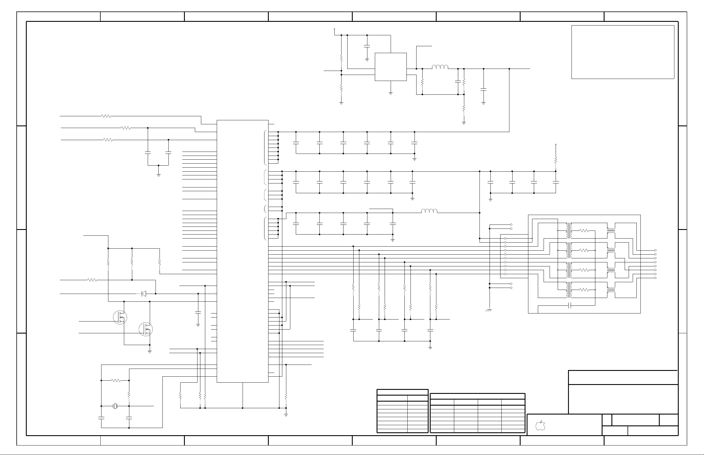
VFB
SW
MODE
RUN
VIN
GND
G
D
S
G
D
S
TX_EN
TXD7
TXD6
TXD5
TXD4
TX_ER
GTX_CLK
125CLK
RX_CLK
TXD0
TXD3
TXD2
TXD1
TX_CLK
VDDOX
VDDOH
VDDO
DVDD
CTRL10
MDC
CRS
COL
RX_ER
RX_DV
RXD7
RXD1
RXD2
RXD3
RXD4
RXD5
RXD6
RXD0
MDI1MDI2+
MDI2MDI3+
MDI1+
MDI0-
MDI0+
AVDD
VSSC
XTAL2
HSDAC-
HSDAC+
S_CLK-
S_CLK+
XTAL1
S_OUT-
S_OUT+
S_IN-
S_IN+
COMA
RESET
INT+
INT-/
MDIO
LED_LINK1000
LED_LINK100
GND
SEL_2.5V
SEL_OSC
TRST
RSET
TDO
TDI
TCK
TMS
CONFIG5
CONFIG6
CONFIG4
CONFIG0
CONFIG1
CONFIG2
CONFIG3
LED_TX
LED_RX
LED_DUPLEX
LED_LINK10
MDI3-
1000PF, 2000VSHIELD
PRIMARY
ENET_CTAP
MDI_2-
MDI_3-
MDI_3+
MDI_1-
MDI_1+
MDI_0-
MDI_0+
MDI_2+
ENET_CTAP
CHIP SIDE
RJ45
75 OHM
1CT:1CT
J3
J2
J1
J5
J6
J7
J8
J4
SECONDARY
CABLE SIDE
RJ45
75 OHM
75 OHM
75 OHM
1CT:1CT
1CT:1CT
1CT:1CT
D
SIZE
OF
SHT
DRAWING NUMBER
NOTICE OF PROPRIETARY PROPERTY
I TO MAINTAIN THE DOCUMENT IN CONFIDENCE
III NOT TO REVEAL OR PUBLISH IN WHOLE OR PART
II NOT TO REPRODUCE OR COPY IT
AGREES TO THE FOLLOWING
PROPERTY OF APPLE COMPUTER, INC. THE POSSESSOR
THE INFORMATION CONTAINED HEREIN IS THE PROPRIETARY
1
2
3
4
5
67
8
12
3
4
5
6
78
B
C
D
A
B
C
D
A
REV.
APPLE COMPUTER INC.
SCALE
NONE
Keep C851 & C852 Stubs short
PLACE ALL SERIES RES CLOSE TO PHY
Y6 LOAD CAPACITANCE IS 16PF
NC
NC
NC
NC
NC
PLACE CAPS (IN ORDER) ON PINS 32/35, 36/40, 45 & 78
PLACE CAPS (IN ORDER) ON PINS 1, 6, 10/15, 57/62, 67/71, 85
PLACE CAPS (IN ORDER) ON PINS 5, 21/26, 48/52, 66/72, 88, 96
PUT CRYSTAL CIRCUIT CLOSE TO PHY
(000)
(BELOW)
SEE CONFIG TABLES
(000)
(101)
(111)
(110)
(111)
(000)
ASLEEP ON BATTERY (SAVES POWER)
PLACES PHY IN "COMA" MODE WHEN
NC
NC
NC
NC
NC
NC
PLACE RESISTORS CLOSE TO PHY
10/100/1000 ETHERNET
PHYADR[0]
PHYADR[3]
75/50 OHM
MODE[3]
MODE[0]
DIS_125
ANEG[1]
BIT[0]BIT[1]
INT_POL
ENA_XC
ANEG[2]
MODE[1]
DIS_SLEEP
PHYADR[4]
PHYADR[1]
CONFIG INPUTS
BIT[2]
DIS_FC
ANEG[3]
ANEG[0]
MODE[2]
ENA_PAUSE
PHYADR[2]
SEL_BDT
CONFIG<3>
CONFIG<6>
CONFIG<5>
CONFIG<4>
CONFIG<0>
CONFIG<1>
CONFIG<2>
PIN
BIT[2:0]
111
000
001
011
010
100
110
101
CONFIG DEFINITIONS
LED_LINK100
LED_LINK1000
PIN
VDDO
VSS
LED_TX
LED_RX
LED_DUPLEX
LED_LINK10
parallel, matched lengths, with minimum
via count, and short if possible
All differential signals should be close,
Must maintain 50-ohms trace impedance on all
Sandwich each RJ54 pair between chassis grounds
2. TX SERIES TERMINATION - LOCATE NEAR LINK
3. RX SERIES TERMINATION - LOCATE NEAR PHY
1. Decoupling caps
MDI pairs and all RJ45 pairs
Ethernet routing priority:
MARVELL 88E1111
R1
VOUT = 0.8V*(1+R2EQV/R1)
R2B
R2A
R2EQV = R2A||R2B
PLACE CAPS AT CONNECTOR PINS 5 & 6
.
49.9
1%
1/16W
MF
402
2
1
R435
1/16W
402
MF
1%
49.9
2
1
R436
MF
1/16W
1%
49.9
402
2
1
R433
402
MF
1/16W
1%
49.9
2
1
R434
402
5%
CERM
50V
27pF
2
1
C604
CERM
50V
5%
402
27pF
2
1
C624
0
402
5%
1/16W
MF
21
R421
402
MF
1/16W
5%
10K
2
1
R430
CHGND1
49.9
1%
MF
402
1/16W
2
1
R439
MF
1/16W
1%
49.9
402
2
1
R437
402
MF
1/16W
49.9
1%
2
1
R440
49.9
1%
1/16W
MF
402
2
1
R438
0.01uF
20%
16V
CERM
402
2
1
C622
402
CERM
16V
20%
0.01uF
2
1
C615
402
CERM
16V
20%
0.01uF
2
1
C617
0.1uF
20%
10V
CERM
402
2
1
C647
0.1uF
402
CERM
10V
20%
2
1
C645
0.1uF
402
CERM
10V
20%
2
1
C648
0.1uF
20%
10V
CERM
402
2
1
C646
NO STUFF
MF
1/16W
1%
49.9
402
2
1
R424
MF
1/16W
1%
49.9
402
NO STUFF
2
1
R429
0
MF
1/16W
5%
402
21
R423
402
MF
1/16W
5%
10K
2
1
R428
MF
0
1/16W
5%
402
21
R445
5%
1/16W
1.5K
MF
402
2
1
R432
4.99K
402
MF
1/16W
1%
2
1
R427
10V
20%
2.2uF
CERM
805
2
1
C611
1K
5%
402
MF
1/16W
21
R422
402
20%
CERM
16V
0.01uF
2
1
C616
0.1uF
CERM
20%
10V
402
2
1
C614
0.01uF
16V
CERM
20%
402
2
1
C602
402
10V
20%
CERM
0.1uF
2
1
C618
10uF
6.3V
20%
805
CERM
2
1
C592
0.1uF
CERM
20%
10V
402
2
1
C598
402
20%
CERM
16V
0.01uF
2
1
C600
0.1uF
CERM
20%
10V
402
2
1
C623
0.01uF
16V
CERM
20%
402
2
1
C612
402
10V
20%
CERM
0.1uF
2
1
C597
10uF
CERM
805
20%
6.3V
2
1
C595
SM
FERR-EMI-600-OHM
12
L35
+2_5V_MAIN
CRITICAL
LTC3405
SOT23-6
4
5
31
6
2
U45
SM1
3.3uH
CRITICAL
21
L60
665K
1/16W
MF
402
1%
2
1
R506
5%
50V
CERM
402
22pF
2
1
C675
49.9K
1%
402
MF
1/16W
2
1
R504
182K
1%
402
MF
1/16W
2
1
R503
NO STUFF
1/16W
MF
0
5%
402
2
1
R513
0.01uF
16V
CERM
20%
402
2
1
C619
402
10V
20%
CERM
0.1uF
2
1
C608
402
20%
CERM
16V
0.01uF
2
1
C601
0.1uF
CERM
20%
10V
402
2
1
C594
402
20%
CERM
16V
0.01uF
2
1
C599
0.1uF
CERM
20%
10V
402
2
1
C603
0
402
5%
MF
1/16W
2
1
R507
1N914
SOT23
3 1
D15
+3V_MAIN
6.3V
805
CERM
20%
10uF
2
1
C674
20%
CERM
805
6.3V
10uF
2
1
C680
2N7002DW
SOT-363
4
5
3
Q32
SOT-363
2N7002DW
1
2
6
Q32
88E1111
BCC
CRITICAL
54
55
53
48
26
72
66
52
96
88
21
5
7
9
4
20
19
18
17
16
14
12
11
47
46
50
44
49
75
77
81
82
80
79
56
13
3
94
2
86
87
89
90
91
93
92
95
30
28
24 43
42
41
39
34
33
31
29
25
68
69
73
74
76
70
23
38
37
8
97
85
71
67
62
57
15
10
6
1
51
84
58
59
60
61
63
64
65
27
83
78
45
40
36
35
32
22
U43
5%
1/16W
MF
402
20K
NO STUFF
21
R425
402
MF
1/16W
5%
0
2
1
R441
402
MF
1/16W
5%
10K
2
1
R431
0.01uF
20%
16V
CERM
402
2
1
C613
603
MF
1/16W
5%
0
2
1
R442
CRITICAL
25.0000M
SM-3
31
Y5
CRITICAL
F-RT-TH
MJ-R0016
9
8
7
6
5
4
3
2
10
1
14
13
12
11
J23
10pF
5%
50V
CERM
402
2
1
C852
NO STUFF
10pF
5%
50V
CERM
402
2
1
C851
26 40
051-6338
C
+2_5V_MARVELL_AVDD
CLKENET_PHY_RX
CLKENET_PHY_GBE_REF
CLKENET_LINK_RX
CLKENET_LINK_GBE_REF
CLKENET_PHY_TX
+2_5V_MARVELL
MDI_M<3>
MDI_P<3>
MDI_M<2>
MDI_P<2>
MDI_M<1>
MDI_P<1>
MDI_M<0>
MDI_P<0>
+2_5V_MARVELL
IO_RESET_L
INT_ENET_RST_L
ENET_RSET
3405_VFB
3405_MODE
MDI3_PDMDI2_PDMDI1_PDMDI0_PD
JTAG_ENET_TDI
SLEEP_L_LS5
AC_IN
JTAG_ASIC_TDO_TP
JTAG_ASIC_TCK
JTAG_ASIC_TMS
JTAG_ASIC_TRST_L
ENET_LINK_RXD<0>
ENET_LINK_RXD<1>
ENET_LINK_RXD<2>
ENET_LINK_RXD<3>
ENET_LINK_RXD<4>
ENET_LINK_RXD<5>
ENET_LINK_RXD<6>
ENET_LINK_RXD<7>
ENET_PHY_TXD<0>
ENET_PHY_TXD<2>
ENET_PHY_TXD<1>
CLKENET_PHY_GTX
ENET_PHY_TX_ER
ENET_PHY_TX_EN
ENET_PHY_TXD<7>
ENET_PHY_TXD<6>
ENET_PHY_TXD<5>
ENET_PHY_TXD<4>
ENET_PHY_TXD<3>
ENET_RX_DV
ENET_COL
ENET_CRS
ENET_RX_ER
ENET_MDC
ENET_MDIO
ENET_ENERGY_DET
ENET_HSDACM
ENET_RST_L
ENET_HSDACP
CLK25M_ENET_XIN
ENET_VSSC
CLK25M_ENET_XOUT
LED_RX_SPN
LED_LINK100
LED_LINK10
CLK25M_XTAL_IN
ENET_COMA
LTC3405_SW
+1_0V_MARVELL
CLKENET_LINK_TX
34 33
29
32
30
35
35
38
39
39
39
39
39
39
39
39
38
23
20
29
39
39
39
37
37
37
37
37
37
37
37
37
37
37
35
37
37
37
37
37
37
37
37
37
37
37
37
37
35
38
35
35
13
13
35
26
37
37
37
37
37
37
37
37
26
17
14
13
18
28
39
13
13
13
13
13
13
13
13
13
13
13
13
13
13
13
13
13
13
13
13
13
13
13
13
13
13
13
13
14
38
38
13
Page 27

OE
GND
OUT
VCC
OSC
SYM_VER2
GND
OUTIN
BYP ADJ
ADJ
BYP
GND
OUT
NC
NC
SHDN
IN
(SYM_VER1)
VREG_PD
PAD
THRML
AGND
SM
TESTM
SE
D5
D6
RESETZ
D7
DGND
PLL
VDD
1.8
3.3
DVDD
PLLGND
PLL
3.3
VDD
D3
D4
D1
D2
BMODE
PC2
PD
PC1
CPS
PC0
D0
LREQ
LPS
LCLK
3.3
AVDD DVDD
1.8
TPA1+
TPA1-
PCLK
TPA0-
TPA0+
TPA2+
TPA2-
C/LKON
CTL0
CTL1
CNA
PINT
TPBIAS0
TPBIAS1
XO
XI
TPBIAS2
R1
R0
TPB2-
TPB2+
TPB1-
TPB1+
TPB0-
TPB0+
DS0
DS1
ON/OFF
GND
VOUT
FB
VIN
PART NUMBER
ALTERNATE FOR
PART NUMBER
BOM OPTION
REF DES
COMMENTS:
TABLE_ALT_HEAD
D
SIZE
OF
SHT
DRAWING NUMBER
NOTICE OF PROPRIETARY PROPERTY
I TO MAINTAIN THE DOCUMENT IN CONFIDENCE
III NOT TO REVEAL OR PUBLISH IN WHOLE OR PART
II NOT TO REPRODUCE OR COPY IT
AGREES TO THE FOLLOWING
PROPERTY OF APPLE COMPUTER, INC. THE POSSESSOR
THE INFORMATION CONTAINED HEREIN IS THE PROPRIETARY
1
2
3
4
5
67
8
12
3
4
5
6
78
B
C
D
A
B
C
D
A
REV.
APPLE COMPUTER INC.
SCALE
NONE
TABLE_ALT_ITEM
SN0201029PFP
1MA (MAX) BUS HOLDERS
0 = Bilingual port
PHY PIN 64
CAPACITOR IN CONJUCTION WITH
DSx Strap Options
1 = A-only port
INTERNAL PULLUP PROVIDES
PHY PIN 25
(DS2)
PHY PINS 4,14
(FW_TPA0P)
RECEIVES POWER
RESET PULSE WHEN PHY FIRST
(MAY PROVIDE POWER, OR
PWR CLASS = 100
MAY REQUIRE UP TO 3W)
(PC0 IS MSB, PC2 IS LSB)
PHY PIN 21
R1
165MA MAX LOAD
VOUT = 1.22*(1+R2/R1)+ IADJ*R2
IADJ = 30NA AT 25C
R2
PHY PIN 40
PHY PIN 50
PHY PIN 61
NC
NC
RX0
PHY PIN 38
NC
NC
(FW_TPB0P)
(FW_TPA0N)
(FW_TPA1P)
(FW_TPA1N)
(FW_TPB0N)
(FW_TPB1P)
(FW_TPB1N)
NC
TX0
PHY PIN 38
PHY PINS 72,76
PHY PIN 28
R2
R1
NC
NC
(FWB-RX)
(FWA-RX)
(FWB-TX)
(FWA-TX)
FIREWIRE PHY
1K
5%
1/16W
MF
402
2
1
R514
6.3V
0.22uF
CERM
20%
402
2
1
C679
22
SM1
1/16W
5%
5
6
7
8
4
3
2
1
RP38
5%
1/16W
SM1
22
5
6
7
8
4
3
2
1
RP37
MF
1/16W
5%
22
402
21
R519
22
5%
402
MF
1/16W
21
R520
0.1uF
402
20%
10V
CERM
2
1
C683
16V
0.01uF
402
CERM
20%
2
1
C610
98.304M
SM-A
CRITICAL
4
3 1
2
G2
402
1/16W
5%
0
MF
2
1
R508
MF
1/16W
5%
100K
402
NO STUFF
2
1
R412
402
MF
1/16W
5%
47
21
R510
402
MF
1/16W
5%
100
2
1
R511
0.22uF
402
6.3V
20%
CERM
2
1
C583
10V
20%
603
CERM
1uF
21
C584
10V
20%
CERM
603
1uF
21
C596
1uF
10V
20%
CERM
603
21
C606
10V
20%
603
CERM
1uF
21
C593
603
1
5%
1/16W
MF
21
R413
1
5%
1/16W
MF
603
21
R420
1/16W
603
MF
5%
1
21
R426
1
5%
1/16W
MF
603
21
R418
SOT-23-1
LTC1761ES5-BYP
CRITICAL
51
2
3 4
U44
2.2uF
20%
10V
CERM
805
2
1
C671
1%
1/16W
MF
402
16.2K
2
1
R496
402
MF
1/16W
1%
27.4K
21
R495
16.2K
1%
1/16W
MF
402
2
1
R443
27.4K
1/16W
1%
MF
402
2
1
R444
805
CERM
10V
20%
2.2uF
2
1
C625
603
MF
1/16W
5%
1
21
R419
10V
20%
603
CERM
1uF
21
C586
10V
20%
CERM
603
1uF
21
C678
603
MF
1/16W
5%
3.3
2
1
R416
3.3
5%
1/16W
MF
603
2
1
R415
2.2uF
20%
10V
CERM
805
2
1
C585
20%
10V
805
CERM
2.2uF
2
1
C588
603
MF
1/16W
5%
10
2
1
R414
400-OHM-EMI
SM-1
2
1
L34
LT1962-ADJ
MSOP
CRITICAL
5
1
7
6
8
4
3
2
U38
0.1uF
402
20%
CERM
10V
2
1
C590
603
MF
1/16W
5%
1
21
R417
0.1uF
402
CERM
10V
20%
21
C591
5%
1K
1/16W
MF
402
2
1
R501
SC-59
SDM20E40C
3
2
1
D25
+5V_SLEEP
1K
402
MF
1/16W
5%
2
1
R505
CRITICAL
PQFP
TSB81BA3A
26
27
73
60
54
47
55
56
48
49
41
42
58
59
52
53
45
46
81
78
36
35
75
22
23
31
30
29
28
25
1
77
5
68
67
66
3
80
7
706918
6
716537
8
32
33
7672643814
4
20
19
17
16
15
13
12
11
2
10
9
34
79
74
6357514439
24
6261504340
21
U36
0.1uF
402
20%
10V
CERM
2
1
C677
10uF
20%
6.3V
CERM
805
2
1
C620
402
1/16W
MF
1%
56.2
2
1
R491
56.2
1/16W
MF
402
1%
2
1
R492
56.2
MF
402
1%
1/16W
2
1
R487
0.1uF
20%
CERM
402
10V
2
1
C676
402
MF
1/16W
1%
56.2
2
1
R488
1uF
CERM
20%
10V
603
2
1
C607
1uF
10V
20%
CERM
603
2
1
C605
402
MF
56.2
1%
1/16W
2
1
R489
1%
MF
402
1/16W
4.99K
2
1
R498
MF
402
56.2
1/16W
1%
2
1
R490
220pF
402
CERM
25V
5%
C672
402
MF
56.2
1%
1/16W
2
1
R493
402
MF
1/16W
1%
4.99K
2
1
R499
1%
1/16W
MF
402
56.2
2
1
R494
220pF
402
CERM
25V
5%
C673
1K
5%
1/16W
402
MF
2
1
R486
20%
0.1uF
CERM
402
10V
2
1
C682
10uF
20%
6.3V
CERM
805
2
1
C681
16V
0.01uF
CERM
20%
402
2
1
C621
10uF
805
CERM
6.3V
20%
2
1
C609
0.1uF
402
CERM
10V
20%
2
1
C587
100uF
20%
10V
POLY
SMD-3
2
1
C670
SM-3
220uH
CRITICAL
21
L59
MBR0540
SM
2
1
D16
CRITICAL
SM
LM2594
8
7
56
4
U37
10uF
50V
CERM
2320
N20P20%
2
1
C665
402
MF
1%
1/16W
402K
2
1
R502
0.1uF
20%
10V
CERM
402
2
1
C589
402
MF
1/16W
5%
22
21
R518
10V
0.1uF
CERM
20%
402
2
1
C684
402
6.34K
1%
1/16W
MF
12
R512
10K
5%
1/16W
MF
402
1
2
R516
1K
402
5%
MF
1/16W
2
1
R497
402
MF
1/16W
5%
1K
2
1
R509
402
5%
1/16W
MF
1K
2
1
R515
402
MF
1/16W
5%
470
2
1
R500
402
MF
1/16W
1K
5%
2
1
R517
C
051-6338
4027
G2197S0011197S0052
Alt. for SunnyEMI Part
FW_TPA1P
+1_95V_FW_DVDD
FW_TPI0N
FW_TPO0P
FW_TPB1N
FW_BIAS1
+1_95V_FW_DVDD_RX0
+1_95V_FW_PLLVDD
+1_95V_FW_DVDD
FW_CORE_ADJ
FW_CORE_BYP
LM2594_IN
FW_PHY_CNTL<1>
+1_95V_FW_DVDD
+1_95V_FW_PLLVDD
CLKFW_LINK_PCLK
FWB_TPB1FWB_TPB0
FW_OSC_EN
FW_OSC
+3V_FW_UF
FW_PLL_ADJ
FWPLL_BYP
FW_LINK_DATA<0>
FW_LINK_DATA<1>
FW_LINK_DATA<2>
FW_LINK_DATA<3>
FW_LINK_DATA<4>
FW_LINK_DATA<5>
FW_LINK_DATA<6>
FW_LINK_DATA<7>
+FW_PWR_OR
+FW_PWR_OR
+3V_FW
FW_LINK_CNTL<0>
CLKFW_PHY_PCLK
FW_LINK_CNTL<1>
FW_PHY_CNTL<0>
+1_95V_FW_DVDD_TX0
FW_VREG_PD
FW_TESTM
FW_PHY_RESET_L
FW_PHY_DATA<7>
FW_PHY_DATA<6>
FW_PHY_DATA<5>
+1_95V_FW_DVDD_PORT1
+3V_FW
+1_95V_FW_PLL500VDD
+1_95V_FW_PLL400VDD
FW_PHY_DATA<3>
FW_PHY_DATA<2>
FW_PHY_DATA<1>
FW_PHY_DATA<4>
FW_BMODE
FW_CPS
FW_PHY_DATA<0>
FW_PC_PD
FW_PHY_PD
FW_PC_PU
FW_PHY_LREQ
FW_PHY_LPS
CLKFW_PHY_LCLK
+3V_FW_AVDD_PORT1
+3V_FW_AVDD_PORT0
+3V_FW_AVDD
+3V_FW_AVDD_PORT2
FW_TPA1N
CLKFW_PHY_PCLK
FW_TPO0N
FW_LKON
FW_PHY_CNTL<1>
FW_PHY_CNTL<0>
FW_PINT
FW_BIAS0
FW_XI
FW_R0
FW_R1
FW_TPB2_PD
FW_TPB1P
FW_TPI0P
FW_INPUT_PD
FW_PORT1_SEL
39
39
38
38
38
38
39
39
37
38
37
37
37
38
38
37
38
38
35
37
37
37
37
37
37
37
37
28
28
28
37
35
37
37
28
37
35
37
35
37
37
37
37
37
37
28
27
28
28
28
38
27
27
38
27
27
27
13
35
38
13
13
13
13
13
13
13
13
27
27
27
13
27
13
27
38
37
37
37
38
27
38
38
37
37
37
37
37
14
13
13
13
38
38
38
38
28
27
28
13
27
27
13
35
28
28
Page 28

SYM_VER-1
SYM_VER-1
G
D
S
SYM_VER-2
SYM_VER-2
VP
VGND
TPI#
TPO
TPI
TPO#
G
D
S
D
SIZE
OF
SHT
DRAWING NUMBER
NOTICE OF PROPRIETARY PROPERTY
I TO MAINTAIN THE DOCUMENT IN CONFIDENCE
III NOT TO REVEAL OR PUBLISH IN WHOLE OR PART
II NOT TO REPRODUCE OR COPY IT
AGREES TO THE FOLLOWING
PROPERTY OF APPLE COMPUTER, INC. THE POSSESSOR
THE INFORMATION CONTAINED HEREIN IS THE PROPRIETARY
1
2
3
4
5
67
8
12
3
4
5
6
78
B
C
D
A
B
C
D
A
REV.
APPLE COMPUTER INC.
SCALE
NONE
PORT POWER SWITCH
INT-SHIELD
INT-SHIELD
TPA
514S0058
(BREF)
TPA*
PER 1394B V1.33
TPB*
(BILINGUAL)
(TPI0R)
AREF NEEDS TO BE ISOLATED FROM
ALL LOCAL GROUNDS PER 1394B SPEC
(TO AVOID GROUND OFFSET ISSUE)
AND CONNECTION DETECTION CURRENTS
LOGIC GROUND FOR SPEED SIGNALING
BREF SHOULD BE HARD CONNECTED TO
THERE’S NO DC PATH BETWEEN THEM
PLUGGED TO A BETA-ONLY DEVICE,
SO WHEN A BILINGUAL DEVICE IS
NC
TPB(R)
VG
VP
TPB
SC
TPA(R)
(AREF)
1394a/b
PORT 0
PORT 1
FIREWIRE PORTS
514-0057
CLEAR OUT ALL PLANES UNDER TRANSFORMERS
1394a ONLY
MACHINE IS RUNNING OR WHEN ASLEEP ON AC
ENABLES PORT POWER WHEN
2
1
R465
MF
1/16W
5%
1M
402
CHGND1
2
1
R448
1/16W
402
5%
MF
470K
2
1
R461
402
MF
5%
1/16W
330K
2
1
C639
402
CERM
20%
0.01UF
16V
2
1
C651
16V
NO STUFF
CERM
402
20%
0.01uF
61
DP6
BAS16TW
SOT-363
21
D24
CRITICAL
B340B
SMB
2
1
R777
402
MF
1/16W
5%
470K
2
1
C650
402
CERM
16V
20%
0.01uF
9
8
7
6
5
4
3
2
15
14
13
12
11
10
1
J20
CRITICAL
F-RT-SM
1394B
4
3 2
1
L76
CRITICAL
90-OHM-300mA
2012H
4
3 2
1
L77
CRITICAL
90-OHM-300mA
2012H
3
2
1
4
8
7
6
5
Q34
SOI
NDS9407
CRITICAL
1
2
R466
805
0
5%
1/10W
FF
1
2
6
Q33
2N7002DW
SOT-363
6
2
1
D18
SOT-363
BAV99DW
3
5
4
D22
BAV99DW
SOT-363
3
5
4
D18
SOT-363
BAV99DW
3
21
4
L52
SM1
260-OHM-330MA
3
21
4
L48
SM1
260-OHM-330MA
6
2
1
D22
BAV99DW
SOT-363
1
2
5
6
3
4
10
987
J24
F-RT-TH
CRITICAL
1394A
2
1
C666
CERM
402
20%
16V
0.01uF
CHGND1
2
1
C662
402
CERM
16V
20%
0.01uF
2
1
C649
0.1uF
20%
50V
805
CERM
2
1
R471
0
5%
1/10W
FF
805
6
2
1
D23
SOT-363
BAV99DW
+3V_PMU
2
1
R447
1/16W
100K
MF
5%
402
4 3
DP6
BAS16TW
SOT-363
3
5
4
D23
BAV99DW
SOT-363
52
DP6
SOT-363
BAS16TW
4
5
3
Q33
2N7002DW
SOT-363
2 1
R446
402
MF
1/16W
5%
10K
CHGND1
2
1
C652
NO STUFF
0.01uF
402
CERM
16V
20%
3
5
4
D20
BAV99DW
SOT-363
2
1
L58
SM
FERR-250-OHM
2
1
L51
FERR-250-OHM
SM
6
2
1
D20
BAV99DW
SOT-363
21
R451
10K
5%
MF
402
1/16W
21
L39
SM-1
400-OHM-EMI
2
1
C630
402
CERM
10V
20%
0.1UF
2
1
C638
0.01UF
20%
CERM
402
16V
3
1
D21
1N5227B
SOT23
2
1
C637
402
CERM
50V
20%
0.001UF
2
1
C640
0.01UF
20%
16V
CERM
402
2
1
F1
1.5AMP-33V
SM
2
1
C633
402
0.01UF
20%
16V
CERM
2
1
C644
0.01UF
20%
16V
CERM
402
21
F3
SM
1.5A-24V
+PBUS
C
051-6338
28 40
FW_GATE_EN_RC
FW_POWER_UP
AC_IN_FW_CNTL
AC_IN
PMU_POWER_UP_L
DCDC_EN
POWER_UP
FW_GATE_EN
+FW_PBUS
+FW_SW
FW_VGND0
+FW_PWR_OR
+3V_FW_ESD_ILIM
+FW_PWR1
+FW_VP1
+3V_FW_ESD
FW_VGND1
FW_TPO1P
FW_TPI1P
FW_TPI1N
FW_TPO1N
FW_TPA1N
FW_TPA1P
+3V_FW
FW_TPB1N
+FW_VP0
FW_TPAO0P
FW_TPAO0N
FW_TPO0P
FW_TPBI0P
FW_TPBI0N
FW_TPI0N
FW_TPB1P
FW_TPO0N
+3V_FW_ESD
FW_TPO0R
FW_TPI0P
26
20
27
27
27
27
29
29
32
27
38
37
37
37
37
27
27
27
27
38
37
37
27
37
37
30
32
33
38
38
38
38
38
39
28
38
39
39
39
39
37
37
38
37
39
37
37
39
37
37
39
37
39
28
39
39
Page 29
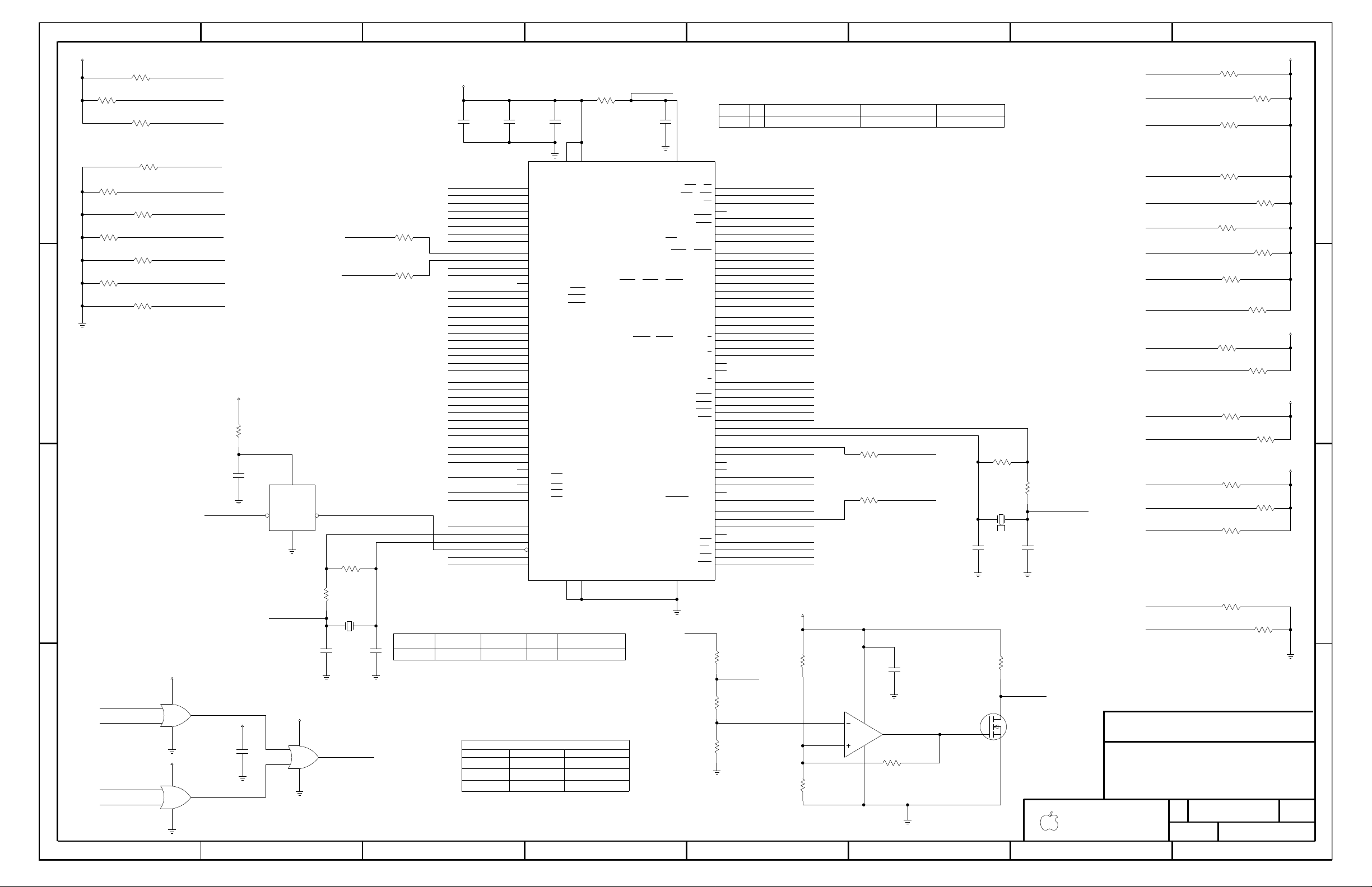
S
D
G
A
B
Y
A
B
Y
A
B
Y
P86_XCOUT
AVSS
VSS
XIN
RESET
VREF
CNVSS
BYTE
XOUT
AVCC
P50_WRL_WR
P51_WRH_BHE
P52_RD
P65_CLK1
P66_RXD1
P67_TXD1
P74_TA2OUT_W
P75_TA2IN_W
P60_CTS0_RTS0
P57_RDY_CLKOUT
P56_ALE
P55_HOLD
P54_HLDA
P53_BCLK
P61_CLK0
P62_RXD0
P63_TXD0
P70_TXD2_SDA_TA0OUT
P72_CLK2_TA1OUT_V
P73_CTS2_RTS2_TA1IN_V
P100_AN0
P90_TB0IN_CLK3
P91_TB1IN_SIN3
P92_TB2IN_SOUT3
P93_DA0_TB3IN
P94_DA1_TB4IN
P95_ANEX0_CLK4
P96_ANEX1_SOUT4
P97_ADTRG_SIN4
P87_XCIN
P85_NMI
P84_INT2
P83_INT1
P82_INT0
P81_TA4IN_U
P80_TA4OUT_U
P77_TA3IN
P76_TA3OUT
P107_AN7_KI3
P106_AN6_KI2
P105_AN5_KI1
P104_AN4_KI0
P103_AN3
P102_AN2
P101_AN1
P64_CTS1_RTS1_CTS0_CLKS1
P71_RXD2_SCL_TA0IN_TB5IN
VCC
P01_D1
P00_D0
P02_D2
P03_D3
P04_D4
P05_D5
P06_D6
P07_D7
P10_D8
P11_D9
P12_D10
P13_D11
P21_A1_D1_D0
P22_A2_D2_D1
P23_A3_D3_D2
P24_A4_D4_D3
P25_A5_D5_D4
P14_D12
P17_D15_INT5
P15_D13_INT3
P16_D14_INT4
P20_A0_D0
P27_A7_D7_D6
P26_A6_D6_D5
P30_A8_D7
P31_A9
P32_A10
P33_A11
P34_A12
P35_A13
P36_A14
P37_A15
P45_CS1
P46_CS2
P47_CS3
P44_CS0
P43_A19
P40_A16
P41_A17
P42_A18
RSET*
MR*
GND
VCC
PART NUMBER
ALTERNATE FOR
PART NUMBER
BOM OPTION
REF DES
COMMENTS:
TABLE_ALT_HEAD
REFERENCE DESIGNATOR(S)
BOM OPTION
TABLE_5_HEAD
QTY
DESCRIPTION
PART#
D
SIZE
OF
SHT
DRAWING NUMBER
NOTICE OF PROPRIETARY PROPERTY
I TO MAINTAIN THE DOCUMENT IN CONFIDENCE
III NOT TO REVEAL OR PUBLISH IN WHOLE OR PART
II NOT TO REPRODUCE OR COPY IT
AGREES TO THE FOLLOWING
PROPERTY OF APPLE COMPUTER, INC. THE POSSESSOR
THE INFORMATION CONTAINED HEREIN IS THE PROPRIETARY
1
2
3
4
5
67
8
12
3
4
5
6
78
B
C
D
A
B
C
D
A
REV.
APPLE COMPUTER INC.
SCALE
NONE
TABLE_5_ITEM
TABLE_ALT_ITEM
ID RANGE
2.31-2.97V
0.33-0.99V
will act as our pulldown since
to +3V_MAIN or +3V_SLEEP, which
(PMU_AP)
.
KEEP CAP CLOSE TO ALL 3 OR GATES
PMU KEYBOARD RESET CIRCUIT
AIRLINE
Q11 (65W)
ADAPTER IDs
ADAPTER
A29 (45W)
1.65-2.31V
PIN VOLTAGE
2.558-2.661V
2.007-2.066V
0.589-0.663V
PMU
reset. MLB will have a pull-up
have a pulldown for coming out of
NC
(CHARGE_I)
NC
NC
NC
NC
NC
NC
NC
NC
UNDERVOLTAGE RESET CIRCUIT
Y3’S LOAD CAPACITANCE IS 12.5PF
Keep crystal subcircuit close to PMU.
A29 ADAPTER DETECTION
both are off during PMU reset.
Keep crystal subcircuit close to PMU.
Y5’S LOAD CAPACITANCE IS 12PF
CPU_VCORE_HI_OC/PMU_AP should
+3V_PMU
+3V_SLEEP
+3V_PMU
2
1
3
Q30
SM
2N7002
4
5
3
2
1
U20
SC70
NC7S32
4
5
3
2
1
U24
NC7S32
SC70
4
5
3
2
1
U25
NC7S32
SC70
2
1
C277
0.1uF
20%
10V
402
CERM
+3V_PMU
21
Y4
10.0000M
CRITICAL
8X4.5MM-SM
+5V_SLEEP
12
R564
1/16W
MF
5%
10K
402
+3V_MAIN
12
R575
10K
1/16W
MF
5%
402
12
R599
402
5%
MF
1/16W
10K
12
R598
10K
1/16W
MF
5%
402
12
R563
1/16W
MF
5%
10K
402
12
R576
402
100K
5%
MF
1/16W
12
R562
1/16W
MF
402
100K
5%
21
R561
100K
1/16W
MF
5%
402
21
R594
402
10K
1/16W
MF
5%
2
1
C731
CERM
20%
10V
402
0.1uF
11
13
6212
96
6014
10
98
99
100
1
2
3
4
5
8
9
15
16
17
18
19
20
21
22
23
24
25
26
27
28
29
30
31
32
33
34
35
36
37
38
39
40
41
42
43
44
45
46
47
48
49
50
51
52
53
54
55
56
57
58
59
61
63
64
65
66
67
68
69
70
71
72
73
74
75
76
77
78
87
88
89
90
91
92
93
95
79
80
81
82
83
84
85
86
7
6
94
97
U29
OMIT
M16C62
FLAS
21
R602
1/16W
MF
402
4.7
5%
12
R589
1/16W
MF
402
470K
5%
2
1
C724
0.1uF
CERM
20%
10V
402
2
1
C729
402
10V
20%
CERM
0.1uF
2
1
R249
402
MF
1/16W
5%
0
21
R248
NO STUFF
1/16W
MF
402
5%
10M
2
1
C340
CERM
50V
5%
402
12pF
2
1
C339
402
50V
5%
12pF
CERM
21
R588
402
1K
MF
1/16W
5%
21
R600
1/16W
MF
402
1K
5%
+3V_PMU
+3V_PMU
12
R261
100K
402
5%
MF
1/16W
+3V_PMU
+3V_PMU
2
1
C255
805
20%
CERM
10uF
6.3V
21
R597
5%
1/16W
MF
2.2K
402
21
R595
470K
MF
1/16W
5%
402
+3V_PMU
21
R582
402
5%
1/16W
MF
10K
21
R560
402
5%
1/16W
MF
100K
1
2
R592
402
MF
1/16W
1%
100K
21
R583
10K
402
5%
1/16W
MF
63
RP39
SM1
5%
1/16W
100K
54
RP39
SM1
100K
1/16W
5%
81
RP39
SM1
5%
1/16W
100K
21
R596
402
MF
1/16W
5%
2.2K
+3V_PMU
4
23
1
U26
MAX6804
SOT143
2
1
R267
5%
402
MF
1/16W
1K
2
1
C370
0.1uF
20%
10V
402
CERM
12
R591
402
MF
1/16W
470K
5%
21
R580
5%
1/16W
NO STUFF
10M
MF
402
2
1
C728
12pF
402
5%
CERM
50V
2
1
R581
5%
402
MF
1/16W
0
2
1
C406
402
CERM
50V
12pF
5%
12
R586
MF
1/16W
5%
402
10K
72
RP39
SM1
5%
1/16W
100K
72
RP41
1/16W
5%
10K
SM1
12
R587
1K
402
5%
1/16W
MF
2
1
R593
100K
1%
1/16W
MF
402
2
1
R590
402K
1%
1/16W
MF
402
31
42
Y3
CRITICAL
32.768K
SM-2
12
R584
402
MF
1/16W
7.15K
1%
12
R585
1/16W
MF
402
7.15K
1%
54
RP41
SM1
10K
5%
1/16W
81
RP41
10K
5%
1/16W
SM1
63
RP41
SM1
10K
5%
1/16W
2
5
1
3
4
U33
LMC7211
SM
2
1
R348
1%
1/16W
MF
402
52.3K
2
1
R349
1%
402
MF
1/16W
127K
21
R345
1/16W
MF
402
4.7M
5%
2
1
R364
5%
1/16W
MF
402
100K
2
1
C467
CERM
402
0.1uF
20%
10V
C
40
29
051-6338
IC,PMU,V81B
U29
341S1008
1
Y4
197S0604 197S0041
Alt. for Siward Part
+3V_PMU_AVCC
CPU_VCORE_HI_OC
KBD_Y<5>
CLK10M_PMU_XIN
CLK10M_PMU_XOUT_UF
INT_SUSPEND_ACK_L
SYSTEM_CLK_EN
PMU_FROM_INT
CLK32K_PMU_XIN
CLK32K_PMU_XOUT_UF
PMU_OOPS
INT_PEND_PROC_INT
KBD_Y<3>
KBD_X<5>
KBD_COMMAND_L
PMU_PME_L
POWER_VALID
TPAD_RXD
PMU_BATT_DET_L
PMU_SLEEP_LED_L
PMU_LID_CLOSED_L
POWER_VALID
PMU_NMI_L
THERM_L_OC
CLK32K_PMU_XOUT
PMU_BATT1_DET_L_PU
PMU_AC_IN
PMU_AC_DET
PMU_BYTE
PMU_CNVSS
INT_SUSPEND_REQ_L
+3V_PMU_RESET
PMU_KB_RESET_L
CAPSLOCK_LED_L
PMU_CAPSLOCK_LED_L
INT_RESET_L
IO_RESET_L
SLEEP
MAIN_RESET_L
PMU_POWER_UP_L
SOFT_PWR_ON_L
CHARGE_LED_L
NUMLOCK_LED_L
PMU_NUMLOCK_LED_L
AC_IN
PMU_BATT0_DET_L
+3V_PMU_AVCC
PMU_CNVSS
PMU_BYTE
PMU_INT_NMI
INT_PU_RESET_L
PMU_CPU_HRESET_L
PMU_TO_INT
PMU_ACK_L
PMU_CLK
PMU_REQ_L
PMU_RESET_BUTTON_L
PMU_NMI_BUTTON_L
TPAD_RXD
TPAD_TXD
CPU_CLK_EN
PMU_CHARGE_V
PMU_CHRG_BATT_0
CPU_SMI_L
INT_PROC_SLEEP_REQ_L
PMU_POWERUP_OK
PMU_I2C_CLK
PMU_I2C_DATA
PMU_SMB_CLK
PMU_SMB_DATA
KBD_Y<1>
KBD_Y<0>
KBD_Y<2>
KBD_Y<4>
KBD_Y<7>
KBD_Y<6>
PMU_POWER_UP_L
CHARGE_LED_L
COMM_RING_DET_L
SOFT_PWR_ON_L
KBD_X<0>
INT_WATCHDOG_L
KBD_X<2>
KBD_X<1>
KBD_X<4>
KBD_X<3>
KBD_X<7>
KBD_X<6>
KBD_X<9>
KBD_X<8>
IO_RESET_L
KBD_CONTROL_L
KBD_FUNCTION_L
KBD_OPTION_L
KBD_SHIFT_L
KBD_ID
PMU_INT_L
CPU_PLL_STOP_OC
SLEEP
INT_SUSPEND_REQ_L
PMU_OOPS
INT_PU_RESET_L
PMU_LID_CLOSED_L
PMU_I2C_DATA
PMU_I2C_CLK
PMU_PME_L
TPAD_TXD
PMU_NMI_L
PMU_NMI_BUTTON_L
PMU_BATT1_DET_L_PU
PMU_POWERUP_OK
PMU_BATT_DET_L
PMU_EPM
PMU_RESET_BUTTON_L
PMU_SMB_DATA
PMU_SMB_CLK
PMU_KB_RESET_L
PMU_KB_RESET_IN1
SOFT_PWR_ON_L
KBD_CONTROL_L
PMU_KB_RESET_IN2
KBD_SHIFT_L
KBD_OPTION_L
+4_85V_RAW
ADAPTER_DET
PMU_AC_DET
A29_DET_REF
A29_DET_L
A29_DETECT
INT_RESET_L
MAIN_RESET_L
PMU_EPM
CLK10M_PMU_XOUT
PMU_RESET_L
39
39
39
29
39
29
39
34
24
39
39
34
39
39
24
29
29
32
19
33
33
29
32
29
33
19
38
24
39
29
29
26
29
18
32
29
39
30
38
29
32
39
39
29
26
39
39
39
29
29
39
24
39
29
39
39
39
29
18
29
33
39
39
39
39 17
29
30
23
29
39
39
13
23
25
17
29
23
29
28
29
25
39
29
29
29
30
30
39
39
39
39
39
39
29
29
25
23
39
39
39
39
39
39
39
39
39
23
29
39
29
29
39
25
29
25
29
17
29
30
29
30
30
39
23
29
29
29
38
39
13
17
25
7
23
8
14
14
29
14
23
23
23 14
29
23
29
23
39
29
29
25
29
29
29
29
8
33
29
23
9
17
23
14
28
22
25
23
26
25
29
29
14
13
6
14
14
14
14
23
29
23
23
8
30
30
5
14
29
29
29
29
29
23
23
23
23
23
23
28
25
14
22
23
14
23
23
23
23
23
23
23
23
17
23
23
23
23
23
14
7
23
8
29
13
23
29
29
14
23
29
29
29
29
29
29
23
29
29
29
22
23
23
23
31
25
29
30
9
14
29
Page 30
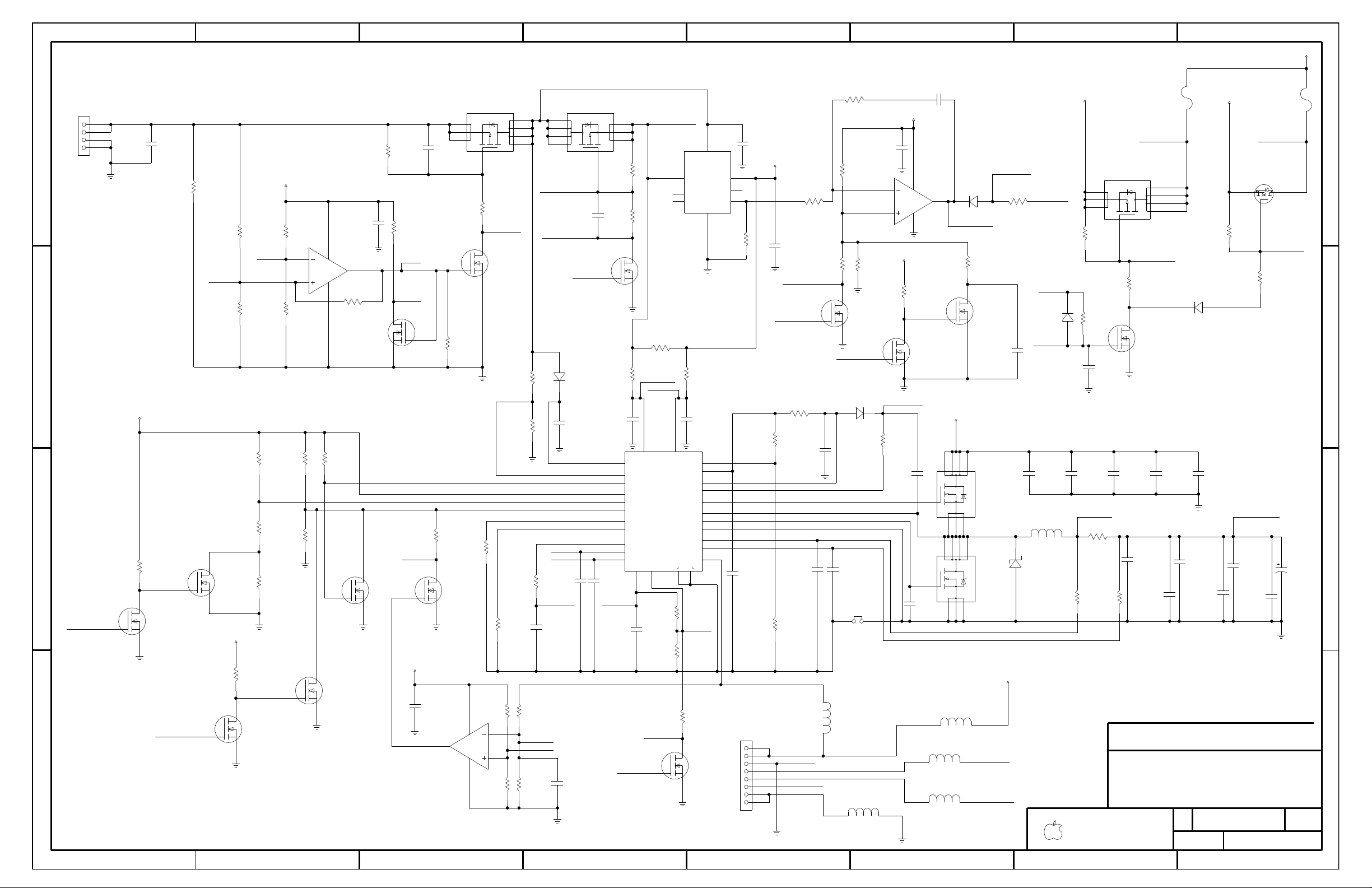
CSIP
CSIN
BATT
PGND
DLO
LX
DHI
BST
DLOV
LDO
CELLS
GND
CSSNCSSP
REF
CCS
CCI
CCV
IINP
ICHG
ICTL
VCTL
RFIN
ACOK
ACIN
DCIN
CLS
S2
GATE
S1
S3 D4
D3
D2
D1
S2
GATE
S1
S3 D4
D3
D2
D1
S2
GATE
S1
S3D4
D3
D2
D1
G
D
S
G
D
S
G
D
S
G
D
S
G
D
S
G
D
S
G
D
S
G
D
S
G
D
S
G
D
S
GND
OUT
PG
RS-
V+
RS+
NC2
NC1
G
D
S
G
D
S
G
D
S
G
D
S
S
D
G
D
SIZE
OF
SHT
DRAWING NUMBER
NOTICE OF PROPRIETARY PROPERTY
I TO MAINTAIN THE DOCUMENT IN CONFIDENCE
III NOT TO REVEAL OR PUBLISH IN WHOLE OR PART
II NOT TO REPRODUCE OR COPY IT
AGREES TO THE FOLLOWING
PROPERTY OF APPLE COMPUTER, INC. THE POSSESSOR
THE INFORMATION CONTAINED HEREIN IS THE PROPRIETARY
1
2
3
4
5
67
8
12
3
4
5
6
78
B
C
D
A
B
C
D
A
REV.
APPLE COMPUTER INC.
SCALE
NONE
(GND)
Place close to RS-
PROTECTION
DC INRUSH LIMITER
PLACE R383 CLOSE TO LTC1625
GREATER THAN 13.1V DETECT
DC POWER INPUT
(POWER JACK, ETC. ON SEPARATE BOARD)
BATTERY
CONNECTOR
(BATT_IN_PD)
+PBUS CURRENT LIMIT
PLACE U24 NEXT TO R382
NC
NC
NC
_62
REFIN
ICTL
For 4.20V cells, VCTL = 0.245 REFIN
For 4.15V cells, VCTL = 0.123 REFIN
CHG
BATT
V = CELLS X (4.096 + (0.4096 * V / V ))
I = (0.2048/R ) * (V / V )
VCTL
REFIN
BATTERY CHARGER
(+3V_PMU)
CHARGE DISABLED BY PMU OR INPUT VOLTAGE <18V
SWITCHER VOLTAGE CONTROL SWITCHER CURRENT CONTROL
CHARGE THROTTLED BY LOW BATTERY VOLTAGE
OD OUTPUT LOW - WHEN AC GREATER THAN 18V
BACKFEED
WHEN AC IS IN, P-CHANNEL FETS ARE QUICKLY (DIODE) TURNED OFF
ROUTE LTC1625_ITH CAREFULLY
WHEN AC IS NOT PLUGGED, P-CHANNEL FETS ARE ON
RC TIME IS 480K*10UF @ +3V_PMU
BATTERY SWITCH-OVER CIRCUIT
PMU SELECTS BETWEEN TWO VOLTAGES
15
13
4
20
23
2
28
14
10
98
22
21
24
1
27 26
19
18
3
16
7
5
6
25
17
12
11
U6
CRITICAL
MAX1772
QSOP
2
1
C41
CERM
10V
20%
1uF
603
2
1
R716
1/16W
MF
402
47K
5%
2
1
R717
10K
402
MF
1/16W
5%
3
2
1
4
8
7
6
5
Q6
CRITICAL
SI4435DY
SOI
2
1
F5
SM-2
5AMP-125V
2
1
F4
5AMP-125V
SM-2
2
1
R83
402
MF
1/16W
1%
1K
2
1
R56
1K
1%
1/16W
MF
402
+24V_PBUS
21
R725
FF
33
5%
1/8W
1206
+BATT
+3V_PMU
2
1
C36
50V
20%
0.01uF
CERM
603
3
2
1
4
8
7
6
5
Q68
SI4435DY
SOI
1
2
R29
470K
1/16W
MF
402
5%
2
1
R52
100K
5%
MF
402
1/16W
2
1
C11
0.1uF
805
CERM
50V
20%
1
2
R21
5%
330K
1/16W
MF
402
2
1
C801
CERM
20%
0.01uF
16V
402
21
R41
402
1M
5%
1/16W
MF
+3V_PMU
1
2
R51
1/16W
20K
402
1%
MF
2
1
R16
100K
MF
1/16W
402
1%
1
2
R40
97.6K
402
1%
1/16W
MF
1
2
R30
402
57.6K
MF
1/16W
1%
1
2
R42
10K
1%
1/16W
MF
402
3
2
1
4
8
7
6
5
Q69
SOI
SI4435DY
4
5
3
Q9
SOT-363
2N7002DW
2
1
R102
1%
158K
MF
1/16W
402
31
D6
SOT23
1N914
2
1
R710
402
MF
1/16W
47K
5%
2
1
R711
5%
402
10K
MF
1/16W
2
1
C112
50V
1812
CERM
20%
2.2uF
2
1
C117
2.2uF
1812
50V
CERM
20%
2
1
C113
2.2uF
1812
50V
20%
CERM
2
1
C115
2.2uF
1812
50V
20%
CERM
2
1
C116
2.2uF
1812
50V
20%
CERM
2
1
R720
5%
1/16W
MF
603
1
1
2
6
Q4
SOT-363
2N7002DW
4
5
3
Q4
2N7002DW
SOT-363
2
1
C97
CERM
603
25V
0.1uF
20%
2
1
R59
402
MF
1/16W
100K
5%
2
1
C118
10uF
20%
805
CERM
6.3V
1
2
6
Q71
2N7002DW
SOT-363
2
1
R15
5%
10K
1/16W
MF
402
1
2
R22
5%
402
MF
1/16W
470K
4
5
3
Q1
2N7002DW
SOT-363
1
2
6
Q1
SOT-363
2N7002DW
1
2
6
Q9
2N7002DW
SOT-363
2
1
R58
402
MF
1/16W
1%
10K
4
5
3
Q71
SOT-363
2N7002DW
1
2
6
Q72
SOT-363
2N7002DW
2
1
R741
402
MF
1/16W
100K
5%
4
5
3
Q72
SOT-363
2N7002DW
+3V_PMU
2
1
C96
CERM
50V
805
20%
0.1uF
2
1
R77
2.21K
1/16W
MF
0.1%
603
CRITICAL
2 1
R119
402
MF
150
1%
1/16W
2
5
1
3
4
U1
LMC7211
SM
5 2
DP1
SOT-363
BAS16TW
43
DP1
SOT-363
BAS16TW
2
1
C780
1206
CERM
25V
20%
4.7uF
2
1
R94
100K
402
MF
1/16W
5%
2
1
C777
1206
20%
25V
CERM
4.7uF
2
1
C792
1206
CERM
25V
20%
4.7uF
2
1
C795
1206
20%
25V
CERM
4.7uF
2
1
R53
1%
1/16W
MF
402
4.12K
2
1
R54
MF
402
1/16W
1%
10K
+BATT
21
L6
SM
FERR-50-OHM
21
L4
SM
FERR-EMI-100-OHM
21
L3
SM
FERR-EMI-100-OHM
21
L2
SM
FERR-50-OHM
1
2
L5
FERR-EMI-100-OHM
SM
21
R61
1%
1W
MF
2512
0.025
CRITICAL
+PBUS
8
7
6
5
4
3
2
1
J26
87438-0833
CRITICAL
M-RT-SM
4
3
2
1
J27
87438-0433
M-RT-SM
CRITICAL
321
4
8765
Q64
SO-8
IRF7811W
CRITICAL
+24V_PBUS
2
1
C803
402
CERM
10V
20%
0.1uF
8
21
7
64
3
5
U3
TSSOP
MAX4172
CRITICAL
+24V_PBUS
2
1
R82
4.7
402
MF
1/16W
5%
2
5
1
3
4
U55
SOT23-5
LMC7111
1
2
6
Q74
2N7002DW
SOT-363
4
5
3
Q74
SOT-363
2N7002DW
2
1
C794
0.1uF
20%
10V
CERM
402
2
1
R744
MF
100K
402
1/16W
5%
2
1
R87
4.7
402
MF
1/16W
5%
+3V_PMU
2 1
R727
10K
1%
1/16W
MF
402
2
1
R745
CRITICAL
1/16W
603
FF
42.2K
0.1%
2 1
R728
1K
1%
402
1/16W
MF
21
C798
0.1uF
402
CERM
10V
20%
6 1
DP1
SOT-363
BAS16TW
2
1
C809
20%
10V
CERM
603
1uF
2
1
C71
0.47uF
50V
CERM
20%
1206
2
1
R736
CRITICAL
1/16W
603
0.1%
FF
42.2K
2
1
R742
FF
0.1%
603
1/16W
51.1K
CRITICAL
2
1
R738
603
0.1%
FF
CRITICAL
1/16W
82.5K
2
1
R47
402
MF
1/16W
1%
6.34K
2
1
C35
50V
0.1uF
10%
X7R
603
2
1
D36
SM
MBRS140T3
2
1
C95
0.47uF
CERM
50V
20%
1206
2
1
C826
CERM
50V
0.01uF
20%
603
1
2
6
Q2
2N7002DW
SOT-363
4
5
3
Q2
SOT-363
2N7002DW
3
1
4
Q7
CRITICAL
TO-252
SUD45P03
2
1
C853
NO STUFF
402
X7R
25V
10%
1000pF
2
1
C23
20%
10V
CERM
1uF
603
2
1
R57
1%
1/16W
MF
402
100K
2
1
R49
12.7K
1%
1/16W
MF
402
2
1
C67
1210
CERM
50V
20%
1uF
21
L70
CRITICAL
10uH
SM1
21
R715
2512
MF
1W
1%
0.05
2
1
R713
1
603
MF
1/16W
5%
2
1
C42
0.01uF
20%
16V
CERM
402
2
1
C98
25V
CERM
20%
603
0.1uF
2
1
C99
603
CERM
25V
20%
0.1uF
+3V_PMU
2
1
R73
1%
1/16W
MF
402
27.4K
2
1
R74
MF
4.12K
1%
1/16W
402
2
1
R62
402
MF
1/16W
1%
10K
2
1
R733
1%
1/16W
MF
402
20K
2
1
R75
5.23K
402
MF
1/16W
1%
2
1
C43
20%
16V
CERM
402
0.01uF
2
1
R731
1K
402
MF
1/16W
1%
321
4
8765
Q70
IRF7805
SM
CRITICAL
2
5
1
3
4
U57
SM
LMC7211
+3V_PMU
2
1
R55
402
MF
1/16W
1%
1K
2
1
R729
1/16W
MF
100K
1%
402
2
1
R730
MF
1/16W
100K
1%
402
2
1
R740
1/16W
MF
402
1%
499K
2
1
R735
MF
1/16W
402
1%
100K
2
1
C807
0.047uF
10%
16V
CERM
402
2
1
C799
20%
CERM
0.1uF
10V
402
3
1
D4
1N914
SOT23
2
1
C24
20%
10V
CERM
402
0.1uF
2
1
C790
1206
CERM
25V
20%
4.7uF
2
1
C785
1206
CERM
25V
20%
4.7uF
2
1
C779
33uF
20%
SM1
25V
ELEC
21
XW1
SM
2
1
R96
603
5%
MF
1/16W
4.7
2
1
R732
47K
402
5%
1/16W
MF
2
1
R734
402
1/16W
68K
5%
MF
C
40
30
051-6338
1772_ICTL
+BATT_14V_FUSE
BATT_14V_GATE
1V65_REF
AC_DIV
BATT_LOW
1772_REF
BATT_DIV
+BATT_RSNS
PMU_CHARGE_V
BATTV_LOW
BATTV_HIGH
PMU_CHRG_BATT_0
CHARGE_DISABLE
BATT_LOW_L
1772_ICHG
AC_IN_L
1772_CCV_RC
1772_CCV
1772_IINP
1772_LDO
1772_CCS
1772_CSSP
1772_CSSN
1772_CCI
PMU_SMB_CLK
PMU_SMB_DATA
BATT_24PBUS_EN
AC_ENABLE_L
AC_IN
AC_IN_L_RC
AC_IN_L
AC_GTR_18V
1772_ACOK_L
IAC_FB
IAC_RC_COMP
BATT_CLK
PMU_BATT_DET_L
BATT_NEG
1772_CLS
BATT_14PBUS_EN
+BATT_POS
BATT_DATA
A29_DETECT
A29_DETECT
A29_CLS_ADJ
+BATT_24V_FUSE
AC_IN
1V20_REF
A29_CURRENT_ADJ
1625_COMP
LTC1625_ITH
ADAPTER_I_REG
1772_VCTL
1772_BST_ESR
1772_DCIN
BATT_24V_GATE
+ADAPTER
OVER_18V_ADJ
+BATT_24V_FUSE
+BATT_VSNS
1772_BST
1772_DLOV
CURRENT_THRESHOLD
1772_DHI
1772_LX
MAX4172_OUT
+ADAPTER_SW
1772_ACIN
1772_ACOK_L
+ADAPTER_SENSE
AC_ENABLE_GATE
BKFD_PROT_EN_L
BKFD_PROT_GATE
1772_DLO
1772_GND
1772_CELLS
1772_CSIN
1772_CSIP
30
30
29
29
39
28
39
39
39
30
30
38
28
38
38
38 38
38
29
29
30
38
37
37
29
29
26
30
30
39
29
38
38
39
29
29
30
26
31
31
38
31
30
38
38
38
38
30
38
38
37
37
Page 31
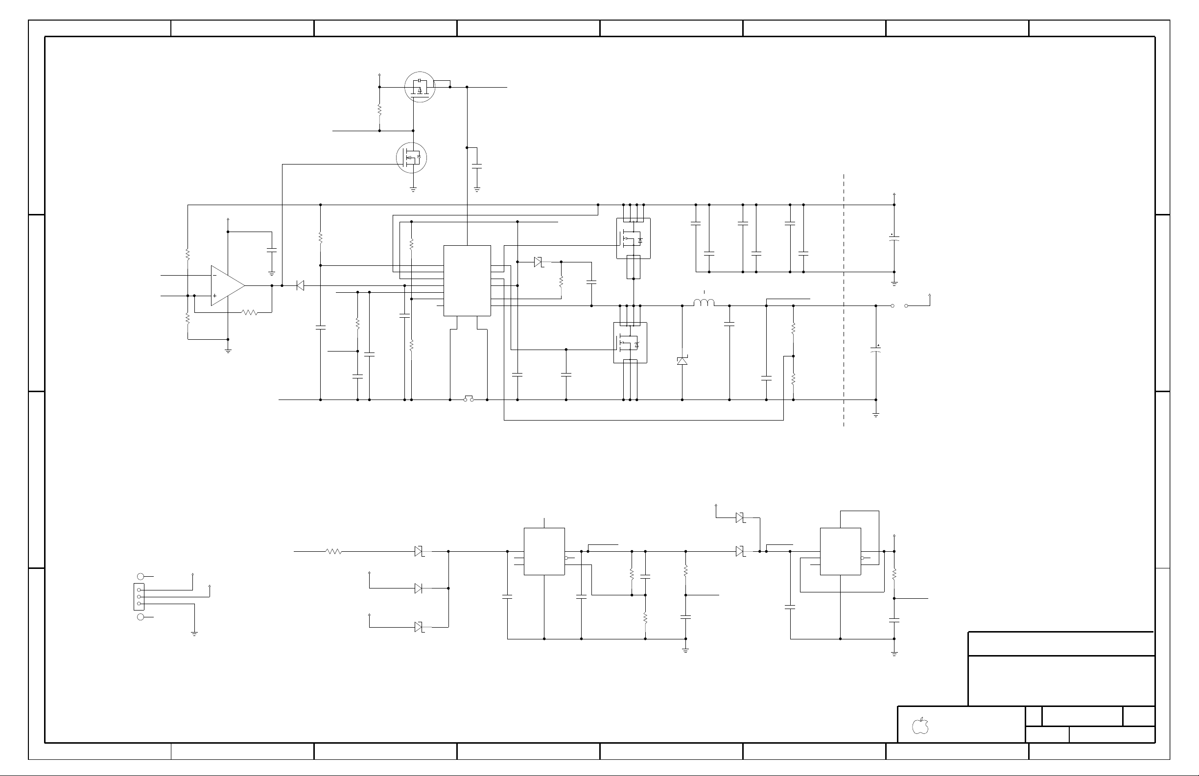
G1
S1
D1
G2
D2
S2
JUMPER
VTAP
IN OUT
SENSE
GND
FDBK
ERR
LP2951
SHUT
SHUT
PLUS5VTAP
LP2951
ERR
FDBK
GND
SENSE
OUTIN
BOOST
SW
SGND PGND
TK
VIN
SYNC
RUN/SS
VPROG
ITH
FCB
INTVCC
TG
VOSENSE
BG
LTC1625
EXTVCC
D
SIZE
OF
SHT
DRAWING NUMBER
NOTICE OF PROPRIETARY PROPERTY
I TO MAINTAIN THE DOCUMENT IN CONFIDENCE
III NOT TO REVEAL OR PUBLISH IN WHOLE OR PART
II NOT TO REPRODUCE OR COPY IT
AGREES TO THE FOLLOWING
PROPERTY OF APPLE COMPUTER, INC. THE POSSESSOR
THE INFORMATION CONTAINED HEREIN IS THE PROPRIETARY
1
2
3
4
5
67
8
12
3
4
5
6
78
B
C
D
A
B
C
D
A
REV.
APPLE COMPUTER INC.
SCALE
NONE
12.8V PBUS SUPPLY
NC
12.8V REGULATOR
NC
PMU SUPPLY
3V_PMU_SENSE
WHEN +24V_PBUS IS BELOW ~13.1V,
1625 IS SHUT-OFF
KEEP VIN/TK LOOP SHORT
CONNECT LTC1625 TK PIN AT TOP-SIDE FET
PBUS HOLD-UP CAPS
ADAPTER OR BATTERY
BATTERY
BOOTSTRAP SYSTEM FROM
BACKUP
OUTPUT FROM BATTERY
INPUT TO AND OUTPUT
FROM BATTERY
1
2
R127
603
MF
1/16W
5%
1
+PBUS
1
2
R107
402
1%
1/16W
MF
4.99K
321
4
8765
Q17
CRITICAL
IRF7805
SM
+24V_PBUS
3 1
D8
1N914
SOT23
2
1
C804
20%
ELEC
35V
100uF
SM-1
2
1
C806
25V
20%
ELEC
SM
220uF
2
1
C134
0.1uF
402
CERM
10V
20%
2
1
R108
402
MF
1/16W
1%
158K
2
1
R109
1%
1/16W
MF
402
16.2K
2
5
1
3
4
U14
LMC7211
SM
+3V_PMU
2
1
C772
0.1uF
20%
CERM
402
10V
2
1
R690
1/16W
MF
402
1%
97.6K
2
1
R673
402
1%
10K
MF
1/16W
21
R663
1/16W
MF
1%
402
1M
1
5
6
Q15
FDG6324L
SC70-6
CRITICAL
4
3
2
6
Q15
SC70-6
CRITICAL
FDG6324L
+5V_MAIN
2
1
R130
5%
402
1/16W
470K
MF
21
XW26
OPEN
2
1
R122
603
MF
1/16W
5%
2.2
2
1
C119
4.7uF
20%
CERM
10V
1206
2
1
R120
402
MF
1/16W
5%
0
NO STUFF
2
1
R118
402
MF
1/16W
5%
0
21
XW3
SM
OMIT
21
D1
SM
MBR0540
21
R39
390
5%
1/4W
FF
1210
+BATT
+PBUS
21
D2
SM
MBR0540
+3V_PMU
2
1
R231
MF
5%
1
1/16W
603
2
1
C326
10uF
6.3V
20%
805
CERM
2
1
C753
2.2uF
20%
1812
CERM
50V
6
3
2
18
4
7
5
U22
SOI-3.3V
21
D10
SM
MBR0520LT
21
D11
SM
MBR0520LT
2
1
C740
0.1uF
10V
402
20%
CERM
+5V_MAIN
2
1
R233
MF
5%
1
1/16W
603
2
1
C336
2.2uF
20%
CERM
10V
805
2
1
C276
603
50V
470pF
10%
CERM
2
1
C155
2.2uF
20%
1812
CERM
50V
2
1
R604
294K
402
1%
MF
1/16W
2
1
R605
1/16W
100K
1%
MF
402
2
1
C737
0.1uF
402
10V
20%
CERM
3
2
6
18
4
7
5
U23
SOI
2
1
C244
0.1uF
CERM
50V
20%
805
2
1
C138
25V
CERM
0.0047uF
402
10%
NO STUFF
321
4
8765
Q16
CRITICAL
IRF7811W
SO-8
3
2
1
5
4
J16
SM-2MT
CRITICAL
+24V_PBUS
2
1
C153
2.2uF
20%
50V
CERM
1812
+PBUS
2
1
D32
MBRS140T3
SM
31
D3
1N914
SOT23
3
2
1
L69
CRITICAL
SM1
8.0uH-6.8A
2
1
C154
2.2uF
1812
CERM
50V
20%
2
1
C755
1812
50V
20%
2.2uF
CERM
2
1
C135
0.22uF
25V
20%
CERM
805
2
1
C767
20%
4.7uF
CERM
25V
1206
2
1
C771
1206
20%
4.7uF
25V
CERM
21
D7
MBR0540
SM
8
7
16
15 13
2
14
639
5
11
4
1
12
10
U13
SSOP
CRITICAL
2
1
C131
4700pF
603
25V
5%
CERM
2
1
C124
CERM
50V
10%
603
470pF
2
1
C137
50V
805
CERM
20%
0.1uF
2
1
C121
4700pF
603
CERM
5%
25V
2
1
C754
2.2uF
1812
CERM
50V
20%
4031
051-6338
C
1625_SGND
COMP_RC
1625_TG
1625_VFB
+4_85V_RAW
+ADAPTER_OR_BATT
1625_DIV
1625_ENABLE
1625_COMP
1625_RUNSS
1625_VIN
1625_INTVCC
+3V_PMU_ESR
+ADAPTER
+ADAPTER_ILIM
1625_BST
1625_EXTVCC
1625_BST_ESR
1V20_REF
1625_ENABLE_L
1625_FCB
+4_6V_BU
+4_85V_ESR
FB_4_85V_BU
+PBUS_JUMPER
1625_BG
3V_PMU_VTAP
1625_VSW
39
38
38
38
38
38
29
38
30
38
38
38
30
38
38
30
32
38
38
38
Page 32

SGND PGND
STBYMD
FCB
FREQSET
SNS1-
PGOOD
VOSNS2
VOUT
3.3
VCCVCC
EXT INT VIN
TG2
SW2
SNS2-
BG2
SNS2+
BOOST2
ITH2
RUN/
SS2SS1
SNS1+
BG1
SW1
BOOST1
TG1
VOSNS1
ITH1
RUN/
G
D
S
G
D
S
G
D
S
G
D
S
S
D
G
G
D
S
G
D
S
G
D
S
G
D
S
JUMPER JUMPER
D
SIZE
OF
SHT
DRAWING NUMBER
NOTICE OF PROPRIETARY PROPERTY
I TO MAINTAIN THE DOCUMENT IN CONFIDENCE
III NOT TO REVEAL OR PUBLISH IN WHOLE OR PART
II NOT TO REPRODUCE OR COPY IT
AGREES TO THE FOLLOWING
PROPERTY OF APPLE COMPUTER, INC. THE POSSESSOR
THE INFORMATION CONTAINED HEREIN IS THE PROPRIETARY
1
2
3
4
5
67
8
12
3
4
5
6
78
B
C
D
A
B
C
D
A
REV.
APPLE COMPUTER INC.
SCALE
NONE
6) DVI LEVEL SHIFTERS & PULLUPS & HPD
2) INTREPID - I2C PULLUPS & OSCILLATOR
3) MAP31 - 3V RAIL (IF USING D3COLD)
9) WIRELESS
10) PMU - I2C PULLUPS
1) CPU PLL CONFIG CONTROL
7) BOOT BANGER
8) HARD DRIVE (IF USING 3V LOGIC)
DISTRIBUTE CAPS ALONG TOP EDGE AND FAN CUT-OUT
DISTRIBUTE CAPS ALONG TOP EDGE AND FAN CUT-OUT
5) LVDS DDC PULL-UPS
4) GRAPHIC CHIP SPREAD SPECTRUM CHIP
+3V_SLEEP LOADS
3.3V/5V REGULATOR
NC
5V START TO TURN ON ~12.5MS AFTER DCDC_EN_L
3V START TO TURN ON ~25MS AFTER DCDC_EN_L
DIODE WILL ENSURE DCDC_EN_L IS QUICKLY DISCHARGED DURING SHUT-DOWN
POWERDOWN DELAY IS AROUND 4MS-15.6MS
DCDC_EN_L
State
DCDC_EN TRUTH TABLE
DCDC_EN
SLEEP
PMU_POWER_UP_L
Shutdown
VOLTAGE
+3V_PMU
1
0
0
Run
Sleep
0
1
1
+3V_PMU
0
1
0
1 (2.99V)
+3V_PMU
1
0
+5V_SLEEP LOADS
3) OPTICAL DRIVE
4) DVI
5) TRACKPAD
SLEEP LEVEL SHIFTER (3V -> 5V)
2) Headphone amplifier
1) FAN
THIS SIGNAL IS OPEN COLLECTOR TO GND WHEN POWER IS NOT GOOD
3.3V/5V MAIN SUPPLY
220PF IS USED TO QUIET NOISE ON PGOOD ONCE INTERNAL OPEN DRAIN IS DISENGAGED
+4_6V_BU
12
4
24
1627
1726
6
9
13
14
3
2
15
1
28
20
11
8
21
5
7
22
1825
1923
10
U35
LTC3707
CRITICAL
SSOP
2
1
R521
5%
1/16W
MF
402
10
2
1
R533
402
470K
1/16W
MF
5%
1
2
6
Q44
SOT-363
2N7002DW
2
1
C694
0.01uF
CERM
20%
16V
402
4
5
3
Q44
2N7002DW
SOT-363
21
R534
100K
MF
1/16W
5%
402
21
R538
0.005
1/4W
FF
1%
1206
CRITICAL
+5V_SLEEP
2
1
C709
10V
20%
POLY
100uF
SMD-3
2
1
C575
0.22uF
CERM
25V
20%
805
21
C432
CERM
20%
16V
402
0.01uF
+5V_MAIN
4
3 6
5
2
1
Q26
TSOP
SI3443DV
2
1
C710
100uF
POLY
20%
10V
SMD-3
4
3 6
5
2
1
Q27
TSOP
SI3443DV
21
C433
CERM
20%
10V
402
0.1uF
2
1
C429
805
6.3V
20%
CERM
10uF
21
R321
5%
MF
1/16W
100K
402
21
R322
5%
402
1/16W
MF
100K
2
1
R409
1/16W
MF
603
5%
2.2
2
1
R307
402
MF
5%
1/16W
100K
4
5
3
Q24
SOT-363
2N7002DW
2
1
C410
0.01uF
CERM
20%
16V
402
21
R310
1/16W
402
MF
5%
100K
+5V_MAIN
2
1
R306
402
MF
5%
1/16W
100K
1
2
6
Q24
SOT-363
2N7002DW
+3V_SLEEP
+3V_MAIN
21
C576
50V
402
20%
0.001uF
CERM
4
3 6
5
2
1
Q21
SI3443DV
TSOP
12
C398
5%
50V
CERM
603
2200pF
2
1
C713
SMD-3
10V
20%
POLY
100uF
21
R311
402
1/16W
MF
5%
100K
21
R294
5%
402
100K
MF
1/16W
2
1
R408
1/16W
MF
402
113K
1%
2
1
D14
SM
MBR0540
2
1
D13
MBR0540
SM
2
1
R402
MF
5%
603
2.2
1/16W
3 1
D27
1N914
SOT23
21
R524
1M
402
5%
1/16W
MF
2
1
C688
402
16V
20%
CERM
0.01uF
2
1
C428
805
6.3V
20%
CERM
10uF
2
1
R410
21.5K
1%
MF
402
1/16W
2
1
C578
5%
25V
CERM
402
220pF
2
1
3
Q43
SM
2N7002
2
1
C8
0.1uF
20%
CERM
10V
402
2
1
C114
CERM
20%
10V
402
0.1uF
2
1
C415
0.1uF
402
10V
CERM
20%
2
1
C123
20%
CERM
10V
402
0.1uF
2
1
C554
0.1uF
402
10V
CERM
20%
2
1
C7
20%
CERM
10V
402
0.1uF
2
1
C573
402
5%
50V
CERM
180pF
NO STUFF
2
1
C557
0.1uF
402
10V
CERM
20%
2
1
C562
20%
CERM
10V
402
0.1uF
2
1
C629
0.1uF
402
10V
CERM
20%
+5V_MAIN
2
1
C353
402
0.1uF
10V
CERM
20%
2
1
C143
20%
CERM
10V
402
0.1uF
2
1
C628
0.1uF
402
10V
CERM
20%
2
1
C416
20%
CERM
10V
402
0.1uF
2
1
C574
10V
CERM
20%
4.7uF
1206
2
1
C126
0.1uF
402
10V
CERM
20%
2
1
C555
0.1uF
20%
CERM
10V
402
2
1
C627
20%
CERM
402
0.1uF
10V
+3V_MAIN
2
1
C563
20%
CERM
10V
402
0.1uF
2
1
C556
0.1uF
402
10V
CERM
20%
4
5
3
Q20
NO STUFF
SOT-363
2N7002DW
1
2
6
Q20
NO STUFF
2N7002DW
SOT-363
321
4
8765
Q45
SI4888DY
CRITICAL
SOI
+5V_MAIN
2
1
R301
100K
402
5%
1/16W
MF
21
R291
5%
402
100K
1/16W
MF
2
1
R572
100K
5%
1/16W
MF
402
NO STUFF
4
5
3
Q50
SOT-363
2N7002DW
NO STUFF
2
1
R548
MF
1/16W
5%
100K
NO STUFF
402
2
1
R551
NO STUFF
100K
5%
1/16W
MF
402
2
1
C566
10V
20%
402
CERM
0.1uF
2
1
R550
5%
1/16W
MF
402
470K
NO STUFF
+5V_MAIN
1
2
6
Q50
NO STUFF
SOT-363
2N7002DW
+3V_SLEEP
2
1
D28
SM
MBRS140T3
2
1
D26
MBRS140T3
SM
21
XW32
SM
OMIT
2
1
C577
0.047uF
10%
16V
402
CERM
21
XW31
SM
OMIT
2 1
L61
CRITICAL
IHLP-5050
4.7uH
21
L62
CRITICAL
IHLP-5050
4.7uH
2
1
C840
NO STUFF
0.001uF
20%
50V
CERM
402
2
1
C839
0.001uF
402
CERM
50V
20%
NO STUFF
2
1
C703
CASE-D4
6.3V
330uF
20%
TANT
CRITICAL
2
1
C685
CASE-D4
6.3V
330uF
20%
TANT
CRITICAL
2
1
C564
0.22uF
CERM
20%
805
25V
2
1
C568
5%
50V
CERM
402
180pF
NO STUFF
321
4
8765
Q47
CRITICAL
SI4888DY
SOI
2
1
R401
1%
1/16W
MF
402
63.4K
2
1
R400
MF
20K
402
1/16W
1%
2
1
C572
0.01uF
CERM
402
16V
20%
2
1
R405
0
MF
1/16W
5%
402
2
1
R406
1/16W
1%
100K
402
MF
2
1
R407
1%
100K
1/16W
MF
402
2
1
C569
402
CERM
50V
0.0022uF
10%
2
1
C567
5%
402
CERM
100pF
50V
2
1
R403
402
MF
1/16W
12K
5%
2
1
C571
50V
CERM
0.0022uF
10%
402
3 2 1
4
8 7 6 5
Q41
CRITICAL
SOI
SI4888DY
2
1
C570
402
5%
CERM
100pF
50V
2
1
R404
1%
1/16W
402
MF
15K
+5V_MAIN
2
1
C699
20%
1210
22uF
10V
CERM
2
1
C700
1210
CERM
20%
10V
22uF
3 2 1
4
8 7 6 5
Q42
SI4888DY
SOI
CRITICAL
2
1
C686
1210
22uF
10V
CERM
20%
2
1
C687
10V
CERM
1210
20%
22uF
2
1
XW13
SM
2
1
C558
1812
50V
20%
CERM
2.2uF
2
1
C559
1812
50V
CERM
20%
2.2uF
2
1
C561
1812
50V
20%
CERM
2.2uF
2
1
C560
1812
50V
20%
CERM
2.2uF
2
1
C579
1812
50V
CERM
20%
2.2uF
2
1
C580
1812
50V
CERM
20%
2.2uF
2
1
C581
1812
50V
20%
CERM
2.2uF
2
1
C582
2.2uF
1812
50V
CERM
20%
2
1
R523
402
MF
10
5%
1/16W
2
1
R539
10
402
5%
MF
1/16W
2
1
R537
10
402
MF
1/16W
5%
21
R522
0.005
1206
FF
1%
1/4W
CRITICAL
+24V_PBUS
21
C565
0.001uF
402
50V
20%
CERM
2
1
R411
1M
402
MF
1/16W
5%
2
1
R399
1M
402
MF
1/16W
5%
21
XW16
OPEN
+5V_MAIN
21
XW20
OPEN
+3V_MAIN
C
051-6338
40
32
5V_SNSP
5V_VOSNS
3707_SGND
5V_SNSM
+5V_MAIN_JUMPER
5V_BG
5V_SW
5V_RSNS
5V_BOOST_ESR
3V_BG
3V_SW
3V_BOOST_ESR
3V_SNSM
3V_SNSP
3V_VOSNS
3V_RUNSS
5V_BOOST
3707_FCB
3707_FSET
3707_STBY
+3V_SLP_ON
SLEEP_L_LS5_NET
3V_RSNS
3V_BOOST
+5V_HD_SLEEP
3707_INTVCC
+5V_MAIN_AUD
3V_TG
5V_RUNSS
DCDC_EN_L
SLEEP_NET_INV
SLEEP
SLEEP_L_LS5_EN_L
SLEEP
SLEEP_L_LS5
SLEEP_LS5_EN_L
SLEEP_LS5
PMU_POWER_UP_L
SLEEP
DCDC_EN_L
DCDC_EN
+4_6V_BU
3V_5V_OK
5V_TG
SLEEP_NET
SLEEP
5V_HD_PWREN
5V_SLEEP_PWREN
SLEEP_LS5
5V_ITH_RC 3V_ITH_RC
3V_ITH
LTC3707_START_RC
+3V_SLP_OK_L
5V_ITH
3V_SLEEP_PWREN_L
+3V_MAIN_JUMPER
+3V_MAIN_AUD
39
39
39
39
34
34
34
34
34
32
32
33
32
32
29
29
26
29
33
29
38
38
34
25
25
20
29
25
34
28
38
25
38
37
38
37
38
38
38
38
37
37
34
38
24
38
25
32
23
23
18
32
28
23
32
20
31
34
23
32
38
25
Page 33

D0
D1
D2
D3
D4
SKP/SDN
VCC VDD
V+
ILIM
FBS
GNDS
A/B
REF
TON
CC
BST
DH
LX
DL
GND
VGATE
FB
TIME
SYM_VER-2
GND
OE
SEL
B4
B3
A4
A3
A2
B2
Y3
Y4
A1
B1
VCC
Y2
Y1
G
D
S
G
D
S
CRITICAL BOM OPTION
TABLE_5_HEAD
PART#
DESCRIPTION
QTY
REFERENCE DESIGNATOR(S)
TABLE_5_ITEM
TABLE_5_ITEM
TABLE_5_ITEM
CRITICAL BOM OPTION
TABLE_5_HEAD
PART#
DESCRIPTION
QTY
REFERENCE DESIGNATOR(S)
D
SIZE
OF
SHT
DRAWING NUMBER
NOTICE OF PROPRIETARY PROPERTY
I TO MAINTAIN THE DOCUMENT IN CONFIDENCE
III NOT TO REVEAL OR PUBLISH IN WHOLE OR PART
II NOT TO REPRODUCE OR COPY IT
AGREES TO THE FOLLOWING
PROPERTY OF APPLE COMPUTER, INC. THE POSSESSOR
THE INFORMATION CONTAINED HEREIN IS THE PROPRIETARY
1
2
3
4
5
67
8
12
3
4
5
6
78
B
C
D
A
B
C
D
A
REV.
APPLE COMPUTER INC.
SCALE
NONE
(For BEST config. R97 use 3.57K-ohm RES,see BOM table)
(For BEST config. R65 use 0-ohm RES,see BOM table)
OUTPUT VOLTAGE
1.225
0 1
Note:No stuff R67 to set skip mode of VCore
MAX1717 VID INPUTS ARE 3.3-5V TOLERANT
0
VGATE PULLUP PROVIDED BY INTREPID
Sense resistor R650 may not be needed!
Keep trace fat and short!!
<D1>
1.25Ghz
1.0Ghz
1.235V->1.060V
(CPU Vcore value with offset)
Fmax Test Connections
1
1.0Ghz
1.25Ghz
ROUTE AS DIFFERENTIAL PAIR
1.175V->1.025V
(VCORE_VPLUS)
FOR V-STEP:
When A/B_ is low (slow): <=1K-ohm -> 0
When A/B_ is high (fast): D4-D0 read as-is
B
If all pull-ups are >=100K and all
>=100K-ohm -> 1
pull-downs are <=1K, V = V .A
(VCORE=1.385V for EVTB)
SEL = 0; Y1=A1
Keep trace fat and short!!
1.250
1.275
1.150
CLOSEST TO CPU
PIN OF 1000uF CAP
to GND at bottom-side FET
VREF = 2.0V, HENCE VOFFSET = 2.0V * (Rb / Ra) AND VCORE = VDAC + VOFFSET.
Connect MAX1717 GND pin 13
(Ra)
(Rb)
Lo/Slow
<= 1K PU
>= 100K PU
>= 100K PD
<= 1K PD
D<4..0>
1
1
0
0
Hi/Fast
A/B_ =
0
1
1
0
Keep trace fat (40-100 mils) and short!!
(approx. 7ms delay)
(VCORE_SNS)
D3
<D3> <D3> <D2> <D1>
TO PINS 15 & 13!!
PLACE C423 CLOSE
PLACE THIS SHORT AT
1
11
1 110
01
0
1
1
1
1
1
0
0
0
1
1
0
0 1
0
0
0
000
0
1
0
1
1
1
1
1
0
1
1
000
0
0
1
0
1
1
0
0
1
0
D2
0.925
0.950
1.100
1.075
1.050
1.025
1.000
1.125
1.200
1.175
1.75
1.90
1.85
1.80
1.95
2.00
1.70
1.60
1.55
1.65
V
NO CPU NO CPU
D4=1D4=0
(VCORE_GNDSNS)
VCORE SUPPLY
Keep trace fat and short!!
VCORE POWER SEQUENCING
DAC
1.45
1.40
1.30
1.35 1 1
0
0
1
0.975
1.50
0
<D4><D2><D4>
<D0>
NC (RFU)
D0D1
0
NOTE: Ra NO STUFFED FOR NO OFFSET CASE
This allows for an offset to the ground sense to adjust the output voltage.
CPU core follows CPU I/O voltage
SEL = 1; Y1=B1
R794,R795,R796&R797 have to be stuffed
NOTE: When U15 MUX is removed => NO SW Support,
GROUND SENSE VOLTAGE DIVIDER
(value without offset)
1.225V->1.050V
1.335V->1.080V
1.300V->1.075V
2
1
R106
100K
5%
1/16W
MF
402
+5V_MAIN
2
1
R101
100K
402
MF
1/16W
5%
2
3
1
Q8
2N3904
SM
2
3
1
Q5
SM
2N3904
2
1
R99
10K
5%
1/16W
MF
402
21
XW29
SM
21
XW27
SM
+PBUS
2
1
D5
CRITICAL
MBR0530
SM
2
1
C93
1uF
603
10V
20%
CERM
+5V_MAIN
2
1
R86
402
MF
5%
20
1/16W
2
1
C64
25V
603
20%
CERM
0.1uF
12
15
7
1
8
3
2
9
23
10
11
13
5
4
14
24
17
18
19
20
21
6
22
16
U7
MAX1717
CRITICAL
QSOP
21
R72
100
5%
402
MF
1/16W
21
XW2
SM
2
1
C70
0.001uF
20%
50V
CERM
402
2
1
R69
1/16W
MF
5%
402
390K
2
1
C84
CERM
603
10V
20%
1uF
2
1
R85
402
5%
1/16W
MF
0
2
1
C80
CERM
5%
25V
402
220pF
2
1
R91
27.4K
MF
1/16W
1%
402
2
1
C94
CERM
603
10V
1uF
20%
2
1
R95
12.7K
1%
MF
1/16W
402
2
1
C66
0.01uF
402
16V
CERM
20%
2
1
R66
NO STUFF
0
1/16W
402
5%
MF
2
1
R65
1/16W
MF
5%
402
CPU_BTR
470K
21
XW28
SM
2
1
R97
CPU_BTR
402
1%
MF
1/16W
1K
2
1
R98
402
158K
1%
1/16W
MF
CPU_BTR&CPU_BST
5 2
DP2
SOT-363
BAS16TW
4 3
DP2
BAS16TW
SOT-363
6 1
DP2
BAS16TW
SOT-363
2
1
R67
NO STUFF
66.5K
MF
1%
402
1/16W
2
1
C65
10%
25V
CERM
402
0.0047uF
NO STUFF
2
1
R90
2.2
NO STUFF
MF
5%
1/4W
1210
2 1
R71
5%
2.2
1/16W
MF
603
2
1
C12
10uF
20%
CERM
805
6.3V
2
1
C74
805
10uF
6.3V
CERM
20%
2
1
C100
10uF
20%
CERM
805
6.3V
2
1
C16
10uF
6.3V
805
CERM
20%
2
1
C101
10uF
20%
CERM
805
6.3V
2
1
C15
10uF
6.3V
805
CERM
20%
2
1
C6
10uF
20%
CERM
805
6.3V
2
1
C21
10uF
6.3V
805
CERM
20%
2
1
C57
10uF
20%
CERM
805
6.3V
2
1
C90
10uF
20%
805
6.3V
CERM
2
1
C14
10uF
6.3V
805
CERM
20%
2
1
C5
10uF
20%
CERM
805
6.3V
2
1
C3
10uF
6.3V
805
CERM
20%
2
1
C63
10uF
20%
CERM
805
6.3V
2
1
C83
CERM
10uF
20%
805
6.3V
2
1
C13
10uF
6.3V
805
CERM
20%
2
1
C4
10uF
20%
CERM
805
6.3V
2
1
C105
10uF
6.3V
805
CERM
20%
2
1
C106
10uF
20%
CERM
805
6.3V
2
1
C76
10uF
20%
CERM
805
6.3V
3
2
1
7
8
9
10
11
6
5
4
12
J7
M-ST-SM-52465-1217
NO STUFF
21
R706
402
MF
1/16W
1%
2.05K
NO STUFF
21
R708
1/16W
402
100
1%
MF
NO STUFF
2
1
C79
NO STUFF
603
CERM
50V
10%
0.0022uF
2
1
D33
B540C
SM
CRITICAL
2
1
C130
10V
0.1uF
CERM
20%
402
+3V_MAIN
12
9
7
4
16
1
13
14
10
11
6
5
3
2
8
15
U15
QSOP
PI3B3257
2
1
R676
5%
10K
NO STUFF
402
MF
1/16W
2
1
R121
402
5%
MF
1/16W
1K
2
1
R662
CPU_BTR&CPU_BST
1/16W
MF
5%
0
402
2
1
R631
CPU_BST
MF
402
1/16W
5%
0
2
1
R137
CPU_BST
MF
402
1/16W
5%
470K
2
1
R672
NO STUFF
5%
1/16W
MF
402
0
2
1
R660
NO STUFF
0
1/16W
5%
MF
402
2
1
R634
1/16W
402
MF
5%
0
CPU_BTR
2
1
R139
MF
402
5%
1/16W
470K
CPU_BTR
2
1
R126
470K
5%
MF
402
1/16W
CPU_BST
2
1
R671
MF
402
1/16W
5%
470K
2
1
R635
0
MF
1/16W
5%
402
2
1
R135
MF
5%
1/16W
NO STUFF
402
470K
2
1
R125
470K
5%
MF
1/16W
402
2
1
R647
470K
5%
NO STUFF
1/16W
MF
402
2
1
R129
402
MF
1/16W
5%
470K
21
R675
402
MF
5%
0
1/16W
2
1
R123
NO STUFF
0
MF
1/16W
5%
402
+3V_MAIN
21
R81
402
MF
5%
0
1/16W
21
R80
402
MF
1/16W
5%
0
NO STUFF
2
1
C77
OMIT
CRITICAL
10uF
CASE-D
16V
20%
TANT
2
1
C52
OMIT
CRITICAL
10uF
20%
CASE-D
TANT
16V
2
1
C92
OMIT
10uF
CRITICAL
TANT
CASE-D
20%
16V
2
1
C111
OMIT
TANT
CRITICAL
16V
10uF
20%
CASE-D
2
1
C51
OMIT
10uF
CRITICAL
16V
20%
TANT
CASE-D
2
1
C78
20%
OMIT
CRITICAL
CASE-D
TANT
16V
10uF
2
1
C91
OMIT
10uF
CRITICAL
20%
16V
CASE-D
TANT
2
1
R757
CPU_BTR
5%
MF
1/16W
470K
402
2
1
C797
20%
CRITICAL
2V
220uF
TANT
7343
2
1
C774
2V
20%
CRITICAL
220uF
7343
TANT
3
2
1
L71
CRITICAL
SM1
1.2uH-18.3A
21
R743
0.002
1W
MF
1%
2512
321
4
5
Q62
SO-8-PWRPK
SI7860DP
CRITICAL
321
4
5
Q65
SO-8-PWRPK
SI7860DP
CRITICAL
321
4
8765
Q60
SO-8
CRITICAL
IRF7832
321
4
8765
Q63
IRF7832
SO-8
CRITICAL
321
4
8765
Q66
CRITICAL
SO-8
IRF7832
2
1
C843
0.001uF
20%
402
50V
CERM
2
1
C842
0.001uF
20%
402
50V
CERM
2
1
C841
CERM
50V
0.001uF
402
20%
2
1
R93
1/16W
619
402
MF
1%
CPU_BST
2
1
R790
CPU_BST
100K
5%
1/16W
MF
402
+3V_MAIN
21
R791
0
5%
1/16W
MF
402
CPU_BST
21
R792
402
MF
1/16W
5%
0
NO STUFF
21
R794
NO STUFF
0
5%
MF
402
1/16W
21
R796
402
MF
1/16W
5%
0
NO STUFF
21
R795
NO STUFF
0
5%
1/16W
MF
402
21
R797
NO STUFF
402
0
5%
1/16W
MF
1
2
6
Q82
CPU_BST
SOT-363
2N7002DW
4
5
3
Q82
SOT-363
2N7002DW
CPU_BST
2
1
C802
2V
20%
CRITICAL
220uF
7343
TANT
2
1
C788
20%
CRITICAL
2V
220uF
7343
TANT
2
1
C781
20%
CRITICAL
2V
220uF
7343
TANT
2
1
C793
20%
CRITICAL
2V
220uF
7343
TANT
2
1
R111
1%
1/16W
MF
402
100K
CAP,AL,POLY,8.2uF,20%,16V,V CASE,SMD
C51,C52,C77,C78,C91,C92,C111
CRITICAL
7
126S0036
RES,MF,1/16W,3.57K ohm,1%,0402,SMD
R97
114S3573
CPU_BST
1 ?
RES,MF,0 ohm,5%,1/16W,0402,SMD
CPU_BST
R65
1
116S1000
?
051-6338
33 40
C
VCORE_MUX_SEL
VCORE_DL
VCORE_VID<1>
CPU_VCORE_SLEEP
VCORE_VID<2>
VCORE_FAST<4>
VCORE_VID<4>
VCORE_FAST<3>
VCORE_VID<3>
VCORE_FAST<2>
VCORE_VID<2>
VCORE_FAST<1>
VCORE_VID<1>
VCORE_CC
VCORE_VSENSE
VCORE_AB_SEL_OPT
VCORE_VID<4>
VCORE_VID<3>
VCORE_VID<1>
VCORE_GNDSNS
VCORE_GNDSNS_TEST
VCORE_GNDDIV
SOFT_PWR_ON_L
+3V_PMU_RESET
VCORE_D3
VCORE_D4
VCORE_D2
VCORE_D1
VCORE_D0
VCORE_GNDDIV_TEST
CPU_VCORE_HI_OC
CPU_VCORE_SNUB
INT_GPIO1_PU
VCORE_BOOST
DCDC_EN
SLEEP_L_LS5
CPU_VCORE_SEQ_L
CPU_VCORE_PWR_SEQ
VCORE_MUX_EN
CPU_VCORE_HI_OC
CPU_VCORE_SEQ
MAXBUS_SLEEP
VCORE_AB_SEL
VCORE_BST
VCORE_TIME
VCORE_VGATE
VCORE_TON
VCORE_GND
VCORE_AB_SEL_INV
VCORE_AB_SEL
CPU_VCORE_SLEEP
VCORE_FB
VCORE_SLOW<1>
VCORE_VID<2>
VCORE_VID<0>
VCORE_FAST<1>
VCORE_FAST<3>
VCORE_SLOW<3>
VCORE_VCC
VCORE_VID<4>
VCORE_VID<3>
VCORE_GNDDIV
VCORE_DH
VCORE_FAST<2>
VCORE_SLOW<2>
VCORE_SLOW<4>
VCORE_LX
VCORE_GNDSNS
VCORE_SNS
VCORE_GNDA
VCORE_OFFSET_DIV
VCORE_FAST<4>
VCORE_SHDN_L
VCORE_ILIM
VCORE_REF
38 16
34
15
39
39
32
8
39
38
29
33
32
26
33
7
38
33
38
38
23
39
29
28
20
29
6
38
33
39
38
38
38
33
5
33
33 33
33 33
33 33
33 33
38
33
33
33
33
33
22
29
7
14
38
20
18
7
5
33
38
38
14
38
38
33
5
38
33
33
33
38
33
33
33
38
33
38
33
38
38
33
38
38
Page 34

AGND
THRML
NC_28
NC_23
NC_15
BST2
OUT1
TON
PGOOD
REF
DL1
LX1
DH1
VCC
BST1
ON2
ON1
ILIM2
ILIM1
OUT2
SKIP
DL2
LX2
PGND
DH2
VDD
V+
FB1
FB2
JUMPER
JUMPER
JUMPER
PVINSVIN
SHDN/RT
SYNC/MODE
SW
VFB
ITH
PGOOD
PGND SGND
S
D
G
S
D
G
G
D
S
G
D
S
D
SIZE
OF
SHT
DRAWING NUMBER
NOTICE OF PROPRIETARY PROPERTY
I TO MAINTAIN THE DOCUMENT IN CONFIDENCE
III NOT TO REVEAL OR PUBLISH IN WHOLE OR PART
II NOT TO REPRODUCE OR COPY IT
AGREES TO THE FOLLOWING
PROPERTY OF APPLE COMPUTER, INC. THE POSSESSOR
THE INFORMATION CONTAINED HEREIN IS THE PROPRIETARY
1
2
3
4
5
67
8
12
3
4
5
6
78
B
C
D
A
B
C
D
A
REV.
APPLE COMPUTER INC.
SCALE
NONE
DIODE PROVIDE PROVIDE QUICK SHUT-DOWN
M10 Power Shut down Sequencing
POWER DOWN DELAY 1.5MS TO 3.5MS
+1_8V_MAIN LOADS
1) MAP31 - FBCORE/FBIO IF USING D3HOT
1.5V/1.8V/2.5V SUPPLIES
3) CPU PLL Config Straps
2) GIGABIT ETHERNET - AVDDL
1) FBCORE/FBIO IF USING D3COLD
+2_5V_SLEEP LOADS
1) INTREPID PLLS
+1_5V_SLEEP LOADS
3) DDR SODIMMS - CORE/IO
1.5V/2.5V SWITCHER
+1_8V_SLEEP LOADS
2) CPU JTAG & MaxBus Pull-ups
+2_5V_MAIN LOADS
MAX1715_GND
NC
NC
NC
1) INTREPID CORE
1) AGP I/O - IF USING D3COLD
1) MPC7447 - MAXBUS I/O - IF 1.8V INTERFACE
(BURST MODE)
(PULSE MODE)
(CONTINUOUS MODE)
NC
2) MAXBUS I/O - IF 1.5V INTERFACE
4) DDR MUXES
1.8V SWITCHER
. .
+1_5V_MAIN LOADS
21
L63
SM1
2.2uH
CRITICAL
+2_5V_MAIN
2
1
C298
10V
CERM
20%
1uF
603
2 1
R177
MF
5%
1/16W
402
20
+1_8V_SLEEP
+1_8V_MAIN
2
1
C719
10uF
805
6.3V
CERM
20%
21
R566
100K
5%
MF
402
1/16W
4
3 6
5
2
1
U50
SI3447DV
TSOP
2
1
C715
6.3V
20%
CERM
10uF
805
21
C716
1000pF
10%
25V
X7R
402
21
R557
100K
5%
1/16W
402
MF
+2_5V_MAIN
+2_5V_SLEEP
2
1
C693
10pF
5%
50V
CERM
402
2021
4
5
29
69
7
22
14
1
11
10
28
23
15
1627
12
3
13
2
1924
1726
1825
8
U19
CRITICAL
QSOP
MAX1715
21
L67
4.7uH
CRITICAL
SM4
3 2 1
4
8 7 6 5
Q56
CRITICAL
SM
IRF7805
321
4
8765
Q55
IRF7805
SM
CRITICAL
2
1
R211
1/16W
MF
402
1%
158K
2
1
R210
1%
MF
402
1/16W
158K
5 2
DP3
SOT-363
BAS16TW
21
R171
4.7
5%
1/16W
MF
603
21
R170
603
1/16W
MF
4.7
5%
2
1
C196
25V
603
CERM
20%
0.1uF
2
1
D31
MBRS130LT3
SM
2
1
R212
5.11K
1%
1/16W
MF
402
2
1
R222
1/16W
MF
402
10K
1%
21
XW24
OPEN
OMIT
+1_5V_MAIN
+5V_MAIN
4 3
DP3
BAS16TW
SOT-363
2
1
C193
CERM
25V
20%
0.1uF
603
2
1
C307
SMD-1
20%
6.3V
TANT
150uF
21
L65
SM4
4.7uH
CRITICAL
21
XW22
OPEN
OMIT
2
1
R220
402
MF
1/16W
5%
0
2
1
R226
NO STUFF
402
MF
1/16W
5%
0
+PBUS
+PBUS
+PBUS
2
1
C267
TANT
150uF
SMD-1
20%
6.3V
2
1
C393
SMD-1
20%
6.3V
TANT
150uF
2
1
C405
TANT
150uF
6.3V
20%
SMD-1
2
1
C396
150uF
SMD-1
20%
6.3V
TANT
2
1
C338
1206
20%
25V
CERM
4.7uF
CRITICAL
2
1
C355
1206
CERM
25V
20%
CRITICAL
4.7uF
2
1
C209
1206
CERM
25V
20%
CRITICAL
4.7uF
2
1
C232
1206
CERM
25V
20%
CRITICAL
4.7uF
2
1
R227
NO STUFF
0
5%
1/16W
MF
402
2
1
R221
NO STUFF
0
1/16W
MF
402
5%
2
1
D30
MBRS130LT3
SM
2
1
C697
10V
1210
CERM
22uF
20%
21
XW18
OPEN
OMIT
2
1
R525
1/16W
1M
402
MF
5%
2
1
R526
NO STUFF
402
MF
1/16W
5%
10K
2
1
R536
NO STUFF
402
MF
1/16W
5%
10K
2
1
R532
402
MF
1/16W
1%
16.2K
2
1
C691
1000pF
5%
CERM
603
25V
9
2
4
7
1
3
6
8
5
10
U46
LTC3411
CRITICAL
MSOP
21
XW17
OMIT
SM
21
XW25
SM
OMIT
+1_5V_SLEEP
+1_5V_MAIN
2
1
C717
10uF
805
20%
CERM
6.3V
2
1
C725
20%
10uF
805
CERM
6.3V
2
1
C738
10uF
805
CERM
6.3V
20%
2
1
C194
2.2uF
805
20%
10V
CERM
2
1
C195
2.2uF
CERM
10V
20%
805
6 1
DP3
SOT-363
BAS16TW
21
R184
330K
402
MF
1/16W
5%
2
1
C133
20%
16V
CERM
402
0.01uF
4
36
5
2
1
Q53
SI3446DV
TSOP
2
1
3
Q10
2N7002
SM
2
1
R117
402
MF
1/16W
5%
100K
321
4
8765
Q54
CRITICAL
IRF7811W
SO-8
3 2 1
4
8 7 6 5
Q57
SO-8
IRF7811W
CRITICAL
2
1
3
Q31
SM
2N7002
2 1
R535
MF
1/16W
1%
324K
402
2
1
R398
5%
1M
402
MF
1/16W
+2_5V_SLEEP
+1_8V_SLEEP
+1_5V_SLEEP
+3V_SLEEP
61
DP4
BAS16TW
SOT-363
52
DP4
SOT-363
BAS16TW
43
DP4
SOT-363
BAS16TW
2 1
C722
402
25V
X7R
10%
1000pF
1
2
6
Q11
2N7002DW
SOT-363
4
5
3
Q11
2N7002DW
SOT-363
2
1
R115
402
MF
5%
1/16W
100K
+5V_MAIN
2
1
R116
402
MF
5%
1/16W
100K
21
R114
100K
5%
MF
1/16W
402
2
1
C129
1000pF
402
X7R
25V
10%
2
1
C718
10%
25V
X7R
402
1000pF
2
1
C720
10%
NO STUFF
25V
402
X7R
1000pF
21
R571
NO STUFF
100K
5%
1/16W
MF
402
2
1
C714
1000pF
10%
25V
X7R
402
NO STUFF
21
R554
402
NO STUFF
100K
5%
1/16W
MF
21
XW21
SM
21
XW8
SM
21
XW10
SM
21
XW23
SM
2
1
C845
NO STUFF
CERM
50V
20%
0.001uF
402
2
1
C844
402
NO STUFF
0.001uF
20%
50V
CERM
7632
4
851
U48
SI6467BDQ
TSSOP
2
1
C695
10uF
805
6.3V
20%
CERM
2
1
R529
887K
1%
1/16W
MF
402
2
1
R528
1%
1/16W
MF
402
698K
21
R531
402
MF
1/16W
5%
10
2
1
C690
20%
CERM
10V
1uF
603
2
1
R527
1/16W
1M
402
MF
5%
+1_8V_MAIN
+3V_MAIN
C
4034
051-6338
2_5V_DL
1_5V_LX
2_5V_SLEEP_PWREN_L
SLEEP
SLEEP_L_LS5_INV
3V_5V_OK
LTC3411_VCC
LTC3411_EN_L
1_8V_SW_F
LTC3411_SHDN
LTC3411_SYNC
1_5V_DH
1_5V_LX_F
1_5V_FB
MAX1715_REF
1_8V_SW
3V_5V_OK
2_5V_ILIM
MAX1715_GND
1_5V_BST 2_5V_BOOST
2_5V_LX_F
1_5V_ILIM
LTC3411_ITH
MAX1715_VCC
SLEEP
MAX1715_ON_RC
LTC3411_ITH_RC
1_8V_VFB
LTC3411_GND
2_5V_BST
LTC3411_VCC
2_5V_LX_F
DCDC_EN_L
1_5V_SLEEP_EN_L
1_5V_LX_F
SLEEP_L_LS5_INV
SLEEP_L_LS5_NET
SLEEP_L_LS5_INV
1_8V_SLEEP_PWREN_L
1_5V_FB
+3V_SLEEP_NECK
+2_5V_SLEEP_NECK2
+1_8V_SLEEP_NECK
+1_5V_SLEEP_NECK
SLEEP_L_LS5
1_5V_BOOST
1_5V_SLEEP_EN_L
MAX1715_SKIP
2_5V_DH
2_5V_LX
MAX1715_TON
MAX1715_GND
1_5V_DL
39
39
34
34
33
32
32
32
29
29
26
25
34
38
38
38
34
38
38
25
38
38
38
38
20
38
38
38
23
34
32
34
38
38
38
38
34
34
38
38
32
38
34
38 38
34
38
38
38
23
38
38
38
38
34
34
32
34
34
34
32
34
34
38 38
38
38
18
38
34
38
38
38
38
34
38
Page 35

D
SIZE
OF
SHT
DRAWING NUMBER
NOTICE OF PROPRIETARY PROPERTY
I TO MAINTAIN THE DOCUMENT IN CONFIDENCE
III NOT TO REVEAL OR PUBLISH IN WHOLE OR PART
II NOT TO REPRODUCE OR COPY IT
AGREES TO THE FOLLOWING
PROPERTY OF APPLE COMPUTER, INC. THE POSSESSOR
THE INFORMATION CONTAINED HEREIN IS THE PROPRIETARY
1
2
3
4
5
67
8
12
3
4
5
6
78
B
C
D
A
B
C
D
A
REV.
APPLE COMPUTER INC.
SCALE
NONE
CRYSTALS
SECONDARY LAYERS: 2,9
INTREPID
CLOCKS
ADDR
(200)
(200)
(200)
(200)
(200)
(200)
(200)
(200)
(200)
(200)
(200)
(200)
(200)
(200)
(200)
(200)
(200)
(200)
(200)
(200)
(200)
(200)
(200)
(200)
(200)
(200)
(200)
(200)
(200)
(200)
(200)
(200)
(200)
(200)
(200)
(200)
(200)
(200)
(200)
(200)
(200)
(200)
(200)
(200)
(200)
(200)
(200)
(200)
(200)
(200)
(200)
(200)
(200)
(200)
(200)
(200)
(200)
(200)
(200)
(200)
(200)
(200)
(200)
(200)
(200)
(200)
(200)
(200)
(200)
(200)
(200)
(200)
(200)
(200)
(200)
(200)
(200)
(200)
(200)
(200)
(200)
(200)
(200)
(200)
(200)
(200)
(200)
(200)
(200)
(200)
(200)
(200)
(200)
(200)
(200)
(200)
(200)
(200)
(200)
(200)
(200)
(200)
(200)
(200)
(200)
(200)
(200)
(200)
(200)
(200)
(200)
(200)
(200)
(200)
(200)
(200)
(200)
(200)
(200)
(200)
(200)
(200)
(200)
(200)
(200)
(200)
(200)
(200)
(200)
(200)
(200)
(200)
(200)
(200)
(200)
STUB_LENGTH OF 200 MILS NEEDED WHEN WE CONVERT TO 14.2
PRIORITY: 2
SECONDARY LAYERS: 2,9
PRIMARY LAYERS: 4,7
PRIORITY: 1
GOAL: MINIMIZE EXPOSURE ON LONG NETS
GROUP 7
GROUP 6
GROUP 5
GROUP 4
SOUND
ETHERNET
CONTROL
DDR
RAM
DIGITAL SIGNALS
GROUP
SIG_NAME MAX_VIAS
MAX_EXPOSED_LENGTH
STUB_LENGTH
NET_SPACING_TYPE
NO_TEST
PULSE_PARAM
SIGNAL CONSTRAINTS - PAGE 1
PULSE PARAM
NET_SPACING_TYPE
STUB_LENGTH
MAX EXPOSED LENGTH
MAX VIAS
CLOCK LINE CONSTRAINTS
MATCHED_DELAY
SIG_NAME
GROUP
FIREWIRE
TOTAL LENGTH CONTROLLED BY SPREADSHEET
TOTAL LENGTH CONTROLLED BY SPREADSHEET
TOTAL LENGTH CONTROLLED BY SPREADSHEET
TOTAL LENGTH CONTROLLED BY SPREADSHEET
MINIMIZE VIAS
EXPOSED ROUTES
PRIMARY LAYERS: 4,7
GOAL: MINIMIZE
TOTAL LENGTH CONTROLLED BY SPREADSHEET
TOTAL LENGTH CONTROLLED BY SPREADSHEET
TOTAL LENGTH CONTROLLED BY SPREADSHEET
TOTAL LENGTH CONTROLLED BY SPREADSHEET
GROUP 1
GROUP 0
GROUP 3
GROUP 2
(200)
(200)
(200)
(200)
(200)
(200)
&
M10
(200)
OSC
(200)
(200)
PROPAGATION_DELAY
PROPAGATION_DELAY
(200)
(200)
I256
I257
I258
I259
I260
I261
I262
I263
I264
I265
I266
I267
I268
I269
I270
I271
I272
I273
I274
I275
I276
I277
I278
I279
I280
4035
051-6338
C
800.0000
6
10 MIL SPACING
125.0 MHz:::
L:S:8000 MIL:9000 MIL
CLKENET_LINK_RX
10 MIL SPACING
6
500.0000
INT_I2S0_SND_MCLK
L:S::300 MIL
10 MIL SPACING
CLK18M_XTAL_IN
7
10 MIL SPACING
500.0000
L:S:6500 MIL:7500 MIL
33.00 MHz:::
INT_PCI_FB_IN
L:S::300 MIL
10 MIL SPACING
33.00 MHz:::
INT_PCI_FB_OUT
10 MIL SPACING
500.0000
33.00 MHz:::
L:S:4000 MIL:6000 MIL
7
CLK33M_NEC
6
10 MIL SPACING
500.0000
33.00 MHz:::
L:S:9500 MIL:10500 MIL
CLK33M_AIRPORT
10 MIL SPACING
500.0000
33.00 MHz:::
L:S:5000 MIL:6000 MIL
9
CLK33M_CBUS
10 MIL SPACING
500.0000
66.00 MHz:::
6
L:S:1450 MIL:1550 MIL
INT_AGP_FB_IN
5
10 MIL SPACING
250.0000
L:S:1900 MIL:2000 MIL
167.0 MHz:::
INT_REF_CLK_IN
10 MIL SPACING
L:S::150 MIL 66.00 MHz:::
CLK66M_GPU_AGP_UF
7
DDRCLK_A1
10 MIL SPACING
250.0000
L:S:2900 MIL:3000 MIL
167.0 MHz:::
SYSCLK_DDRCLK_A1:G:L:S:0 MIL:25 MIL
SYSCLK_DDRCLK_A1
L:S:2900 MIL:3000 MIL7DDRCLK_A0
10 MIL SPACING
250.0000
167.0 MHz:::
SYSCLK_DDRCLK_A0:G:L:S:0 MIL:25 MIL
SYSCLK_DDRCLK_A0_L
7
DDRCLK_A0
10 MIL SPACING
250.0000
L:S:2900 MIL:3000 MIL
167.0 MHz:::
SYSCLK_DDRCLK_A0:G:L:S:0 MIL:25 MIL
SYSCLK_DDRCLK_A0
7
500.0000
L:S:1602 MIL:1700 MIL
167.0 MHz:::
MEM_DQM<0>
10 MIL SPACING
33.00 MHz:::L:S::250 MIL
CLK33M_NEC_UF
L:S::250 MIL
10 MIL SPACING
33.00 MHz:::
CLK33M_AIRPORT_UF
10 MIL SPACING
33.00 MHz:::L:S::250 MIL
CLK33M_CBUS_UF
7
DDRCLK_B1
10 MIL SPACING
250.0000
L:S:3100 MIL:3200 MIL
167.0 MHz:::
SYSCLK_DDRCLK_B1:G:L:S:0 MIL:25 MIL
SYSCLK_DDRCLK_B1
4
DDRCLK_B1_UF
10 MIL SPACING
L:S:300 MIL:350 MIL
SYSCLK_DDRCLK_B1_UF:G:L:S:0 MIL:25 MIL
SYSCLK_DDRCLK_B1_UF
4
DDRCLK_B1_UF
10 MIL SPACING
L:S:300 MIL:350 MIL
167.0 MHz:::
SYSCLK_DDRCLK_B1_UF:G:L:S:0 MIL:25 MIL
SYSCLK_DDRCLK_B1_L_UF
7
DDRCLK_B0
10 MIL SPACING
250.0000
L:S:3100 MIL:3200 MIL
167.0 MHz:::
SYSCLK_DDRCLK_B0:G:L:S:0 MIL:25 MIL
SYSCLK_DDRCLK_B0
7
167 MHZ
500
L:S:2000:2100
RAM_DATA_B<7..0>
10
L:S:2000:3000
RAM_ADDR<12..0>
7
L:S:2500:3200
RAM_CS_L<3..0>
4
L:S::500
MEM_CKE<3..0>
8
L:S:2000 MIL:3100 MIL
RAM_WE_L
L:S:1700 MIL:3000 MIL
8
MEM_MUXSEL_MSB
L:S:1700 MIL:3000 MIL
7
MEM_MUXSEL_LSB
8
L:S:2000:3300
RAM_BA<1..0>
4
83 MHZL:S::500
MEM_ADDR<12..0>
7
167 MHZ
500
L:S:1611:1696
RAM_DATA_A<63..56>
7
500.0000
L:S:1400 MIL:1546 MIL
167.0 MHz:::
RAM_DQM_B<6>
7
500.0000
L:S:1719 MIL:1893 MIL
167.0 MHz:::
MEM_DQS<5>
7
500.0000
L:S:1607 MIL:1898 MIL
167.0 MHz:::
RAM_DQM_A<5>
7
500
167 MHZ
L:S:1607:1898
RAM_DATA_A<47..40>
7
500.0000
L:S:1915 MIL:2000 MIL
167.0 MHz:::
MEM_DQM<4>
7
500.0000
L:S:1915 MIL:2000 MIL
167.0 MHz:::
MEM_DQS<4>
7
167 MHZ
500
L:S:1205:1387
RAM_DATA_A<39..32>
7
500.0000
L:S:1404 MIL:1686 MIL
167.0 MHz:::
RAM_DQS_B<4>
7
167 MHZ
500
L:S:1809:1887
RAM_DATA_B<63..56>
7
167.0 MHz:::
500.0000
L:S:1809 MIL:1887 MIL
RAM_DQS_B<7>
7
500.0000
167.0 MHz:::
L:S:1809 MIL:1887 MIL
RAM_DQM_B<7>
7
167 MHZ
500
L:S:1400:1546
RAM_DATA_B<55..48>
7
500.0000
L:S:1204 MIL:1357 MIL
167.0 MHz:::
RAM_DQS_A<6>
7
500
167 MHZ
L:S:1707:1800
RAM_DATA_A<23..16>
7
500.0000
L:S:1435 MIL:1500 MIL
167.0 MHz:::
MEM_DQS<2>
7
500.0000
L:S:1903 MIL:2000 MIL
167.0 MHz:::
RAM_DQS_A<0>
10 MIL SPACING
5
250.0000
L:S:1000 MIL:1150 MIL
49.92 MHz:::
INT_REF_CLK_OUT
7
DDRCLK_B1
10 MIL SPACING
250.0000
L:S:3100 MIL:3200 MIL
167.0 MHz:::
SYSCLK_DDRCLK_B1:G:L:S:0 MIL:25 MIL
SYSCLK_DDRCLK_B1_L
10 MIL SPACING
5
L:S::200 MIL
ATI_CLK27M_IN
10 MIL SPACING
5
L:S::400 MIL
ATI_CLK27M_OSC
5
10 MIL SPACING
500.0000
L:S::1800 MIL
ATI_SSCLK_IN
L:S:1400 MIL:1500 MIL 10 MIL SPACING
CLK18M_INT_XIN
7
167 MHZ
500
L:S:1233:1485
MEM_DATA<31..24>
10 MIL SPACING
L:S::400 MIL
CLK18M_INT_EXT
10 MIL SPACINGL:S:1250 MIL:1350 MIL
CLK18M_INT_XOUT
5
10 MIL SPACING
L:S::400 MIL
ATI_CLK27M_OSC_SS
7
500.0000
167.0 MHz:::
L:S:1905 MIL:2000 MIL
RAM_DQS_A<1>
7
500
167 MHZ
L:S:1602:1700
MEM_DATA<7..0>
5
10 MIL SPACING
250.0000
L:S::150 MIL 167.0 MHz:::
INT_CPUFB_OUT
7
167 MHZ
500
L:S:1700:2165
RAM_DATA_A<31..24>
7
167 MHZ
500
L:S:1907:2356
RAM_DATA_B<31..27>
7
500
167 MHZ
L:S:1907:2356
RAM_DATA_B<25..24>
7
500
167 MHZ
L:S:1900:2000
RAM_DATA_B<23..16>
7
500
167 MHZ
L:S:1435:1500
MEM_DATA<23..16>
7
500
167 MHZ
L:S:1905:2000
RAM_DATA_A<15..8>
7
167 MHZ
500
L:S:1344:1660
MEM_DATA<15..8>
7
167 MHZ
500
L:S:1903:2000
RAM_DATA_A<7..0>
7
167 MHZ
500
L:S:1903:2000
MEM_DATA<63..56>
4
L:S::500
MEM_BA<1..0>
4
L:S::500
MEM_CS_L<3..0>
7
167 MHZ
500
L:S:1404:1686
RAM_DATA_B<39..32>
7
167 MHZ
500
L:S:1204:1357
RAM_DATA_A<55..48>
7
167 MHZ
500
L:S:1915:2000
MEM_DATA<39..32>
7
500
L:S:1719:1893
167 MHZ
MEM_DATA<47..40>
7
L:S:2500:3200
RAM_CKE<3..0>
7
167 MHZ
500
L:S:2101:2170
MEM_DATA<55..48>
7
167 MHZ
500
L:S:1716:2102
RAM_DATA_B<47..40>
L:S::300 MIL 125.0 MHz:::
CLKENET_PHY_GBE_REF
L:S::300 MIL 49.15 MHz:::
CLKFW_LINK_LCLK
L:S:7500 MIL:8000 MIL
5
10 MIL SPACING
500.0000
49.15 MHz:::
CLKFW_LINK_PCLK
5
10 MIL SPACING
500.0000
L:S:7500 MIL:8000 MIL
49.15 MHz:::
CLKFW_PHY_LCLK
10 MIL SPACING
L:S::300 MIL 98.03 MHz:::
FW_OSC
10 MIL SPACING
L:S::500 MIL 98.03 MHz:::
FW_XI
5
10 MIL SPACING
250.0000
L:S:700 MIL:800 MIL
167.0 MHz:::
INT_CPUFB_IN
5
10 MIL SPACING
250.0000
L:S:500 MIL:600 MIL
167.0 MHz:::
INT_CPUFB_IN_NORM
5
10 MIL SPACING
250.0000
L:S:1050 MIL:1150 MIL
167.0 MHz:::
INT_CPUFB_LONG
5
10 MIL SPACING
250.0000
L:S:500 MIL:600 MIL
167.0 MHz:::
INT_CPUFB_OUT_NORM
5
10 MIL SPACING
250.0000
L:S:700 MIL:850 MIL
167.0 MHz:::
INT_CPUFB_OUT_SHORT
10 MIL SPACING
L:S::400 MIL 49.92 MHz:::
INT_REF_CLK_OUT_UF
4
L:S::500 MIL
MEM_CAS_L
4
L:S::500 MIL
MEM_RAS_L
4
L:S::500 MIL
MEM_WE_L
7
L:S:2000 MIL:4100 MIL
RAM_CAS_L
7
L:S:2000 MIL:4100 MIL
RAM_RAS_L
5
10 MIL SPACING
250.0000
L:S:2650 MIL:2750 MIL
167.0 MHz:::
SYSCLK_CPU
10 MIL SPACING
L:S::150 MIL 167.0 MHz:::
SYSCLK_CPU_UF
4
DDRCLK_A0_UF
10 MIL SPACING
167.0 MHz:::
SYSCLK_DDRCLK_A0_UF:G:L:S:0 MIL:25 MIL
L:S:300 MIL:350 MIL
SYSCLK_DDRCLK_A0_UF
7
DDRCLK_A1
10 MIL SPACING
250.0000
L:S:2900 MIL:3000 MIL
167.0 MHz:::
SYSCLK_DDRCLK_A1:G:L:S:0 MIL:25 MIL
SYSCLK_DDRCLK_A1_L
4
DDRCLK_A1_UF
10 MIL SPACING
L:S:300 MIL:350 MIL
167.0 MHz:::
SYSCLK_DDRCLK_A1_UF:G:L:S:0 MIL:25 MIL
SYSCLK_DDRCLK_A1_L_UF
10 MIL SPACING
DDRCLK_A1_UF
4
167.0 MHz:::
SYSCLK_DDRCLK_A1_UF:G:L:S:0 MIL:25 MIL
L:S:300 MIL:350 MIL
SYSCLK_DDRCLK_A1_UF
7
DDRCLK_B0
10 MIL SPACING
250.0000
L:S:3100 MIL:3200 MIL
167.0 MHz:::
SYSCLK_DDRCLK_B0:G:L:S:0 MIL:25 MIL
SYSCLK_DDRCLK_B0_L
4
DDRCLK_B0_UF
10 MIL SPACING
L:S:300 MIL:350 MIL
167.0 MHz:::
SYSCLK_DDRCLK_B0_UF:G:L:S:0 MIL:25 MIL
SYSCLK_DDRCLK_B0_UF
7
500.0000
L:S:1400 MIL:1546 MIL
167.0 MHz:::
RAM_DQS_B<6>
7
500.0000
L:S:1716 MIL:2102 MIL
167.0 MHz:::
RAM_DQS_B<5>
7
500.0000
L:S:1907 MIL:2356 MIL
167.0 MHz:::
RAM_DQS_B<3>
7
500.0000
L:S:1900 MIL:2000 MIL
167.0 MHz:::
RAM_DQS_B<2>
7
500.0000
167.0 MHz:::
L:S:2000 MIL:2100 MIL
RAM_DQS_B<0>
7
500.0000
L:S:1611 MIL:1696 MIL
167.0 MHz:::
RAM_DQS_A<7>
7
500.0000
L:S:1607 MIL:1898 MIL
167.0 MHz:::
RAM_DQS_A<5>
7
500.0000
L:S:1205 MIL:1387 MIL
167.0 MHz:::
RAM_DQS_A<4>
7
500.0000
L:S:1700 MIL:2165 MIL
167.0 MHz:::
RAM_DQS_A<3>
7
500.0000
L:S:1707 MIL:1800 MIL
167.0 MHz:::
RAM_DQS_A<2>
7
500.0000
L:S:1716 MIL:2102 MIL
167.0 MHz:::
RAM_DQM_B<5>
7
500.0000
L:S:1404 MIL:1686 MIL
167.0 MHz:::
RAM_DQM_B<4>
7
500.0000
L:S:1907 MIL:2356 MIL
167.0 MHz:::
RAM_DQM_B<3>
7
500.0000
L:S:1900 MIL:2000 MIL
167.0 MHz:::
RAM_DQM_B<2>
7
500.0000
167.0 MHz:::
L:S:2004 MIL:2412 MIL
RAM_DQM_B<1>
7
500.0000
167.0 MHz:::
L:S:2000 MIL:2100 MIL
RAM_DQM_B<0>
7
500.0000
L:S:1611 MIL:1696 MIL
167.0 MHz:::
RAM_DQM_A<7>
7
500.0000
L:S:1204 MIL:1357 MIL
167.0 MHz:::
RAM_DQM_A<6>
7
500.0000
L:S:1205 MIL:1387 MIL
167.0 MHz:::
RAM_DQM_A<4>
7
500.0000
L:S:1700 MIL:2165 MIL
167.0 MHz:::
RAM_DQM_A<3>
7
500.0000
L:S:1707 MIL:1800 MIL
167.0 MHz:::
RAM_DQM_A<2>
7
500.0000
L:S:1905 MIL:2000 MIL
167.0 MHz:::
RAM_DQM_A<1>
7
500.0000
L:S:1903 MIL:2000 MIL
167.0 MHz:::
RAM_DQM_A<0>
7
L:S:1907 MIL:2356 MIL
167.0 MHz:::
RAM_DATA_B<26>
7
500.0000
L:S:1903 MIL:2000 MIL
167.0 MHz:::
MEM_DQS<7>
7
500.0000
L:S:2101 MIL:2170 MIL
167.0 MHz:::
MEM_DQS<6>
7
500.0000
L:S:1233 MIL:1485 MIL
167.0 MHz:::
MEM_DQS<3>
7
500.0000
L:S:1344 MIL:1660 MIL
167.0 MHz:::
MEM_DQS<1>
7
500.0000
L:S:1602 MIL:1700 MIL
167.0 MHz:::
MEM_DQS<0>
7
500.0000
L:S:1903 MIL:2000 MIL
167.0 MHz:::
MEM_DQM<7>
7
500.0000
L:S:2101 MIL:2170 MIL
167.0 MHz:::
MEM_DQM<6>
7
500.0000
L:S:1719 MIL:1893 MIL
167.0 MHz:::
MEM_DQM<5>
7
500.0000
L:S:1233 MIL:1485 MIL
167.0 MHz:::
MEM_DQM<3>
7
500.0000
L:S:1435 MIL:1500 MIL
167.0 MHz:::
MEM_DQM<2>
7
500.0000
L:S:1344 MIL:1660 MIL
167.0 MHz:::
MEM_DQM<1>
7
500.0000
L:S:2004 MIL:2412 MIL
167.0 MHz:::
RAM_DQS_B<1>
7
500
167 MHZ
L:S:2004:2412
RAM_DATA_B<15..8>
4
10 MIL SPACING
L:S:300 MIL:350 MIL
167.0 MHz:::
SYSCLK_DDRCLK_B0_UF:G:L:S:0 MIL:25 MIL
167.0 MHz:::
DDRCLK_B0_UF
SYSCLK_DDRCLK_B0_L_UF
4
DDRCLK_A0_UF
10 MIL SPACING
L:S:300 MIL:350 MIL
167.0 MHz:::
SYSCLK_DDRCLK_A0_UF:G:L:S:0 MIL:25 MIL
SYSCLK_DDRCLK_A0_L_UF
6
400.0000
66.00 MHz:::
10 MIL SPACINGL:S:1800 MIL:1900 MIL
CLK66M_GPU_AGP
10 MIL SPACING
66.00 MHz:::L:S::150 MIL
INT_AGP_FB_OUT
5
L:S::200 MIL
10 MIL SPACING
ATI_SSCLK_UF
L:S::300 MIL 49.15 MHz:::
CLKFW_PHY_PCLK
6
L:S:8000 MIL:9000 MIL 10 MIL SPACING
500.0000
125.0 MHz:::
CLKENET_LINK_GBE_REF
L:S::300 MIL 125.0 MHz:::
CLKENET_PHY_RX
L:S::300 MIL 25.00 MHz:::
CLKENET_PHY_TX
6
10 MIL SPACING
500.0000
L:S:8000 MIL:9000 MIL
25.00 MHz:::
CLKENET_LINK_TX
6
L:S:8000 MIL:9000 MIL
600.0000
10 MIL SPACING
125.0 MHz:::
CLKENET_PHY_GTX
L:S::300 MIL 125.0 MHz:::
CLKENET_LINK_GTX
39
39
26
25
17
24
18
11
11
11
10
11
11
11
11
11
11
10
10
11
11
11
10
11
11
10
10
11
11
11
11
11
11
11
11
10
11
11
20
20
10
11
10
11
11
11
11
10
11
10
11
10
11
11
10
10
11
10
11
27
27
11
11
8
11
11
11
11
11
11
11
11
11
11
11
11
11
11
11
11
11
11
11
11
11
11
11
11
11
11
10
10
10
10
10
10
10
10
10
10
10
11
11
19
26
26
26
13
14
14
12
12
12
12
12
12
14
12
9
9
9
9
12
12
12
9
9
9
9
10
9
9
9
9
9
9
9
9
10
10
9
10
10
9
9
10
10
10
10
10
10
10
10
9
10
14
9
19
19
19
14
9
14
14
19
10
9
8
10
10
10
10
9
10
9
10
9
9
9
10
10
9
9
9
9
10
26
13
13
13
27
27
8
8
8
8
8
14
9
9
9
9
9
5
8
9
9
9
9
9
9
10
10
10
10
10
10
10
10
10
10
10
10
10
10
10
10
10
10
10
10
10
10
10
10
9
9
9
9
9
9
9
9
9
9
9
10
10
9
9
12
12
19
27
13
26
26
13
13
13
Page 36

D
SIZE
OF
SHT
DRAWING NUMBER
NOTICE OF PROPRIETARY PROPERTY
I TO MAINTAIN THE DOCUMENT IN CONFIDENCE
III NOT TO REVEAL OR PUBLISH IN WHOLE OR PART
II NOT TO REPRODUCE OR COPY IT
AGREES TO THE FOLLOWING
PROPERTY OF APPLE COMPUTER, INC. THE POSSESSOR
THE INFORMATION CONTAINED HEREIN IS THE PROPRIETARY
1
2
3
4
5
67
8
12
3
4
5
6
78
B
C
D
A
B
C
D
A
REV.
APPLE COMPUTER INC.
SCALE
NONE
STUB_LENGTH OF 250 MILS NEEDED WHEN DESIGN SWITCHED TO 14.2
(250)
(250)
(250)
(250)
(250)
(250)
(250)
(250)
(250)
(250)
(250)
(250)
SIGNAL CONSTRAINTS - PAGE 1
PULSE_PARAM
NET_SPACING_TYPE
STUB_LENGTH
MAX_EXPOSED_LENGTH
MAX_VIASSIG_NAME
GROUP
DIGITAL SIGNALS
MAXBUS
PRIMARY LAYERS: 9
GOAL: MINIMIZE TH VIAS
SECONDARY LAYERS: 4,7
(250)
(250)
(250)
(250)
(250)
(250)
(250)
(250)
PROPAGATION_DELAY
NO_TEST
(250)
Temporary Area for TMDS/DVO signal constraints
ALL TMDS GROUP SIGNALS ROUTE AT LAYER 4 OR 7 AND HAVE SAME WIDTH SPACING RULE AS OTHER TMDS SIGNALES
ALL THE DVOD GROUP SIGNALS ROUTE AT LAYER 4 OR 7 AND ROUTE AS STANDARD 50OHM SIGNALS AT 4 MILS
PRIORITY: 4
(250)
I231
I232
I233
I234
I235
I236
I237
I238
I239
I240
I241
I242
I243
I244
I245
I246
I258
I259
I260
I261
I262
I263
I264
I265
I266
I267
I268
I269
I270
I271
I272
I273
I274
I275
4036
051-6338
C
TMDS_CONN_DP<2>
500.0000
100 OHM SPACING
100 OHM SPACING
4
CONN_TMDS_D2
TMDS_CONN:G:L:S:0 MIL:50 MIL
4
TMDS_CONN_CLKP
100 OHM SPACING
100 OHM SPACING
500.0000
CLKCONN_TMDS
TMDS_CONN:G:L:S:0 MIL:50 MIL
500.0000
100 OHM SPACING
100 OHM SPACING
4
TMDS_CONN_DP<0>
CONN_TMDS_D0
TMDS_CONN:G:L:S:0 MIL:50 MIL
100 OHM SPACING
100 OHM SPACING
500.0000
4
TMDS_CONN_DN<2>
CONN_TMDS_D2
TMDS_CONN:G:L:S:0 MIL:50 MIL
500.0000
100 OHM SPACING
100 OHM SPACING
4
TMDS_CONN_DP<1>
CONN_TMDS_D1
TMDS_CONN:G:L:S:0 MIL:50 MIL
100 OHM SPACING
100 OHM SPACING
500.0000
4
TMDS_CONN_DN<1>
CONN_TMDS_D1
TMDS_CONN:G:L:S:0 MIL:50 MIL
100 OHM SPACING
100 OHM SPACING
500.0000
4
TMDS_CONN_DN<0>
CONN_TMDS_D0
TMDS_CONN:G:L:S:0 MIL:50 MIL
4
500.0000
100 OHM SPACING
100 OHM SPACING
CLKCONN_TMDS
TMDS_CONN_CLKN
TMDS_CONN:G:L:S:0 MIL:50 MIL
8
SI_TMDS_DN<2>
SI_TMDS_D2
SITMDS:G:L:S:0 MIL:50 MIL 100 OHM SPACING
100 OHM SPACING
6
500.0000
165.0 MHz:::
GPUDVOD:G:L:S:0 MIL:50 MIL
GPU_DVO_CLKP
GPUDVOD:G:L:S:0 MIL:50 MIL
500.0000
6
GPU_DVO_VSYNC
500.0000
GPUDVOD:G:L:S:0 MIL:50 MIL
GPU_DVOD_DE
6
6
610.0000
ATI_DVO_VSYNC
ATIDVOD:G:L:S:0 MIL:50 MIL
6
GPUDVOD:G:L:S:0 MIL:50 MIL
500.0000
GPU_DVO_HSYNC
6
GPU_DVOD<11..0>
GPUDVOD:G:L:S:0 MIL:50 MIL
700
6
ATI_DVOD<11..0>
ATIDVOD:G:L:S:0 MIL:50 MIL
610
6
165.0 MHz:::
610.0000
ATI_DVO_CLKP
ATIDVOD:G:L:S:0 MIL:50 MIL
8
SI_TMDS_DN<0>
SI_TMDS_D0
SITMDS:G:L:S:0 MIL:50 MIL 100 OHM SPACING
100 OHM SPACING
SI_TMDS_DP<0>
8
SI_TMDS_D0
SITMDS:G:L:S:0 MIL:50 MIL 100 OHM SPACING
100 OHM SPACING
6
ATI_DVO_HSYNC
610.0000
ATIDVOD:G:L:S:0 MIL:50 MIL
6
ATI_DVOD_DE
610.0000
ATIDVOD:G:L:S:0 MIL:50 MIL
5
GPU_TMDS_CLKN
GPUTMDS:G:L:S:0 MIL:50 MIL
GPU_CLKTMDS
500.0000
100 OHM SPACING
100 OHM SPACING
8
GPU_TMDS_D1
GPU_TMDS_DN<1>
500.0000
GPUTMDS:G:L:S:0 MIL:50 MIL
100 OHM SPACING
100 OHM SPACING
8
GPU_TMDS_DP<0>
GPU_TMDS_D0
500.0000
GPUTMDS:G:L:S:0 MIL:50 MIL
100 OHM SPACING
100 OHM SPACING
GPU_TMDS_CLKP
GPU_CLKTMDS
GPUTMDS:G:L:S:0 MIL:50 MIL
500.00005100 OHM SPACING
100 OHM SPACING
8
GPU_TMDS_D2
GPUTMDS:G:L:S:0 MIL:50 MIL
GPU_TMDS_DP<2>
500.0000
100 OHM SPACING
100 OHM SPACING
5
SI_CLKTMDS
SITMDS:G:L:S:0 MIL:50 MIL
SI_TMDS_CLKP
100 OHM SPACING
100 OHM SPACING
7
L:S:1500 MIL:2700 MIL
CPU_ARTRY_L
8
GPU_TMDS_D1
GPUTMDS:G:L:S:0 MIL:50 MIL
GPU_TMDS_DP<1>
500.0000
100 OHM SPACING
100 OHM SPACING
SI_TMDS_DN<1>
8
SITMDS:G:L:S:0 MIL:50 MIL
SI_TMDS_D1
100 OHM SPACING
100 OHM SPACING
8
SI_TMDS_DP<2>
SITMDS:G:L:S:0 MIL:50 MIL
SI_TMDS_D2
100 OHM SPACING
100 OHM SPACING
7
L:S:1500 MIL:3200 MIL
CPU_DRDY_L
TRUE
7
L:S:1500:3100
83 MHZ
CPU_ADDR<0..31>
TRUE 83 MHZ
7
L:S:1100:2700
CPU_DATA<0..31>
8
83 MHZ
L:S:1100:2700
CPU_DATA<32..63>
7
L:S:1500:2950
CPU_DTI<0..2>
7
L:S:1500:3400
CPU_TT<0..4>
7
L:S:1500:3500
CPU_TSIZ<0..2>
7
L:S:1500 MIL:2700 MIL
CPU_BG_L
7
L:S:1500 MIL:2700 MIL
CPU_CI_L
7
L:S:1500 MIL:2700 MIL
CPU_DBG_L
7
L:S:1500 MIL:2700 MIL
CPU_GBL_L
7
L:S:1500 MIL:2800 MIL
CPU_HIT_L
7
L:S:1500 MIL:2700 MIL
CPU_QACK_L
7
L:S:1500 MIL:2700 MIL
CPU_QREQ_L
7
L:S:1500 MIL:2700 MIL
CPU_TA_L
7
L:S:1500 MIL:2700 MIL
CPU_TBST_L
7
L:S:1500 MIL:3000 MIL
CPU_TEA_L
7
L:S:1500 MIL:2700 MIL
CPU_TS_L
7
L:S:1500 MIL:3100 MIL
CPU_WT_L
8
GPU_TMDS_D0
GPUTMDS:G:L:S:0 MIL:50 MIL
GPU_TMDS_DN<0>
500.0000
100 OHM SPACING
100 OHM SPACING
SI_TMDS_D1
SI_TMDS_DP<1>
8
SITMDS:G:L:S:0 MIL:50 MIL 100 OHM SPACING
100 OHM SPACING
SI_CLKTMDS
5
SI_TMDS_CLKN
100 OHM SPACING
100 OHM SPACING
SITMDS:G:L:S:0 MIL:50 MIL
8
GPU_TMDS_D2
GPUTMDS:G:L:S:0 MIL:50 MIL
500.0000
GPU_TMDS_DN<2>
100 OHM SPACING
100 OHM SPACING
7
L:S:1500 MIL:2700 MIL
CPU_AACK_L
7
L:S:1500 MIL:2700 MIL
CPU_BR_L
39
39
20
20
20
20
20
20
20
20
20
20
8
20
8
8
8
8
8
8
8
8
8
8
8
8
8
8
8
8
8
8
8
20
20
8
8
22
22
22
22
22
22
22
22
19
19
19
19
19
19
19
19
19
19
19
19
19
19
19
19
19
19
19
5
19
19
19
5
5
6
6
5
5
5
5
5
5
5
5
5
5
5
5
5
5
5
19
19
19
19
5
5
Page 37
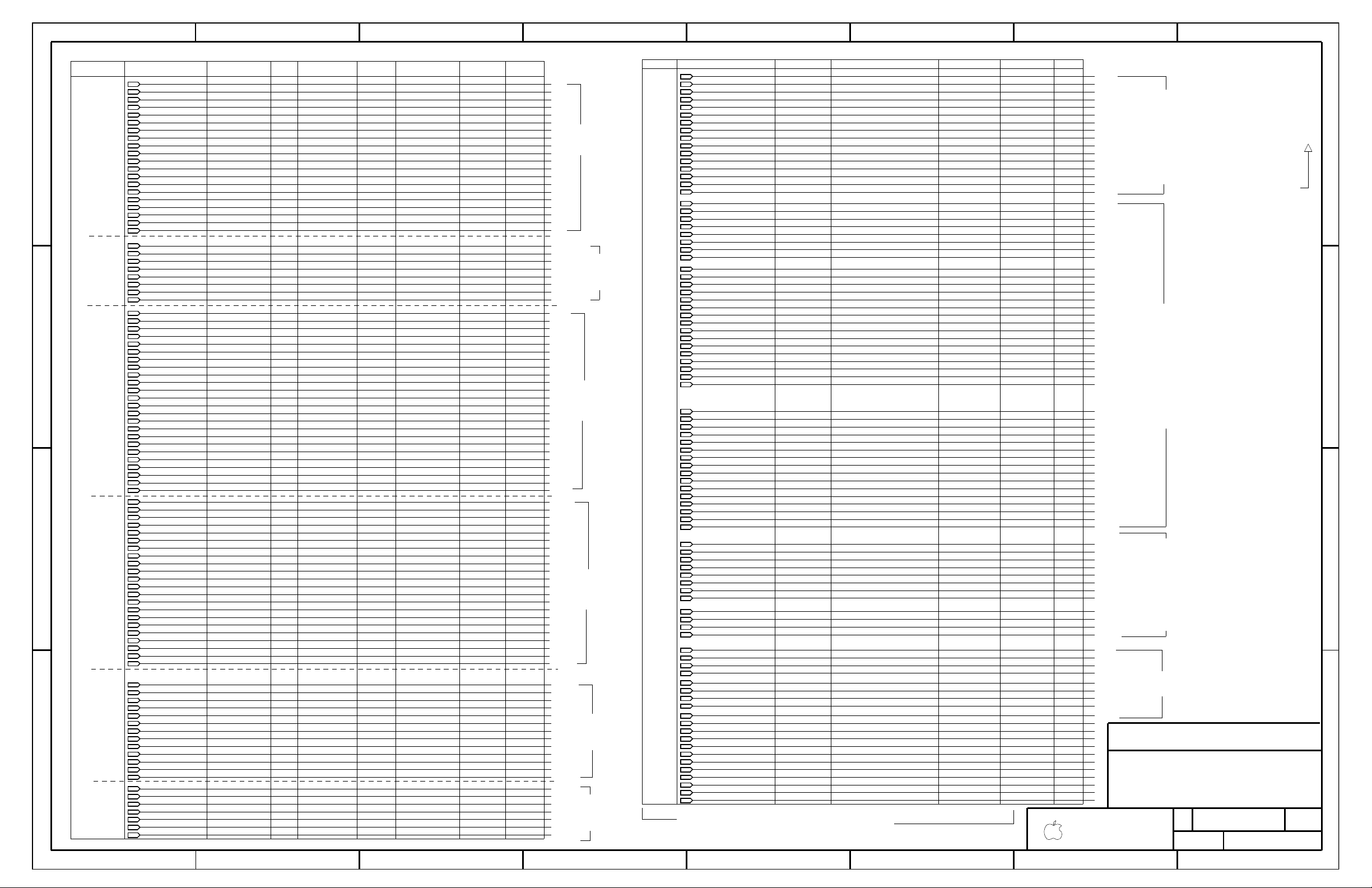
D
SIZE
OF
SHT
DRAWING NUMBER
NOTICE OF PROPRIETARY PROPERTY
I TO MAINTAIN THE DOCUMENT IN CONFIDENCE
III NOT TO REVEAL OR PUBLISH IN WHOLE OR PART
II NOT TO REPRODUCE OR COPY IT
AGREES TO THE FOLLOWING
PROPERTY OF APPLE COMPUTER, INC. THE POSSESSOR
THE INFORMATION CONTAINED HEREIN IS THE PROPRIETARY
1
2
3
4
5
67
8
12
3
4
5
6
78
B
C
D
A
B
C
D
A
REV.
APPLE COMPUTER INC.
SCALE
NONE
UPPER
PRIORITY: 6
Zo(single) = 55.4 OHMS
Zo(diff) = 106.2 OHMS
T = 0.6MIL (TRACE THICKNESS)
H = 16.8MIL (DIST BETW PLANES)
S = 11MIL (TRACE SEPERATION)
W = 3MIL (TRACE WIDTH)
Er = 4.3 (DIELECTRIC CONSTANT)
T = 0.6MIL (TRACE THICKNESS)
H = 9.6MIL (DIST BETW PLANES)
S = 4.9MIL (TRACE SEPERATION)
W = 3.1MIL (TRACE WIDTH)
T = 0.6MIL (TRACE THICKNESS)
H = 9.6MIL (DIST BETW PLANES)
S = 7MIL (TRACE SEPERATION)
W = 3.6MIL (TRACE WIDTH)
Zo(single) = 46.6 OHMS
Zo(diff) = 89.8 OHMS
Zo(single) = 50 OHMS
Zo(diff) = 94 OHMS
Zo will be lower due to
Clear adjacent power plane!
LAYERS 4 OR 7
DIFFERENTIAL_PAIR
Differential Signals
Er = 4.3 (DIELECTRIC CONSTANT)
LVDS
POWER
LAYERS 4 OR 7
LAYERS 2 OR 9
PRIMARY
LAYERS 4 OR 7
LOWER
Zo = 100
Er = 4.3 (DIELECTRIC CONSTANT)
MAX_EXPOSED_LENGTH
NEED TO MATCH DELAY TO 250
(200)
(200)
(200)
(250)
(250)
(250)
(250)
(350)
(350)
(200)
(200)
(200)
(200)
(200)
(200)
(200)
(200)
(200)
(200)
(200)
(200)
(200)
(200)
(200)
(200)
STUB_LENGTH
PRIORITY: 8
PRIORITY: 7
AGP BYTES 0-1
AGP BYTES 2-3
AGP CONTROL
ULTRA ATA-100
INTREPID
OPTICAL
FIREWIRE MII
EIDE
PCI
AGP
SIG_NAME
NET_SPACING_TYPE
NO_TEST
PULSE_PARAM
SIGNAL CONSTRAINTS - PAGE 2
MAX_VIAS
MAX_EXPOSED_LENGTH
Zo = 110
FIREWIRE
GROUP
Zo = 100
ETHERNET
Zo = 90
USB 1.1
Zo = 90
USB 2.0
THERMOSTAT
SUPPLIES
PRIMARY LAYERS: 9
SECONDARY LAYERS: 4,7
SECONDARY
LAYERS: 2,9
LAYERS: 2,9
LAYERS: 4,7
SECONDARY
PRIMARY
PRIMARY
SECONDARY
LAYERS: 2,9
LAYERS: 2,9
LAYERS: 4,7
SECONDARY
PRIMARY
LAYERS: 2,9
LAYERS: 4,7
SECONDARY
PRIMARY
PRIORITY: 3
PRIMARY LAYERS: 4,7 FOR CONTROLLED IMPEDANCE DIFF PAIRS
SECONDARY LAYERS: 2,9 FOR UNCONTROLLED IMPEDANCE DIFF PAIRS
PRIORITY: 4
PRIORITY: 5
PRIORITY: 5
asymmetric stackup.
(200)
(400)
(400)
(400)
(400)
(400)
(400)(400)
(400)
GROUP
AGP SIDEBAND
SIG_NAME
RELATIVE_PROPAGATION_DELAY
(200)
(200)
PROPAGATION_DELAY
MAX_VIAS
TOTAL UIDE+HD SKEW <500MIL
(200)
ETHERNET MII
Zo = 100
TMDS
LAYERS: 4,7
GOAL: MINIMIZE TH VIAS
LAYERS: 4,7
Digital Signals (cont’d)
NET_SPACING_TYPE
I233
I234
I235
I236
I237
I238
I239
I240
I241
I242
I243
I244
051-6338
37 40
C
FW_TPO0P
110 OHM SPACING
500.0000
FW_TPO0
FW_TPO0:G:L:S:0 MIL:5 MIL
FW_TPO0:G:L:S:0 MIL:5 MIL
FW_TPO0N
FW_TPO0
110 OHM SPACING
500.0000
FW_TPI0P
FW_TPI0:G:L:S:0 MIL:5 MIL
FW_TPI0
500.0000
110 OHM SPACING
FW_TPBI0P
FW_TPBI0:G:L:S:0 MIL:5 MIL
FW_TPBI0
110 OHM SPACING
500.0000
FW_TPI0N
500.0000
110 OHM SPACINGFW_TPI0:G:L:S:0 MIL:5 MIL
FW_TPI0
FW_TPBI0N
FW_TPBI0:G:L:S:0 MIL:5 MIL
FW_TPBI0
110 OHM SPACING
500.0000
FW_TPAO0P
FW_TPAO0:G:L:S:0 MIL:5 MIL
FW_TPAO0 500.0000
110 OHM SPACING
FW_TPAO0N
FW_TPAO0:G:L:S:0 MIL:5 MIL
FW_TPAO0 500.0000
110 OHM SPACING
FW_TPO1:G:L:S:0 MIL:4%
FW_TPO1
500.0000
110 OHM SPACING
FW_TPO1P
FW_TPI1:G:L:S:0 MIL:4%
500.0000
110 OHM SPACING
FW_TPI1P
FW_TPI1
FW_TPO1:G:L:S:0 MIL:4%
110 OHM SPACING
FW_TPO1N
FW_TPO1
500.0000
FW_TPB1:G:L:S:0 MIL:4%
500.0000
FW_TPB1
110 OHM SPACING
FW_TPB1P
FW_TPI1N
FW_TPI1
FW_TPI1:G:L:S:0 MIL:4%
500.0000
110 OHM SPACING
FW_TPB1
FW_TPB1N
FW_TPB1:G:L:S:0 MIL:4%
500.0000
110 OHM SPACING
FW_TPA1:G:L:S:0 MIL:4%
FW_TPA1
500.0000
110 OHM SPACING
FW_TPA1N
FW_TPA1P
FW_TPA1:G:L:S:0 MIL:4%
FW_TPA1
500.0000
110 OHM SPACING
100 OHM SPACING
100 OHM SPACING
LVDS:G:L:S:0 MIL:110 MIL
LVDS_U1P
500.0000
LVDS_U1
100 OHM SPACING
100 OHM SPACING
ATITMDS:G:L:S:0 MIL:50 MIL
200.0000
8
ATI_TMDS_D1
ATI_TMDS_DP<1>
100 OHM SPACING
100 OHM SPACING
ATI_TMDS_DN<0>
200.0000
ATI_TMDS_D08ATITMDS:G:L:S:0 MIL:50 MIL
USB_DE:G:L:S:0 MIL:200 MIL
10 MIL SPACING
USB_DEM
USB_DE
100 OHM SPACING
TMDS:G:L:S:0 MIL:50 MIL
CLKTMDS
100 OHM SPACING
5
TMDS_CLKN
500.0000
LVDS:G:L:S:0 MIL:110 MIL
LVDS_L0
100 OHM SPACING
100 OHM SPACING
500.0000
LVDS_L0P
500.0000
100 OHM SPACING
100 OHM SPACING
LVDS:G:L:S:0 MIL:110 MIL
LVDS_L1
LVDS_L1P
TMDS:G:L:S:0 MIL:50 MIL
100 OHM SPACING
100 OHM SPACING
TMDS_DN<0>
500.0000
8
TMDS_D0
100 OHM SPACING
100 OHM SPACING
TMDS_D1
500.0000
8
TMDS:G:L:S:0 MIL:50 MIL
TMDS_DP<1>
L:S:1050:1450
66 MHz
7
AGP_SBA<7..0>
100 OHM SPACING
100 OHM SPACING
500.0000
4
CLKLVDS_L
CLKLVDS_LN
LVDS:G:L:S:0 MIL:110 MIL
100 OHM SPACING
LVDS:G:L:S:0 MIL:110 MIL
100 OHM SPACING
500.0000
LVDS_L2
LVDS_L2N
LVDS:G:L:S:0 MIL:110 MIL
100 OHM SPACING
100 OHM SPACING
LVDS_L0N
500.0000
LVDS_L0
200.0000
100 OHM SPACING
100 OHM SPACING
ATITMDS:G:L:S:0 MIL:50 MIL
ATI_TMDS_D0
ATI_TMDS_DP<0>
8
8 MIL SPACING
6
133.0 MHz:::
L:S:1050 MIL:1450 MIL
AGP_AD_STB<1>
100 OHM SPACING
100 OHM SPACING
500.0000
ATITMDS:G:L:S:0 MIL:50 MIL
ATI_TMDS_D2
8
ATI_TMDS_DP<2>
100 OHM SPACING
100 OHM SPACING
ATITMDS:G:L:S:0 MIL:50 MIL
500.0000
8
ATI_TMDS_DN<2>
ATI_TMDS_D2
100 OHM SPACING
100 OHM SPACING
TMDS:G:L:S:0 MIL:50 MIL
TMDS_D2
500.0000
TMDS_DN<2>
8
CLKLVDS_L
100 OHM SPACING
100 OHM SPACING
500.0000
LVDS:G:L:S:0 MIL:110 MIL
4
CLKLVDS_LP
ATI_CLKTMDS
100 OHM SPACING
100 OHM SPACING
ATI_TMDS_CLKN
200.0000
5
ATITMDS:G:L:S:0 MIL:50 MIL
500.0000
LVDS_U2
100 OHM SPACING
100 OHM SPACING
LVDS:G:L:S:0 MIL:110 MIL
LVDS_U2N
LVDS_U1N
100 OHM SPACING
100 OHM SPACING
LVDS:G:L:S:0 MIL:110 MIL
500.0000
LVDS_U1
7
66 MHz
L:S:1050:1450
AGP_AD<15..0>
ENET_MDI3:G:U43.43:J23.10:0 MIL:100 MIL
ENET 10 MIL SPACING
MDI_M<3>
ENET_MDI3
ENET 10 MIL SPACING
ENET 10 MIL SPACING
ENET_MDI2:G:U43.41:J23.8:0 MIL:100 MIL
ENET 10 MIL SPACING
ENET_MDI2
MDI_M<2>
ENET 10 MIL SPACING
ENET_MDI0:G:U43.31:J23.2:0 MIL:100 MIL
ENET_MDI0
ENET 10 MIL SPACING
MDI_M<0>
ENET 10 MIL SPACING
ENET 10 MIL SPACING
ENET_MDI2:G:U43.39:J23.7:0 MIL:100 MIL
MDI_P<2>
ENET_MDI2
ENET 10 MIL SPACING
ENET_MDI1:G:U43.33:J23.3:0 MIL:100 MIL
MDI_P<1>
ENET_MDI1
ENET 10 MIL SPACING
U51.V1:RP19.3::600 MIL
100.0 MHz:::
UIDE_DATA<7>
USB_D1:G:L:S:0 MIL:20 MIL
500.0000
NEC_USB_DAP
USB_D1
90 OHM SPACING
90 OHM SPACING
NEC_USB_DAM
USB_D1 500.0000
USB_D1:G:L:S:0 MIL:20 MIL
EIDE_OPTICAL_READ_L
L:S:4500 MIL:6500 MIL
33.00 MHz:::
ENET_MDC
L:S:8000 MIL:9000 MIL
FW_LINK_DATA<7..0>
7
L:S:2700:3500
L:S:8000 MIL:9000 MIL
ENET_RX_DV
EIDE_OPTICAL_ADDR<2..0>
33 MHZ
L:S:4000:6000
L:S::500 MIL
EIDE_RD_L
33.00 MHz:::
EIDE_CS0_L
L:S::850 MIL 33.00 MHz:::
EIDE_ADDR<2..0>
33 MHZL:S::850
33 MHZL:S::850
EIDE_DATA<15..0>
HD_DATA<15..0>
7
100 MHZ
L:S:5000:6500
UIDE_CS1_L
L:S::500 MIL 100.0 MHz:::
L:S::400 MIL 100.0 MHz:::
UIDE_RST_L
100 MHZ
UIDE_DATA<15..8>
L:S::710
THERM1:G:L:S:0 MIL:100 MIL
THERM1_DM
5V_SNSP
5V_SNS
5V_SNS:G:L:S:0 MIL:100 MIL
THERM1_DP
THERM1:G:L:S:0 MIL:100 MIL
1772_CSI
1772_CSI:G:L:S:0 MIL:100 MIL
1772_CSIP
LVDS:G:L:S:0 MIL:110 MIL
100 OHM SPACING
100 OHM SPACING
LVDS_L1N
500.0000
LVDS_L1
66 MHz
7
L:S:1050:1450
AGP_CBE<1..0>
HD_IOCHRDY
10 MIL SPACING
L:S:6200 MIL:6300 MIL
7
100.0 MHz:::
HD_DIOR_L
L:S:6100 MIL:6150 MIL
100.0 MHz:::
7
10 MIL SPACING
100 MHZ
L:S::650
UIDE_ADDR<2..0>
UIDE_DMACK_L
100.0 MHz:::L:S::400 MIL
7
100.0 MHz:::
HD_CS0_L
L:S:3000 MIL:6000 MIL
HD_CS1_L
100.0 MHz:::
7
L:S:3000 MIL:6000 MIL
7
L:S:3000 MIL:5000 MIL
100.0 MHz:::
HD_INTRQ
33 MHz
MIN_DAISY_CHAIN
L:S:6000:12500
PCI_AD<31..0>
5V_SNSM
5V_SNS
5V_SNS:G:L:S:0 MIL:100 MIL
8 MIL SPACING
133.0 MHz:::
6
L:S:1050 MIL:1450 MIL
AGP_AD_STB_L<1>
L:S:1250 MIL:1950 MIL
6
66.00 MHz:::
AGP_RBF_L
L:S:1250 MIL:1950 MIL
6
66.00 MHz:::
AGP_GNT_L
66 MHz
7
L:S:1050:1450
AGP_CBE<3..2>
8 MIL SPACING
L:S:1050 MIL:1450 MIL
6
66.00 MHz:::
AGP_SB_STB
L:S:6000 MIL:12500 MIL
MIN_DAISY_CHAIN
33.00 MHz:::
PCI_STOP_L
L:S:1250 MIL:1950 MIL
6
66.00 MHz:::
AGP_IRDY_L
ENET_LINK_TX_EN
L:S::400 MIL
8 MIL SPACING
133.0 MHz:::
6
L:S:1050 MIL:1450 MIL
AGP_AD_STB<0>
FW_PHY_DATA<7..0>
7
L:S:4700:5500
ENET_PHY_TXD<7..0>
7
L:S:8000:9000
ENET_LINK_RXD<7..0>
7
L:S:8000:9000
EIDE_OPTICAL_DATA<15..0>
33 MHZ
L:S:4000:6000
ENET_LINK_TXD<7..0>
L:S::600
FW_LINK_CNTL<1..0>
L:S:9000:10000
FW_PHY_CNTL<1..0>
L:S::300
1772_CSSP
1772_CSS
1772_CSS:G:L:S:0 MIL:100 MIL
3V_SNSP
3V_SNS
3V_SNS:G:L:S:0 MIL:100 MIL
EIDE_DMACK_L
L:S::500 MIL 33.00 MHz:::
EIDE_DMARQ
L:S::500 MIL 33.00 MHz:::
EIDE_INT
L:S::500 MIL 33.00 MHz:::
EIDE_OPTICAL_CS0_L
L:S:4500 MIL:6500 MIL
33.00 MHz:::
EIDE_OPTICAL_CS1_L
L:S:4500 MIL:6500 MIL
33.00 MHz:::
EIDE_OPTICAL_DMAACK_L
L:S:4500 MIL:6500 MIL
33.00 MHz:::
EIDE_OPTICAL_DMA_RQ
L:S:4500 MIL:6500 MIL
33.00 MHz:::
EIDE_OPTICAL_INT
L:S:5000 MIL:7000 MIL
33.00 MHz:::
EIDE_OPTICAL_IOCHRDY
L:S:4500 MIL:6500 MIL
33.00 MHz:::
EIDE_OPTICAL_RST_L
L:S:4500 MIL:6500 MIL
33.00 MHz:::
EIDE_OPTICAL_WR_L
L:S:4500 MIL:6500 MIL
33.00 MHz:::
ENET_COL
L:S:8000 MIL:9000 MIL
ENET_CRS
L:S:8000 MIL:9000 MIL
ENET_LINK_TX_ER
L:S::400 MIL
ENET_MDIO
L:S:8000 MIL:9000 MIL
ENET_PHY_TX_EN
7
L:S:8000 MIL:9000 MIL
ENET_PHY_TX_ER
7
L:S:8000 MIL:9000 MIL
ENET_RX_ER
L:S:8000 MIL:9000 MIL
FW_LINK_LREQ
L:S::300 MIL
FW_PHY_LREQ
L:S:8500 MIL:9500 MIL
FW_PINT
L:S:8500 MIL:9500 MIL
L:S:6000 MIL:12500 MIL
33.00 MHz:::
MIN_DAISY_CHAIN
PCI_TRDY_L
THERM1_ALT
THERM1_ALT:G:L:S:0 MIL:100 MIL
THERM1_A_DM
THERM1_ALT
THERM1_A_DP
THERM1_ALT:G:L:S:0 MIL:100 MIL
THERM1_MAIN
THERM1_MAIN:G:L:S:0 MIL:100 MIL
THERM1_M_DM
THERM1_MAIN
THERM1_M_DP
THERM1_MAIN:G:L:S:0 MIL:100 MIL
THERM2_ALT
THERM2_A_DM
THERM2_ALT:G:L:S:0 MIL:100 MIL
THERM2_ALT
THERM2_A_DP
THERM2_ALT:G:L:S:0 MIL:100 MIL
THERM2_DM
THERM2:G:L:S:0 MIL:100 MIL
THERM2_DP
THERM2:G:L:S:0 MIL:100 MIL
THERM2_MAIN
THERM2_M_DM
THERM2_MAIN:G:L:S:0 MIL:100 MIL
THERM2_MAIN
THERM2_M_DP
THERM2_MAIN:G:L:S:0 MIL:100 MIL
UIDE_CS0_L
100.0 MHz:::L:S::500 MIL
L:S:6000 MIL:12500 MIL
MIN_DAISY_CHAIN
33.00 MHz:::
PCI_DEVSEL_L
EIDE_CS1_L
L:S::850 MIL 33.00 MHz:::
L:S:1250 MIL:1950 MIL
6
66.00 MHz:::
AGP_TRDY_L
7
66.00 MHz:::
L:S:1250 MIL:1950 MIL
AGP_DEVSEL_L
L:S:1250 MIL:1950 MIL
6
66.00 MHz:::
AGP_STOP_L
6
66.00 MHz:::
L:S:1250 MIL:1950 MIL
AGP_PAR
100 MHZ
UIDE_DATA<6..0>
L:S::600
100.0 MHz:::
HD_DMACK_L
7
L:S:4500 MIL:6000 MIL
L:S:3000 MIL:5200 MIL
HD_DIOW_L
7
100.0 MHz:::
EIDE_WR_L
33.00 MHz:::L:S::500 MIL
10 MIL SPACING
UIDE_DIOR_L
100.0 MHz:::L:S::600 MIL
UIDE_DMARQ
L:S::400 MIL 100.0 MHz:::
100 MHZ
HD_ADDR<2..0>
7
L:S:5000:6500
8 MIL SPACING
6
66.00 MHz:::
L:S:1050 MIL:1450 MIL
AGP_SB_STB_L
L:S:1250 MIL:1950 MIL
6
66.00 MHz:::
AGP_REQ_L
MIN_DAISY_CHAIN
33.00 MHz:::
L:S:6000 MIL:12500 MIL
PCI_FRAME_L
33 MHz
MIN_DAISY_CHAIN
L:S:6000:12500
PCI_CBE<3..0>
100.0 MHz:::
7
HD_DMARQ
L:S:4500 MIL:6000 MIL
1772_CSIN
1772_CSI
1772_CSI:G:L:S:0 MIL:100 MIL
100 OHM SPACING
100 OHM SPACING
LVDS:G:L:S:0 MIL:110 MIL
500.0000
4
CLKLVDS_U
CLKLVDS_UN
1772_CSS
1772_CSS:G:L:S:0 MIL:100 MIL
1772_CSSN
3V_SNS
3V_SNS:G:L:S:0 MIL:100 MIL
3V_SNSM
L:S:4000 MIL:6000 MIL
7
HD_RESET_L
100.0 MHz:::
UIDE_INTRQ
100.0 MHz:::L:S::400 MIL
133.0 MHz:::
6
8 MIL SPACING
L:S:1050 MIL:1450 MIL
AGP_AD_STB_L<0>
66 MHz
7
L:S:1050:1450
AGP_AD<31..16>
66.00 MHz:::
L:S:1250 MIL:1950 MIL
6
AGP_FRAME_L
MIN_DAISY_CHAIN
L:S:6000 MIL:12500 MIL
33.00 MHz:::
PCI_IRDY_L
L:S:6000 MIL:12500 MIL
33.00 MHz:::
MIN_DAISY_CHAIN
PCI_PAR
UIDE_DIOW_L
100.0 MHz:::L:S::400 MIL
UIDE_IOCHRDY
100.0 MHz:::
10 MIL SPACING
L:S::600 MIL
EIDE_IOCHRDY
L:S::500 MIL 33.00 MHz:::
EIDE_RST_L
L:S::500 MIL 33.00 MHz:::
TMDS_DP<2>
100 OHM SPACING
100 OHM SPACING
TMDS_D2
500.0000
8
TMDS:G:L:S:0 MIL:50 MIL
ATITMDS:G:L:S:0 MIL:50 MIL
ATI_TMDS_D1
100 OHM SPACING
100 OHM SPACING
200.0000
8
ATI_TMDS_DN<1>
BT_USB:G:L:S:0 MIL:200 MIL
10 MIL SPACING
BT_USB_DM
BT_USB_D
MODEM_USB_D
MODEM_USB:G:L:S:0 MIL:200 MIL
10 MIL SPACING
MODEM_USB_DP
MODEM_USB_DM
MODEM_USB:G:L:S:0 MIL:200 MIL
MODEM_USB_D
10 MIL SPACING
BT_USB_DP
BT_USB_D
10 MIL SPACING
BT_USB:G:L:S:0 MIL:200 MIL
USB_D2:G:L:S:0 MIL:20 MIL
500.0000
90 OHM SPACING
NEC_USB_DBM
USB_D2
USB_D2:G:L:S:0 MIL:20 MIL
500.0000
NEC_USB_DBP
USB_D2
90 OHM SPACING
100 OHM SPACING
LVDS:G:L:S:0 MIL:110 MIL
100 OHM SPACING
500.0000
LVDS_U0
LVDS_U0P
ENET 10 MIL SPACING
ENET_MDI3:G:U43.42:J23.9:0 MIL:100 MIL
ENET_MDI3
MDI_P<3>
ENET 10 MIL SPACING
ENET 10 MIL SPACING
ENET_MDI1:G:U43.34:J23.4:0 MIL:100 MIL
ENET_MDI1
MDI_M<1>
ENET 10 MIL SPACING
ENET 10 MIL SPACING
ENET_MDI0:G:U43.29:J23.1:0 MIL:100 MIL
MDI_P<0>
ENET_MDI0
ENET 10 MIL SPACING
USB_DF
USB_DF:G:L:S:0 MIL:200 MIL
USB_DFM
10 MIL SPACING
USB_DE:G:L:S:0 MIL:200 MIL
USB_DE
10 MIL SPACING
USB_DEP
ATITMDS:G:L:S:0 MIL:50 MIL
ATI_CLKTMDS
100 OHM SPACING
100 OHM SPACING
200.0000
5
ATI_TMDS_CLKP
USB_DF
USB_DF:G:L:S:0 MIL:200 MIL
10 MIL SPACING
USB_DFP
100 OHM SPACING
TMDS:G:L:S:0 MIL:50 MIL
100 OHM SPACING
TMDS_DP<0>
500.0000
8
TMDS_D0
TMDS:G:L:S:0 MIL:50 MIL
100 OHM SPACING
100 OHM SPACING
5
CLKTMDS
500.0000
TMDS_CLKP
500.0000
TMDS:G:L:S:0 MIL:50 MIL
8
100 OHM SPACING
100 OHM SPACING
TMDS_DN<1>
TMDS_D1
LVDS_U2P
100 OHM SPACING
100 OHM SPACING
LVDS:G:L:S:0 MIL:110 MIL
500.0000
LVDS_U2
100 OHM SPACING
100 OHM SPACING
LVDS:G:L:S:0 MIL:110 MIL
500.0000
LVDS_L2
LVDS_L2P
500.0000
LVDS:G:L:S:0 MIL:110 MIL
100 OHM SPACING
100 OHM SPACING
CLKLVDS_UP
4
CLKLVDS_U
100 OHM SPACING
100 OHM SPACING
LVDS:G:L:S:0 MIL:110 MIL
500.0000
LVDS_U0N
LVDS_U0
39 24
39
39
39
39
39
39
18
24
24
24
24
24
24
24
39
39
39
39
39
39
39
39
39
39
39
39
39
39
39
39
17
18
18
18
18
18
18
18
39
39
39
39
39
39
39
39
39
39
28
28
28
28
39
39
39
28
39
28
28
28
22
22
22
22
22
22
19
22
22
22
19
22
22
22
22
19
39
39
39
39
39
24
25
25
39
26
27
26
39
24
24
24
24
24
24
24
22
19
24
24
24
12
19
19
19
19
19
17
19
19
26
26
39
27
24
24
24
39
39
39
39
39
39
39
39
26
26
26
26
26
26
27
27
17
24
17
24
19
19
19
19
24
24
24
19
19
17
17
24
22
19
19
19
17
17
24
24
24
24
22
25
25
25
25
25
25
22
39
39
39
22
22
22
22
22
22
22
27
27
27
28
27
28
28
28
28
28
28
27
28
27
27
27
20
20
20
14
19
20
20
19
19
12
20
20
20
20
12
20
20
19
20
20
20
20
12
26
26
26
26
26
13
17
17
24
13
13
13
24
13
13
13
13
24
13
13
13
25
32
25
30
20
12
24
24
13
13
24
24
13
9
32
12
12
12
12
12
12
12
13
12
27
13
13
24
13
13
27
30
32
13
13
13
24
24
24
24
24
24
24
24
13
13
13
13
13
13
13
13
13
13
12
25
25
25
25
25
25
25
25
25
25
13
12
13
12
12
12
12
13
24
24
13
13
13
24
12
12
12
12
13
30
20
30
32
24
13
12
12
12
12
12
13
13
13
13
19
20
14
14
14
14
17
17
20
26
26
26
14
14
20
14
19
19
19
20
20
20
20
Page 38

IN
IN
IN
IN
IN
D
SIZE
OF
SHT
DRAWING NUMBER
NOTICE OF PROPRIETARY PROPERTY
I TO MAINTAIN THE DOCUMENT IN CONFIDENCE
III NOT TO REVEAL OR PUBLISH IN WHOLE OR PART
II NOT TO REPRODUCE OR COPY IT
AGREES TO THE FOLLOWING
PROPERTY OF APPLE COMPUTER, INC. THE POSSESSOR
THE INFORMATION CONTAINED HEREIN IS THE PROPRIETARY
1
2
3
4
5
67
8
12
3
4
5
6
78
B
C
D
A
B
C
D
A
REV.
APPLE COMPUTER INC.
SCALE
NONE
ETHERNET
88E1111
NEC USB2.0
POWER NET CONSTRAINTS
MAX1717
2.5V SWITCHER
INVERTER
I/O AREA
ADAPTER
CHARGER
BATTERY
MIN_NECK_WIDTHMIN_LINE_WIDTHVOLTAGE
SIG_NAME
GROUP
PLLS
REFERENCE
HALL EFFECT
HD
TRACKPAD
PMU
LVDS
TRACKPAD
LTC3707
5V SWITCHER
3V SWITCHER
MIN_LINE_WIDTHVOLTAGE
GROUP
SIG_NAME
MIN_NECK_WIDTHMIN_LINE_WIDTHVOLTAGE
SIG_NAME
14V SWITCHER
GROUP
LTC1625
CONTROL
LTC1778
SIGNAL CONSTRAINTS - PAGE 3
LTC3411
LTC1962
INT PLLS
CPU
INTREPID
MIN_NECK_WIDTH
MAX1715
CARDBUS
AIRPORT
DDR RAM
VIDEO
FAN
AUDIO
MISC
FW
ATI M10
MAIN/SLEEP
1.65V SWITCHER
I308
I310
I311
I312
I314
I315
I316
I317
CHGND1
CHGND2
CHGND3
CHGND4
I332
I333
I345
I346
I347
I348
I349
I350
I351
I352
I353
I354
I355
I356
I357
I358
I359
I360
I361
C
4038
051-6338
VOLTAGE=0V
MIN_LINE_WIDTH=25
MIN_NECK_WIDTH=6
VOLTAGE=0V
MIN_NECK_WIDTH=12MIN_LINE_WIDTH=25
MIN_NECK_WIDTH=12MIN_LINE_WIDTH=25
VOLTAGE=0V
VOLTAGE=0V
MIN_LINE_WIDTH=25 MIN_NECK_WIDTH=12
MIN_NECK_WIDTH=12MIN_LINE_WIDTH=25
VOLTAGE=0V
MIN_NECK_WIDTH=6
VOLTAGE=1.5V
MIN_LINE_WIDTH=10
+1_5V_INTREPID_PLL3
MIN_NECK_WIDTH=10MIN_LINE_WIDTH=25
VOLTAGE=1.5V
+1_5V_SLEEP_VIN
MIN_NECK_WIDTH=10
VOLTAGE=1.5V
MIN_LINE_WIDTH=25
+1_5V_MAIN
MIN_NECK_WIDTH=10MIN_LINE_WIDTH=25
VOLTAGE=1.5V
+1_5V_SLEEP
VOLTAGE=1.5V
MIN_LINE_WIDTH=25 MIN_NECK_WIDTH=10
+1_5V_LDO
MIN_LINE_WIDTH=25
VOLTAGE=1.8V
MIN_NECK_WIDTH=10
+1_8V_SLEEP
MIN_NECK_WIDTH=6
VOLTAGE=1.8V
MIN_LINE_WIDTH=25
+1_8V_MAIN
VOLTAGE=2.5V
MIN_LINE_WIDTH=25 MIN_NECK_WIDTH=10
+2_5V_MAIN
MIN_LINE_WIDTH=25
VOLTAGE=2.5V
MIN_NECK_WIDTH=10
+2_5V_SLEEP
MIN_NECK_WIDTH=10MIN_LINE_WIDTH=25
VOLTAGE=3.3V
+3V_PMU
VOLTAGE=3.3V
MIN_LINE_WIDTH=25 MIN_NECK_WIDTH=10
+3V_MAIN
MIN_NECK_WIDTH=10
VOLTAGE=1.8V
MIN_LINE_WIDTH=15
+1_8V_GPU_TP_PLL
VOLTAGE=1.8V
MIN_NECK_WIDTH=10MIN_LINE_WIDTH=20
+1_8V_ATI_TPVDD
MIN_LINE_WIDTH=15
VOLTAGE=1.8V
MIN_NECK_WIDTH=10
+1_8V_GPU_PLL
MIN_NECK_WIDTH=10MIN_LINE_WIDTH=10
VOLTAGE=1.8V
+1_8V_GPU_AVDDQ
VOLTAGE=1.2V
MIN_LINE_WIDTH=30 MIN_NECK_WIDTH=10
GPU_VCORE
VOLTAGE=1.8V
MIN_NECK_WIDTH=10MIN_LINE_WIDTH=20
+1_8V_ATI_PVDD
VOLTAGE=1.5V
MIN_LINE_WIDTH=20 MIN_NECK_WIDTH=10
+1_5V_AGP_GPU
MIN_NECK_WIDTH=10MIN_LINE_WIDTH=25
VOLTAGE=2.5V
GPU_MEM_IO_FLT
MIN_NECK_WIDTH=10
VOLTAGE=1.8V
MIN_LINE_WIDTH=25
+1_8V_GPU
MIN_NECK_WIDTH=10
VOLTAGE=2.5V
MIN_LINE_WIDTH=30
+2_5V_GPU
VOLTAGE=3.3V
MIN_NECK_WIDTH=10MIN_LINE_WIDTH=25
+3V_GPU_FLT
VOLTAGE=1.5V
MIN_NECK_WIDTH=10MIN_LINE_WIDTH=20
+1_5V_GPU_VDD15
MIN_LINE_WIDTH=10
VOLTAGE=1.8V
MIN_NECK_WIDTH=10
+1_8V_GPU_MEMPLL
MIN_LINE_WIDTH=25 MIN_NECK_WIDTH=10
VOLTAGE=2.5V
+2_5V_GPU_MEMCORE
VOLTAGE=12.8V
MIN_LINE_WIDTH=100
MIN_NECK_WIDTH=12
FW_VDD_ON
MIN_NECK_WIDTH=12
MIN_LINE_WIDTH=100
VOLTAGE=12.8V
+FW_AMP_SENSE
MIN_LINE_WIDTH=25
VOLTAGE=3.3V
MIN_NECK_WIDTH=10
+3V_FW
VOLTAGE=33V
MIN_LINE_WIDTH=100
MIN_NECK_WIDTH=12
+FW_PWR1
VOLTAGE=1.95V
MIN_LINE_WIDTH=25 MIN_NECK_WIDTH=10
+1_95V_FW_DVDD_PORT1
VOLTAGE=1.95V
MIN_NECK_WIDTH=10MIN_LINE_WIDTH=25
+1_95V_FW_DVDD
MIN_LINE_WIDTH=25
VOLTAGE=3.3V
MIN_NECK_WIDTH=10
+3V_FW_AVDD_PORT2
MIN_LINE_WIDTH=100
VOLTAGE=33V
MIN_NECK_WIDTH=12
+FW_PWR_OR
VOLTAGE=33V
MIN_LINE_WIDTH=100
MIN_NECK_WIDTH=12
+FW_VP1
VOLTAGE=5V
MIN_NECK_WIDTH=10MIN_LINE_WIDTH=25
+FAN_PWR
MIN_LINE_WIDTH=25
VOLTAGE=0V
TV_GND2
MIN_LINE_WIDTH=25
VOLTAGE=0V
GPU_TV_GND2
MIN_LINE_WIDTH=25
VOLTAGE=0V
TV_GND1
MIN_LINE_WIDTH=12
VOLTAGE=3.3V
MIN_NECK_WIDTH=10
+3V_LCD
MIN_LINE_WIDTH=10
VOLTAGE=24V
+ADAPTER_OR_BATT
MIN_LINE_WIDTH=10
VOLTAGE=12.6V
MIN_NECK_WIDTH=10
+BATT_VSNS
MIN_NECK_WIDTH=10
VOLTAGE=16.8V
MIN_LINE_WIDTH=25
+BATT_POS
MIN_LINE_WIDTH=10
VOLTAGE=1.25V
INT_AGP_VREF
MIN_LINE_WIDTH=10
VOLTAGE=1.2V
GPU_VCORE_NECK
MIN_LINE_WIDTH=8
LTC3411_SYNC
MIN_LINE_WIDTH=8
VCORE_CC
MIN_LINE_WIDTH=8
VCORE_REF
MIN_LINE_WIDTH=8
MAX1715_SKIP
MIN_LINE_WIDTH=25 MIN_NECK_WIDTH=10
VOLTAGE=3.3V
3V_RSNS
VOLTAGE=5V
MIN_LINE_WIDTH=25 MIN_NECK_WIDTH=10
5V_SW
VOLTAGE=14V
MIN_LINE_WIDTH=10
+PBUS_JUMPER
VOLTAGE=0V
MIN_LINE_WIDTH=10
3707_SGND
VOLTAGE=2.5V
MIN_LINE_WIDTH=20 MIN_NECK_WIDTH=10
2_5V_DL
VOLTAGE=5V
MIN_NECK_WIDTH=10MIN_LINE_WIDTH=15
1_5V_BST
VOLTAGE=2.5V
MIN_LINE_WIDTH=20 MIN_NECK_WIDTH=10
2_5V_DH
MIN_NECK_WIDTH=10MIN_LINE_WIDTH=20
VOLTAGE=5V
VCORE_VCC
VOLTAGE=1.95V
MIN_NECK_WIDTH=10MIN_LINE_WIDTH=25
+1_95V_FW_DVDD_RX0
MIN_NECK_WIDTH=10
VOLTAGE=3.3V
MIN_LINE_WIDTH=25
+3V_FW_AVDD_PORT0
VOLTAGE=3.3V
MIN_LINE_WIDTH=25 MIN_NECK_WIDTH=10
+3V_FW_UF
MIN_NECK_WIDTH=10
VOLTAGE=3.3V
MIN_LINE_WIDTH=15
NEC_AVDD
MIN_NECK_WIDTH=10
VOLTAGE=1.0V
MIN_LINE_WIDTH=25
LTC3405_SW
MIN_NECK_WIDTH=10
VOLTAGE=2.5V
MIN_LINE_WIDTH=25
+2_5V_MARVELL
MIN_LINE_WIDTH=25
VOLTAGE=1.0V
MIN_NECK_WIDTH=10
+1_0V_MARVELL
MIN_LINE_WIDTH=10
VOLTAGE=0V
1772_GND
MIN_LINE_WIDTH=10
VOLTAGE=24V
+ADAPTER_ILIM
MIN_LINE_WIDTH=15 MIN_NECK_WIDTH=10
VOLTAGE=5V
2_5V_BST
VOLTAGE=3.3V
MIN_LINE_WIDTH=25 MIN_NECK_WIDTH=10
+3V_MAIN_AUD
MIN_LINE_WIDTH=50
VOLTAGE=0V
AUD_GND
MIN_LINE_WIDTH=25
VOLTAGE=3.3V
MIN_NECK_WIDTH=10
+3V_LCD_SW
MIN_LINE_WIDTH=10
VOLTAGE=4.85V
+4_85V_ESR
VOLTAGE=12.6V
MIN_LINE_WIDTH=25 MIN_NECK_WIDTH=10
+BATT_24V_FUSE
MIN_NECK_WIDTH=6
VOLTAGE=1.5V
MIN_LINE_WIDTH=15
+1_5V_INTREPID_PLL5
MIN_LINE_WIDTH=25 MIN_NECK_WIDTH=10
VOLTAGE=5V
+5V_MAIN_AUD
VOLTAGE=0V
MIN_NECK_WIDTH=10MIN_LINE_WIDTH=25
FAN1_GND
MIN_LINE_WIDTH=25
VOLTAGE=5V
MIN_NECK_WIDTH=10
+5V_INV_SW
MIN_NECK_WIDTH=10MIN_LINE_WIDTH=15
VOLTAGE=5V
+5V_DDC_SLEEP
VOLTAGE=5V
MIN_LINE_WIDTH=25 MIN_NECK_WIDTH=10
+5V_HD_SLEEP
VOLTAGE=24V
MIN_LINE_WIDTH=10
1772_DCIN
MIN_NECK_WIDTH=10MIN_LINE_WIDTH=25
VOLTAGE=5V
+5V_MAIN
MIN_NECK_WIDTH=10
VOLTAGE=0V
MIN_LINE_WIDTH=25
FAN2_GND
MIN_LINE_WIDTH=8
LTC3411_SHDN
MIN_LINE_WIDTH=30 MIN_NECK_WIDTH=10
VOLTAGE=0V
1778_GND
MIN_NECK_WIDTH=10MIN_LINE_WIDTH=20
VCORE_DL
VOLTAGE=3.3V
MIN_LINE_WIDTH=10 MIN_NECK_WIDTH=10
+3V_ATI_OSC_SLEEP
VOLTAGE=5V
MIN_LINE_WIDTH=15 MIN_NECK_WIDTH=10
+5V_DDC_SLEEP_UF
VOLTAGE=3.3V
MIN_LINE_WIDTH=10
+3V_PMU_ESR
MIN_NECK_WIDTH=10MIN_LINE_WIDTH=50
VOLTAGE=24V
+ADAPTER_SENSE
MIN_LINE_WIDTH=50 MIN_NECK_WIDTH=10
VOLTAGE=24V
+ADAPTER
MIN_LINE_WIDTH=8
1778_VRNG
MIN_LINE_WIDTH=8
1778_FCB
MIN_LINE_WIDTH=8
1778_VFB
VOLTAGE=0V
MIN_NECK_WIDTH=10MIN_LINE_WIDTH=30
LTC3411_GND
MIN_LINE_WIDTH=8
1_8V_VFB
VOLTAGE=14V
MIN_NECK_WIDTH=10MIN_LINE_WIDTH=20
1778_VIN
MIN_NECK_WIDTH=10
VOLTAGE=2.5V
MIN_LINE_WIDTH=20
+2_5V_GPU_PNLIO
VOLTAGE=2.5V
MIN_LINE_WIDTH=10 MIN_NECK_WIDTH=10
+2_5V_GPU_MCLK
MIN_NECK_WIDTH=10
VOLTAGE=1.8V
MIN_LINE_WIDTH=15
+1_8V_GPU_PNLIO
VOLTAGE=1.8V
MIN_NECK_WIDTH=10MIN_LINE_WIDTH=15
+1_8V_GPU_AVDD
MIN_NECK_WIDTH=10MIN_LINE_WIDTH=15
VOLTAGE=2.5V
+2_5V_GPU_A2VDD
MIN_NECK_WIDTH=10MIN_LINE_WIDTH=15
VOLTAGE=1.8V
+1_8V_GPU_VDDDI
VOLTAGE=5V
MIN_LINE_WIDTH=25 MIN_NECK_WIDTH=10
+VPP_CBUS_SW
MIN_NECK_WIDTH=10
VOLTAGE=3.3V
MIN_LINE_WIDTH=25
+VCC_CBUS_SW
MIN_LINE_WIDTH=25
VOLTAGE=0V
GPU_TV_GND1
VOLTAGE=3.3V
MIN_NECK_WIDTH=10MIN_LINE_WIDTH=25
+HD_LOGIC_SLEEP
MIN_NECK_WIDTH=10MIN_LINE_WIDTH=25
VOLTAGE=5V
+5V_INV_UF_SW
MIN_LINE_WIDTH=25 MIN_NECK_WIDTH=10
VOLTAGE=12.6V
+BATT_14V_FUSE
VOLTAGE=5.4V
MIN_LINE_WIDTH=10
1772_LDO
VOLTAGE=5.4V
MIN_LINE_WIDTH=10
1772_DLOV
VOLTAGE=3.3V
MIN_LINE_WIDTH=10
+3V_PMU_AVCC
VOLTAGE=12.6V
MIN_NECK_WIDTH=10MIN_LINE_WIDTH=25
+BATT_RSNS
VOLTAGE=2.5V
MIN_NECK_WIDTH=10MIN_LINE_WIDTH=25
+2_5V_INTREPID
MIN_NECK_WIDTH=6
MIN_LINE_WIDTH=25
VOLTAGE=3.3V
+3V_SLEEP
MIN_NECK_WIDTH=10MIN_LINE_WIDTH=25
VOLTAGE=1.8V
MAXBUS_SLEEP
VOLTAGE=3.3V
MIN_LINE_WIDTH=25 MIN_NECK_WIDTH=10
+3V_INTREPID_USB
MIN_LINE_WIDTH=15
VOLTAGE=1.5V
MIN_NECK_WIDTH=10
+1_5V_INTREPID_PLL
VOLTAGE=1.5V
MIN_LINE_WIDTH=15
MIN_NECK_WIDTH=6
+1_5V_INTREPID_PLL1
MIN_LINE_WIDTH=20 MIN_NECK_WIDTH=10
LTC1962_INT_VIN
MIN_LINE_WIDTH=8
LTC3411_ITH
MIN_LINE_WIDTH=8
LTC3411_ITH_RC
MIN_NECK_WIDTH=10
VOLTAGE=1.8V
MIN_LINE_WIDTH=30
1_8V_SW_F
VOLTAGE=1.8V
MIN_NECK_WIDTH=10MIN_LINE_WIDTH=30
1_8V_SW
MIN_NECK_WIDTH=10MIN_LINE_WIDTH=20
VOLTAGE=3.3V
LTC3411_VCC
MIN_LINE_WIDTH=8
1778_ITH_RC
MIN_LINE_WIDTH=8
1778_ITH
MIN_LINE_WIDTH=8
1778_ION
VOLTAGE=5V
MIN_LINE_WIDTH=10
1625_INTVCC
VOLTAGE=5V
MIN_LINE_WIDTH=10
1625_EXTVCC
VOLTAGE=14V
MIN_LINE_WIDTH=25 MIN_NECK_WIDTH=10
1625_VSW
VOLTAGE=24V
MIN_LINE_WIDTH=10
1625_VIN
VOLTAGE=1.2V
MIN_NECK_WIDTH=10MIN_LINE_WIDTH=50
GPU_VCORE_SW_F
VOLTAGE=1.2V
MIN_NECK_WIDTH=10MIN_LINE_WIDTH=50
GPU_VCORE_SW
MIN_NECK_WIDTH=10MIN_LINE_WIDTH=20
1778_BG
VOLTAGE=5V
MIN_NECK_WIDTH=10MIN_LINE_WIDTH=15
1778_BST_RC
MIN_NECK_WIDTH=10MIN_LINE_WIDTH=20
1778_TG
VOLTAGE=5V
MIN_NECK_WIDTH=10MIN_LINE_WIDTH=15
1778_BST
MIN_LINE_WIDTH=30 MIN_NECK_WIDTH=10
VOLTAGE=0V
MAX1715_GND
MIN_LINE_WIDTH=8
MAX1715_TON
MIN_LINE_WIDTH=8
2_5V_ILIM
MIN_LINE_WIDTH=8
1_5V_ILIM
VOLTAGE=1.5V
MIN_LINE_WIDTH=20 MIN_NECK_WIDTH=10
1_5V_DL
VOLTAGE=1.5V
MIN_LINE_WIDTH=20 MIN_NECK_WIDTH=10
1_5V_DH
VOLTAGE=5V
MIN_LINE_WIDTH=15 MIN_NECK_WIDTH=10
1_5V_BOOST
VOLTAGE=1.5V
MIN_NECK_WIDTH=10MIN_LINE_WIDTH=50
1_5V_LX
VOLTAGE=1.5V
MIN_LINE_WIDTH=8
1_5V_FB
VOLTAGE=5V
MIN_LINE_WIDTH=15 MIN_NECK_WIDTH=10
2_5V_BOOST
VOLTAGE=2.5V
MIN_LINE_WIDTH=50 MIN_NECK_WIDTH=10
2_5V_LX
VOLTAGE=2.5V
MIN_LINE_WIDTH=50 MIN_NECK_WIDTH=10
2_5V_LX_F
VOLTAGE=5V
MIN_LINE_WIDTH=25 MIN_NECK_WIDTH=10
5V_RSNS
VOLTAGE=5V
MIN_LINE_WIDTH=25 MIN_NECK_WIDTH=10
+5V_MAIN_JUMPER
VOLTAGE=3.3V
MIN_LINE_WIDTH=25 MIN_NECK_WIDTH=10
3V_SW
MIN_LINE_WIDTH=25 MIN_NECK_WIDTH=10
VOLTAGE=3.3V
+3V_MAIN_JUMPER
VOLTAGE=5V
MIN_NECK_WIDTH=10MIN_LINE_WIDTH=10
3707_INTVCC
MIN_LINE_WIDTH=10
VOLTAGE=0V
1625_SGND
VOLTAGE=1.2V
MIN_LINE_WIDTH=15 MIN_NECK_WIDTH=10
1V20_REF
MIN_LINE_WIDTH=10
VOLTAGE=4.85V
+4_85V_RAW
MIN_LINE_WIDTH=10
VOLTAGE=4.6V
+4_6V_BU
MIN_LINE_WIDTH=10
VOLTAGE=5V
+5V_TPAD_SLEEP
VOLTAGE=24V
MIN_LINE_WIDTH=25 MIN_NECK_WIDTH=10
+24V_PBUS
VOLTAGE=12.6V
MIN_LINE_WIDTH=25 MIN_NECK_WIDTH=10
+BATT
MIN_NECK_WIDTH=10
VOLTAGE=12.8V
MIN_LINE_WIDTH=25
+PBUS
MIN_NECK_WIDTH=6
MIN_LINE_WIDTH=15
VOLTAGE=1.5V
+1_5V_INTREPID_PLL7
MIN_LINE_WIDTH=15
VOLTAGE=1.5V
MIN_NECK_WIDTH=6
+1_5V_INTREPID_PLL8
MIN_NECK_WIDTH=6
MIN_LINE_WIDTH=15
VOLTAGE=1.5V
+1_5V_INTREPID_PLL6
MIN_NECK_WIDTH=10
VOLTAGE=1.4V
MIN_LINE_WIDTH=25
CPU_VCORE_SLEEP
MIN_LINE_WIDTH=25
VOLTAGE=1.4V
MIN_NECK_WIDTH=10
CPU_AVDD
VOLTAGE=1.25V
MIN_LINE_WIDTH=10
INT_MEM_VREF
VOLTAGE=3.3V
MIN_NECK_WIDTH=10MIN_LINE_WIDTH=25
+3V_AIRPORT
MIN_LINE_WIDTH=10
VOLTAGE=0V
INT_MEM_REF_H
VOLTAGE=0V
MIN_LINE_WIDTH=8
UIDE_REF
MIN_NECK_WIDTH=10
MIN_LINE_WIDTH=200
VOLTAGE=1.4V
VCORE_LX
MIN_NECK_WIDTH=10MIN_LINE_WIDTH=15
VOLTAGE=5V
VCORE_BOOST
VOLTAGE=5V
MIN_LINE_WIDTH=15 MIN_NECK_WIDTH=10
VCORE_BST
VOLTAGE=1.4V
MIN_LINE_WIDTH=8
VCORE_FB
MIN_LINE_WIDTH=8
VCORE_TIME
MIN_LINE_WIDTH=8
VCORE_VGATE
VOLTAGE=0V
MIN_LINE_WIDTH=30
VCORE_GND
MIN_LINE_WIDTH=8
VOLTAGE=0V
VCORE_GNDSNS
MIN_LINE_WIDTH=8
VOLTAGE=1.4V
VCORE_SNS
MIN_LINE_WIDTH=8
VOLTAGE=0V
VCORE_GNDDIV
VOLTAGE=0V
MIN_LINE_WIDTH=10
VCORE_GNDA
VOLTAGE=24V
MIN_LINE_WIDTH=50 MIN_NECK_WIDTH=10
+ADAPTER_SW
MIN_NECK_WIDTH=10MIN_LINE_WIDTH=50
VOLTAGE=24V
+ADAPTER_SW
VOLTAGE=12.6V
MIN_LINE_WIDTH=25 MIN_NECK_WIDTH=10
1772_LX
VOLTAGE=0V
MIN_LINE_WIDTH=25 MIN_NECK_WIDTH=12
ENET_CTAP_CHGND
VOLTAGE=3.3V
MIN_LINE_WIDTH=25 MIN_NECK_WIDTH=10
+3V_GPU
VOLTAGE=1.5V
MIN_NECK_WIDTH=6
MIN_LINE_WIDTH=10
+1_5V_INTREPID_PLL4
MIN_NECK_WIDTH=10MIN_LINE_WIDTH=15
VOLTAGE=1.2V
GPU_VCORE_VDDCI
MIN_NECK_WIDTH=10MIN_LINE_WIDTH=25
VOLTAGE=2.5V
GPU_MEM_IO
MIN_NECK_WIDTH=10MIN_LINE_WIDTH=20
VCORE_DH
MIN_LINE_WIDTH=8
VCORE_ILIM
MIN_NECK_WIDTH=10MIN_LINE_WIDTH=20
VOLTAGE=5V
MAX1715_VCC
MIN_LINE_WIDTH=15 MIN_NECK_WIDTH=10
VOLTAGE=1.8V
+1_8V_GPU_PNLPLL
MIN_LINE_WIDTH=10 MIN_NECK_WIDTH=10
VOLTAGE=3.3V
+3V_ATI_SS
VOLTAGE=1.5V
MIN_LINE_WIDTH=25 MIN_NECK_WIDTH=10
+1_5V_AGP
VOLTAGE=1.5V
MIN_LINE_WIDTH=50 MIN_NECK_WIDTH=10
1_5V_LX_F
MIN_LINE_WIDTH=8
VOLTAGE=2.0V
MAX1715_REF
MIN_LINE_WIDTH=8
VOLTAGE=5V
VCORE_TON
MIN_LINE_WIDTH=15
VOLTAGE=1.5V
MIN_NECK_WIDTH=6
+1_5V_INTREPID_PLL2
VOLTAGE=1.25V
MIN_LINE_WIDTH=10
DDR_VREF
MIN_LINE_WIDTH=25
VOLTAGE=5V
MIN_NECK_WIDTH=10
+5V_SLEEP
VOLTAGE=0V
MIN_NECK_WIDTH=10MIN_LINE_WIDTH=25
BATT_NEG
VOLTAGE=3.3V
MIN_LINE_WIDTH=10
+3V_HALL_EFFECT
MIN_LINE_WIDTH=25
VOLTAGE=14V
MIN_NECK_WIDTH=10
+14V_INV
MIN_NECK_WIDTH=10MIN_LINE_WIDTH=20
VOLTAGE=5V
1778_VCC
MIN_LINE_WIDTH=20 MIN_NECK_WIDTH=10
VOLTAGE=1.5V
+GPU_VDD15_UF
MIN_LINE_WIDTH=10
VOLTAGE=2.5V
+2_5V_SLEEP_NECK1
MIN_LINE_WIDTH=10
VOLTAGE=3V
+3V_SLEEP_NECK
MIN_LINE_WIDTH=10
VOLTAGE=1.5V
+1_5V_AGP_NECK
MIN_LINE_WIDTH=10
VOLTAGE=1.8V
+1_8V_PVDD_NECK
MIN_LINE_WIDTH=25 MIN_NECK_WIDTH=10
VOLTAGE=3.3V
+3V_NEC_VDD
MIN_LINE_WIDTH=100
MIN_NECK_WIDTH=12
VOLTAGE=12.8V
+FW_PBUS
VOLTAGE=33V
MIN_LINE_WIDTH=40 MIN_NECK_WIDTH=12
LM2594_IN
MIN_LINE_WIDTH=100
MIN_NECK_WIDTH=12
VOLTAGE=12.8V
+FW_SW
MIN_LINE_WIDTH=100
MIN_NECK_WIDTH=12
VOLTAGE=33V
+FW_VP0
MIN_NECK_WIDTH=10
VOLTAGE=3.3V
MIN_LINE_WIDTH=25
+3V_FW_AVDD_PORT1
MIN_NECK_WIDTH=10
VOLTAGE=3.3V
MIN_LINE_WIDTH=25
+3V_FW_AVDD
MIN_NECK_WIDTH=10
VOLTAGE=1.95V
MIN_LINE_WIDTH=25
+1_95V_FW_DVDD_TX0
VOLTAGE=1.95V
MIN_NECK_WIDTH=10MIN_LINE_WIDTH=25
+1_95V_FW_PLL400VDD
VOLTAGE=1.95V
MIN_LINE_WIDTH=25 MIN_NECK_WIDTH=10
+1_95V_FW_PLLVDD
VOLTAGE=1.95V
MIN_NECK_WIDTH=10MIN_LINE_WIDTH=25
+1_95V_FW_PLL500VDD
MIN_LINE_WIDTH=100
MIN_NECK_WIDTH=12
VOLTAGE=0V
FW_VGND1
MIN_LINE_WIDTH=100
VOLTAGE=0V
MIN_NECK_WIDTH=12
FW_VGND0
MIN_LINE_WIDTH=25
VOLTAGE=2.5V
MIN_NECK_WIDTH=10
+2_5V_MARVELL_AVDD
MIN_LINE_WIDTH=10
VOLTAGE=1.5V
+GPU_VDD15_NECK
MIN_LINE_WIDTH=10
VOLTAGE=2.5V
+2_5V_SLEEP_NECK2
VOLTAGE=1.8V
MIN_LINE_WIDTH=10
+1_8V_SLEEP_NECK
MIN_LINE_WIDTH=10
VOLTAGE=1.5V
+1_5V_SLEEP_NECK
33 16
21
15
20
16
8
21
19
39
21
39
15
7
14
39
20
16
39
20
21
20
28
28
39
39
39
39
39
39
19
32
32
39
39
32
31
39
29
10
6
12
31
31
32
39
33
39
33
38
38
19
21
15
39
39
39
39
14
39
39
39
23
21
21
21
21
19
20
21
21
19
21
21
20
21
21
27
28
27
27
27
27
28
25
22
22
22
22
31
30
30
12
20
34
33
33
34
32
32
31
32
34
34
34
33
27
27
27
17
26
26
26
30
31
34
25
25
22
31
30
12
25
39
22
22
24
30
39
39
34
20
33
19
22
31
30
30
20
20
20
34
34
20
21
21
21
21
21
21
18
18
22
24
22
30
30
30
25
30
9
39
5
14
8
14
14
34
34
34
34
34
20
20
20
31
31
31
31
20
20
20
20
20
20
34
34
34
34
34
34
34
34
34
34
34
34
32
32
32
32
32
31
30
29
31
23
39
39
8
14
12
5
5
9
39
9
13
33
33
33
33
33
14
33
33
33
33
33
30
30
30
12
14
19
19
33
33
34
21
19
12
34
34
33
14
11
39
30
23
22
20
20
20
34
20
20
17
28
27
28
28
27
27
27
27
27
27
28
28
26
20
34
34
34
Page 39

IN
IN
IN
IN
IN
IN
IN
IN
D
SIZE
OF
SHT
DRAWING NUMBER
NOTICE OF PROPRIETARY PROPERTY
I TO MAINTAIN THE DOCUMENT IN CONFIDENCE
III NOT TO REVEAL OR PUBLISH IN WHOLE OR PART
II NOT TO REPRODUCE OR COPY IT
AGREES TO THE FOLLOWING
PROPERTY OF APPLE COMPUTER, INC. THE POSSESSOR
THE INFORMATION CONTAINED HEREIN IS THE PROPRIETARY
1
2
3
4
5
67
8
12
3
4
5
6
78
B
C
D
A
B
C
D
A
REV.
APPLE COMPUTER INC.
SCALE
NONE
GROUP
INVERTER
ETHERNET
FIREWIRE
BATTERY
TRACKPAD
MODEM/
SERIAL
KEYBOARD
OPTICAL
LVDS
S-VIDEO
LISTS THE NUMBER OF TEST POINTS ON THAT NET AND WITHIN THAT GROUP/CONNECTOR.
CARDBUS
DVI
LIO
SCAN/TEST
SIG_NAME
FUNC_TEST
FUNC_QTY
FUNC_DIST
USB
GROUP
SIG_NAME
FUNC_TEST
FUNC_QTY
FUNC_DIST FUNC_DIST
FUNC_QTY
FUNC_TEST
SIG_NAME
GROUP
(CONT.)
(100 MIL PROBE PREFERRED)
INT I2C
PWR/GND
WIRELESS
(100 MIL PROBE PREFERRED)
FUNC_DIST IS SIMILARLY USED TO DEFINE MAXIMUM DISTANCE FROM A CONNECTOR.
FUNC_TEST IS ONLY PROPERTY USED BY THE TOOLS. FUNC_QTY IS FOR REFERENCE AND
PROBES ARE ON BOTTOM SIDE. MINIMUM PAD/HOLE SIZE IS 25 MIL.
FUNCTIONAL TEST POINTS
RT. USB
FANS
(100 MIL PROBE PREFERRED)
(100 MIL PROBE PREFERRED)
FIREWIRE
MISC.
LMU/ALS
DC PWR IN
I1
I10
I100
I101
I102
I103
I104
I105
I106
I107
I108
I109
I11
I110
I111
I112
I113
I114
I115
I116
I117
I118
I119
I12
I120
I121
I123
I124
I125
I126
I127
I128
I129
I13
I130
I131
I132
I133
I134
I135
I136
I137
I138
I139
I14
I140
I141
I142
I143
I144
I145
I146
I147
I148
I149
I15
I150
I151
I152
I153
I154
I155
I156
I157
I158
I159
I16
I160
I161
I162
I163
I164
I166
I167
I168
I169
I17
I170
I171
I173
I174
I176
I177
I178
I179
I18
I180
I181
I182
I183
I184
I185
I186
I187
I188
I189
I19
I192
I195
I196
I197
I198
I2
I20
CHGND1
I21
I215
I216
I217
I218
I219
I220
I221
I222
I223
I224
I225
I226
I229
I230
I24
CHGND4
I248
I249
I25
I250
I251
I252
I253
I26
I27
I3
I35
I36
I37
I38
I39
I4
I40
I41
I42
I43
I44
I45
I46
I47
I48
I49
I5
I51
I52
I53
I54
I55
I56
I57
I58
I59
I6
I60
I62
I66
I67
I68
I7
I70
I71
I72
I73
I74
I75
I76
I77
I78
I79
I8
I80
I81
I82
I83
I84
I85
I86
I87
I88
I89
I9
I90
I94
I95
I96
I97
I98
I99
4039
051-6338
C
6
1000
TRUE
TRUE
2000
2
1000TRUE
TRUE
1000
6
6
1000
TRUE
1000
TRUE
TRUE
2000
2
6
1000
TRUE
TRUE
AIRPORT_PCI_GNT_L
1000
FW_TPI1P
1000
TRUE
TRUE
PMU_SLEEP_LED
TRUE
ST7_SLEEP_LED_H
1000
TRUE
FW_TPO1P
+FW_VP1
TRUE
1000
FW_VGND
TRUE
1000
TRUE
PMU_LID_CLOSED_L
1000
TRUE
PCI_AD<0..31>
TRUE
PCI_FRAME_L
1000
TRUE
PMU_KB_RESET_L
SLEEP_LED
TRUE
PMU_CPU_HRESET_L
TRUE
SLEEP
TRUE
TRUE
LMU_DETECT
TRUE
+3V_PMU_RESET
TRUE
BB_RESET_L
3000
TRUE
KBD_SHIFT_L
MDI_P<0..3>
1000
TRUE
TRUE
KBD_OPTION_L
3000
TRUE
KBD_INTL
3000
TRUE
KBD_JIS
3000
VCORE_FB
TRUE
PCI_STOP_L
TRUE
1000
TRUE
AIRPORT_PCI_REQ_L
1000
TRUE
BT_USB_DM
MODEM_USB_DM
TRUE
NEC_RUSB_PPON
TRUE
TRUE
PCI_PAR
1000
INT_TST_MONIN_PD
TRUE
TV_Y
TRUE
2000
TRUE
TPAD_F_TXD
3000
TRUE
+5V_TPAD_SLEEP
3000
EIDE_OPTICAL_INT
TRUE
2000
TRUE
2000
EIDE_OPTICAL_CS0_L
EIDE_OPTICAL_ADDR<0..2>
TRUE
2000
TRUE
2000
EIDE_OPTICAL_DMA_RQ
2000
TRUE
EIDE_OPTICAL_DMAACK_L
TRUE
2000
EIDE_OPTICAL_WR_L
ROM_ONBOARD_CS_L
TRUE
1000
TRUE
PCI_TRDY_L
1000
TRUE
PCI_IRDY_L
1000
TRUE
PCI_DEVSEL_L
1000
EIDE_OPTICAL_DATA<0..15>
TRUE
2000
TRUE
KBD_X<0..9>
3000
TRUE
KBD_Y<0..7>
3000
TRUE
+BATT_POS
1000
TRUE
BATT_CLK
1000
+FAN_PWR
3000
TRUE
TRUE
BATT_NEG
1000
KBD_COMMAND_L
TRUE
3000
TRUE
KBD_FUNCTION_L
3000
TRUE
FAN1_TACH
3000
PMU_BATT_DET_L
TRUE
1000
MDI_M<0..3>
1000
TRUE
1000
TRUE
FW_TPO0P
1000
TRUE
FW_TPI0N
TRUE
INT_TST_MONOUT_TP
INT_JTAG_TEI
TRUE
INT_TST_PLLEN_PD
TRUE
MODEM_USB_DP
TRUE
TRUE
INT_I2C_CLK2
1000
1000
TRUE
NEC_LUSB_PPON
INT_I2C_CLK1
TRUE
INT_I2C_DATA0
TRUE
2
2000
+3V_LCD
TRUE
1000
TRUE
INT_I2S0_SND_LRCLK
TV_GND2
2000
TRUE
SND_AMP_MUTE
TRUE
1000
2
TRUE
+5V_MAIN
2
2000
TRUE
+5V_MAIN
2
TRUE
+5V_SLEEP
3000
2
TRUE
+5V_SLEEP
TRUE
KBD_NUMLOCK_LED
3000
2000
TRUE
+3V_SLEEP
1000
TMDS_DN<0..2>
TRUE
TRUE
+5V_DDC_SLEEP
2000
4
TRUE
+3V_MAIN
2000
CBUS_DET_1_L
TRUE
TMDS_CONN_CLKP
TRUE
1000
VGA_VSYNC
TRUE
1000
TRUE
+3V_PMU
1000
TMDS_DP<0..2>
TRUE
2000
CBUS_DET_2_L
TRUE
TMDS_CONN_CLKN
TRUE
1000
TRUE
INT_I2C_DATA2
1000
SND_LIN_SENSE_L
1000
TRUE
SND_HP_SENSE_L
TRUE
1000
1000
SND_HW_RESET_L
TRUE
TRUE
SND_HP_MUTE_L
1000
TRUE
1000
INT_I2S0_SND_FROM_ADC
TRUE
1000
INT_I2S0_SND_SCLK
INT_I2C_DATA1
TRUE
INT_I2C_CLK0
TRUE
TRUE
+ADAPTER
3
1000
1000
FW_TPO1N
TRUE
FW_TPI1N
1000
TRUE
CLK33M_AIRPORT
TRUE
1000
TRUE
AIRPORT_PCI_INT_L
1000
NEC_RUSB_OCI_UF
TRUE
TRUE
BT_USB_DP
TRUE
NEC_USB_DBP
TRUE
NEC_USB_DBM
TRUE
NEC_USB_DAP
TRUE
NEC_USB_DAM
JTAG_CPU_TRST_L
TRUE
TRUE
LVDS_DDC_DATA
1000
TRUE
LVDS_DDC_CLK
1000
TRUE
LVDS_L2P
1000
TRUE
LVDS_L2N
1000
TRUE
LVDS_L1P
1000
TRUE
LVDS_L0P
1000
DVI_DDC_CLK_UF
TRUE
1000
VGA_HSYNC
1000
TRUE
VGA_B
1000
TRUE
VGA_R
TRUE
1000
CPU_VCORE_SLEEP
TRUE
GPU_VCORE
TRUE
1778_VFB
TRUE
1000
CHARGE_LED_L
TRUE
ADAPTER_DET
1000
TRUE
1000
TRUE
INT_I2S0_SND_TO_DAC
INT_I2S0_SND_MCLK
1000
TRUE
TV_GND1
TRUE
2000
TV_COMP
TRUE
2000
+PBUS
TRUE
+24V_PBUS
TRUE
TRUE
+1_8V_MAIN
TRUE
+2_5V_MAIN
2000
TRUE
+3V_SLEEP
1000
TRUE
ROM_RW_L
AIRPORT_CLKRUN_L
TRUE
1000
TRUE
2000
EIDE_OPTICAL_CS1_L
2000
EIDE_OPTICAL_RST_L
TRUE
TRUE
SOFT_PWR_ON_L
3000
TRUE
+3V_HALL_EFFECT
3000
TRUE
COMM_SHUTDOWN
4000
TRUE
COMM_RESET_L
4000
TRUE
COMM_RING_DET_L
4000
COMM_TXD_L
TRUE
4000
COMM_TRXC
TRUE
4000
COMM_GPIO_L
TRUE
4000
COMM_RTS_L
TRUE
4000
COMM_DTR_L
TRUE
4000
TRUE
KBD_ID
3000
COMM_RXD
TRUE
4000
TRUE
KBD_CAPSLOCK_LED
3000
3000
TRUE
KBD_CONTROL_L
TRUE
BATT_DATA
1000
TRUE
FAN2_TACH
3000
TRUE
FAN1_GND
3000
TRUE
FAN2_GND
3000
1000
TRUE
FW_TPO0N
1000
TRUE
FW_TPI0P
FW_TPO0R
1000
TRUE
1000
TRUE
+FW_VP0
1000
TRUE
FW_VGND
TRUE
1000
MAIN_RESET_L
NEC_LUSB_OCI_UF
1000
TRUE
ROM_OE_L
TRUE
1000
TRUE
2000
4
+3V_AIRPORT
TRUE
2000
EIDE_OPTICAL_IOCHRDY
TRUE
CLKLVDS_LN
1000
TRUE
LVDS_L0N
1000
TRUE
LVDS_L1N
1000
TRUE
CLKLVDS_LP
1000
TV_C
TRUE
2000
TRUE
+14V_INV
2000
TRUE
+5V_INV_SW
2000
2000
BRIGHT_PWM
TRUE
INV_GND
2000
TRUE
CPU_SRESET_L
TRUE
JTAG_ASIC_TCK
TRUE
JTAG_ASIC_TMS
TRUE
JTAG_CPU_TMS
TRUE
JTAG_ASIC_TDI
TRUE
TRUE
JTAG_CPU_TDI
RF_DISABLE_L
TRUE
1000
JTAG_ASIC_TRST_L
TRUE
CPU_CHKSTP_OUT_L
TRUE
CPU_HRESET_L
TRUE
JTAG_CPU_TCK
TRUE
JTAG_ASIC_TDO_TP
TRUE
JTAG_CPU_TDO_TP
TRUE
PMU_PME_L
TRUE
1000
ROM_CS_L
TRUE
1000
VGA_G
TRUE
1000
TRUE
DVI_HPD_UF
1000
DVI_DDC_DATA_UF
1000
TRUE
TRUE
2000
EIDE_OPTICAL_READ_L
TRUE
TPAD_F_RXD
3000
3000
LID_CLOSED_L
TRUE
37
29
24
37
34
37
37
37
37
37
24
18
24
32
24
24
24
24
24
23
23
33
19
29
17
18
29
18
37
37
18
18
18
18
37
37
37
25
13
37
37
25
13
38
35
37
37
37
37
37
37
37
37
37
38
38
35
24
29
29
37
37
18
24
37
37
37
37
7
24
24
24
37
37
38
29
12
17
29
25
33
29
37
29
38
17
24
25
25
25
17
38
37
37
37
37
37
37
24
17
17
17
37
29
29
38
38
38
29
29
30
37
28
28
25
25
25
14
11
38
25
38
39
39
39
39
39
22
38
38
36
22
36
25
25
25
25
25
25
25
14
11
31
37
37
24
24
25
25
25
25
25
25
6
22
22
22
22
22
22
33
20
38
29
29
25
25
38
39
12
37
37
23
38
25
25
25
25
25
25
25
25
29
25
29
28
28
38
17
25
12
37
22
22
22
22
38
38
26
26
6
6
26
6
6
17
12
37
12
28
23
23
28
28
39
23
9
12
29
23
6
23
23
29
6
23
26
23
23
23
33
12
12
14
14
17
12
13
22
23
23
24
24
24
24
24
24
9
12
12
12
24
23
23
30
30
25
30
23
23
25
29
26
27
27
13
13
13
14
14
17
13
6
22
14
22
25
38
38
38
38
23
38
19
22
23
18
22
22
38
19
18
22
14
14
14
14
14
14
14
13
6
30
28
28
12
14
17
14
17
17
17
17
5
20
20
20
20
20
20
22
22
22
22
5
19
20
25
25
14
14
22
22
38
38
38
38
38
9
24
24
24
22
23
14
14
14
14
14
14
14
14
23
14
23
23
30
25
38
38
27
27
28
28
39
14
17
9
38
24
20
20
20
20
22
22
22
22
22
5
13
13
5
13
5
24
13
5
5
5
26
5
14
9
22
22
22
24
23
23
Page 40

D
SIZE
OF
SHT
DRAWING NUMBER
NOTICE OF PROPRIETARY PROPERTY
I TO MAINTAIN THE DOCUMENT IN CONFIDENCE
III NOT TO REVEAL OR PUBLISH IN WHOLE OR PART
II NOT TO REPRODUCE OR COPY IT
AGREES TO THE FOLLOWING
PROPERTY OF APPLE COMPUTER, INC. THE POSSESSOR
THE INFORMATION CONTAINED HEREIN IS THE PROPRIETARY
1
2
3
4
5
67
8
12
3
4
5
6
78
B
C
D
A
B
C
D
A
REV.
APPLE COMPUTER INC.
SCALE
NONE
PRODUCTION RELEASE(Version C)
PRODUCTION RELEASE
08/18/03 - Change CPU VCORE setting for BEST configuration to: 1.335V(High)->1.080V(Low) (p. 33)
08/07/03 - Change CPU VCORE setting for both BEST and BETTER configurations again (p. 33)
Add RC at ADT7460 power rail for noise isolation (p.25)
Change the +2_5V_sleep FET to reduce Voltage drop on the rail (p.34)
08/05/03 - Change +3V/5V ITH compensation and No-Stuff Feed Forward Caps (p. 32)
Change CPU VCORE setting for both BEST and BETTER configurations (p. 33)
07/06/03 - Change R97 & R98 to 0402 package (p.33)
07/28/03 - Change BOM option for C51,C52,C77,C78,C91,C92,C111 to 8.2uF Panasonic AL cap only (p. 34)
06/12/03 - Change CBUS & USB2 REQ LINE Pullup to +3V_MAIN (p.12)
Add SI1162 DVI transmitter to prevent leakage from DVI connector to the system (p.19&20)
Isolate THERM# signal at ADT7460 by using double inverters for THERM_L_OC (p.25)
Change U34 to Mitsumi MM1571J part for ATI PLL 1.8V rail(P 21)
Connect C847 at R160.1 (p.13)
06/06/03 - Add four 0ohm jumper, in case there is no sw support for the multi-stage VCore (p.38)
Change HD_DMACK_L pullup R213 to 10K (p.24)
Add C847, C851 & C852 at ENET CLK for EMC (p.13 & 26)
Stuff R288 for Cypress Clk chip (p.14)
Remove SH2 EMI spring at CHGND5 (p.23)
Add additional PWR/GND pins at J17 for R-USB board (p.25)
Change PWM_L Fan input (both L&R Fans) to +5V_SLEEP pull-up (p.25)
Change FW PHY to production part (P 26)
Add C853 1000pF cap at Q64 (p.30)
Remove redundant pullup R601 for THERM_L_OC (p.29)
GPU Vcore on/off timimg (p.20)
Add C848 150uF cap at J3 for +5V_MAIN USB2 power (p.25)
06/03/03 - Add CPU Core Voltage offset option circuit (p.33)
05/30/03 - Connect SLEEP_LED_DGND to digital ground instead of CHGND5 (p.23)
Change Q34 to FDS3672 (p.28)
Change Q82 pin#4 connection to system digital GND (p.33)
Add 0 ohm at USB AVSS GND (p.17)
12/20/02 - Removed LT4210 from FireWire port power (p.28)
Add Sense Resistor to Vcore power rail, remove one 220uF cap <back to EVTA design> (P 33)
04/30/03 - No stuff R676 to prevent +3V rail leakage (P 33)
04/16/03 - Add FW Port ShutDown/PowerOn Circuit (P 28)
Add 0402 Res between ATI PVDD/TPVDD rail and 10uF caps for stability purpose (P 21)
SWAP the ADT7460 Temperature Sense pair (P 25)
04/11/03 - Change FW Schottky Diode to a 3A part 371S0159 (P 28)
Changed INT_MOD_SYNC, INT_MOD_DTI and INT_MOD_BITCLK to pulldowns per ERS [LA clk not used] (p.14)
04/25/03 - Change C826 to 0.01uF 50V Cap (P 30)
05/02/03 - L45,L46,L47 is using Common Mode Choke TDK ACM2012D Part, will replace with ACM2012H Part if available (P 22)
04/24/03 - Remove +3V_CBUS_SLEEP and U5, use +3V_SLEEP directly (P 14,18,24)
04/21/03 - Add 12 ICT JTAG TEST PADs (P 39)
04/17/03 - Change 3V/5V inductors (152S0137) L61 & L62 (P 32)
04/23/03 - Invert ATI GPIO15 signal, no stuff pull-up resistor (P 20)
Add 90ohm common mode choke at TMDS data <0..2> pairs (P 22)
02/13/03 - Add C825 (p.30)
EVT ENCLOSURE RELEASE
Add circuits to prevent start-up Headphone POP (P 25)
Add Mitsumi MM1571J regulator to provide 1.8V TPVDD (P 21)
Remove D34 RS3AB (P 30)
Change all 1210 4.7uF to 1206 4.7uF Cap (138S0531) (various pages)
Separate +3V and +5V traces running from 3/5V supply to 40Pin LIO connector (P 25 & 32)
03/13/03 - Change 3-P FAN connectors to 4-P (p.25)
Add 10-Pin ELCO connector for Serial Debug Interface (P 25)
9/18/02 - Changed battery connector back to P84 part (p.29)
Added quad voltage circuit for bus slewing architecture (p.32)
8/27/02 - Changed main battery connector to BP24067-R1, which is close to final (p.29)
02/17/03 - Rename all Reference Designators
Add PU at PMU_SLEEP_LED_L for LMU (p.23)
Remove Memory MUX 0ohm Resistors (p.10)
CHGND1 & CHGND2 (P 4 & 22)
Add C826 at U3 RS- pin (P 30)
Change D3 to 1N914 PN Junction Diode(P 31)
03/31/03 - Change AGPTEST Pull-up to 47ohm (it was 40ohm) (P 20)
04/08/03 - Add SOFT MODEM support (P 14 & 25)
Change airline detect to 13.1V or greater, R40 and R690 to 97.6K ohm (P 30 & 31)
Change all 6 VCORE Caps to 220uF Al Poly Cap 128S0024 (P 33)
Change the I2C Pull-up for Sound/Modem to 1K ohm (P 14)
Added +PBUS current limiting circuit, removed battery charging current limit circuit (p.30)
Changed FW_PC_PD, FW_PC_PU resistors to 5% (p.27)
Added damping resistor option to LMU crystal (p.23)
Changed SMBus pullups to 7.15K, 1% as per iBooks/P84 [involved component net swaps] (p.29)
Removed temporary P84 constraints and finished up AGP clock changes (p.12,34)
Added 10K pullup to CG_ADDRSEL and 10K pulldown to CG_FSEL on CY28512 (p.14)
Combine Q35 and Q36 into a Dual Package Part (P 22)
Change PBUS L69 and VCORE L71 Inductor (P 31 & 33)
Change stuffing option for clock slewing & PLL5 (p.14)
Removed USB overcurrent protection [to be placed on other boards] (p.18)
9/17/02 - Numerous changes to stay in sync with P84 (all)
Change ATI M10 GPIO8 to Pull-down (p.20)
EVT RELEASE (continue)
Updated PCI source clock and internal spreading straps (p.8)
12/16/02 - Removed hole from FireWire ground pad (p.27)
Replaced all 132S1061 [1uF,0805,10V,20%] with 132S0046 [1uF,0603,10V,20%] (p.14,15,27,30,33,34)
Updated 1.5V/2.5V switcher BOM to stay in sync with P84 [FET change and current limits] (p.34)
Added caps to FW ESD circuit that were missed (p.28)
Changed MAX4172 power source to save current on battery [per P84] (p.30)
Swapped R443 and R444 values to ensure Vgs < -4.5V (p.28)
01/08/03 - Added 2N7002 circuits to ensure speakers are muted during power-up (p.25)
Renamed R2000 to R799, R2001 to R802, R2002 to R803 (p.25)
Renamed USB OCI/PPON signals for left/right ports (p.17,39)
Stuffed USB OCI RC filters for 0 time constant [due to new port current limiters] (p.17)
Renamed line-in and headphone sense lines to reflect active low signals (p.14,25.39)
Removed RC glitch filter on CPU_DRDY_L (p.5,36)
Added diodes to OR +5V_SLEEP into FW PHY power supply (p.27)
Change MATCHED_DELAY to 50 for all TMDS DIFF PAIR (p.37)
Added wireless RF_DISABLE_L pullup and AIRPORT_CLKRUN_L pulldown (p.24)
Updated GPU VCore to stay in sync with P84 ["jitter" improvement] (p.20)
Added 0 ohm Rs to make 2_5V Intrepid rail hot or cold (p.15.16,38)
Added F10,F20 as placeholders and experiment guides (p.28)
Added alternate chassis gnd connection for sleep LED (p.23)
Added decoupling cap to PMU reset OR gates (p.29)
Updated SSCG/NO_SSCG BOM options (p.14)
Added FireWire B ESD protection circuits (p.28)
Removed redundancy in DDR memory constraints (p.35)
NO STUFFed entire 1.5V LDO circuit (p.15)
11/05/02 - Added 6 decoupling caps to CPU_VCORE_SLEEP (p.5)
10/23/02 - Changed LMU/sleep LED interface per p84 (p.23)
10/16/02 - Implemented new FW power switch and current limit (p.28)
DDR memory connector renamed to J25 (p.11)
Renamed Vcore VID nets to be consistent with P84 (p.33)
Changed to P84 dual channel LVDS connector to reduce I2R cable losses(p.22)
Changed LMU JTAG/I2C pinout/pullup/pulldown strategy per P84 (p.23)
Removed unintentional extra pulldown resistor at Intrepid (p.14)
9/19/02 - Removed unnecessary battery FETs [due to 3S only design] (p.29)
Removed second fuse from FW ports [single fuse provides adequate power] (p.27)
12/26/02 - Updated CPU p/ns to production p/ns (p.5)
11/25/02 - Renamed all components (all pages)
11/26/02 - Removed chokes from 1394b data pairs (p.27,28)
11/13/02 - Removed LMU and associated circuitry (p.23)
Added ADT7460 hookups to GPU thermal diode (p.21,25)
10/31/02 - Removed MLB ALS (p.23)
10/28/02 - Added FW thermal pad ground hole back in (p.27)
Renamed FW low voltage power rails (p.27,37)
Added 2 functional test points to wireless connector (p.24,38)
Pinned out modem connector (p.25)
Pinned out right USB connector (p.25)
Pinned out audio connector (p.25)
Changed fan FETs to SI3446DV per P84 (p.25)
Changed FW PHY pin DS1 to pullup to make Port 1 1394a only (p.27)
Added A29 adapter detection circuit (p.29)
Added 1K pulldown and net FW_PD2 to FW PHY (p.27)
Changed BBANG_HRESET_L pullup to 3V_SLEEP (p.6)
Removed FW_LKON from Intrepid EXTINT3 [no longer used], pullup added (p.14)
Changed INT_TST_PLLEN_PD to pulldown only [LA clk not used] (p.13)
Added 0603 resistors as shorting pads for power up and reset (p.23)
Added stuffing options to power fans off 3V or 5V (p.25)
10/01/02 - Removed Intrepid 1.x specific circuitry (p.13)
Corrected holes and chassis gnds (p.4,all)
Changed Y6 to smaller form-factor crystal (p.26)
Modified chassis gnds on some components (all)
Changed to Q11 adpater detection scheme (p.28)
8/30/02 - Changed to low profile 32.768kHz crystal for PMU (p.28)
Added 5 bypass caps to each SO-DIMM connector (p.11)
Removed 5 bypass caps for +2_5V_MAIN at Intrepid (p.16)
Changed right USB board connector to 16 pin Hirose connector (p.26)
8/10/02 - Added USB 2.0 (p.18)
Replaced processor with 360 pin Apollo (p.5,6)
7/24/02 - Added FETs between battery and PBUS rails for airline power (p.29)
Added P59 SO-DIMM connector as placeholder (p.12)
Changed PBUS holdup caps to P59 electrolytic cans (p.30)
Changed J9 to 10 pin Elco connector for modem (p.25)
Added P59 LVDS connector as placeholder (p.22)
REVISION HISTORY
7/23/02 - Removed L3 (p.8)
Changed LIO board connector to 40 pin Molex connector (p.26)
8/20/02 - Removed spare pullup straps for Intrepid (p.9)
Added 6 bypass caps to MAXBUS_SLEEP and CPU_VCORE_SLEEP (p.5)
Removed 3 bypass caps for +1_5V_AGP at Intrepid (p.16)
Removed 4 bypass caps for MAXBUS_MAIN at Intrepid (p.16)
8/26/02 - Removed 32 bypass caps for +3V_MAIN at Intrepid (p.16)
8/29/02 - Added dedicated Boot Banger circuit (p.6)
9/03/02 - Corrected upper LVDS single pin nets (p.20)
Added LMU circuitry to eliminate extra board (p.23)
Removed LMU connector (p.23)
Corrected battery connector [same as P84] (p.29)
Removed P93 support (p.25)
9/23/02 - Replaced BCM5421 with Marvell 88E1111 (p.26)
Swapped pins on L33, L35 for layout (p.31)
9/27/02 - Corrected cpu, memory bus constraints to match manhattan lengths (p.34)
9/30/02 - Changed J19 (DC-in) to proper 4-pin connector (p.29)
10/03/02 - Numerous pin-swaps to accomodate board layout (all)
Added SSCG/NO_SSCG stuffing options for CY28512 circuit (p.14)
10/08/02 - Added page for functional test points (p.37)
10/09/02 - Changed 16 pin connectors (modem and right USB) to Foxconn parts (p.23)
Removed Zebra 15/16 support per P84 (p.27)
Removed INT_CPUFB_IN cap per P84 (p.8)
Added second FW port power fuse (p.27)
Replaced IRF7822 FETs with IRF7811W in battery charger and 14V PBUS switchers (p.29,30)
Renamed optical interface for consistency (p.24,37)
10/10/02 - Clamped NEC NC pins high per documentation (p.17)
10/11/02 - Replaced DVI EMI caps with 0201 versions (p.22)
10/15/02 - Moved FireWire connectors and port power switch to separate page (p.28)
Renamed +14V_PBUS to +PBUS (p.all)
Added full support for non-zero CPU_PLL_CFG<4> in run state (p.7)
10/21/02 - Updated CY28512 clock chip to Rev B (p.14)
10/22/02 - Mirrored wireless connector for P50 flex (p.24)
Changed keyboard ZIF to large SMK connector (p.23)
Updated PCI clock series R values per P84 (p.12)
Added TP nets to GPU for XOR-tree testing (p.19-21)
Added 3 decoupling caps to CPU_VCORE_SLEEP (p.5)
Removed XW17, jumper for CPU_VCORE_SLEEP (p.33)
Added 9 decoupling caps to each of +5V_MAIN and +3V_MAIN (p.32)
Added bulk caps to fan connectors (p.25)
11/08/02 - Changed FireWire PHY to Z17 (p.27)
Proto Release
7/22/02 - Initial acquisition of schematic (from 051-6278 Rev 01)
11/11/02 - Removed +3V_MAIN option for P50 card (p.24)
10/30/02 - Changed fan power rails to common net (p.25)
Repinned LMU pulldown for layout (p.23)
Split FW_VGND into FW_VGND0 and FW_VGND1 (p.28,37)
Added 0 ohm short and bypass cap for GPU VDDDVO per P84 (p.21,37)
Changed power rail for ALS to +3V_MAIN per P84 (p.23)
Increased MAX_VIA_COUNT by two on most nets with this constraint for uVia (p.34,35)
Replaced ADM1031 with ADT7460 [I2C Address Change!] (p.25)
Broke out quad OR-gate to discrete components for better placement (p.22,29)
12/13/02 - Added 12 pF caps to source of 33MHz PCI clocks since they can not be buried (p.12)
Replaced all 138S0351 [1uF,0603,6.3V,10%] with 132S0046 [1uF,0603,10V,20%] (p.27,30)
Renamed F10 to F1, F20 to F2 [deleted old F1,F2] (p.28)
Corrected PLL_CFG<4> for Apollo 7 [needs to always be zero] (p.5,7)
10/24/02 - Changed FW DS2 strap to pullup to shut off port 2 (p.27)
11/21/02 - Implemented D3cold for all PCI devices (p.12,14,18)
Added CKE pulldowns per P84 (p.9)
Added R800,R801 for eventual thermal diode in CPU (p.25)
Updated Ethernet series Rs per P84 [Clocks to 10 ohms, data to 22 ohms] (p.13)
Changed BootROM PWD signal to INT_RESET_L per P84 (p.9)
Changed fan PWM output pullups to +3V_SLEEP to prevent pump-up (p.25)
11/06/02 - Changed 10 uF FW current limit output cap to two 4.7 uF caps (p.28)
Added EMI caps to LVDS_DDC_CLK, INT_I2S0_SND_MCLK, INT_I2S0_SND_SCLK per P84 (p.22,25)
Changed R164 to 511 ohms to avoid low CPU clock amplitude (p.8)
Change MATCHED_DELAY to 50 for all TMDS DIFF PAIR (p.37)
01/14/03 - Add C812 - C821 (Totol 10 0.22uF caps) for 2.5V Intrepid Decoupling (p.16)
01/07/03 - Added NO_TEST nets to pads of DDR connector arms (p.11)
Updated system and power block diagrams (p.2,3)
01/03/03 - Corrected +2_5V_INTREPID connections to muxes and reference (p.9,10)
01/02/03 - Updated FireWire fuse topology to that of P84 (p.28)
01/28/03 - Remove NV31/17 components (p.19-21)
Add M10 (p.19-21)
02/07/03 - Add Power Net Constraints for M10 (p.38)
with 126S0035 (or alt. 126S0036) (p.33)
Edit I2C table for LMU (p.13)
Change Ferrite Bean of ATI power supply to correct values (p.21)
Remove C141 PBUS CAP (p.31)
02/11/03 - Add FW Power Net Constraints (p.38)
Change signal constraints for AGP signals (p.36)
Change R580 to 19.6K (p.14)
Connect Clock Slewing RESET# to MAIN_RESET_L (p.14)
Add LMU connector and components (p.23)
Add ATI Power sequencing Circuit for M10 Power-up and Power-down (p.19-22, p.32-35)
Replace Singing PBus Cap C49,C50,C67,C68,C80,C81,C95,C96,C108,C109,C120,C121
Add R810 & R811 for ALWAYS-ON FANs in Acrylic Build (p.25)
Add C822 & C823 at Wireless Card connector MAIN_RESET_L & RF_DISABLE_L_SPN (p.24)
01/13/03 - Add L53, L54, L55 for TMDS Data<0:2> Diff Pair (p.22)
01/10/03 - ZT7,ZT23,ZT61,ZT76,ZT89,ZT87,ZT22,ZT38,ZT60,ZT42 & ZT17 are changed to HOLE-VIA-20R10 (p.4)
Updated S-video filter values to those of P84 (p.22)
01/09/03 - Added required pulldown to output of DVI HPD sense comparator (p.22)
02/12/03 - Change and Rotate Keyboard Connector (p.23)
EVT RELEASE
Removed CPU_VGATE pullup to 5V to eliminate potential 3V/5V current path (p.32)
10/14/02 - Changed J18 to RJ45 with integrated magnetics (p.26)
Changed JTAG_ENET_TDI to pullup [LA clk not used] (p.13)
03/28/03 - Due to MLB outline change at DVI connector, CHGND1 has to be splitted into
R601 change from 100K to 4.7K (P 29)
Modify FAN circuit to PWM active low signal (P25)
Change C643 10uF Cap to 1206 package part (P 28)
Change Q7 from SI4435DY to SUD45P03-10 (P 30)
Add 1000pF caps at ADT7460 D_plus/minus pairs (p.25)
DVT RELEASE
Enable VCore Burst(Skip) Mode by no stuffing R67 (p.33)
Change Q49 to IRF7832 part (p.20)
Change Q62 & Q65 to SI7860DP part (p.33)
Change Q48 to SI7860DP part (p.20)
Add C838, C840, C839, C844 & C845 10pF caps near the power switchers FETs (p.20, 32 & 34)
Reduce audible noise by changing L64 to 152S0139 (p.20)
Change Q60, Q63 & Q66 to IRF7832 part and split C102 into 3 10pF caps (p.33)
Enable GPUCore Burst Mode by changing R358 to 2.2 ohm, no stuffing R344 and stuffing R343 (p.20)
Enable 3V/5V Burst Mode by changing R406 & R407 to 100K ohm (p.32)
05/27/03 - Change RP31 to 4.7K for I2C timing specification (p.13)
05/21/03 - Swap +PBUS and +24V_PBUS at Backup Battery Connector - J16 (p.31)
06/05/03 - Change FW-B connector to 514S0058 with internal shield pins (p.28)
Move CBUS_PCI_REQ_L back to +3V_SLEEP rail pull-up (p.12)
Change CPU config stuffing option at R63 and R64 (p.7)
Change the TMDS Termination Resistor values to 162ohm (p.20)
06/13/03 - New SODIMM connector with 4 through-hole mounting pins (p.11)
No Stuff R835 (p.19)
Removed current monitoring IC for firewire port power (p.28)
Edit Signal Constraints for TMDS routing and ENET routing (p.36&37)
06/16/03 - Replace C705,C707,C711,C703 & C685 with part 128S0025 (p.20&32)
Change TMDS common mode choke to TDK AMC2012-900H part (p.22)
Change R198 to 100K ohm resistor (p.23)
Remove R271 0ohm resistor (p.34)
DVT2 RELEASE
Cleaned up CY28512B circuit as per P84 [powered off main, output divider and strap tweaks] (p.14)
Changed RP52,RP53,RP56,RP57 to 22ohm for EMI (p.19)
Add Common Mode Choke L77 & L76 at FWB pairs (p.28)
C
051-6338
40 40
 Loading...