

Page 1
SERIES 560-7XXX AND 5400-71XXX RF DETECTORS
OPERATION AND MAINTENANCE MANUAL
1. INTRODUCTION
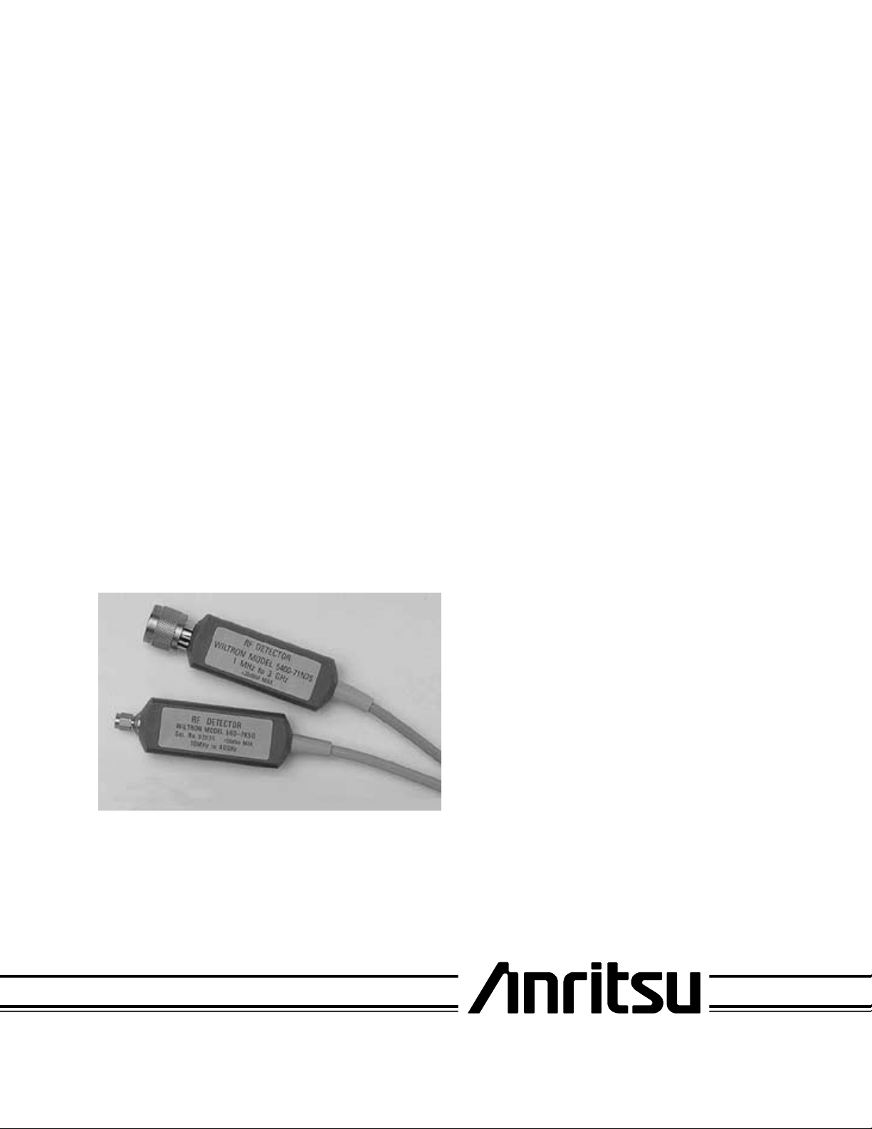
This manual provides descriptions and specifica
tions for ANRITSU Series 560-7XXX and
5400-71XXX RF Detectors (Figure 1). It also con
tains procedures for field replacement of detector di
odes in the model 5400-71B50 and 5400-71B75 RF
detectors andmostof the Series 560-7XXX RF detec
tors.
2. GENERAL DESCRIPTION
The ANRITSU Series 560-7XXX and 5400-71XXX
RF Detectors use zero-biased Schottky diodes and
have a measurement range of –55 dBm to +16 dBm.
The detectors are used with the Model 56100A and
562 Scalar Network Analyzers and with Series
541XXA, 540XXA, and 54XXA Scalar Measurement
Systems for making coaxial transmission loss or
gain and power measurements. The detectors are
also used with the Site Master and Cable Mate Series Personal SWR/RL and Fault Location Testers
for making power measurements.
NOTE: ANRITSU was for
merly known as WILTRON
Figure 1. Typical Series 560-7XXX and 5400-71XXX
RF Detectors
-
3. PERFORMANCE SPECIFICATIONS
Performance specifications for the Series 560-7XXX
and 5400-71XXX RF Detectors are listed in Table 1
on page 2.
-
-
4. PRECAUTIONS FOR USE OF RF
-
DETECTORS
ANRITSU RF Detectors are high-quality, precision
laboratory instruments and should receive the same
care and respect afforded such instruments. Follow
the precautions listed below when handling or con
necting these devices. Complying with these precau
tions will guarantee longer component life and less
equipment downtime due to connector or device fail
ure. Also, such compliance will ensure that RF De
tector failures are not due to misuse or abuse—two
failure modes not covered under the ANRITSU warranty.
a. Beware of Destructive Pin Depth of Mating
Connectors. Based on RF components re-
turned for repair, destructive pin depth of mating connectors is the major cause of failure in
the field. When an RF component connector is
mated with a connector having a destructive pin
depth, damage will usually occur to the RF component connector. A destructive pin depth is one
that is too long in respect ot the reference plane
of the connector (Figure 2, page 3).
The center pin of a precision RF component con
nector has a precision tolerance measured in
mils (1/1000 inch). The mating connectors of
various RF components may not be precision
types. Consequently, the center pins of these de
vices may not have the proper depth. The pin
depth of DUT connectors should be measured to
assure compatibility before attempting to mate
them with RF Detector connectors. An
ANRITSU Pin Depth Gauge (Figure 3, page 3),
or equivalent, can be used for this purpose.
-
-
-
-
-
-
490 JARVIS DRIVE
NOTE: ANRITSU Company was formerly known as WILTRON Company.
l MORGAN HILL, CA 95037-2809
P/N: 10100-00035
REVISION : C
PRINTED: MARCH 2000
COPYRIGHT 1997 ANRITSU CO.
Page 2
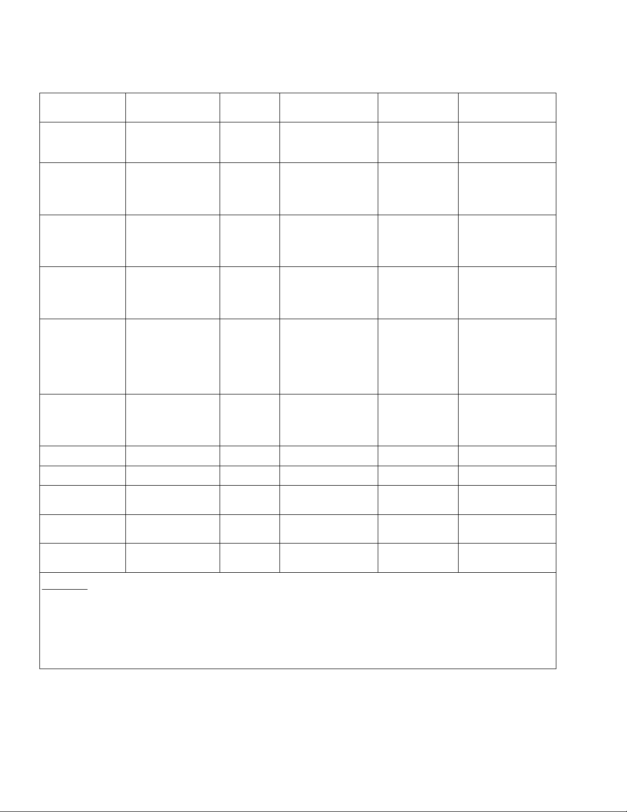
Table 1. 560-7XXX and 5400-71XXX RF Detectors Performance Specifications
Model Frequency Range Impedance Return Loss Input Connector
15 dB, <0.04 GHz
560-7A50 0.01 to 18 GHz
560-7N50B 0.01 to 20 GHz
560-7S50B 0.01 to 20 GHz
560-7S50-2 0.01 to 26.5 GHz
560-7K50 0.01 to 40 GHz
50Ω
50Ω
50Ω
50Ω
50Ω
22 dB, <8 GHz
17 dB, <18 GHz
15 dB, <0.04 GHz
22 dB, <8 GHz
17 dB, <18 GHz
14 dB, <20 GHz
15 dB, <0.04 GHz
22 dB, <8 GHz
17 dB, <18 GHz
14 dB, <20 GHz
15 dB, <0.04 GHz
22 dB, <8 GHz
17 dB, <18 GHz
14 dB, <26.5 GHz
12 dB, <0.04 GHz
22 dB, <8 GHz
17 dB, <18 GHz
15 dB, <26.5 GHz
14 dB, <32 GHz
13 dB, <40 GHz
GPC-7
N(m)
WSMA(m)
WSMA(m)
K(m)
Frequency
Response
±0.5 dB, 18 GHz
±0.5 dB, <18 GHz
±1.25 dB, <20 GHz
±0.5 dB, <18 GHz
±1.25 dB, <20 GHz
±0.5 dB, <18 GHz
±1.25 dB, <26.5 GHz
±0.5 dB, <18 GHz
±1.25 dB, <26.5 GHz
±2.2 dB, <32 GHz
±2.5 dB, <40 GHz
12 dB, <0.04 GHz
560-7VA50 0.01 to 50 GHz
5400-71B50 0.001 to 1.5 GHz
5400-71B75 0.001 to 1.5 GHz
5400-7N50 0.001 to 3 GHz
5400-71N75 0.001 to 3 GHz
5400-71N75L* 0.005 to 1.2 GHz
All Models
Maximum Input Power: 100mW (+20 dBm)
Cable Length: 122 cm (4 ft)
Dimensions: 7.6 x 2.9 x 2.2 cm (3 x 1-1/8 x 7/8 in.)
Weight: 170g (6 oz)
* The input of the 5400-71N75L is limited to extend the damage level to 1W (+30 dBm)
The limit begins compression at 10 dBm <0.05 GHz, 15 dBm <1 GHz, or 20 dBm <1.2 GHz
:
50Ω
50Ω
75Ω
50Ω
75Ω
75Ω
19 dB, <20 GHz
15 dB, <40 GHz
10 dB, <50 GHz
20dB BNC(m)
20 dB BNC(m)
26 dB N(m)
26 dB, <2 GHz
20 dB, <3 GHz
24 dB N(m)
V(m)
N(m)
±0.8 dB, <20 GHz
±2.5 dB, <40 GHz
±3.0 dB, <50 GHz
±0.2 dB, <1.5 GHz
±0.2 dB, <1.5 GHz
±0.2 dB, <1 GHz
±0.3 dB, <3 GHz
±0.2 dB, <1 GHz
±0.3 dB, <3 GHz
±0.2 dB, <1 GHz
±0.5 dB, <1.2 GHz
2 DET OMM
Page 3
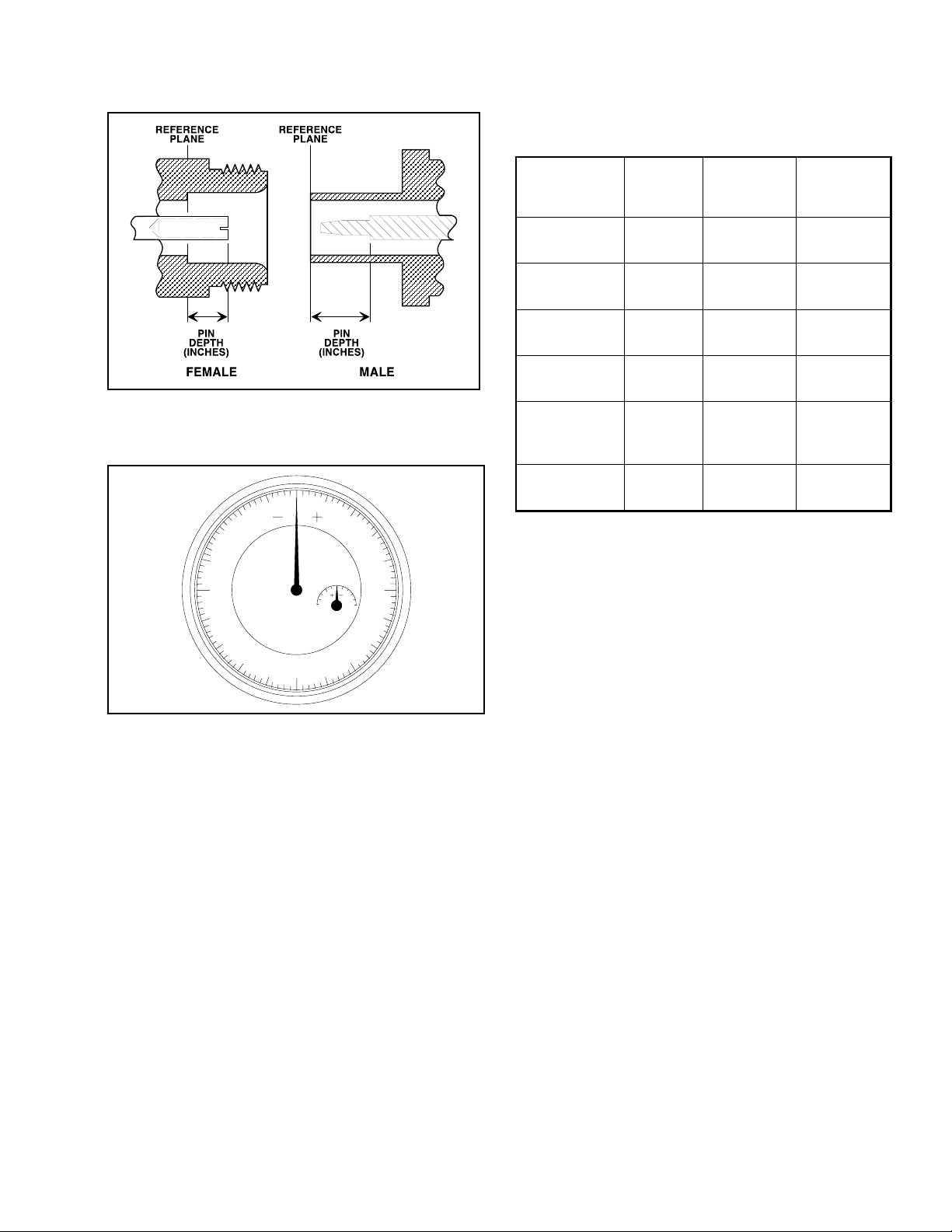
Table 2. Allowable Device Under Test (DUT)
Connector Pin Depth
Figure 2. N Connector Pin Depth Definition
0
1
2
3
4
1
11
2
4
2
2
3
5
Figure 3. Pin Depth Gauge
DUT
Connector
Type
N-Male
N-Female
GPC-7
WSMA-Male
WSMA-Female
SMA-Male,
SMA-Female
3.5 mm-Male
3.5
mm-Female
K-Male,
K-Female
ANRITSU
Gauging
Set Model
01-163
01-161
01-162
01-162
01-162
01-162
Pin Depth
(inches)
.207–0.000
+
0.030
+
0.000
–
0.030
–
0.000
–
0.010
–
0.000
–
0.010
–
0.000
–
0.010
+
0.000
–
0.010
Pin Depth
Gauge
Reading
207 +0.000
–
0.030
Same as
Pin Depth
Same as
Pin Depth
Same as
Pin Depth
Same as
Pin Depth
Same as
Pin Depth
handling. However, do not drop or otherwise
treat them roughly. Mechanical shock will significantly reduce their service life.
d. Avoid Applying Excessive Power. The Se-
ries 560-7XXX and 5400-71XXX RF Detectors
are rated at +20 dBm (100 mW) maximum input
power. Exceeding this input power level, even
for short durations, will permanently damage
their internal components.
If the measured connector is out of tolerance in
the “+” region, the center pin is too long (see Ta
ble 2). Mating under this condition will likely
damage the precision RF Detector connector. If
the test device connector measures out of toler
ance in the “–” region, the center pin is too short.
This will not cause damage, but it will result in a
poor connection and a consequent degradation
in performance.
b. Avoid Over Torquing Connectors. Over
torquing connectors is destructive; it may dam
age the connector center pin. Finger-tightis usu
ally sufficient for Type N connectors. Always use
a connector torque wrench (8 inch-pounds) when
tightening GPC-7, WSMA, K, or V type connec
tors. Never use pliers to tighten connectors.
c. Avoid Mechanical Shock. RF Detectors are
designed to withstand years of normal bench
e. Do Not Disturb Teflon Tuning Washers on
-
Connector Center Pins. The center conduc
tor of many RF component connectors contains a
small teflon tuning washer that is located near
-
the point of mating (Figure 4, page 4). This
washer compensates for minor impedance dis
continuities at the interface. Do not disturb this
washer. The location of this washer is critcal to
the performance of the RF component.
f. Keep Connectors Clean. The precise geome
-
-
try that makes possible the RF component’s high
performance can be easily disturbed by dirt or
other contamination adhering to connector in
terfaces. When not in use, keep the connectors
-
covered.
To clean the connector interfaces, use a clean
cotton swab that has been dampened with dena
tured alcohol. Figure 5, page 4 illustrates the
cleaning of male and female connectors.
DET OMM 3
-
-
-
-
-
Page 4
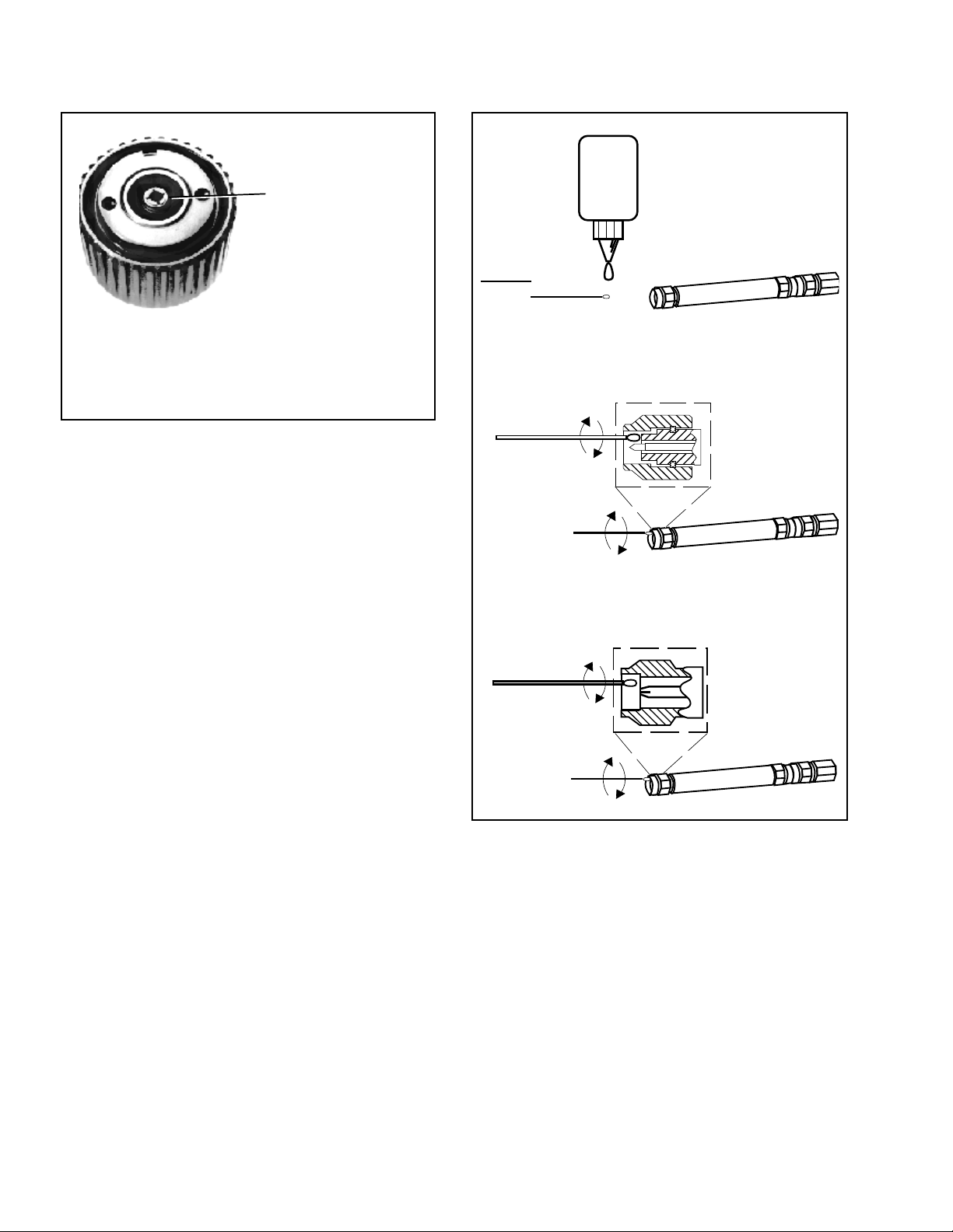
Figure 4. Tuning Washer on GPC-7 Connector
DENATURED
ALCOHOL
DAMPEN ONLY
DO NOT
SATURATE
MALE
FEMALE
TEFLON WASHER
NOTE
The teflon washer is shown on a GPC-7
connector. A similar washer may be installed
on any ANRITSU precision connector.
NOTE
Most cotton swabs are too large to fit
in the smaller connector types. In
these cases it is necessary to peel off
most of the cotton and then twist the
remaining cotton tight. Be sure that
the remaining cotton does not get
stuck in the connector. Cotton swabs
of the appropriate size can be purchased through a medical-laboratory-type supply center.
The following are some important tips on cleaning connectors:
•
Use only denatured alcohol as a cleaning sol
vent.
•
Do not use excessive amounts of alcohol as
prolonged drying of the connector may be re
quired.
•
Never put lateral pressure on the center pin
of the connector.
•
If installed, do not disturb the teflon washer
on the center conductor pin.
•
Verify that no cotton or other foreign mate
rial remains in the connector after cleaning
it.
•
If available, use compressed air to remove
foreign particles and to dry the connector.
•
After cleaning, verify that the center pin has
not been bent or damaged.
-
-
Figure 5. Cleaning Male and Female Connectors
5. DETECTOR DIODE REPLACEMENT
RF Detector models 5400-71B50 and 5400-71B75
are equipped with field-replaceable detector diodes;
-
the series 560-7XXX RF Detectors, except for model
560-7VA50, are equipped with field-replaceable de
tector diode modules. Paragraph 5.1 provides a pro
cedure for replacing defective diodes in the models
5400-71B50 and 5400-71B75; paragraph 5.2 pro
vides a procedure for replacing detector diode mod
ules in series 560-7XXX RF Detectors.
-
-
-
-
4 DET OMM
Page 5

Table 3 provides the diode/diode module part num
DIODE
CATHODE END
R1
R4
1
342
ber for each RF detector model containing a
field-replaceable detector diode or diode module.
Table 3. 560-7XXX and 5400-71XXX RF Detector
Diode/Diode Module Part Numbers
RF Detector Model
5400-71B50 10-21
5400-71B75 10-88
Diode or Diode
Module Part Number
-
fective diode is removed, but before the replace
ment diode is installed.
b. Test Equipment Required The detector di
ode replacement procedures require a digital
multimeter (DMM) that has a display resolution
of at least 3-1/2 digits (John Fluke Model 8840A,
or equivalent).
5.1. Detector Diode Replacement for the
Model 5400-71B50 and 5400-71B75 RF
Detectors
-
-
5400-71N50 Factory Replacement Only
5400-71N75 Factory Replacement Only
560-7A50 A7219A
560-7N50B C24441
560-7S50B C24441
560-7S50-2 A7219B
560-7K50 ND19393
560-7VA50 Factory Replacement Only
NOTE
RF Detector Models 5400-71N50,
5400-71N75, and 560-7VA50 do not have
field-replaceable detector diodes. Contact
your local ANRITSU Service Center for
assistance.
a. Required Adjustments Whenever the detec
tor diode (or diode module) of the RF detector is
replaced, the two potentiometers that are part of
the RF detector PCB subassembly (Figures 6
(below) and 9 (page 6)) must be readjusted. The
potentiometer readjustment is done after the de
The model 5400-71B50 and 5400-71B75 RF Detec
tors are equipped with a field-replaceable detector
diode. To replace, proceed as follows:
1. Unfasten the four detector housing top cover
retaining screws. Remove the top cover.
2. Unplug the defective diode (Figure 6) from
the PCB subassembly and remove.
3. Set the potentiometer R1 full clockwise (max
imum resistance).
4. Connect the DMM leads between pins 1 and 2
of the RF detector cable connector (Figure 7).
Measure the resistance value, which is the
maximum resistance of R1 (approximately
40.5 KΩ is typical). Record this value; it will
hereafter be referred to as “R
”.
T
-
Figure 7. RF Detector Cable Connector Pin Layout
-
-
-
5. Obtain the “K” value from the replacement di
-
ode container level (Figure 8, page 6).
6. Compute the set value for R1 as follows:
RKR
1 =×
set T
7. Adjust R1 counterclockwise until the DMM
indicates the R1
value calculated in step 6.
set
8. Connect the DMM leads between pin 3 of the
Figure 6. Model 5400-71B50 and 5400-71B75
RF Detectors Housing Layout Diagram
DET OMM 5
RF detector cable connector and the cable
shield.
9. Obtain the “R
” value from the replacement
O
diode container label (Figure 8, page 6).
Page 6

ANRITSU
RETAINING SCREWS (4)
LABEL
TOP COVER
CABLE RETAINER
A1 PCB
R1
DETECTOR
HOUSING
WSMA OR
K CONNECTOR
GPC-7
CONNECTOR
TYPE N
CONNECTOR
*
THE DETECTOR MAY OR MAY NOT INCLUDE THIS SHIM.
THE SHIM IS ADDED DURING MANUFACTURE AS NEEDED.
MODULE LEAD
RECEPTACLES (3)
R4
*SHIM
DIODE MODULE
MODULE RETAINER
10 - 88
DETECTOR DIODE
K______________
R _____________
0
Figure 8. Replacement Diode Container Label
10. Adjust R4 until the DMM indicates the “RO”
value. Disconnect the DMM.
11. Orient the cathode end (white dot) of the re
placement diode as shown in Figure 6 (white
dot towards centerline of the detector PCB
subassembly). Insert the diode into the socket
of the PCB subassembly.
12. Reinstall the top cover, securing it with the
four retaining screws. This completes replace
ment of the detector diode.
5.2. Detector Diode Module Replacement
for the Series 560-7XXX RF Detectors
Series 560-7XXX RF Detectors, except for model
560-7VA50, are equipped with a field-replaceable di
ode module that contains (in addition to the detector
diode) a thermistor, a resistor, and two capacitors.
To replace, proceed as follows:
1. Unfasten the four detector housing top cover
-
retaining screws. Remove the top cover.
2. Unfasten the two retaining screws that hold
down the RF detector PCB subassembly (Fig
ure 9).
-
-
-
Figure 9. Series 560-7XXX RF Detectors, Exploded View
6 DET OMM
Page 7

3. Slide the cable retainer out ofthe RF detector
1
342
housing assembly. When the cable retainer
clears the housing, disconnect the PCB subas
sembly from the diode module. Remove the
spring washer.
4. Remove the fiberglass module retainer from
the detector housing. This retainer can be re
moved by prying it out using a small screw
driver, or by pulling it out using short, round
nose pliers.
5. Remove the diode module from the rear of the
connector body by pulling it straight out.
6. Connect the DMM leads between pins 1 and 2
of the RF detector cable connector (Figure 10).
Measure the resistance value, which is the
maximum resistance of R1 (approximately
40.5 KΩ is typical). Record this value; it will
hereafter be referred to as “R
”.
T
8. Compute the set value for R1 as follows:
1 =×
RKR
-
9. Adjust R1 counerclockwise until the DMM in
dicates the R1
set T
set
-
value calculated in step 8.
10. Connect the DMM leads between pin 3 of the
-
-
RF detector cable connector and the cable
shield.
11. Obtain the “R
” value from the replacement
0
diode container label and adjust R4 until the
DMM indicates this value. Disconnect the
DMM.
12. Orient the detector housing normally (Figure
9, page 6). Insert the replacement diode mod
ule into the rear of the connector body so that
the center lead is on top.
13. Orient the spring washer so that the two
curved flanges point toward the rear of the
detector housing and are positioned horizon
-
tally (i.e., 3 o’clock and 9o’clock positions).
14. Insert fiberglass module retainer between the
replacement diode module and the spring
washer. push down on the retainer until fully
seated.
Figure 10. RF Detector Cable Connector Pin Layout
7. Obtain the “K” value from the replacement di
ode container label (Figure 11).
ANRITSU
A7219A
DETECTOR DIODE
K______________
_____________
R
0
Figure 11. Replacement Diode Module Container Label
15. Orient the PCB subassembly normally as
shown in Figure 9 andinsert it into the detector housing so that the leads from the replacement diode module mate with the connectors
on the PCB subassembly.
-
16. Insert the cable retainer into the slot in the
detector housing.
17. Fasten the PCB subassembly into the detec
tor housing using two retaining screws.
18. Reinstall the top cover, securing it with four
retaining screws. This completes replacement
of the detector diode module.
6. ANRITSU Service Centers
Table 4, page 8, provides names and addresses of
ANRITSU Service Centers.
-
DET OMM 7
Page 8

Table 4. ANRITSU Service Centers
UNITED STATES
ANRITSU COMPANY
685 Jarvis Drive
Morgan Hill, CA 95037-2809
Telephone: (408) 776-8300
FAX: 408-776-1744
COMPANY
10 Kingsbridge Road
Fairfield, NJ 07004
Telephone: (201) 227-8999
FAX: 201-575-0092
AUSTRALIA
ANRITSU PTY. LTD.
Unit 3, 170 Foster Road
Mt Waverley, VIC 3149
Australia
Telephone: 03-9558-8177
Fax: 03-9558-8255
BRAZIL
ANRITSU ELECTRONICA LTDA.
Praia de Botafogo, 440, Sala 2401
CEP22250-040, Rio de Janeiro, RJ, Brasil
Telephone: 021-28-69-141
Fax: 021-53-71-456
CANADA
ANRITSU INSTRUMENTS LTD.
215 Stafford Road, Unit 102
Nepean, Ontario K2H 9C1
Telephone: (613) 828-4090
FAX: (613) 828-5400
CHINA
BEIJING SERVICE
CENTER
Beijing Fortune Building
416W, 5 Dong San Huan Bei Lu
Chaoyang qu
Beijing 100004, China
Telephone: 011861065909237
FAX: 011861065909236
FRANCE
ANRITSU S.A
9 Avenue du Quebec
Zone de Courtaboeuf
91951 Les Ulis Cedex
Telephone: 016-44-66-546
FAX: 016-44-61-065
GERMANY
ANRITSU GmbH
Grafenberger Allee 54-56
D-40237 Dusseldorf
Germany
Telephone: 0211-968550
FAX: 0211-9685555
INDIA
MEERA AGENCIES (P) LTD.
A-23 Hauz Khas
New Delhi 110 016
Telephone: 011-685-3959
FAX: 011-686-6720
ISRAEL
TECH-CENT, LTD
Haarad St. No. 7, Ramat Haahayal
Tel-Aviv 69701
Telephone: (03) 64-78-563
FAX: (03) 64-78-334
ITALY
ANRITSU Sp.A
Roma Office
Via E. Vittorini, 129
00144 Roma EUR
Telephone: (06) 50-22-666
FAX: (06) 50-22-4252
JAPAN
ANRITSU CORPORATION
1800 Onna Atsugi-shi
Kanagawa-Prf. 243 Japan
Telephone: 0462-23-1111
FAX: 0462-25-8379
KOREA
ANRITSU KOREA (AWK)
#901 Daeo Bldg. 26-5
Yeoido Dong, Youngdeungpo
Seoul Korea 150 010
Telephone: 02-782-7156
FAX: 02-782-4590
SINGAPORE
ANRITSU (SINGAPORE) PTE LTD
3 Shenton Way #24-03
Shenton House
Singapore 0106
Telephone: 2265206
FAX: 2265207
SOUTH AFRICA
ETESCSA
1st Floor Montrose Place
Waterfall Park
Becker Road
MIDRAND
SOUTH AFRICA
Telephone: 011-315-1366
Fax: 011-315-2175
SWEDEN
ANRITSU AB
Botvid Center
S-14584
Stockholm, Sweden
Telephone: (08) 534-717-00
FAX: (08) 534-717-30
TAIWAN
CO., LTD.
8F, No. 96, Section 3
Chien Kuo N. Road
Taipei, Taiwan, R.O.C.
Telephone: (02) 515-6050
FAX: (02) 509-5519
UNITED KINGDOM
ANRITSU LTD.
200 Capability Green
Luton, Bedfordshire
LU1 3LU, England
Telephone: 015-82-41-88-53
FAX: 015-82-31-303
8 DET OMM
Page 9

NOTES
DET OMM 9
Page 10

NOTES
10 DET OMM
Page 11

WARRANTY
The ANRITSU product(s) listed on the title page is (are) warranted against defects in ma
terials and workmanship for one year from the date of shipment.
ANRITSU’s obligation covers repairing or replacing products which prove to be defective
during the warranty period. Buyers shall prepay transportation charges for equipment
returned to ANRITSU for warranty repairs. Obligation is limited to the original pur
chaser. ANRITSU is not liable for consequential damages.
LIMITATION OF WARRANTY
The foregoing warranty does not apply to ANRITSU connectors that have failed due to
normal wear. Also, the warranty does not apply to defects resulting from improper or inadequate maintenance by the Buyer, unauthorized modification or misuse, or operation
outside of the environmental specifications of the product. No other warranty is expressed or implied, and the remedies provided herein are the Buyer’s sole and exclusive
remedies.
TRADEMARK ACKNOWLEDGEMENTS
V Connector and K Connector are registered trademarks of ANRITSU Company.
NOTICE
ANRITSU Company has prepared this manual for use by ANRITSU Company personnel
and customers as a guide for the proper installation, operation and maintenance of
ANRITSU Company equipment and computer programs. The drawings, specifications,
and information contained herein are the property of ANRITSU Company, and any unautho
rized use or disclosure of these drawings, specifications, and information is prohibited; they
shall not be reproduced, copied, or used in whole or in part as the basis for manufacture or
sale of the equipment or software programs without the prior written consent of ANRITSU
Company.
-
-
-
Page 12

 Loading...