Anritsu HFE1103 Stauffer

22 High Frequency Electronics
High Frequency Design
VARACTOR MODEL
Finding the Lumped Element
Varactor Diode Model
By George H. Stauffer
Rockwell Collins
A
n accurate model
for the varactor
diode is necessary
when designing a voltage
controlled oscillator
(VCO) using CAD simulation. In order to predict
tuning range, start up
gain, and phase noise, the
resonator must be accu-
rately modeled over the frequency range of the
oscillations. The varactor diode used for tuning has a predominant effect on the Q, phase
noise and tuning range of the resonator. If the
varactor model is inaccurate, the results of the
most elaborate computer simulation will be
misleading and the oscillator, when built, may
have disappointing performance.
Varactor Diode Model
Figure 1 shows a commonly used lumped
element varactor diode model. The values for
package inductance and capacitance, L
p
and
C
p
shown are typical for an 0805 surface
mount part. The values for junction capacitance, C
j
and Q are supplied by the manufacturer and are almost always specified at a low
frequency, usually 50 MHz, and a bias voltage
of –4 Volts. Q is defined by Q = 1/ωC
jRs
. This
formula can be used to calculate the series
resistance R
s
of the varactor model at the
measured frequency, however at microwave
frequencies additional losses often result in a
significantly higher value for R
s
. Also, R
s
decreases with increasing bias voltage as the
width of the depletion region around the PN
junction increases, reducing the length of the
conductive path through the bulk semiconductor material surrounding the junction.
R
s
is sometimes assumed to be constant
with reverse voltage and frequency in order to
simplify use of the model. A much more accurate picture can be had by measuring the
diode close to operating conditions and then
choosing values for the lumped element model
based on these measurements. Two important
operating conditions are the frequency at
which the diode is to be used and mounting
method. One way would be to simply mount
the diode at the end of a 50 ohm transmission
line and measure S
11
of the two-terminal
diode using a network analyzer. However,
unless extreme care is taken to make a very
accurate S
11
calibration at the point where the
diode is mounted, the calculated real part of
the diode impedance, R
s
may have a large
error because the impedance of the diode is
close to the edge of the Smith chart. A more
accurate network analyzer measurement is
made by first matching the diode to 50 ohms
Here is a method for
using measured data to
accurately describe the
behavior of a varactor
diode, providing the CAD
simulator with a model that
corresponds to actual
device performance
Figure 1 · Lumped element model of varactor diode using manufacturer’s specifications.
R
s
is calculated from Q= 1/
ωω
CjR
s
at 50
MHz.
From November 2003 High Frequency Electronics
Copyright © 2003 Summit Technical Media, LLC

24 High Frequency Electronics
High Frequency Design
VARACTOR MODEL
at the frequency of interest. A matching structure which uses only
microstrip elements is preferable
because it can be analyzed quite
accurately using an EM simulator
and its effect in the circuit can then
be accounted for when calculating the
model parameters.
An Accurate Model is Required
for VCO Design
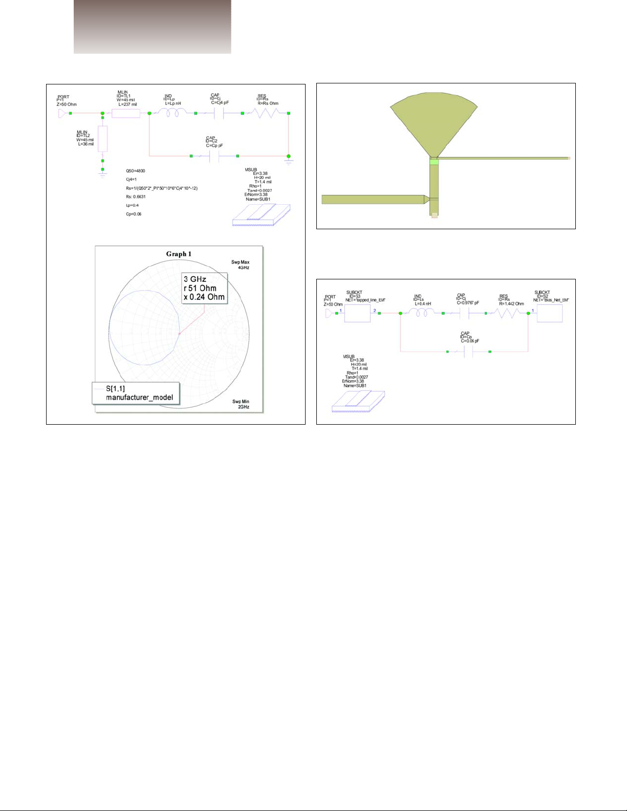
A recent 3 GHz VCO design
required that the resonator circuit be
optimized for best phase noise and
tuning range, yet also allow for adequate production margin. A suitable
varactor diode was selected based on
the required range of capacitance
variation. In order to begin to accurately characterize the diode, the
model with values supplied by the
manufacturer was matched at 3 GHz
using a microstrip network as shown
in Figure 2a. The swept frequency
response from 2 to 4 GHz describes a
loop on the Smith chart as shown in
Figure 2b. At 3 GHz the resonance
loop passes through the center of the
Smith chart indicating critical coupling.
From this point it is a simple matter to add microstrip elements to produce a practical circuit to be used as
a test fixture. The layout is shown in
Figure 3 and includes a biasing network consisting of a radial stub and a
high impedance quarter wave line. At
3 GHz the bias network is an RF
short at the cathode terminal.
The S-parameters of the bias network and the tapped line are calculated individually using an EM simulation program and the results are
used in the measurement fixture
schematic in Figure 4.
This layout was reproduced on 20
mil Rogers 4003 board, and this 2 x 2
inch board was mounted on a test fixture block, shown in Figure 5. The
network analyzer was calibrated at
the coax connector, with the reference
plane brought to the edge of the
board using a 16.7 ps port extension.
The S
11
measurements were then
made at bias voltages over a 0-20 V
range while sweeping from 2 to 4
GHz.
The S
11
measurements were
saved and imported into the CAD
program. After these measurements,
all that remains to be done is to
adjust C
j
and Rsof the model of
Figure 4 so that the measured S
11
agrees with S11calculated from
Figure 4 over the entire 2 to 4 GHz
frequency range for each value of bias
Figure 3 · Microstrip test fixture with tapped line and
bias circuit.
Figure 2 · Varactor diode model matched to 50 ohms
using microstrip tapped line (a); S
11
from 2 to 4 GHz (b).
Figure 4 · Tapped line and bias network models from EM
simulation connected to diode model.
(a)
(b)
 Loading...