


SERIES 682XXB/683XXB
SYNTHESIZED SIGNAL GENERATORS
MAINTENANCE MANUAL
490 JARVIS DRIVE
MORGAN HILL, CA 95037-2809
P/N: 10370-10290 REVISION: H PRINTED: AUGUST 2003
COPYRIGHT 2003 ANRITSU CO.

WARRANTY
The ANRITSU product(s) listed on the title page is (are) warranted against defects in materials and workmanship for one year from the date of shipment.
ANRITSU’s obligation covers repairing or replacing products which prove to be defective during the warranty period. Buyers shall prepay transportation charges for equipment returned to ANRITSU for warranty repairs. Obligation is limited to the original purchaser. ANRITSU is not liable for consequential damages.
LIMITATION OF WARRANTY
The foregoing warranty does not apply to ANRITSU connectors that have failed due to normal wear. Also, the warranty does not apply to defects resulting from improper or inadequate maintenance by the Buyer, unauthorized modification or misuse, or operation outside of the environmental specifications of the product. No other warranty is expressed or implied, and the remedies provided herein are the Buyer’s sole and exclusive remedies.
TRADEMARK ACKNOWLEDGEMENTS
Adobe Acrobat is a registered trademark of Adobe Systems Incorporated.
NOTICE
ANRITSU Company has prepared this manual for use by ANRITSU Company personnel and customers as a guide for the proper installation, operation, and maintenance of ANRITSU Company equipment and computor programs. The drawings, specifications, and information contained herein are the property of ANRITSU Company, and any unauthorized use or disclosure of these drawings, specifications, and information is prohibited; they shall not be reproduced, copied, or used in whole or in part as the basis for manufacture or sale of the equipment or software programs without the prior writtten consent of ANRITSU Company.


Table Of Contents
Chapter 1 - General Information
1-1 |
SCOPE OF MANUAL . . . . . . . . . . . . . . . . . 1-3 |
|||
1-2 |
INTRODUCTION . . . . . . . . . . . . . . . . . . . 1-3 |
|||
1-3 |
DESCRIPTION . . . . . . . . . . . . . . . . . . . . 1-3 |
|||
1-4 |
IDENTIFICATION NUMBER . . . . . . . . . . . . 1-5 |
|||
1-5 |
ELECTRONIC MANUAL . . . . . . . . . . . . . . . 1-6 |
|||
1-6 |
RELATED MANUALS . . . . . . . . . . . . . . . . 1-6 |
|||
|
Operation Manual . . . . . . . . . . . . . . . . 1-6 |
|||
|
GPIB Programming Manual . . . . . . . . . . . 1-6 |
|||
|
SCPI Programming Manual . . . . . . . . . . . 1-6 |
|||
1-7 |
OPTIONS . . . . . . . . . . . . . . . . . . . . . . . 1-7 |
|||
1-8 |
LEVEL OF MAINTENANCE . . . . . . . . . . . . . 1-8 |
|||
|
Troubleshooting |
. . . . . . . . . . . . . . . . |
. 1-8 |
|
|
Repair . . . |
. . |
. . . . . . . . . . . . . . . . |
. 1-8 |
|
Calibration |
. . . . . . . . . . . . . . . . . . . 1-8 |
||
|
Preventive Maintenance . . . . . . . . . . . . . 1-8 |
|||
1-9 |
PREVENTIVE MAINTENANCE . . . . . . . . . . . 1-9 |
|||
1-10 |
STATIC-SENSITIVE COMPONENT HANDLING |
|
||
|
PRECAUTIONS . . . . . . . . . . . . . . . . . . . 1-9 |
|||
1-11 |
STARTUP CONFIGURATIONS. . . . . . . . . . . 1-11 |
|||
1-12 |
RECOMMENDED TEST EQUIPMENT . . . . . . 1-12 |
|||
1-13 |
EXCHANGE ASSEMBLY PROGRAM . . . . . . . 1-14 |
|||
1-14 |
REPLACEABLE SUBASSEMBLIES AND PARTS 1-14 |
|||
Chapter 2 - Functional Description
2-1 |
INTRODUCTION . . . . . . . . . . . . . . . . . . . 2-3 |
||
2-2 |
682XXB/683XXB MAJOR SUBSYSTEMS . . . . . . 2-3 |
||
|
Digital Control. . . . . . . . . . . . . . . . . . 2-3 |
||
|
Front Panel . . . . . . . . . . . . . . . . . . . 2-4 |
||
|
Frequency Synthesis . . . . . . . . . . . . . . . 2-4 |
||
|
Analog Instruction . . . . . . . . . . . . . . . . 2-5 |
||
|
YIG Driver . . . . |
. . . . . . |
. . . . . . . . . 2-5 |
|
Function Generator |
. . . . . . |
. . . . . . . . . 2-5 |
682XXB/683XXB MM |
i |

Table of Contents (Continued)
|
ALC/AM/Pulse Modulation . . . . . . . . . . . . 2-8 |
|
|
RF Deck . . . . . . . . . . . . . . . . . . . . . 2-8 |
|
|
Power Supply . . . . . . . . . . . . . . . . . . 2-8 |
|
|
Inputs/Outputs . . . . . . . . . . . . . . . . |
. 2-8 |
|
Motherboard/Interconnections . . . . . . . . . . 2-9 |
|
2-3 |
FREQUENCY SYNTHESIS . . . . . . . . . . . . . 2-9 |
|
|
Phase-Lock Loops . . . . . . . . . . . . . . . . 2-9 |
|
|
Overall Operation . . . . . . . . . . . . . . . |
2-10 |
|
RF Outputs 0.01 to 65 GHz . . . . . . . . . . . |
2-13 |
|
Frequency Modulation . . . . . . . . . . . . . 2-14 |
|
|
Phase Modulation (Option 6) . . . . . . . . . . 2-14 |
|
|
Analog Sweep Mode (683XXB only) . . . . . . . |
2-14 |
|
Step Sweep Mode. . . . . . . . . . . . . . . . |
2-15 |
2-4 |
ALC/AM/PULSE MODULATION . . . . . . . . . . |
2-15 |
|
ALC Loop Operation . . . . . . . . . . . . . . 2-15 |
|
|
Pulse Generator Operation . . . . . . . . . . . |
2-18 |
2-5 |
RF DECK ASSEMBLIES . . . . . . . . . . . . . . |
2-19 |
|
RF Deck Configurations . . . . . . . . . . . . |
2-20 |
|
YIG-tuned Oscillator . . . . . . . . . . . . . . 2-20 |
|
|
Power Level Control and Modulation . . . . . . |
2-23 |
|
RF Signal Filtering . . . . . . . . . . . . . . . 2-23 |
|
|
0.01 to 2 GHz Down Converter . . . . . . . . . |
2-24 |
|
0.5 to 2.2 GHz Digital Down Converter . . . . . |
2-25 |
|
Switched Doubler Module. . . . . . . . . . . . 2-26 |
|
|
Source Quadrupler Module . . . . . . . . . . . 2-29 |
|
|
Power Level Detection/ALC Loop . . . . . . . . 2-30 |
|
|
Step Attenuator . . . . . . . . . . . . . . . . |
2-31 |
Chapter 3 - Performance Verification
3-1 |
INTRODUCTION . . . . . . . . . . . . . . . . . . . 3-3 |
3-2 |
RECOMMENDED TEST EQUIPMENT . . . . . . . 3-3 |
3-3 |
TEST RECORDS . . . . . . . . . . . . . . . . . . . 3-3 |
3-4 |
CONNECTOR AND KEY LABEL NOTATION . . . 3-3 |
3-5 |
682XXB/683XXB POWER LEVELS . . . . . . . . . 3-6 |
3-6 |
INTERNAL TIME BASE AGING RATE TEST . . . 3-8 |
|
Test Setup . . . . . . . . . . . . . . . . . . . . 3-8 |
|
Test Procedure. . . . . . . . . . . . . . . . . . 3-9 |
ii |
682XXB/683XXB MM |

Table of Contents (Continued)
3-7 |
FREQUENCY SYNTHESIS TESTS . . . . . . . . 3-11 |
|
|
Test Setup . . . . . . . . . . . . . . . . . . . 3-11 |
|
|
Coarse Loop/YIG Loop Test Procedure. . . . . . |
3-12 |
|
Fine Loop Test Procedure . . . . . . . . . . . . 3-13 |
|
3-8 |
SPURIOUS SIGNALS TEST: RF OUTPUT SIGNALS |
|
|
2 GHz ( 2.2 GHz for 68XX5B MODELS). . . . . |
3-14 |
|
Test Setup . . . . . . . . . . . . . . . . . . . 3-14 |
|
|
0.01 - 2 GHz Test Procedure . . . . . . . . . . |
3-14 |
|
0.5 - 2.2 GHz Test Procedure . . . . . . . . . . 3-17 |
|
3-9 |
HARMONIC TEST: RF OUTPUT SIGNALS |
|
|
FROM 2 TO 20 GHz . . . . . . . . . . . . . . . . |
3-18 |
|
Test Setup . . . . . . . . . . . . . . . . . . . 3-18 |
|
|
Test Procedure (2 to 10 GHz) . . . . . . . . . . |
3-19 |
|
Test Procedure (11 to 20 GHz) . . . . . . . . . |
3-20 |
3-10 |
SINGLE SIDEBAND PHASE NOISE TEST . . . . 3-22 |
|
|
Test Setup . . . . . . . . . . . . . . . . . . . 3-22 |
|
|
Test Procedure . . . . . . . . . . . . . . . . . 3-23 |
|
3-11 |
POWER LEVEL ACCURACY AND FLATNESS |
|
|
TESTS. . . . . . . . . . . . . . . . . . . . . . . . |
3-26 |
|
Test Setup . . . . . . . . . . . . . . . . . . . 3-26 |
|
|
Power Level Accuracy Test Procedure . . . . . . |
3-27 |
|
Power Level Flatness Test Procedure . . . . . . |
3-27 |
3-12 |
AMPLITUDE MODULATION TEST . . . . . . . . 3-30 |
|
|
Test Setup . . . . . . . . . . . . . . . . . . . 3-30 |
|
|
AM Input Sensitivity Procedure. . . . . . . . . |
3-31 |
3-13 |
FREQUENCY MODULATION TESTS . . . . . . . 3-33 |
|
|
Test Setup . . . . . . . . . . . . . . . . . . . 3-33 |
|
|
FM Input Sensitivity Procedure. . . . . . . . . 3-33 |
|
3-14 |
PULSE MODULATION TESTS: RISE TIME, |
|
|
FALL TIME, OVERSHOOT, AND LEVEL . . . . 3-39 |
|
|
Test Setup . . . . . . . . . . . . . . . . . . . 3-39 |
|
|
Rise/Fall Time and Overshoot. . . . . . . . . . 3-40 |
|
|
Pulse Leveling Accuracy . . . . . . . . . . . . |
3-41 |
3-15 |
PULSE MODULATION TEST: VIDEO |
|
|
FEEDTHROUGH. . . . . . . . . . . . . . . . . . |
3-43 |
|
Test Setup . . . . . . . . . . . . . . . . . . . 3-43 |
|
|
Test Procedure . . . . . . . . . . . . . . . . . |
3-44 |
682XXB/683XXB MM |
iii |

Table of Contents (Continued)
3-16 PULSE MODULATION TEST: RF ON/OFF RATIO 3-45 Test Setup . . . . . . . . . . . . . . . . . . . 3-45 Test Procedure . . . . . . . . . . . . . . . . . 3-45
3-17 PHASE MODULATION TESTS. . . . . . . . . . . 3-48 Test Setup . . . . . . . . . . . . . . . . . . . 3-48M Input Sensitivity Procedure. . . . . . . . . 3-48
Chapter 4 - Calibration
4-1 |
INTRODUCTION . . . . . . . . . . . . . . . . . . . 4-3 |
|
4-2 |
RECOMMENDED TEST EQUIPMENT . . . . . . . 4-3 |
|
4-3 |
TEST RECORDS . . . . . . . . . . . . . . . . . . . |
4-3 |
4-4 |
CALIBRATION FOLLOWING SUBASSEMBLY |
|
|
REPLACEMENT. . . . . . . . . . . . . . . . . . . 4-4 |
|
4-5 |
CONNECTOR AND KEY LABEL NOTATION . . . 4-4 |
|
4-6 |
INITIAL SETUP. . . . . . . . . . . . . . . . . . . . 4-7 |
|
|
Interconnection . . . . . . . . . . . . . . . . . 4-7 |
|
|
PC Setup — Windows 3.1 . . . . . . . . . . . . |
4-8 |
|
PC Setup — Windows 95 . . . . . . . . . . . . |
4-10 |
4-7 |
PRELIMINARY CALIBRATION . . . . . . . . . . |
4-13 |
|
Equipment Setup . . . . . . . . . . . . . . . . 4-13 |
|
|
Calibration Steps . . . . . . . . . . . . . . . . |
4-14 |
4-8 |
SWITCHED FILTER SHAPER CALIBRATION . . 4-17 |
|
|
Equipment Setup . . . . . . . . . . . . . . . . 4-17 |
|
|
Log Amplifier Zero Calibration . . . . . . . . . 4-18 |
|
|
Limiter DAC Adjustment . . . . . . . . . . . . 4-18 |
|
|
Shaper DAC Adjustment . . . . . . . . . . . . |
4-19 |
4-9 |
RF LEVEL CALIBRATION . . . . . . . . . . . . . 4-22 |
|
4-10 |
ALC SLOPE CALIBRATION . . . . . . . . . . . . |
4-23 |
|
Equipment Setup . . . . . . . . . . . . . . . . 4-23 |
|
|
ALC Slope DAC Adjustment . . . . . . . . . . |
4-24 |
4-11 |
ALC BANDWIDTH CALIBRATION . . . . . . . . 4-31 |
|
|
Equipment Setup . . . . . . . . . . . . . . . . 4-31 |
|
|
Bandwidth Calibration . . . . . . . . . . . . . |
4-31 |
iv |
682XXB/683XXB MM |

Table of Contents (Continued)
4-12 AM CALIBRATION . . . . . . . . . . . . . . . . . 4-33 Equipment Setup . . . . . . . . . . . . . . . . 4-33 AM Calibration Procedure . . . . . . . . . . . 4-34
4-13 FM CALIBRATION . . . . . . . . . . . . . . . . . 4-37
Equipment Setup . . . . . |
. . |
. |
. . . . . . |
. . |
4-37 |
FM Calibration Procedure |
. . |
. |
. . . . . . |
. . |
4-38 |
4-14 PHASE MODULATION ( M) CALIBRATION. . . 4-51 Equipment Setup . . . . . . . . . . . . . . . . 4-51M Calibration Procedure . . . . . . . . . . . 4-52
Chapter 5 - Troubleshooting
5-1 |
INTRODUCTION . . . . . . . . . . . . . . . . . . . 5-3 |
5-2 |
RECOMMENDED TEST EQUIPMENT . . . . . . . 5-3 |
5-3 |
ERROR AND WARNING/STATUS MESSAGES. . . 5-3 |
|
Self-Test Error Messages. . . . . . . . . . . . . 5-3 |
|
Normal Operation Error and Warning/ |
|
Status Messages . . . . . . . . . . . . . . . . 5-7 |
5-4 |
MALFUNCTIONS NOT DISPLAYING AN ERROR |
|
MESSAGE . . . . . . . . . . . . . . . . . . . . . 5-10 |
5-5 |
TROUBLESHOOTING TABLES . . . . . . . . . . 5-10 |
Chapter 6 - Removal and Replacement Procedures
6-1 INTRODUCTION . . . . . . . . . . . . . . . . . . . 6-3
6-2 REMOVING AND REPLACING THE CHASSIS COVERS . . . . . . . . . . . . . . . . . . . . . . . 6-4
Preliminary . . . . . . . . . . . . . . . . . . . 6-4 Procedure . . . . . . . . . . . . . . . . . . . . 6-4
6-3 REMOVING AND REPLACING THE FRONT
PANEL ASSEMBLY . . . . . . . . . . . . . . . . . 6-6 Preliminary . . . . . . . . . . . . . . . . . . . 6-6 Procedure . . . . . . . . . . . . . . . . . . . . 6-6
6-4 REMOVING AND REPLACING THE A3, A4, A5,
OR A6 PCB . . . . . . . . . . . . . . . . . . . . . . 6-8 Preliminary . . . . . . . . . . . . . . . . . . . 6-8 Procedure . . . . . . . . . . . . . . . . . . . . 6-8
682XXB/683XXB MM |
v |

Table of Contents (Continued)
6-5 |
REMOVING AND REPLACING THE A7 PCB. . . 6-10 |
|
|
Preliminary . . . . . . . . . . . . . . . . . . |
6-10 |
|
Procedure . . . . . . . . . . . . . . . . . . . |
6-10 |
6-6 |
REMOVING AND REPLACING THE A8, A9, A10, |
|
|
A11, OR A12 PCB. . . . . . . . . . . . . . . . . . |
6-10 |
|
Preliminary . . . . . . . . . . . . . . . . . . |
6-10 |
|
Procedure . . . . . . . . . . . . . . . . . . . |
6-10 |
6-7 |
REMOVING AND REPLACING THE A13, A14, |
|
|
OR A15 PCB . . . . . . . . . . . . . . . . . . . . |
6-11 |
|
Preliminary. . . . . . . . . . . . . . . . . . . 6-11 |
|
|
Procedure . . . . . . . . . . . . . . . . . . . |
6-11 |
6-8 |
REMOVING AND REPLACING THE A16 |
|
|
OR A17 PCB . . . . . . . . . . . . . . . . . . . . |
6-11 |
|
Preliminary. . . . . . . . . . . . . . . . . . . 6-11 |
|
|
Procedure . . . . . . . . . . . . . . . . . . . |
6-11 |
6-9 |
REMOVING AND REPLACING THE A18 |
|
|
OR A19 PCB . . . . . . . . . . . . . . . . . . . . |
6-12 |
|
Preliminary . . . . . . . . . . . . . . . . . . |
6-12 |
|
Procedure . . . . . . . . . . . . . . . . . . . |
6-12 |
6-10 |
REMOVING AND REPLACING THE REAR |
|
|
PANEL ASSEMBLY . . . . . . . . . . . . . . . . |
6-13 |
|
Preliminary . . . . . . . . . . . . . . . . . . |
6-13 |
|
Procedure . . . . . . . . . . . . . . . . . . . |
6-13 |
6-11 |
REMOVING AND REPLACING THE A21 PCB . . 6-16 |
|
|
Preliminary . . . . . . . . . . . . . . . . . . |
6-16 |
|
Procedure . . . . . . . . . . . . . . . . . . . |
6-16 |
6-12 |
REMOVING AND REPLACING THE A21-1 PCB . 6-17 |
|
|
Preliminary . . . . . . . . . . . . . . . . . . |
6-17 |
|
Procedure . . . . . . . . . . . . . . . . . . . |
6-17 |
6-13 |
REMOVING AND REPLACING THE FAN |
|
|
ASSEMBLY . . . . . . . . . . . . . . . . . . . . . |
6-18 |
|
Preliminary . . . . . . . . . . . . . . . . . . |
6-18 |
|
Procedure . . . . . . . . . . . . . . . . . . . |
6-18 |
Appendix A - Test Records
A-1 INTRODUCTION . . . . . . . . . . . . . . . . . . . A-1
vi |
682XXB/683XXB MM |
Chapter 1
General Information
Table of Contents
1-1 |
SCOPE OF MANUAL . . . . . . . . . . . . . . . . . 1-3 |
|||
1-2 |
INTRODUCTION . . . . . . . . . . . . . . . . . . . 1-3 |
|||
1-3 |
DESCRIPTION . . . . . . . . . . . . . . . . . . . . 1-3 |
|||
1-4 |
IDENTIFICATION NUMBER . . . . . . . . . . . . 1-5 |
|||
1-5 |
ELECTRONIC MANUAL . . . . . . . . . . . . . . . 1-6 |
|||
1-6 |
RELATED MANUALS . . . . . . . . . . . . . . . . 1-6 |
|||
|
Operation Manual . . . . . . . . . . . . . . . . 1-6 |
|||
|
GPIB Programming Manual . . . . . . . . . . . 1-6 |
|||
|
SCPI Programming Manual . . . . . . . . . . . 1-6 |
|||
1-7 |
OPTIONS . . . . . . . . . . . . . . . . . . . . . . . 1-7 |
|||
1-8 |
LEVEL OF MAINTENANCE . . . . . . . . . . . . . 1-8 |
|||
|
Troubleshooting |
. . . . . . . . . . . . . . . . |
. 1-8 |
|
|
Repair . . . |
. . |
. . . . . . . . . . . . . . . . |
. 1-8 |
|
Calibration |
. . . . . . . . . . . . . . . . . . . 1-8 |
||
|
Preventive Maintenance . . . . . . . . . . . . . 1-8 |
|||
1-9 |
PREVENTIVE MAINTENANCE . . . . . . . . . . . 1-9 |
|||
1-10 |
STATIC-SENSITIVE COMPONENT HANDLING |
|
||
|
PRECAUTIONS . . . . . . . . . . . . . . . . . . . 1-9 |
|||
1-11 |
STARTUP CONFIGURATIONS. . . . . . . . . . . 1-11 |
|||
1-12 |
RECOMMENDED TEST EQUIPMENT . . . . . . 1-12 |
|||
1-13 |
EXCHANGE ASSEMBLY PROGRAM . . . . . . . 1-14 |
|||
1-14 |
REPLACEABLE SUBASSEMBLIES AND PARTS 1-15 |
|||
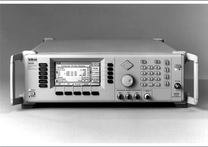
Figure 1-1. Typical Series 682XXB/683XXB Synthesized Signal Generator (Model 68369B Shown)

Chapter 1
General Information
1-1
1-2
SCOPE OF MANUAL |
This manual provides service information for all models of the Series |
|
682XXB/683XXB Synthesized Signal Generators. The service informa- |
|
tion includes replaceable parts information, functional circuit descrip- |
|
tions, block diagrams, performance verification tests, and procedures |
|
for calibration, troubleshooting, and assembly/subassembly removal |
|
and replacement. (Throughout this manual, the terms 682XXB/ |
|
683XXB and signal generator will be used interchangeably to refer to |
|
the instrument.) Manual organization is shown in the table of con- |
|
tents. |
|
NOTE |
|
Service information for the series 682XXB signal generators |
|
and series 683XXB signal generators is combined into one |
|
manual because identical model numbers of each series con- |
|
tain the same assemblies, subassemblies, and components. |
|
Differences between the series are noted where applicable |
|
throughout the manual. |
INTRODUCTION |
This chapter provides a general description of the Series 682XXB/ |
|
683XXB Synthesized Signal Generators, identification numbers, |
|
related manuals, and options. Information is included concerning level |
|
of maintenance, replaceable subassemblies and RF components, |
|
exchange assembly program, and preventive maintenance. Static- |
|
sensitive component handling precautions and lists of exchangeable |
|
subassemblies and recommended test equipment are also provided. |
1-3 DESCRIPTION |
The Series 682XXB Synthesized Signal Generator and the Series |
|
683XXB Synthesized Signal Generator are microprocessor-based, |
|
synthesized signal sources with high resolution phase-lock capability. |
|
They generate both discrete CW frequencies and broad (full range) |
|
and narrow band sweeps across the frequency range of 10 MHz to |
|
65 GHz. All functions of the signal generators are fully controllable |
|
locally from the front panel or remotely (except for power on/standby) |
|
via the IEEE-488 General Purpose Interface Bus (GPIB). |
|
The Series 682XXB Synthesized Signal Generator and the Series |
|
683XXB Synthesized Signal Generator each presently consists of 15 |
|
models covering a variety of frequency ranges and power levels. Table |
|
1-1, pages 1-4 and 1-5, lists models, frequency ranges, and maximum |
|
leveled output. |
682XXB/683XXB MM |
1-3 |

GENERAL |
682XXB/683XXB |
INFORMATION |
MODELS |
Table 1-1. Series 682XXB/683XXB Models (1 of 2)
68XXXB |
Frequency |
Output Power |
Output Power |
||
Model |
|
(GHz) |
w/Step Attenuator |
||
|
|
||||
|
|
|
|
||
68X37B |
2.0 – 20.0 GHz |
+13.0 dBm |
+11.0 dBm |
||
|
|
|
|
||
68X45B |
0.5 – 20.0 GHz |
+13.0 dBm |
+11.0 dBm |
||
|
|
|
|
|
|
68X47B |
0.01 |
– 20.0 GHz |
+13.0 dBm |
+11.0 dBm |
|
|
|
|
|
||
68X53B |
2.0 – 20.0 GHz |
+9.0 dBm |
+7.0 dBm |
||
20.0 |
– 26.5 GHz |
+6.0 dBm |
+3.5 dBm |
||
|
|||||
|
|
|
|
|
|
|
0.5 |
– 2.2 GHz |
+13.0 dBm |
+11.0 dBm |
|
68X55B |
2.2 – 20.0 GHz |
+9.0 dBm |
+7.0 dBm |
||
|
20.0 |
– 26.5 GHz |
+6.0 dBm |
+3.5 dBm |
|
|
|
|
|
||
|
0.01 – 2.0 GHz |
+13.0 dBm |
+11.0 dBm |
||
68X59B |
2.0 – 20.0 GHz |
+9.0 dBm |
+7.0 dBm |
||
|
20.0 |
– 26.5 GHz |
+6.0 dBm |
+3.5 dBm |
|
|
|
|
|
||
68X63B |
2.0 – 20.0 GHz |
+9.0 dBm |
+7.0 dBm |
||
20.0 |
– 40.0 GHz |
+6.0 dBm |
+3.0 dBm |
||
|
|||||
|
|
|
|
|
|
|
0.5 |
– 2.2 GHz |
+13.0 dBm |
+11.0 dBm |
|
68X65B |
2.2 – 20.0 GHz |
+9.0 dBm |
+7.0 dBm |
||
|
20.0 |
– 40.0 GHz |
+6.0 dBm |
+3.0 dBm |
|
|
|
|
|
||
|
0.01 – 2.0 GHz |
+13.0 dBm |
+11.0 dBm |
||
68X69B |
2.0 – 20.0 GHz |
+9.0 dBm |
+7.0 dBm |
||
|
20.0 |
– 40.0 GHz |
+6.0 dBm |
+3.0 dBm |
|
|
|
|
|
|
|
|
0.5 |
– 2.2 GHz |
+11.0 dBm |
+10.0 dBm |
|
68X75B |
2.2 – 20.0 GHz |
+10.0 dBm |
+8.5 dBm |
||
20.0 |
– 40.0 GHz |
+2.5 dBm |
0.0 dBm |
||
|
|||||
|
40.0 |
– 50.0 GHz |
+2.5 dBm |
–1.0 dBm |
|
|
|
|
|
||
|
0.01 – 2.0 GHz |
+12.0 dBm |
+10.0 dBm |
||
68X77B |
2.0 – 20.0 GHz |
+10.0 dBm |
+8.5 dBm |
||
20.0 |
– 40.0 GHz |
+2.5 dBm |
0.0 dBm |
||
|
|||||
|
40.0 |
– 50.0 GHz |
+2.5 dBm |
–1.0 dBm |
|
|
|
|
|
|
|
|
0.5 |
– 2.2 GHz |
+11.0 dBm |
+10.0 dBm |
|
|
2.2 – 20.0 GHz |
+10.0 dBm |
+8.5 dBm |
||
68X85B |
20.0 |
– 40.0 GHz |
+2.5 dBm |
0.0 dBm |
|
|
40.0 |
– 50.0 GHz |
+2.0 dBm |
–1.5 dBm |
|
|
50.0 |
– 60.0 GHz |
+2.0 dBm |
–2.0 dBm |
|
|
|
|
|
||
|
0.01 – 2.0 GHz |
+12.0 dBm |
+10.0 dBm |
||
|
2.0 – 20.0 GHz |
+10.0 dBm |
+8.5 dBm |
||
68X87B |
20.0 |
– 40.0 GHz |
+2.5 dBm |
0.0 dBm |
|
|
40.0 |
– 50.0 GHz |
+2.0 dBm |
–1.5 dBm |
|
|
50.0 |
– 60.0 GHz |
+2.0 dBm |
–2.0 dBm |
|
|
|
|
|
|
|
|
0.5 |
– 2.2 GHz |
+11.0 dBm |
|
|
|
2.2 – 20.0 GHz |
+10.0 dBm |
|
||
68X95B |
20.0 |
– 40.0 GHz |
+2.5 dBm |
Not Available |
|
|
40.0 |
– 50.0 GHz |
0.0 dBm |
|
|
|
50.0 |
– 65.0 GHz |
–2.0 dBm |
|
|
|
|
|
|
|
|
1-4 |
682XXB/683XXB MM |

GENERAL |
IDENTIFICATION |
INFORMATION |
NUMBER |
Table 1-1. Series 682XXB/683XXB Models (2 of 2)
|
68XXXB |
Frequency |
Output Power |
Output Power |
|
|
|
Model |
|
(GHz) |
w/Step Attenuator |
|
|
|
|
|
|
|||
|
|
|
|
|
|
|
|
|
0.01 – 2.0 GHz |
+12.0 dBm |
|
|
|
|
|
2.0 – 20.0 GHz |
+10.0 dBm |
|
|
|
|
68X97B |
20.0 |
– 40.0 GHz |
+2.5 dBm |
Not Available |
|
|
|
40.0 |
– 50.0 GHz |
0.0 dBm |
|
|
|
|
50.0 |
– 65.0 GHz |
–2.0 dBm |
|
|
|
|
|
|
|||
|
|
With Option 15B (High Power) Installed |
|
|||
|
|
|
|
|
|
|
|
68X37B |
2.0 – 20.0 GHz |
+17.0 dBm |
+15.0 dBm |
|
|
|
|
|
|
|
|
|
|
68X45B |
0.5 |
– 2.2 GHz |
+13.0 dBm |
+11.0 dBm |
|
|
2.2 – 20.0 GHz |
+17.0 dBm |
+15.0 dBm |
|
||
|
|
|
||||
|
|
|
|
|
|
|
|
68X47B |
0.01 – 2.0 GHz |
+13.0 dBm |
+11.0 dBm |
|
|
|
2.0 – 20.0 GHz |
+17.0 dBm |
+15.0 dBm |
|
||
|
|
|
||||
|
|
|
|
|
|
|
|
68X53B |
2.0 – 20.0 GHz |
+13.0 dBm |
+11.0 dBm |
|
|
|
20.0 |
– 26.5 GHz |
+10.0 dBm |
+7.5 dBm |
|
|
|
|
|
||||
|
|
|
|
|
|
|
|
|
0.5 |
– 2.2 GHz |
+13.0 dBm |
+11.0 dBm |
|
|
68X55B |
2.2 – 20.0 GHz |
+13.0 dBm |
+11.0 dBm |
|
|
|
|
20.0 |
– 26.5 GHz |
+10.0 dBm |
+7.5 dBm |
|
|
|
|
|
|
|
|
|
|
0.01 – 2.0 GHz |
+13.0 dBm |
+11.0 dBm |
|
|
|
68X59B |
2.0 – 20.0 GHz |
+13.0 dBm |
+11.0 dBm |
|
|
|
|
20.0 |
– 26.5 GHz |
+10.0 dBm |
+7.5 dBm |
|
|
|
|
|
|
|
|
|
68X63B |
2.0 – 20.0 GHz |
+13.0 dBm |
+11.0 dBm |
|
|
|
20.0 |
– 40.0 GHz |
+6.0 dBm |
+3.0 dBm |
|
|
|
|
|
||||
|
|
|
|
|
|
|
|
|
0.5 |
– 2.2 GHz |
+13.0 dBm |
+11.0 dBm |
|
|
68X65B |
2.2 – 20.0 GHz |
+13.0 dBm |
+11.0 dBm |
|
|
|
|
20.0 |
– 40.0 GHz |
+6.0 dBm |
+3.0 dBm |
|
|
|
|
|
|
|
|
|
|
0.01 – 2.0 GHz |
+13.0 dBm |
+11.0 dBm |
|
|
|
68X69B |
2.0 – 20.0 GHz |
+13.0 dBm |
+11.0 dBm |
|
|
|
|
20.0 |
– 40.0 GHz |
+6.0 dBm |
+3.0 dBm |
|
|
|
|
|
|
|
|
|
68X75B |
0.5 – 50.0 GHz |
Standard |
Standard |
|
|
|
|
|
|
|
|
|
|
68X77B |
0.01 |
– 50.0 GHz |
Standard |
Standard |
|
|
|
|
|
|
|
|
|
68X85B |
0.5 – 60.0 GHz |
Standard |
Standard |
|
|
|
|
|
|
|
|
|
|
68X87B |
0.01 |
– 60.0 GHz |
Standard |
Standard |
|
|
|
|
|
|
|
|
|
68X95B |
0.5 - 65.0 GHz |
Standard |
Not Available |
|
|
|
|
|
|
|
|
|
|
68X97B |
0.01 |
– 65.0 GHz |
Standard |
Not Available |
|
|
|
|
|
|
|
|
1-4 IDENTIFICATION |
All ANRITSU instruments are assigned a unique six-digit ID number, |
NUMBER |
such as “403002.” The ID number is imprinted on a decal that is af- |
|
fixed to the rear panel of the unit. Special-order instrument configura- |
|
tions also have an additional special serial number tag attached to the |
|
rear panel of the unit. |
682XXB/683XXB MM |
1-5 |

GENERAL |
ELECTRONIC |
INFORMATION |
MANUAL |
|
|
When ordering parts or corresponding with ANRITSU Customer Serv- |
|
|
|
ice, please use the correct serial number with reference to the specific |
|
|
|
instrument’s model number (i.e., Model 68347B Synthesized Signal |
|
|
|
Generator, Serial No. 403002). |
|
1-5 |
ELECTRONIC MANUAL |
This manual is available on CD ROM as an Adobe Acrobat Portable |
|
|
|
Document Format ( .pdf) file. The file can be viewed using Acrobat |
|
|
|
Reader, a free program that is also included on the CD ROM. The file |
|
|
|
is “linked” such that the viewer can choose a topic to view from the |
|
|
|
displayed “bookmark” list and “jump” to the manual page on which the |
|
|
|
topic resides. The text can also be word-searched. Contact ANRITSU |
|
|
|
Customer Service for price and availability. |
|
1-6 |
RELATED MANUALS |
This is one of a four manual set that consists of an Operation Manual, |
|
|
|
a GPIB Programming Manual, a SCPI Programming Manual, and a |
|
|
|
Maintenance Manual. |
|
|
|
Operation |
This manual provides information and instructions |
|
|
Manual |
for operation of the series 682XXB/683XXB signal |
|
|
|
generators using the front panel controls. It also in- |
|
|
|
cludes general information, performance specifica- |
|
|
|
tions, installation instructions, and operation |
|
|
|
verification procedures. The ANRITSU part number |
|
|
|
for the Operation Manual is 10370-10284. |
|
|
GPIB |
This manual provides information for remote opera- |
|
|
Programming |
tion of the series 682XXB/683XXB signal generators |
|
|
Manual |
using Product Specific commands sent from an ex- |
|
|
|
ternal controller via the IEEE 488 General Purpose |
|
|
|
Interface Bus (GPIB). It contains a complete listing |
|
|
|
and description of all 682XXB/683XXB GPIB Prod- |
|
|
|
uct Specific commands and several programming |
|
|
|
examples. The ANRITSU part number for the GPIB |
|
|
|
Programming Manual is 10370-10286. |
|
|
SCPI |
This manual provides information for remote opera- |
|
|
Programming |
tion of the series 682XXB/683XXB signal generators |
|
|
Manual |
using Standard Commands for Programmable In- |
|
|
|
struments (SCPI) commands sent from an external |
|
|
|
controller via the IEEE 488 General Purpose Inter- |
|
|
|
face Bus (GPIB). It contains a complete listing and |
description of each command in the 682XXB/ 683XXB SCPI command set and examples of command usage. The ANRITSU part number for the SCPI Programming Manual is 10370-10288.
1-6 |
682XXB/683XXB MM |

GENERAL |
OPTIONS |
INFORMATION |
|
1-7 OPTIONS |
The following instrument options are available. |
qOption 1, Rack Mounting. Rack mount kit containing a set of track slides (90 tilt capability), mounting ears, and front panel handles for mounting the instrument in a standard 19-inch equipment rack.
qOption 2A, 110 dB Step Attenuator. Adds a 10 dB per step attenuator with a 110 dB range for models having a high-end frequency of 26.5 GHz. Output power is selected directly in dBm on the front panel (or via GPIB). Rated output power is reduced.
qOption 2B, 110 dB Step Attenuator. Adds a 10 dB per step attenuator with a 110 dB range for models having a high-end frequency of 40 GHz. Output power is selected directly in dBm on the front panel (or via GPIB). Rated output power is reduced.
qOption 2C, 90 dB Step Attenuator. Adds a 10 dB per step attenuator with a 90 dB range for models having a high-end frequency of 50 GHz. Output power is selected directly in dBm on the front panel (or via GPIB). Rated output power is reduced.
qOption 2D, 90 dB Step Attenuator. Adds a 10 dB per step attenuator with a 90 dB range for models having a high-end frequency of 60 GHz. Output power is selected directly in dBm on the front panel (or via GPIB). Rated output power is reduced.
qOption 6, Phase Modulation ( M). Adds phase modulation capability. The internal FM generator becomes the FM/ M generator. (Not available in combination with Option 7.)
qOption 7, Delete AM/FM Generator. Deletes the internal AM and FM generators. External AM and FM capability remains unchanged. (Not available in combination with Option 8 or Option 20.)
qOption 8, Internal Power Meter. Adds an internal power meter that is compatible with ANRITSU 560-7, 5400-71, or 640071 series detectors. (Not available in combination with Option 7.)
qOption 9, Rear Panel RF Output. Moves the RF output connector to the rear panel.
qOption 11, 0.1 Hz Frequency Resolution. Provides frequency resolution of 0.1 Hz.
qOption 14, ANRITSU 360B VNA Compatibility. Modifies rack mounting hardware to mate unit in a ANRITSU 360B VNA console.
qOption 15B, High Power Output. Adds high-power RF components to the instrument providing increased RF output power in the 2–26.5 GHz frequency range. Option 15B is standard in models having a high-end frequency that is >40 GHz.
qOption 16, High-Stability Time Base. Adds an ovenized,
10 MHz crystal oscillator with <5 x 10⁻¹⁰/day frequency stability.
682XXB/683XXB MM |
1-7 |

GENERAL |
LEVEL OF |
INFORMATION |
MAINTENANCE |
q Option 17A, No Front Panel. Deletes the front panel for use in remote control applications where a front panel display or keyboard control are not needed.
|
q Option 18, mmWave Module Bias Output. Provides bias out- |
|
|
put for 54000-xWRxx Millimeter Wave Source Modules. BNC |
|
|
Twinax connector, rear panel. |
|
|
q Option 19, SCPI Programmability. Adds GPIB command |
|
|
mnemonics complying with Standard Commands for Program- |
|
|
mable Instruments (SCPI), Version 1993. SCPI programming |
|
|
complies with IEEE 488.2-1987. |
|
|
q Option 20, SCAN Modulator. Adds an internal SCAN modula- |
|
|
tor for simulating high-depth amplitude modulated signals in |
|
|
models 68237B/68337B, 68245B/68345B, and 68247B/68347B |
|
|
only. Requires an external modulating signal. (Not available in |
|
|
combination with Option 7.) |
|
1-8 LEVEL OF |
Maintenance of the 682XXB/683XXB consists of: |
|
MAINTENANCE |
q Troubleshooting the instrument to a replaceable subassembly or |
|
|
||
|
RF component. |
|
|
q Repair by replacing the failed subassembly or RF component. |
|
|
q Calibration. |
|
|
q Preventive maintenance. |
|
|
Troubleshoot- |
The 682XXB/683XXB firmware includes internal |
|
ing |
diagnostics that self-test most of the internal assem- |
|
|
blies of the instrument. When the signal generator |
|
|
fails self-test, one or more error messages are dis- |
|
|
played to aid in troubleshooting the failure to a |
|
|
replaceable subassembly or RF component. Chapter |
|
|
5 lists and describes the self-test error messages |
|
|
and provides procedures for isolating 682XXB/ |
|
|
683XXB failures to a replaceable subassembly or RF |
|
|
component. |
|
Repair |
Most instrument failures are field repairable by re- |
|
|
placing the failed subassembly or RF component. |
|
|
Detailed instructions for removing and replacing |
|
|
failed subassemblies and components are provided |
|
|
in Chapter 6. |
|
Calibration |
The signal generator may require calibration after |
|
|
repair. Refer to Chapter 4 for a listing of calibration |
|
|
requirements and calibration procedures. |
|
Preventive |
Preventive maintenance on the 682XXB/683XXB |
|
Maintenance |
consists of cleaning the fan honeycomb filter, de- |
|
|
scribed in paragraph 1-8. |
1-8 |
682XXB/683XXB MM |
GENERAL |
PREVENTIVE |
INFORMATION |
MAINTENANCE |
1-9 PREVENTIVE |
The 682XXB/683XXB must always receive adequate ventilation. A |
|
MAINTENANCE |
blocked fan filter can cause the instrument to overheat and shut down. |
|
|
Check and clean the rear panel fan honeycomb filter periodically. |
|
|
Clean the fan honeycomb filter more frequently in dusty environ- |
|
|
ments. Clean the filter as follows. |
|
|
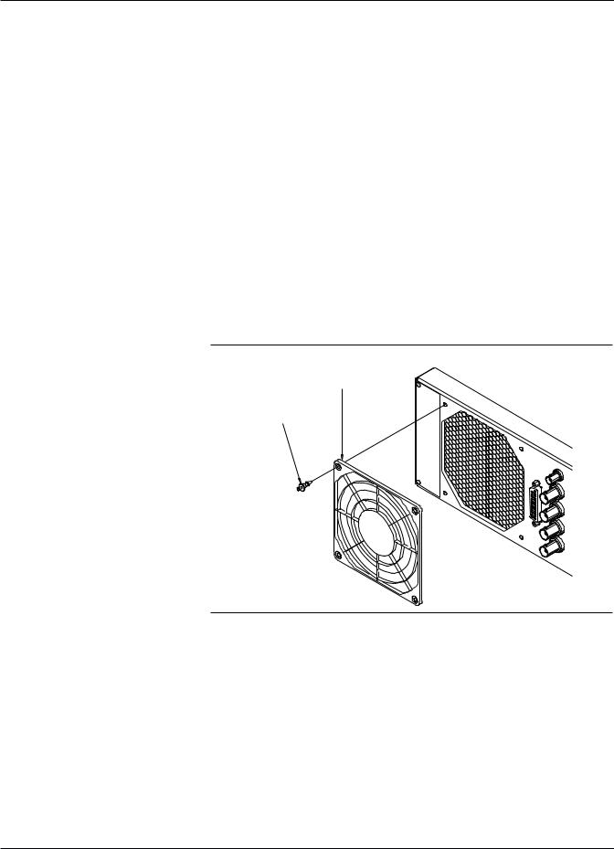
Step 1 |
Remove the filter guard from the rear panel by pull- |
|
|
ing out on the four panel fasteners holding them in |
|
|
place (Figure 1-2). |
|
Step 2 |
Vacuum the honeycomb filter to clean it. |
|
Step 3 |
Install the filter guard back on the rear panel. |
|
Step 4 |
Press in on the panel fasteners to secure the filter |
|
|
guard to the rear panel. |
|
Figure 1-2. Removing/Replacing the Fan Filter Guard |
1-10 STATIC-SENSITIVE |
The 682XXB/683XXB contains components that can be damaged by |
COMPONENT |
static electricity. Figure 1-3 illustrates the precautions that should be |
HANDLING |
followed when handling static-sensitive subassemblies and compo- |
PRECAUTIONS |
nents. If followed, these precautions will minimize the possibilities of |
|
static-shock damage to these items. |
|
NOTE |
|
Use of a grounded wrist strap when removing and/or replac- |
|
ing subassemblies or components is strongly recommended. |
682XXB/683XXB MM |
1-9 |

GENERAL |
STATIC-SENSITIVE COMPONENT |
|
INFORMATION |
HANDLING PRECAUTIONS |
|
|
|
|
1. Do not touch exposed contacts on any static sensitive component.
4. Wear a static-discharge wristband when working with static sensitive components.
7. Handle PCBs only by their edges. Do not handle by the edge connectors.
2. Do not slide static sensitive component across any surface.
5. Label all static sensitive devices.
8. Lift & handle solid state devices by their bodies – never by their leads.
3. Do not handle static sensitive components in areas where the floor or work surface covering is capable of generating a static charge.
6. Keep component leads shorted together whenever possible.
9. Transport and store PCBs and other static sensitive devices in static-shielded containers.
10.ADDITIONAL PRECAUTIONS:
Keep workspaces clean and free of any objects capable of holding or storing a static charge.
Connect soldering tools to an earth ground.
Use only special anti-static suction or wick-type desoldering tools.
Figure 1-3. Static-Sensitive Component Handling Precautions
1-10 |
682XXB/683XXB MM |
GENERAL |
START UP |
INFORMATION |
CONFIGURATION |
1-11 STARTUP |
The 682XXB/683XXB comes from the factory with a jumper across |
||||||
CONFIGURATIONS |
pins 2 and 3 of front panel connector J12 (Figure 1-4). In this configu- |
||||||
|
ration, connecting the instrument to line power automatically places it |
||||||
|
in operate mode (front panel OPERATE LED on). |
||||||
|
The startup configuration can be changed so that the signal generator |
||||||
|
comes up in standby mode (front panel STANDBY LED on) when it is |
||||||
|
connected to line power. Change the startup configuration as follows: |
||||||
|
Step 1 |
Disconnect the instrument from line power. |
|||||
|
Step 2 |
Remove the top cover from the 682XXB/683XXB. |
|||||
|
|
(Refer to Chapter 6 for instructions). |
|||||
|
Step 3 |
Locate front panel connector J12 and remove the |
|||||
|
|
jumper from across pins 2 and 3. It is located on the |
|||||
|
|
A2A1 PCB which plugs into the Front Panel Assem- |
|||||
|
|
bly. |
|||||
|
Step 4 |
Install the jumper across pins 1 and 2 of connector |
|||||
|
|
J12. |
|||||
|
Step 5 |
Install the top cover and connect the signal genera- |
|||||
|
|
tor to line power. The instrument should come up in |
|||||
|
|
standby mode. |
|||||
|
|
|
|
|
|
|
|
|
|
|
|
|
|
|
|
|
|
|
|
|
|
|
|
|
|
|
|
|
|
|
|
|
|
|
|
|
|
|
|
|
|
|
|
|
|
|
|
|
|
|
|
|
|
|
|
Figure 1-4. Startup Configuration of Connector J12
682XXB/683XXB MM |
1-11 |

GENERAL |
RECOMMENDED |
INFORMATION |
TEST EQUIPMENT |
1-12 RECOMMENDED TEST |
Table 1-2 provides a list of recommended test equipment needed for |
EQUIPMENT |
the performance verification, calibration, and troubleshooting proce- |
|
dures presented in this manual. |
Table 1-2. Recommended Test Equipment (1 of 3)
INSTRUMENT |
CRITICAL |
RECOMMENDED |
USAGE (1) |
||
SPECIFICATION |
MANUFACTURER/MODEL |
||||
|
|||||
Spectrum Analyzer, |
Frequency Range: 0.01 to 65 GHz |
Tektronix, Model 2794, with |
C, P, T |
||
with |
Resolution Bandwidth: 10 Hz |
External Mixers: |
|
|
|
External Mixers |
|
WM780K (18 to 26.5 GHz) |
|
|
|
and |
|
WM780A (26.5 to 40 GHz) |
|
|
|
Diplexer Assy |
|
WM780U (40 to 60 GHz) |
|
|
|
|
|
WM780E (60 to 90 GHz) |
|
|
|
|
|
Diplexer Assy: 015-0385-00 |
|
|
|
|
|
|
|
|
|
Spectrum Analyzer |
Frequency Range: 20 Hz to 40 MHz |
Hewlett-Packard, Model 3585B |
P |
||
|
Resolution Bandwidth: 3 Hz |
|
|
|
|
|
|
|
|
|
|
Frequency Counter |
Frequency Range: 0.01 to 65 GHz |
EIP Microwave, Inc. Models 538B, 548B, |
C, P |
||
with |
Input Impedance: 50W |
or 578B, with |
|
|
|
Cable Kit |
Resolution: 1 Hz |
Cable Kit: Option 590 |
|
|
|
and |
Other: External Time Base Input |
and |
|
|
|
External Mixer |
|
External Mixer: |
|
|
|
|
|
Option 91 (26.5 to 40 GHz) |
|
|
|
|
|
Option 92 (40 to 60 GHz) |
|
|
|
|
|
Option 93 (60 to 90 GHz) |
|
|
|
|
|
|
|
|
|
Power Meter, |
Power Range: –30 to +20 dBm |
Hewlett-Packard Model 437B, with |
C, P |
||
with Power Sensor |
(1mW to 100mW) |
Power Sensor: |
|
|
|
|
|
HP 8487A (0.01 to 50 GHz) |
|
|
|
|
|
|
|
|
|
Power Meter, |
Power Range: –30 to +20 dBm |
ANRITSU ML4803A, with |
C, P |
||
with Power Sensor |
(1mW to 100mW) |
Power Sensor: |
|
|
|
|
|
MP716A4 (50 to 75 GHz) |
|
|
|
|
|
|
|
|
|
Digital Multimeter |
Resolution: 4-1/2 digits (to 20V) |
John Fluke, Inc., Model 8840A, with |
C, T |
||
|
DC Accuracy: 0.002% +2 counts |
Option 8840A-09K (True RMS AC) |
|
|
|
|
DC Input Impedance: 10 MW |
|
|
|
|
|
AC Accuracy: 0.07% +100 counts |
|
|
|
|
|
(to 20 kHz) |
|
|
|
|
|
AC Input Impedance: 1 MW |
|
|
|
|
|
|
|
|
|
|
Frequency Reference |
Frequency: 10 MHz |
Absolute Time Corp., Model 300 |
P |
||
|
Accuracy: 5 x 10-12 parts/day |
|
|
|
|
Frequency Standard |
Frequency: 10 MHz |
Spectracom Corp., Model 8161 |
C |
||
|
Accuracy: 1 ´ 10–10 parts/day |
|
|
|
|
Function Generator |
Output Voltage: 2 volts peak-to-peak |
Hewlett-Packard, Model 8116A |
C |
||
|
Functions: 0.1 Hz to 100 kHz sine and |
|
|
|
|
|
square waveforms |
|
|
|
|
|
|
|
|
|
|
Function Generator |
Output Voltage: 2 volts peak-to-peak |
Hewlett-Packard, Model 33120A |
C |
||
|
Functions: 0.1 Hz to 100 kHz sine and |
|
|
|
|
|
square waveforms |
|
|
|
|
|
|
|
|
|
|
1-12 |
682XXB/683XXB MM |

GENERAL |
RECOMMENDED |
INFORMATION |
TEST EQUIPMENT |
Table 1-2. Recommended Test Equipment (2 of 3)
INSTRUMENT |
CRITICAL |
RECOMMENDED |
USAGE (1) |
||
SPECIFICATION |
MANUFACTURER/MODEL |
||||
|
|||||
Modulation Analyzer |
Frequency Input: 10 MHz |
Hewlett-Packard, Model 8901A |
P |
||
|
(or the IF of the Spectrum Analyzer) |
|
|
|
|
|
AM Depth: 0% to 90% |
|
|
|
|
|
AM Modulation Rates: DC to 100 kHz |
|
|
|
|
|
Filters: 20 kHz lowpass, 300 Hz highpass |
|
|
|
|
|
|
|
|
|
|
Oscilloscope |
Bandwidth: DC to 150 MHz |
Tektronix, Inc. Model TAS485 |
P, T |
||
|
Vertical Sensitivity: 2mV/division |
|
|
|
|
|
Horizontal Sensitivity: 50 ns/division |
|
|
|
|
|
|
|
|
|
|
Mixer |
Frequency Range: 1 to 26 GHz |
Macom Micro Electronics Div. |
P |
||
|
|
Model DMS1-26A |
|
|
|
|
|
|
|
|
|
Scalar Network |
Frequency Range: 0.01 to 50 GHz |
ANRITSU, Model 562, with |
C, T |
||
Analyzer, with |
|
RF Detector: |
|
|
|
RF Detector |
|
560-7K50 (0.01 to 40 GHz) |
|
|
|
|
|
560-7VA50 (0.01 to 50 GHz) |
|
|
|
|
|
SC5198 (40 to 60 GHz) |
|
|
|
|
|
|
|
|
|
Adapter |
K (male) to 2.4 mm (female) |
Hewlett-Packard |
C, P |
||
|
Adapts the Power Sensor, HP 8487A, to |
Part Number: HP 11904D |
|
|
|
|
the 682XXB/683XXB RF OUTPUT con- |
|
|
|
|
|
nector (£40 GHz models) |
|
|
|
|
|
|
|
|
|
|
Adapter |
Adapts the MP716A4 Power Sensor to |
ANRITSU MA4002B |
C, P |
||
|
the ML4803A Power Meter |
|
|
|
|
|
|
|
|
|
|
Adapter |
WR15 to V (male) |
ANRITSU, Model 35WR15V |
C, P |
||
|
Adapts the MP716A4 Power Sensor to |
|
|
|
|
|
the 682XXB/683XXB RF OUTPUT |
|
|
|
|
|
connector (>40 GHz models) |
|
|
|
|
|
|
|
|
|
|
Attenuator |
Frequency Range: DC to 40 GHz |
ANRITSU, Model 41KC-10 |
C, P |
||
|
Max Input Power: >+17 dBm |
|
|
|
|
|
Attenuation: 10 dB |
|
|
|
|
|
|
|
|
|
|
Attenuator |
Frequency Range: DC to 40 GHz |
ANRITSU, Model 41KC-20 |
P |
||
|
Max Input Power: >+17 dBm |
|
|
|
|
|
Attenuation: 20 dB |
|
|
|
|
|
|
|
|
|
|
Attenuator |
Frequency Range: DC to 60 GHz |
ANRITSU, Model 41V-10 |
C, P |
||
|
Max Input Power: >+17 dBm |
|
|
|
|
|
Attenuation: 10 dB |
|
|
|
|
|
|
|
|
|
|
Attenuator |
Frequency Range: DC to 60 GHz |
ANRITSU, Model 41V-20 |
P |
||
|
Max Input Power: >+17 dBm |
|
|
|
|
|
Attenuation: 20 dB |
|
|
|
|
|
|
|
|
|
|
RF Detector |
Frequency Range: 0.01 to 40 GHz |
ANRITSU, Model 75KC50 |
T |
||
|
Output Polarity: Negative |
(K input/BNC output connectors) |
|
|
|
|
|
|
|
|
|
RF Detector |
Frequency Range: 0.01 to 50 GHz |
ANRITSU, Model 75VA50 |
T |
||
|
Output Polarity: Negative |
(V input/BNC output connectors) |
|
|
|
|
|
|
|
|
|
682XXB/683XXB MM |
1-13 |

GENERAL |
EXCHANGE |
INFORMATION |
ASSEMBLY PROGRAM |
Table 1-2. Recommended Test Equipment (3 of 3)
INSTRUMENT |
CRITICAL |
RECOMMENDED |
USAGE (1) |
|
SPECIFICATION |
MANUFACTURER/MODEL |
|||
|
||||
Microwave (Pulse) |
Output Polarity: Negative |
ANRITSU, Model SC3800 |
P |
|
Detector |
Frequency Range: 0.01 to 40 GHz |
(K input/BNC output connectors) |
|
|
|
|
|
|
|
High Pass Filter |
150 MHz High-Pass Filter (DC Block) |
Narda, Model 4564 |
P |
|
|
|
|
|
|
Low Pass Filter |
450 MHz Low-Pass Filter |
Mini-Circuits, Model SLP-450 |
P |
|
|
|
|
|
|
Personal Computer |
PC Configuration: IBM AT or compatible |
Any common source |
C |
|
|
Operating System: Windows 3.1 |
|
|
|
|
Accessories: Mouse |
|
|
|
|
|
|
|
|
Serial Interface Assy |
Provides serial interface between the PC |
ANRITSU P/N: T1678 |
C |
|
|
and the 682XXB/683XXB. |
|
|
|
|
|
|
|
|
Tee |
Connectors: 50W BNC |
Any common source |
C, P |
|
|
|
|
|
|
Cables |
Connectors: 50W BNC |
Any common source |
C, P, T |
|
|
|
|
|
NOTES: (1) P = Performance Verification Tests (Chapter 3); C = Calibration (Chapter 4); T = Troubleshooting (Chapter 5)
1-13
1-14
EXCHANGE |
ANRITSU maintains an exchange assembly program for selected |
ASSEMBLY PROGRAM |
682XXB/683XXB subassemblies and RF components. If a malfunction |
|
occurs in one of these subassemblies, the defective unit can be ex- |
|
changed. Upon receiving your request, ANRITSU will ship the ex- |
|
change subassembly or RF component to you, typically within 24 |
|
hours. You then have 45 days in which to return the defective item. All |
|
exchange subassemblies or RF components are warranted for 90 days |
|
from the date of shipment, or for the balance of the original equipment |
|
warranty, whichever is longer. |
|
Please have the exact model number and serial number of your unit |
|
available when requesting this service, as the information about your |
|
unit is filed according to the instrument’s model and serial number. |
|
For more information about the program, contact your local sales rep- |
|
resentative or call your local ANRITSU service center. Refer to Table |
|
1-5, on page 1-18, for a list of current ANRITSU service centers. |
REPLACEABLE |
Table 1-3 lists those replaceable subassemblies and RF components of |
SUBASSEMBLIES |
the 682XXB/683XXB that are presently covered by the ANRITSU ex- |
AND PARTS |
change assembly program. Table 1-4, on page 1-16, lists common re- |
|
placeable parts for the 682XXB/683XXB that are not presently on the |
|
exchange assembly program. |
|
All parts listed in Tables 1-3 and 1-4 may be ordered from your local |
|
ANRITSU service center. |
1-14 |
682XXB/683XXB MM |

GENERAL |
|
INFORMATION |
PARTS LIST |
Table 1-3. Replaceable Subassemblies and RF Components (1 of 2)
|
|
SUBASSEMBLY OR PART NAME |
ANRITSU PART NUMBER |
|
|
|
|
|
|
|
|
|
|
|
|
|
Printed Circuit Board Assemblies |
|
|
|
|
|
|
|
|
Front Panel Assy 683XXB |
ND40832 |
|
|
|
Front Panel Assy 682XXB |
ND40833 |
|
|
|
A3 Reference Loop PCB Assy |
D37436-3 |
|
|
|
A4 Coarse Loop PCB Assy |
D40604-3 |
|
|
|
A4 Coarse Loop PCB Assy |
D40634-3 |
|
|
|
A5 Fine Loop PCB Assy |
D37452-3 |
|
|
|
A5 Fine Loop PCB Assy |
D40605-3 |
|
|
|
A5 |
Fine Loop PCB Assy (w/Option 11) |
ND39917 |
|
|
A5 Fine Loop PCB Assy |
D40635-3 |
|
|
|
A5 |
Fine Loop PCB Assy (w/Option 11) |
D40635-7 |
|
|
A6 |
Pulse Generator PCB Assy |
D40606-3 |
|
|
A6 |
Pulse Generator PCB Assy |
D40626-3 |
|
|
A7 YIG Loop PCB Assy |
D40607-3 |
|
|
|
A7 YIG Loop PCB Assy |
D40637-3 |
|
|
|
A8 |
Function Generator PCB Assy |
D37408-3 |
|
|
A8 |
Function Generator PCB Assy |
D40608-3 |
|
|
A9 |
PIN Control PCB Assy |
D40609-3 |
|
|
A9 |
PIN Control PCB Assy |
D40629-3 |
|
|
A9 |
PIN Control PCB Assy |
D40639-3 |
|
|
A10 ALC PCB Assy |
D40610-3 |
|
|
|
A11 FM PCB Assy |
D40611-3 |
|
|
|
A11 FM PCB Assy |
D40641-3 |
|
|
|
A11 FM PCB Assy (w/Option 6) |
D40641-4 |
|
|
|
A12 Analog Instruction PCB Assy |
D37448-3 |
|
|
|
A12 Analog Instruction PCB Assy (682XXB) |
D40612-3 |
|
|
|
A13 YIG Driver PCB Assy |
D40613-3 |
|
|
|
A14 SDM Driver PCB Assy, 26.5 GHz |
D40614-4 |
|
|
|
A14 SDM, SQM Driver PCB Assy |
D40614-3 |
|
|
|
A15 Regulator PCB Assy |
D40615-3 |
|
|
|
A16 CPU Interface PCB Assy |
D37416-3 |
|
|
|
A17 CPU PCB Assy |
D37444-3 |
|
|
|
A18 Power Supply PCB Assy |
D40618-3 |
|
|
|
A19 Line Conditioner PCB Assy |
D40619-3 |
|
|
|
A21 Line Filter/Rectifier PCB Assy |
ND39918 |
|
|
|
A21-1 BNC/AUX I/O Connector PCB Assy |
ND39919 |
|
|
|
10 MHz Crystal Oscillator Assy |
D37332 |
|
|
682XXB/683XXB MM |
1-15 |

GENERAL |
|
INFORMATION |
PARTS LIST |
Table 1-3. Replaceable Subassemblies and RF Components (2 of 2)
|
SUBASSEMBLY OR PART NAME |
ANRITSU PART NUMBER |
|
|
|
|
|
|
|
|
|
|
RF Components |
|
|
|
|
|
|
|
YIG-Tuned Oscillator, 2 to 20 GHz |
C27327 |
|
|
Down Converter |
D27330 |
|
|
Pulsed Digital Down Converter |
D27370 |
|
|
Switched Doubler Module, 20 to 26.5 GHz |
ND40843 |
|
|
Switched Doubler Module, 20 to 40 GHz |
D28535 |
|
|
Source Quadrupler Module, 40 to 50 GHz |
D28185 |
|
|
Source Quadrupler Module, 40 to 60 GHz |
60-141 |
|
|
Source Quadrupler Module, 40 to 65 GHz |
60-142 |
|
|
Forward Coupler, 60 GHz and 65 GHz |
C27184 |
|
|
Coupler, 40 GHz |
D27115 |
|
|
Coupler, 60 GHz |
D27350 |
|
|
Pulsed Switched Filter |
D25015 |
|
|
Pulsed Switched Filter |
D29391 |
|
|
Pulsed Switched Filter (w/Option 15B) |
D26350 |
|
|
Pulsed Switched Filter (w/Option 15B) |
D29392 |
|
|
Output Connector Assy, K female |
ND39077 |
|
|
Output Connector Assy, V female |
ND40835 |
|
|
Step Attenuator, 110 dB, 26.5 GHz |
D27152 |
|
|
Step Attenuator, 110 dB, 40 GHz |
D25080 |
|
|
Step Attenuator, 90 dB, 50 GHz |
D27315 |
|
|
Step Attenuator, 90 dB, 60 GHz |
D28957 |
|
|
|
|
|
Table 1-4. Common Replaceable Subassemblies and Parts (1 of 2)
SUBASSEMBLY OR PART NAME |
ANRITSU PART NUMBER |
|
|
Cap, Protective (for RF Output Connector) |
A20304 |
Cover, Top |
D37131 |
Cover, Bottom |
D37135 |
Cover, Side |
D37133 |
Cover, Side Handle |
761-67 |
Cover, CPU Housing |
C37063 |
Cover, Main Card Cage |
D37064 |
Cover, Power Supply Housing |
C37062 |
EMI Gasket for side covers |
790-437 |
EMI Gasket for side covers |
790-390 |
EMI Gasket for Front Panel Assy |
790-223 |
1-16 |
682XXB/683XXB MM |

GENERAL |
|
INFORMATION |
PARTS LIST |
Table 1-4. Common Replaceable Subassemblies and Parts (2 of 2)
|
SUBASSEMBLY OR PART NAME |
ANRITSU PART NUMBER |
|
|
|
|
|
|
Fan Assembly |
A40513 |
|
|
Fan Mount |
790-425 |
|
|
Fan Membrane (Honey Comb Filter) |
C37137 |
|
|
Fan Grill |
790-426 |
|
|
Fasteners (for Fan Grill) |
790-433 |
|
|
Fuse, 5A, 3AG Slow Blow (110 Vac) |
631-33 |
|
|
Fuse, 2.5A, 3AG Slow Blow (230 Vac) |
631-14 |
|
|
Gasket, RFI (“O”rings for MCX connectors) |
790-393 |
|
|
Handle, Side Carrying |
783-830 |
|
|
Screw, Handle Side Carrying |
900-714 |
|
|
Line Module |
260-11 |
|
|
Shield Cover |
D37228 |
|
|
Shield |
D37229 |
|
|
Standoff |
785-922 |
|
|
Tape |
850-70 |
|
|
Foot, Rear Bottom Left |
2000-548 |
|
|
Foot, Rear Bottom Right |
2000-549 |
|
|
Foot, Rear Top Left |
2000-552 |
|
|
Foot, Rear Top Right |
2000-553 |
|
|
Screw, Green Head |
2000-560 |
|
|
|
|
|
|
682XXB/683XXB without Front Handles Installed |
|
|
|
|
|
|
|
Foot, Front Bottom Left |
2000-546 |
|
|
Foot, Front Bottom Right |
2000-547 |
|
|
Foot, Front Top Left |
2000-550 |
|
|
Foot, Front Top Right |
2000-551 |
|
|
|
|
|
|
682XXB/683XXB with Front Handles Installed |
|
|
|
|
|
|
|
Upper Insert |
B37147 |
|
|
Foot, Bottom Left |
C37170 |
|
|
Foot,Bottom Right |
C37171 |
|
|
Handle, Left |
D37168-2 |
|
|
Handle, Right |
D37169-2 |
|
|
Tilt Bail |
790-435 |
|
682XXB/683XXB MM |
1-17 |

GENERAL |
ANRITSU |
INFORMATION |
SERVICE CENTERS |
Table 1-5. ANRITSU Service Centers
UNITED STATES |
FRANCE |
JAPAN |
ANRITSU COMPANY |
ANRITSU S.A |
ANRITSU CUSTOMER SERVICE LTD. |
490 Jarvis Drive |
9 Avenue du Quebec |
1800 Onna Atsugi-shi |
Morgan Hill, CA 95037-2809 |
Zone de Courtaboeuf |
Kanagawa-Prf. 243 Japan |
Telephone: (408) 776-8300 |
91951 Les Ulis Cedex |
Telephone: 0462-96-6688 |
1-800-ANRITSU |
Telephone: 016-09-21-550 |
FAX: 0462-25-8379 |
FAX: 408-776-1744 |
FAX: 016-44-61-065 |
|
|
GERMANY |
SINGAPORE |
ANRITSU COMPANY |
ANRITSU GmbH |
ANRITSU (SINGAPORE) PTE LTD. |
10 New Maple Ave., Unit 305 |
Grafenberger Allee 54-56 |
10, Hoe Chiang Road |
Pine Brook, NJ 07058 |
D-40237 Dusseldorf, Germany |
#07-01/02 Keppel Towers |
Telephone: (973) 227-8999 |
Telephone: 0211-968550 |
Singapore 089315 |
1-800-ANRITSU |
FAX: 0211-9685555 |
Telephone: 282-2400 |
FAX: 973-575-0092 |
|
FAX: 282-2533 |
|
INDIA |
SOUTH AFRICA |
ANRITSU COMPANY |
MEERA AGENCIES PVT. LTD. |
ETECSA |
1155 E. Collins Blvd |
23 Community Centre |
12 Surrey Square Office Park |
Richardson, TX 75081 |
Zamroodpur, Kailash Colony Extension, |
330 Surrey Avenue |
Telephone: 1-800-ANRITSU |
New Delhi, India 110 048 |
Ferndale, Randburt, 2194 |
FAX: 972-671-1877 |
Phone: 011-2-6442700/6442800 |
South Africa |
|
FAX : 011-2-644250023 |
Telephone: 011-27-11-787-7200 |
|
|
FAX: 011-27-11-787-0446 |
AUSTRALIA |
ISRAEL |
SWEDEN |
ANRITSU PTY. LTD. |
TECH-CENT, LTD. |
ANRITSU AB |
Unit 3, 170 Foster Road |
4 Raul Valenberg St |
Botivid Center |
Mt Waverley, VIC 3149 |
Tel-Aviv 69719 |
Fittja Backe 13A |
Australia |
Telephone: (03) 64-78-563 |
145 84 Stockholmn |
Telephone: 03-9558-8177 |
FAX: (03) 64-78-334 |
Telephone: (08) 534-707-00 |
FAX: 03-9558-8255 |
|
FAX: (08) 534-707-30 |
BRAZIL
ANRITSU ELECTRONICA LTDA. Praia de Botafogo, 440, Sala 2401
CEP22250-040, Rio de Janeiro, RJ, Brasil Telephone: 021-527-6922
FAX: 021-53-71-456
CANADA
ANRITSU INSTRUMENTS LTD.
700 Silver Seven Road, Suite 120
Kanata, Ontario K2V 1C3
Telephone: (613) 591-2003
FAX: (613) 591-1006
CHINA
ANRITSU ELECTRONICS (SHANGHAI) CO. LTD.
2F, Rm B, 52 Section Factory Building
No. 516 Fu Te Rd (N)
Shanghai 200131 P.R. China
Telephone:21-58680226, 58680227, 58680228
FAX: 21-58680588
ITALY |
TAIWAN |
ANRITSU Sp.A |
ANRITSU CO., INC. |
Roma Office |
7F, No. 316, Section 1 |
Via E. Vittorini, 129 |
NeiHu Road |
00144 Roma EUR |
Taipei, Taiwan, R.O.C. |
Telephone: (06) 50-99-711 |
Telephone: 886-2-8751-1816 |
FAX: (06) 50-22-4252 |
FAX: 886-2-8751-2126 |
KOREA |
UNITED KINGDOM |
ANRITSU CORPORATION LTD. |
ANRITSU LTD. |
Head Office: |
200 Capability Green |
14F, Hyunjuk Building 832-41 |
Luton, Bedfordshire |
Yeoksam-Dong, Kangnam-Ku |
LU1 3LU, England |
Seoul 135-080, South Korea |
Telephone: 015-82-433200 |
Telephone: 02-553-6603 |
FAX: 015-82-731303 |
FAX: 02-553-6604 |
|
Service Center: |
|
8F Hyunjuk Building |
|
832-41, Yeoksam Dong |
|
Kangnam-Gu |
|
Seoul, South Korea 135-080 |
|
Telephone: 82-2-553-6603 |
|
FAX: 82-2-553-6605 |
|
1-18 |
682XXB/683XXB MM |

Chapter 2
Functional Description
Table of Contents
2-1 |
INTRODUCTION . . . . . . . . . . . . . . . . . . . 2-3 |
||
2-2 |
682XXB/683XXB MAJOR SUBSYSTEMS . . . . . . 2-3 |
||
|
Digital Control. . . . . . . . . . . . . |
. . . . . 2-3 |
|
|
Front Panel . . . . . . . . . . . . . . |
. . . . . 2-4 |
|
|
Frequency Synthesis . . . . . . . . . . |
. . . . . 2-4 |
|
|
Analog Instruction . . . . . . . . . . . |
. . . . . 2-5 |
|
|
YIG Driver . . . . . . . . . . . . . . |
. . . . . 2-5 |
|
|
Function Generator . . . . . . . . . . |
. . . . . 2-5 |
|
|
ALC/AM/Pulse Modulation . . . . . . . |
. . . . . 2-8 |
|
|
RF Deck . . . . . . . . . . . . . . . . |
. . . . . 2-8 |
|
|
Power Supply . . . . . . . . . . . . . |
. . . . . 2-8 |
|
|
Inputs/Outputs . . . . . . . . . . . . |
. . . . . 2-8 |
|
|
Motherboard/Interconnections . . . . . . . . . . 2-9 |
||
2-3 |
FREQUENCY SYNTHESIS . . . . . . . . . . . . . 2-9 |
||
|
Phase-Lock Loops . . . . . . . . . . . |
. . . . . 2-9 |
|
|
Overall Operation . . . . . . . . . . . |
. . . . 2-10 |
|
|
RF Outputs 0.01 to 65 GHz . . . . . . . . . . . |
2-13 |
|
|
Frequency Modulation . . . . . . . . . . . . . 2-14 |
||
|
Phase Modulation (Option 6) . . . . . . . . . . 2-14 |
||
|
Analog Sweep Mode (683XXB only) . . . . . . . |
2-14 |
|
|
Step Sweep Mode. . . . . . . . . . . . . . . . |
2-15 |
|
2-4 |
ALC/AM/PULSE MODULATION . . . . . . . . . . |
2-15 |
|
|
ALC Loop Operation . . . . . . . . . . . . . . 2-15 |
||
|
Pulse Generator Operation . . . . . . . . . . . |
2-18 |
|
2-5 |
RF DECK ASSEMBLIES . . . . . . . . . . . . . . |
2-19 |
|
|
RF Deck Configurations . . . . . . . . |
. . . . 2-20 |
|
|
YIG-tuned Oscillator . . . . . . . . . . . . . . 2-20 |
||
|
Power Level Control and Modulation . . . . . . |
2-23 |
|
|
RF Signal Filtering . . . . . . . . . . . . . . . 2-23 |
||
Table of Contents (Continued)
0.01 to 2 GHz Down Converter . . . . . . . . . 2-24 0.5 to 2.2 GHz Digital Down Converter . . . . . 2-25 Switched Doubler Module. . . . . . . . . . . . 2-26 Source Quadrupler Module . . . . . . . . . . . 2-29
Power Level Detection/ALC Loop . |
. . . |
. |
. . . |
2-30 |
Step Attenuator . . . . . . . . . |
. . . |
. |
. . . |
2-31 |
 Loading...