54 High Frequency Electronics
High Frequency Products
DIFFERENTIAL MEASUREMENTS
Ordinary Vector Network
Analyzers Get Differential Port
Measurement Capability
By Dale D. Henkes
Applied Computational Sciences
Y
esterday’s discrete
RF circuits are
rapidly becoming
replaced with today’s new
RF integrated circuits
(RFICs). In these new
RFICs, differential or balanced ports are a com-
mon interface for transferring RF signal
power into or out of the device, since balanced
circuits can solve problems with grounding.
The differential RF ports of these RFICs often
need to be matched to the system impedance
(typically 50 ohms), or some other balanced or
unbalanced termination, for optimum performance or maximum power transfer.
The vector network analyzer (VNA) is an
ideal instrument for measuring the complex
impedance of the RFIC port and the load with
which it will be terminated. When both the
port and load impedances are accurately
known then the matching network can be
designed. However, many RF labs are
equipped with a VNA that has only two unbalanced ports. The unbalanced VNA cannot
directly measure the IC port or its termination if either one represents a balanced
impedance.
The VNA with two unbalanced ports can
be replaced with a new 4-port differential
VNA, but this is an expensive solution costing
tens of thousands of dollars. BALUNS are
sometimes used as a low cost solution to interface a balanced circuit to the unbalanced port
of a typical VNA instrument. This method has
its drawbacks in time, effort and accuracy
since the BALUN introduces errors as stray
and parasitic impedances, and introduces
issues of altered electrical length.
A Software Solution
LINC2 is a high performance, low cost
(under US$500), RF and microwave circuit
design and simulation program from Applied
Computational Sciences. One of the unique
features of LINC2’s set of RF tools is its ability to turn a set of S-parameter measurements
taken with an ordinary VNA into differential
impedance data. This eliminates the need for
introducing measurement BALUNS into the
circuit and does not require an expensive differential VNA instrument. Moreover, LINC2
includes tools that utilize the differential
impedance data by synthesizing balanced-tobalanced or balanced-to-unbalanced matching
networks based on the data.
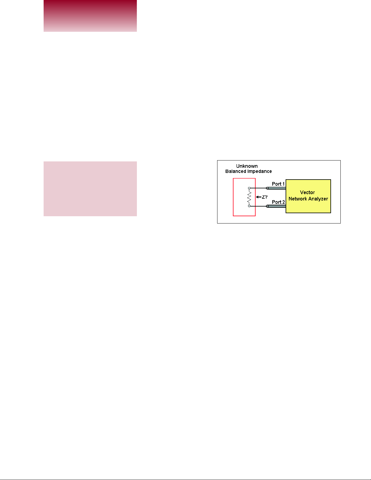
Figure 1 illustrates the test configuration
for measuring a balanced impedance with an
unbalanced VNA. The differential port or balanced impedance to be measured has two
nodes above ground potential. The procedure
is to apply each unbalanced port from the
VNA to one side of the balanced port or
impedance. The VNA is then calibrated to the
point of contact with the circuit or the VNA’s
This article describes a
software-based method
for obtaining differential
measurements using a
two-port unbalanced
vector network analyzer
Figure 1 · Test configuration for making balanced measurements with an unbalanced
vector network analyzer.
From November 2003 High Frequency Electronics
Copyright © 2003 Summit Technical Media, LLC

56 High Frequency Electronics
High Frequency Products
DIFFERENTIAL MEASUREMENTS
port extensions (or electrical delay feature) is used. Then,
the full two-port S-parameter measurement is taken over
the frequency range of interest (yielding four complex S
parameters per frequency point). This data is then stored
on floppy disk and transferred to a computer running the
LINC2 program. LINC2 then transforms the VNA’s Sparameter data into differential impedance data and displays it in a number of different formats. The data can be
displayed as a linear differential reflection coefficient, a
differential return loss in dB or as a complex differential
impedance with real and imaginary parts.
Design Example—IF SAW Filter Matching
The receiver section of a CDMA cellular telephone,
recently designed by the author, employed an IF SAW filter that required at least one port (two terminals) to be
operated in a balanced configuration. The source and load
circuits that would connect to the SAW filter were ultimately single ended, so a matching BALUN needed to be
designed for one side of the filter. It was decided that a
matching BALUN would provide the balanced load at the
output side while the input side of the SAW filter would
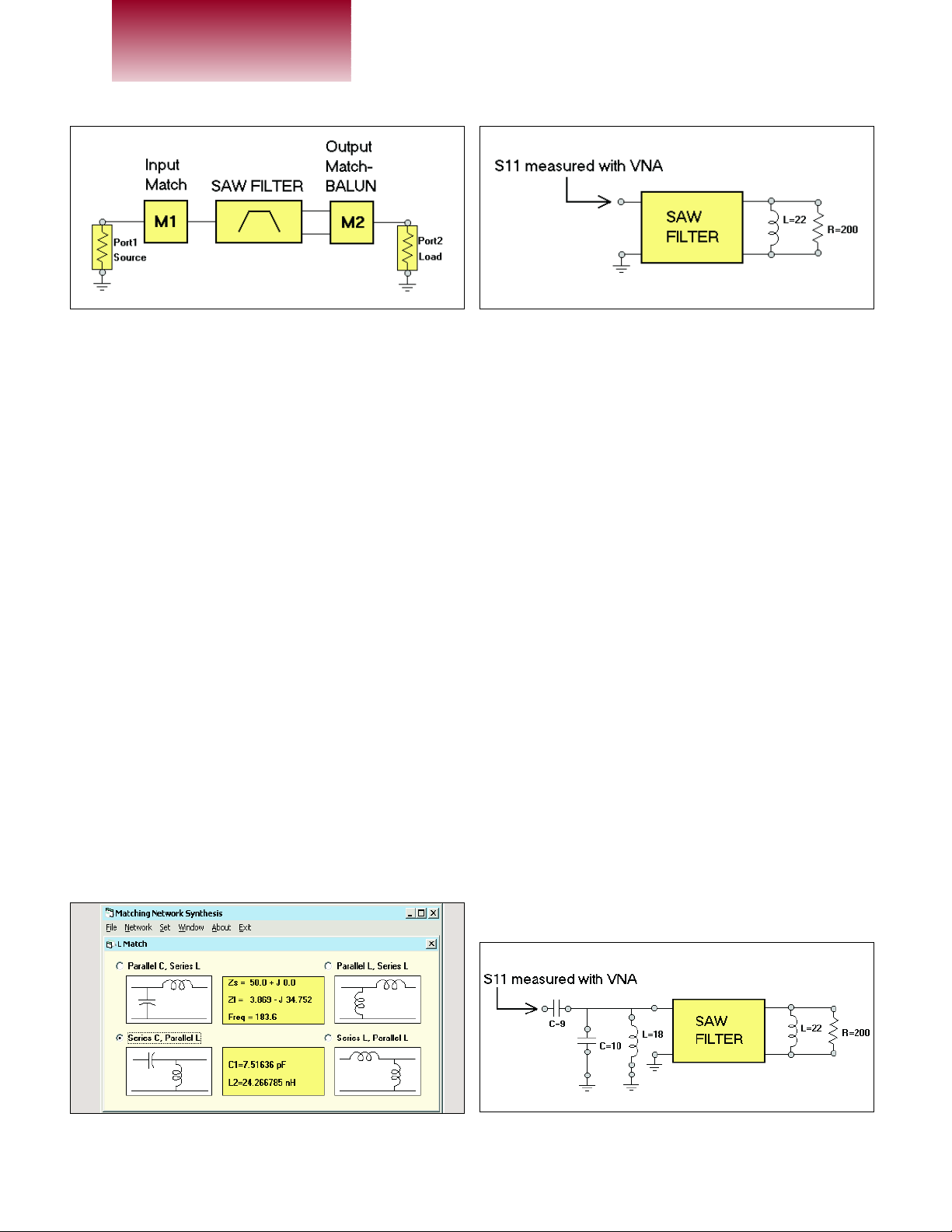
be matched with a single ended L match as shown in
Figure 2.
Note that the output BALUN (M2) we are talking
about here is part of the circuit and not a measurement
device. The following procedure was used to design the
input and output matching networks, M1 and M2:
Step 1—Determine the input impedance:
The input impedance of the SAW filter is determined
by terminating the output terminals of the filter with the
manufacturer’s specified load impedance and then measuring the single-ended input impedance with a Vector
Network Analyzer. The load impedance specified on the
data sheet is only an approximation because it doesn’t
take into account the parasitic effects of the layout for the
application circuit. However, any moderate amount of
mismatch at the output will hardly be seen at the input
because of the isolation provided by the filter’s 10 dB of
insertion loss. The manufacturer’s data sheet for the
CDMA SAW filter in Figure 2 calls for 200 ohms in parallel with a 23 nH inductor. The nearest standard value of
22 nH was used for the load inductor while the input
reflection coefficient (S
11
) was measured with a VNA as
shown in Figure 3.
The measured S
11
indicated an input impedance of
3.869 –j34.752 ohms.
Step 2—Design the input match:
Designing the matching network is easy with LINC2.
Simply select the desired type of network from a list in
the impedance matching tool and enter the source
impedance (50 ohms), load impedance (3.869 –j34.752
ohms) and the operating frequency (183.6 MHz). LINC2’s
“Network” menu contains various forms of lumped and
distributed (transmission line) matching networks. The L
network was chosen for this example.
From the given impedance data, LINC2 computes all
Figure 2 · SAW filter example.
Figure 4 · Input matching network options. Figure 5 · Final input match after tuning.
Figure 3 · Step 1: Input impedance measurement.
 Loading...