Analog Devices AD684 Datasheet

Four-Channel
a
FEATURES
Four Matched Sample-and-Hold Amplifiers
Independent Inputs, Outputs and Control Pins
500 ns Hold Mode Settling
1 ms Maximum Acquisition Time to 0.01%
Low Droop Rate: 0.01 mV/ms
Internal Hold Capacitors
75 ps Maximum Aperture Jitter
Low Power Dissipation: 430 mW
0.3" Skinny DIP Package
MIL-STD-883 Compliant Versions Available
PRODUCT DESCRIPTION
The AD684 is a monolithic quad sample-and-hold amplifier
(SHA). It features four complete sampling channels, each
controlled by an independent hold command. Each SHA is
complete with an internal hold capacitor. The high accuracy
SHA channels are self-contained and require no external
components or adjustments. The AD684 is manufactured on a
BiMOS process which provides a merger of high performance
bipolar circuitry and low power CMOS logic.
The AD684 is ideal for high performance, multichannel data
acquisition systems. Each SHA channel can acquire a signal in
less than 1 µs and retain the held value with a droop rate of less
than 0.01 µV/µs. Excellent linearity and ac performance make
the AD684 an ideal front end for high speed 12- and 14-bit
ADCs.
The AD684 has a self-correcting architecture that minimizes
hold mode errors and insures accuracy over temperature. Each
channel of the AD684 is capable of sourcing 5 mA and
incorporates output short circuit protection.
The AD684 is specified for three temperature ranges. The J
grade device is specified for operation from 0 to +70°C, the A
grade from –40°C to +85°C and the S grade from –55°C to
+125°C.
Sample-and-Hold Amplifier
AD684*
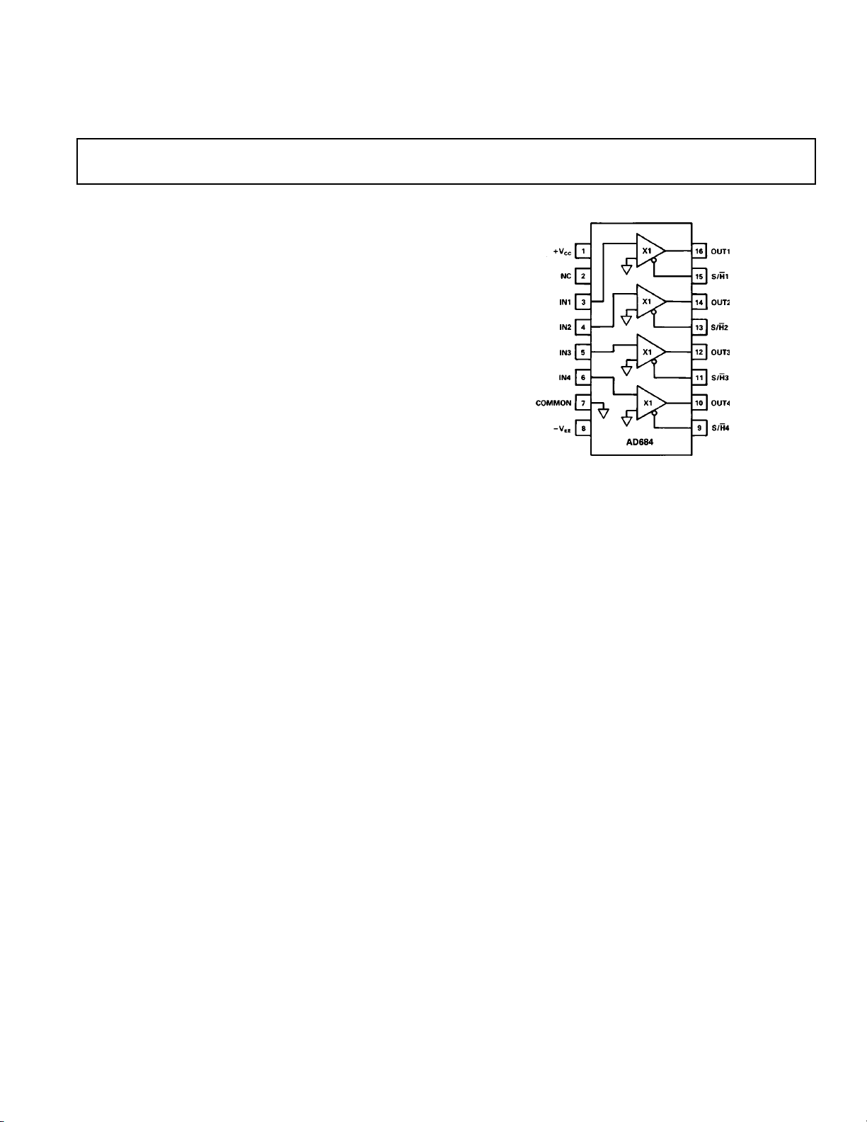
FUNCTIONAL BLOCK DIAGRAM
PRODUCT HIGHLIGHTS
1. Fast acquisition time (1 µs) and low aperture jitter (75 ps)
make the AD684 the best choice for multiple channel data
acquisition systems.
2. Monolithic construction insures excellent interchannel
matching in terms of timing and accuracy, as well as high
reliability.
3. Independent inputs, outputs and sample-and-hold controls
allow user flexibility in system architecture.
4. Low droop (0.01 µV/µs) and internally compensated hold
mode error results in superior system accuracy.
5. The AD684’s fast settling time and low output impedance
make it ideal for driving high speed analog to digital
converters such as the AD578, AD674, AD7572 and the
AD7672.
6. The AD684 is available in versions compliant with MILSTD-883. Refer to the Analog Devices Military Products
Databook or current AD684/883B data sheet for detailed
specifications.
*Protected by U.S. Patent Number 4,962,325.
REV. A
Information furnished by Analog Devices is believed to be accurate and
reliable. However, no responsibility is assumed by Analog Devices for its
use, nor for any infringements of patents or other rights of third parties
which may result from its use. No license is granted by implication or
otherwise under any patent or patent rights of Analog Devices.
One Technology Way, P.O. Box 9106, Norwood, MA 02062-9106, U.S.A.
Tel: 617/329-4700 Fax: 617/326-8703

AD684–SPECIFICATIONS
(T
to T
MIN
with VCC = +12 V 6 10%, V
MAX
= –12 V 6 10%, unless otherwise noted)
EE
Parameter Min Typ Max Min Typ Max Min Typ Max Units
AD684J AD684A AD684S
SAMPLING CHARACTERISTICS
Acquisition Time
10 V Step to 0.01% 0.75 1.0 0.75 1.0 0.75 1.0 µs
10 V Step to 0.1% 0.5 0.6 0.5 0.6 0.5 0.6 µs
Small Signal Bandwidth 4 4 4 MHz
Full Power Bandwidth 1 1 1 MHz
HOLD CHARACTERISTICS
Effective Aperture Delay –35 –25 –15 –35 –25 –15 –35 –25 –15 ns
Aperture Jitter 50 75 50 75 50 75 ps
Hold Settling Time (to 1 mV) 250 500 250 500 250 500 ns
Droop Rate
l
0.01 1 0.01 1 0.01 1 µV/µs
Feedthrough
(VIN = ± 5 V, 100 kHz) –90 –90 –90 dB
ACCURACY CHARACTERISTICS
1
Hold Mode Offset –4 –1 +3 –4 1 +3 –4 –1 +3 mV
Hold Mode Offset Drift 10 10 10 µV/°C
Sample Mode Offset 50 200 50 200 50 200 mV
Nonlinearity ±0.002 ±0.003 ±0.002 ±0.003 ±0.003 ±0.005 % FS
Gain Error ±0.03 60.05 ±0.03 60.05 ± 0.03 60.05 % FS
INTERCHANNEL CHARACTERISTICS
Interchannel Isolation
(V
= ± 5 V, 100 kHz) 80 86 80 86 80 86 dB
IN
Interchannel Aperture Offset 150 300 150 300 150 300 ps
Interchannel Offset 0.4 1.5 0.4 2.0 0.4 2.0 mV
OUTPUT CHARACTERISTICS
Output Drive Current
2
–5 +5 –5 +5 –5 +5 mA
Output Resistance, dc 0.3 0.5 0.3 0.5 0.3 0.5 Ω
Total Output Noise
(dc to 5 MHz) 150 150 150 µV rms
Sampled dc Uncertainty 85 85 85 µV rms
Hold Mode Noise
(dc to 5 MHz) 125 125 125 µV rms
Short Circuit Current
3
Source 20 20 20 mA
Sink 10 10 10 mA
INPUT CHARACTERISTICS
Input Voltage Range –5 +5 –5 +5 –5 +5 V
Bias Current
4
100 250 100 250 100 250 nA
400 500 500 nA
Input Impedance 50 50 50 MΩ
Input Capacitance 2 2 2 pF
DIGITAL CHARACTERISTICS
Input Voltage Low 0.8 0.8 0.8 V
Input Voltage High 2.0 2.0 2.0 V
Input Current (V
= 5 V) 2 10 2 10 2 10 µA
IN
POWER SUPPLY CHARACTERISTICS
Operating Voltage Range (V
, VEE) ±10.8 ±12 ±13.2 ± 10.8 ±12 ±13.2 ±10.8 ±12 ±13.2 V
CC
Supply Current 18 25 18 25 18 26 mA
+PSRR 65 70 65 70 65 70 dB
–PSRR 60 65 60 65 60 65 dB
Power Consumption 430 600 430 600 430 625 mW
TEMPERATURE RANGE
Specified Performance 0 +70 –40 +85 –55 +125 °C
PACKAGE OPTIONS
16-Pin Cerdip (Q) AD684JQ AD684AQ AD684SQ
NOTES
1
Specified and tested over an input range of ±5 V.
2
Maximum current the AD684 can source (or sink). Testing guarantees that the accuracy of the held signal remains within 2.5 mV of its initial value.
3
The output is protected for a short circuit to common, VCC and VEE .
4
VCC and VEE at nominal voltage levels.
Specifications shown in boldface are tested on all production units at final electrical test. Results from those tests are used to calculate outgoing quality levels. All min and max
specifications are guaranteed, although only those shown in boldface are tested on all production units.
Specifications subject to change without notice.
–2–
REV. A

ABSOLUTE MAXIMUM RATINGS*
With
Spec Respect to Min Max Unit
AD684
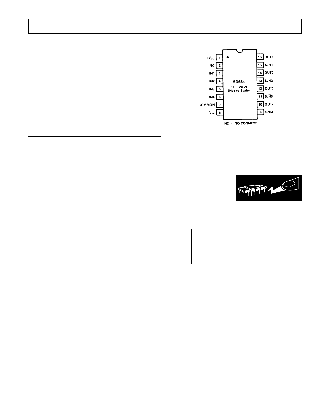
PIN CONFIGURATION
V
CC
V
EE
Common –0.3 +15 V
Common –15 +0.3 V
Control Inputs Common –0.5 +7 V
Analog Inputs Common –12 +12 V
Output Short Circuit to
Ground, V
CC
or V
EE
Indefinite
Max Junction
Temperature +175 °C
Storage –65 +150 °C
Lead Temperature
(10 sec max) +300 °C
Power Dissipation 640 mW
*Stresses above those listed under “Absolute Maximum Ratings” may cause
permanent damage to the device. This is a stress rating only and functional
operation of the device at these or any other conditions above those indicated in the
operational section of this specification is not implied.
CAUTION
ESD (electrostatic discharge) sensitive device. Electrostatic charges as high as 4000 V readily
accumulate on the human body and test equipment and can discharge without detection.
Although the AD684 features proprietary ESD protection circuitry, permanent damage may
occur on devices subjected to high energy electrostatic discharges. Therefore, proper ESD
precautions are recommended to avoid performance degradation or loss of functionality.
WARNING!
ESD SENSITIVE DEVICE
ORDERING GUIDE
Package
2
Model
1
Temperature Range Option
AD684JQ 0 to +70°C Q-16
AD684AQ –40°C to +85°C Q-16
AD684SQ –55°C to +125°C Q-16
NOTES
1
For details on grade and package offerings screened in accordance
with MIL-STD-883, refer to the Analog Devices Military Products Databook or current AD684/883B data sheet.
2
Q = Cerdip.
REV. A
–3–
 Loading...