250 MHz Bandwidth
–
FEATURES
SNR = 65.8 dBFS at fIN up to 250 MHz at 500 MSPS
ENOB of 10.5 bits at f
SFDR = 80 dBc at f
Excellent linearity
DNL = ±0.5 LSB typical, INL = ±0.6 LSB typical
Integrated 16k × 12 FIFO
FIFO readback options
12-bit parallel CMOS at 62.5 MHz
6-bit DDR LVDS interface
SPORT at 62.5 MHz
SPI at 25 MHz
High speed synchronization capability
1 GHz full power analog bandwidth
Integrated input buffer
On-chip reference, no external decoupling required
Low power dissipation
695 mW at 500 MSPS
Programmable input voltage range
1.18 V to 1.6 V, 1.5 V nominal
1.9 V analog and digital supply operation
1.9 V or 3.3 V SPI and SPORT operation
Clock duty cycle stabilizer
Integrated data clock output with programmable clock and
data alignment
up to 250 MHz at 500 MSPS (−1.0 dBFS)
IN
up to 250 MHz at 500 MSPS (−1.0 dBFS)
IN
DPD Observation Receiver
AD6641
GENERAL DESCRIPTION
The AD6641 is a 250 MHz bandwidth digital predistortion
(DPD) observation receiver that integrates a 12-bit 500 MSPS
ADC, a 16k × 12 FIFO, and a multimode back end that allows
users to retrieve the data through a serial port (SPORT), the SPI
interface, a 12-bit parallel CMOS port, or a 6-bit DDR LVDS
port after being stored in the integrated FIFO memory. It is optimized for outstanding dynamic performance and low power
consumption and is suitable for use in telecommunications
applications such as a digital predistortion observation path
where wider bandwidths are desired. All necessary functions,
including the sample-and-hold and voltage reference, are
included on the chip to provide a complete signal conversion
solution.
The on-chip FIFO allows small snapshots of time to be captured
via the ADC and read back at a lower rate. This reduces the
constraints of signal processing by transferring the captured
data at an arbitrary time and at a much lower sample rate. The
FIFO can be operated in several user-programmable modes. In
the single capture mode, the ADC data is captured when signaled via the SPI port or the use of the external FILL± pins. In
the continuous capture mode, the data is loaded continuously
into the FIFO and the FILL± pins are used to stop this operation.
APPLICATIONS
Wireless and wired broadband communications
Communications test equipment
Power amplifier linearization
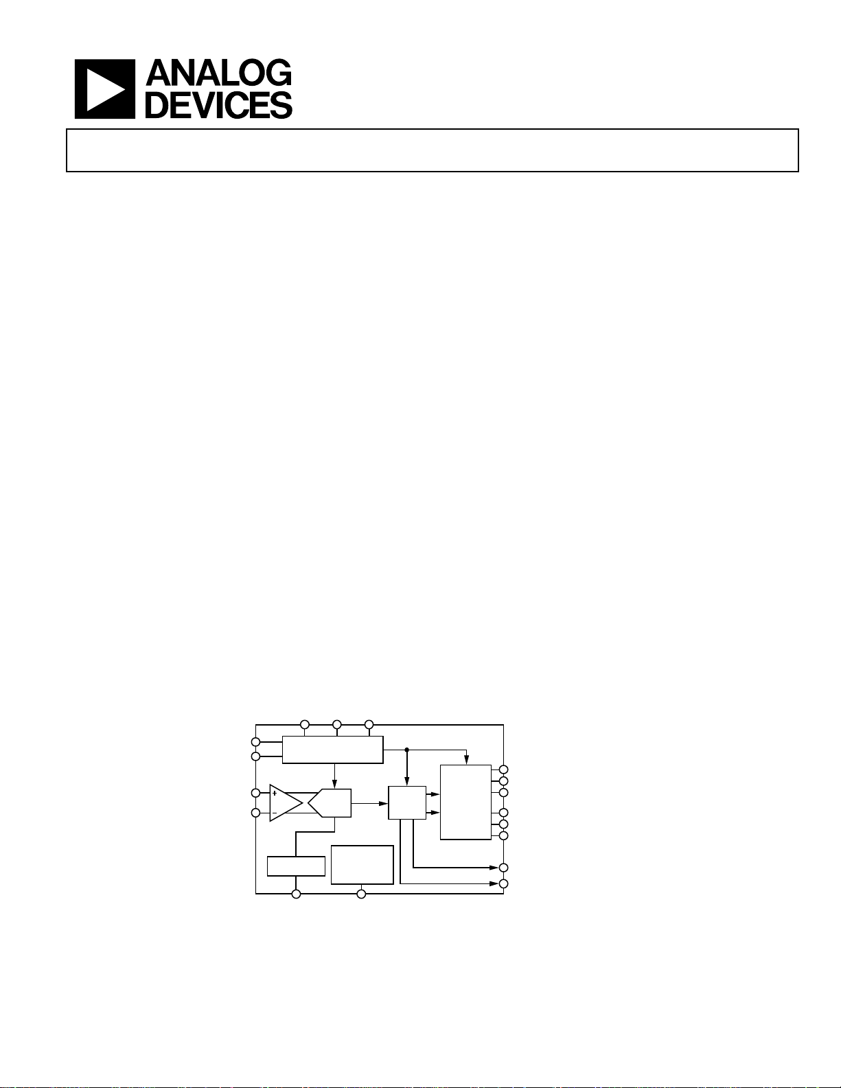
FUNCTIONAL BLOCK DIAGRAM
DUMPFILL+ FILL
CLK+
CLK–
VIN+
VIN–
Rev. 0
Information furnished by Analog Devices is believed to be accurate and reliable. However, no
responsibility is assumed by Anal og Devices for its use, nor for any infringements of patents or ot her
rights of third parties that may result from its use. Specifications subject to change without notice. No
license is granted by implication or otherwise under any patent or patent rights of Analog Devices.
Trademarks and registered trademarks are the property of their respective owners.
CLOCK AND CONTROL
ADC
REFERENCE
VREF
SPI CONTROL
SCLK, SDIO, AND CSB
AND DATA
FIFO
16k × 12
PCLK+
PARALLEL
AND
SPORT
OUTPUTS
Figure 1.
One Technology Way, P.O. Box 9106, Norwood, MA 02062-9106, U.S.A.
Tel: 781.329.4700 www.analog.com
Fax: 781.461.3113 ©2011 Analog Devices, Inc. All rights reserved.
PCLK–
PD[5:0]± IN DDR LVDS MODE
OR PD[11:0] IN CMOS MODE
SP_SCLK
SP_SDFS
SP_SDO
FULL
EMPTY
09813-001

AD6641
TABLE OF CONTENTS
Features.............................................................................................. 1
Applications....................................................................................... 1
General Description ......................................................................... 1
Functional Block Diagram .............................................................. 1
Revision History ............................................................................... 2
Product Highlights ........................................................................... 3
Specifications..................................................................................... 4
DC Specifications ......................................................................... 4
AC Specifications.......................................................................... 5
Digital Specifications ................................................................... 6
Switching Specifications.............................................................. 7
SPI Timing Requirements ........................................................... 8
Absolute Maximum Ratings.......................................................... 10
REVISION HISTORY
4/11—Revision 0: Initial Version
Thermal Resistance.................................................................... 10
ESD Caution................................................................................ 10
Pin Configurations and Function Descriptions......................... 11
Typical Performance Characteristics........................................... 15
Equivalent Circuits......................................................................... 18
SPI Register Map ............................................................................ 20
Theory of Operation ...................................................................... 23
FIFO Operation.......................................................................... 23
FIFO Output Interfaces ............................................................. 26
Configuration Using the SPI..................................................... 27
Outline Dimensions....................................................................... 28
Ordering Guide .......................................................................... 28
Rev. 0 | Page 2 of 28

AD6641
The data stored in the FIFO can be read back based on several
user-selectable output modes. The DUMP pin can be asserted
to output the FIFO data. The data stored in the FIFO can be
accessed via a SPORT, SPI, 12-bit parallel CMOS port, or 6-bit
DDR LVDS interface. The maximum output throughput
supported by the AD6641 is in the 12-bit CMOS or 6-bit DDR
LVDS mode and is internally limited to 1/8
input sample rate. This corresponds to the maximum output
data rate of 62.5 MHz at an input clock rate of 500 MSPS.
The ADC requires a 1.9 V analog voltage supply and a differential clock for full performance operation. Output format options
include twos complement, offset binary format, or Gray code. A
data clock output is available for proper output data timing. Fabricated on an advanced SiGe BiCMOS process, the device is
available in a 56-lead LFCSP and is specified over the industrial
temperature range (−40°C to +85°C). This product is protected
by a U.S. patent.
th
of the maximum
PRODUCT HIGHLIGHTS
1. High Performance ADC Core.
Maintains 65.8 dBFS SNR at 500 MSPS with a 250 MHz input.
2. Low Power.
Consumes only 695 mW at 500 MSPS.
3. Ease of Use.
On-chip 16k FIFO allows the user to target the high performance ADC to the time period of interest and reduce the
constraints of processing the data by transferring it at an
arbitrary time and a lower sample rate. The on-chip reference and sample-and-hold provide flexibility in system
design. Use of a single 1.9 V supply simplifies system power
supply design.
4. Serial Port Control.
Standard serial port interface supports configuration of the
device and customization for the user’s needs.
5. 1.9 V or 3.3 V SPI and Serial Data Port Operation.
Rev. 0 | Page 3 of 28

AD6641
SPECIFICATIONS
DC SPECIFICATIONS
AVDD = 1.9 V, DRVDD = 1.9 V, T
Table 1.
AD6641-500
Parameter1 Temp Min Typ Max Unit
RESOLUTION 12 Bits
ACCURACY
No Missing Codes Full Guaranteed
Offset Error Full −2.6 0.0 +1.8 mV
Gain Error Full −6.8 −2.3 +3.3 % FS
Differential Nonlinearity (DNL) Full ±0.5 LSB
Integral Nonlinearity (INL) Full ±0.6 LSB
TEMPERATURE DRIFT
Offset Error Full 18 μV/°C
Gain Error Full 0.07 %/°C
ANALOG INPUTS (VIN±)
Differential Input Voltage Range2 Full 1.18 1.5 1.6 V p-p
Input Common-Mode Voltage Full 1.8 V
Input Resistance (Differential) Full 1 kΩ
Input Capacitance (Differential) 25°C 1.3 pF
POWER SUPPLY
AVDD Full 1.8 1.9 2.0 V
DRVDD Full 1.8 1.9 2.0 V
SPI_VDDIO Full 1.8 1.9 3.3 V
Supply Currents
3
I
Full 300 330 mA
AVDD
3
I
Full 66 80 mA
DRVDD
Power Dissipation3 Full 695 779 mW
Power-Down Dissipation Full 15 mW
Standby Dissipation Full 72 mW
Standby to Power-Up Time Full 10 μs
1
See the AN-835 Application Note, Understanding High Speed ADC Testing and Evaluation, for a complete set of definitions and information about how these tests were
completed.
2
The input range is programmable through the SPI, and the range specified reflects the nominal values of each setting. See the SPI Register Map section for additional
details.
3
I
AVDD
and I
are measured with a −1 dBFS, 30 MHz sine input at a rated sample rate.
DRVDD
= −40°C, T
MIN
= +85°C, fIN = −1.0 dBFS, full scale = 1.5 V, unless otherwise noted.
MAX
Rev. 0 | Page 4 of 28

AD6641
AC SPECIFICATIONS
AVDD = 1.9 V, DRVDD = 1.9 V, T
Table 2.
AD6641-500
Parameter
1, 2
Temp Min Typ Max Unit
SNR
fIN = 30 MHz 25°C 66.0 dBFS
fIN = 125 MHz 25°C 65.9 dBFS
Full 65.0 dBFS
fIN = 250 MHz 25°C 65.8 dBFS
fIN = 450 MHz 25°C 65.1 dBFS
SINAD
fIN = 30 MHz 25°C 66.0 dBFS
fIN = 125 MHz 25°C 65.7 dBFS
Full 63.8 dBFS
fIN = 250 MHz 25°C 65.3 dBFS
fIN = 450 MHz 25°C 64.6 dBFS
EFFECTIVE NUMBER OF BITS (ENOB)
fIN = 30 MHz 25°C 10.7 Bits
fIN = 125 MHz 25°C 10.6 Bits
fIN = 250 MHz 25°C 10.5 Bits
fIN = 450 MHz 25°C 10.4 Bits
SFDR
fIN = 30 MHz 25°C 88 dBc
fIN = 125 MHz 25°C 83 dBc
Full 77 dBc
fIN = 250 MHz 25°C 80 dBc
fIN = 450 MHz 25°C 72 dBc
WORST HARMONIC (SECOND OR THIRD)
fIN = 30 MHz 25°C −92 dBc
fIN = 125 MHz 25°C −77 dBc
Full −84 dBc
fIN = 250 MHz 25°C −80 dBc
fIN = 450 MHz 25°C −72 dBc
WORST OTHER HARMONIC (SFDR EXCLUDING SECOND AND THIRD)
fIN = 30 MHz 25°C −90 dBc
fIN = 125 MHz 25°C −90 dBc
Full −77 dBc
fIN = 250 MHz 25°C −85 dBc
fIN = 450 MHz 25°C −78 dBc
TWO-TONE IMD
f
= 119.8 MHz, f
IN1
= 125.8 MHz (−7 dBFS, Each Tone) 25°C −82 dBc
IN2
ANALOG INPUT BANDWIDTH 25°C 1 GHz
1
All ac specifications tested by driving CLK+ and CLK− differentially.
2
See the AN-835 Application Note, Understanding High Speed ADC Testing and Evaluation, for a complete set of definitions and information about how these tests were
completed.
= −40°C, T
MIN
= +85°C, fIN = −1.0 dBFS, full scale = 1.5 V, unless otherwise noted.
MAX
Rev. 0 | Page 5 of 28

AD6641
DIGITAL SPECIFICATIONS
AVDD = 1.9 V, DRVDD = 1.9 V, T
Table 3.
AD6641-500
Parameter1 Temp Min Typ Max Unit
CLOCK INPUTS (CLK±)
Logic Compliance Full CMOS/LVDS/LVPECL
Internal Common-Mode Bias Full 0.9 V
Differential Input Voltage
High Level Input (VIH) Full 0.2 1.8 V p-p
Low Level Input (VIL) Full −1.8 −0.2 V p-p
High Level Input Current (IIH) Full −10 +10 μA
Low Level Input Current (IIL) Full −10 +10 μA
Input Resistance (Differential) Full 8 10 12 kΩ
Input Capacitance Full 4 pF
LOGIC INPUTS (SPI, SPORT)
Logic Compliance Full CMOS
Logic 1 Voltage Full 0.8 × SPI_VDDIO V
Logic 0 Voltage Full 0.2 × SPI_VDDIO V
Logic 1 Input Current (SDIO) Full 0 μA
Logic 0 Input Current (SDIO) Full −60 μA
Logic 1 Input Current (SCLK) Full 50 μA
Logic 0 Input Current (SCLK) Full 0 μA
Input Capacitance 25°C 4 pF
LOGIC INPUTS (DUMP, CSB)
Logic Compliance Full CMOS
Logic 1 Voltage Full 0.8 × DRVDD V
Logic 0 Voltage Full 0.2 × DRVDD V
Logic 1 Input Current Full 0 μA
Logic 0 Input Current Full −60 μA
Input Capacitance 25°C 4 pF
LOGIC INPUTS (FILL±)
Logic Compliance Full CMOS/LVDS/LVPECL
Internal Common-Mode Bias Full 0.9 V
Differential Input Voltage
High Level Input (VIH) Full 0.2 1.8 V p-p
Low Level Input (VIL) Full −1.8 −0.2 V p-p
High Level Input Current (IIH) Full −10 +10 μA
Low Level Input Current (IIL) Full −10 +10 μA
Input Resistance (Differential) Full 8 10 12 kΩ
Input Capacitance Full 4 pF
LOGIC OUTPUTS2 (FULL, EMPTY)
Logic Compliance Full CMOS
High Level Output Voltage Full DRVDD − 0.05 V
Low Level Output Voltage Full DRGND + 0.05 V
LOGIC OUTPUTS2 (SPI, SPORT)
Logic Compliance Full CMOS
High Level Output Voltage Full SPI_VDDIO − 0.05 V
Low Level Output Voltage Full DRGND + 0.05 V
= −40°C, T
MIN
= +85°C, fIN = −1.0 dBFS, full scale = 1.5 V, unless otherwise noted.
MAX
Rev. 0 | Page 6 of 28

AD6641
AD6641-500
Parameter1 Temp Min Typ Max Unit
LOGIC OUTPUTS
DDR LVDS Mode (PCLK±, PD[5:0]±, PDOR±)
Logic Compliance Full LVDS
VOD Differential Output Voltage Full 247 454 mV
VOS Output Offset Voltage Full 1.125 1.375 V
Parallel CMOS Mode (PCLK±, PD[11:0])
Logic Compliance Full CMOS
High Level Output Voltage Full DRVDD − 0.05 V
Low Level Output Voltage Full DRGND + 0.05 V
Output Coding Twos complement, Gray code, or offset binary (default)
1
See the AN-835 Application Note, Understanding High Speed ADC Testing and Evaluation, for a complete set of definitions and information about how these tests were
completed.
2
5 pF loading.
SWITCHING SPECIFICATIONS
AVDD = 1.9 V, DRVDD = 1.9 V, T
Table 4.
AD6641-500
Parameter1 Temp Min Typ Max Unit
OUTPUT DATA RATE
Maximum Output Data Rate (Decimate by 8 at 500 MSPS Sample Rate, Parallel CMOS
or DDR LVDS Mode Interface)
Maximum Output Data Rate (Decimate by 8 at 500 MSPS Sample Rate, SPORT Mode) Full 62.5 MHz
PULSE WIDTH/PERIOD (CLK±)
CLK± Pulse Width High (tCH) Full 1 ns
CLK± Pulse Width Low (tCL) Full 1 ns
Rise Time (tR) (20% to 80%) 25°C 0.2 ns
Fall Time (tF) (20% to 80%) 25°C 0.2 ns
PULSE WIDTH/PERIOD (PCLK±, DDR LVDS MODE)
PCLK± Pulse Width High (t
PCLK± Period (t
PCLK
Propagation Delay (t
PCLK_CH
) Full 16 ns
, CLK± to PCLK±) Full ±0.1 ns
CPD
Rise Time (tR) (20% to 80%) 25°C 0.2 ns
Fall Time (tF) (20% to 80%) 25°C 0.2 ns
Data to PCLK Skew (t
) Full 0.2 ns
SKEW
SERIAL PORT OUTPUT TIMING2
SP_SDFS Propagation Delay (t
SP_SDO Propagation Delay (t
SERIAL PORT INPUT TIMING
SP_SDFS Setup Time (t
SP_SDFS Hold Time (t
) Full 2 ns
SSF
) Full 2 ns
HSF
FILL± INPUT TIMING
FILL± Setup Time (t
FILL± Hold Time (t
) Full 0.5 ns
Sfill
) Full 0.7 ns
Hfill
APERTURE DELAY (tA) 25°C 0.85 ns
APERTURE UNCERTAINTY (JITTER, tJ) 25°C 80 fs rms
1
See the AN-835 Application Note, Understanding High Speed ADC Testing and Evaluation, for a complete set of definitions and information about how these tests were
completed.
2
5 pF loading.
= −40°C, T
MIN
= +85°C, fIN = −1.0 dBFS, full scale = 1.5 V, unless otherwise noted.
MAX
Full 62.5 MHz
) Full 8 ns
) Full 3 ns
DSDFS
) Full 3 ns
DSDO
Rev. 0 | Page 7 of 28

AD6641
SPI TIMING REQUIREMENTS
Table 5.
Parameter Description Limit Unit
tDS Setup time between the data and the rising edge of SCLK 2 ns min
tDH Hold time between the data and the rising edge of SCLK 2 ns min
t
Period of the SCLK 40 ns min
CLK
tS Setup time between CSB and SCLK 2 ns min
tH Hold time between CSB and SCLK 2 ns min
t
SCLK pulse width high 10 ns min
HIGH
t
SCLK pulse width low 10 ns min
LOW
t
Time required for the SDIO pin to switch from an input to an output relative to the SCLK falling edge 10 ns min
EN_SDIO
t
Time required for the SDIO pin to switch from an output to an input relative to the SCLK rising edge 10 ns min
DIS_SDIO
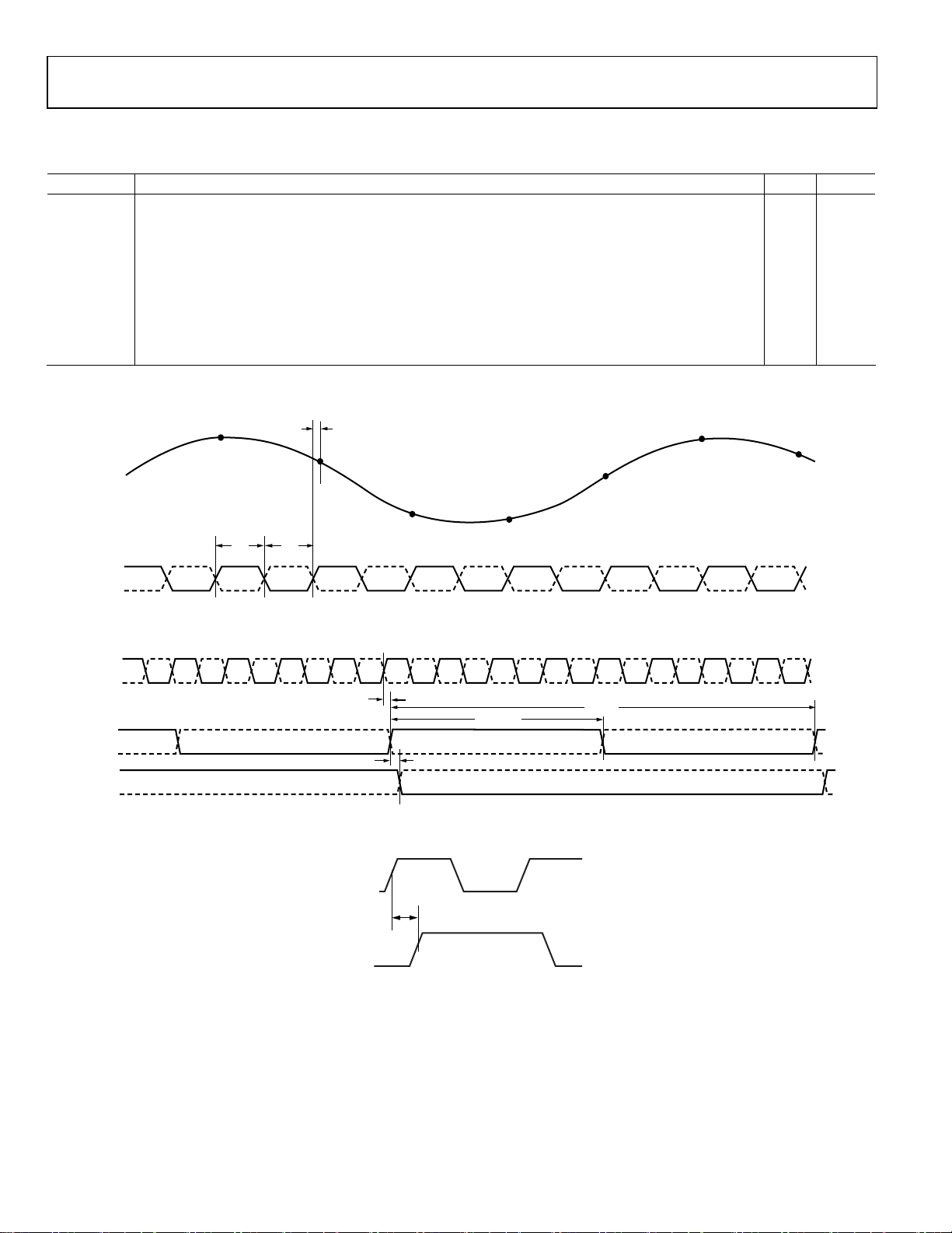
Timing Diagrams
VIN±
N–1
t
A
N
N+3
N+4
N+5
CLK+
CLK–
CLK+
CLK–
PCLK+
PCLK–
PD[11:0]
t
CH
OUTPUT DATA BUS
N+1
t
CL
Figure 2. Input Interface Timing
t
CPD
t
PCLK_CH
t
SKEW
Figure 3. Parallel CMOS Mode Output Interface Timing
SP_SCLK
t
DSDFS
SP_SDFS
Figure 4. SP_SDFS Propagation Delay
N+2
t
PCLK
09813-004
09813-002
09813-003
Rev. 0 | Page 8 of 28

AD6641
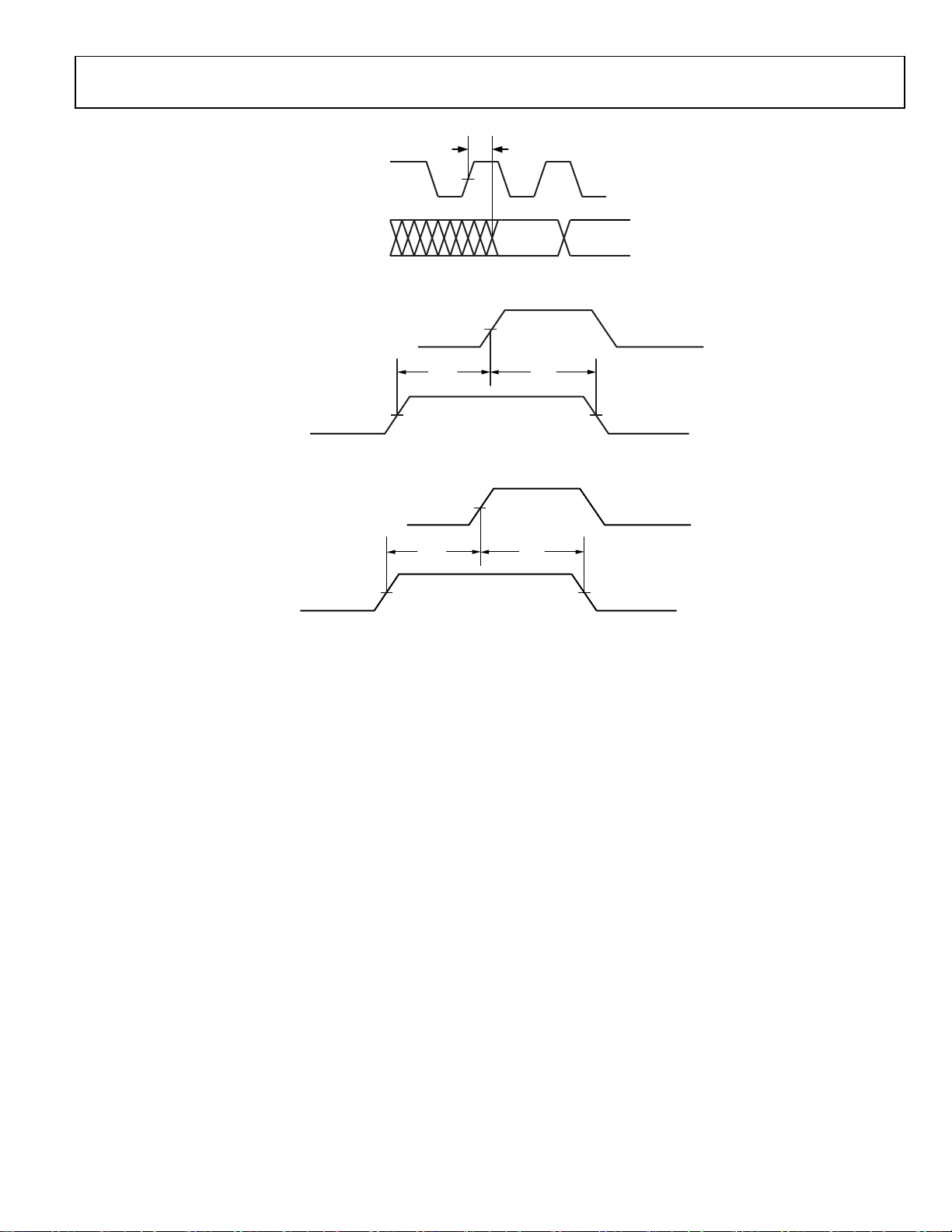
SP_SCLK
SP_SDO D11 D10
t
DSDO
09813-005
Figure 5. SP_SDO Propagation Delay
SP_SCLK
SP_SDFS
t
SSF
t
HSF
09813-006
Figure 6. Slave Mode SP_SDFS Setup/Hold Time
CLK±
t
Sfill
t
Hfill
FILL±
09813-007
Figure 7. FILL± Setup and Hold Times
Rev. 0 | Page 9 of 28
 Loading...