Analog Devices AD6640 Datasheet
12-Bit, 65 MSPS
a
FEATURES
65 MSPS Minimum Sample Rate
80 dB Spurious-Free Dynamic Range
IF-Sampling to 70 MHz
710 mW Power Dissipation
Single +5 V Supply
On-Chip T/H and Reference
Twos Complement Output Format
3.3 V or 5 V CMOS-Compatible Output Levels
APPLICATIONS
Cellular/PCS Base Stations
Multichannel, Multimode Receivers
GPS Anti-Jamming Receivers
Communications Receivers
Phased Array Receivers
PRODUCT DESCRIPTION
The AD6640 is a high speed, high performance, low power,
monolithic 12-bit analog-to-digital converter. All necessary
functions, including track-and-hold (T/H) and reference are
included on-chip to provide a complete conversion solution.
The AD6640 runs on a single +5 V supply and provides CMOScompatible digital outputs at 65 MSPS.
Specifically designed to address the needs of multichannel,
multimode receivers, the AD6640 maintains 80 dB spuriousfree dynamic range (SFDR) over a bandwidth of 25MHz.
Noise performance is also exceptional; typical signal-to-noise
ratio is 68 dB.
The AD6640 is built on Analog Devices’ high speed complementary bipolar process (XFCB) and uses an innovative multipass
architecture. Units are packaged in a 44-terminal Plastic Thin
Quad Flatpack (TQFP) specified from –40°C to +85°C.
IF Sampling A/D Converter
AD6640
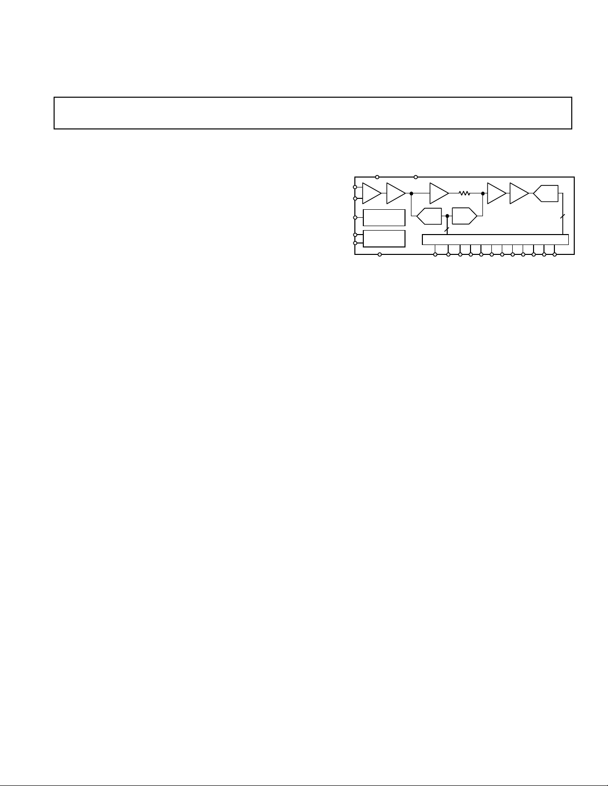
FUNCTIONAL BLOCK DIAGRAM
AV
AIN
BUF
AIN
V
REF
ENCODE
ENCODE
+2.4V
REFERENCE
INTERNAL
TIMING
GND
PRODUCT HIGHLIGHTS
1. Guaranteed sample rate is 65 MSPS.
2. Fully differential analog input stage specified for frequencies
up to 70 MHz; enables “IF Sampling.”
3. Low power dissipation: 710 mW off a single +5V supply.
4. Digital outputs may be run on +3.3 V supply for easy interface to digital ASICs.
5. Complete Solution: reference and track-and-hold.
6. Packaged in small, surface mount, plastic 44-terminal TQFP.
DV
CC
TH1
CC
A
TH2
DACADC
6
DIGITAL ERROR CORRECTION LOGIC
MSB
D11 D10 D9 D8 D7 D6 D5 D4 D3 D2 D1 D0
TH3
AD6640
ADC
7
LSB
REV. 0
Information furnished by Analog Devices is believed to be accurate and
reliable. However, no responsibility is assumed by Analog Devices for its
use, nor for any infringements of patents or other rights of third parties
which may result from its use. No license is granted by implication or
otherwise under any patent or patent rights of Analog Devices.
One Technology Way, P.O. Box 9106, Norwood, MA 02062-9106, U.S.A.
Tel: 781/329-4700 World Wide Web Site: http://www.analog.com
Fax: 781/326-8703 © Analog Devices, Inc., 1998
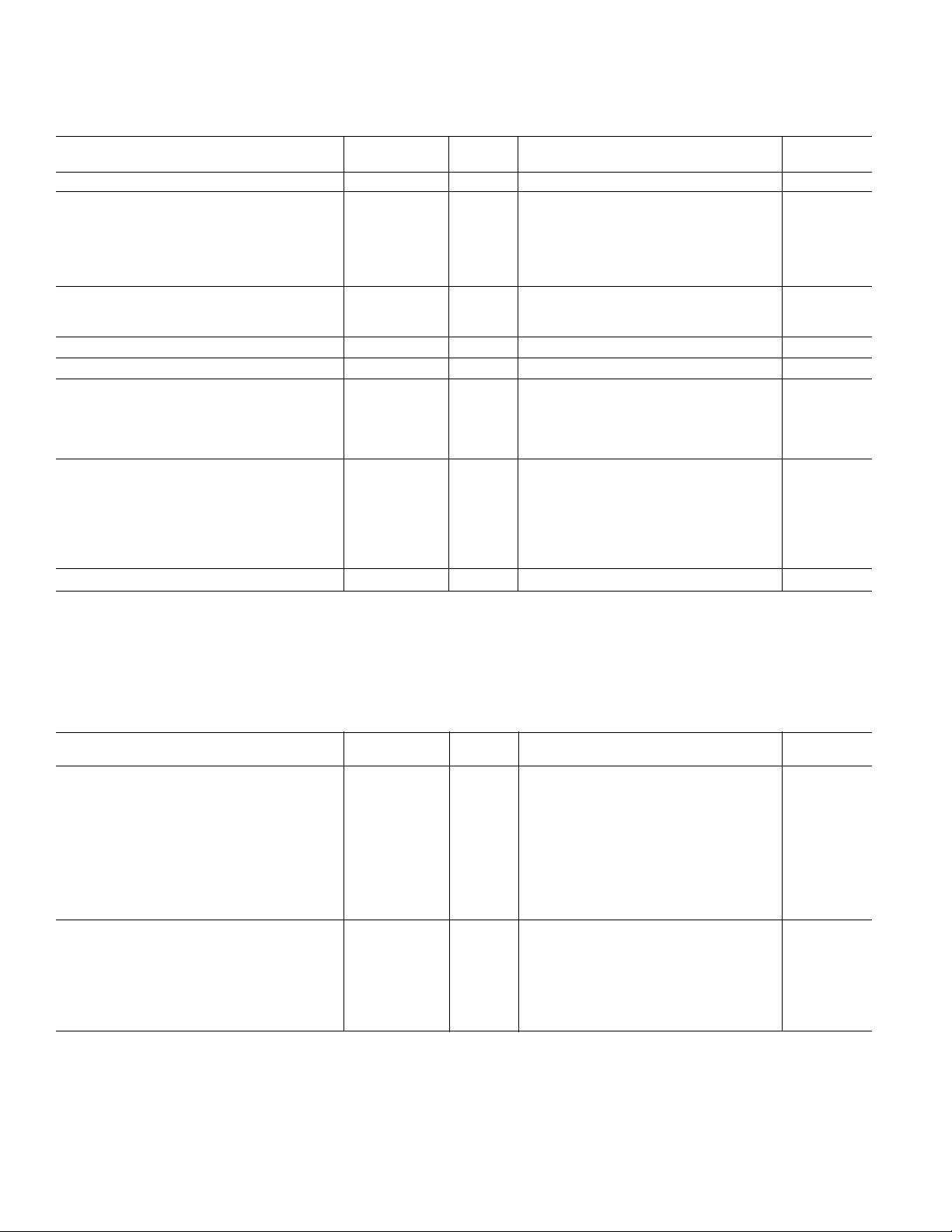
AD6640–SPECIFICA TIONS
DC SPECIFICATIONS
(AVCC = +5 V, DVCC = +3.3 V; T
= –408C, T
MIN
= +858C)
MAX
Test AD6640AST
Parameter Temp Level Min Typ Max Units
RESOLUTION 12 Bits
ACCURACY
No Missing Codes +25°C I GUARANTEED
Offset Error Full VI –10 3.5 +10 mV
Gain Error Full VI –10 4.0 +10 % FS
Differential Nonlinearity (DNL)
Integral Nonlinearity (INL)
1
1
+25°C I –1.0 ±0.5 +1.5 LSB
Full V ±1.25 LSB
TEMPERATURE DRIFT
Offset Error Full V 50 ppm/°C
Gain Error Full V 100 ppm/°C
POWER SUPPLY REJECTION (PSRR) Full V ±0.5 mV/V
REFERENCE OUT (V
ANALOG INPUTS (AIN, AIN)
Analog Input Common-Mode Range
REF
2
)
3
4
Full V 2.4 V
Full V V
± 0.05 V
REF
Differential Input Voltage Range Full V 2.0 V p-p
Differential Input Resistance Full IV 0.7 0.9 1.1 kΩ
Differential Input Capacitance +25°C V 1.5 pF
POWER SUPPLY
Supply Voltage
AV
DV
CC
CC
Full VI 4.75 5.0 5.25 V
Full VI 3.0 3.3 5.25 V
Supply Current
IA
(AVCC = 5.0 V) Full VI 135 160 mA
VCC
ID
(DVCC = 3.3 V) Full VI 10 20 mA
VCC
POWER CONSUMPTION Full VI 710 865 mW
NOTES
1
ENCODE = 20 MSPS
2
If V
is used to provide a dc offset to other circuits, it should first be buffered.
REF
3
The AD6640 is designed to be driven differentially. Both AIN and AIN should be driven at levels V
produce a 2 V p-p differential input signal. See Driving the Analog Inputs section for more details.
4
Analog input common-mode range specifies the offset range the analog inputs can tolerate in dc-coupled applications (see Figure 35 for more detail).
Specifications subject to change without notice
.
± 0.5 volts. The input signals should be 180 degrees out of phase to
REF
DIGITAL SPECIFICATIONS
(AVCC = +5 V, DVCC = +3.3 V; T
= –408C, T
MIN
= +858C)
MAX
Test AD6640AST
Parameter Temp Level Min Typ Max Units
LOGIC INPUTS (ENC, ENC)
Encode Input Common-Mode Range
1
2
Full IV 0.2 2.2 V
Differential Input Voltage Full IV 0.4 V p-p
Single-Ended Encode 10 V p-p
Logic Compatibility
3
TTL/CMOS
Logic “1” Voltage Full VI 2.0 5.0 V
Logic “0” Voltage Full VI 0 0.8 V
Logic “1” Current (V
Logic “0” Current (V
= 5 V) Full VI 500 650 800 µA
INH
= 0 V) Full VI –400 –320 –200 µA
INL
Input Capacitance +25°C V 2.5 pF
LOGIC OUTPUTS (D11–D0)
4
Logic Compatibility CMOS
Logic “1” Voltage (DV
Logic “0” Voltage (DV
Logic “1” Voltage (DV
Logic “0” Voltage (DV
= +3.3 V) Full VI 2.8 DVCC – 0.2 V
CC
= +3.3 V) Full VI 0.2 0.5 V
CC
= +5.0 V) Full IV 4.5 DVCC – 0.3 V
CC
= +5.0 V) Full IV 0.35 0.5 V
CC
Output Coding Twos Complement
NOTES
1
Best dynamic performance is obtained by driving ENC and ENC differentially. See Encoding the AD6640 section for more details. Performance versus ENC/ENC power is
shown in Figure 18 under Typical Performance Characteristics.
2
For dc-coupled applications, Encode Input Common-Mode Range specifies the common-mode range the encode inputs can tolerate when driven differentially by minimum
differential input voltage of 0.4 V p-p. For differential input voltage swings greater than 0.4 V p-p, the common-mode range will change. The minimum value insures that the
input voltage on either encode pin does not go below 0 V. The maximum value insures that the input voltage on either encode pin does not go below 2.0 V or above AVCC (e.g.,
for a differential input swing of 0.8 V, the min and max common-mode specs become 0.4 V and 2.4 V respectively).
3
ENC or ENC may be driven alone if desired, but performance will likely be degraded. Logic Compatibility specifications are provided to show that TTL or CMOS clock sources
will work. When driving only one encode input, bypass the complementary input to GND with 0.01 µF.
4
Digital output load is one LCX gate.
Specifications subject to change without notice.
–2–
REV. 0
AD6640
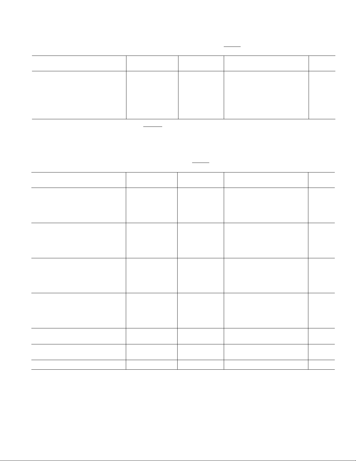
SWITCHING SPECIFICATIONS
1
(AVCC = +5 V, DVCC = +3.3 V; ENCODE & ENCODE = 65 MSPS; T
= –408C, T
MIN
= +858C)
MAX
Test AD6640AST
Parameter (Conditions) Temp Level Min Typ Max Units
Maximum Conversion Rate Full VI 65 MSPS
Minimum Conversion Rate
Aperture Delay (t
) +25°C V 400 ps
A
Aperture Uncertainty (Jitter) +25°C V 0.3 ps rms
ENCODE Pulsewidth High
ENCODE Pulsewidth Low +25°C IV 6.5 ns
Output Delay (tOD) DVCC +3.3 V/5.0 V
NOTES
1
All switching specifications tested by driving ENCODE and ENCODE differentially.
2
A plot of Performance vs. Encode is shown in Figure 16 under Typical Performance Characteristics.
3
A plot of Performance vs. Duty Cycle (Encode = 65 MSPS) is shown in Figure 17 under Typical Performance Characteristics.
4
Outputs driving one LCX gate. Delay is measured from differential crossing of ENC, ENC to the time when all output data bits are within valid logic levels.
Specifications subject to change without notice.
AC SPECIFICATIONS
2
3
4
1
(AVCC = +5 V, DVCC = +3.3 V; ENCODE & ENCODE = 65 MSPS; T
Full IV 6.5 MSPS
+25°C IV 6.5 ns
Full IV 8.5 10.5 12.5 ns
= –408C, T
MIN
= +858C)
MAX
Test AD6640AST
Parameter (Conditions) Temp Level Min Typ Max Units
SNR
Analog Input 2.2 MHz +25°CV 68 dB
@ –1 dBFS 15.5 MHz +25°C I 64 67.7 dB
31.0 MHz +25°C V 67.5 dB
69.0 MHz +25°CV 66 dB
SINAD
Analog Input 2.2 MHz +25°CV 68 dB
@ –1 dBFS 15.5 MHz +25°C I 63.5 67.2 dB
31.0 MHz +25°C V 67.0 dB
69.0 MHz +25°C V 65.5 dB
2
Worst Harmonic
(2nd or 3rd)
Analog Input 2.2 MHz +25°C V 80 dBc
@ –1 dBFS 15.5 MHz +25°C I 74 80 dBc
31.0 MHz +25°C V 79.5 dBc
69.0 MHz +25°C V 78.5 dBc
2
Worst Harmonic
(4th or Higher)
Analog Input 2.2 MHz +25°C V 85 dBc
@ –1 dBFS 15.5 MHz +25°C I 74 85 dBc
31.0 MHz +25°C V 85 dBc
69.0 MHz +25°C V 84 dBc
Multitone SFDR (w/Dither)
3
Eight Tones @ –20 dBFS Full V 90 dBFS
Two-Tone IMD Rejection
4
F1, F2 @ –7 dBFS Full V 80 dBc
Analog Input Bandwidth
NOTES
1
All ac specifications tested by driving ENCODE and ENCODE differentially.
2
For a single test tone at –1 dBFS, the worst case spectral performance is typically limited by the direct or aliased 2nd or 3rd harmonic. If a system is designed such
that the 2nd and 3rd harmonics fall out-of-band, overall performance in the band of interest is typically improved by 5 dB. Worst Harmonic (4th or Higher) includes
4th and higher order harmonics and all other spurious components. Reference Figure 12 for more detail.
3
See Overcoming Static Nonlinearities with Dither section for details on improving SFDR performance. To measure SFDR, eight tones from 14 MHz to 18 MHz
(0.5 MHz spacing) are swept from –20 dBFS to –90 dBFS. An open channel at 16 MHz is used to monitor SFDR.
4
F1 = 14.9 MHz, F2 = 16 MHz.
5
Specification is small signal bandwidth. Plots of Performance versus Analog Input Frequency are shown in Figures 10, 11 and 12. Sampling wide bandwidths
(5 MHz–15 MHz) should be limited to 70 MHz center frequency.
Specifications subject to change without notice.
5
+25°C V 300 MHz
REV. 0
–3–
AD6640
WARNING!
ESD SENSITIVE DEVICE
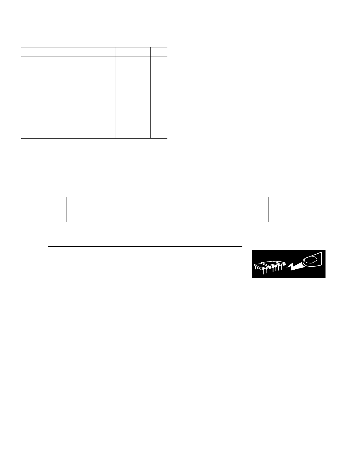
ABSOLUTE MAXIMUM RATINGS
Parameter Min Max Units
ELECTRICAL
AV
Voltage 0 7 V
CC
DV
Voltage 0 7 V
CC
Analog Input Voltage 0 AV
Analog Input Current 25 mA
Digital Input Voltage (ENCODE) 0 AV
Digital Output Current –10 10 mA
ENVIRONMENTAL
2
Operating Temperature Range
(Ambient) –40 +85 °C
Maximum Junction Temperature +150 °C
Lead Temperature (Soldering, 10 sec) +300 °C
Storage Temperature Range (Ambient) –65 +150 °C
NOTES
1
Absolute maximum ratings are limiting values to be applied individually, and
beyond which the serviceability of the circuit may be impaired. Functional
operability is not necessarily implied. Exposure to absolute maximum rating
conditions for an extended period of time may affect device reliability.
2
Typical thermal impedances (44-terminal TQFP); θJA = 55°C/W.
1
V
CC
V
CC
ORDERING GUIDE
EXPLANATION OF TEST LEVELS
Test Level
I – 100% production tested.
II – 100% production tested at +25°C, and sample tested at
specified temperatures. AC testing done on sample
basis.
III – Sample tested only.
IV – Parameter is guaranteed by design and characterization
testing.
V – Parameter is a typical value only.
VI – All devices are 100% production tested at +25°C; sample
tested at temperature extremes.
Model Temperature Range Package Description Package Option
AD6640AST –40°C to +85°C (Ambient) 44-Terminal TQFP (Thin Quad Plastic Flatpack) ST-44
AD6640ST/PCB Evaluation Board with AD6640AST
CAUTION
ESD (electrostatic discharge) sensitive device. Electrostatic charges as high as 4000 V readily
accumulate on the human body and test equipment and can discharge without detection.
Although the AD6640 features proprietary ESD protection circuitry, permanent damage may
occur on devices subjected to high energy electrostatic discharges. Therefore, proper ESD
precautions are recommended to avoid performance degradation or loss of functionality.
–4–
REV. 0
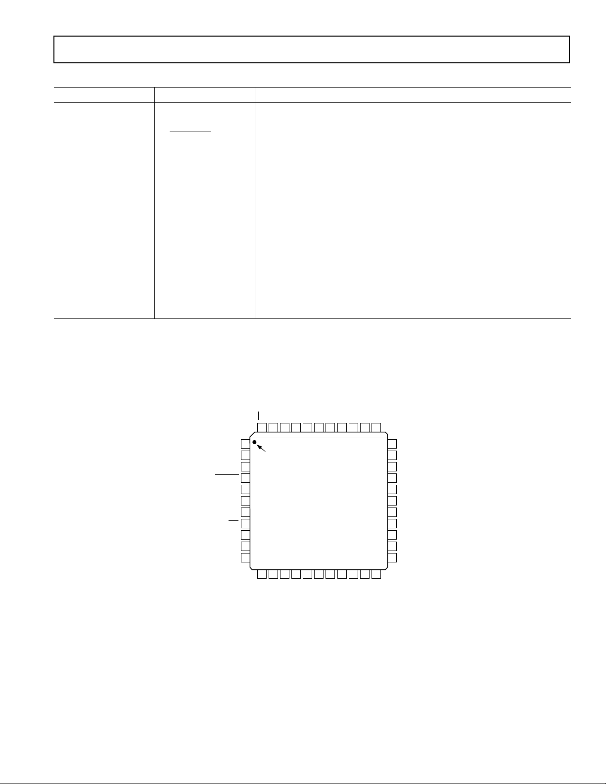
PIN FUNCTION DESCRIPTIONS
Pin No. Name Function
1, 2, 36, 37, 40, 41 DV
CC
+3.3 V/+5 V Power Supply (Digital). Powers output stage only.
3 ENCODE Encode Input. Data conversion initiated on rising edge.
4
ENCODE Complement of ENCODE. Drive differentially with ENCODE or bypass to
Ground for single-ended clock mode. See Encoding the AD6640 section.
5, 6, 13, 14, 17, 18, 21,
22, 24, 34, 35, 38, 39 GND Ground.
7 AIN Analog Input.
8 AIN Complement of Analog Input.
9V
REF
Internal Voltage Reference. Nominally +2.4 V. Bypass to Ground with
0.1 µF + 0.01µF microwave chip capacitor.
10 C1 Internal Bias Point. Bypass to ground with 0.01µF capacitor.
11, 12, 15, 16, 19, 20 AV
CC
+5 V Power Supply (Analog).
23 NC No Connect.
25 D0 (LSB) Digital Output Bit (Least Significant Bit).
26–33 D1–D8 Digital Output Bits.
42, 43 D9–D10 Digital Output Bits.
44 D11 (MSB)
NOTE
1
Output coded as twos complement.
1
Digital Output Bit (Most Significant Bit).
AD6640
DV
DV
ENCODE
ENCODE
GND
GND
AIN
AIN
V
REF
AV
PIN CONFIGURATION
CC
D11 (MSB)
1
CC
CC
C1
CC
PIN 1
2
3
4
5
6
7
8
9
10
11
121314 15 16 17 18 192021 22
CC
AV
CC
D10
DV
D9
40 39 3841424344 36 35 3437
AD6640
TOP VIEW
(Not to Scale)
CC
GND
GND
AV
NC = NO CONNECT
DV
AV
CC
GND
GND
GND
GND
DV
AV
CC
CC
GND
DV
GND
33
D8
32
D7
31
D6
30
D5
29
D4
28
D3
27
D2
26
D1
25
D0 (LSB)
24
GND
23
NC
CC
CC
GND
GND
AV
REV. 0
–5–

AD6640
DEFINITION OF SPECIFICATIONS
Analog Bandwidth (Small Signal)
The analog input frequency at which the spectral power of the
fundamental frequency (as determined by the FFT analysis) is
reduced by 3 dB.
Aperture Delay
The delay between a differential crossing of ENCODE and
ENCODE and the instant at which the analog input is sampled.
Aperture Uncertainty (Jitter)
The sample-to-sample variation in aperture delay.
Differential Nonlinearity
The deviation of any code from an ideal 1 LSB step.
Encode Pulsewidth/Duty Cycle
Pulsewidth high is the minimum amount of time that the ENCODE pulse should be left in logic “1” state to achieve rated
performance; pulsewidth low is the minimum time ENCODE
pulse should be left in low state. At a given clock rate, these
specs define an acceptable Encode duty cycle.
Integral Nonlinearity
The deviation of the transfer function from a reference line
measured in fractions of 1 LSB using a “best straight line”
determined by a least square curve fit.
Minimum Conversion Rate
The encode rate at which the SNR of the lowest analog signal
frequency drops by no more than 3 dB below the guaranteed
limit.
Maximum Conversion Rate
The encode rate at which parametric testing is performed.
Output Propagation Delay
The delay between a differential crossing of ENCODE and
ENCODE and the time when all output data bits are within
valid logic levels.
Power Supply Rejection Ratio
The ratio of a change in input offset voltage to a change in
power supply voltage.
Signal-to-Noise-and-Distortion (SINAD)
The ratio of the rms signal amplitude (set at 1dB below full
scale) to the rms value of the sum of all other spectral components, including harmonics but excluding dc.
Signal-to-Noise Ratio (SNR)
The ratio of the rms signal amplitude (set at 1 dB below full
scale) to the rms value of the sum of all other spectral components, excluding the first five harmonics and dc.
Spurious-Free Dynamic Range (SFDR)
The ratio of the rms signal amplitude to the rms value of the
peak spurious spectral component. The peak spurious component may or may not be a harmonic. May be reported in dBc
(i.e., degrades as signal levels is lowered), or in dBFS (always
related back to converter full scale).
Two-Tone Intermodulation Distortion Rejection
The ratio of the rms value of either input tone to the rms
value of the worst third order intermodulation product; reported in dBc.
Two-Tone SFDR
The ratio of the rms value of either input tone to the rms value
of the peak spurious component. The peak spurious component
may or may not be an IMD product. May be reported in dBc
(i.e., degrades as signal levels is lowered), or in dBFS (always
related back to converter full scale).
Worst Harmonic
The ratio of the rms signal amplitude to the rms value of the
worst harmonic component, reported in dBc.
–6–
REV. 0
AIN
ANALOG
INPUTS
AIN
ENCODE INPUTS
(ENCODE)
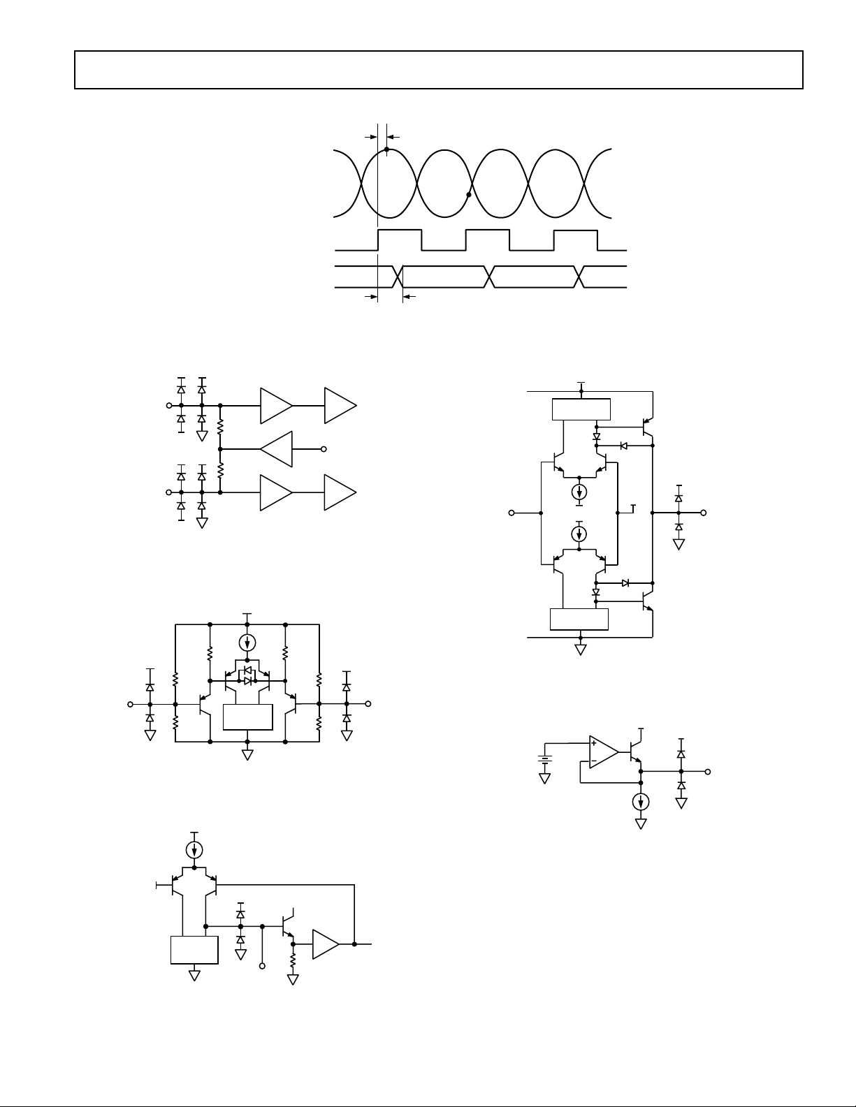
Equivalent Circuits–AD6640
t
A
N
N + 1
ENCODE
DIGITAL OUTPUTS
V
AV
CH
CC
AIN
AIN
V
CL
V
AV
CH
CC
V
CL
BUF
450V
BUF
450V
BUF
Figure 2. Analog Input Stage
AV
CC
AV
CC
R1
17kV
R2
8kV
TIMING
CIRCUITS
(D11–D0)
R1
17kV
R2
8kV
t
OD
Figure 1. Timing Diagram
T/H
V
REF
T/H
AV
CC
ENCODE
DV
CC
CURRENT
MIRROR
CURRENT
MIRROR
N
DV
CC
V
REF
N – 1N – 2
Figure 5. Digital Output Stage
AV
CC
AV
CC
D0–D11
REV. 0
REV. 0
Figure 3. Encode Inputs
AV
CC
V
REF
CURRENT
MIRROR
AV
CC
AV
C1
Figure 4. Compensation Pin, C1
2.4V
0.5mA
V
REF
Figure 6. 2.4 V Reference
CC
–7–
–7–

AD6640
–Typical Performance Characteristics
0
20
40
60
80
100
POWER RELATIVE TO ADC FULL SCALE – dB
120
dc 32.5
4 8 953762
6.5 13.0 19.5 26.0
FREQUENCY – MHz
ENCODE = 65MSPS
AIN = 2.2MHz
Figure 7. Single Tone at 2.2 MHz
0
20
40
60
48 95 37 62
80
ENCODE = 65MSPS
AIN = 15.5MHz
81
80
79
78
WORST CASE HARMONIC – dBc
77
0707
14 21 28 35 42 49 56 63
ANALOG INPUT FREQUENCY – MHz
ENCODE = 65MSPS
TEMP = –40
T = –40 C, +85 C
C, +25 C, & +85 C
T = +25 C
Figure 10. Harmonics vs. AIN
69
68
67
SNR – dB
66
ENCODE = 65MSPS
TEMP = –40
T = +25 C
T = +85 C
C, +25 C, & +85 C
T = –40 C
100
POWER RELATIVE TO ADC FULL SCALE – dB
120
dc 32.5
6.5 13.0 19.5 26.0
FREQUENCY – MHz
Figure 8. Single Tone at 15.5 MHz
0
ENCODE = 65MSPS
AIN = 31.0MHz
20
40
60
80
100
POWER RELATIVE TO ADC FULL SCALE – dB
120
dc 32.5
48 953762
6.5 13.0 19.5 26.0
FREQUENCY – MHz
Figure 9. Single Tone at 31.0 MHz
65
0707
14 21 28 35 42 49 56 63
ANALOG INPUT FREQUENCY – MHz
Figure 11. Noise vs. AIN
90
WORST OTHER SPUR
80
HARMONICS (2nd, 3rd)
70
SNR
60
50
SNR, HARMONICS – dB, dBc
40
30
1 10010
2 4 20 40 200 300
ANALOG INPUT FREQUENCY – MHz
ENCODE = 65MSPS
Figure 12. Harmonics, Noise vs. AIN
–8–
REV. 0
 Loading...