Ultralow Drift,
a
FEATURES
Low Offset Voltage Drift
Matched Offset Voltage
Matched Offset Voltage Over Temperature
Matched Bias Currents
Crosstalk: –124 dB at 1 kHz
Low Bias Current: 35 pA max Warmed Up
Low Offset Voltage: 250 mV max
Low Input Voltage Noise: 2 mV p-p
High Open Loop Gain: 108 dB
Low Quiescent Current: 2.8 mA max
Low Total Harmonic Distortion
Standard Dual Amplifier Pinout
Available in Hermetic Metal Can Package, Hermetic
Surface Mount (20-Pin LCC) and Chip Form
MIL-STD-883B Processing Also Available
Single Version Available: AD547
Dual BiFET Op Amp
AD647
PRODUCT DESCRIPTION
The AD647 is an ultralow drift, dual JFET amplifier that combines high performance and convenience in a single package.
The AD647 uses the most advanced ion-implantation and laser
wafer drift trimming technologies to achieve the highest performance currently available in a dual JFET. Ion-implantation permits the fabrication of matched JFETs on a monolithic bipolar
chip. Laser wafer drift trimming trims both the initial offset voltage and its drift with temperature to provide offsets as low as
100 µV (250 µV max) and drifts of 2.5 µV/°C max.
In addition to outstanding individual amplifier performance, the
AD647 offers guaranteed and tested matching performance on
critical parameters such as offset voltage, offset voltage drift and
bias currents.
The high level of performance makes the AD647 especially well
suited for high precision instrumentation amplifier applications
that previously would have required the costly selection and
matching of space wasting single amplifiers.
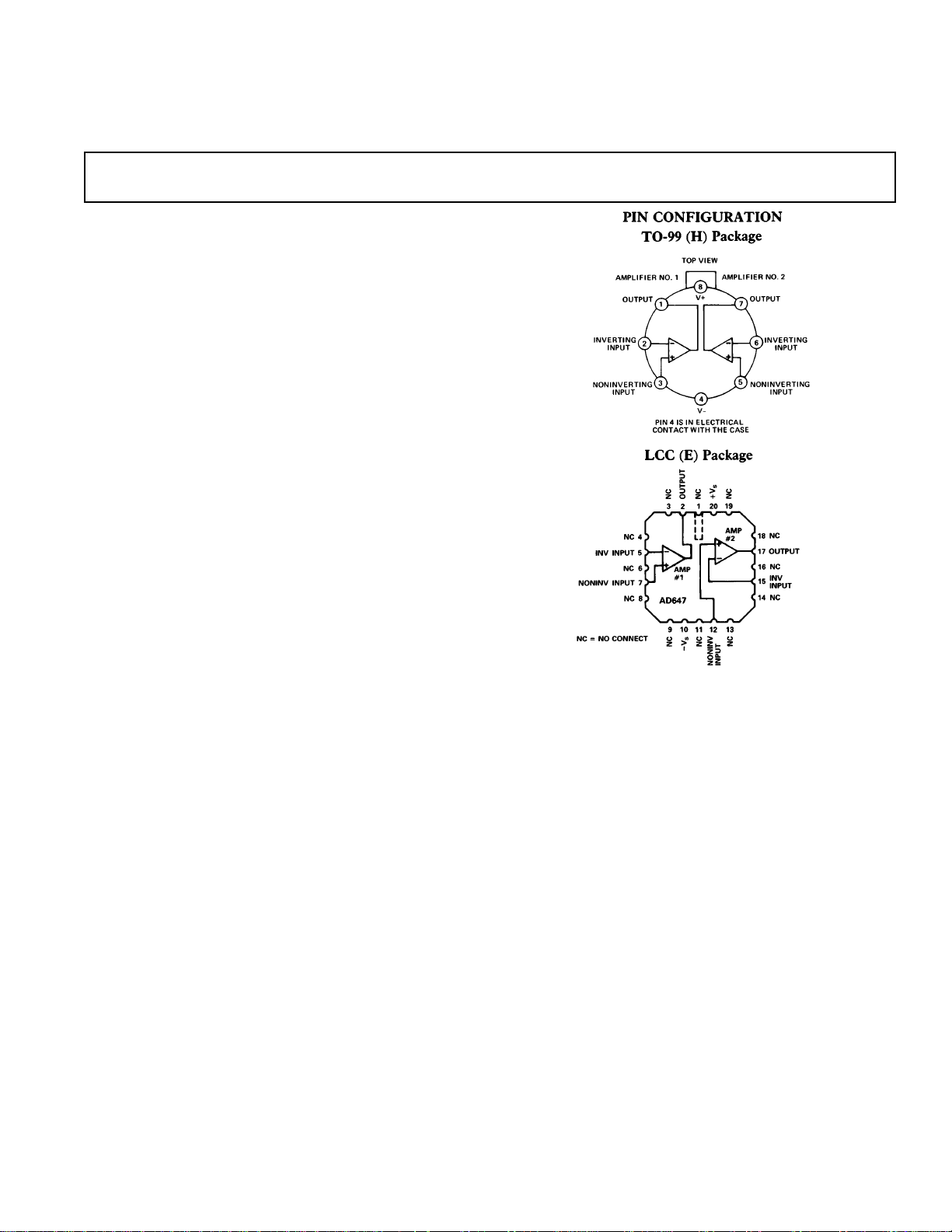
The AD647 is offered in four performance grades, three commercial (the J, K and L) and one extended (the S). All are supplied in hermetically sealed 8-pin TO-99 packages and are
available processed to MIL-STD-883B. The LCC version is
also available processed to MIL-STD-883B.
REV. A
Information furnished by Analog Devices is believed to be accurate and
reliable. However, no responsibility is assumed by Analog Devices for its
use, nor for any infringements of patents or other rights of third parties
which may result from its use. No license is granted by implication or
otherwise under any patent or patent rights of Analog Devices.
PRODUCT HIGHLIGHTS
1. The AD647 is guaranteed and tested to tight matching specifications to ensure high performance and to eliminate the selection and matching of single devices.
2. Laser wafer drift trimming reduces offset voltage and offset
voltage drifts to 250 µV and 2.5 µV/°C max.
3. Voltage noise is guaranteed at 4 µV p-p max (0.1 Hz to
10 Hz) on K, L and S grades.
4. Bias current (35 pA K, L, S; 75 pA J) is specified after five
minutes of operation.
5. Total supply current is a low 2.8 mA max.
6. High open loop gain ensures high linearity in precision instrumentation amplifier applications.
7. The standard dual amplifier pinout permits the direct substitution of the AD647 for lower performance devices.
8. The AD647 is available in chip form.
One Technology Way, P.O. Box 9106, Norwood, MA 02062-9106, U.S.A.
Tel: 617/329-4700 Fax: 617/326-8703

AD647–SPECIFICATIONS
(@ +258C and VS = 615 V dc)
Model AD647J AD647K AD647L AD647S
Min Typ Max Min Typ Max Min Typ Max Min Typ Max Units
OPEN LOOP GAIN
VO = ± 10 V, RL ≥ 2 kΩ 100,000 250,000 250,000 250,000 V/V
T
to T
MIN
, RL = 2 kΩ 100,000 250,000 250,000 100,000 V/V
MAX
OUTPUT CHARACTERISTICS
Voltage @ R
Voltage @ R
Short Circuit Current 25 25 25 25 mA
= 2 kΩ, T
L
= 10 kΩ, T
L
MIN
MIN
to T
to T
610 ±12 610 ±12 610 ±12 610 ±12 V
MAX
612 ±13 612 ±13 612 ±13 612 ±13 V
MAX
FREQUENCY RESPONSE
Unity Gain Small Signal 1.0 1.0 1.0 1.0 MHz
Full Power Response 50 50 50 50 kHz
Slew Rate, Unity Gain 2.0 3.0 2.0 3.0 2.0 3.0 2.0 3.0 V/µs
INPUT OFFSET VOLTAGE
1
Initial Offset 1.0 0.5 0.25 0.5 mV
Input Offset Voltage vs. Temperature 10 5 2.5 5.0 µV/°C
Input Offset Voltage vs. Supply,
T
to T
MIN
MAX
INPUT BIAS CURRENT
2
200 100 100 100 µV/V
Either Input 10 75 10 35 10 35 10 35 pA
Offset Current 5222pA
MATCHING CHARACTERISTICS
3
Input Offset Voltage 1.0 0.5 0.25 0.5 mV
Input Offset Voltage T
Input Bias Current 35 25 25 25 pA
MIN
to T
MAX
10 5 2.5 10.0 µV/°C
Crosstalk –124 –124 –124 –124 dB
INPUT IMPEDANCE
Differential 10
Common Mode 1012i610
INPUT VOLTAGE RANGE
Differential
4
12
i610
12
i610
12
i610
12
i610
12
i610
12
i6MΩipF
12
i6MΩipF
±20 ±20 ±20 ±20 V
Common Mode 610 ±12 610 ±12 610 ±12 610 ±12 V
Common-Mode Rejection 76 80 80 80 dB
INPUT NOISE
Voltage 0.1 Hz to 10 Hz 2 444µV p-p
f = 10 Hz 70 70 70 70 nV/√Hz
f = 100 Hz 45 45 45 45 nV/√Hz
f = 1 kHz 30 30 30 30 nV/√
Hz
f = 10 kHz 25 25 25 25 nV/√Hz
POWER SUPPLY
Rated Performance ± 15 ±15 ± 15 ±15 V
Operating ± 5 ±18 ±5 ±18 ±5 ± 18 ± 5 ±18 V
Quiescent Current 2.8 2.8 2.8 2.8 mA
TEMPERATURE RANGE
Operating, Rated Performance 0 +70 0 +70 0 +70 –55 +125 °C
Storage –65 +150 –65 +150 –65 +150 –65 +150 °C
PACKAGE OPTION
TO-99 Style (H-08B) AD647JH AD647KH AD647LH AD647SH
LCC (E-20A) AD647SE
AD647SE/883BH
NOTES
1
Input Offset Voltage specifications are guaranteed after 5 minutes of operation at TA = +25°C.
2
Bias Current specifications are guaranteed at maximum at either input after 5 minutes of operation at TA = +25°C. For higher temperatures, the current doubles every 10°C.
3
Matching is defined as the difference between parameters of the two amplifiers.
4
Defined as the maximum safe voltage between inputs, such that neither exceeds ±10 V from ground.
Specifications shown in boldface are tested on all production units at final electrical test. Results from those tests are used to calculate outgoing quality levels. All min and max specifications
are guaranteed, although only those shown in boldface are tested on all production units.
Specifications subject to change without notice.
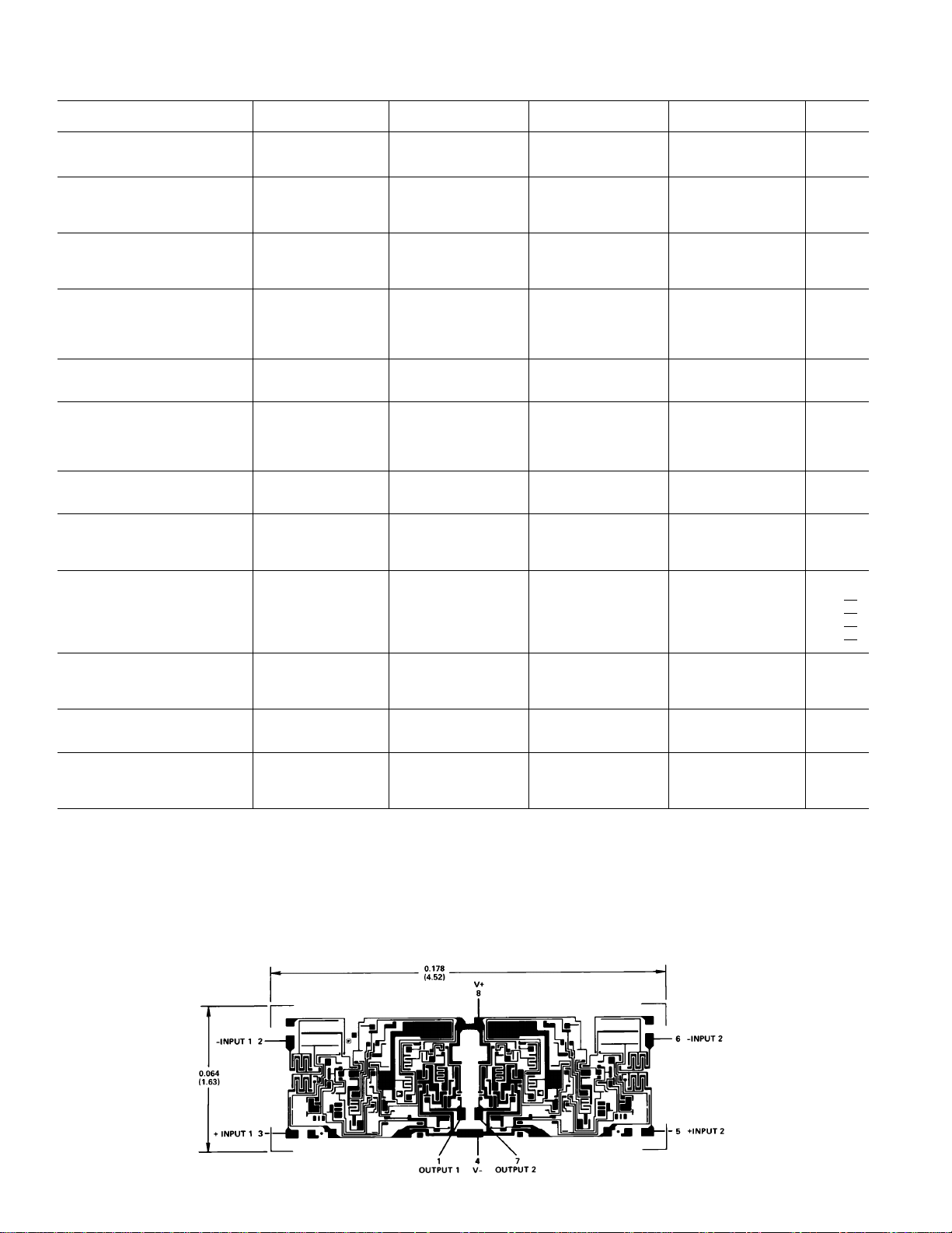
METALIZATION PHOTOGRAPH
Dimensions shown in inches and (mm).
Contact factory for latest dimensions.
–2–
REV. A
 Loading...