Analog Devices AD5263 Datasheet

Quad, 15 V, 256-Position, Digital
Potentiometer with Pin Selectable SPI/I
FEATURES
256-position, 4-channel
End-to-end resistance 20 kΩ, 50 kΩ, 200 kΩ
Pin selectable SPI® or I
Power-on preset to midscale
Two package address decode pins AD0 and AD1
Rheostat mode temperature coefficient 30 ppm/°C
Voltage divider temperature coefficient 5 ppm/°C
Wide operating temperature range –40°C to +125°C
5 V to 15 V single supply; ±5 V dual supply
APPLICATIONS
Mechanical potentiometer replacement
Optical network adjustment
Instrumentation: gain, offset adjustment
Stereo channel audio level control
Automotive electronics adjustment
Programmable power supply
Programmable filters, delays, time constants
Line impedance matching
Low resolution DAC/trimmer replacement
Base station power amp biasing
Sensor calibration
GENERAL DESCRIPTION
The AD5263 is the industry’s first quad-channel, 256-position,
digital potentiometer
device performs the same electronic adjustment function as
mechanical potentiometers or variable resistors, with enhanced
resolution, solid-state reliability, and superior low temperature
coefficient performance.
Each channel of the AD5263 offers a completely programmable
value of resistance between the A terminal and the wiper, or
between the B terminal and the wiper. The fixed A-to-B
terminal resistance of 20 kΩ, 50 kΩ, or 200 kΩ has a nominal
temperature coefficient of ±30 ppm/°C and a ±1% channel-to-
2
C® compatible interface
1
with a selectable digital interface. This
2
AD5263
channel matching tolerance. Another key feature of this part is
the ability to operate from +4.5 V to +15 V, or at ±5 V.
Wiper position programming presets to midscale upon poweron. Once powered, the VR wiper position is programmed by
either the 3-wire SPI or 2-wire I
2
I
C mode, additional programmable logic outputs enable users
to drive digital loads, logic gates, and analog switches in their
systems.
The AD5263 is available in a narrow body TSSOP-24. All parts
are guaranteed to operate over the automotive temperature
range of –40°C to +125°C.
For single- or dual-channel applications, refer to the
AD5260/AD5280 or AD5262/AD5282.
FUNCTIONAL BLOCK DIAGRAM
A1
V
DD
V
SS
SHDN
RES/AD1
V
L
CLK/SCL
SDI/SDA
CS/AD0
GND
1
The terms digital potentiometer, VR, and RDAC are used interchangeably.
Purchase of licensed I2C components of Analog Devices or one of its sublicensed
Associated Companies conveys a license for the purchaser under the Philips I
Patent Rights to use these components in an I
conforms to the I
W1 B1 A2
RDAC 1
REGISTER
2
C Standard Specification as defined by Philips.
REGISTER
ADDRESS
DECODER
2
SPI/I
C
SELECT
LOGIC
DIS
2
C compatible interface. In the
W2 B2
RDAC 2
SERIAL INPUT
Figure 1.
REGISTER
A3
RDAC 3
REGISTER
8
NC/O2
W3
B3 A4
SDO/O1
2
C system, provided that the system
W4 B4
RDAC 4
REGISTER
AD5263
2
C
C
03142-0-001
Rev. 0
Information furnished by Analog Devices is believed to be accurate and reliable.
However, no responsibility is assumed by Analog Devices for its use, nor for any
infringements of patents or other rights of third parties that may result from its use.
Specifications subject to change without notice. No license is granted by implication
or otherwise under any patent or patent rights of Analog Devices. Trademarks and
registered trademarks are the property of their respective companies.
One Technology Way, P.O. Box 9106, Norwood, MA 02062-9106, U.S.A.
Tel: 781.329.4700 www.analog.com
Fax: 781.326.8703 © 2003 Analog Devices, Inc. All rights reserved.

AD5263
TABLE OF CONTENTS
Electrical Characteristics—20 kΩ, 50 kΩ, 200 kΩ Versions ....... 3
Applications..................................................................................... 20
Timing Characteristics—20 kΩ, 50 kΩ, 200 kΩ Versions........... 4
Absolute Maximum Ratings............................................................ 5
Typical Performance Characteristics ............................................. 6
Test Circuits..................................................................................... 11
SPI Compatible Digital Interface (DIS = 0)................................ 12
I2C Compatible Digital Interface (DIS = 1).................................13
Operation......................................................................................... 14
Programming the Variable Resistor .........................................14
Programming the Potentiometer Divider ............................... 15
Pin Selectable Digital Interface................................................. 15
SPI Compatible 3-Wire Serial Bus (DIS = 0).......................... 15
I2C Compatible 2-Wire Serial Bus (DIS = 1) .......................... 16
Additional Programmable Logic Output ................................17
Self-Contained Shutdown Function ........................................ 17
Multiple Devices on One Bus ...................................................17
Level Shift for Negative Voltage Operation............................. 17
ESD Protection ........................................................................... 18
Terminal Voltage Operating Range.......................................... 18
Power-Up Sequence ................................................................... 18
V
Power Supply ................................................................... 18
LOGIC
Layout and Power Supply Bypassing ....................................... 18
Bipolar DC or AC Operation from Dual Supplies................. 20
Gain Control Compensation.................................................... 20
Programmable Voltage Reference ............................................ 20
8-Bit Bipolar DAC ...................................................................... 21
Bipolar Programmable Gain Amplifier................................... 21
Programmable Voltage Source with Boosted Output............ 21
Programmable 4–20 mA Current Source ............................... 22
Programmable Bidirectional Current Source......................... 22
Programmable Low-Pass Filter ................................................ 23
Programmable Oscillator.......................................................... 23
Resistance Scaling ...................................................................... 24
Resistance Tolerance, Drift, and Temperature Coefficient
Mismatch Considerations
Pin Configuration and Pin Function Descriptions.................... 25
Pin Configuration ...................................................................... 25
Pin Function Descriptions........................................................ 25
Outline Dimensions....................................................................... 26
ESD Caution................................................................................ 26
Ordering Guide............................................................................... 26
......................................................... 24
RDAC Circuit Simulation Model ............................................. 19
REVISION HISTORY
Revision 0: Initial Version
Rev. 0 | Page 2 of 28
AD5263
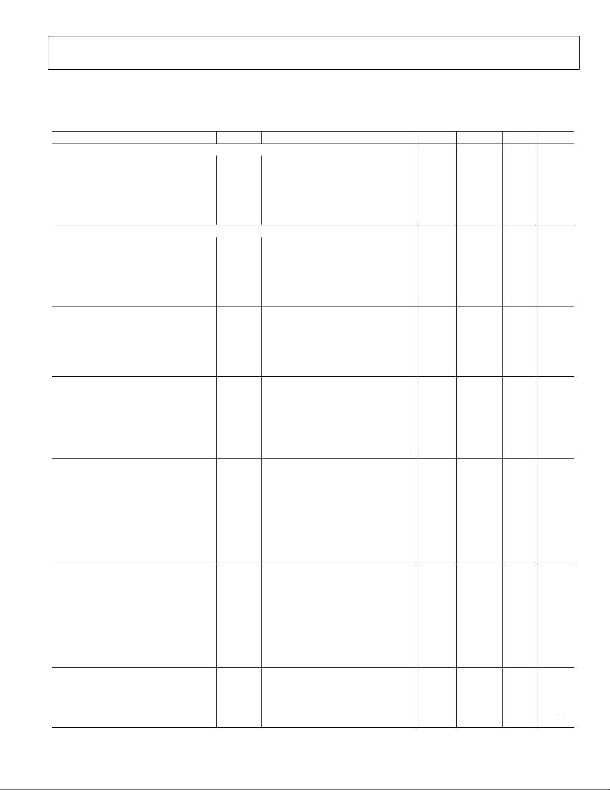
ELECTRICAL CHARACTERISTICS—20 kΩ, 50 kΩ, 200 kΩ VERSIONS
(VDD = +5 V, VSS = –5 V, VL = +5 V, VA = +VDD, VB = 0 V, –40°C < TA < +125°C, unless otherwise noted.)
Table 1.
Parameter Symbol Conditions Min Typ1 Max Unit
DC CHARACTERISTICS—RHEOSTAT MODE (Specifications apply to all VRs.)
Resistor Differential NL2 R-DNL RWB, VA=NC –1 ±1/4 +1 LSB
Resistor Nonlinearity2 R-INL RWB, VA=NC –1 ±1/2 +1 LSB
Nominal Resistor Tolerance3 ∆RAB T
∆RWB/∆T 30 ppm/°C Resistance Mode Temperature
Coefficient
∆RWA/∆T 30 ppm/°C
Wiper Resistance RW I
DC CHARACTERISTICS—POTENTIOMETER DIVIDER MODE (Specifications apply to all VRs.)
Resolution N 8 Bits
Differential Nonlinearity4 DNL –1 ±1/4 +1 LSB
Integral Nonlinearity4 INL –1 ±1/2 +1 LSB
Voltage Divider Temperature Coefficient ∆VW/∆T Code = 0x80 5 ppm/°C
Full-Scale Error V
Zero-Scale Error V
Code = 0xFF –2 –1 +0 LSB
WFSE
Code = 0x00 0 +1 +2 LSB
WZSE
RESISTOR TERMINALS
Voltage Range5 V
Capacitance6 Ax, Bx C
V
A,B,W
f = 1 MHz, measured to GND, Code = 0x80 25 pF
A,B
Capacitance6 Wx CW f = 1 MHz, measured to GND, Code = 0x80 55 pF
Common-Mode Leakage ICM V
Shutdown Current
7
I
0.02 5 µA
SHDN
DIGITAL INPUTS
Input Logic High VIH 2.4 V
Input Logic Low VIL 0.8 V
Input Logic High (SDA and SCL) VIH V
Input Logic Low (SDA and SCL) VIL V
Input Current IIL V
Input Capacitance6 C
5 pF
IL
DIGITAL OUTPUTS
SDA VOL I
VOL I
O1, O2 VOH I
O1, O2 VOL I
SDO VOH R
SDO VOL I
Three-State Leakage Current IOZ V
Output Capacitance6 C
3 8 pF
OZ
POWER SUPPLIES
Logic Supply
Power Single-Supply Range V
Power Dual-Supply Range V
Logic Supply Current
8
9
VL 2.7 5.5 V
DD RANGE
DD/SS RANGE
I
L
Positive Supply Current IDD V
Negative Supply Current ISS V
Power Dissipation10 P
V
DISS
Power Supply Sensitivity PSS ∆VDD = +5 V ± 10% 0.002 0.01 %/%
DYNAMIC CHARACTERISTICS
6, 11
Bandwidth (3 dB) BW RAB = 20 kΩ/50 kΩ/200 kΩ 300/150/35 kHz
Total Harmonic Distortion THDW V
VW Settling Time
Resistor Noise Voltage e
12
tS V
RWB = 10 kΩ, f = 1 kHz, RS = 0 9
N_WB
= 25°C –30 30 %
A
= 1 V/RAB 60 150 Ω
W
V
SS
= VB = VDD/2 1 nA
A
= 0 V 0.7 × VL VL + 0.5 V
SS
= 0 V –0.5 0.3 × VL V
SS
= 0 V or +5 V ±1 µA
IN
= 3 mA 0.4 V
SINK
= 6 mA 0.6 V
SINK
= 40 µA 4 V
SOURCE
= 1.6 mA 0.4 V
SINK
= 2.2 kΩ to VDD V
L
= 3 mA 0.4 V
SINK
= 0 V or +5 V ±1 µA
IN
– 0.1 V
DD
V
DD
VSS = 0 V VL 16.5 V
±4.5 ±7.5 V
V
= +5 V 25 60 µA
L
= +5 V or VIL = 0 V 1 µA
IH
= –5 V 1 µA
SS
= +5 V or VIL = 0 V, VDD = +5 V, VSS = –5 V 0.6 mW
IH
= 1 V rms, VB = 0 V, f = 1 kHz, RAB = 20 kΩ 0.05 %
A
= 10 V, VB = 0 V, ±1 LSB error band 2 µs
A
Hz
nV/√
Rev. 0 | Page 3 of 28
AD5263
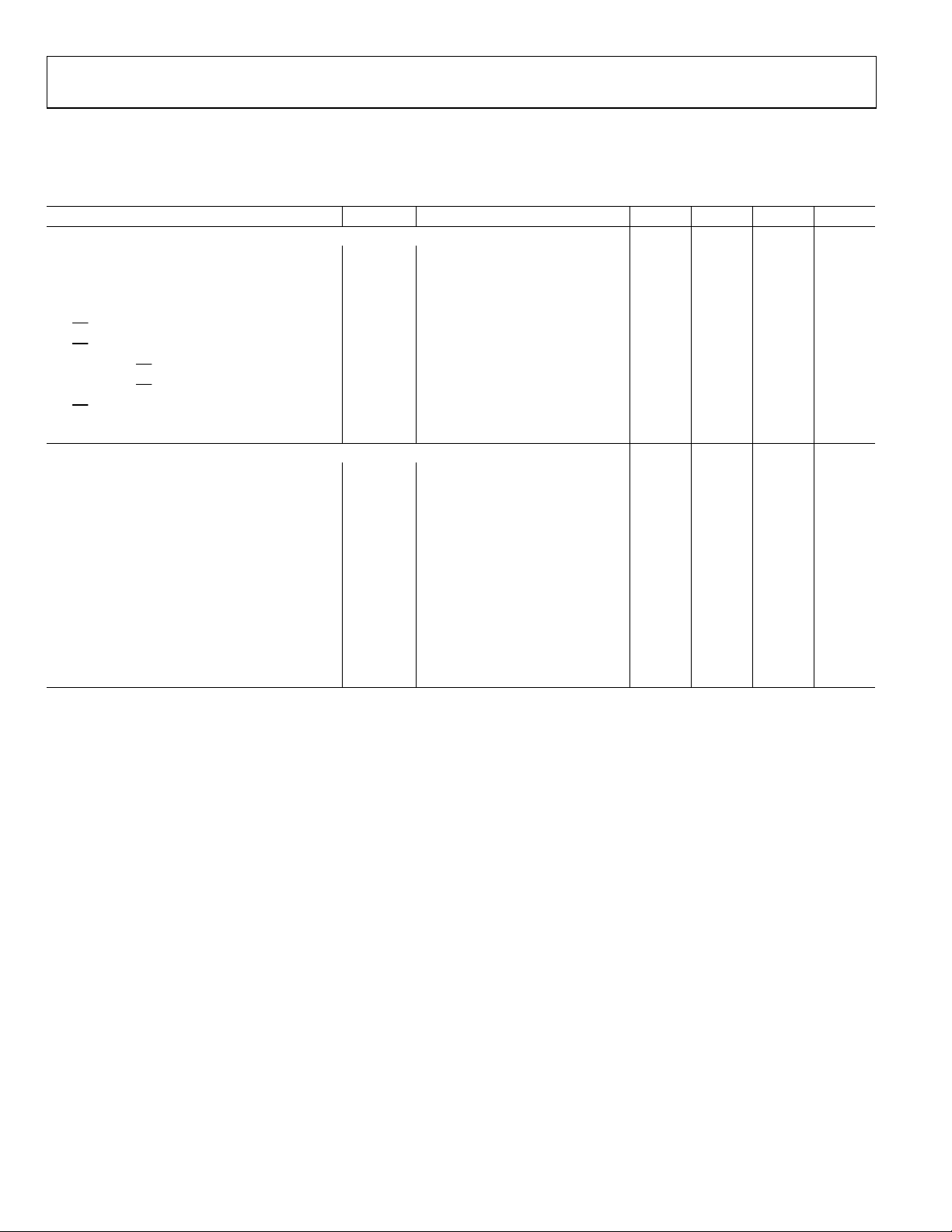
TIMING CHARACTERISTICS—20 kΩ, 50 kΩ, 200 kΩ VERSIONS
(V
= +5 V, V
DD
Table 2.
Parameter Symbol Conditions Min Typ1 Max Unit
SPI INTERFACE TIMING CHARACTERISTICS (Specifications Apply to All Parts
Clock Frequency f
Input Clock Pulsewidth tCH,tCL Clock level high or low 20 ns
Data Setup Time tDS 10 ns
Data Hold Time tDH 10 ns
CS Setup Time
CS High Pulsewidth
CLK Fall to CS Fall Hold Time
CLK Fall to CS Rise Hold Time
CS Rise to Clock Rise Setup
Reset Pulsewidth t
I2C INTERFACE TIMING CHARACTERISTICS (Specifications Apply to All Parts
SCL Clock Frequency f
t
Bus Free Time between STOP and START t1 1.3 µs
BUF
t
t
t
t
t
t
Hold Time (Repeated START) t2
HD;STA
Low Period of SCL Clock t3 1.3 µs
LOW
High Period of SCL Clock t4 0.6 50 µs
HIGH
Setup Time for START Condition t5 0.6 µs
SU;STA
HD;DAT
Data Setup Time t7 100 ns
SU;DAT
tF Fall Time of both SDA and SCL Signals t8 300 ns
tR Rise Time of Both SDA and SCL Signals t9 300 ns
t
NOTES
1
2
3
4
5
6
7
8
9
10
11
12
13
Setup Time for STOP Condition t10 0.6 µs
SU;STO
Typicals represent average readings at 25°C and VDD = +5 V, VSS = –5 V.
Resistor position nonlinearity error (R-INL) is the deviation from an ideal value measured between the maximum resistance and the minimum resistance wiper
positions. R-DNL measures the relative step change from ideal between successive tap positions. Parts are guaranteed monotonic. IW = VDD/R for both VDD = +5 V and
VSS = –5 V.
VAB = VDD, Wiper (VW) = no connect.
INL and DNL are measured at VW with the RDAC configured as a potentiometer divider similar to a voltage output D/A converter. VA = VDD and VB = 0 V.
DNL specification limits of ±1 LSB maximum are guaranteed monotonic operating conditions.
Resistor Terminals A, B, and W have no limitations on polarity with respect to each other.
Guaranteed by design and not subject to production test.
Measured at the Ax terminals. All Ax terminals are open circuited in shutdown mode.
VL is limited to VDD or 5.5 V, whichever is less.
Worst-case supply current consumed when all logic-input levels set at 2.4 V, standard characteristic of CMOS logic.
P
is calculated from (IDD × VDD). CMOS logic level inputs result in minimum power dissipation.
DISS
All dynamic characteristics use VDD = +5 V, VSS = –5 V, VL = +5 V.
Settling time depends on value of VDD, RL, and CL.
See timing diagrams for location of measured values. All input control voltages are specified with tR = tF = 2 ns (10% to 90% of +3 V) and timed from a voltage level
of 1.5 V. Switching characteristics are measured using V
= –5 V, VL = +5 V, VA = +VDD, VB = 0 V, –40°C < TA < +125°C unless otherwise noted.)
SS
6, 13
)
25 MHz
CLK
15 ns
t
CSS
t
20 ns
CSW
t
0 ns
CSH0
t
0 ns
CSH1
10 ns
t
CS1
RS
400 kHz
SCL
6, 13
)
After this period, the first clock
5 ns
0.6 µs
pulse is generated.
Data Hold Time t6 0.9 µs
= +5 V.
L
Rev. 0 | Page 4 of 28
AD5263
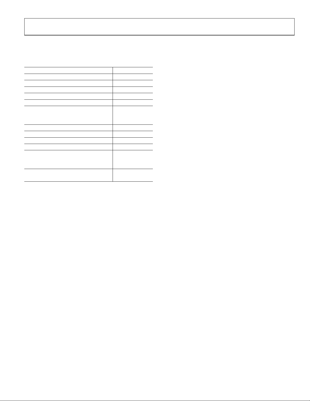
ABSOLUTE MAXIMUM RATINGS
(TA = +25°C, unless otherwise noted.)
Table 3.
Parameter Value
VDD to GND –0.3 V to +16.5 V
VSS to GND 0 V to +7.5 V
VDD to VSS +16.5 V
VL to GND –0.3 V to +6.5 V
VA, VB, VW to GND VSS to V
DD
Terminal Current, Ax-Bx, Ax-Wx, Bx-Wx
Pulsed1 ±20 mA
Continuous ±3 mA
Stresses above those listed under Absolute Maximum Ratings
may cause permanent damage to the device. This is a stress
rating only; functional operation of the device at these or any
other conditions above those indicated in the operational
section of this specification is not implied. Exposure to absolute
maximum rating conditions for extended periods may affect
device reliability.
Digital Inputs and Output Voltage to GND 0 V to +7 V
Operating Temperature Range –40°C to +85°C
Maximum Junction Temperature (T
) 150°C
J MAX
Storage Temperature –65°C to +150°C
Lead Temperature (Soldering, 10 sec) 300°C
Vapor Phase (60 sec) 215°C
Infrared (15 sec) 220°C
Thermal Resistance2 θJA
TSSOP-24 143°C/W
1
Maximum terminal current is bounded by the maximum current handling of
the switches, maximum power dissipation of the package, and maximum
applied voltage across any two of the A, B, and W terminals at a given
resistance.
2
Package power dissipation: (T
JMAX
– TA)/θJA.
Rev. 0 | Page 5 of 28
AD5263
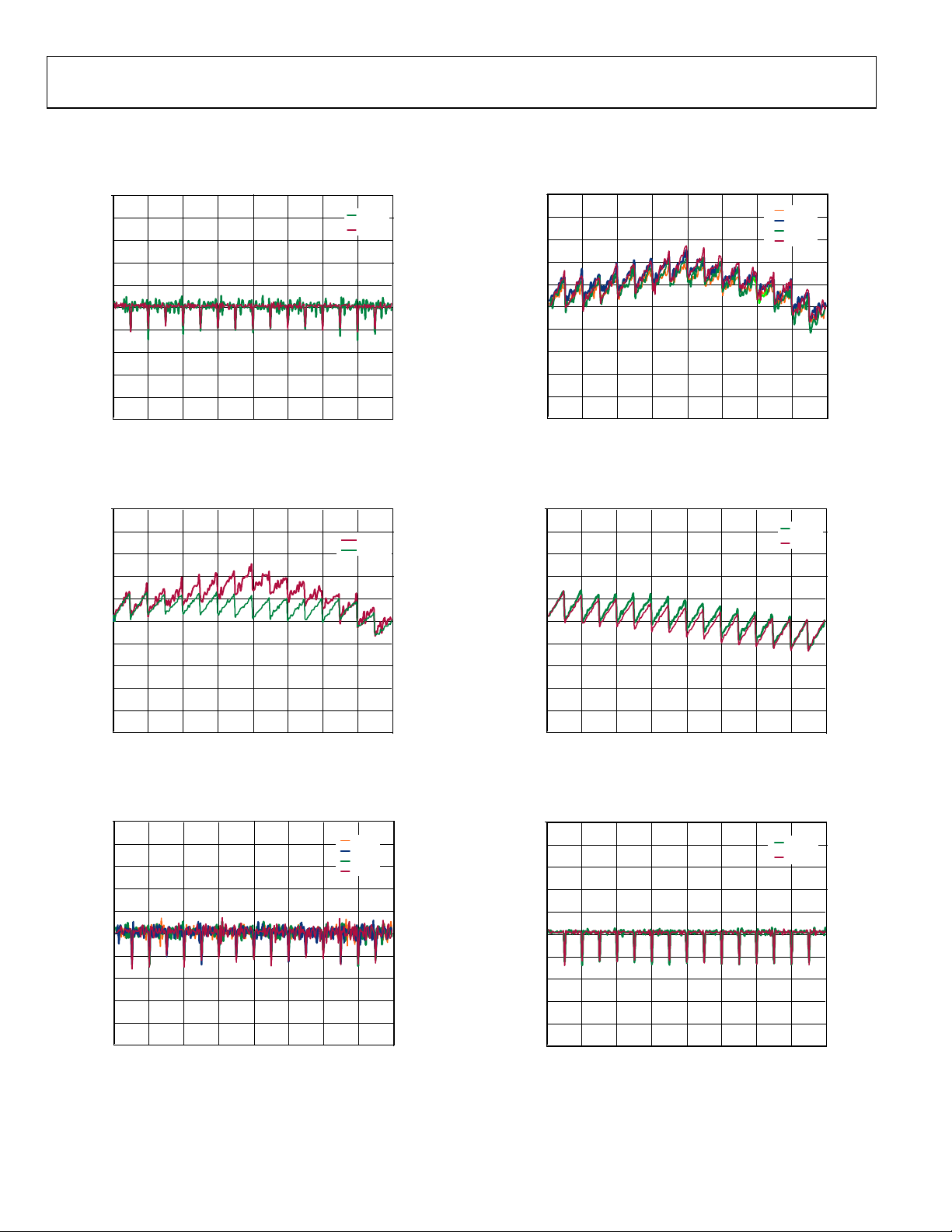
TYPICAL PERFORMANCE CHARACTERISTICS
(RAB = 20 kΩ unless otherwise noted.)
1
±5V
15/0V
03142-0-073
RHEOSTAT MODE DNL (LSB)
0.6
0.4
0.2
–0.2
–0.4
–0.6
–0.8
0.8
0
–1
32
64 96 1280
CODE (Decimal)
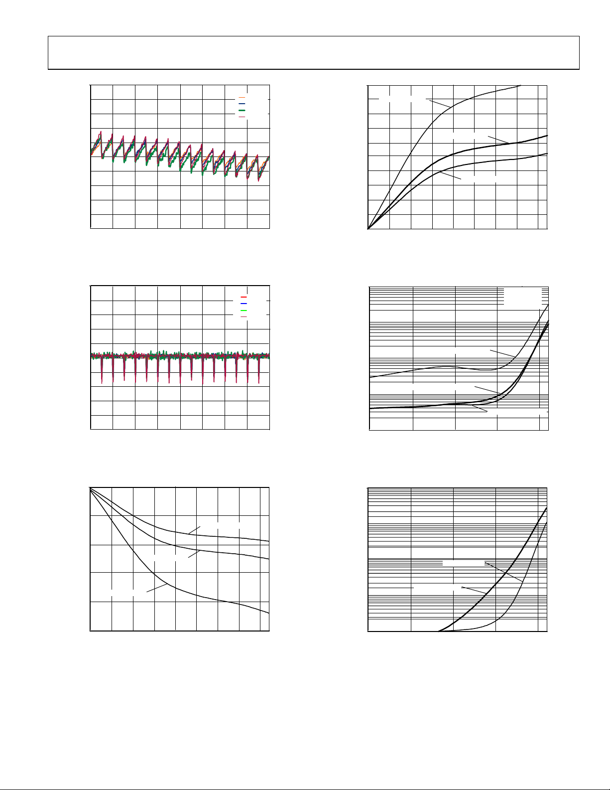
Figure 2. R-DNL vs. Code vs. Supply Voltage
160 192 224 256
1
0.8
0.6
0.4
0.2
0
–0.2
–0.4
RHEOSTAT MODE INL (LSB)
–0.6
–0.8
–1
32
64 96 1280
Figure 5. R-INL vs. Code; V
CODE (Decimal)
–40°C
25°C
85°C
125°C
160 192 224 256
= ±5 V
DD
03142-0-004
1
0.8
0.6
0.4
0.2
0
–0.2
–0.4
RHEOSTAT MODE INL (LSB)
–0.6
–0.8
–1
32
64 96 1280
Figure 3. R-INL vs. Code vs. Supply Voltage
1
0.8
0.6
0.4
0.2
0
–0.2
–0.4
RHEOSTAT MODE DNL (LSB)
–0.6
–0.8
–1
32
64 96 1280
Figure 4. R-DNL vs. Code; V
CODE (Decimal)
CODE (Decimal)
±5V
15/0V
160 192 224 256
–40°C
25°C
85°C
125°C
160 192 224 256
= ±5 V
DD
03142-0-002
03142-0-003
1
0.8
0.6
0.4
0.2
0
–0.2
–0.4
–0.6
POTENTIOMETER MODE INL (LSB)
–0.8
–1
32
64 96 1280
CODE (Decimal)
160 192 224 256
±5V
15/0V
03142-0-005
Figure 6. INL vs. Code vs. Supply Voltage
1
0.8
0.6
0.4
0.2
0
–0.2
–0.4
–0.6
POTENTIOMETER MODE DNL (LSB)
–0.8
–1
32
64 96 1280
CODE (Decimal)
160 192 224 256
±5V
15/0V
03142-0-006
Figure 7. DNL vs. Code vs. Supply Voltage
Rev. 0 | Page 6 of 28
AD5263
POTENTIOMETER MODE INL (LSB)
0.8
0.6
0.4
0.2
–0.2
–0.4
–0.6
–0.8
1
–40°C
25°C
85°C
125°C
0
–1
32
64 96 1280
CODE (Decimal)
Figure 8. INL vs. Code; V
160 192 224 256
= ±5 V
DD
03142-0-007
2
VDD/VSS = 4.5/0V
1.8
1.6
1.4
1.2
1
0.8
ZSE (LSB)
0.6
0.4
0.2
0
–20
0
VDD/VSS = ±5V
VDD/VSS = 16.5/0V
40 100
20 60 80–40
TEMPERATURE (°C)
03142-0-010
120
Figure 11. Zero-Scale Error vs. Temperature
1
0.8
0.6
0.4
0.2
0
–0.2
–0.4
–0.6
POTENTIOMETER MODE DNL (LSB)
–0.8
–1
0
–0.5
–1
–1.5
FSE (LSB)
–2
32
64 96 1280
Figure 9. DNL vs. Code; V
VDD/VSS = 4.5/0V
CODE (Decimal)
VDD/VSS = ±5V
–40°C
25°C
85°C
125°C
160 192 224 256
= ±5 V
DD
VDD/VSS = 16.5/0V
03142-0-008
SUPPLY CURRENT (µA)
SS
/I
DD
I
0.001
SHUTDOWN CURRENT (µA)
0.01
0.1
0.01
10
1
0.1
ISS@ VDD/VSS = ±5V
IDD @ VDD/VSS = 15/0V
0
40
TEMPERATURE (°C)
TEMPERATURE (°C)
Figure 12. Supply Current vs. Temperature
10
1
VDD/VSS = ±5V
VDD/VSS = 15/0V
V
= 5V
LOGIC
= 5V
V
IH
= 0V
V
IL
IDD@VDD/VSS = ±5V
80–40
120
03142-0-011
–2.5
20 60 80–40
–20
0
40 100
TEMPERATURE (°C)
Figure 10. Full-Scale Error vs. Temperature
03142-0-009
120
Rev. 0 | Page 7 of 28
0.001
0
40
TEMPERATURE (°C)
80–40
Figure 13. Shutdown Current vs. Temperature
03142-0-012
120
AD5263
27
26
25
(µA)
LOGIC
24
I
VDD/VSS = 15/0V
VDD/VSS = ±5V
150
100
–50
–100
20k
Ω
50k
Ω
200k
50
0
Ω
23
22
0
Figure 14. I
85
80
75
70
65
60
WIPER RESISTANCE (Ω)
55
50
45
0
40
TEMPERATURE (°C)
vs. Temperature
LOGIC
RON @ VDD/VSS = 15/0V
510–5 15
V
(V)
BIAS
Figure 15. Wiper ON Resistance vs. Bias Voltage
80–40
RON @ VDD/VSS = 5/0V
RON @ VDD/VSS = ±5V
120
03142-0-013
03142-0-014
–150
–200
POTENTIOMETER MODE TEMPCO (ppm/°C)
–250
32
64 96 1280
CODE (Decimal)
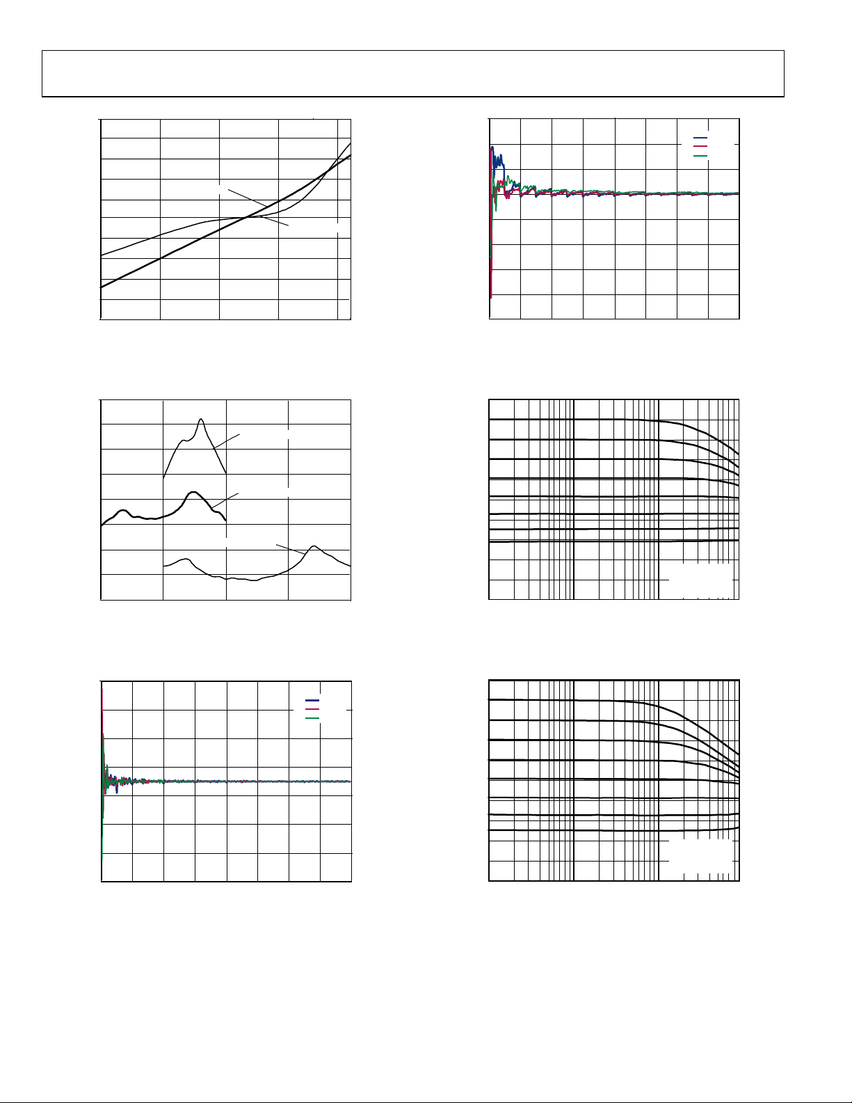
Figure 17. Potentiometer Mode Tempco ∆R
0
–6
–12
–18
–24
–30
–36
GAIN (dB)
–42
–48
–54
–60
1k
0x80
0x40
0x20
0x10
0x08
0x04
0x02
0x01
FREQUENCY (Hz)
Figure 18. Gain vs. Frequency vs. Code; R
160 192 224 256
/∆T vs. Code
WB
= 25°C
T
A
= 50mV rms
V
A
=±5V
V
DD/VSS
100k10k
= 20 kΩ
AB
1M
03142-0-016
03142-0-017
700
500
300
100
–100
–300
RHEOSTAT MODE TEMPCO (ppm/°C)
–500
–700
32
64 96 1280
CODE (Decimal)
Figure 16. Rheostat Mode Tempco ∆R
20kΩ
50kΩ
200kΩ
160 192 224 256
/∆T vs. Code
WB
03142-0-015
Rev. 0 | Page 8 of 28
0
–6
–12
–18
–24
–30
–36
GAIN (dB)
–42
–48
–54
–60
1k
0x80
0x40
0x20
0x10
0x08
0x04
0x02
0x01
FREQUENCY (Hz)
Figure 19. Gain vs. Frequency vs. Code; R
TA = 25°C
=50mVrms
V
A
=±5V
V
DD/VSS
100k10k
03142-0-018
1M
= 50 kΩ
AB
AD5263
0
–6
–12
–18
–24
–30
–36
GAIN (dB)
–42
–48
–54
–60
1k
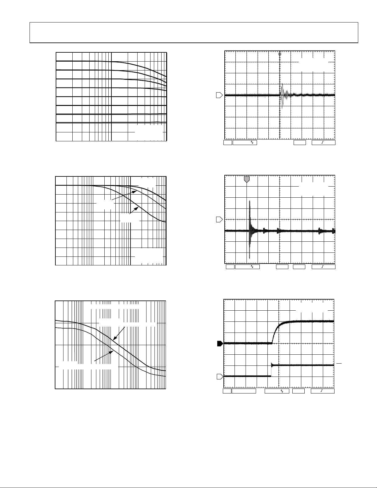
Figure 20. Gain vs. Frequency vs. Code; R
0x80
0x40
0x20
0x10
0x08
0x04
0x02
0x01
FREQUENCY (Hz)
TA = 25°C
= 50mV rms
V
A
V
DD/VSS
= 200 kΩ
AB
=±5V
Code = 0x80
VDD/VSS = ±5.5V
=±5V
V
B/VA
V
1
03142-0-019
100k10k
Ch 1 50.0mV M 100ns A CH2 2.70 V
Figure 23. Digital Feedthrough
W
03142-0-022
GAIN (dB)
PSRR (–dB)
–12
–18
–24
–30
–36
–42
–48
–54
–60
–6
80
60
40
20
0
0
1k
100
Figure 21. –3 db Bandwidth
+PSRR @
V
= ±5V DC ± 10% p-p AC
DD/VSS
Figure 22. PSRR v s. Frequency
R = 50kΩ
150kHz
R = 200kΩ
35kHz
TA = 25°C
V
V
FREQUENCY (Hz)
CODE = 0x80, VA = VDD, VB = 0V
–PSRR @
V
DD/VSS
FREQUENCY (Hz)
100k10k
= ±5V DC ± 10% p-p AC
10k1k
100k
R = 20kΩ
300kHz
= ±5V
DD/VSS
= 50mV rms
A
1M
1M
03142-0-020
03142-0-021
T
1
Ch 1 50.0mV T 20.00% M 2.00µs A CH2 2.00 V
VDD/VSS = 5/0V
= 5V
V
A
= 0V
V
B
Figure 24. Midscale Glitch; Code 0x80–ox7F
(4.7 nF Capacitor Used from Wiper to Ground)
VDD/VSS = ±5.5V
=±5V
V
A/VB
1
2
Ch 1 5.00V Ch 2 5.00 V M 400ns A CH1 2.70 V
Figure 25. Large Signal Settling Time; Code 0x00–0xFF
V
W
03142-0-023
V
W
CS
03142-0-024
Rev. 0 | Page 9 of 28
 Loading...