

Page 1
ATM Multimode Fiber
Transceivers
for SONET OC-3/SDH STM-1 in
Low Cost 1x9 Package Style
Technical Data
Features
• Full Compliance with ATM
Forum UNI SONET OC-3
Multimode Fiber Physical
Layer Specification
• Multisourced 1 x 9 Package
Style with Choice of Duplex
SC or Duplex ST* Receptacle
• Wave Solder and Aqueous
Wash Process Compatibility
• Manufactured in an ISO 9002
Certified Facility
Applications
• Multimode Fiber ATM
Backbone Links
• Multimode Fiber ATM
Wiring Closet to Desktop
Links
• Very Low Cost Multimode
Fiber 800 nm ATM Wiring
Closet to Desktop Links
• ATM 155 Mbps/194 MBd
Encoded Links (available
upon special request)
Description
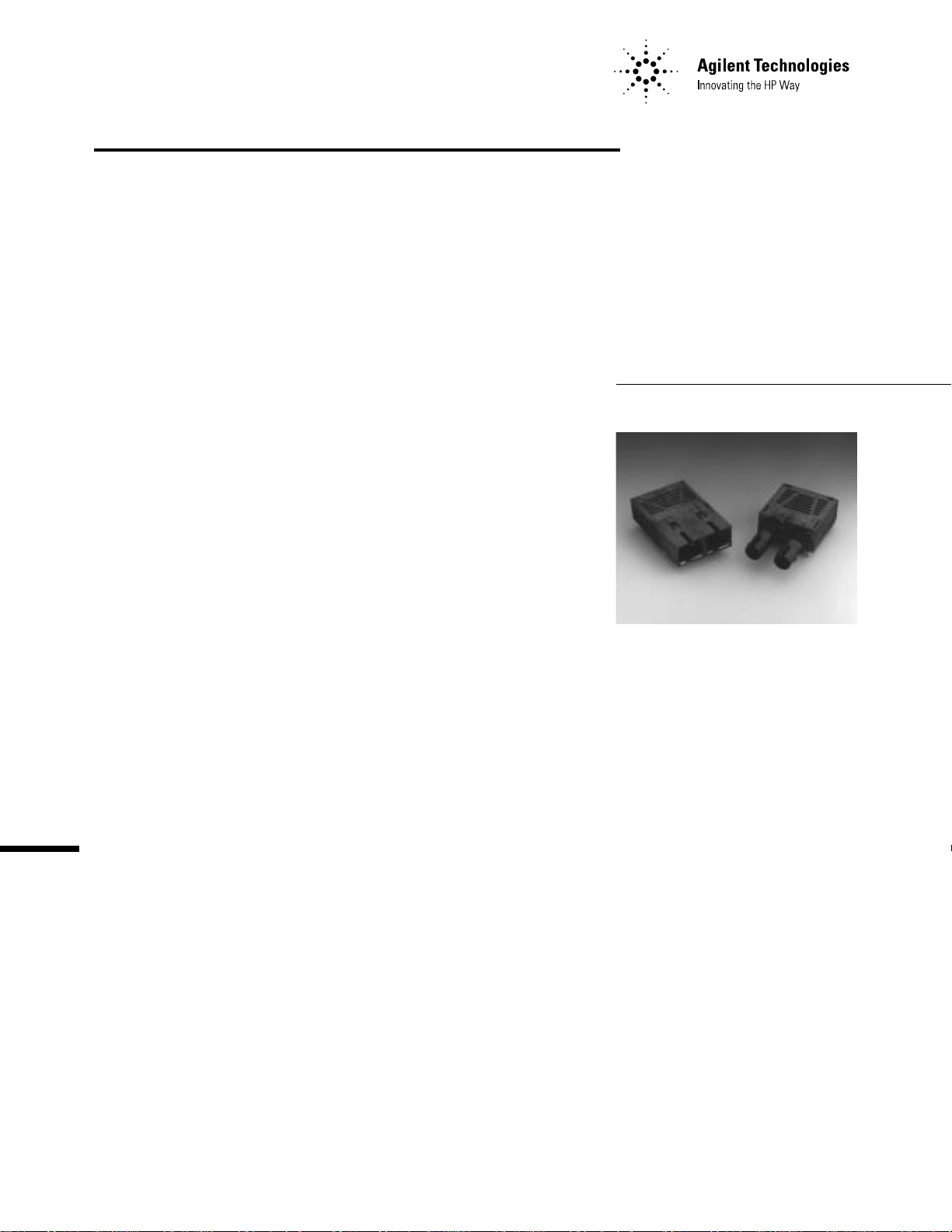
The HFBR-5200 family of transceivers from Agilent Technologies
provide the system designer with
products to implement a range of
solutions for multimode fiber
SONET OC-3 (SDH STM-1)
physical layers for ATM and other
services.
These transceivers are all
supplied in the new industry
standard 1x9 SIP package style
with either a duplex SC or a
duplex ST* connector interface.
ATM 2000 m Backbone Links
The HFBR-5205/-5205T are
1300 nm products with optical
performance compliant with the
SONET STS-3c (OC-3) Physical
Layer Interface Specification. This
physical layer is defined in the
ATM Forum User-Network Interface (UNI) Specification Version
3.0. This document references the
ANSI T1E1.2 specification for the
details of the interface for 2000
meter multimode fiber backbone
links.
Selected versions of these
transceivers may be used to
implement the ATM Forum UNI
Physical Layer Interface at the
155 Mbps/194 MBd rate.
The ATM 100 Mbps/125 MBd
Physical Layer interface is best
implemented with the HFBR-5100
family of FDDI Transceivers
which are specified for use in this
4B/5B encoded physical layer per
the FDDI PMD standard.
HFBR-5203/-5203T
800 nm 300 m
HFBR-5204/-5204T
1300 nm 500 m
HFBR-5205/-5205T
1300 nm 2 km
ATM 500 m Backbone and
Desktop Links
The HFBR-5204/-5204T are 1300
nm products which are similar to
the HFBR-5205/5205T except
that they are intended to provide
a lower cost SONET OC-3 link to
distances up to 500 meters in
62.5/125 µm multimode fiber
optic cables.
Very Low Cost ATM 300 m
Desktop Links
The HFBR-5203/-5203T are very
low cost 800 nm alternatives to
the HFBR-5204/-5204T for
SONET OC-3 links to distances up
to 300 meters in 62.5/125 µm
multimode fiber optic cables.
Transmitter Sections
The transmitter sections of the
HFBR-5204 and HFBR-5205
series utilize 1300 nm InGaAsP
LEDs and the HFBR-5203 series
*ST is a registered trademark of AT&T Lightguide Cable Connectors.
Page 2

2
uses a low cost 800 nm AlGaAs
LED. These LEDs are packaged in
the optical subassembly portion
of the transmitter section. They
are driven by a custom silicon IC
which converts differential PECL
logic signals, ECL referenced
(shifted) to a +5 Volt supply, into
an analog LED drive current.
Receiver Sections
The receiver sections of the
HFBR-5204 and HFBR-5205
series utilize InGaAs PIN photodiodes coupled to a custom
silicon transimpedance preamplifier IC. The HFBR-5203 series
uses the same preamplifier IC in
conjunction with an inexpensive
silicon PIN photodiode. These are
packaged in the optical subassembly portion of the receiver.
These PIN/preamplifier combinations are coupled to a custom
quantizer IC which provides the
final pulse shaping for the logic
output and the Signal Detect
function. The data output is
differential. The signal detect
output is single-ended. Both data
and signal detect outputs are
PECL compatible, ECL referenced
(shifted) to a +5 volt power
supply.
design complies with the
maximum height allowed for the
duplex SC connector over the
entire length of the package.
The optical subassemblies utilize
a high volume assembly process
together with low cost lens
elements which result in a cost
effective building block.
The electrical subassembly consists of a high volume multilayer
printed circuit board on which the
IC chips and various surfacemounted passive circuit elements
are attached.
The package includes internal
shields for the electrical and
optical subassemblies to insure
low EMI emissions and high
immunity to external EMI fields.
The outer housing including the
duplex SC connector or the
duplex ST ports is molded of filled
non-conductive plastic to provide
mechanical strength and electrical
isolation. The solder posts of the
Agilent design are isolated from
the circuit design of the
transceiver and do not require
connection to a ground plane on
the circuit board.
The transceiver is attached to a
printed circuit board with the nine
signal pins and the two solder
posts which exit the bottom of the
housing. The two solder posts
provide the primary mechanical
strength to withstand the loads
imposed on the transceiver by
mating with the duplex or simplex
SC or ST connectored fiber
cables.
Note: The “T” in the product
numbers indicates a transceiver
with a duplex ST connector
receptacle. Product numbers
without a “T” indicate transceivers
with a duplex SC connector
receptacle.
Application Information
The Applications Engineering
group in the Agilent Optical
Communication Division is
available to assist you with the
technical understanding and
design trade-offs associated with
these transceivers. You can contact them through your Agilent
sales representative.
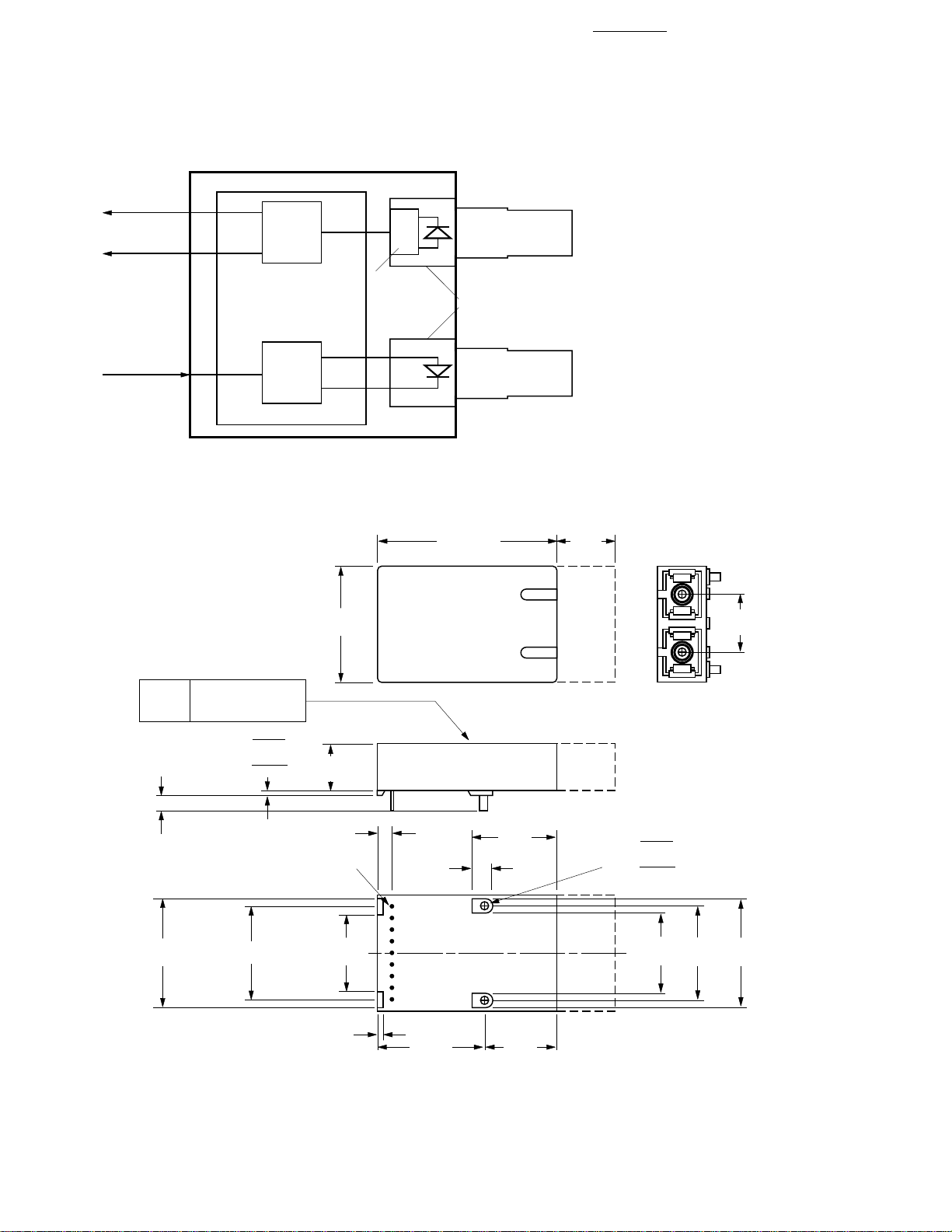
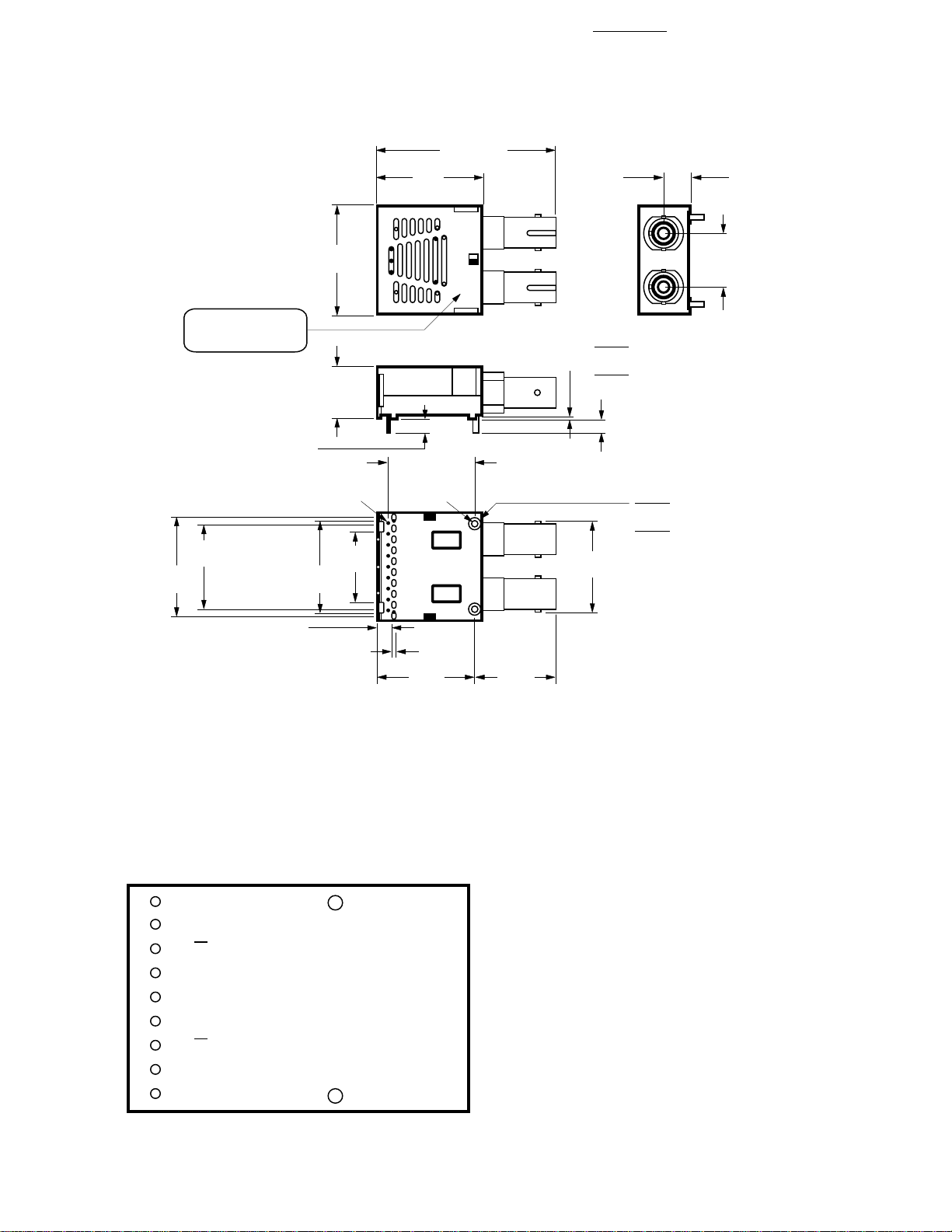
Package
The overall package concept for
the Agilent transceivers consists
of three basic elements; the two
optical subassemblies, an
electrical subassembly, and the
housing as illustrated in the block
diagrams in Figure 1 and
Figure 1a.
The package outline drawing and
pin out are shown in Figures 2,
2a, and 3. The details of this
package outline and pin out are
compliant with the multisource
definition of the 1x9 SIP. The low
profile of the Agilent transceiver
ELECTRICAL SUBASSEMBLY
DIFFERENTIAL
DATA OUT
SINGLE-ENDED
SIGNAL
DETECT OUT
DIFFERENTIAL
DATA IN
Figure 1. Block Diagram.
QUANTIZER IC
DRIVER IC
DUPLEX SC
RECEPTACLE
PIN PHOTODIODE
PREAMP IC
OPTICAL
SUBASSEMBLIES
LED
TOP VIEW
Page 3
3
ELECTRICAL SUBASSEMBLY
DIFFERENTIAL
DATA OUT
SINGLE-ENDED
SIGNAL
DETECT OUT
QUANTIZER IC
DIFFERENTIAL
DATA IN
DRIVER IC
Figure 1a. ST Block Diagram.
TOP VIEW
25.40
(1.000)
PREAMP IC
MAX.
DUPLEX ST
RECEPTACLE
PIN PHOTODIODE
OPTICAL
SUBASSEMBLIES
LED
39.12
MAX.
(1.540)
12.70
(0.500)
AREA
RESERVED
FOR
PROCESS
PLUG
12.70
(0.500)
HFBR-5XXX
DATE CODE (YYWW)
A
SINGAPORE
+ 0.08
0.75
3.30 ± 0.38
(0.130 ± 0.015)
23.55
(0.927)
(0.800)
NOTE 1: THE SOLDER POSTS AND ELECTRICAL PINS ARE PHOSPHOR BRONZE WITH TIN LEAD OVER NICKEL PLATING.
DIMENSIONS ARE IN MILLIMETERS (INCHES).
(0.030
20.32
[8x(2.54/.100)]
- 0.05
+ 0.003
- 0.002
)
0.46
(0.018)
NOTE 1
10.35
(0.407)
2.92
(0.115)
(9x)ø
16.70
(0.657)
0.87
(0.034)
MAX.
23.24
(0.915)
18.52
(0.729)
4.14
(0.163)
15.88
(0.625)
1.27
(0.050
+ 0.25
- 0.05
+ 0.010
- 0.002
NOTE 1
17.32
(0.682)
)
20.32
(0.800)
23.32
(0.918)
Figure 2. Package Outline Drawing.
Page 4
24.8
(0.976)
42
(1.654)
4
MAX.
5.99
(0.236)
HFBR-5103T
DATE CODE (YYWW)
SINGAPORE
20.32
[(8x (2.54/0.100)]
(0.800)
22.86
(0.900)
3.2
(0.126)
3.6
(0.142)
25.4
(1.000)
12.0
(0.471)
φ
(0.022)
NOTE 1
21.4
(0.843)
MAX.
MAX.
0.46
17.4
(0.685)
1.3
(0.051)
20.32
φ
(0.102)
23.38
(0.921)
± 0.38
(± 0.015)
2.6
18.62
(0.733)
+ 0.08
0.5
- 0.05
(0.020)
+ 0.003
(
- 0.002
3.3 ± 0.38
(0.130) (± 0.015)
20.32
(0.800)
(
+ 0.25
- 0.05
+ 0.010
(
- 0.002
12.7
(0.500)
(
NOTE 1: PHOSPHOR BRONZE IS THE BASE MATERIAL FOR THE POSTS & PINS
WITH TIN LEAD OVER NICKEL PLATING.
DIMENSIONS IN MILLIMETERS (INCHES).
Figure 2a. ST Package Outline Drawing.
1 = V
2 = RD
3 = RD
4 = SD
5 = V
6 = V
7 = TD
8 = TD
9 = V
EE
CC
CC
EE
TOP VIEW
N/C
N/C
Figure 3. Pin Out Diagram.
Page 5
5
The following information is
provided to answer some of the
most common questions about
the use of these parts.
Agilent LED technology has
produced 800 nm LED and 1300
nm LED devices with lower aging
characteristics than normally
associated with these technolo-
Transceiver Optical Power
Budget versus Link Length
Optical Power Budget (OPB) is
the available optical power for a
fiber optic link to accommodate
fiber cable losses plus losses due
to in-line connectors, splices,
optical switches, and to provide
margin for link aging and
unplanned losses due to cable
gies in the industry. The industry
convention is 3 dB aging for 800
nm and 1.5 dB aging for 1300 nm
LEDs. The 1300 nm HP LEDs are
specified to experience less than
1 dB of aging over normal
commercial equipment mission
life periods. Contact your Agilent
sales representative for additional
details.
plant reconfiguration or repair.
Figure 4 was generated for the
Figure 4 illustrates the predicted
OPB associated with the three
transceivers series specified in
this data sheet at the Beginning of
Life (BOL). These curves represent the attenuation and chromatic
plus modal dispersion losses
associated with the 62.5/125 µm
and 50/125 µm fiber cables only.
The area under the curves
represents the remaining OPB at
any link length, which is available
for overcoming non-fiber cable
losses.
1300 nm transceivers with an
Agilent fiber optic link model
containing the current industry
conventions for fiber cable
specifications and the draft ANSI
T1E1.2. These optical parameters
are reflected in the guaranteed
performance of the transceiver
specifications in this data sheet.
This same model has been used
extensively in the ANSI and IEEE
committees, including the ANSI
T1E1.2 committee, to establish
the optical performance
requirements for various fiber
12
10
8
HFBR-5203,
6
50/125 µm
4
2
OPTICAL POWER BUDGET (dB)
0
Figure 4. Optical Power Budget vs. Fiber Optic Cable Length.
HFBR-5205, 62.5/125 µm
HFBR-5203,
62.5/125 µm
HFBR-5205,
50/125 µm
HFBR-5204,
62.5/125 µm
HFBR-5204,
50/125 µm
0.5 1.5 2.0 2.5
1.00.3
FIBER OPTIC CABLE LENGTH (km)
optic interface standards. The
cable parameters used come from
the ISO/IEC JTC1/SC 25/WG3
Generic Cabling for Customer
Premises per DIS 11801 document and the EIA/TIA-568-A
Commercial Building
Telecommunications Cabling
Standard per SP-2840.
The HFBR-5203 series 800 nm
transceiver curve in Figure 4 was
generated based on extensive
empirical test data of the 800 nm
transceiver performance. The
curve includes the effect of typical
fiber attenuation, plus receiver
sensitivity loss due to chromatic
and metal dispersion losses
through the fiber.
Transceiver Signaling
Operating Rate Range and BER
Performance
For purposes of definition, the
symbol (Baud) rate, also called
signaling rate, is the reciprocal of
the symbol time. Data rate (bits/
sec) is the symbol rate divided by
the encoding factor used to
encode the data (symbols/bit).
When used in 155 Mbps SONET
OC-3 applications the performance of the 1300 nm transceivers,
HFBR-5204/5205 is guaranteed
to the full conditions listed in
individual product specification
tables.
The transceivers may be used for
other applications at signaling
rates different than 155 Mbps
with some variation in the link
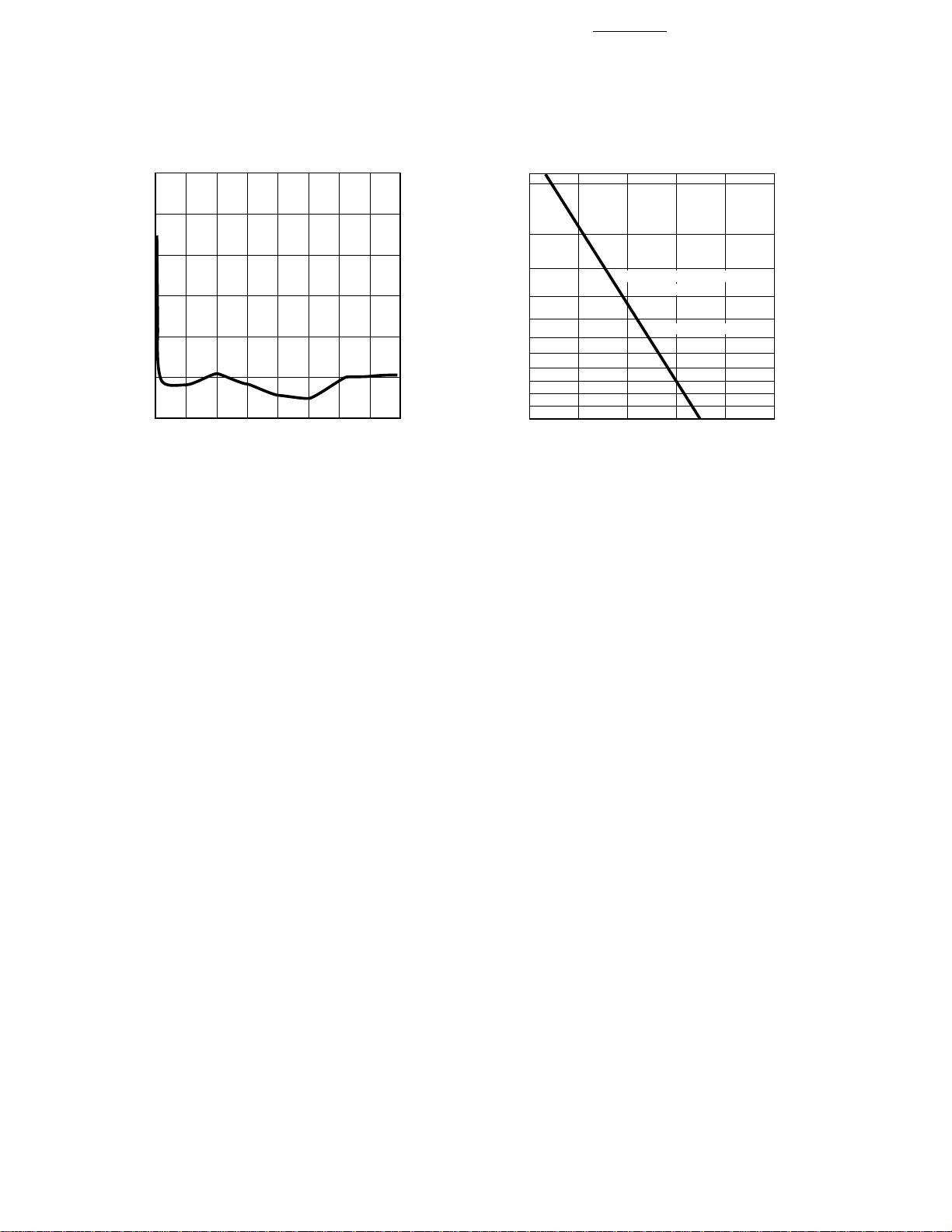
optical power budget. Figure 5
gives an indication of the typical
performance of these products at
different rates.
These transceivers can also be
used for applications which
require different Bit Error Rate
(BER) performance. Figure 6
Page 6
6
2.5
2.0
1.5
1.0
0.5
AT CONSTANT BER (dB)
0
0.5
25 75 100 125
0 200
TRANSCEIVER RELATIVE OPTICAL POWER BUDGET
CONDITIONS:
1. PRBS 2
2. DATA SAMPLED AT CENTER OF DATA SYMBOL.
3. BER = 10
4. TA = 25° C
5. V
6. INPUT OPTICAL RISE/FALL TIMES = 1.0/2.1 ns.
Figure 5. Transceiver Relative Optical Power Budget
at Constant BER vs. Signaling Rate.
50 150
SIGNAL RATE (MBd)
7
-1
-6
= 5 Vdc
CC
175
-2
1 x 10
-3
1 x 10
-4
1 x 10
-5
1 x 10
-6
1 x 10
-7
1 x 10
BIT ERROR RATE
-8
1 x 10
-9
1 x 10
-10
1 x 10
-11
1 x 10
-12
1 x 10
-6 4
-4 2-2
RELATIVE INPUT OPTICAL POWER – dB
CONDITIONS:
1. 155 MBd
2. PRBS 2
3. CENTER OF SYMBOL SAMPLING.
4. T
= 25° C
A
5. V
= 5 Vdc
CC
6. INPUT OPTICAL RISE/FALL TIMES = 1.0/2.1 ns.
Figure 6. Bit Error Rate vs. Relative Receiver Input
Optical Power.
HFBR-5203/5204/5205
SERIES
CENTER OF SYMBOL
7
-1
0
illustrates the typical trade-off
between link BER and the
receivers input optical power
level.
Transceiver Jitter
Performance
The Agilent 1300 nm transceivers
are designed to operate per the
system jitter allocations stated in
Table B1 of Annex B of the draft
ANSI T1E1.2 Revision 3 standard.
The Agilent 1300 nm transmitters
will tolerate the worst case input
electrical jitter allowed in Annex
B without violating the worst case
output optical jitter requirements.
The Agilent 1300 nm receivers
will tolerate the worst case input
optical jitter allowed in Annex B
without violating the worst case
output electrical jitter allowed.
The jitter specifications stated in
the following 1300 nm transceiver
specification tables are derived
from the values in Table B1 of
Annex B. They represent the
worst case jitter contribution that
the transceivers are allowed to
make to the overall system jitter
without violating the Annex B
allocation example. In practice,
the typical contribution of the
Agilent transceivers is well below
these maximum allowed amounts.
Recommended Handling
Precautions
Agilent recommends that normal
static precautions be taken in the
handling and assembly of these
transceivers to prevent damage
which may be induced by
electrostatic discharge (ESD).
The HFBR-5200 series of
transceivers meet MIL-STD-883C
Method 3015.4 Class 2 products.
Care should be used to avoid
shorting the receiver data or
signal detect outputs directly to
ground without proper current
limiting impedance.
Solder and Wash Process
Compatibility
The transceivers are delivered
with protective process plugs
inserted into the duplex SC or
duplex ST connector receptacle.
This process plug protects the
optical subassemblies during
wave solder and aqueous wash
processing and acts as a dust
cover during shipping.
These transceivers are compatible
with either industry standard
wave or hand solder processes.
Shipping Container
The transceiver is packaged in a
shipping container designed to
Page 7

NO INTERNAL CONNECTION NO INTERNAL CONNECTION
HFBR-520X
TOP VIEW
Rx Rx Tx Tx
RD RD SD V
V
EE
123456789
CCVCC
C1 C2
TD TD V
EE
7
V
CC
TERMINATION
AT PHY
DEVICE
INPUTS
R6 R8
NOTES:
THE SPLIT-LOAD TERMINATIONS FOR ECL SIGNALS NEED TO BE LOCATED AT THE INPUT
OF DEVICES RECEIVING THOSE ECL SIGNALS. RECOMMEND 4-LAYER PRINTED CIRCUIT
BOARD WITH 50 OHM MICROSTRIP SIGNAL PATHS BE USED.
R1 = R4 = R6 = R8 = R10 = 130 OHMS.
R2 = R3 = R5 = R7 = R9 = 82 OHMS.
C1 = C2 = C3 = C5 = C6 = 0.1 µF.
C4 = 10 µF.
L1 = L2 = 1 µH COIL OR FERRITE INDUCTOR.
Figure 7. Recommended Decoupling and Termination Circuits.
V
CC
R5 R7
C6
RD RD SD V
protect it from mechanical and
ESD damage during shipment or
storage.
L1 L2
C3 C4
VCC FILTER
AT V
PINS
CC
TRANSCEIVER
R9
R10
CC
with these parts. It is further
recommended that a contiguous
ground plane be provided in the
R2 R3
R1 R4
C5
TERMINATION
AT TRANSCEIVER
INPUTS
TD TD
circuit board directly under the
Board Layout - Decoupling
Circuit and Ground Planes
It is important to take care in the
layout of your circuit board to
achieve optimum performance
from these transceivers. Figure 7
transceiver to provide a low
inductance ground for signal
return current. This recommendation is in keeping with good
high frequency board layout
practices.
provides a good example of a
schematic for a power supply
decoupling circuit that works well
Board Layout - Hole Pattern
The Agilent transceiver complies
with the circuit board “Common
Transceiver Footprint” hole
pattern defined in the original
multisource announcement which
defined the 1x9 package style.
This drawing is reproduced in
Figure 8 with the addition of ANSI
Y14.5M compliant dimensioning
to be used as a guide in the
mechanical layout of your circuit
board.
Page 8

20.32
.800
20.32
.800
(2X)
(9X)
1.9 ± 0.1
ø
.075 ± .004
Ø0.000
0.8 ± 0.1
ø
.032 ± .004
Ø0.000
8
–A–
MA
MA
2.54
(8X)
.100
Figure 8. Recommended Board Layout Hole Pattern.
Board Layout - Art Work
The Applications Engineering
group is developing Gerber file
duplex SC and duplex ST
transceiver packages in relation
to the chassis panel.
art work for a multilayer printed
circuit board layout incorporating
the recommendations above.
Contact your local Agilent sales
representative for details.
Regulatory Compliance
These transceiver products are
intended to enable commercial
system designers to develop
equipment that complies with the
Board Layout - Mechanical
For applications interested in
providing a choice of either a
duplex SC or a duplex ST connector interface, while utilizing
the same pinout on the printed
circuit board, the ST port needs
various international regulations
governing certification of Information Technology Equipment.
See the Regulatory Compliance
Table for details. Additional
information is available from your
Agilent sales representative.
to protrude from the chassis
panel a minimum of 9.53 nm for
sufficient clearance to install the
ST connector.
Electrostatic Discharge (ESD)
There are two design cases in
which immunity to ESD damage
is important.
Please refer to Figure 8a for a
mechanical layout detailing the
recommended location of the
TOP VIEW
The first case is during handling
of the transceiver prior to
mounting it on the circuit board.
It is important to use normal ESD
handling precautions for ESD
sensitive devices. These precautions include using grounded
wrist straps, work benches, and
floor mats in ESD controlled
areas.
The second case to consider is
static discharges to the exterior of
the equipment chassis containing
the transceiver parts. To the
extent that the duplex SC
connector is exposed to the
outside of the equipment chassis
it may be subject to whatever ESD
system level test criteria that the
equipment is intended to meet.
Page 9

9
0.51
0.75
12.0
11.1
9.53
(NOTE 1)
12.09
6.79
42.0
39.12
24.8
Electromagnetic Interference
(EMI)
Most equipment designs utilizing
these high speed transceivers
from Agilent will be required to
meet the requirements of FCC in
the United States, CENELEC
EN55022 (CISPR 22) in Europe
and VCCI in Japan.
25.4
These products are suitable for
use in designs ranging from a
desktop computer with a single
transceiver to a concentrator or
switch product with large number
of transceivers.
In all well-designed chassis, the
two 0.5" holes required for ST
connectors to protrude through,
will provide 4.6 dB more
shielding than one 1.2" duplex SC
rectangular cutout. Thus, in a
25.4
well-designed chassis, the duplex
ST 1x9 transceiver emissions will
be identical to the duplex SC 1x9
transceiver emissions.
NOTE 1: MINIMUM DISTANCE FROM FRONT
OF CONNECTOR TO THE PANEL FACE.
Figure 8a. Recommended Common Mechanical Layout for ST and ST 1x9
Connectored Transceivers.
Immunity
Equipment utilizing these transceivers will be subject to radiofrequency electromagnetic fields
in some environments. These
transceivers have a high immunity
to such fields.
For additional information regarding EMI, susceptibility, ESD and
conducted noise testing procedures and results on the 1x9
transceiver family, please refer to
Applications Note 1075, Testing
and Measuring Electromagnetic Compatibility
Performance of the HFBR510X/-520X Fiber Optic
Transceivers.
Page 10

10
200
180
1.0
160
1.5
140
2.0
t
– TRANSMITTER
2.5
120
SPECTRAL WIDTH (FWHM) –nm
∆λ – TRANSMITTER OUTPUT OPTICAL
3.0
100
1260
1280 1300 1320
λC – TRANSMITTER OUTPUT OPTICAL
CENTER WAVELENGTH –nm
HFBR-5205 TRANSMITTER TEST RESULTS
OF λ
, ∆λ AND t
C
COMPLY WITH THE ALLOWED SPECTRAL WIDTH
AS A FUNCTION OF CENTER WAVELENGTH FOR
VARIOUS RISE AND FALL TIMES.
r/f
OUTPUT OPTICAL
RISE/FALL TIMES – ns
ARE CORRELATED AND
r/f
3.0
13601340
Figure 9. Transmitter Output Optical Spectral Width
(FWHM) vs. Transmitter Output Optical Center
Wavelength and Rise/Fall Times.
5
4
3
2
1
RELATIVE INPUT OPTICAL POWER (dB)
0
-3 -1 0 1
CONDITIONS:
1.T
A
2. V
3. INPUT OPTICAL RISE/FALL TIMES = 1.0/2.1 ns.
4. INPUT OPTICAL POWER IS NORMALIZED TO
CENTER OF DATA SYMBOL.
5. NOTE 16 AND 17 APPLY.
HFBR-5203/-5204/-5205
SERIES
-2 2
EYE SAMPLING TIME POSITION (ns)
= 25° C
= 5 Vdc
CC
3
Figure 10. Relative Input Optical Power vs. Eye Sampling
Time Position.
Regulatory Compliance Table
Feature Test Method Performance
Electrostatic Discharge MIL-STD-883C Meets Class 2 (2000 to 3999 Volts)
(ESD) to the Electrical Method 3015.4 Withstand up to 2200 V applied between electrical
Pins pins.
Electrostatic Discharge Variation of Typically withstand at least 25 kV without damage
(ESD) to the Duplex SC IEC 801-2 when the Duplex SC Connector Receptacle
Receptacle is contacted by a Human Body Model probe.
Electromagnetic FCC Class B Transceivers typically provide a 13 dB margin
Interference (EMI) CENELEC EN55022 (with duplex SC receptacle) or a 9 dB margin
Class B (CISPR 22B) (with duplex ST receptacles) to the noted
VCCI Class 2 standard limits when tested at a certified test
range with the transceiver mounted to a circuit
card without a chassis enclosure.
Immunity Variation of IEC 801-3 Typically show no measurable effect from a
10 V/m field swept from 10 to 450 MHz applied
to the transceiver when mounted to a circuit card
without a chassis enclosure.
Page 11

11
Transceiver Reliability
and Performance
Qualification Data
The 1 x 9 transceivers have
passed Agilent reliability and
performance qualification testing
and are undergoing ongoing
quality monitoring. Details are
available from your Agilent sales
representative.
These transceivers are
manufactured at the Agilent
Singapore location which is an
ISO 9002 certified facility.
Ordering Information
The HFBR-5204/-5204T and
HFBR-5205/-5205T 1300 nm
products and the HFBR-5203/
-5203T 800 transceivers are
available for production orders
through the Agilent Component
Field Sales Offices and Authorized
Distributors world wide.
Applications Support
Materials
Contact your local Agilent
Component Field Sales Office for
information on how to obtain PCB
Layouts, Test Boards and demo
boards for the 1x9 transceivers.
Evaluation Kits
Agilent has available three
evaluation kits for the 1x9
transceivers. The purpose of these
kits is to provide the necessary
materials to evaluate the performance of the HFBR-520X family in
a pre-existing 1x13 or 2x11
pinout system design configuration or when connectored to
various test equipment.
1. HFBR-0305 – ATM Evaluation
Kit:
This kit consists of one HFBR5205, one 1 x 13 to 1 x 9 pin
out adapter card, and one three
meter duplex SC to duplex ST
connectored 62.5/125 µm fiber
optic cable.
2. HFBR-0303 – FDDI Evaluation
Kit:
This kit consists of one HFBR5103, one 2 x 11 to 1 x 9 pin out
adapter card, one 1 x 13 to 1 x 9
pin out adapter card, and one
three meter duplex SC to MIC/
Receptacle connectored 62.5/
125 µm fiber optic cable.
3. HFBR-0319 – Evaluation Test
Fixture Board:
This test fixture converts +5 V
ECL 1x9 transceivers to –5 V
ECL BNC Coax Connections so
that direct connections to
industry standard fiber optic test
equipment can be accomplished.
Accessory Duplex SC
Connectored Cable Assemblies
Agilent recommends for optimal
coupling the use of flexible-body
duplex SC connectored cable.
Page 12

HFBR-5203, -5204, and -5205 Series
Absolute Maximum Ratings
Parameter Symbol Min. Typ. Max. Unit Reference
Storage Temperature T
Lead Soldering Temperature T
Lead Soldering Time t
Supply Voltage V
Data Input Voltage V
Differential Input Voltage V
Output Current I
S
SOLD
SOLD
CC
I
D
O
HFBR-5203, -5204, and -5205 Series
Recommended Operating Conditions
12
-40 100 °C
260 °C
10 sec.
-0.5 7.0 V
-0.5 V
CC
1.4 V Note 1
50 mA
V
Parameter Symbol Min. Typ. Max. Unit Reference
Ambient Operating Temperature T
Supply Voltage V
Data Input Voltage - Low V
Data Input Voltage - High V
IL
IH
Data and Signal Detect Output Load R
A
CC
- V
- V
070°C
4.75 5.25 V
-1.810 -1.475 V
CC
-1.165 -0.880 V
CC
L
50 Ω Note 2
Page 13

13
Agilent offers two such
compatible Duplex SC connectored jumper cable assemblies to
assist you in the evaluation of
these transceiver products. These
2. HFBR-BKD010
A duplex cable 10 meters long
assembled with 62.5/125 µm fiber
and Duplex SC connector plugs
on both ends.
cables may be purchased from
Agilent with the following part
numbers.
Accessory Duplex ST
Connectored Cable Assemblies
Agilent recommends the use of
1. HFBR-BKD001
A duplex cable 1 meter long
assembled with 62.5/125 µm fiber
Duplex Push-Pull ST connectored
cable for optimal repeatibility of
the optical power coupling.
and Duplex SC connector plugs
on both ends.
HFBR-5203, -5204 and -5205 Series
Transmitter Electrical Characteristics
(TA = 0°C to 70°C, VCC = 4.75 V to 5.25 V)
Parameter Symbol Min. Typ. Max. Unit Reference
Supply Current I
Power Dissipation P
Data Input Current - Low I
Data Input Current - High I
CC
DISS
IL
IH
145 185 mA Note 3
0.76 0.97 W
-350 0 µA
14 350 µA
HFBR-5203, -5204 and -5205 Series
Receiver Electrical Characteristics
(TA = 0°C to 70°C, VCC = 4.75 V to 5.25 V)
Parameter Symbol Min. Typ. Max. Unit Reference
Supply Current I
Power Dissipation P
Data Output Voltage - Low VOL - V
Data Output Voltage - High VOH - V
Data Output Rise Time t
Data Output Fall Time t
Signal Detect Output Voltage - Low VOL - V
Signal Detect Output Voltage - High VOH - V
Signal Detect Output Rise Time t
Signal Detect Output Fall Time t
CC
DISS
82 145 mA Note 4
0.3 0.5 W Note 5
-1.840 -1.620 V Note 6
CC
-1.045 -0.880 V Note 6
CC
r
f
CC
CC
r
f
0.35 2.2 ns Note 7
0.35 2.2 ns Note 7
-1.840 -1.620 V Note 6
-1.045 -0.880 V Note 6
0.35 2.2 ns Note 7
0.35 2.2 ns Note 7
Page 14

Agilent offers two such
compatible duplex Push-Pull ST
connectored jumper cable
assemblies to assist you in your
evaluation of these products.
These cables may be purchased
from Agilent with the following
part numbers.
1. HFBR-XXX001
A duplex cable 1 meter long
assembled with 62.5/125 µm fiber
and Duplex Push-Pull ST
connector plugs on both ends.
2. HFBR-XXX010
A duplex cable 10 meters long
assembled with 62.5/125 µm fiber
and Duplex Push-Pull ST
connector plugs on both ends.
14
Page 15

15
HFBR-5203/-5203T
Transmitter Optical Characteristics
(TA = 0°C to 70°C, VCC = 4.75 V to 5.25 V)
Parameter Symbol Min. Typ. Max. Unit Reference
Output Optical Power BOL P
O
62.5/125 µm, NA = 0.275 Fiber EOL -20
Output Optical Power BOL P
O
50/125 µm, NA = 0.20 Fiber EOL -23.8
Optical Extinction Ratio 0.01 % Note 10
Output Optical Power at PO (“0”) -45 dBm avg. Note 11
Logic “0” State
Center Wavelength λ
C
Spectral Width - FWHM ∆λ 100 nm Note 12
- nm RMS 43 nm RMS
Optical Rise Time t
Optical Fall Time t
r
f
Systematic Jitter Contributed SJ 1.7 ns p-p Note 14
by the Transmitter
Random Jitter Contributed RJ 0.52 ns p-p Note 15
by the Transmitter
-17 -12 dBm avg. Note 9
-20.8 -12 dBm avg. Note 9
-40 dB
800 900 nm
4.5 ns Note 13
4.5 ns Note 13
HFBR-5203/-5203T
Receiver Optical and Electrical Characteristics
(TA = 0°C to 70°C, VCC = 4.75 V to 5.25 V)
Parameter Symbol Min. Typ. Max. Unit Reference
Input Optical Power P
Minimum at Window Edge
Output Optical Power P
Minimum at Eye Center
Input Optical Power Maximum P
Operating Wavelength λ 800 900 nm
Systematic Jitter Contributed SJ 0.9 ns p-p Note 18
by the Receiver
Random Jitter Contributed RJ 1.16 ns p-p Note 19
by the Receiver
Signal Detect - Asserted P
Signal Detect - Deasserted P
Signal Detect - Hysteresis PA - P
Signal Detect Assert Time 0 100 µs Note 22
(off to on)
Signal Detect Deassert Time 0 350 µs Note 23
(on to off)
(W) -26 dBm avg. Note 16
IN Min.
(C) -27 dBm avg. Note 17
IN Min.
IN Max.
A
D
D
-12 dBm avg. Note 16
PD + 1.5 dB -28 dBm avg. Note 20
-45 PA-1.5 dBm avg. Note 21
1.5 dB
Page 16

16
HFBR-5204/-5204T
Transmitter Optical Characteristics
(TA = 0°C to 70°C, VCC = 4.75 V to 5.25 V)
Parameter Symbol Min. Typ. Max. Unit Reference
Output Optical Power BOL P
O
62.5/125 µm, NA = 0.275 Fiber EOL -22
Output Optical Power BOL P
O
50/125 µm, NA = 0.20 Fiber EOL -25.5
Optical Extinction Ratio 0.03 % Note 10
Output Optical Power at PO (“0”) -45 dBm avg. Note 11
Logic “0” State
Center Wavelength λ
C
Spectral Width - FWHM ∆λ 250 nm Note 12
- nm RMS 107 nm RMS
Optical Rise Time t
Optical Fall Time t
r
f
Systematic Jitter Contributed SJ 0.04 1.2 ns p-p Note 14
by the Transmitter
Random Jitter Contributed RJ 0 0.52 ns p-p Note 15
by the Transmitter
-21 -14 dBm avg. Note 8
-24.5 -14 dBm avg. Note 8
-35 dB
1270 1310 1380 nm
4 ns Note 13
4 ns Note 13
HFBR-5204/-5204T
Receiver Optical and Electrical Characteristics
(TA = 0°C to 70°C, VCC = 4.75 V to 5.25 V)
Parameter Symbol Min. Typ. Max. Unit Reference
Input Optical Power P
Minimum at Window Edge Figure 10
Input Optical Power P
Minimum at Eye Center Figure 10
Input Optical Power Maximum P
Systematic Jitter Contributed SJ 0.2 1.2 ns p-p Note 18
by the Receiver
Random Jitter Contributed RJ 1 1.91 ns p-p Note 19
by the Receiver
Operating Wavelength λ 1270 1380 nm
Signal Detect - Asserted P
Signal Detect - Deasserted P
Signal Detect - Hysteresis PA - P
Signal Detect Assert Time 0 55 100 µs Note 22
(off to on)
Signal Detect Deassert Time 0 110 350 µs Note 23
(on to off)
(W) -29 dBm avg. Note 16
IN Min.
(C) -30 dBm avg. Note 17
IN Min.
IN Max.
A
D
D
-14 dBm avg. Note 16
PD + 1.5 dB -31 dBm avg. Note 20
-45 dBm avg. Note 21
1.5 dB
Page 17

17
HFBR-5205/-5205T
Transmitter Optical Characteristics
(TA = 0°C to 70°C, VCC = 4.75 V to 5.25 V)
Parameter Symbol Min. Typ. Max. Unit Reference
Output Optical Power BOL P
O
62.5/125 µm, NA = 0.275 Fiber EOL -20
Output Optical Power BOL P
O
50/125 µm, NA = 0.20 Fiber EOL -23.5
Optical Extinction Ratio 0.001 0.03 % Note 10
Output Optical Power at PO ("0") -45 dBm avg. Note 11
Logic "0" State
Center Wavelength λ
C
Spectral Width - FWHM ∆λ 137 nm Note 24
- nm RMS 58 nm RMS Figure 9
Optical Rise Time t
Optical Fall Time t
r
f
Systematic Jitter Contributed SJ 0.04 1.2 ns p-p Note 14
by the Transmitter
Random Jitter Contributed RJ 0 0.52 ns p-p Note 15
by the Transmitter
-19 -14 dBm avg. Note 9
-22.5 -14 dBm avg. Note 9
-50 -35 dB
1270 1310 1380 nm Note 24
Figure 9
0.6 1.0 3.0 ns Note 12, 24
Figure 9
0.6 2.1 3.0 ns Note 12, 24
Figure 9
Page 18

18
HFBR-5205/-5205T
Receiver Optical and Electrical Characteristics
(TA = 0°C to 70°C, VCC = 4.75 V to 5.25 V)
Parameter Symbol Min. Typ. Max. Unit Reference
Input Optical Power P
Minimum at Window Edge Figure 10
Input Optical Power P
Minimum at Eye Center Figure 10
Input Optical Power Maximum P
Operating Wavelength λ 1260 1360 nm
Systematic Jitter Contributed SJ 0.2 1.2 ns p-p Note 18
by the Receiver
Random Jitter Contributed RJ 1 1.91 ns p-p Note 19
by the Receiver
Signal Detect - Asserted P
Signal Detect - Deasserted P
Signal Detect - Hysteresis PA - P
Signal Detect Assert Time 0 55 100 µs Note 22
(off to on)
Signal Detect Deassert Time 0 110 350 µs Note 23
(on to off)
(W) -30 dBm avg. Note 16
IN Min.
(C) -31 dBm avg. Note 17
IN Min.
IN Max.
A
D
D
-14 dBm avg. Note 16
PD + 1.5 dB -31 dBm avg. Note 20
-45 dBm avg. Note 21
1.5 dB
Notes:
1. This is the maximum voltage that
can be applied across the Differential
Transmitter Data Inputs to prevent
damage to the input ESD protection
circuit.
2. The outputs are terminated with
50 Ω connected to VCC -2 V.
3. The power supply current needed to
operate the transmitter is provided
to differential ECL circuitry. This
circuitry maintains a nearly constant current flow from the power
supply. Constant current operation
helps to prevent unwanted electrical
noise from being generated and
conducted or emitted to neighboring
circuitry.
4. This value is measured with the
outputs terminated into 50 Ω
connected to VCC -2 V and an Input
Optical Power level of -14 dBm
average.
5. The power dissipation value is the
power dissipated in the receiver
itself. Power dissipation is calculated as the sum of the products of
supply voltage and currents, minus
the sum of the products of the output
voltages and currents.
6. This value is measured with respect
to VCC with the output terminated
into 50 Ω connected to VCC -2 V.
7. The output rise and fall times are
measured between 20% and 80%
levels with the output connected to
VCC -2 V through 50 Ω.
8. These optical power values are
measured with the following
conditions:
• The Beginning of Life (BOL) to
the End of Life (EOL) optical
power degradation is typically
1.5 dB per the industry convention for long wavelength LEDs.
The actual degradation observed
in Agilent’s 1300 nm LED products
is <1 dB, as specified in this
datasheet.
• Over the specified operating voltage
and temperature ranges.
• With 25 MBd (12.5 MHz square-
wave) input signal.
• At the end of one meter of noted
optical fiber with cladding modes
removed.
The average power value can be
converted to a peak power value by
adding 3 dB. Higher output optical
power transmitters are available on
special request.
9. The same comments of note 9 apply
except that industry convention for
short wavelength LED (800 nm)
aging is 3 dB. This value for Output
Optical Power will provide a
minimum 6 dB optical power budget
at the EOL, which will provide at
least 150 meter link lengths with
margin left over for overcoming
normal passive losses, such as inline connectors, in the cable plant.
The actual degradation observed in
normal commercial environments
will be considerably less than this
amount with Agilent’s 800 nm LED
products. Please consult with your
local Agilent sales representative for
further details.
10. The Extinction Ratio is a measure of
the modulation depth of the optical
signal. The data “0” output optical
power is compared to the data “1”
peak output optical power and
Page 19

19
expressed as a percentage. With the
transmitter driven by a 25 MBd
(12.5 MHz square-wave) input
signal, the average optical power is
measured. The data “1” peak power
is then calculated by adding 3dB to
the measured average optical power.
The data “0” output optical power is
found by measuring the optical
power when the transmitter is
driven by a logic “0” input. The
extinction ratio is the ratio of the
optical power at the “0” level
compared to the optical power at the
“1” level expressed as a percentage
or in decibels.
11. The transmitter will provide this low
level of Output Optical Power when
driven by a logic “0” input. This can
be useful in link troubleshooting.
12. The relationship between Full Width
Half Maximum and RMS values for
Spectral Width is derived from the
assumption of a Gaussian shaped
spectrum which results in a 2.35 X
RMS = FWHM relationship.
13. The optical rise and fall times are
measured from 10% to 90% when
the transmitter is driven by a 25
MBd (12.5 MHz square-wave) input
signal. The ANSI T1E1.2 committee
has designated the possibility of
defining an eye pattern mask for the
transmitter optical output as an
item for further study. Agilent will
incorporate this requirement into
the specifications for these products
if it is defined. The HFBR-5204 and
HFBR-5205 products typically
comply with the template requirements of CCITT (now ITU-T) G.957
Section 3.2.5, Figure 2 for the STM1 rate, excluding the optical receiver
filter normally associated with
single mode fiber measurements
which is the likely source for the
ANSI T1E1.2 committee to follow in
this matter.
14. Systematic Jitter contributed by the
transmitter is defined as the combination of Duty Cycle Distortion
and Data Dependent Jitter.
Systematic Jitter is measured at
50% threshold using a 155.52 MBd
(77.5 MHz square-wave), 27 - 1
psuedorandom data pattern input
signal.
15. Random Jitter contributed by the
transmitter is specified with a
155.52 MBd (77.5 MHz squarewave) input signal.
16. This specification is intended to
indicate the performance of the
receiver section of the transceiver
when Input Optical Power signal
characteristics are present per the
following definitions. The Input
Optical Power dynamic range from
the minimum level (with a window
time-width) to the maximum level is
the range over which the receiver is
guaranteed to provide output data
with a Bit Error Ratio (BER) better
than or equal to 1 x 10
• At the Beginning of Life (BOL)
• Over the specified operating
temperature and voltage ranges
• Input is a 155.52 MBd, 223 - 1
PRBS data pattern with 72 “1”s
and 72 “0”s inserted per the
CCITT (now ITU-T) recommendation G.958 Appendix I.
• Receiver data window time-width
is 1.23 ns or greater for the clock
recovery circuit to operate in. The
actual test data window timewidth is set to simulate the effect
of worst case optical input jitter
based on the transmitter jitter
values from the specification
tables. The test window timewidths are as follows: HFBR-5203
is 4.4ns, HFBR-5205 and HFBR5204 are 3.32 ns.
-10
.
• Transmitter operating with a
155.52 MBd, 77.5 MHz squarewave, input signal to simulate
any cross-talk present between
the transmitter and receiver
sections of the transceiver.
17. All conditions of Note 16 apply except
that the measurement is made at
the center of the symbol with no
window time-width.
18. Systematic Jitter contributed by the
receiver is defined as the combination of Duty Cycle Distortion and
Data Dependent Jitter. Systematic
Jitter is measured at 50% threshold
using a 155.52 MBd (77.5 MHz
square-wave), 27 - 1 psuedorandom
data pattern input signal.
19. Random Jitter contributed by the
receiver is specified with a 155.52
MBd (77.5 MHz square-wave) input
signal.
20. This value is measured during the
transition from low to high levels of
input optical power.
21. This value is measured during the
transition from high to low levels of
input optical power.
22. The Signal Detect output shall be
asserted within 100 µs after a step
increase of the Input Optical Power.
23. Signal detect output shall be deasserted within 350 µs after a step
decrease in the Input Optical Power.
24. The HFBR-5205 transceiver
complies with the requirements for
the tradeoffs between center wavelength, spectral width, and rise/fall
times shown in Figure 9. This figure
is derived from the FDDI PMD
standard (ISO/IEC 9314-3 : 1990
and ANSI X3.166 - 1990) per the
description in ANSI T1E1.2 Revision
3. The interpretation of this figure is
that values of Center Wavelength
and Spectral Width must lie along
the appropriate Optical Rise/Fall
Time curve.
Page 20

www.semiconductor.agilent.com
Data subject to change.
Copyright © 1999 Agilent Technologies, Inc.
Obsoletes 5963-5774E (2/95)
5965-9729E (11/99)
 Loading...