

Page 1

Agilent HDMP-3001
Ethernet over SONET Mapper IC
Device Specification
Data Sheet
Table of Contents
1. Introduction............................................................................................... 5
1.1 Internal Functional Blocks .............................................................. 5
1.2 HDMP-3001 Features List ................................................................ 5
1.3 Applications ....................................................................................... 6
1.4 Benefits............................................................................................... 6
1.5 Interfaces............................................................................................ 6
1.6 Data Processing................................................................................. 6
2. Pinout ......................................................................................................... 7
2.1 Pin Assignments ................................................................................ 7
2.2 Pin Descriptions ................................................................................ 8
2.3 I/O Buffer Types .............................................................................. 16
3. Functional Description .......................................................................... 17
3.1 Introduction ..................................................................................... 17
3.2 Interface Descriptions.................................................................... 17
3.2.1 Microprocessor Interface ....................................................... 17
3.2.2 MII Management Interface .................................................... 17
3.2.3 EEPROM Interface .................................................................. 17
3.2.4 MII Interface............................................................................. 17
3.2.5 SONET/SDH Interface............................................................. 18
3.3 Initialization ..................................................................................... 18
3.3.1 Hardware reset......................................................................... 18
3.3.2 Software Reset ......................................................................... 18
3.3.3 Software State Machine Reset ............................................... 18
3.4 Bit Order........................................................................................... 18
3.4.1 GFP Mode ................................................................................. 18
3.4.2 LAPS Mode ............................................................................... 19
3.5 Performance Monitoring................................................................ 19
3.6 Test.................................................................................................... 20
3.6.1 Loopbacks................................................................................. 20
3.6.2 JTAG .......................................................................................... 21
3.7 Interrupts.......................................................................................... 21
3.7.1 Interrupt Driven Mode ........................................................... 21
3.7.2 Polled Mode.............................................................................. 21
3.7.3 Interrupt Sources..................................................................... 21
3.7.4 APS_INTB ................................................................................. 22
3.8 Data Processing............................................................................... 22
3.8.1 LAPS Processing ...................................................................... 22
3.8.2 GFP Processing........................................................................ 23
Page 2

3.9 SONET/SDH Processing................................................................. 24
3.9.1 Transmit SONET/SDH Processing Overview ...................... 24
3.9.2 Receive SONET/SDH Processing Overview ........................ 25
3.9.3 Transmit SONET/SDH Processing Details........................... 25
3.9.4 Receive SONET/SDH Processing Details............................. 30
4. Application Information ........................................................................ 38
4.1 Chip setup and configuration ........................................................ 38
4.1.1 EEPROM Detection................................................................. 38
4.2 Configurations ................................................................................. 38
4.2.1 PHY and MAC mode ................................................................ 38
4.2.2 SDH and SONET mode ........................................................... 38
4.2.3 LAPS and GFP mode ............................................................... 38
4.2.4 INT Pin Configuration............................................................. 38
4.3 Firmware and System Design Information ................................. 40
4.3.1 Board level pull-ups and pull-downs.................................... 40
4.3.2 Motorola MPC860 Microprocessor Interface ...................... 40
4.3.3 MII Interface............................................................................. 41
4.3.4 EEPROM Interface .................................................................. 41
5. Register Definitions............................................................................... 42
5.1 MII Management Register Map .................................................... 42
5.2 Chip Register Map........................................................................... 44
5.3 SONET/SDH Transmit Registers................................................... 56
5.4 SONET/SDH Receive Registers..................................................... 61
5.5 Ethernet Transmit Registers ......................................................... 79
5.6 Ethernet Receive Registers ........................................................... 88
6. Package Specification .......................................................................... 104
7. Electrical and Thermal Specifications............................................... 107
7.1 Technology..................................................................................... 107
7.2 Maximum Ratings ......................................................................... 107
7.3 Thermal Characteristics............................................................... 107
7.4 DC Characteristics........................................................................ 108
7.5 AC Electrical Characteristics ...................................................... 108
7.5.1 General AC Specifications.................................................... 108
7.5.2 MII Specifications.................................................................. 109
8. Timing Diagrams.................................................................................. 110
8.1 Microprocessor Bus Timing - Write Cycle................................. 110
8.2 Microprocessor Bus Timing - Read Cycle ................................. 111
8.3 Microprocessor Bus Timing Table. ............................................ 112
8.4 Line Interface Receive and Transmit Timing............................ 112
8.5 TOH Interface E1/E2/F1 Transmit Timing................................. 113
8.6 TOH Interface E1/E2/F1 Receive Timing................................... 114
8.7 DCC Interface Transmit Timing.................................................. 114
8.8 DCC Interface Receive Timing.................................................... 115
8.9 JTAG Interface Timing ................................................................. 115
8.10 Reset specification..................................................................... 116
8.11 MII Timing................................................................................... 116
8.12 MDIO Port Timing...................................................................... 117
8.13 EEPROM Port Timing ................................................................ 118
8.14 In Frame Declaration................................................................. 118
9. Applicable Documents ......................................................................... 124
2
Page 3

List of Figures
Figure 1. Functional Block Diagram ......................................................... 5
Figure 2. HDMP-3001 applications ............................................................6
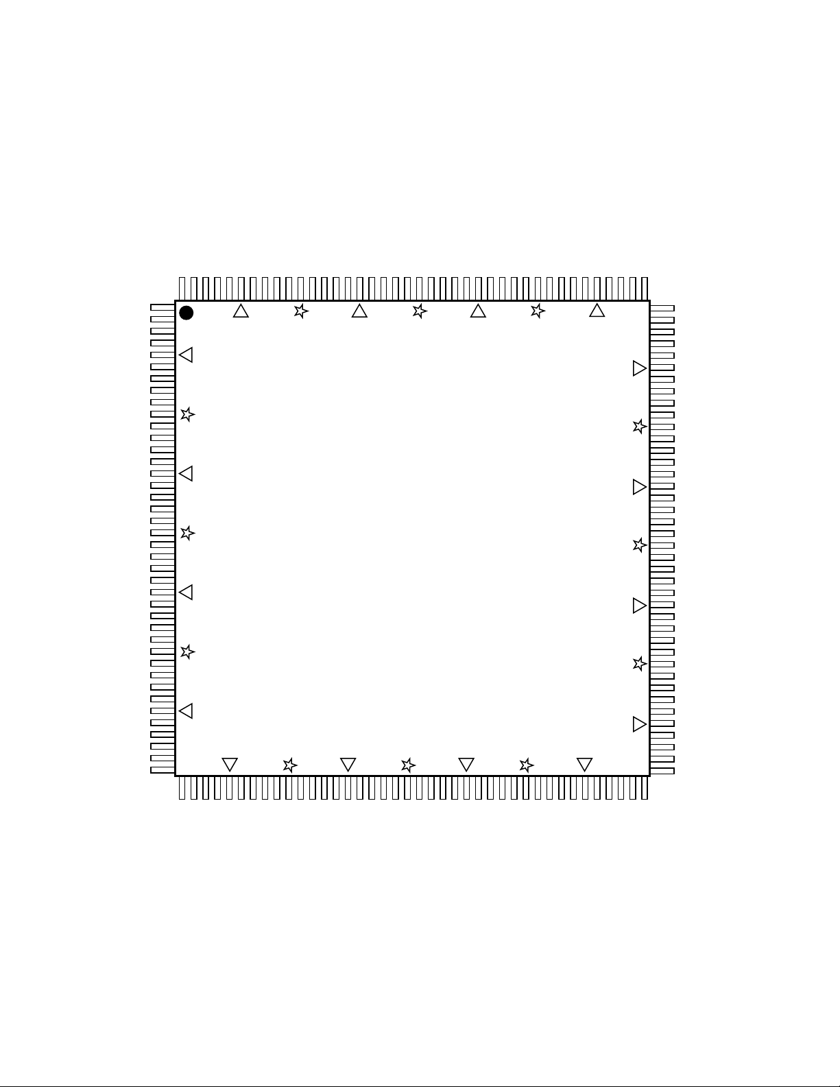
Figure 3. HDMP-3001 pin assignments .....................................................7
Figure 4. GFP Payload Bit Order ............................................................. 18
Figure 5. GFP FCS Bit Order....................................................................18
Figure 6. LAPS Payload Bit Order ...........................................................19
Figure 7. LAPS FCS Bit Order .................................................................. 19
Figure 8. Loopbacks ..................................................................................20
Figure 9. An Ethernet MAC frame ........................................................... 22
Figure 10. The format of a LAPS frame with a MAC payload..............22
Figure 11. The GFP frame......................................................................... 24
Figure 12. The structure of the SONET STS-3c SPE and SDH VC-4... 25
Figure 13. STS-3c SPE or VC-4 Structure ...............................................25
Figure 14. Pointer Byte Fields.................................................................. 29
Figure 15. Pointer Processing ..................................................................33
Figure 16. Pointer tracking algorithm..................................................... 33
Figure 17. Functional block of SONET framer scrambler ................... 36
Figure 18. HDMP-3001 connecting to a MAC......................................... 38
Figure 19. HDMP-3001 connecting to a PHY.......................................... 38
Figure 20. Mode = 00, O/D (Default) ...................................................... 39
Figure 21. Mode = 01, O/S.........................................................................39
Figure 22. Mode = 10, Always Enabled, Active-0 ..................................39
Figure 23. Mode = 11, Always Enabled, Active-1 ..................................39
Figure 24. Package Marking ...................................................................104
Figure 25. Top View of Package ............................................................ 104
Figure 26. Bottom View of Package ......................................................105
Figure 27. Side View of Package........................................................... 105
Figure 28. Detailed View of Pin ............................................................. 105
Figure 29. Microprocessor Write Cycle Timing................................... 110
Figure 30. Microprocessor Read Cycle Timing ................................... 111
Figure 31. Line Interface Transmit Timing...........................................112
Figure 32. Line Interface Receive Timing.............................................113
Figure 33. TOH Interface E1/E2/F1 Transmit Timing......................... 113
Figure 34. TOH Interface E1/E2/F1 Receive Timing...........................114
Figure 35. DCC Interface Transmit Timing .......................................... 114
Figure 36. DCC Interface Receive Timing ............................................ 115
Figure 37. JTAG Interface Timing ......................................................... 115
Figure 38. MII timing as defined by IEEE 802.3 ..................................116
Figure 39. In Frame Declaration............................................................ 118
Figure 40. Out of Frame Declaration ................................................... 119
Figure 41. Loss of Frame Declaration/Removal ..................................119
Figure 42. Line AIS and Line RDI Declaration/Removal ....................119
Figure 43. Transmit Overhead Clock and Data Alignment ................ 120
Figure 44. Receive Overhead Clock and Data Alignment ..................121
Figure 45. Transmit Data Link Clock and Data Alignment ................ 122
Figure 46. Receive Data Link Clock and Data Alignment .................. 123
3
Page 4

List of Tables
Table 1. Line Side Interface Pins Description........................................... 8
Table 2. MII Interface Pins Description..................................................... 9
Table 3. Transport Overhead Pins Description ...................................... 10
Table 4. Microprocessor Interface Pins Description ............................. 12
Table 5. JTAG Interface Pins Description ............................................... 13
Table 6. Two-Wire EEPROM Interface Pins Description...................... 14
Table 7. Miscellaneous Pins Description................................................. 14
Table 8. Buffer types .................................................................................. 16
Table 9. JTAG pins...................................................................................... 21
Table 10. JTAG instructions supported ................................................... 21
Table 11. Path RDI bit values .................................................................... 27
Table 12. STS-3c/STM-1 TOH/SOH ........................................................... 28
Table 13. Pointer Processing..................................................................... 34
Table 14. Pointer Tracking ........................................................................ 34
Table 15. INT Pin Configuration ............................................................... 39
Table 16. Pin Connections – MPC860 ...................................................... 40
Table 17. Pin Connections – MII Interface. ............................................. 41
Table 18. MII Management Register Map ................................................ 42
Table 19. HDMP-3001 Register Map ......................................................... 44
Table 20. G1 values ..................................................................................... 59
Table 21. STS-3c/STM-1 Configuration for
RX_FRAME_POSITION [3:0] .......................................................... 64
Table 22. Package Dimensions ............................................................... 106
Table 23. Absolute Maximum Ratings ................................................... 107
Table 24. Operating Conditions .............................................................. 107
Table 25. Thermal Performance ............................................................. 107
Table 26. DC Electrical Characteristics................................................. 108
Table 27. Power Dissipation.................................................................... 108
Table 28. Clock requirements and switching characteristics............. 108
Table 29. MII AC Specification................................................................ 109
Table 30. Timing of microprocessor bus ............................................... 112
Table 31. MII signal clocking................................................................... 117
Table 32. EEPROM Interface Timing Parameters................................ 118
This IC was jointly developed with Wuhan Research Institute of Post and Telecommunications
4
Page 5

1. Introduction
The Agilent HDMP-3001 is a
highly integrated VLSI device that
provides mapping of Ethernet encapsulated packets into STS-3c
payloads. The HDMP-3001 supports full-duplex processing of
SONET/SDH data streams with
full section, line, and path overhead processing. The device
supports framing pattern,
scrambling/descrambling, alarm
signal insertion/detection, and bit
interleaved parity (B1/B2/B3)
processing. Serial interfaces for
SONET/SDH TOH overhead bytes
are also provided. The HDMP3001 provides a line side interface
that operates at 155.52 Mb/s (8-bit
bus at 19.44 MHz). For Ethernet
applications a system interface
operating at 25 MHz is provided.
LAPS (Link Access Procedure –
SDH) support includes framing,
transparency processing, 32-bit
FCS processing, and self- synchronous scrambling/descrambling
(X43 +1). The HDMP-3001 also
provides GFP (Generic Framing
Procedure) support which includes framing, 32-bit FCS
processing, 16-bit HEC processing, and self-synchronous
scrambling/descrambling
(X43 +1).
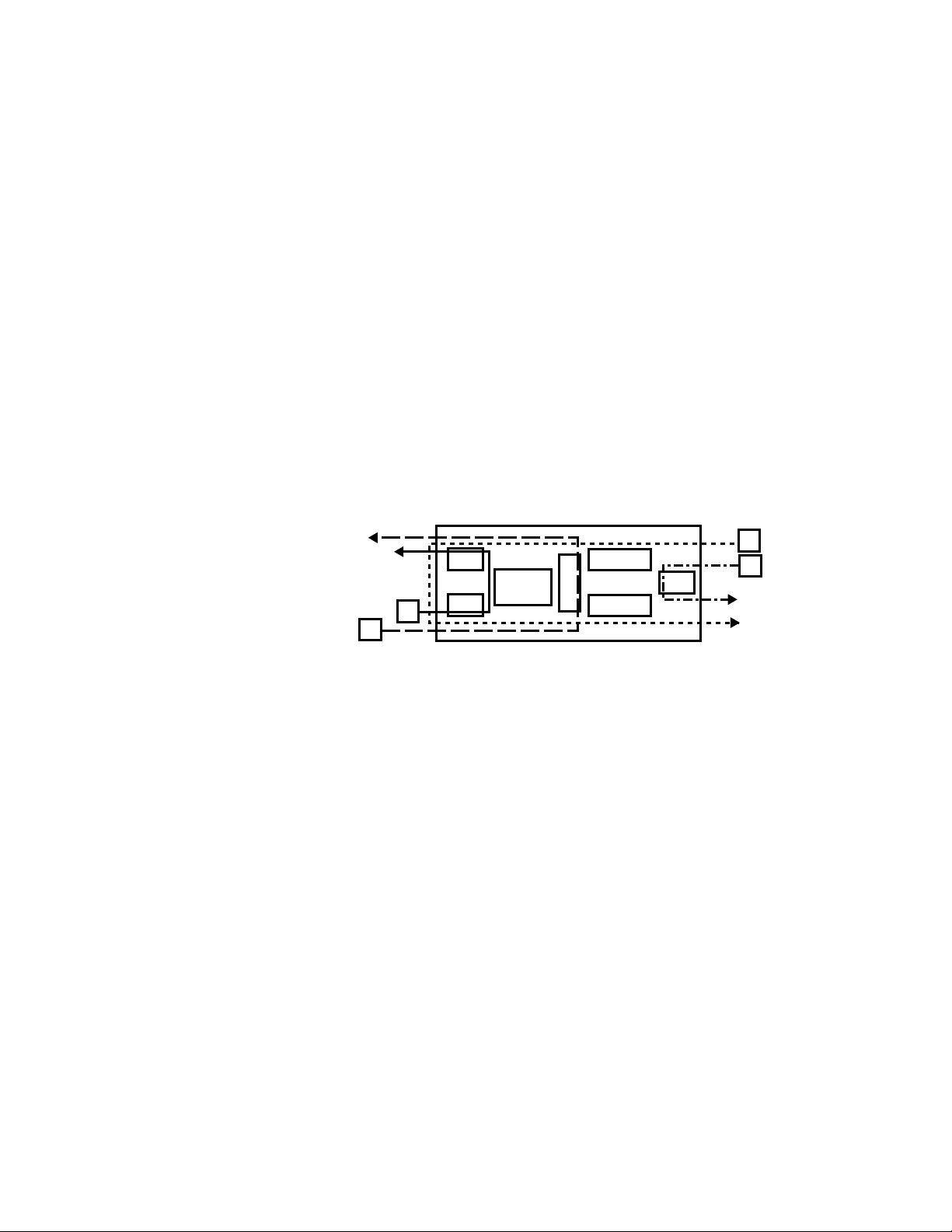
1.1 Internal Functional Blocks
See the Figure 1 block diagram.
1.2 HDMP-3001 Features List
• Full Duplex Fast Ethernet
(100 Mb/s) over SDH/SONET
(OC-3c/STM-1).
• Handles the source and sink of
SONET/SDH section, line, and
path layers, with E1, E2, F1
and D1-D12 overhead interfaces in both transmit and
receive directions.
• Implements the processing of
STS-3c/STM-1 data streams
with full duplex mapping of
LAPS or GFP frames into
SONET/SDH payloads.
• Self-synchronous scrambler/
descrambler implementing
(X43 +1) polynomial for LAPS/
GFP frames.
• Link-level scrambling function
to improve operational
robustness.
• Monitors link status when
mapping MAC frame into
SONET/SDH SPE. Statistics of invalid frames are also
provided.
• Device control, configuration,
and status monitoring by
either an 8-bit external
microprocessor interface or an
MII management interface.
• Compliant with SONET/ SDH
specifications ANSI T1.105,
Bellcore GR-253-CORE and
ITU G.707.
• Provides IEEE 1149.1 JTAG
test port.
• Supports internal loopback
paths for diagnostics.
• Packaged in a 160 pin PQFP.
• Typical power dissipation
250 mW.
8 BITS AT
19.44 MHz TO
TRANSCEIVER
PARALLEL
INTERFACE
TO
LINE
8 BITS AT
19.44 MHz FROM
TRANSCEIVER
Figure 1. Functional Block Diagram
5
8-BIT GENERIC
E1, E2, F1 AND DCC
TOH OVERHEAD
INSERT
TX FRAMER
TOH MONITOR POH MONITOR
RX FRAMER
TOH OVERHEAD
EXTRACT
E1, E2, F1 AND DCC
MICROPROCESSOR BUS
MICROPROCESSOR
SPE/VC
GENERATOR
POINTER
PROCESSOR
INTERFACE
X43 + 1
SCRAMBLER
X43 + 1
DESCRAMBLER
ETHERNET
MANAGEMENT BUS
MDIO INTERFACE EEPROM INTERFACE
LAPS/GFP
FRAME
PROCESSOR
PERFORMANCE
MONITOR
LAPS/GFP
FRAME
PROCESSOR
GPIO REGISTER
16 GENERAL
PURPOSE PINS
STANDARD 2-WIRE
EEPROM BUS
TX FIFO
ETHERNET
INTERFACE
RX FIFO
JTAG TEST
ACCESS PORT
TEST DATA
4 BITS AT
25MHz
MII
TO
SYSTEM
4 BITS AT
25MHz
Page 6
• Implemented in 0.25 micron
AGILENT
FIBER OPTICS
SERDES
WITH CDR
AGILENT
HDMP-3001
SWITCH
FABRIC
MICROPROCESSOR
ETHERNET
PHYs
MDIO BUS
OC-3c PORT ETHERNET PORTS
PORT ON ETHERNET SWITCH
LINE CARD OF SONET ADM
ETHERNET
PHY
AGILENT
HDMP-3001
ADM
EEPROM
SERDES
WITH CDR
AGILENT
FIBER OPTICS
DROP SIDE - 100 MBIT/S
FULL-DUPLEX ETHERNET
OC-48/12
SONET RING
MICROPROCESSOR
STAND ALONE DSU/CSU
ETHERNET
PHY
AGILENT
HDMP-3001
SONET SERDES
WITH CDR
AGILENT
FIBER OPTICS
100 MBIT/S
FULL-DUPLEX ETHERNET
OC-3c
CMOS with 1.8 V core, 3.3 V I/O
power and LVCMOS
compatible I/Os.
• Provides a 16-bit general purpose I/O (GPIO) register.
• Device power-up initialization
optionally through 2-wire
EEPROM interface.
• Configurable by hardware to
be connected to either a PHY
or a MAC from the system
connectivity viewpoint.
1.3 Applications
• Multi-Service Ethernet
Switches.
• Enhanced Services SONET/
SDH Add/Drop Multiplexers
(ADMs).
• DSU/CSUs.
1.4 Benefits
• Allows LANs to be interconnected over leased OC-3c
lines, thereby extending a LAN
to multiple sites.
• Ethernet switches in each LAN
can be connected together directly which reduces cost and
complexity.
• Enables Transparent LAN
Services which, unlike POS
solutions, do not require
WAN access routers.
1.5 Interfaces
• System interface is a 25 MHz
IEEE 802.3 full-duplex, 100
Mb/s Ethernet MII port that
connects to either a PHY or a
MAC.
• Line side SERDES interface is
8-bit parallel data operating at
19.44 MHz. SONET/SDH
framer is compliant to
specifications ANSI T1.105 and
ITU G.707.
• Serial data channels for add
and drop of SONET overhead
bytes E1, E2, F1 and DCC.
• 8-bit microprocessor
interface allows direct
connection to the Motorola
MPC860.
• IEEE 802.3 MDIO management
interface.
• Standard 2-wire EEPROM
interface for optional boot-up
configuration.
• Provides 16-bit General
Purpose I/O (GPIO) register.
• Provides standard five-pin
IEEE 1149.1 JTAG test port.
1.6 Data Processing
• Complies to the GFP (Generic
Framing Procedure) draft
specification, revision 2, of
ANSI T1X1.5 and implements
both the null and linear header
options.
• Complies to the LAPS (Link
Access Procedure – SDH)
specification X.86 of ITU.
• Optional self-synchronous
X43 +1 scrambling of the
payload.
Figure 2. HDMP-3001 Applications
6
Page 7
2. Pinout
2.1 Pin Assignments
DGND
RX_SDCC_CLK
RX_FRAME_SFP
DVDD
RX_LDCC_DATA
RX_LDCC_CLK
RX_SDCC_DATA
GND
DGND
RX_OOF_OUT
RX_LAIS_OUT
RX_8K_CLK
RX_LOS
NO CONNECT
RX_LOF_OUT
TX_DATA[0]
TX_DATA[1]
TX_DATA[2]
VDD
GND
DGND
DVDD
TX_DATA[3]
TX_DATA[4]
TX_DATA[5]
TX_DATA[6]
TX_DATA[7]
VDD
DGND
TX_SONETCLK
TX_8K_CLK
TX_E1E2F1_CLK
TX_E2_DATA
TX_E1_DATA
TX_F1_DATA
VDD
TX_FRAME_SFP
TX_LDCC_DATA
TX_LDCC_CLK
GND
GND
VDD
NO CONNECT
TRSTB
TMS
TDO
TCK
TDI
GPIO[0]
DGND
DGND
GPIO[1]
GPIO[2]
GPIO[3]
GPIO[4]
GPIO[5]
GPIO[6]
GPIO[7]
DVDD
DGND
GND
VDD
RX_FRAME_IN
RX_SONETCLK
RX_DATA[0]
RX_DATA[1]
RX_DATA[2]
RX_DATA[3]
RX_DATA[4]
BUSMODE1
GND
RX_DATA[5]
RX_DATA[6]
RX_DATA[7]
RX_E1E2F1_CLK
RX_F1_DATA
RX_E2_DATA
RX_E1_DATA
DVDD
DGND
DGND
155
5
10
15
20
25
30
35
45
150
50
145
55
140
60
135
65
130
70
125
115
110
105
100
95
90
85
75
DVDD
TX_SDCC_CLK
TX_SDCC_DATA
LOC_RX
LOC_TX
MDC
MDIO
P_TX_ER_M_RX_ER
GND
DGND
P_TX_EN_M_RX_DV
P_TXD_M_RXD[0]
P_TXD_M_RXD[1]
P_TXD_M_RXD[2]
P_TXD_M_RXD[3]
P_TX_CLK_M_RX_CLK
P_RX_ER_M_TX_ER
VDD
GND
DGND
DVDD
P_RX_DV_M_TX_EN
P_RXD_M_TXD[0]
P_RXD_M_TXD[1]
P_RXD_M_TXD[2]
P_RXD_M_TXD[3]
P_RX_CLK_M_TX_CLK
SCL
VDD
DGND
SDA
SYS_25M_CLK
BUSMODE0
INT
RSTB
CSB
APS_INTB
VDD
GND
VDD
GND
GPIO[9]
GPIO[8]
GPIO[11]
GPIO[10]
Figure 3. HDMP-3001 Pin Assignments
7
GPIO[13]
GPIO[12]
DGND
GPIO[14]
VDD
RDYB
GPIO[15]
WRB
RDB
ADDR[1]
ADDR[0]
DVDD
ADDR[2]
GND
CPU_CLK
VDD
ADDR[4]
ADDR[3]
ADDR[6]
ADDR[5]
ADDR[8]
ADDR[7]
D[0]
DGND
GND
D[1]
D[2]
D[3]
D[4]
D[5]
D[6]
D[7]
DVDD
DGND
Page 8

2.2 Pin Descriptions
Table 1. Line Side Interface Pins Description
Signal name Pin # Type(I/O) Signal description
RX_DATA[0] 25 I RECEIVE DATA: Byte-wide STS-3c data input stream.
RX_DATA[1] 26 RX_DATA [7] is the MSB, and RX_DATA [0] the LSB.
RX_DATA[2] 27 Data is sampled on the rising edge of RX_SONETCLK.
RX_DATA[3] 28
RX_DATA[4] 29
RX_DATA[5] 32
RX_DATA[6] 33
RX_DATA[7] 34
RX_FRAME_IN 23 I RECEIVE FRAME INDICATOR: Frame position indication signal is
active high and indicates the SONET frame position on the RX_
DATA [7:0] bus. Sampled on the rising edge of RX_SONETCLK.
Only used when RX_FRAME_INH is set, otherwise tie this pin low.
RX_LAIS_OUT 153 O RECEIVE LINE ALARM INDICATION SIGNAL OUTPUT:
Receive line alarm indication signal will be set high if a binary
“111” pattern is received for the number of consecutive frames
programmed into the K2_CONSEC register. RX_LAIS_OUT will
be cleared if a binary “111” pattern is not received for the
number of consecutive frames programmed into the
K2_CONSEC register.
RX_LOF_OUT 149 O RECEIVE LOSS OF FRAME OUTPUT:
RX_LOF_OUT is set high when there is a loss of frame indication.
If RX_OOF_OUT is active continuously for 24 consecutive frames
(3 ms), the RX_LOF bit is set high. Once RX_LOF is set, it remains
high until RX_OOF_OUT is inactive continuously for 3 ms.
RX_LOS 147 I RECEIVE LOSS OF SIGNAL: RX_LOS should be used to indicate
to the framer that there is no signal present from the optical
receiver. The signal’s default is active high, but can be set to
active low by programming RX_LOS_LEVEL = 1.
RX_OOF_OUT 152 O RECEIVE OUT OF FRAME OUTPUT: RX_OOF_OUT is set high when
there is an out of frame indication. An out of frame condition occurs
when five consecutive erroneous framing patterns specified
in the A1 or A2 bytes have been received.
RX_SONETCLK 24 I RECEIVE SONET CLOCK: RX_SONETCLK is the receive
input clock from the line side, and provides timing for the
receive data bus and frame position indication inputs.
This clock should be 19.44 MHz ± 20 ppm.
TX_DATA[0] 145 O TRANSMIT DATA: Byte-wide STS-3c data output stream.
TX_DATA[1] 144 TX_DATA [7] is the MSB, TX_DATA [0] is the LSB. Data is
TX_DATA[2] 143 updated on the rising edge of TX_SONETCLK.
TX_DATA[3] 138
TX_DATA[4] 137
TX_DATA[5] 136
TX_DATA[6] 135
TX_DATA[7] 134
(continues)
8
Page 9

Signal name Pin # Type(I/O) Signal description
TX_FRAME_SFP 125 O TRANSMIT FRAME POSITION OUTPUT INDICATOR: Frame position
indication signal is active high and indicates the SONET frame
position on the TX_DATA [7:0] bus. Updated on the rising edge of
TX_SONETCLK. This signal is also used for the outer board to start
sending the first bit (MSB) of the serial data E1, E2, F1, SDCC,
and LDCC.
TX_SONETCLK 133 I TRANSMIT SONET CLOCK: TX_SONETCLK is the transmit output
clock to the line side, and provides timing for the transmit data
bus and frame position indication outputs. This clock should be
19.44 MHz ± 20 ppm.
LOC_TX 115 O Loss of SONET_TX clock.
LOC_RX 116 O Loss of SONET_RX clock.
Table 2. MII Interface Pins Description
Signal name Pin # Type(I/O) Signal description
SYS_25M_CLK 88 I Drives the two MII clocks in PHY mode, TX_CLK and
RX_CLK. It is also used to monitor the TX_SONETCLK
and RX_SONETCLK.
The requirement for this clock is 25 MHz ±100 ppm.
P_TX_CLK_M_RX_CLK 104 I/O (Int. PU) PHY mode: transmit clock output. Derived from
SYS_25M_CLK.
MAC mode: receive clock input. Nominally 25 MHz.
P_TXD_M_RXD[0] 108 I PHY mode: transmit data nibble.
P_TXD_M_RXD[1] 107 MAC mode: receive data nibble.
P_TXD_M_RXD[2] 106
P_TXD_M_RXD[3] 105
P_TX_EN_M_RX_DV 109 I PHY mode: transmit data enable.
MAC mode: receive data valid.
P_RX_CLK_M_TX_CLK 93 I/O (Int. PU) PHY mode: receive clock output. Derived from
SYS_25M_CLK.
MAC mode: transmit clock input. Nominally 25 MHz.
P_RXD_M_TXD[0] 97 O (T/S) PHY mode: receive data nibble.
P_RXD_M_TXD[1] 96 MAC mode: transmit data nibble.
P_RXD_M_TXD[2] 95
P_RXD_M_TXD[3] 94
P_RX_DV_M_TX_EN 98 O (T/S) PHY mode: receive data valid.
MAC mode: transmit data enable.
P_RX_ER_M_TX_ER 103 O (T/S) PHY mode: receive error.
MAC mode: transmit error.
P_TX_ER_M_RX_ER 112 I PHY mode: transmit error.
MAC mode: receive error.
9
(continues)
Page 10

Signal name Pin # Type(I/O) Signal description
MDIO 113 I/O MII management input/output serial data. When this interface
is unused, connect this pin high. If HDMP-3001 is attached
to a MAC via the mechanical interface specified in IEEE 802.3,
clause 22.6, an external pull-up of 1.5 kohm ± 5% is required.
MDC 114 I MII management clock, up to 2.5 MHz. When this interface is
unused, connect this pin high.
Table 3. Transport Overhead Pins Description
Signal name Pin # Type(I/O) Signal description
RX_E1_DATA 38 O RECEIVED E1 DATA: Local orderwire channel data byte
(E1) received from the line side.
RX_E2_DATA 37 O RECEIVED E2 DATA: Express orderwire channel data byte
(E2) received from the line side.
RX_F1_DATA 36 O RECEIVED F1 DATA: Maintenance channel data byte (F1)
received from the line side.
RX_E1E2F1_CLK 35 O RECEIVED E1/E2/F1 DATA REFERENCE CLOCK: A
64 kHz clock reference output for E1/E2/F1 data. The MSB of
the E1/E2/F1 bytes appears in the first 64 kHz clock cycle
after a rising edge of RX_FRAME_SFP.
RX_FRAME_SFP 158 O RECEIVE FRAMER START-OF-FRAME INDICATION: This signal is
nominally 8 kHz and is high during the first row of overhead
of the received frame. The RX_FRAME_SFP signal is also used
for byte alignment of the received E1/E2/F1 data outputs. This
is a SFP (Start-of-Frame-Pulse) indicating the SONET frame
position on the RX_DATA [7:0] bus.
RX_LDCC_DATA 154 O RECEIVED LINE DCC DATA: Drop output for received
Line Data Communications Channel (DCC).
RX_LDCC_CLK 155 O RECEIVED LINE DCC REFERENCE CLOCK : A gapped 576 kHz clock
reference for Line DCC data. The RX_LDCC_DATA outputs are
updated on the falling edge of RX_LDCC_CLK.
RX_SDCC_DATA 156 O RECEIVED SECTION DCC DATA: Drop output for received Section
Data Communications Channel (DCC).
RX_8K_CLK 146 O 8kHz RECEIVE CLOCK: A general purpose 8kHz buffered clock
derived from RX_SONETCLK which may be used for external
clock reference purposes.
RX_SDCC_CLK 157 O RECEIVED SECTION DCC REFERENCE CLOCK : A gapped 192 kHz
clock reference for Section DCC data. The RX_SDCC_DATA outputs are updated on the falling edge of RX_SDCC_CLK.
(continues)
10
Page 11

Signal name Pin # Type(I/O) Signal description
TX_E1_DATA 126 I TRANSMIT E1 DATA: Local orderwire channel data byte
(E1) to be inserted by the HDMP-3001 into the outgoing
SONET data stream.
TX_E2_DATA 127 I TRANSMIT E2 DATA: Express orderwire channel data byte
(E2) to be inserted by the HDMP-3001 into the outgoing
SONET data stream.
TX_F1_DATA 128 I TRANSMIT F1 DATA: Maintenance channel data byte (F1)
to be inserted by the HDMP-3001 into the outgoing SONET
data stream.
TX_E1E2F1_CLK 129 O TRANSMIT E1/E2/F1 DATA REFERENCE CLOCK: A 64 kHz clock
reference output for E1/E2/F1 data to be inserted by the
HDMP-3001 into the outgoing SONET data stream.
TX_LDCC_DATA 123 I TRANSMIT LINE DCC DATA: Input for the Line Data
Communications Channel (DCC) to be inserted by the HDMP-3001
into the outgoing SONET data stream.
TX_LDCC_CLK 124 O TRANSMIT LINE DCC REFERENCE CLOCK: A 576 kHz clock
reference for Line DCC data to be inserted by the
HDMP-3001 into the outgoing SONET data stream. The
TX_LDCC_DATA inputs are sampled on the falling edge of
TX_LDCC_CLK.
TX_SDCC_DATA 117 I TRANSMIT SECTION DCC DATA: Input for the Section
Data Communications Channel (DCC) to be inserted into the
outgoing SONET data stream from the HDMP-3001.
TX_SDCC_CLK 118 O TRANSMIT SECTION DCC REFERENCE CLOCK:
A 192 kHz clock reference for Section DCC data to be inserted
by the HDMP-3001 into the outgoing SONET data stream. The
TX_SDCC_DATA inputs are sampled on the falling edge of
TX_LDCC_CLK.
TX_8K_CLK 132 O 8kHz TRANSMIT CLOCK: A general purpose 8kHz
buffered clock derived from TX_SONETCLK which may be
used for external clock reference purposes.
11
Page 12

Table 4. Microprocessor Interface Pins Description
Signal name Pin # Type(I/O) Signal description
ADDR[0] 56 I ADDRESS BUS: Allows host microprocessor to perform
ADDR[1] 57 register selection within the HDMP-3001.
ADDR[2] 58
ADDR[3] 63
ADDR[4] 64
ADDR[5] 65
ADDR[6] 66
ADDR[7] 67
ADDR[8] 68
APS_INTB 83 O (O/D) APS INTERRUPT: Active-low output triggered by an APS
event. APS_INTB is an open-drain output which is in a high
impedance state when inactive.
When used, this pin needs an external pull-up.
BUSMODE0 87 I/O BUS INTERFACE MODE:
BUSMODE1 30
BUSMODE1, BUSMODE0 = 00 -> Motorola MPC860 mode
BUSMODE1, BUSMODE0 = 01 -> Reserved
BUSMODE1, BUSMODE0 = 10 -> Reserved
BUSMODE1, BUSMODE0 = 11 -> Reserved
Both pins are latched at reset and are also used as test outputs in
test mode. In normal applications, tie these pins low.
CPU_CLK 60 I CPU CLOCK: Used in Motorola MPC860 mode.
CSB 84 I CHIP SELECT: Active-low chip select.
D[0] 69 I/O I/O DATA BUS: Allows transfer of data between host
D[1] 72 microprocessor and the HDMP-3001.
D[2] 73 Refer to microprocessor application notes on the usage of
D[3] 74 board level pull-ups.
D[4] 75
D[5] 76
D[6] 77
D[7] 78
12
(continues)
Page 13

Signal name Pin # Type(I/O) Signal description
INT 86 O (T/S) INTERRUPT: Configurable interrupt output. Refer to
Table 18 for a detailed description of how INT is configured.
In open-drain configurations, an external pull-up is required.
In open-source configurations, an external pull-down is
required.
To prevent undesired interrupts before configuration is
complete, microprocessors with an active-high interrupt pin
should have a pull-down and those with an active-low interrupt
pin, a pull-up.
RDB 55 I READ ENABLE: Active low.
RDYB 53 I/O READY: RDYB is an active-low output to acknowledge the
end of data transfer. This pin is briefly driven to its inactive state
before being tristated.
Refer to microprocessor application notes for board pull-up
requirements.
RSTB 85 I RESET: Active low input to reset the HDMP-3001.
WRB 54 I WRITE ENABLE: Active low.
Table 5. JTAG Interface Pins Description
Signal name Pin # Type(I/O) Signal description
TCK 7 I TEST CLOCK: JTAG input clock used to sample data on the
TDI and TDO pins. Should be tied high when the JTAG interface
is not in use.
TDI 8 I (Int PU) TEST DATA IN: Input pin for serial data stream to be sent to
HDMP-3001. TDI is sampled on the rising edge of TCK.
TDO 6 O TEST DATA OUT: Output pin for serial data stream sent
from the HDMP-3001. TDO is sampled on the falling edge of` TCK.
TMS 5 I (Int. PU) TEST MODE SELECT: Controls the operating mode of the
JTAG interface. TMS is sampled on the rising edge of TCK.
TRSTB 4 I (Int. PU) TEST PORT RESET: Active low input used to reset the
JTAG interface.
13
Page 14

Table 6. Two-Wire EEPROM Interface Pins Description
Signal name Pin # Type(I/O) Signal description
SCL 92 I/O EEPROM bus clock. If no EEPROM is present, connect this pin
to ground.
Refer to EEPROM application notes for board pull-up requirements.
SDA 89 I/O EEPROM bus data. If no EEPROM is present, connect this pin
to ground.
Refer to EEPROM app notes for board pull-up requirements.
Table 7. Miscellaneous Pins Description
Signal name Pin # Type(I/O) Signal description
GPIO[0] 9 I/O (int. PU) GENERAL PURPOSE I/O: The GPIO register allows the
GPIO[1] 12 user to define each grouping (GPIO [0, 1], GPIO [2, 3], GPIO [4, 5],
GPIO[2] 13 GPIO[6, 7], GPIO [8, 9], GPIO [10, 11], GPIO [12, 13],
GPIO[3] 14 GPIO [14, 15] ) as either input or output bits. These bits can
GPIO[4] 15 be used for functions such as LED control or user-defined
GPIO[5] 16 input control.
GPIO[6] 17
GPIO[7] 18
GPIO[8] 43
GPIO[9] 44
GPIO[10] 45
GPIO[11] 46
GPIO[12] 47
GPIO[13] 48
GPIO[14] 49
GPIO[15] 52
NO CONNECT 3, 148 These pins should be left unconnected.
GND 1, 21, 31, Logic GROUND: These pins should be connected to the logic
41,61, 71, ground plane.
81, 101,
111, 121,
141, 151
(continues)
14
Page 15

Signal name Pin # Type(I/O) Signal description
DGND 10, 11, 20, Driver GROUND: These pins should be connected to the I/O
40, 50, ground plane.
70, 80,
90, 100,
110, 120,
130, 140,
150, 160
VDD 2, 22, Logic POWER: These pins should be connected to the 1.8 V
42, 51, power supply for logic.
62, 82,
91, 102,
122, 131,
142
DVDD 19, 39, Driver POWER: These pins should be connected to the 3.3 V
59, 79, power supply for I/O.
99, 119,
139, 159
Note:
I = Input, O = output, T/S = Tristateable output, O/D = Open-drain output, and Int. PU = Internal pull-up.
15
Note: All unused inputs must be tied off to their inactive states. No input pins
should be left floating.
Page 16

2.3 I/O Buffer Types
This section lists the types of some particular I/Os used in the HDMP-3001 chip.
Table 8. Buffer types
Buffer Type I/O Name Comment
O/D APS_INTB Need external P/U
Output
TS P_RXD_M_TXD[0] Controlled by the “Isolate MII” register bit
Output P_RXD_M_TXD[1]
P_RXD_M_TXD[2]
P_RXD_M_TXD[3]
P_RX_DV_M_TX_EN
P_RX_ER_M_TX_ER
INT See INT Pin Configuration Section
RDYB Uses a T/S output buffer and logically drives high before output buffer is
released or tristated
Input TMS, TRSTB, TDI
w/
Internal P/U
Bidirectional
P_TX_CLK_M_RX_CLK
w/
Internal P/U
for input
mode
P_RX_CLK_M_TX_CLK
SDA P/U can be disabled if there is an external P/U
SCL
GPIO [15:0]
Note:
All of the internal P/Us are normally enabled, and they can be disabled through the JTAG port, with the exception of SCL and SDA.
The pullups on these two pins can be disabled using controls from register 0x003 bits [5:4].
16
Page 17

3. Functional Description
3.1 Introduction
The HDMP-3001 performs fullduplex mapping of Ethernet
frames into a SONET STS-3c /
SDH STM-1 payload using the
LAPS or GFP protocol. All
SONET/SDH framing functions
are included. A TOH
interface provides direct add/drop
capability for E1, E2, F1, and both
Section and Line DCC channels.
SONET or SDH mode is selected
during initial configuration.
By default, the HDMP-3001 operates in LAPS mode. LAPS is a
HDLC-compatible protocol. The
LAPS transmit processing includes packet framing,
inter-frame fill, payload scrambling (X43 +1), transparency
processing (byte stuffing) and 32bit CRC generation. The receive
LAPS processing provides for the
extraction of LAPS frames, transparency removal, descrambling,
header and FCS checking.
The HDMP-3001 can also be configured to operate in GFP mode.
The GFP transmit processing includes the insertion of framed
packet framing, idle frame insertion, payload scrambling (X43 +1)
and 32-bit CRC generation. The
receive GFP processing provides
for the extraction of GFP frames,
descrambling, header and FCS
error checking.
A robust set of performance
counters and status/control registers for performance monitoring
via the external microprocessor
or MDIO is provided.
The SONET/SDH line side consists of an 8-bit parallel interface
which operates at 19.44 MHz.The
device is typically connected to a
parallel-to-serial converter, which
is in turn connected to an optical
transceiver for interfacing to a
fiber. The Ethernet interface is a
standard MII interface which operates at 25 MHz (4-bit). Only 100
Mb/s full-duplex operation is supported, i.e. collisions are not
supported. This device can be
controlled through either a microprocessor port or a two-wire
MDIO (MII Management)
port. The complete register map
can be accessed from both these
ports. Additionally, the initial configuration can be automatically
downloaded from an EEPROM
which is useful in designs without
on-board intelligence.
3.2 Interface Descriptions
3.2.1 Microprocessor Interface
The interface consists of eight
data bits, nine address bits, three
control signals and one acknowledge signal. Through this
interface the HDMP-3001 internal
register map can be accessed.
Only one of the microprocessor,
MII Management or EEPROM
ports can be active at any one
time. Hence, in the rare cases
where more than one port is used,
care has to be taken not to have
more than one port active simultaneously.
3.2.2 MII Management Interface
The MII Management interface is
a standard port for Ethernet PHYs
and is defined in the IEEE 802.3
specification. It is a two wire interface that allows access to
thirty-two sixteen-bit data registers. These are defined in the MII
Management memory map. Sixteen of the data registers are
defined by the IEEE specification
and sixteen are left for vendor
specific purposes. Two of the vendor specific registers in the
HDMP-3001 are used to enable
access to the internal chip registers through indirect addressing.
One of the vendor specific registers is used to shadow the
frequently polled master alarm
register.
3.2.3 EEPROM Interface
This port operates in master mode
only, i.e. the HDMP-3001 cannot
be accessed through this port.
One use of this port is to configure the chip in stand-alone
applications. Another use is to
assign unique PHY addresses to
cascaded HDMP-3001 ICs when
they are controlled through the
MDIO port.
If enabled, this port is automatically activated after reset to load
the HDMP-3001 configuration
from an EEPROM. The complete
address space of the HDMP-3001,
511 to 0, is filled with the data
from EEPROM addresses 511 to 0.
EEPROMs like Philips’
PCF8594C-2, Fairchild’s
NM24C02U or Atmel’s AT24C04
are supported. The EEPROM device address should be set to zero.
The SCL clock rate is just under
100 kHz. It takes a little under 300
ms for the EEPROM to load, so
during this time the microprocessor and MII Management ports
must stay inactive.
3.2.4 MII Interface
This interface is a 100 Mb/s fullduplex Ethernet MII interface as
defined by IEEE 802.3. It operates
at 25 MHz. At power-up the MII
Isolate bit in the register map is
active, which sets all output pins
in this interface to high impedance
and ignores all MII inputs.
17
Page 18
3.2.5 SONET/SDH Interface
This interface is 8 bits wide and
runs at 19.44 MHz. The Serial
SONET/SDH overhead channels
are clocked in and out of the IC
through low-speed serial ports.
3.3 Initialization
3.3.2 Software Reset
Software resets are functionally
equivalent to hardware resets.
There are two identical software
resets, one in the microprocessor
register map and one in the MII
register map. Both resets are selfcleared in less than 10 µs.
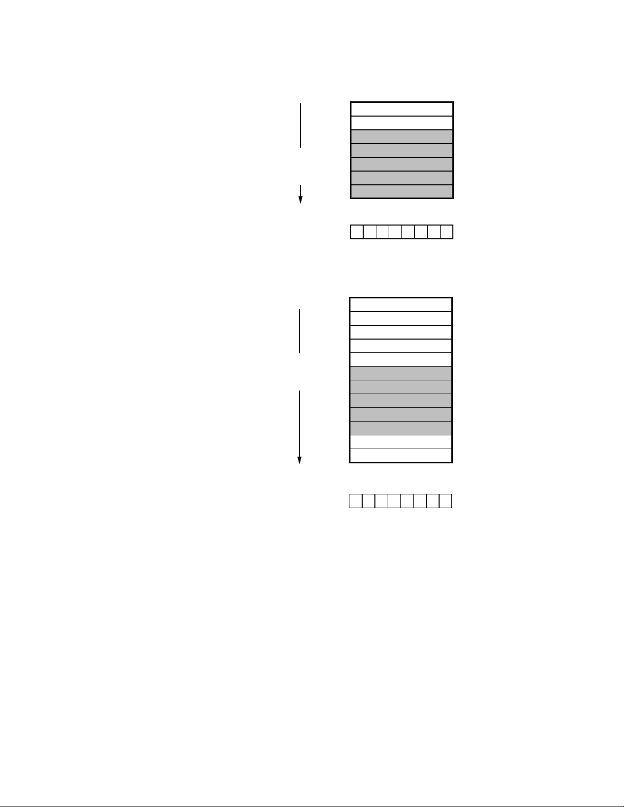
3.4 Bit Order
3.4.1 GFP Mode
The bit order for the MII nibbles
through the HDMP-3001 chip is
shown in Figure 4. The order in
which the FCS bits are transmitted is shown in Figure 5.
3.3.1 Hardware reset
The HDMP-3001 hardware reset,
RSTB, is asynchronous and must
be active for at least 200 SONET
clock cycles (>10 µs) with stable
power.
PINS
TX_DATA[7]
TX_DATA[6]
TX_DATA[5]
TX_DATA[4]
TX_DATA[3]
TX_DATA[2]
TX_DATA[1]
TX_DATA[0]
7
6
X
7
S
C
R
F = FIRST
L = LAST
F
7 6 5 4 3 2 1 0
[7] [0]
5
4
3
2
1
0
3.3.3 Software State Machine Reset
This reset should always be active
when the chip is configured. Only
when the configuration is completed should the state machine
reset be cleared to begin normal
operation.
X
4
3
S
C
R
C
R
C
G
E
N
F
7 6 5 4 3 2 1 0
F
7 6 5 4 3 2 1 0
L
L
7
6
M
5
G
F
P
I
I
4
3
I
2
/
1
F
0
L
F
0
1
2
3
LSN
MSN
L
PINS
4
5
6
7
TXD0
TXD1
TXD2
TXD3
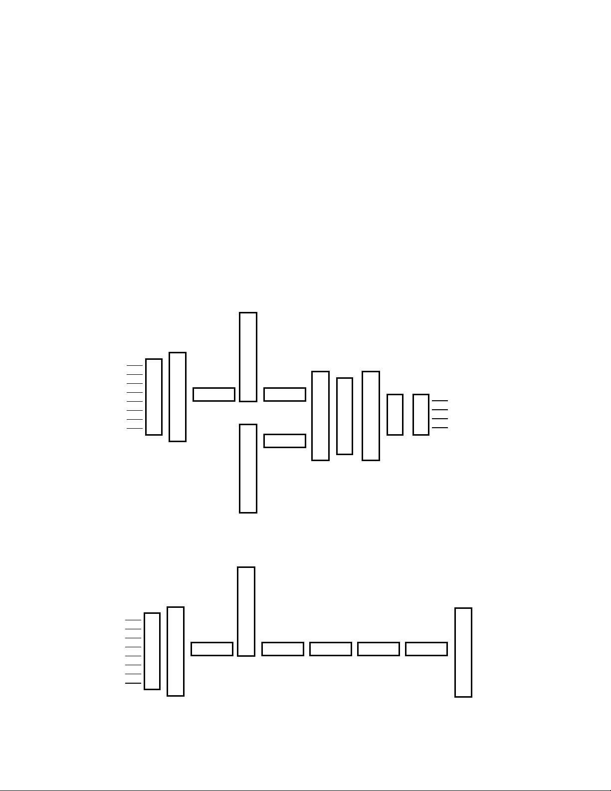
Figure 4. GFP Payload Bit Order
PINS
TX_DATA[7]
TX_DATA[6]
TX_DATA[5]
TX_DATA[4]
TX_DATA[3]
TX_DATA[2]
TX_DATA[1]
TX_DATA[0]
7
6
5
4
3
2
1
0
Figure 5. GFP FCS Bit Order
18
X
7
S
C
R
F
7 6 5 4 3 2 1 0
[7] [0]
X
4
3
S
C
R
L
F
7 6 5 4 3 2 1 0
31
X
24
X
7 6 5 4 3 2 1 0
23
X
16
X
7 6 5 4 3 2 1 0
15
X
8
X
7 6 5 4 3 2 1 0
7
X
C
L
R
C
0
G
X
E
N
Page 19
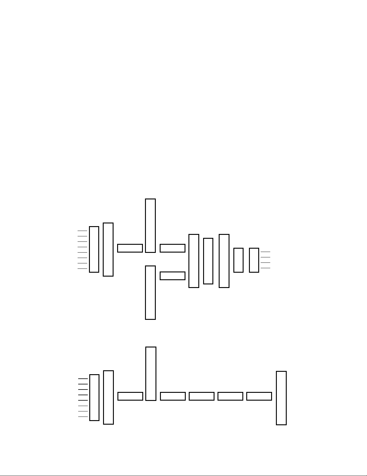
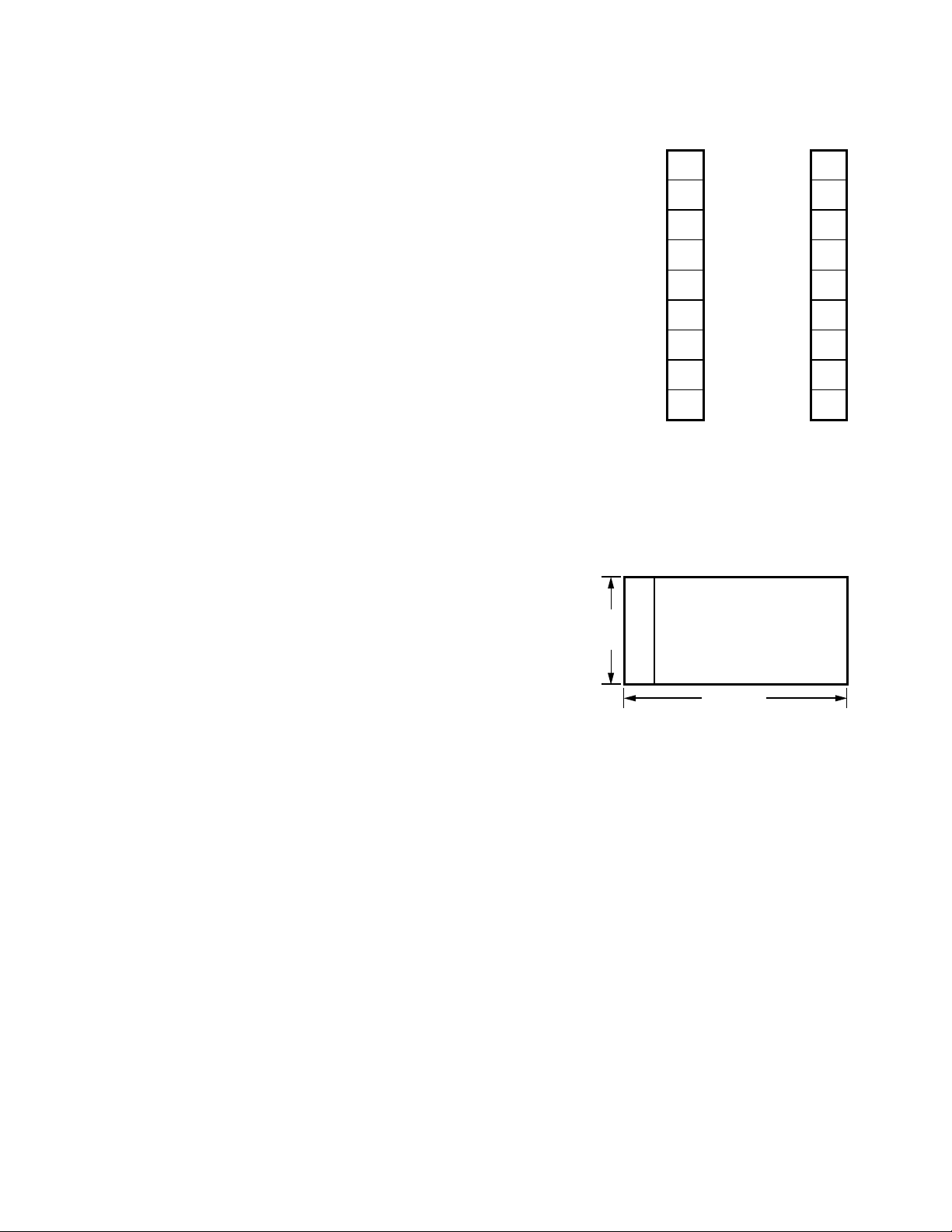
3.4.2 LAPS Mode
In LAPS mode the FCS is calculated LSB first and the FCS sum is
transmitted in reversed bit order
within each byte. See Figure 6 and
Figure 7.
3.5 Performance Monitoring
For performance monitoring purposes, the HDMP-3001 contains a
number of delta bits, event bits
and error counters.
Delta bits are set by the HDMP3001 when a monitored parameter
changes state. The delta bit then
stays high until the controller
PINS
TX_DATA[7]
TX_DATA[6]
TX_DATA[5]
TX_DATA[4]
TX_DATA[3]
TX_DATA[2]
TX_DATA[1]
TX_DATA[0]
7
6
X
7
S
C
R
F = FIRST
L = LAST
F
7 6 5 4 3 2 1 0
[7] [0]
5
4
3
2
1
0
clears the bit. If a clear occurs simultaneously with a parameter
state change, the delta bit remains
set. Delta bits are indicated by a
_D suffix.
When LATCH_CNT in register
0x001 is written from a 0 to a 1, it
produces a pulse on an internal
signal, LATCH_EVENT.
All the internal performance
monitoring counter blocks are
comprised of a running error
counter and a holding register
that presents stable results to the
controller. The counts in all of the
X
4
3
S
C
R
C
R
C
G
E
N
F
7 6 5 4 3 2 1 0
F
0 1 2 3 4 5 6 7
L
L
7
6
M
5
L
4
A
P
3
S
2
/
1
F
0
L
running counters are latched into
the hold registers and the running
counters are cleared when a pulse
occurs on LATCH_EVENT.
To prevent missing a count that
occurs when latching occurs, a
counter is set to one, rather than
zero, if the clear signal is simultaneous with an increment. After
being latched, the results are held
to be read by the microprocessor.
The running counters will stop at
their maximum value rather than
roll over to zero.
F
L
PINS
TXD0
4
0
I
1
I
2
I
3
LSN
MSN
TXD1
5
TXD2
6
TXD3
7
Figure 6. LAPS Payload Bit Order
PINS
TX_DATA[7]
TX_DATA[6]
TX_DATA[5]
TX_DATA[4]
TX_DATA[3]
TX_DATA[2]
TX_DATA[1]
TX_DATA[0]
7
6
5
4
3
2
1
0
Figure 7. LAPS FCS Bit Order
19
X
F
7
S
[7] [0]
C
R
7 6 5 4 3 2 1 0
X
4
3
S
C
R
L
F
7 6 5 4 3 2 1 0
24
X
31
X
7 6 5 4 3 2 1 0
16
X
23
X
7 6 5 4 3 2 1 0
8
X
15
X
7 6 5 4 3 2 1 0
0
X
C
L
R
C
7
G
X
E
N
Page 20
Summary delta event bits provide
a consolidated view of the various
individual delta event bits,
grouped either by function or
SONET tributary. Summary delta
events are therefore a function of
the other delta events bits in the
register maps. The summary bits
are read only, and will only be
cleared when all delta event bits
that contribute to them are
cleared.
The summary bits are O/R'd together to form the HDMP-3001
interrupt outputs, INTB and
APS_INTB. The contribution of
any of these bits to the summary
interrupts can be deleted by setting the corresponding mask bit.
3.6 Test
3.6.1 Loopbacks
Several loopbacks are provided
for test purposes, as shown in
Figure 8:
• Loopback 1:
SONET_R_TO_R_LOOPL,
requires STS-3c/STM-1 mode
with TX_SONETCLK =
RX_SONETCLK.
• Loopback 2:
SONET_R_TO_T_LOOP,
requires STS-3c/STM-1 mode
with TX_SONETCLK =
RX_SONETCLK.
• Loopback 3: Loopback done
on the board level.
• Loopback 4:
MII_T_TO_R_LOOP, only
supported in PHY mode, i.e.
when the HDMP-3001 drives
the MII clocks.
The loopback modes are selected
by programming register bits in
the register map. For details
please refer to the description of
register 0x001.
In SONET loopback mode
SONET_R_TO_T_LOOPL, the
data received on the RX_DATA
pins is routed straight to the
TX_DATA pins. The data is not
processed by the chip. In SONET
loopback mode
SONET_R_TO_T_LOOP, the data
received on the RX_DATA pins is
processed by the line side receive
circuitry. After the framer the
1
2
Figure 8. Loopbacks
TX TX_LAPS
OVERHEAD
RX
F
I
F
O
data is looped back to the line
side transmit circuitry, from
where it is sent out on the
TX_DATA pins.
The Ethernet loopback mode can
be enabled by setting register bit
MII_LOOPBACK_MODE. In
loopback mode, the MII RX interface and MII TX interface are
used together to route the MAC
frames from the MAC device back
to the MAC device. That is, the
MAC frames under test are received from the MAC device
through the MII TX interface.
Then, the MAC frames are not
processed and are sent directly to
the MII RX interface.
THIRD LOOPBACK
3
OUTSIDE CHIP
4
MII
RX_LAPS
20
Page 21

3.6.2 JTAG
The HDMP-3001 supports the
IEEE 1149.1 Boundary Scan standard. The Test Access Port
consists of 5 pins as defined in
Table 10. Signals TDI, TMS and
TRSTSB are all pulled up to logic
one when not driven.
Table 9. JTAG pins
Signal Name Description
TDI Signal input to the TAP controller
TMS TAP controller state machine control
TCK TAP controller clock
The HDMP-3001 TAP supports the
mandatory EXTEST, SAMPLE/
PRELOAD, and BYPASS instructions along with the optional
CLAMP and HIGHZ instructions.
The instructions and their
opcodes are listed in Table 11.
The TAP generates a two-phase
non-overlapping clock to control
the boundary scan chain based
upon the input signal TCK. The
TAP controller is optimized to
work at 10 MHz.
3.7 Interrupts
The microprocessor interface can
be operated in either an interrupt
driven or a polled mode. In both
modes, the HDMP-3001 register
bit SUM_INT can be used to determine whether or not changes have
occurred in the state of monitoring registers.
3.7.1 Interrupt Driven Mode
In an interrupt driven mode, the
SUM_INT_MASK bit should be
cleared. This allows the INT output to become active. In addition,
the RX_APS_INT_MASK bits of
the receive side should be cleared
(to logic zero). This allows the
APS_INTB output to become active (logic zero). If an interrupt
occurs, the microprocessor can
first read the summary status registers to determine the class(es)
of interrupt source(s) that is active, and then read the specific
registers in that class(es) to determine the exact cause of the
interrupt.
TRSTB Asynchronous TAP reset
TDO Scan output from TAP
Table 10. JTAG instructions supported
Instruction Opcode Description
EXTEST 00 Board Level Interconnection Testing
SAMPLE/ PRELOAD 02 Snapshots of Normal Operation
BYPASS FF Normal Chip Operation
HIGHZ 08 Outputs in High Impedance State
CLAMP 04 Holds Values from Boundary-Scan
Chain to Outputs
3.7.2 Polled Mode
The SUM_INT_MASK and
RX_APS_INT_MASK bits should
be set to logic 1 to suppress all
hardware interrupts and operate
in a polled mode. In this mode,
the HDMP-3001 outputs INT and
APS_INTB are held in the inactive
(logic one) state.
Note that the SUM_INT_MASK
and RX_APS_INT_MASK bits do
not affect the state of the register
bits SUM_INT and RX_APS_INT.
These bits can be polled to determine if further register
interrogation is needed.
3.7.3 Interrupt Sources
The interrupt sources are divided
into four groups. Each group can
be masked and each interrupt
source within the group can be
individually masked.
TOH_D_SUM group indicates
that at least one of the delta signals below is unmasked and set.
RX_LOS_D, RX_OOF_D,
RX_LOF_D, RX_LAIS_D,
RX_LRDI_D, RX_K1_D,
K1_UNSTAB_D,
RX_K2_D, J0_OOF_D
PTR _D_SUM group indicates
that at least one of the delta signals below is unmasked and set.
RX_PAIS_D, RX_LOP_D
PATH_D_SUM group indicates
that at least one of the delta signals below is unmasked and set.
RX_PLM_D, RX_UNEQ_D,
RX_G1_D, RX_C2_D, J1 _AVL,
J1_OOF_D
21
Page 22
EOS_D_SUM group indicates
that at least one of the delta signals below is unmasked and set.
NEW_RX_MIN_ERR,
NEW_RX_MAX_ERR,
NEW_RX_OOS_ERR,
NEW_RX_FORM_DEST_ERR,
NEW_RX_FIFO_UR_ERR,
NEW_RX_FIFO_OF_ERR,
NEW_RX_FCS_HEC_ERR,
NEW_TX_FIFO_UR_ERR,
NEW_TX_FIFO_OF_ERR,
NEW_TX_ER_ERR,
NEW_TX_MII_ALIGN_ERR
3.7.4 APS_INTB
RX_APS_INT interrupt message
for APS (K1 and K2) indicates that
at least one of the RX_K1_D,
RX_K2_D, K1_UNSTAB_D is one
and the corresponding mask bits
and RX_APS_INT_MASK are zero.
3.8 Data Processing
The LAPS and GFP TX Processing
refers to the encapsulation of the
MAC (Media Access Control)
frames coming from the MII (Media Independent Interface, see
IEEE 802.3 specification) into the
LAPS/GFP frames, which are then
sent to the Line Side Interface
(SONET/SDH). Figure 9 shows an
Ethernet MAC frame, and Figure
10 a LAPS frame with a MAC payload.
3.8.1 LAPS Processing
The Transmit LAPS Processor
provides the insertion of packetbased information into the STS
SPE. It provides packet encapsulation, FCS field generation,
inter-packet fill and scrambling.
The Transmit LAPS Processor
performs the following functions:
• Encapsulates packets within
an LAPS frame. Each packet is
encapsulated with a start flag
(0x7E), a 32-bit FCS field,
Address, Control and SAPI
PREAMBLE
START OF FRAME DELIMITER
DESTINATION ADDRESS (DA)
OCTETS WITHIN
FRAME ARE
TRANSMITTED FROM
TOP TO BOTTOM
MSB
Figure 9. An Ethernet MAC frame
MSB
MSB
MSB
MSB
OCTETS WITHIN
FRAME ARE
TRANSMITTED FROM
TOP TO BOTTOM
Figure 10. The format of a LAPS frame with a MAC payload
MSB
MSB
MSB
fields, and an end of field flag
(0x7E). All fields except the
start flag can be disabled
through configuration.
• Optional self-synchronous
transmit payload scrambler
(X43 +1 polynomial).
• Transparency processing
(octet stuffing for Flags &
Control Escape). Byte stuffing
occurs between start and end
of field flags. Stuffing replaces
SOURCE ADDRESS (SA)
LENGTH/TYPE
MAC CLIENT DATA
FCS
BIT 7 BIT 0
FLAG (0x7E)
ADDRESS (0x04)
CONTROL (0x03)
SAPI MSB (0xFE)
SAPI LSB (0x01)
DESTINATION ADDRESS (DA)
SOURCE ADDRESS (SA)
LENGTH/TYPE
MAC CLIENT DATA
FCS OF MAC
FCS OF LAPS
FLAG (0x7E)
BIT 8 BIT 1
each byte within a frame that
matches the flag or control
code bytes with a two-byte
sequence.
• Provides the ability to insert
FCS errors for testing under
SW control.
• Provides for selectable
treatment of FIFO underflow.
A FIFO underflow condition
occurs when a TX FIFO empty
occurs prior to the end of a
7 OCTETS
1 OCTET
6 OCTETS
6 OCTETS
2 OCTETS
46 - 1500 OCTETS
4 OCTETS
LSB
1 OCTET
LSB
1 OCTET
LSB
1 OCTET
LSB
1 OCTET
LSB
1 OCTET
LSB
6 OCTETS
6 OCTETS
2 OCTETS
46 - 1500 OCTETS
4 OCTETS
4 OCTETS
LSB
LSB
MAC
FRAME
1 OCTET
22
Page 23

packet. When this occurs an
interrupt is generated. The
packet can be ended via
generation of an FCS error, via
an abort sequence, or via “fill”
bytes inserted in the gap,
depending upon a software
configurable escape code.
• Maintains performance
monitor counters.
3.8.1.1 FCS Polynomial for LAPS
Processing
The HDMP-3001 supports CRC-32
Frame Check Sequence (FCS)
generation and checking. The
polynomial used to generate and
check the FCS is
X32 + X26 + X23 + X22 + X16 + X
12
+ X11 + X10 + X8 + X7 + X5 + X4 +
X2 + X + 1.
The FCS field is calculated over
all bits of the Address, Control,
Payload, Information and Padding
fields, not including any octets
inserted for transparency. This
does not include the Flag Sequences nor the FCS field itself.
The CRC generator and checker
are initialized to all ones. Upon
completion of the FCS calculation
the FCS value is ones-complemented. It is this new value that is
inserted in the FCS field.
3.8.1.2 LAPS Scrambling
Scrambling is performed to protect the SONET/SDH line against
malicious users deliberately sending packets to cause long
run-lengths of ones or zeros or
replicating the SONET/SDH framing bytes. In the transmit
direction an X43 +1 scrambler
scrambles all SPE payload data.
In the receive direction, a self-synchronous X43 +1 descrambler
recovers the scrambled data.
3.8.2 GFP Processing
The Transmit GFP Processor provides the insertion of packetbased information into the STS
SPE. It provides packet encapsulation, FCS field generation,
inter-packet fill and scrambling.
The GFP Processor performs the
following functions:
• Counts the Ethernet frame
length.
• Calculates the payload length
field, (PLI).
• Performs XOR with values as
shown in Figure 11.
• Generates and sends cHEC
and XOR (Figure 11).
• Sends programmable TYPE
values.
• Generates and sends tHEC.
• Sends programmable DP, SP,
and SPARE.
• Generates and sends eHEC.
• Generates and sends optional
FCS.
3.8.2.1 FCS Polynomial for GFP
Processing
The HDMP-3001 supports CRC-32
Frame Check Sequence (FCS)
generation and checking. The
polynomial used to generate and
check the FCS is
X32 + X26 + X23 + X22 + X16 + X
12
+ X11 + X10 + X8 + X7 + X5 + X4 +
X2 + X + 1.
The FCS field is calculated over
the GFP payload, excluding all
headers. The CRC generator and
checker are initialized to all ones.
Upon completion of the FCS calculation the FCS value is
ones-complemented. It is this new
value that is inserted in the FCS
field.
3.8.2.2 HEC Polynomial for GFP
Processing
The following polynomial is used
for generating and checking the
HECs:
X16 + X12 + X5 + 1
An HEC is calculated over each
header. The initial value of the
CRC registers is zero and the HEC
is not inverted before being sent.
23
Page 24

NOTE: ‘+’ IN THE DIAGRAM BELOW IS AN EXCLUSIVE OR FUNCTION
MSB PLI '+' 0xB6 NUMBER OF BYTES IN THE GFP PAYLOAD
LSB PLI '+' 0xAB
MSB cHEC '+' 0x31
NON-SCRAMBLED
LSB cHEC '+' 0xE0
MSB TYPE PROGRAMMABLE
LSB TYPE PROGRAMMABLE
MSB tHEC
LSB tHEC
DP PROGRAMMABLE SP PROGRAMMABLE
SPARE
MSB eHEC
LSB eHEC
+ 1)
43
OCTET TRANSMISSION ORDER
SCRAMBLED (X
MSB FCS[31:24] 1) 32-BIT CRC POLYNOMIAL
FCS[23:16] 2) ON PRE-SCRAMBLED DATA
FCS[15:8] 3) COVERS THE GFP PAYLOAD DATA ONLY
LSB FCS[7:0]
BIT TRANSMISSION ORDER
Figure 11. The GFP frame
3.8.2.3 GFP Scrambling
Scrambling is performed to protect the SONET/SDH line against
malicious users deliberately sending packets to cause long
run-lengths of ones or zeros or
replicating the SONET/SDH framing bytes. In the transmit
direction an X43 +1 scrambler
scrambles all SPE payload data
except core headers. In the receive direction, a
self-synchronous X43 +1
descrambler recovers the
scrambled data.
PROGRAMMABLE
MAC PAYLOAD
64-1522 BYTES
3.9 SONET/SDH Processing
The HDMP-3001 performs standard
STS-3c/STM-1 processing for both
the transmit and receive directions. In the transmit direction, the
LAPS/GFP packets are encapsulated into the SONET/SDH SPE/
VC. The POH and TOH/SOH are
inserted, and the resulting STS signal is transmitted in byte wide
format to a parallel to serial
converter and then to a fiber optic
transceiver.
CORE HEADER
TYPE HEADER
HEADER
EXTENDED
GFP PAYLOAD DATA
FCS (OPTIONAL)
In the receive direction the process is reversed. The byte wide
STS signal is received, the HDMP3001 locates the frame and TOH/
SOH, interprets the pointer, terminates the TOH/SOH and POH,
extracts the SPE/VC, and then extracts the LAPS/GFP packets from
the SPE/VC payload. The LAPS/
GFP frames are then processed
and passed on to an appropriate
link layer device via the MII system interface.
3.9.1 Transmit SONET/SDH Processing Overview
The Transmit SONET/SDH Processor provides for the
encapsulation of LAPS/GFP packets into the SPE/VC. It then
inserts the appropriate POH and
TOH/SOH and outputs the final
STS signal to a parallel to serial
converter. The processor performs the following functions:
• Multiplexes LAPS/GFP packets
from the system interface with
Path Overhead (POH) bytes
that it generates to create the
SPE for SONET or VC for SDH.
• Supports the following POH
bytes: Path Trace (J1), Path
BIP-8 (B3), Signal Label (C2),
and Path Status (G1). Other
POH bytes are transmitted as
fixed all zeros.
• Performs AIS and Unequipped
signal insertion.
• TOH/SOH generation,
including:
• Frame bytes, A1A2
• Section Trace, J0
• Section Growth, Z0
• Section BIP-8, B1
• Orderwire, E1, E2
• Section User Channel, F1
• Data Communications
Channel, D1-D12
24
Page 25
• Pointer Bytes, H1, H2, H3
• BIP-96/24, B2
• APS bytes, K1, K2
• Synchronization Status, S1
• Line/MS REI, M1
• Transmits undefined TOH/SOH
as fixed all zeros.
• Scrambles payload using
SONET/SDH frame
synchronous descrambler,
polynomial (X7 + X6 +1).
3.9.2 Receive SONET/SDH Process-
ing Overview
The Receive SONET/SDH Processor provides for the framing of the
STS signal, descrambling, TOH/
SOH monitoring including B1 and
B2 monitoring, AIS detection,
pointer processing, and POH
monitoring. The Receive SONET/
SDH Processor performs the following functions:
• SONET/SDH framing, [A1
A2] bytes are detected and
used for framing. Provides
OOF and LOF indicators
(single event and second
event).
• Descrambles payload
using SONET/SDH frame
synchronous descrambler,
polynomial (X7 + X6 +1).
• Monitors incoming B1 bytes
and compares them to
recalculated BIP-8 values.
Provides error event
information.
• Monitors incoming B2 bytes
and compares them to
recalculated BIP-96/24 values.
Provides error event
information.
• Monitors K1 and K2 bytes,
which are used for sending
Line/MS AIS or RDI, and for
APS signaling.
• Monitors the four LSBs of
received S1 bytes for
consistent values in
consecutive frames.
• Monitors the M1 byte to
determine the number of B2
errors that are detected by the
remote terminal in its received
signal.
• Outputs the received E1, F1,
and E2 bytes and two serial
DCC channels, SDCC (D1-D3)
and LDCC (D4-D12).
• Examines the H1-H2 bytes to
establish the state of the
received pointer (Normal,
LOP, AIS). If the pointer state
is normal, the first H1H2 bytes
are read to determine the
start of the SPE/VC.
• Monitors POH bytes J1, B3, C2,
and G1 for errors or changes in
state.
• Monitors/captures J1 bytes. In
SONET applications, captures
64 consecutive J1 bytes and in
SDH applications looks for a
repeating 16 consecutive J1
byte pattern.
• Monitors C2 bytes for
verification of correct
tributary types. The tributary
is checked for five consecutive
frames with identical C2 byte
values.
• Monitors G1 for REI-P and
RDI-P.
• Monitors incoming B3 bytes
and compares them to
recalculated BIP-8 values.
Provides error event
information.
3.9.3 Transmit SONET/SDH
Processing Details
3.9.3.1 SPE/VC Structure
The first column of the SPE/VC is
the POH. The ordering of these
nine bytes is shown in Figures 12
and 13 for SONET and SDH.
SONET POH
Figure 12. The structure of the SONET STS-3c
SPE and SDH VC-4
9 ROWS
Figure 13. STS-3c SPE or VC-4 Structure
J1
B3
C2
G1
F2
H4
Z3
Z4
Z5
PAYLOAD CAPACITY (2340 BYTES)
POH 9 BYTES
261 COLUMNS
SDH POH
J1
B3
C2
G1
F2
H4
F3
K3
N1
25
Page 26

3.9.3.2 POH
There are nine bytes of path overhead. The first byte of the path
overhead is the path trace byte,
J1. Its location with respect to the
SONET/SDH TOH/SOH is indicated by the associated STS/AU
pointer. The following sections
define the transmitted values of
the POH bytes. Where the byte
names differ between SONET and
SDH, the SONET name is listed
first.
3.9.3.2.1 Path Trace (J1)
The HDMP-3001 can be programmed to transmit either a
16-byte or a 64-byte path trace
message in the J1 byte. The messages are stored in
TX_J1[63:0]_[7:0]. In SDH mode,
the J1 byte is transmitted repetitively as the 16-byte sequence in
TX_J1[15]_[7:0] down to
TX_J1[0]_[7:0]. Otherwise, the
64-byte sequence in
TX_J1[63]_[7:0] down to
TX_J1[0]_[7:0] is transmitted.
(The 16-byte sequence is used in
the SDH mode, and the 64-byte
sequence in the SONET mode.)
3.9.3.2.2 Path BIP-8 (B3)
The Bit Interleaved Parity 8 (BIP-
8) is transmitted as even parity
(normal) if register bit B3_INV =
0. Otherwise, odd parity (incorrect) is generated. The BIP-8 is
calculated over all bits of the previous SPE/VC (including the POH)
before scrambling and placed into
the B3 byte of the current SPE/VC
before scrambling. By definition
of BIP-8, the first bit of B3 provides parity over the first bit of all
bytes of the previous SPE/VC, the
second bit of B3 provides parity
over the second bit of all bytes of
the previous SPE/VC, etc.
the SPE/VC. The provisioned
value, TX_C2[7:0], is inserted into
the generated C2 bytes.
3.9.3.2.4 Path Status (G1)
The receive side monitors B3 bit
errors in the received SPE/VC.
The number of B3 errors detected
in each frame (0 to 8) is transferred from the receive side to the
transmit side for insertion into the
transmit path status byte, G1, as a
Remote Error Indication. If register bit PREI_INH = 0, the bits are
set to the binary value (0000
through 1000, indicating between
0 and 8) equal to the number of
B3 errors most recently detected
by the Receive Side POH monitoring block. Otherwise, they are set
to all zeros.
Path RDI. Bit 5 of G1 can be used
as a Path/AU Remote Defect Indication, RDI-P, or bits 5, 6, and 7 of
G1 can be used as an enhanced
RDI-P indicator. The values transmitted in bits 5, 6, and 7 of G1 are
taken either from the TX_G1[2:0]
registers (if PRDI_AUTO = 0), or
the HDMP-3001 automatically
generates an enhanced RDI signal
(if PRDI_AUTO = 1 and
PRDI_ENH = 1), or a one bit RDI
signal (if PRDI_AUTO = 1 and
PRDI_ENH = 0). The values transmitted in bits 5, 6, and 7 of G1 are
shown in Table 11.
If PRDI_AUTO = 1, the values
shown above are transmitted for a
minimum of 20 frames. Once 20
frames have been transmitted
with the same value, the value
corresponding to the current state
of the defect indication values
listed in Table 1 will be transmitted. Bit 8 of G1 (the LSB) is
unused, and it is set to zero.
are transmitted as all zeros. These
include the path user channel
(F2), the position indicator (H4),
the path growth/user channel (Z3/
F3), the path growth/path APS
channel (Z4/K3), and the tandem
connection monitoring (Z5/N1)
bytes.
3.9.3.2.6 SONET/SDH Frame
Generation
The SONET/SDH frame generator
creates an STS-3c/STM-1 by generating the Transport (Section)
Overhead (TOH/SOH) bytes, filling the payload with bytes from
SPE/VC, and scrambling all bytes
of the SONET/SDH signal except
for the first row of TOH/SOH
bytes.
3.9.3.2.7 Frame Alignment
HDMP-3001 does not support
frame alignment in the transmit
direction.
3.9.3.2.8 Payload Generation
The SONET or SDH payload is
normally filled with bytes from
the SPE/VC. The J1 byte of the
SPE/VC is placed into column 10
of row 1.
3.9.3.2.3 Signal Label (C2)
The signal label byte indicates the
composition, e.g. LAPS or GFP, of
26
3.9.3.2.5 Other POH Bytes
The remaining POH bytes are not
supported by the HDMP-3001 and
Page 27

Table 11. Path RDI bit values
PRDI_AUTO PRDI_ENH RX_PAIS RX_UNEQ RX_PLM G1 Bits 5, 6, and 7
RX_LOP
0 x x x x TX_G1[2:0]
101 x x 100
0x x000
1 1 x x 101
01 x110
00 1010
00 0001
3.9.3.2.9 POH AIS Generation
Normal generation of SONET/
SDH payload is suspended during
transmission of the Line (Multiplex Section or MS) Alarm
Indication Signal, LAIS, or the
Path (Administrative Unit or AU)
AIS signals, PAIS. AIS is generated if:
• TX_LAIS or TX_PAIS = 1. In
addition the entire payload
(9396 or 2349 bytes) is filled
with all ones.
• LOF is detected.
• Bits 6 - 8 of K2 are all ones.
• The pointer bytes H1, H2 are
all ones.
3.9.3.2.10 Unequipped Generation
Unless AIS is active, unequipped
SPE/VC (all SPE/VC bytes are
filled with all zeros) is generated
if TX_UNEQ = 1.
3.9.3.3 TOH/SOH Generation
The SONET TOH bytes are generally the same as the SDH SOH
bytes. The following sections define the values generated for all
TOH/SOH bytes. Where the byte
names differ between SONET and
SDH, the SONET names are listed
first. Entries that are blank in
Table 15 are SONET undefined or
SDH non-standardized reserved
bytes. The HDMP-3001 fills these
bytes with all zeros. The Z1 and
Z2 bytes are non-standardized reserved bytes for STM-1.
3.9.3.3.1 TOH/SOH AIS Generation
Normal generation of TOH/SOH
bytes is suspended during transmission of LAIS or PAIS. If
TX_LAIS = 1, the first three rows
of the TOH/SOH are generated
normally, but the remainder of the
TOH/SOH as well as all SPE/VC
bytes are transmitted as all ones
bytes. If TX_PAIS = 1, all rows of
the TOH/SOH are generated normally, except for the pointer bytes
in row four. The H1, H2, and H3
bytes as well as all SPE/VC bytes
are transmitted as all ones.
3.9.3.3.2 Frame Bytes (A1 and A2)
The frame bytes are normally generated with the fixed patterns:
• A1: 1111_0110 = F6
• A2: 0010_1000 = 28
3.9.3.3.3 Section Trace/Regenerator
Section Trace (J0)
Over periods of 16 consecutive
frames, the HDMP-3001 continuously transmits the 16-byte
pattern contained in
TX_J0[15:0]_[7:0]. The bytes are
transmitted in descending order
starting with TX_J0[15]_[7:0].
The ITU-T G.707 standard states
that a 16-byte section trace frame
containing the Section Access
Point Identifier (SAPI) defined in
clause3/G.831 should be transmitted continuously in consecutive
J0 bytes. Note that only the frame
start marker byte should contain a
one in its MSB.
The Section Trace function is not
currently defined for SONET. Unless a similar section trace is
defined for SONET, all of the
TX_J0 bytes should be filled with
0000_0001 so that a decimal one is
transmitted continuously in J0.
27
Page 28

Table 12. STS-3c/STM-1 TOH/SOH
Row Column
1 2-3 4 5-6 7 8-9
1 A1[1] A1[2,3] A2[1] A2[2,3] J0[1] Z0[2,3]
2B1 E1 F1
3D1 D2 D3
4 H1[1] H1[2,3] H2[1] H2[2,3] H3[1] H3[2,3]
5 B2[1] B2[2,3] K1 K2
6D4 D5 D6
7D7 D8 D9
8 D10 D11 D12
9 S1 Z1[2,3]
Note: 1. The Z1 and Z2 bytes are nonstandardized reserved bytes for STM-1.
1
3.9.3.3.4 Section Growth/Spare (ZO)
Section Trace
The Z0 bytes are transmitted in
order as 2 and 3. This is specified
in GR-253.
Z2[1]
1
Z2[2]1 , M1 E2
64kb/s digitized voice signals. The
F1 byte is available for use by the
network provider. The transmit
block accepts three serial inputs,
TX_E1_DATA, TX_E2_DATA, and
TX_F1_DATA, for insertion into
3.9.3.3.5 Section BIP-8 (B1)
The B1 Bit Interleaved Parity 8
(BIP-8) is transmitted as even parity (normal) if B1_INV = 0.
Otherwise, odd parity (incorrect)
is generated. The BIP-8 is calculated over all bits of the previous
STS-3c/STM-1 frame after scrambling and placed into the B1 byte
of the current frame before
scrambling. By definition of
BIP-8, the first bit of B1 provides
parity over the first bit of all bytes
of the previous frame, the second
the transmitted E1, E2, and F1
bytes. A single 64 kHz clock
(TX_E1E2F1_CLK) is output from
the HDMP-3001 in order to provide a timing reference for these
three serial inputs. The first bit
(the MSB) of these bytes should
correspond with the frame start
pulse, TX_FRAME_SFP. The received E1, E2 and F1 bytes will be
inserted into the outgoing
SONET/SDH frame which follows
the reception of the last bit of the
E1, E2 and F1 bytes.
bit of B1 provides parity over the
second bit of all bytes of the previous frame, etc.
3.9.3.3.7 Data Communications Channels, DCC, (D1-D12)
There are two DCCs defined in
3.9.3.3.6 Orderwire (E1 and E2) and
Section User Channel (F1)
The orderwire bytes are defined
for the purpose of carrying two
the TOH/SOH. The Section/Regenerator Section DCC uses the D1,
D2, and D3 bytes to create a 192
kb/s channel. The Line/Multiplex
Section DCC uses bytes D4
through D12 to create a 576 kb/s
channel. The Transmit Side accepts DCC data on two serial
inputs, TX_SDCC_DATA
and TX_LDCC_DATA. In order to
assure bit synchronization, the
Transmit Side outputs two clocks,
TX_SDCC_CLK at 192 kHz and
TX_LDCC_CLK at 576 kHz. The
clock signals enable the clocking
of bits from TX_SDCC_DATA and
TX_LDCC_DATA into registers
for inserting into the TOH/SOH.
The TX_SDCC_DATA and
TX_LDCC_DATA inputs should
change on the falling edges of
TX_SDCC_CLK and
TX_LDCC_CLK, since the clocking is done on the rising edges.
3.9.3.3.8 Pointer Bytes (H1, H2) and
Pointer Action Byte (H3)
The H1 and H2 bytes contain
three fields. Because the SPE/VC
is generated synchronously with
the TOH, variable pointer generation is not required. Instead,
active H1 and H2 bytes are generated with the fixed pointer value
of 522 (decimal) = 10_0000_1010
(binary), and the H3 bytes are
fixed at all zeros.
AIS Generation: If TX_LAIS or
TX_PAIS = 1, the H1, H2, and H3
bytes are transmitted as all ones.
When TX_LAIS or TX_PAIS transitions so that both bits become
zero, the HDMP-3001 transmits
the first H1 byte in the next frame
with an enabled New Data Flag
(NDF). Succeeding frames are
generated with the NDF field disabled in the first H1 byte.
28
Page 29

Non-AIS Generation. The first
H1-H2 byte pair is transmitted as
a normal pointer with:
• NDF = 0110
• SS (SONET/SDH) = 0
• Pointer Value = 10_0000_1010
All other H1-H2 byte pairs are
transmitted as concatenation indication bytes, with
• NDF =1001
• SS = 0
• Pointer Value = 11_1111_1111.
See Figure 14.
3.9.3.3.9 Line/MS BIP-24 (B2)
There are three B2 bytes in the
TOH/SOH, and together they provide a BIP-24 error detection
capability. Each B2 byte provides
BIP-8 parity over bytes in one of
three groups of bytes in the previous frame. The B2 byte in column
j provides BIP-8 parity over bytes
in the previous frame (except
those in the first three rows of
TOH/SOH) that appear in columns
j + 3k, where k = 0 through 89 and
j = 0 through 2. The BIP-8 is transmitted as even parity (normal) if
B2_INV = 0. Otherwise, odd parity
(incorrect) is generated. The BIP8 values are calculated over bytes
in the previous STS-3c/STM-1
frame before scrambling and
placed into the B2 bytes of the
current frame before scrambling.
3.9.3.3.10 APS Channel and Line/MS
AIS/RDI (K1 and K2)
K1 and the five MSBs of K2 are
used for automatic protection
switching (APS) signaling. The
three LSBs of K2 are used as an
AIS or Remote Defect Indication
(RDI) at the line/MS level. In
SONET, they are also used for
APS signalling. The HDMP-3001
inserts TX_K1[7:0] in the transmitted K1 bytes and TX_K2[7:3] in
NEW DATA FLAG (NOF)
NNNNSS I DIDIDIDID
1234567812345678
BIT
MSB
NDF DISABLED: 0110
NDF ENABLED: 1001
Figure 14. Pointer Byte Fields
the transmitted five MSBs of K2
bytes.
H1 BYTE
SS BITS
10--BIT POINTER VALUE
H2 BYTE
POSITIVE STUFF: INVERT 5 I-BITS
NEGATIVE STUFF: INVERT 5 D-BITS
3.9.3.3.11 Synchronization Status (S1)
The four LSBs of this byte convey
synchronization status messages.
The three LSBs of K2 are controlled from three sources. In
The transmitted S1 byte is set
equal to TX_S1[7:0].
order of priority, these are
• if TX_LAIS = 1, the bits are
transmitted as all ones (as are
all line/MS overhead bytes)
indicating LAIS.
• if bits 6 to 8 of received K2 are
111, the three LSBs of the
transmit K2 are transmitted as
all ones indicating LRDI.
• if LRDI_INH = 0 and if
3.9.3.3.12 Line/MS REI (M1)
The Receive Side monitors B2 bit
errors in the received signal. The
number of B2 errors detected in
each frame can range from 0 to 24
B2 bits. The line/MS Remote Error
Indication (REI) byte, the M1
byte, normally conveys the count
of B2 errors detected in the received signal.
any of (RX_LOS AND NOT
RX_LOS_INH), RX_LOF and
RX_LAIS =1, the bits are
transmitted as 110 indicating
LRDI. Any time this particular
If LREI_INH = 0, the M1 byte is
set equal to the most recent B2
error count. Otherwise, the M1
byte is set to all zeros.
event is active, the three LSBs
of K2 are set to 110 for a
minimum of 20 frames.
• otherwise TX_K2[2:0] is
transmitted.
RX_LOS can be active high
3.9.3.3.13 Growth/Undefined
(Z1 and Z2)
The use of the Z1 and Z2 bytes is
not standardized. The HDMP-3001
fills these bytes with all zeros.
(RX_LOS_LEVEL = 0, the
default) or active low
(RX_LOS_LEVEL = 1).
3.9.3.4 Scrambling
The input is scrambled with a
frame synchronous scrambling
The requirements R6-180 through
R6-182 of GR-253 specify that RDI
should be inserted and removed
within 125 µs of detection and removal of received LOS, LOF, or
LAIS.
sequence generated from the
polynomial X
7
+X6 +1. The scrambler is initialized to 1111111 at the
beginning of the first SPE/VC byte
(the byte in column 10 of row 1 in
STS-3c/STM-1 mode), and it
LSB
29
Page 30

scrambles the entire SONET/SDH
frame except for the first row of
TOH/SOH. For testing purposes,
the scrambler can be disabled
through the SCR_INH bit in the
register map.
3.9.4 Receive SONET/SDH
Processing Details
3.9.4.1 LOC
The RX_SONETCLK input is
monitored for loss of clock using
the TCLK input. If no transitions
are detected on RX_SONETCLK
for 24 periods of the 25 MHz system clock, the RX_LOC pin is set.
It is cleared when transitions are
again detected.
3.9.4.2 Transport Overhead
Monitoring
The TOH/SOH monitoring block
consists of J0, B2, K1, K2, S1 and
M1 monitoring. These TOH/SOH
bytes are monitored for errors or
changes in states.
3.9.4.2.1 J0 Monitoring
There are two modes of operation
for J0 monitoring, one typically
used in SONET applications, the
other used in SDH applications. In
SONET mode, J0 monitoring consists of examining the received J0
bytes for values that match consistently for three consecutive
frames. When a consistent J0
value is received, it is written to
RX_J0[15]_[7:0].
In SDH mode, the J0 byte is expected to contain a repeating
16-byte section trace frame that
includes the Section Access Point
Identifier. J0 monitoring consists
of locking on to the start of the
16-byte section trace frame and
examining the received section
trace frames for values that match
consistently for three consecutive
section trace frames. When a con-
sistent frame value is received, it
is written to RX_J0[15:0]_[7:0].
The first byte of the section trace
frame (which contains the frame
start marker) is written to
RX_J0[15]_[7:0].
3.9.4.2.2 Framing
The MSBs of all section trace
frame bytes are zero, except for
the MSB of the frame start marker
byte. The J0 monitor framer
searches for 15 consecutive J0
bytes that have a zero in their
MSB, followed by a J0 byte with
a one in its MSB. When this pattern is found, the framer goes into
frame mode, J0_OOF = 0. Once
the J0 monitor framer is in frame,
it remains in frame until three
consecutive section trace frames
are received with at least one
MSB bit error. In SONET mode,
the J0 frame indication is held in
the in-frame state, J0_OOF = 0.
The J0_OOF_D delta bit is set
when J0_OOF changes state.
3.9.4.2.3 Pattern Acceptance and
Comparison
Once in frame, the J0 monitor
block looks for three consecutive
16 byte (SDH mode) or one byte
(SONET) section trace frames.
When three consecutive identical
frames are received, the accepted
frame is stored in
RX_J0[15:0]_[7:0] (or
RX_J0[15]_[7:0] in the SONET
mode).
3.9.4.2.4 BIP-24 (B2) Checking
The HDMP-3001 checks the received B2 bytes for correct BIP-8
values. (The 3 B2 bytes together
form a BIP-24.) Even parity BIP24 is calculated over all groups of
three bytes of each frame, except
the first three rows of TOH (SOH
in SONET and RSOH in SDH). The
calculation is done on the received data after descrambling.
This value is then compared to
the B2 values in the following
frame after descrambling. The
comparison can result in from 0
to 24 mismatches (B2 bit errors).
The number of B2 bit errors detected each frame is inserted into
the transmitted M1 TOH byte.
3.9.4.2.5 B2 Error Counting
The HDMP-3001 contains a 20-bit
B2 error counter that counts every B2 bit error. When the
performance monitoring counters
are latched (LATCH_EVENT transitions high), the value of this
counter is latched to the
B2_ERRCNT[23:0] register, and
the B2 error counter is cleared.
3.9.4.2.6 K1K2 Monitoring
The K1 and K2 bytes, which are
used for sending Line/MS AIS or
RDI and for APS signaling, are
monitored for change in status.
3.9.4.2.7 Line/MS AIS Monitoring and
LRDI Generation
The three LSBs of K2 can be used
as a AIS or Remote Defect Indication (RDI) at the line/MS level. If
they are received as 111 for
K2_CONSEC[3:0] consecutive
frames, RX_LAIS is set, and the
RX_LAIS_OUT output is high. If
for K2_CONSEC[3:0] consecutive
frames, they are not received as
111, then RX_LAIS and
RX_LAIS_OUT are cleared. The
RX_LAIS_D delta bit is set when
RX_LAIS changes state.
3.9.4.2.8 Line/MS RDI Monitoring
The three LSBs of K2 are also
monitored for K2_CONSEC[3:0]
consecutive receptions or nonreceptions of 110. When this is
received, RX_LRDI is set or
cleared. RX_LRDI_D is set when
RX_LRDI changes state.
30
Page 31

3.9.4.2.9 APS Monitoring
If the K1 byte and the four MSBs
of the K2 byte, which are used to
send APS requests and channel
numbers, are received identically
for three consecutive frames,
their values are written to
RX_K1[7:0] and RX_K2[7:4]. Accepted values are compared to the
previous contents of these registers, and when a new 12-bit value
is stored, the RX_K1_D delta bit is
set.
The K1 byte is checked for instability. If, for 12 successive frames,
no three consecutive frames are
received with identical K1 bytes,
the K1_UNSTAB bit is set. It is
cleared when three consecutive
identical K1 bytes are received.
When K1_UNSTAB changes state,
the K1_UNSTAB_D delta bit is
set. Bits 3 down to 0 of K2 may
contain APS mode information.
These bits are monitored for
K2_CONSEC[3:0] consecutive
identical values. RX_K2[3:0] is
written when this occurs, unless
the value of bits 2 and 1 of K2 is
11 (indicating Line/MS AIS or
RDI). The RX_K2_D delta bit is
set when a new value is written to
RX_K2[3:0]. The three delta bits
associated with APS monitors,
RX_K1_D, RX_K2_D and
K1_UNSTAB_D all contribute to
an APS interrupt signal,
APS_INTB. In addition, these
three deltas contribute to the
standard summary interrupt signal, INTB.
3.9.4.2.10 S1 Monitoring
The four LSBs of received S1
bytes are monitored for consistent values in eight consecutive
frames in SONET mode or three
consecutive frames in SDH mode.
When these bits contain a consis-
tent synchronization status message, the accepted value is written
to RX_S1[3:0].
3.9.4.2.11 M1 Monitoring
The M1 byte indicates the number
of B2 errors that were detected by
the remote terminal in its received
signal. The HDMP-3001 contains a
20-bit M1 error counter that
counts every error indicated by
M1. The valid values of M1 are 0
to 24; any other value is interpreted as 0. When the
performance monitoring counters
are latched, the value of this
counter is latched to the
M1_ERRCNT [23:0] register, and
the M1 error counter is cleared.
3.9.4.3 Transport Overhead Drop
The TOH/SOH drop block outputs
the received E1, F1, and E2 bytes
and two serial DCC channels.
3.9.4.3.1 Orderwire (E1 and E2) and
Section User Channel (F1)
The three serial outputs,
RX_E1_DATA, RX_E2_DATA, and
RX_F1_DATA, contain the values
of the received E1, E2, and F1
bytes. A single 64 kHz clock reference output (RX_E1E2F1_CLK) is
provided as well.
3.9.4.3.2 Data Communications
Channels, DCC, (D1-D12)
There are two DCCs defined in
the TOH/SOH. The Section/Regenerator Section DCC uses the D1,
D2, and D3 bytes to create a 192
kb/s channel. The Line/Multiplex
Section DCC uses bytes D4
through D12 to create a 576 kb/s
channel. The TOH/SOH drop
block outputs DCC data on two
serial channels, RX_SDCC_DATA
and RX_LDCC_DATA. These
channels are synchronous to the
outputs RX_SDCC_CLK and
RX_LDCC_CLK. The DCC data
outputs change on the falling
edges of RX_SDCC_CLK and
RX_LDCC_CLK.
3.9.4.4 Pointer State Determination
Pointer state determination involves examining H1-H2 bytes to
establish the state of the
STS-3c/AU-4 received pointer.
3.9.4.5 State Transition Rules
The first pair of H1-H2 bytes contain the STS-3c/AU-4 pointer.
They are in one of the following
three states:
• Normal (NORM = 00)
• Alarm Indication Signal
(AIS = 01)
• Loss of Pointer (LOP = 10)
The remaining two pairs of H1-H2
bytes are monitored for correct
concatenation indication. They
are in one of the following three
states:
• Concatenated (CONC = 11)
• Alarm Indication Signal
(AISC = 01)
• Loss of Pointer (LOPC = 10)
The individual states are stored in
PTR_STATE[1:0], where
PTR_STATE[1:0] indicates the
state of the H1-H2 bytes. The
states of individual pairs of H1-H2
bytes are then combined to determine the state of the STS-3c/AU-4
pointer.
3.9.4.6 State of STS-3c/AU-4 Pointer
The HDMP-3001 generates the status bits RX_PAIS and RX_LOP
based on the state of the STS_3c/
AU-4 pointer received.
31
Page 32

• If PTR_STATE[1:0] = 00
and {LOP2,AIS2} = 11 and
{LOP3,AIS3} = 11, which is the
normal case, then RX_PAIS = 0
and RX_LOP = 0.
• If PTR_STATE[1:0] = 01
and {LOP2,AIS2} = 01 and
{LOP3,AIS3} = 01, then
RX_PAIS = 1 and RX_LOP = 0.
• If PTR_STATE[1:0] = 10
and {LOP2,AIS2} = 01 and
{LOP3,AIS3} = 10, then
RX_PAIS = 0 and RX_LOP = 1.
The RX_PAIS and RX_LOP signals
contribute to the Path Remote Defect Indication (PRDI). Changes in
these state values are indicated by
the RX_PAIS_D and RX_LOP_D
delta bits.
3.9.4.7 Pointer Interpretation
The first H1-H2 byte pair is interpreted to locate the start of the
SPE/VC. The rules for pointer
interpretation are:
1. During normal operation, the
pointer locates the start of the
SPE/VC.
2. Any variation from the current
accepted pointer is ignored
unless a consistent new value
is received three times
consecutively, or it is preceded
by one of the rules 3, 4, or 5.
Any consistent new value
received three times
consecutively overrides rules 3
or 4.
3. In the case of SONET mode, if
at least three out of four of the
NDF bits match the disabled
indication (0110) and at least 8
out of 10 of the pointer value
bits match the current accepted
pointer with its I-bits inverted,
a positive justification is
indicated. The byte following
the H3 byte is considered a
positive stuff byte, and the
current accepted pointer value
is incremented by 1 (mod 783).
In the case of SDH mode, if at
least three out of four of the
NDF bits match the disabled
indication (0110), three or
more of the pointer value I-bits
and two or fewer of the
pointer value D-bits match the
current accepted pointer with
all its bits inverted, and either
the received SS-bits are 10 or
RX_SS_EN = 0, a positive
justification is indicated. The
byte following the H3 byte is
considered a positive stuff
byte, and the current accepted
pointer value is incremented
by 1 (mod 783).
4. In the case of SONET mode, if
at least three out of four of the
NDF bits match the disabled
indication (0110) and at least
eight out of ten of the pointer
value bits match the current
accepted pointer with its
D-bits inverted, a negative
justification is indicated. The
H3 byte is considered a negative
stuff byte (it is part of the
SPE), and the current accepted
pointer value is decremented
by 1 (mod 783).
In the case of SDH mode, if at
least three out of four of the
NDF bits match the disabled
indication (0110), three or
more of the pointer value Dbits and two or fewer of the
pointer value I-bits match
the current accepted pointer
with all its bits inverted, and
either the received SS-bits are
10 or RX_SS_EN = 0, a negative
justification is indicated. The
H3 byte is considered a
negative stuff byte (it is part of
the VC), and the current
accepted pointer value is
decremented by 1 (mod 783).
5. In the case of SONET mode,
if at least three out of four of
the NDF bits match the
enabled indication (1001), and
the pointer value is between 0
and 782, the received pointer
replaces the current accepted
pointer value. For SDH mode,
if at least three out of four of
the NDF bits match the
enabled indication (1001), the
pointer value is between 0 and
782, and either the received
SS-bits are 10 or RX_SS_EN =
0, the received pointer
replaces the current accepted
pointer value. Using these
pointer interpretation rules,
the Pointer Interpreter block
determines the location of
SPE/VC payload and POH
bytes.
3.9.4.8 Pointer Processing
The pointer tracking algorithm
implemented in the HDMP-3001
device is illustrated in Figure 16.
Please refer to G.783 and GR-253
for definitions of the transitions.
The pointer tracking state machine is based on the pointer
tracking state machine found in
the ITU-T requirements, and is
also valid for both Bellcore and
ANSI. The AIS to LOP transition
of the state machine does not occur in Bellcore mode (i.e., the
BELLCORE bit is set to logic one).
For STM-1/STS-3c operation, the
pointer is a binary number with
the range of 0 to 782 (decimal). It
is a 10-bit value derived from the
two least significant bits of the H1
byte, with the H2 byte concatenated, to form an offset in 3-byte
counts from the H3 byte location.
For example, for an STM-1 signal,
a pointer value of zero indicates
that the VC-4 starts in the byte location three bytes after the H3
byte, whereas an offset of 87 indi-
32
Page 33

cates that the VC-4 starts three
bytes after the K2 byte.
In addition, 8-bit counters are provided for counting positive and
negative justification events, as
well as NDF events. Status bits
are provided for indicating the detection of negative justification,
positive justification, NDF, invalid
lnc_lnd/dec_lnd
Nx inv_point
Nx NDF_enable
pointer, new pointer and concatenation indication. When the LOP
or LOPC states are entered as indicated in Figures 15 and 16, the
LOP interrupt request bit in the
corresponding OR#IRQ2 register
will be set. Likewise if the AIS or
AISC states are entered, the corresponding HPAIS interrupt request
bit will be set.
NDF_enable
3x norm_point
NORM
3x norm_point
NDF_enable
3.9.4.9 Path Overhead Monitoring
The POH monitoring block consists of J1, B3, C2, and G1
monitoring. These POH bytes are
monitored for errors or changes
in state.
3.9.4.9.1 Path Trace (J1) Capture/
Monitor
As with J1 insertion, the HDMP3001 supports two methods of
Path Trace (J1) capture. The first,
typically used in SONET applications, captures 64 consecutive J1
bytes in the STS-3c/AU-4. The second, used in SDH applications,
looks for a repeating 16 consecutive J1 byte pattern. When it has
detected a consistent 16 byte pattern for three consecutive
instances, the J1 pattern is stored
in designated registers.
3x norm_point
LOP
Figure 15. Pointer Processing
Nx inv_point
3x conc_ind
LOPC
Figure 16. Pointer tracking algorithm
3x AIS_ind
3x AIS_ind
AIS
Nx inv_point
NOTE: x MEANS TIMES
CONC
3x conc_ind
3x AIS_ind
3x AIS_ind
AISC
Nx inv_point
NOTE: x MEANS TIMES
33
Page 34

Table 13. Pointer Processing
Norm_point: Normal NDF AND match of ss bits AND offset value in range.
NDF_enable: NDF enabled AND match of ss bits AND offset value in range.
AIS_ind: 11111111 11111111.
Incr_ind: Normal NDF AND match of ss bits AND majority of I bits inverted AND no majority of
D bits inverted AND previous NDF_enable, incr_ind or decr_ind more than three frames ago.
Decr_ind: Normal NDF AND match of ss bits AND majority of D bits inverted AND no majority
of I bits inverted AND previous NDF_enable, incr_ind or decr_ind more than three frames ago.
Inv_point: Any other state OR norm_point with offset value not equal to active offset.
Table 14. Pointer Tracking
Norm_point: Normal NDF AND match of ss bits AND offset value in range.
Conc_ind: NDF enabled and pointer value = 1111111111
AIS_ind: 11111111 11111111
Inv_point: Any other state
3.9.4.9.2 SONET J1 Capture
When in SONET mode, the
HDMP-3001 can be provisioned to
capture a sample of the path trace
message. When J1_READ transitions from 0 to 1, the HDMP-3001
captures 64 consecutive J1 bytes
from the specified tributary and
writes them to RX_J1[63:0]_[7:0].
No path trace frame structure is
defined for SONET, but GR-253
does recommend that the 64-byte
sequence consist of a string of
ASCII characters padded out to 62
bytes with NULL characters (00)
and terminated with <CR> (0D)
and <LF> (0A) bytes. If the
J1_MODE bit is set, the HDMP3001 captures the first 64 byte
string it receives in the J1 byte
position that ends with {0D, 0A}. If
the J1_MODE bit is zero, the
HDMP-3001 captures the next 64
J1 bytes without regard to their
content. On completion of the
capture, the HDMP-3001 sets the
J1_AVL event bit.
3.9.4.9.3 16-Byte J1 Monitoring
In SDH mode, the J1 bytes are expected to contain a repeating
16-byte path trace frame that includes the PAPI. In this mode, the
J1_READ, J1_MODE, and J1_AVL
bits are not used. J1 monitoring
consists of locking on to the start
of the 16-byte path trace frame
and examining the received path
trace frames for values that match
consistently for three consecutive
path trace frames. When a consistent frame value is received, it is
written to RX_J1[15:0]_[7:0]. The
first byte of the path trace frame
(which contains the frame start
marker) is written to
RX_J1[15]_[7:0].
Framing. The MSBs of all path
trace frame bytes are zero, except
for the MSB of the frame start
marker byte. The J1 monitor
framer searches for 15 consecutive J1 bytes that have a zero in
their MSB, followed by a J1 byte
with a one in its MSB. When this
pattern is found, the framer goes
into frame, J1_OOF = 0. Once the
J1 monitor framer is in frame, it
remains in frame until three consecutive path trace frames are
received with at least one MSB bit
error. (In SONET mode, the J1
frame indication is always held in
the in frame state, J1_OOF = 0.)
The J1_OOF_D delta bit is set
when J1_OOF changes state.
Pattern Acceptance and Comparison. Once in frame, the J1
monitor block looks for three consecutive 16-byte path trace
frames. When three consecutive
identical frames are received, the
accepted frame is stored in
RX_J1[15:0]_[7:0].
Accepted frames are compared to
the previous contents of these
registers. When a new value is
stored, the RX_J1_D delta bit is
set.
3.9.4.9.4 BIP-8 (B3) Checking
The HDMP-3001 checks the received B3 bytes for correct BIP-8
values. Even parity BIP-8 is calculated over all bits in the SPE/VC
(including the POH) each frame.
These values are then compared
to the B3 values received in the
following frame. The comparison
34
Page 35

can result in from 0 to 8 mismatches (B3 bit errors). This
value can be inserted into the
Transmit Side G1 byte from bit
one to bit four as a Path REI.
The HDMP-3001 contains a 16-bit
B3 error counter that counts every
B3 bit error. When the performance monitoring counters are
latched (LATCH_EVENT transitions high), the value of this
counter is latched to the
B3ERRCNT[15:0] register, and the
B3 error counter is cleared.
3.9.4.9.5 Signal Label (C2) Monitoring
The received C2 bytes are monitored so that reception of the
correct type of payload can be
verified. When a consistent C2
value is received for five consecutive frames, the accepted value is
written to RX_C2[7:0]. The
RX_C2_D delta bit is set when a
new C2 value is accepted.
The expected value of the received C2 bytes is provided in
EXP_C2[7:0]. If the current accepted value does not match the
expected value, and the accepted
value is NOT
• the all zeros Unequipped label,
• the 0x01(hex) Equipped -
non-specific label,
• 0xFC (hex), which in SONET
mode indicates non-VTstructured STS-3c SPE with
Payload Defect(PDI-P), and in
SDH mode is reserved for
national use,
• 0xFF (hex), which is a
reserved label in SONET mode,
and in SDH mode indicates
VC-AIS,
then the Payload Label Mismatch
register bit, RX_PLM, is set high.
If the current accepted value is
the all zeros Unequipped label,
and the provided EXP_C2[7:0]
≠0(hex), then the Unequipped reg-
ister bit, RX_UNEQ, is set high.
The RX_PLM and RX_UNEQ signals contribute to the insertion of
Path RDI on the Transmit Side G1
byte from bit 5 to bit 7(shown in
Table 1). When RX_PLM or
RX_UNEQ changes state, the
RX_PLM_D or the RX_UNEQ_D
delta bit is set.
3.9.4.9.6 Path REI Monitoring
Bits 1 through 4 (the four MSBs)
of the path status byte indicate
the number of B3 errors that were
detected by the remote terminal
in its received SPE/VC signal.
Only the binary values between 0
and 8 are legitimate. If a value
greater than 8 is received, it is interpreted as zero errors (as is
specified in GR-253 and ITU-T
Recommendation G.707). The
HDMP-3001 contains a 16-bit G1
error counter that counts every
error indicated by G1 When the
performance monitoring counters
are latched (LATCH_EVENT transitions high), the value of this
counter is latched to the
G1_ERRCNT[15:0] register, and
the G1 error counter is cleared.
3.9.4.9.7 Path RDI Monitoring
The HDMP-3001 can be set to
monitor bit 5 of G1 (RDI-P indicator), if RX_PRDI5 = 1; or bits 5, 6
and 7 of G1 (enhanced RDI-P indicator), if RX_PRDI5 = 0.
Monitoring consists of checking
for G1_CONSEC[3:0] consecutive
received values of the monitored
bit(s) that are identical. When a
consistent value is received, bits
5, 6 and 7 of G1 are written to
RX_G1[2:0]. Accepted values are
compared to the previous contents of this register. (All three
bits are written, but if RX_PRDI5
= 1, only G1 bit 5 and RX_G1[2]
are involved in the comparisons.)
When a new value is stored, the
RX_G1_D delta bit is set.
In SONET mode, an STS SPE detects an RDI-P defect when an
RDI-P signal is received for five to
ten consecutive frames and terminates the RDI-P defect when a
zero is in bits 5 and 6 of the G1
byte for five to ten consecutive
frames. It does not detect an RDIP defect and terminate the RDI-P
defect when it has detected an
AIS-P defect on the affected path.
3.9.4.9.8 Other POH Bytes
The remaining POH bytes are not
monitored by the HDMP-3001.
These include the path user channel (F2), the position indicator
(H4), the path growth/user channel (Z3/F3), the path growth/path
APS channel (Z4/K3), and the tandem connection monitoring (Z5/
N1) bytes.
3.9.4.10 STS-3C/STM-1 Framer
The HDMP-3001 receive framer
operates in two modes. If
RX_FRMR_INH = 0 (the default),
the HDMP-3001 device framer is
enabled. In this mode, the parallel
input signal is not assumed to be
byte aligned. The SONET/SDH
framer locates the framing bytes
in the selected data signal to find
byte alignment and determine the
position of all TOH/SOH bytes.
After finding frame, the framer
shifts the data so that its output
data is byte aligned. It also descrambles the data, performs B1
monitoring, and provides frame
counter outputs.
If RX_FRMR_INH = 1, the framer
circuitry in the HDMP-3001 is bypassed. In this mode, the
HDMP-3001 requires a frame start
indication, RX_FRAME_IN, as
well as data and clock. The data
may come from a high-speed device that performs framing and
serial-to-parallel conversion of an
STS-3c/STM-1 signal or from a
35
Page 36

high-speed device that locates
frame, does byte de-interleaving,
and performs serial-to-parallel
conversion of an STS-3c/STM-1
signal.
3.9.4.11 Framer Enabled Details
If the framer is enabled
(RX_FRMR_INH = 0), the
HDMP-3001 device performs the
framer processing as follows.
When the framer state machine is
out-of-frame (RX_OOF = 1), it
searches for the 32-bit A1-A1-A2A2 framing byte sequence of
0xF6F6_2828. This pattern may
start on any of the 8 input data
lines and span up to five input
bytes. When the framer finds two
successive sequences separated in
time by 125 µs that exactly match
the framing pattern, it goes into
frame (RX_OOF = 0) and byte
aligns its output data bus. The
framer remains in-frame, until it
receives five successive frames
with at least one bit error in the
A1-A1-A2-A2 framing pattern.
When this occurs, RX_OOF is set
to one, and a new frame search is
begun. The framer also provides a
loss-of-frame indication. If
RX_OOF is active (high) continuously for 24 consecutive frames
(3 ms), the RX_LOF bit is set to
one. Once RX_LOF is set, it remains high until RX_OOF is
inactive (low) continuously for
either 24 (if RX_LOF_ALG = 0) or
8 (if RX_LOF_ALG = 1) consecutive frames.
nal is nominally 8 kHz and is high
during the first row of overhead
of the received frame. The
RX_FRAME_OUT signal is also
used for byte alignment of the received E1, E2, and F1 data
outputs.
3.9.4.12 Framer Bypass Details
If the framer is bypassed
(RX_FRMR_INH = 1), an external
framer must supply the HDMP3001 with a start of frame
indication, RX_FRAME_IN. The
HDMP-3001 sets its internal frame
counter when the RX_FRAME_IN
input transitions from 0 to 1. The
relationship of the start of frame
to the 0 to 1 transition of
RX_FRAME_IN is set through the
RX_FRAME_POSITION[3:0] in
register 0x101.
3.9.4.13 Descrambling
For transmitting direction, the
STM-N (N = 0, 1, 4, 16, 64, 256)
signal must have sufficient bit timing content at the NNI. A suitable
bit pattern, which prevents a long
sequence of ones or zeros, is provided by using a scrambler.
The STM-N (N = 0, 1, 4, 16, 64,
256) signal shall be scrambled
with a frame synchronous scrambler of sequence length 127
operating at the line rate.The generating polynomial shall be
1 + X6 + X7 . Figure 17 gives a
functional diagram of the frame
synchronous scrambler.
The scrambler is reset to all ones
on receipt of the most significant
bit of the byte following the last
byte of the first row of the STM-N
SOH. This bit, and all subsequent
bits to be scrambled are added
modulo 2 to the output from the
X7 position of the scrambler. The
scrambler runs continuously
throughout the complete STM-N
frame. The first row of the STM-N
(N x 64), SOH (9 x N bytes, 3
bytes for STM-0, including the A1
and A2 framing bytes) are not
scrambled. So, in the receive direction, in either framer enabled
or framer bypass mode, before
the data is output it can be descrambled using the same frame
synchronous sequence that is
used to scramble the transmit
data.
The descrambler is reset to all
ones at the beginning of the first
SPE/ VC byte (the byte in column
10 of row 1), and it descrambles
the entire SONET/SDH signal except for the first row of TOH/SOH.
For testing purposes, the
descrambler can be disabled by
setting DSCRINH to one.
INPUT
The out-of-frame and loss-offrame indications are also
available as HDMP-3001 output
pins, RX_OOF_OUT and
RX_LOF_OUT. The RX_OOF_D
and RX_LOF_D delta bits contribute to the summary interrupt. The
framer also outputs the
RX_FRAME_OUT signal. This sig-
36
D1 D2 D3 D4 D5 D6 D7
Figure 17. Functional block of SONET framer scrambler
XOR
OUTPUT
XOR
Page 37

3.9.4.14 B1 Monitor
In both modes, the HDMP-3001
checks the received B1 bytes for
correct Bit Interleaved Parity 8
(BIP-8) values. Even parity BIP-8
is calculated over all bytes of each
frame before descrambling. This
value is then compared to the received B1 value in the following
frame after descrambling. The
comparison can result in 0 to 8
mismatches (B1 bit errors).
The HDMP-3001 contains a 16-bit
B1 error counter that counts every B1 bit error. When the
performance monitoring counters
are latched (LATCH_EVENT transitions high), the value of this
counter is latched to the
B1_ERRCNT[15:0] register, and
the B1 error counter is cleared.
37
Page 38

4. Application Information
4.1 Chip setup and configuration
4.1.1 EEPROM Detection
After reset, HDMP-3001 will probe
the SDA pin. If tied to ground, no
boot EEPROM is present and normal operation will resume. If
connected to an EEPROM, SDA is
pulled high by an internal resistor
and HDMP-3001 will start to load
its configuration from the
EEPROM. During this time,
HDMP-3001 will not respond to
any transactions on the microprocessor or MII Management ports.
4.2 Configurations
4.2.1 PHY and MAC mode
The HDMP-3001 can operate in
either PHY mode or MAC mode.
In PHY mode the MII interface is
designed to connect to an
Ethernet MAC and in MAC mode
to connect to a PHY. A typical use
of the HDMP-3001 in PHY mode is
in a port of an Ethernet switch.
Here the MII clocks are driven by
the HDMP-3001. Examples of
MAC mode use are in a standalone
DSU/CSU or in an Ethernet port
of a SONET ADM. Here the MII
clocks are received by the HDMP-
3001. Depending on the mode, the
MII pins have different functions
and the two MII clocks change
direction. After reset, the HDMP-
3001 is defaulted to MAC mode.
This is because in MAC mode
both MII clocks are inputs so
there is no risk of having enabled
opposing drivers. The mode is selected by writing to an internal
register which should only be
done after reset and then remain
constant.
4.2.2 SDH and SONET mode
After power on reset, HDMP-3001
is defaulted to SONET mode. By
setting an internal register, SDH
mode can be selected.
SONET is predominantly used in
North America, while SDH dominates in Europe and Asia.
4.2.3 LAPS and GFP mode
LAPS and GFP are two different
standards to map Ethernet frames
into a SONET/SDH payload.
LAPS is the default mode. The
mode is selected by the Chip
Mode register. When using GFP
mode, other registers need to be
programmed to set the desired
GFP header option. For instance,
for GFP with null headers and
FCS enabled these registers
should be programmed:
1. Chip Mode = 0x01 (GFP mode)
2. Transmit Control / Type_L =
0x01 (frame-mapped Ethernet)
3. Transmit Rate Adaptation /
Type_H = 0x10 (FCS enabled,
null header)
4. Transmit GFP Mode = 0x04
(no extended header)
5. Receive ADR / Type_L = 0x01
(frame-mapped Ethernet)
6. Receive Control / Type_H =
0x10 (FCS enabled, null header)
7. Receive GFP Mode = 0xA0 (no
extended header)
8. RX-FIFO Transmit
Threshold = 0x14, since GFP
does not need to buffer data to
avoid underrun in the case of
many flags in the payload
For further details, see the register map in Section 5 and the GFP
data processing discussion in
Section 3.8.2.
4.2.4 INT Pin Configuration
This section specifies the configuration of the HDMP-3001
Microprocessor Interrupt pin INT.
Table 15 shows the configurations
of the pin.
HDMP-3001
SONET
(PHY MODE)
Figure 18. HDMP-3001 connecting to a MAC
SONET
HDMP-3001
(MAC MODE)
Figure 19. HDMP-3001 connecting to a PHY
38
HDMP-3001
(PHY MODE)
HDMP-3001
(MAC MODE)
MII_TCLK
SWITCH WITH
INTEGRATED MACs
MII_RCLK
MII_TCLK
PHY
MII_RCLK
Page 39

Table 15. INT Pin Configuration
Interrupt Output Int Active Description
Mode[1:0] Configured Level
Type
00 Open-Drain 0 Interrupt output INT is asserted with 0 and de-asserted with Z
(Default) (O/D) externally. An external resistive pull-up is needed. Output buffer OEN is
driven by an inversion of the internally maskable active-high interrupt
signal. Output buffer’s input pin is driven to 0. An internally
maskable interrupt active value of 1 causes an external interrupt
active value of 0. Refer to Figure 20.
01 Open-Source 1 Interrupt output INT is asserted with 1 and de-asserted with Z
(O/S) externally. An external resistive pull-down is needed. Output buffer OEN
is driven by an inversion of the internally maskable active-high
interrupt signal. Output buffer’s input pin is driven to 1. An
internally maskable interrupt active value of 1 causes an external
interrupt active value of 1. Refer to Figure 21.
10 Always 0 Interrupt output INT is asserted with 0 and de-asserted with 1
Enabled externally. Output buffer OEN is always driven to 0. Output buffer’s
Active-0 input pin is driven by an inversion of the internally maskable active-high
interrupt signal. An internally maskable interrupt active value of
1 causes an external interrupt active value of 0. Refer to Figure 22.
11 Always 1 Interrupt output INT is asserted with 1 and de-asserted with 0
Enabled externally. Output buffer OEN is always driven to 0. Output buffer’s
Active-1 input pin is driven by the internally maskable active-high interrupt
signal. An internally maskable interrupt active value of 1 causes an
external interrupt active value of 1. Refer to Figure 23.
PCB
OEN
CHIP
INT
GND
msk_int
GND
Figure 22. Mode = 10, Always Enabled,
Active-0
OEN
CHIP
msk_int
OEN
GND
Figure 20. Mode = 00, O/D (Default)
CHIP
PCB
VDD
msk_int
VDD
INT
Figure 21. Mode = 01, O/S
PCB
NOTE: msk_int is the internally maskable active-high interrupt signal.
GND
msk_int
OEN
INT
CHIP
PCB
INT
Figure 23. Mode = 11, Always Enabled,
Active-1
39
Page 40

4.3 Firmware and System Design
Information
4.3.1 Board level pull-ups and
pull-downs
Many of the HDMP-3001 input and
tristateable outputs have internal
pull-ups. Refer to the pin description for detailed information on
where external pull-ups are required.
Table 16. Pin Connections – MPC860
HDMP-3001 Pin Name Microprocessor Pin Name
HDMP-3001 Pin Name Microprocessor Pin Name
BUSMODE [1:0] 0, 0
ADDR[8] to ADDR[0] A[23] to A[31]. Note: Bus is twisted!
D[7] to D[0] D[0] to D[7]. Note: Bus is twisted!
CSB One of the CSs
4.3.2 Motorola MPC860
Microprocessor Interface
The recommended setup of the
interface is:
• HDMP-3001 mapped to the
smallest memory bank, 32
Kbytes.
• BR[20-31] = 010000000001,
which sets no parity, 8 bits
data, GPCM controlled.
• OR[20-31] = 000100001000,
which sets normal CS timing,
no burst allowed, externally
generated TA.
Pin connections are described in
Table 16.
WRB WE0
RDB OE
RDYB TA
INTB One of the IRQs
CPU_CLK CLKOUT
40
Page 41

4.3.3 MII Interface
4.3.4 EEPROM Interface
Table 17. Pin Connections – MII Interface
MII Signal HDMP-3001 pin HDMP-3001 pin
(PHY Mode) (MAC Mode)
TXD [3:0] P_TXD[3:0]/M_RXD[3:0] P_RXD[3:0]/M_TXD[3:0]
TX_EN P_TX_EN/M_RX_DV P_RX_DV/M_TX_EN
TX_ER P_TX_ER/M_RX_ER P_RX_ER/M_TX_ER
TX_CLK P_TX_CLK/M_RX_CLK P_RX_CLK/M_TX_CLK
RXD [3:0] P_RXD[3:0]/M_TXD[3:0] P_TXD[3:0]/M_RXD[3:0]
RX_DV P_RX_DV/M_TX_EN P_TX_EN/M_RX_DV
RX_ER P_RX_ER/M_TX_ER P_TX_ER/M_RX_ER
RX_CLK P_RX_CLK/M_TX_CLK P_TX_CLK/M_RX_CLK
CRS VSS Unconnected
COL VSS Unconnected
MDC MDC Normally Unused
MDIO MDIO Normally Unused
4.3.4.1 Configuration 1
HDMP-3001 is set up through the
microprocessor or MII Management ports. No EEPROM needed.
Connect SCL and SDA to ground.
Disable SCL and SDA pull-ups to
save power.
4.3.4.2 Configuration 2
No microprocessor or MDIO master is available. HDMP-3001 is set
up from the EEPROM. Connect
SCL and SDA to the EEPROM directly. No external pull-ups are
needed if the internal pull-ups
are left enabled.
4.3.4.3 Configuration 3
Both a microprocessor and an
EEPROM are connected to the
HDMP-3001. The microprocessor
wants to be able to access the
EEPROM.
Connect SCL and SDA to the
EEPROM, the HDMP-3001 and the
microprocessor. If external pullups are present, disable the
internal ones. Make sure that the
microprocessor firmware waits
300 ms before enabling its
EEPROM port.
41
Page 42

5. Register Definitions
The HDMP-3001 contains two register maps. One is the MII
Management (MDIO) register
map, which can only be accessed
through the MDIO port. The other
register map is the chip register
map which can be accessed
through the MDIO, microprocessor and EEPROM ports.
Table 18. MII Management Register Map
Address Bit Type Bit Name Default value Description
0 15 R/W Reset 0 Reset PHY. This bit clears automatically
14 R/W Loopback 0 Loopback on/off. Default off.
13 R Speed Selection LSB Fixed 1 Indicates 100 Mb/s operation
12 R Auto-Negotiation Enable Fixed 0 Cannot auto-negotiate, only supports
11 R Power Down Fixed 0 Not supported.
5.1 MII Management Register Map
The MII Management register map,
Table 21, is only accessible
through the MII Management port.
It is defined in the IEEE 802.3
specification, and is used to report the capabilities and
identification of the HDMP-3001
when used as a PHY. The registers
on address 16 and 17 provide a
path to the complete chip memory
map through indirect addressing.
To write a chip register, first write
the chip register address to register 16 and then write the value to
register 17. To read a chip register, first write the chip register
address to register 16 and then
read the value of register 17.
when reset is complete.
100 Mb/s full-duplex.
10 R/W Isolate 1 High impedance state is set on TX_CLK,
9 R Restart Auto-Negotiation Fixed 0 Not supported.
8 R Duplex Mode Fixed 1 Only full duplex supported.
7 R Collision Test Fixed 0 Not supported.
6 R Speed selection MSB Fixed 0 Indicates 100 Mb/s operation
5-0 R Reserved Fixed 0
1 15 R 100BASE-T4 Fixed 0
14 R 100BASE-X Full Duplex Fixed 1 Supports only 100BASE-X full duplex.
13 R 100BASE-X Half Duplex Fixed 0
12 R 10 Mb/s Full Duplex Fixed 0
11 R 10 Mb/s Half Duplex Fixed 0
10 R 100BASE-T2 Full Duplex Fixed 0
9 R 100BASE-T2 Half Duplex Fixed 0
RX_CLK, RX_DV, RX_ER and RXD.
Inputs TXD, TX_EN and TX_ER are
ignored. This bit must be cleared for the
MII interface to become active.
42
(continues)
Page 43

Address Bit Type Bit Name Default value Description
8 R Extended Status Fixed 0 No extended status information in
register 15.
7 R Reserved Fixed 0
6 R MF Preamble Suppression Fixed 0 PHY does not allow preamble to be
suppressed in management frames.
5 R Auto-Negotiation Complete Fixed 0 Not supported.
4 R Remote Fault Fixed 0 Not supported.
3 R Auto-Negotiation Ability Fixed 0 Cannot auto-negotiate.
2 R Link Status 0 Reflects the SONET status. When
SONET is up, this bit is set.
1 R Jabber Detect Fixed 0
0 R Extended Capability Fixed 1 Registers 2-10 supported.
2 15-0 R PHY Identifier Fixed 00C3h Bits 3 to 18 of the IEEE assigned
Organizationally Unique Identifier.
3 15-10 R PHY Identifier Fixed 010011 Bits 19 to 24 of the IEEE assigned
Organizationally Unique Identifier.
9-4 Fixed 000010 Manufacturer’s Model Number.
3-0 Fixed 0000 Revision Number.
4-10 15-0 R Extended Capabilities Not supported.
11-14 15-0 R Reserved Unused. Unused.
15 15-0 R Extended Status Not supported.
16 15-9 R Unused Fixed 0
8-0 R/W Indirect Address 0 Address of the internal chip register to
17 15-8 R Unused Fixed 0 The internal chip register bus is 8 bits
7-0 R/W Data 0 Data read from or written to an internal
18 15-8 R Unused Fixed 0
7-0 R Master Alarm 0 This is a shadow of the master alarm
19-31 15-0 R Vendor Specific Read/ Write Unused
Read/ Write
transactions
ignored, MDIO
in Hi-Z
be written to or read from.
wide so these bits are always 0.
chip register.
chip register.
Read/ Write
transactions
ignored, MDIO
in Hi-Z
43
Page 44

5.2 Chip Register Map
The chip register map, Table 19, can be accessed through the MDIO,
microprocessor and EEPROM interfaces.
Table 19. HDMP-3001 Register Map
Address Register Name
Common Registers
0x000 Reset and Performance Latch Control
0x001 Test Modes
0x002 Reserved
0x003 Microprocessor Interrupt Pin Mode
0x004 Chip Revision
0x005 PHY Address
0x006 Interrupt Status
0x007 Event Summary
0x008 Summary Interrupt Mask
0x009 Mode of Operation
0x00A Rx Event Summary Mask
0x00B SONET/SDH Configuration
0x00C Reserved
0x00D GPIO Control
0x00E-0x00F GPIO Data
0x010-0x09B Reserved
SONET/SDH Transmit Registers
0x09C Transmit BIP Control
0x09D Transmit AIS, RDI, REI Control
0x09E Reserved
0x09F-0x0AE Transmit J0 Bytes (16)
0x0AF Reserved
0x0B0 Transmit K2 Byte
0x0B1 Transmit K1 Byte
0x0B2 Reserved
0x0B3 Transmit S1 Byte
44
(continues)
Page 45

Address Register Name
SONET/SDH Transmit Registers
0x0B4 Transmit G1 Control
0x0B5 Reserved
0x0B6-0x0F5 Transmit J1 Bytes (64)
0x0F6 Reserved
0x0F7 POH Error Generation
0x0F8 Transmit C2 Byte
SONET/SDH Receive Registers
0x0F9 Receive LOH Monitor Delta
0x0FA Receive SOH Monitor Delta
0x0FB Reserved
0x0FC Receive LOH Monitor Masks
0x0FD Receive SOH Monitor Masks
0x0FE Reserved
0x0FF Receive TOH Monitor Control 1
0x100 Reserved
0x101 Receive Framer Position Control
0x102 Receive LOH Status
0x103 Receive SOH Status
0x104-0x113 Receive J0 Bytes (16)
0x114 Receive S1 LSBs
0x115 Receive K2 Byte
0x116 Reserved
0x117 Receive K1 Byte
0x118-0x119 Receive B1 Error Count
0x11A Reserved
0x11B-0x11D Receive B2 Error Count
0x11E Reserved
0x11F-0x121 Receive M1 Error Count
45
(continues)
Page 46

Address Register Name
0x122 Receive Pointer Interpreter Mask
0x123-0x125 Reserved
0x126 Receive Pointer Interpreter Delta
0x127 Reserved
0x128 Receive Pointer Status (1)
0x129 Reserved
0x12A Receive Pointer Status (2)
0x12B-0x12C Reserved
0x12D Receive J1 Reading Control
0x12E Receive J1 Mode Control
0x12F Receive RDI Monitor
0x130 Receive J1 Delta
0x131 Receive J1 Mask
0x132 Receive POH Mask
0x133 Receive J1 OOF
0x134-0x173 Receive J1 Bytes (64)
0x174 Receive Path Delta
0x175 Reserved
0x176 Expected C2 Byte
0x177 Reserved
0x178 Receive UNEQ Monitor
0x179 Receive C2 Byte
0x17A Reserved
0x17B-0x17C B3 Error Count
0x17D Reserved
0x17E-0x17F G1 Error Count
Ethernet Transmit Registers
0x180 GFP/LAPS control
0x181 Transmit ADR/DPSP Byte
46
(continues)
Page 47

Address Register Name
0x182 Transmit Control/Type_L Field
0x183 Transmit Rate Adaptation/Type_H Field
0x184-0x185 Transmit FIFO Threshold
0x186 Transmit LAPS mode
0x187 GFP Mode
0x188 TX SAPI LSB / Spare Byte
0x189 TX_SAPI_MSB
0x18A-0x18B Reserved
0x18C-0x18F Transmit MII Frames Received OK Counter
0x190-0x193 Transmit MII Alignment Error Counter
0x194-0x197 TX_ER Error Counter
0x198-0x19B Transmit FIFO Overflow Error
0x19C-0x19F Transmit FIFO Underrun Error
0x1A0 Ethernet Transmit Interrupt Event
0x1A1 Ethernet Transmit Interrupt Mask
0x1A2-0x1BF Reserved
Ethernet Receive Registers
0x1C0 GFP/LAPS Mode
0x1C1 Reserved
0x1C2-0x1C3 RX-FIFO Transmit Threshold
0x1C4-0x1C5 High Inter-Frame-Gap Water Mark
0x1C6-0x1C7 Low Inter-Frame-Gap Water Mark
0x1C8 Normal Inter-Frame-Gap
0x1C9 Low Inter-Frame-Gap
0x1CA Receive Address / Type_L Field
0x1CB Receive Control / Type_H Field
0x1CC Receive Rate Adaptation/DPSP Byte
0x1CD LAPS Mode
0x1CE GFP Mode
47
(continues)
Page 48

Address Register Name
0x1CF Receive Spare Field Byte
0x1D0 Receive Pre-Sync States
0x1D1-0x1D2 Receive SAPI Field
0x1D3 Reserved
0x1D4-0x1D7 Receive MII Frames Transmitted OK
0x1D8-0x1DB Receive FCS and HEC Error Counter
0x1DC-0x1DF Receive Format and Destination Error Counter
0x1E0-0x1E3 Receive Out of Sync Error Counter
0x1E4-0x1E7 Receive FIFO Overflow Error
0x1E8-0x1EB Receive FIFO Underrun Error
0x1EC Ethernet Receive Interrupt Event
0x1ED Ethernet Receive Interrupt Mask
0x1EF Receive Minimum Frame Size
0x1F0-0x1F1 Receive Maximum Frame Size
0x1F2-0x1F3 Reserved
0x1F4-0x1F7 Receive Minimum Frame Size Violations
0x1F8-0x1FB Receive Maximum Frame Size Violations
0x1FC-0x1FF Reserved
In the register definition tables in
the following sections, NAMES of
the registers are specified in
abbreviated format.
Read/Write is specified using:
“R/W” – Read/Write, for registers
that are both readable and
writable.
“RO” – Read Only, for registers
that are readable only.
“W1C” – Write-1-to-Clear, for registers that can be cleared when a
one is written by firmware. The
next read access to this register
returns zero to firmware because
the one acts as a command to perform the required clear function.
“W1S” – Write-1-to-Set, for registers that can be set or asserted
when a one is written. The next
read access to this register returns a one.
DEFAULT is the value of the registers when either a hard or soft
reset occurs.
48
Page 49

5.2.1 Common Registers
ADDR=0x000: Reset and Performance Latch Control
Bit 7 Bit 6 Bit 5 Bit 4 Bit 3 Bit 2 Bit 1 Bit 0
Bit name Reserved Reserved Reserved Reserved LATCH_ Reserved STATE_ GLOBAL_
CNT RESET RESET
R/W ————R/W — R/W WSR
Value 00000 00 0
after
reset
Bits 7-4: Reserved
Bit 3: LATCH_CNT is set to transfer performance monitor counters to registers to read the
counter values.
Bit 2: STATE_RESET is set to reset all state machines to the default state.
Bit 1: Reserved
Bit 0: GLOBAL_RESET is set to reset all read/write registers and all state machines.
Note: GLOBAL_RESET is self-cleared.
ADDR=0x001: Test Modes
Bit 7 Bit 6 Bit 5 Bit 4 Bit 3 Bit 2 Bit 1 Bit 0
Bit name Reserved Reserved Reserved Reserved Reserved MII_ SONET_R_ SONET_R_
T_TO_R_ TO_T_LOOP TO_T_
LOOP LOOPL
R/W —————R/W R/W R/W
Value 0000000 0
after
reset
Bits 7-3: Reserved
Bit 2: MII_T_TO_R_LOOP is set to enable MII loopback mode to perform loopback test. It has the same
function as the MII Management Register in address 0 bit 14 - LOOPBACK. MII TX interface
receives MII TX data, then data is passed directly to MII RX interface and sent to MII RX bus. This
loopback is available in PHY mode only.
Bit 1: SONET_R_TO_T_LOOP is set to cause STS-3c/STM-1 data received to be looped to the transmit
SONET/SDH port after passing the framer. It is only allowed when RX_SONETCLK is equal to
TX_SONETCLK.
Bit 0: SONET_R_TO_T_LOOPL is set to cause STS-3c/STM-1 data received to be looped to the transmit
SONET/SDH port before passing the framer. It is only allowed when RX_SONETCLK is equal to
TX_SONETCLK.
49
Page 50

ADDR = 0x003: Microprocessor Interrupt Pin Mode[1:0]
Bit 7 Bit 6 Bit 5 Bit 4 Bit 3 Bit 2 Bit 1 Bit 0
Bit name Reserved Reserved SDA_PU_ SCL_PU_ Reserved Reserved INT_MODE[1:0]
DIS DIS
R/W —— R/W R/W ——R/W
Value 0 0 0 0 0 0 2'b00
after
reset
Bits 7-6: Reserved
Bit 5: SDA_PU_DIS disables the internal SDA pull-up when high.
Bit 4: SCL_PU_DIS disables the internal SCL pull-up when high.
Bits 3-2: Reserved
Bits 1-0: INT_MODE specifies the Microprocessor Interrupt Pin Mode which configures the INT (tristate)
output pin to support one of four modes: (1) 00: Default mode, Open-Drain, INT active level=0,
(2) 01: Not Recommended, Open-Source, INT active level=1, (3) 10: Always enabled, INT active
level=0, (4) 11: Always enabled, INT active level=1. Refer to Section 4.2.4, “Interrupt Modes of
HDMP-3001 µP Interrupt Output” for more information.
ADDR = 0x004: Chip Revision[3:0]
Bit 7 Bit 6 Bit 5 Bit 4 Bit 3 Bit 2 Bit 1 Bit 0
Bit name Reserved Reserved Reserved Reserved CHIP_REV[3:0]
R/W ————RO
Value 0 0 0 0 4'b0001
after
reset
Bits 7-4: Reserved
Bits 3-0: CHIP_REV specifies the chip revision of the HDMP-3001 chip. This register is the same as the
MII Management Register 3, bits [3:0].
50
Page 51

ADDR = 0x005: PHY Address[4:0]
Bit 7 Bit 6 Bit 5 Bit 4 Bit 3 Bit 2 Bit 1 Bit 0
Bit name Reserved Reserved Reserved PHY_ADDR[4:0]
R/W —— — R/W
Value 0 0 0 0x1B
after
reset
Bits 7-5: Reserved
Bits 4-0: PHY_ADDR specifies the PHY address for the HDMP-3001 chip. The chip uses the PHY address to
respond to the Management Entity when addressed through the MDIO port.
ADDR=0x006: Interrupt Status
Bit 7 Bit 6 Bit 5 Bit 4 Bit 3 Bit 2 Bit 1 Bit 0
Bit name Reserved Reserved Reserved Reserved Reserved Reserved RX_APS_ SUM_INT
INT
R/W ————— —RR
Value 00000 00 0
after
reset
Bits 7-2: Reserved
Bit 1: RX_APS_INT is set to indicate at least one of the RX_K1_D, RX_K2_D, or K1_UNSTAB_D is set
and unmasked. This condition asserts the APS_INT pin unless RX_APS_INT_MASK is set.
Bit 0: SUM_INT is set to indicate an active non-masked alarm from a non-masked alarm group. This
condition asserts the INTB pin unless SUM_INT_MASK is set.
List of Interrupt Groups: TOH_D_SUM, PTR_D_SUM, PATH_D_SUM, and EoS_D_SUM
51
Page 52

ADDR=0x007: Event Summary
Bit 7 Bit 6 Bit 5 Bit 4 Bit 3 Bit 2 Bit 1 Bit 0
Bit name TOH_D_SUM Reserved PTR_D_SUM POH_D_SUM Reserved EOS_D_SUM Reserved Reserved
R/W R — RRRR——
Value 0 0000000
after
reset
Bit 7: TOH_D_SUM is set to indicate at least one of the TOH/SOH delta bits (RX_LOS_D,
RX_OOF_D, RX_LOF_D, RX_LAIS_D, RX_LRDI_D, J0_OOF_D) is set and its corresponding
mask bit is cleared.
Bit 6: Reserved
Bit 5: PTR_D_SUM is set to indicate at least one of the Pointer Interpreter delta bits (RX_PAIS_D,
RX_LOP_D) is set and its corresponding mask bit is cleared.
Bit 4: POH_D_SUM is set to indicate at least one of the Path Monitoring delta bits (RX_PLM_D,
RX_UNEQ_D, RX_G1_D, J1_OOF_D, J1_AVL, RX_C2_D) is set and its corresponding mask is
cleared.
Bit 3: Reserved
Bit 2: EOS_D_SUM is set to indicate at least one of the delta signals (NEW_RX_OOS_ERR,
NEW_RX_FORM_DEST_ERR, NEW_RX_FIFO_UR_ERR, NEW_RX_FIFO_OF_ERR,
NEW_RX_FCS_HEC_ERR, NEW_TX_FIFO_UR_ERR, NEW_TX_FIFO_OF_ERR,
NEW_TX_ER_ERR, NEW_TX_MII_ALIGN_ERR) is set and enabled.
Bits 1-0: Reserved
ADDR=0x008: Summary Interrupt Mask
Bit 7 Bit 6 Bit 5 Bit 4 Bit 3 Bit 2 Bit 1 Bit 0
Bit name Reserved Reserved Reserved Reserved Reserved GROUP_ RX_APS_INT_ SUM_INT_
APS_INTB MASK MASK
R/W —— — — —R/W R/W R/W
Value 00 0 0 01 1 1
after
reset
Bits 7-3: Reserved
Bit 2: GROUP_APS_INTB: If 1, it sets all unmasked RX_APS_INT alarms, SUM_INT bit and APS_INT
pin. This mode is useful in configuration where only one interrupt line on the CPU is used and is
connected to the INTB pin. If 0, it inhibits the RX_APS_INT alarms from affecting the SUM_INT bit.
This mode is useful in configuration where APS_INT and INTB are connected to separate interrupt
lines.
Bit 1: RX_APS_INT_MASK is set to enable the HDMP-3001 interrupt output pin APS_INTB.
Bit 0: SUM_INT_MASK is set to enable the HDMP-3001 interrupt output pin INTB.
52
Page 53

ADDR=0x009: Mode of Operation
Bit 7 Bit 6 Bit 5 Bit 4 Bit 3 Bit 2 Bit 1 Bit 0
Bit name Reserved Reserved Reserved Reserved ISOLATE_ SONET/SDH PHY/MAC GFP/LAPS
MII
R/W —— — — R/W R/W R/W R/W
Value 000010 0 0
after
reset
Note that this register only should be programmed when STATE_RESET is active.
Bits 7-4: Reserved
Bit 3: ISOLATE_MII is set to isolate the HDMP-3001 chip on the MII bus. When it is set, TX_CLK,
RX_CLK, RX_DV, RX_ER and RXD outputs will be tristated. TXD, TX_EN and TX_ER inputs are
ignored. This bit has the same effect as the MII Management Register ISOLATE in address 0 bit 10.
Bit 2: SONET/SDH: 0 in SONET mode, 1 in SDH mode.
Bit 1: PHY/MAC: 0 in MAC mode, 1 in PHY mode.
Bit 0: GFP/LAPS 0 in LAPS mode, 1 in GFP mode.
ADDR=0x00A: Rx Event Summary Mask
Bit 7 Bit 6 Bit 5 Bit 4 Bit 3 Bit 2 Bit 1 Bit 0
Bit name TOH_D_SUM Reserved PTR_D_SUM POH_D_SUM Reserved EOS_D_ Reserved Reserved
_MASK _MASK _MASK SUM_MASK
R/W R/W — R/W R/W — R/W ——
Value 10110100
after
reset
Bit 7: TOH_D_SUM_MASK is set to disable TOH_D_SUM interrupt to report to SUM_INT
Bit 6: Reserved
Bit 5: PTR_D_SUM_MASK is set to disable PTR_D_SUM interrupt to report to SUM_INT
Bit 4: POH_D_SUM_MASK is set to disable POH_D_SUM interrupt to report to SUM_INT
Bit 3: Reserved
Bit 2: EOS_D_SUM_MASK is set to disable EoS_D_SUM interrupt to report to SUM_INT
Bits 1-0: Reserved
53
Page 54

ADDR=0x00B: SONET/SDH Configuration
Bit 7 Bit 6 Bit 5 Bit 4 Bit 3 Bit 2 Bit 1 Bit 0
Bit name Reserved Reserved TX_UNEQ Reserved Reserved TX_SONET RX_SONET_DSCR Reserved
_SCR_INH _INH
R/W ——R/W ——R/W R/W —
Value 000000 0 0
after
reset
Bits 7-6: Reserved
Bit 5: TX_UNEQ is set to generate all zeros in its SPE/VC bytes to create unequipped SPE.
Bits 4-3: Reserved
Bit 2: TX_SONET_SCR_INH is set to disable the HDMP-3001 SONET scrambler.
Bit 1: RX_SONET_DSCR_INH is set to disable the HDMP-3001 SONET descrambler.
Bit 0: Reserved
ADDR=0x00D: GPIO Control
Bit 7 Bit 6 Bit 5 Bit 4 Bit 3 Bit 2 Bit 1 Bit 0
Bit name GPIOCTL7 GPIOCTL6 GPIOCTL5 GPIOCTL4 GPIOCTL3 GPIOCTL2 GPIOCTL1 GPIOCTL0
R/W R/W R/W R/W R/W R/W R/W R/W R/W
Value 0 0000 00 0
after
reset
Bit 7: GPIOCTL7: If 0, GPIO15 and GPIO14 are configured as inputs. If 1, GPIO15 and GPIO14 are
configured as outputs.
Bit 6: GPIOCTL6: If 0, GPIO13 and GPIO12 are configured as inputs. If 1, GPIO13 and GPIO12 are
configured as outputs.
Bit 5: GPIOCTL5: If 0, GPIO11 and GPIO10 are configured as inputs. If 1, GPIO11 and GPIO10 are
configured as outputs.
Bit 4: GPIOCTL4: If 0, GPIO9 and GPIO8 are configured as inputs. If 1, GPIO9 and GPIO8 are
configured as outputs.
Bit 3: GPIOCTL3: If 0, GPIO7 and GPIO6 are configured as inputs. If 1, GPIO7 and GPIO6 are
configured as outputs.
Bit 2: GPIOCTL3: If 0, GPIO5 and GPIO4 are configured as inputs. If 1, GPIO5 and GPIO4 are
configured as outputs.
Bit 1: GPIOCTL1: If 0, GPIO3 and GPIO2 are configured as inputs. If 1, GPIO3 and GPIO2 are
configured as outputs.
Bit 0: GPIOCTL0: If 0, GPIO1 and GPIO0 are configured as inputs. If 1, GPIO1 and GPIO0 are
configured as outputs.
54
Page 55

ADDR=0x00E: GPIO [7:0] Data
Bit 7 Bit 6 Bit 5 Bit 4 Bit 3 Bit 2 Bit 1 Bit 0
Bit name GPIO7 GPIO6 GPIO5 GPIO4 GPIO3 GPIO2 GPIO1 GPIO0
R/W R/W R/W R/W R/W R/W R/W R/W R/W
Value 1 1111 11 1
after
reset
Bits 7-0: GPIO[7:0] : General purpose I/O bits 7:0, and they are defaulted as inputs.
ADDR=0x00F: GPIO [15:8] Data
Bit 7 Bit 6 Bit 5 Bit 4 Bit 3 Bit 2 Bit 1 Bit 0
Bit name GPIO15 GPIO14 GPIO13 GPIO12 GPIO11 GPIO10 GPIO9 GPIO8
R/W R/W R/W R/W R/W R/W R/W R/W R/W
Value 1 1111 11 1
after
reset
Bits 7-0: GPIO[15:8] : General purpose I/O bits 15:8, and they are defaulted as inputs.
55
Page 56

5.3 SONET/SDH Transmit Registers
ADDR=0x09C: Transmit BIP control
Bit 7 Bit 6 Bit 5 Bit 4 Bit 3 Bit 2 Bit 1 Bit 0
Bit name Reserved Reserved Reserved Reserved Reserved TX_B1_INV TX_B2_INV TX_B3_INV
R/W ———— — R/W R/W R/W
Value 0000 0 0 0 0
after
reset
This is a BIP calculating control register.
Bits 7-3: Reserved
Bit 2: TX_B1_INV is set to calculate B1 by odd parity (for testing purposes).
Bit 1: TX_B2_INV is set to calculate B2 by odd parity (for testing purposes).
Bit 0: TX_B3_INV is set to calculate B3 by odd parity (for testing purposes).
ADDR=0x09D: Transmit AIS, RDI, REI Control
Bit 7 Bit 6 Bit 5 Bit 4 Bit 3 Bit 2 Bit 1 Bit 0
Bit name TX_LAIS Reserved Reserved Reserved Reserved Reserved LRDI_INH LREI_INH
R/W R/W ——— — — R/W R/W
Value 0000 0 0 0 0
after
reset
This is a Transmit AIS, RDI, REI Control register.
Bit 7: TX_LAIS is set to generate all ones to the entire SONET/SDH payload except for the first 3 rows
of Section Overhead.
Bits 6-2: Reserved
Bit 1: LRDI_INH is set to disable automatic generation of Line Remote Defect Indication.
Bit 0: LREI_INH is set to disable automatic generation of Line Remote Error Indication.
56
Page 57

ADDR=0x09F –0x0AE: Transmit J0 Bytes 1 – 16
Bit 7 Bit 6 Bit 5 Bit 4 Bit 3 Bit 2 Bit 1 Bit 0
Bit name TX_J0[0]_[7:0]
•
•
•
TX_J0[15]_[7:0]
R/W R/W
Value 0 0 00 0 000
after
reset
Bits 7-0: TX_J0[0:15]_[7:0]: Transmit J0 (Section Trace) – When enable, the HDMP-3001 will
continuously transmit in the 16-byte pattern in these registers in the J0 byte. The bytes are
transmitted in descending order starting from TX_J0[15]_[7:0].
ADDR=0x0B0: Transmit K2 Byte
Bit 7 Bit 6 Bit 5 Bit 4 Bit 3 Bit 2 Bit 1 Bit 0
Bit name TEST_K2[7:0]
R/W R/W
Value 0 0 00 00 0 0
after
reset
TX_K2[7:3]: These bits are automatic protection switching (APS) signaling.
TX_K2[2:0]: These bits are controlled by 3 sources. In order of priority, these are:
If TX_LAIS is set, they are transmitted as 111.
If LRDI_INH is cleared, and if any of (RX_LOS and not RX_LOS_INH), RX_LOF, or RX_LAIS
is set, they are transmitted as 110 for a min. of 20 frames.
Else, they are transmitted as TX_K2[2:0]
In SDH, the three LSBs of the K2 byte are used as an AIS or Remote Defect Indication(RDI)
at the line/MS level.
In SONET, the three LSBs of K2 are used as APS signaling.
57
Page 58

ADDR=0x0B1: Transmit K1 Byte
Bit 7 Bit 6 Bit 5 Bit 4 Bit 3 Bit 2 Bit 1 Bit 0
Bit name TEST_K1[7:0]
R/W R/W
Value 0 0 00 00 0 0
after
reset
TX_K1[7:0]: These bits are automatic protection switching (APS) signaling.
The HDMP-3001 inserts TX_K1[7:0] into the transmitted K1 byte, and TX_K2[7:3] into the five MSBs of the
transmitted K2 byte. The three LSBs are controlled according to the description above (ADDR=0x0b0).
ADDR=0x0B3: Transmit S1 Byte
Bit 7 Bit 6 Bit 5 Bit 4 Bit 3 Bit 2 Bit 1 Bit 0
Bit name TEST_S1[7:0]
R/W R/W
Value 0 0 00 00 0 0
after
reset
TX_S1[7:0]: The transmitted S1 byte of the HDMP-3001 is set equal to TX_S1[7:0].
ADDR=0x0B4: Transmit G1 Control
Bit 7 Bit 6 Bit 5 Bit 4 Bit 3 Bit 2 Bit 1 Bit 0
Bit name Reserved Reserved Reserved Reserved Reserved PREI_INH PRDI_ENH PRDI_AUTO
R/W ———— — R/W R/W R/W
Value 0000 0 0 0 0
after
reset
Bits 7-3: Reserved
Bit 2: PREI_INH: If one, the four LSBs of G1 are set to zero. If zero, the four LSBs of G1 are set to the
value equal to B3 errors by the receive side POH monitoring block in binary value (0000 through
1000).
Bit 1: PRDI_ENH: If one, HDMP-3001 generates an enhanced RDI signal automatically when
PRDI_AUTO = 1.
Bit 0: PRDI_AUTO: If zero, the value transmitted in bits 7:5 of G1 is taken from the TX_G1[2:0].
Table 20 shows the values transmitted in bits 5, 6 and 7 of G1.
58
Page 59

Table 20. G1 values
PRDI_ PRDI_ RX_PAIS || RX_UNEQ RX_PLM G1 Bits 5, 6, & 7
AUTO ENH RX_LOP
0x x x x TX_G1[2:0]
1 0 1 x x 100
0 x x 000
1 1 x x 101
0 1 x 110
0 0 1 010
0 0 0 001
ADDR=0x0B6 – 0x0F5: Transmit J1 Bytes 1 – 64
Bit 7 Bit 6 Bit 5 Bit 4 Bit 3 Bit 2 Bit 1 Bit 0
Bit name TX_J1[0]_[7:0]
•
•
•
TX_J1[63]_[7:0]
R/W R/W
Value 0 0 00 0 000
after
reset
When Transmit J1 (Path Trace) enabled,
1. When SONET/SDH = 1, the J1 byte is transmitted repetitively as the 16-byte sequence in TX_J1[15]_[7:0]
down to TX_J1[0]_[7:0].
2. When SONET/SDH = 0, the J1 byte is transmitted repetitively as the 64-byte sequence in TX_J1[63]_[7:0]
descending down to TX_J1[0]_[7:0].
59
Page 60

ADDR=0x0F7: POH Error Generation
Bit 7 Bit 6 Bit 5 Bit 4 Bit 3 Bit 2 Bit 1 Bit 0
Bit name Reserved TX_G1 [2:0] Reserved Reserved Reserved TX_PAIS
R/W — R/W —— — R/W
Value 0 0 00 00 0 0
after
reset
Bit 7: Reserved
Bits 6-4: TX_G1[2:0] When PRDI_AUTO = 0, the values transmitted in bits 7-5 of G1 are taken from
these three bits.
Bits 3-1: Reserved
Bit 0: TX_PAIS: If 1, the TOH/SOH is normally generated except that the pointer bytes H1, H2 and H3
in row 4(as well as all SPE/VC bytes) are transmitted as all ones. If 0, the payload will be generated
normally.
ADDR=0x0F8: Transmit C2 Byte
Bit 7 Bit 6 Bit 5 Bit 4 Bit 3 Bit 2 Bit 1 Bit 0
Bit name TX_C2 [7:0]
R/W R/W
Value 0x18
after
reset
Bits 7-0: TX_C2[7:0]: Transmit C2 byte is generated from this register. When in LAPS mode, value is set
to 0x18. When in GFP mode, the value is set to 0x1B.
60
Page 61

5.4 SONET/SDH Receive Registers
ADDR=0x0F9: Receive LOH Monitor Delta
Bit 7 Bit 6 Bit 5 Bit 4 Bit 3 Bit 2 Bit 1 Bit 0
Bit name J0_OOF Reserved RX_LAIS RX_LRDI RX_K1_D K1_UNSTAB RX_K2_D Reserved
_D _D _D _D
R/W W1C — W1C W1C W1C W1C W1C —
Value 0000 00 00
after
reset
Bit 7: J0_OOF_D – J0_OOF delta bit
Bit 6: Reserved
Bit 5: RX_LAIS_D – RX_LAIS delta bit
Bit 4: RX_LRDI_D – RX_LRDI delta bit
Bit 3: RX_K1_D – RX_K1 delta bit
Bit 2: K1_UNSTAB_D – K1_UNSTAB delta bit
Bit 1: RX_K2_D – RX_K2 delta bit
Bit 0: Reserved
Receive LOH Monitor Delta Bits: If one, there is a change in state of the corresponding event bit. After the
bit is being read, CPU can reset them by writing a one.
Receive LOH Monitor Delta Bits: If zero, no change in state of the corresponding event bit.
ADDR=0x0FA: Receive SOH Monitor Delta
Bit 7 Bit 6 Bit 5 Bit 4 Bit 3 Bit 2 Bit 1 Bit 0
Bit name Reserved Reserved RX_LOS_D Reserved RX_OOF_D RX_LOF_D Reserved Reserved
R/W ——WIC — WIC WIC ——
Value 0000 0 0 0 0
after
reset
Bits 7-6: Reserved
Bit 5: RX_LOS_D – RX_LOS delta bit
Bit 4: Reserved
Bit 3: RX_OOF_D – RX_OOF delta bit
Bit 2: RX_LOF_D – RX_LOF delta bit
Bits 1-0: Reserved
Receive SOH Monitor Delta Bits: If one, there is a change in state of the corresponding event bit. After
reading them out, the CPU can reset the delta bits by writing a one to each bit.
Receive SOH Monitor Delta Bits: If zero, no change in state of the corresponding event bit.
61
Page 62

ADDR=0x0FC: Receive LOH Monitor Masks
Bit 7 Bit 6 Bit 5 Bit 4 Bit 3 Bit 2 Bit 1 Bit 0
Bit name J0_OOF_ Reserved RX_LAIS_ RX_LRDI_ RX_K1_D K1_UNSTAB RX_K2_D Reserved
D_MASK D_MASK D_MASK _MASK _D_MASK _MASK
R/W R/W — R/W R/W R/W R/W R/W —
Value 111111 11
reset
Bit 7: J0_OOF_D_MASK – J0_OOF delta bit mask
Bit 6: Reserved, always write as one.
Bit 5: RX_LAIS_D_MASK – RX_LAIS delta bit mask
Bit 4: RX_LRDI_D_MASK – RX_LRDI delta bit mask
Bit 3: RX_K1_D_MASK – RX_K1 delta bit mask
Bit 2: K1_UNSTAB_D_MASK – K1_UNSTAB delta bit mask
Bit 1: RX_K2_D_MASK – RX_K2 delta bit mask
Bit 0: Reserved, always write as one.
These bits are used to enable/disable reporting status of the corresponding event bits. If set, reporting status
of the corresponding event bits is disabled.
ADDR=0x0FD: Receive SOH Monitor Masks
Bit 7 Bit 6 Bit 5 Bit 4 Bit 3 Bit 2 Bit 1 Bit 0
Bit name Reserved Reserved RX_LOS_D Reserved RX_OOF_D RX_LOF_D_ Reserved Reserved
_MASK _MASK _MASK
R/W —— R/W — R/W R/W ——
Value 00101 1 00
after
reset
Bits 7-6: Reserved
Bit 5: RX_LOS_D_MASK – RX_LOS delta bit mask
Bit 4: Reserved
Bit 3: RX_OOF_D_MASK – RX_OOF delta bit mask
Bit 2: RX_LOF_D_MASK – RX_LOF delta bit mask
Bits 1-0: Reserved
These bits are used to enable/disable reporting status of the corresponding event bits. If set, reporting status
of the corresponding event bits is disabled.
62
Page 63

ADDR=0x0FF: Receive TOH Monitor Control
Bit 7 Bit 6 Bit 5 Bit 4 Bit 3 Bit 2 Bit 1 Bit 0
Bit name K2_CONSEC_NUM[3:0] RX_LOS_ RX_LOS_ RX_FRAM_ RX_LOF_
LEVEL INH INH ALG
R/W R/W R/W R/W R/W R/W
Value 01010000
after
reset
Bits 7-4: K2_CONSEC_NUM[3:0]: This 4 bit register is used to keep track of the number of consecutive
occurrences of LAIS and LRDI in order for the presence/absence of LAIS or LRDI to be detected
and the monitors to be updated accordingly.
Bit 3: RX_LOS_LEVEL is set to indicate RX_LOS is active low.
Bit 2: RX_LOS_INH is set to inhibit the contribution of RX_LOS to LRDI.
Bit 1: RX_FRAM_INH: If 1, the HDMP-3001 receive framer is enable and the parallel input signal is not
assumed to be byte aligned. If 0, the receive framer in the HDMP-3001 is bypassed, and it requires
a frame start condition, RX_FRAME_IN, as well as data and clock.
Bit 0: RX_LOF_ALG: If 1, RX_LOF will be cleared after RX_OOF is inactive for 8 consecutive frames.
If 0, RX_LOF will be cleared after RX_OOF is inactive for 24 consecutive frames.
ADDR=0x101: Receive Framer Position Control
Bit 7 Bit 6 Bit 5 Bit 4 Bit 3 Bit 2 Bit 1 Bit 0
Bit name Reserved Reserved Reserved Reserved RX_FRAME_POSITION[3:0]
R/W ————R/W
Value 000000 0 0
after
reset
Bits 7-4: Reserved
Bits 3-0: RX_FRAME_POSITION [3:0] – These four bits control the relationship between the data
bytes on the input bus RX_DATA [7:0] and the RX_FRAME_IN clock pulse. Please refer to
Table 21.
63
Page 64

Table 21. STS-3c/STM-1 configuration for RX_FRAME_POSITION [3:0]
Data on RX_DATA[7:0] RX_FRAME_POSITION[3:0]
last byte of frame 0000
first A1 byte 0001
second A1 byte 0010
third A1 byte 0011
first A2 byte 0100
second A2 byte 0101
third A2 byte 0110
J0 byte 0111
first Z0 byte 1000
last Z0 byte 1001
first byte after last Z0 byte 1010
second byte after last Z0 byte 1011
ADDR=0x102: Receive LOH Status
Bit 7 Bit 6 Bit 5 Bit 4 Bit 3 Bit 2 Bit 1 Bit 0
Bit name Reserved Reserved RX_LAIS RX_LRDI Reserved K1_UNSTAB S1_UNSTAB J0_OOF
R/W ——RR— RR R
Value 001000 0 1
after
reset
Bits 7-6: Reserved
Bit 5: RX_LAIS: It will be asserted after the three LSBs of the received K2 byte are received as 111 for the
number of consecutive frames specified in the K2_CONSEC_NUM [3:0] register. It will be de-
asserted after the three LSBs of the received K2 byte are not received as 111 for the number of
consecutive frames specified in the K2_CONSEC_NUM [3:0].
Bit 4: RX_LRDI: It will be asserted after the three LSBs of the received K2 byte are received as 110 for
the number of consecutive frames specified in the K2_CONSEC_NUM [3:0] register. It will be deasserted after the three LSBs of the received K2 byte are not received as 110 for the number of
consecutive frames specified in the K2_CONSEC_NUM [3:0].
Bit 3: Reserved
Bit 2: K1_UNSTAB: This bit is used to check for instability for K1 byte. Set if no three consecutive
frames are received with identical K1 bytes for 12 successive frames.
Bit 1: S1_UNSTAB: The S1 LSB is checked for instability. If, for 12 successive frames, three consecutive
frames are not received with identical S1 LSB in SDH mode, or eight consecutive frames are not
received with identical S1 in SONET mode, the S1_UNSTAB bit is asserted. It is deasserted when
the required number of identical S1 LSBs are received.
64
Page 65

Bit 0: J0_OOF: J0_OOF = 0 when the most significant bits of all J0 bytes are zero except for the MSB of
the frame start marker byte. The J0 monitor framer searches for 15 consecutive J0 bytes that have
a zero in their MSB and followed by a J0 byte with a zero in its MSB.
J0_OOF = 1 once the J0 monitor framer is in frame. It remains in frame until three consecutive J0
bytes are received with at least one MSB bit error.
ADDR=0x103: Receive SOH Status
Bit 7 Bit 6 Bit 5 Bit 4 Bit 3 Bit 2 Bit 1 Bit 0
Bit name Reserved Reserved RX_LOS Reserved RX_OOF RX_LOF Reserved Reserved
R/W ——R — RR——
Value 00001100
after
reset
Bits 7-6: Reserved
Bit 5: RX_LOS: Set if HDMP-3001 receives Loss of Signal indication from the optical transceiver.
Bit 4: Reserved
Bit 3: RX_OOF: RX_OOF = 1 if the receive framer receives five successive frames with at least one bit
error in the A1-A2-A2-A2 framing pattern. RX_OOF = 0 if the receive framer finds two successive
frames in which the A1-A2-A2-A2 framing bytes match the framing pattern 0xF6282828.
Bit 2: RX_LOF: RX_LOF = 1 if RX_OOF is active continuously for 24 consecutive frames (3 ms).
RX_LOF = 0 if RX_OOF is inactive continuously for 3 ms.
Bits 1-0: Reserved
65
Page 66

ADDR=0x104 –0x113: Receive J0 Bytes 0 – 15
Bit 7 Bit 6 Bit 5 Bit 4 Bit 3 Bit 2 Bit 1 Bit 0
Bit name RX_J0 [0]_[7:0]
•
•
•
RX_J0 [15]_[7:0]
R/W R
Value 0
after
reset
Bits 7-0: RX_J0 [0:15]_[7:0]: (Section Trace) The received 16 J0 bytes.
ADDR=0x114: Receive S1 LSBs
Bit 7 Bit 6 Bit 5 Bit 4 Bit 3 Bit 2 Bit 1 Bit 0
Bit name Reserved Reserved Reserved Reserved RX_S1[3:0]
R/W ———— R
Value 0000 0 0 0 0
after
reset
Bits 7-4: Reserved
Bits 3-0: RX_S1 [3:0]: (Synchronization Message) The received four LSBs of the S1 byte.
ADDR=0x115: Receive K2 Byte
Bit 7 Bit 6 Bit 5 Bit 4 Bit 3 Bit 2 Bit 1 Bit 0
Bit name RX_K2[7:0]
R/W R
Value 0000 0 0 0 0
after
reset
Bits 7-0: RX_K2 [7:0]: (APS Signaling) The received K2 byte.
66
Page 67

ADDR=0x117: Receive K1 Byte
Bit 7 Bit 6 Bit 5 Bit 4 Bit 3 Bit 2 Bit 1 Bit 0
Bit name RX_K1 [7:0]
R/W R
Value 0000 0 0 0 0
after
reset
Bits 7-0: RX_K1[7:0]: (APS Signaling) The received K1 byte.
ADDR=0x118: Receive B1 Error Count
Bit 7 Bit 6 Bit 5 Bit 4 Bit 3 Bit 2 Bit 1 Bit 0
Bit name B1_ERRCNT[7:0]
R/W R
Value 0000 0 0 0 0
after
reset
Bits 7-0: B1_ERRCNT[7:0]
ADDR=0x119: Receive B1 Error Count
Bit 7 Bit 6 Bit 5 Bit 4 Bit 3 Bit 2 Bit 1 Bit 0
Bit name B1_ERRCNT[15:8]
R/W R
Value 0000 0 0 0 0
after
reset
Bits 7-0: B1_ERRCNT[15:8]: A 16-bit B1 error counter that counts B1 bit errors.
67
Page 68

ADDR=0x11B: Receive B2 Error Count
Bit 7 Bit 6 Bit 5 Bit 4 Bit 3 Bit 2 Bit 1 Bit 0
Bit name B2_ERRCNT[7:0]
R/W R
Value 0000 0 0 0 0
after
reset
Bits 7-0: B2_ERRCNT[7:0]
ADDR=0x11C: Receive B2 Error Count
Bit 7 Bit 6 Bit 5 Bit 4 Bit 3 Bit 2 Bit 1 Bit 0
Bit name B2_ERRCNT[15:8]
R/W R
Value 0000 0 0 0 0
after
reset
Bits 7-0: B2_ERRCNT[15:8]
ADDR=0x11D: Receive B2 Error Count
Bit 7 Bit 6 Bit 5 Bit 4 Bit 3 Bit 2 Bit 1 Bit 0
Bit name B2_ERRCNT[23:6]
R/W R
Value 0000 0 0 0 0
after
reset
Bits 7-0: B2_ERRCNT[23:16]: A 24-bit B2 error counter that counts every B2 bit error.
68
Page 69

ADDR=0x11F: Receive M1 Error Count
Bit 7 Bit 6 Bit 5 Bit 4 Bit 3 Bit 2 Bit 1 Bit 0
Bit name M1_ERRCNT[7:0]
R/W R
Value 0000 0 0 0 0
after
reset
Bits 7-0: M1_ERRCNT[7:0]
ADDR=0x120: Receive M1 Error Count
Bit 7 Bit 6 Bit 5 Bit 4 Bit 3 Bit 2 Bit 1 Bit 0
Bit name M1_ERRCNT[15:8]
R/W R
Value 0000 0 0 0 0
after
reset
Bits 7-0: M1_ERRCNT[15:8]
ADDR=0x121: Receive M1 Error Count
Bit 7 Bit 6 Bit 5 Bit 4 Bit 3 Bit 2 Bit 1 Bit 0
Bit name M1_ERRCNT[23:16]
R/W R
Value 0000 0 0 0 0
after
reset
Bits 7-0: M1_ERRCNT[23:16]: A 24 bit M1 error counter which indicates the number of B2 errors that
were detected by the remote terminal in its received signal. The HDMP-3001 contains a 20-bit M1
error counter that counts every error indicated by M1. The valid range for M1 is 0 to 24.
Any other value is interpreted as non-error.
69
Page 70

ADDR=0x122: Receive Pointer Interpreter Mask
Bit 7 Bit 6 Bit 5 Bit 4 Bit 3 Bit 2 Bit 1 Bit 0
Bit name Reserved Reserved Reserved Reserved Reserved Reserved RX_LOP_D RX_PAIS_
_MASK D_MASK
R/W — ——— — — R/W R/W
Value 0 000 0 0 1 1
after
reset
Bits 7-2: Reserved
Bit 1: RX_LOP_D_MASK: RX_LOP delta bit mask
Bit 0: RX_PAIS_D_MASK: RX_PAIS delta bit mask
These bits are used to enable/disable status reporting of the corresponding event bits. If set, the reporting
status of the corresponding bit in the event register is disabled.
ADDR=0x126: Receive Pointer Interpreter Delta
Bit 7 Bit 6 Bit 5 Bit 4 Bit 3 Bit 2 Bit 1 Bit 0
Bit name Reserved Reserved Reserved Reserved Reserved Reserved RX_LOP_D RX_PAIS_
D
R/W — ——— — — W1C W1C
Value 0 000 0 0 0 0
after
reset
Bits 7-2: Reserved
Bit 1: RX_LOP_D: RX_LOP delta bit
Bit 0: RX_PAIS_D: RX_PAIS delta bit
These bits are set if a change in state of the corresponding event bit occurs. They are cleared by writing a
one to them.
70
Page 71

ADDR=0x128: Receive Pointer Status(1)
Bit 7 Bit 6 Bit 5 Bit 4 Bit 3 Bit 2 Bit 1 Bit 0
Bit name Reserved Reserved Reserved Reserved P_STATE[1:0] RX_LOP RX_PAIS
R/W ———— RRR
Value 0000 0 0 11
after
reset
Bits 7-3: Reserved
Bits 3-2: P_STATE_[1:0]: These bits are used to monitor the first pair of H1/H2 bytes in the received
SONET/SDH frame, and to indicate the current state of the HDMP-3001 pointer interpreter. A 00
indicates a normal pointer, a 01 indicates Alarm Indication Signal, and 10 indicates Loss of
Pointer.
Bit 1: RX_LOP: Receive Loss of Pointer Indication
Bit 0: RX_PAIS: Receive Path Alarm Indication Signal
ADDR=0x12A: Receive Pointer Status(2)
Bit 7 Bit 6 Bit 5 Bit 4 Bit 3 Bit 2 Bit 1 Bit 0
Bit name Reserved Reserved LOP3 AIS3 LOP2 AIS2 Reserved Reserved
R/W —— RR R R ——
Value 00010100
after
reset
Bits 7-6: Reserved
Bit 5: LOP3: It is used to monitor the third pair of H1/H2 pointer bytes for the correct concatenation
indications, and indicates the current state of the HDMP-3001 pointer interpreter. When set, it is in
LOP.
Bit 4: AIS3: It is used to monitor the third pair of H1/H2 pointer bytes for the correct concatenation
indications, and indicates the current state of the HDMP-3001 pointer interpreter. When set, it is in
AIS.
Bit 3: LOP2: It is used to monitor the second pair of H1/H2 pointer bytes for the correct concatenation
indications, and indicates the current state of the HDMP-3001 pointer interpreter. When set, it is in
LOP.
Bit 2: AIS2: It is used to monitor the second pair of H1/H2 pointer bytes for the correct concatenation
indications, and indicates the current state of the HDMP-3001 pointer interpreter. When set, it is in
AIS.
Bits 1-0: Reserved
71
Page 72

ADDR=0x12D: Receive J1 Reading Control
Bit 7 Bit 6 Bit 5 Bit 4 Bit 3 Bit 2 Bit 1 Bit 0
Bit name J1_READ Reserved Reserved Reserved Reserved Reserved Reserved Reserved
R/W R/W — ——— ———
Value 00 000 000
after
reset
Bit 7: J1_READ: When J1_READ transitions from 0 to 1, the HDMP-3001 will latch the 64-byte
string it received in the J1 byte and write the byte string to RX_J1[63:0].
Bits 6-0: Reserved
ADDR=0x12E: Receive J1 Mode Control
Bit 7 Bit 6 Bit 5 Bit 4 Bit 3 Bit 2 Bit 1 Bit 0
Bit name Reserved Reserved Reserved Reserved Reserved Reserved J1_MODE Reserved
R/W —— ——— —R/W —
Value 00 000 000
after
reset
Bits 7-2: Reserved
Bit 1: J1_MODE: When J1_MODE = 1, the HDMP-3001 captures the 64 byte string it receives in the J1
byte position that ends with {0D,0A} and writes them to RX_J1[63:0]_[7:0]. When J1_MODE = 0,
the HDMP-3001 captures 64 consecutive J1 bytes from the specified tributary regardless of their
content and writes them to RX_J1[63:0]_[7:0].
Bit 0: Reserved
72
Page 73

ADDR=0x12F: Receive RDI Monitor
Bit 7 Bit 6 Bit 5 Bit 4 Bit 3 Bit 2 Bit 1 Bit 0
Bit name G1_CONSEC_NUM[3:0] Reserved Reserved Reserved RX_PRDI5
R/W R/W ———R/W
Value 01 010 000
after
reset
Bits 7-4: G1_CONSEC_NUM [3:0]: These 4 bit registers specify the number of consecutive received G1
bytes which will be monitored to determine if a Path RDI indication is present.
Bits 3-1: Reserved
Bit 0: RX_PRDI5: It is used to determine which bits of the G1 byte will be monitored for Path RDI
indication. If set, the HDMP-3001 will use only bit 5 of the received G1 byte. If not, bits 5,6, and 7 of
the received G1 byte will be used.
ADDR=0x130: Receive J1 Delta
Bit 7 Bit 6 Bit 5 Bit 4 Bit 3 Bit 2 Bit 1 Bit 0
Bit name Reserved Reserved Reserved Reserved Reserved J1_AVL_D Reserved J1_OOF_D
R/W —— ——— W1C — W1C
Value 00 000 000
after
reset
Bits 7-3: Reserved
Bit 2: J1_AVL_D: It is set when J1 capture is completed. It is cleared when writing a one to it.
Bit 1: Reserved
Bit 0: J1_OOF_D: It is set when J1_OOF changes state. It is cleared when writing a one to it.
73
Page 74

ADDR=0x131: Receive J1 Mask
Bit 7 Bit 6 Bit 5 Bit 4 Bit 3 Bit 2 Bit 1 Bit 0
Bit name Reserved Reserved Reserved Reserved Reserved Reserved J1_AVL_ J1_OOF_D_
MASK MASK
R/W — ——— — — R/W R/W
Value 0000 001 1
after
reset
Bits 7-2: Reserved
Bit 1: J1_AVL_MASK: J1_AVL mask bit.
Bit 0: J1_OOF_D_MASK: J1_OOF delta bit mask.
These bits are used to enable/disable status reporting of the corresponding event bits. If set, the status
reporting of the corresponding event bits is disabled.
ADDR=0x132: Receive POH Mask
Bit 7 Bit 6 Bit 5 Bit 4 Bit 3 Bit 2 Bit 1 Bit 0
Bit name Reserved Reserved Reserved RX_C2_D_ RX_G1_D_ RX_UNEQ_ RX_PLM_D Reserved
MASK MASK D_MASK _MASK
R/W —— — R/W R/W R/W R/W —
Value 00011 1 1 0
after
reset
Bits 7-5: Reserved
Bit 4: RX_C2_D_MASK: RX_C2 delta bit mask.
Bit 3: RX_G1_D_MASK: RX_G1 delta bit mask.
Bit 2: RX_UNEQ_D_MASK: RX_UNEQ delta bit mask.
Bit 1: RX_PLM_D_MASK: RX_PLM delta bit mask.
Bit 0: Reserved
These bits are used to enable/disable status reporting of the corresponding event bits. If set, the status
reporting of the corresponding event bits is disabled.
74
Page 75

ADDR=0x133: Receive J1 OOF
Bit 7 Bit 6 Bit 5 Bit 4 Bit 3 Bit 2 Bit 1 Bit 0
Bit name Reserved Reserved Reserved Reserved Reserved Reserved Reserved J1_OOF
R/W —— ——— ——R
Value 00 000 001
after
reset
Bits 7-1: Reserved
Bit 0: J1_OOF: The J1 monitor framer searches for 15 consecutive J1 bytes that have a zero in their
MSB, followed by a J1 byte with a one in its MSB. When J1_OOF = 0, it indicates this pattern is
found, the framer goes into frame. When J1_OOF = 1, it indicates this pattern match is lost (three
consecutive J1 bytes with MSB errors).
ADDR=0x134 –0x173: Receive J1 Bytes
Bit 7 Bit 6 Bit 5 Bit 4 Bit 3 Bit 2 Bit 1 Bit 0
Bit name RX_J1[0]_[7:0]
•
•
•
RX_J1[63]_[7:0]
R/W R
Value 0 0 00 0 000
after
reset
Bits 7-0: RX_J1[0:63]_[7:0]
In SONET mode, the RX_J1[63:0]_[7:0] registers hold the last captured path trace frame.
In SDH mode, the last accepted path trace frame is held in the RX_J1[15:0]_[7:0].
75
Page 76

ADDR=0x174: Receive Path Delta
Bit 7 Bit 6 Bit 5 Bit 4 Bit 3 Bit 2 Bit 1 Bit 0
Bit name Reserved Reserved Reserved RX_C2_D RX_G1_D RX_UNEQ_ RX_PLM_D Reserved
D
R/W ———W1C W1C W1C W1C —
Value 0 000 0 0 0 —
after
reset
Bits 7-5: Reserved
Bit 4: RX_C2_D: RX_C2 delta bit. It is set when a new value is stored in RX_G1 [2:0].
Bit 3: RX_G1_D: RX_G1 delta bit. It is set when RX_UNEQ changes state.
Bit 2: RX_UNEQ_D: RX_UNEQ delta bit. It is set when RX_PLM changes state.
Bit 1: RX_PLM_D: RX_PLM delta bit. It is set when a new value is stored in RX_C2 [7:0]
Bit 0: Reserved
Write one to these bits to clear them.
ADDR=0x176: Expected C2 Byte
Bit 7 Bit 6 Bit 5 Bit 4 Bit 3 Bit 2 Bit 1 Bit 0
Bit name EXP_C2 [7:0]
R/W R/W
Value 0001 1 0 0 0
after
reset
Bits 7-0: EXP_C2 [7:0]
The received C2 bytes are monitored so that reception of the correct type of payload can be verified. When
a consistent C2 value is received for five consecutive frames, it is written to RX_C2 [7:0], and the RX_C2_D
delta bit is set. The expected value of the received C2 bytes is provided in EXP_C2 [7:0]. Its value after
reset is 0x18 which indicates the mapping of a LAPS framed signal. If the received value does not match the
expected value, and it is NOT:
• all zeros unequipped label
• 0x01 equipped, non-specific label
• 0xFC payload defect label
• 0xFF reserved label
then the Payload Label Mismatch register bit, RX_PLM, is set to one.
If the current accepted value is the all zeros unequipped label, and EXP_C2[7:0] ≠ 0, then the
unequipped register bit, RX_UNEQ, is set to one.
76
Page 77

ADDR=0x178: Receive UNEQ Monitor
Bit 7 Bit 6 Bit 5 Bit 4 Bit 3 Bit 2 Bit 1 Bit 0
Bit name Reserved Reserved RX_G1[2:0] RX_UNEQ RX_PLM Reserved
R/W —— RRR—
Value 00 0 000
after
reset
Bits 7-6: Reserved
Bits 5-3: RX_G1[2:0]: When a consistent G1 monitor is received, bits 5,6, and 7 of G1 are written to
RX_G1[2:0].
Bit 2: RX_UNEQ: It contributes to the insertion of Path RDI.
Bit 1: RX_PLM: It contributes to the insertion of Path RDI.
Bit 0: Reserved
ADDR=0x179: Receive C2 Byte
Bit 7 Bit 6 Bit 5 Bit 4 Bit 3 Bit 2 Bit 1 Bit 0
Bit name EXP_C2 [7:0]
R/W R/W
Value 0001 1 0 0 0
after
reset
Bits 7-0: RX_C2 [7:0]: When a consistent G1 monitor is received, bits 5,6, and 7 of G1 are written to
When a consistent C2 value is received for five consecutive frames, the accepted value is written to
RX_C2[7:0]
ADDR=0x17B: B3 Error Count
Bit 7 Bit 6 Bit 5 Bit 4 Bit 3 Bit 2 Bit 1 Bit 0
Bit name B3_ERRCNT[7:0]
R/W R
Value 0x00
after
reset
Bits 7-0: B3_ERRCNT [7:0]
77
Page 78

ADDR=0x17C: B3 Error Count
Bit 7 Bit 6 Bit 5 Bit 4 Bit 3 Bit 2 Bit 1 Bit 0
Bit name B3_ERRCNT[15:8]
R/W R
Value 0x00
after
reset
Bits 7-0: B3_ERRCNT [15:8]: A 16-bit counter that counts every BIP-8 (B3) error.
ADDR=0x17E: G1 Error Count
Bit 7 Bit 6 Bit 5 Bit 4 Bit 3 Bit 2 Bit 1 Bit 0
Bit name G1_ERRCNT[7:0]
R/W R
Value 0x00
after
reset
Bits 7-0: G1_ERRCNT [7:0]: The lower byte of the G1 error counter.
ADDR=0x17F: G1 Error Count
Bit 7 Bit 6 Bit 5 Bit 4 Bit 3 Bit 2 Bit 1 Bit 0
Bit name G1_ERRCNT[15:8]
R/W R
Value 0x00
after
reset
Bits 7-0: G1_ERRCNT [15:8]: The upper byte of the G1 error counter.
78
Page 79

5.5 Ethernet Transmit Registers
ADDR = 0x180: GFP/LAPS control
Bit 7 Bit 6 Bit 5 Bit 4 Bit 3 Bit 2 Bit 1 Bit 0
Bit name Reserved Reserved Reserved Reserved Reserved TX_SCR_ TX_FCS_ TX_FCS_
INH CORR INH
R/W — ——— — R/W R/W R/W
Value 0000 000 0
after
reset
Bits 7-3: Reserved
Bit 2: TX_SCR_INH is set to inhibit the Ethernet TX scrambling (X43 + 1). GFP DC
balancing of the core header is still performed.
Bit 1: TX_FCS_CORR is set to force corrupted FCS fields to be sent.
Bit 0: TX_FCS_INH is set to inhibit the TX FCS (32-bit CRC) field from being transmitted.
ADDR = 0x181: Transmit ADR/DPSP Byte
Bit 7 Bit 6 Bit 5 Bit 4 Bit 3 Bit 2 Bit 1 Bit 0
Bit name TX_ADR_DPSP[7:0]
R/W R/W
Value 0x04
after
reset
Bits 7-0: TX_ADR_DPSP[7:0] specifies the Address byte for LAPS mode and the {DP, SP} Byte for GFP
mode. This byte will be sent out in the encapsulated LAPS or GFP frame from the Ethernet side to
the SONET/SDH side if the TX_ADR_INH or TX_EXT_HDR_INH bit is not set, respectively. The
default value is 0x04 for LAPS, since LAPS is the default mode. For GFP mode, this
register must be programmed.
79
Page 80

ADDR = 0x182: Transmit Control/Type_L Byte
Bit 7 Bit 6 Bit 5 Bit 4 Bit 3 Bit 2 Bit 1 Bit 0
Bit name TX_CNT_TYPE_L[7:0]
R/W R/W
Value 0x03
after
reset
Bits 7-0: TX_CNT_TYPE_L[7:0] specifies the Control Byte for LAPS mode and the LSB of the TYPE field
for GFP mode, which is the Payload Identifier. This byte will be sent out in the encapsulated
LAPS/GFP frame from the Ethernet side to the SONET/SDH side if the TX_CNT_INH or the
TX_TYPE_INH bit is not set, respectively. The default value is assigned to 0x03 for LAPS since
LAPS is the default mode. For GFP mode, this register must be programmed to 0x01 for Ethernet.
ADDR = 0x183: Transmit Rate Adaptation/Type_H Byte
Bit 7 Bit 6 Bit 5 Bit 4 Bit 3 Bit 2 Bit 1 Bit 0
Bit name TX_RA_TYPE_H[7:0]
R/W R/W
Value 0xDD
after
reset
Bits 7-0: TX_RA_TYPE_H[7:0] specifies the Rate Adaptation Byte for LAPS mode and the MSB of the
TYPE field for GFP mode, which consists of the Extension Header Identification, Payload FCS
Indicator and Payload Type Identifier. In LAPS mode, this byte is inserted into the TX Payload
Data sent from the Ethernet side to the SONET/SDH side if the TX_RA_INH bit is not set and
an underrun occurs in the TX FIFO. Rate Adaptation is used to accommodate the rate
difference between the faster SONET/SDH clock and the slower MII clock. In GFP mode, this byte
is inserted into the Type Header sent from the Ethernet side to the SONET/SDH side if the
TX_TYPE_INH bit is not set, and should be set to 0x10 for Null Headers with FCS.
80
Page 81

ADDR = 0x184: Transmit FIFO Threshold[7:0] (LSB)
Bit 7 Bit 6 Bit 5 Bit 4 Bit 3 Bit 2 Bit 1 Bit 0
Bit name TX_FIFO_THRESHOLD[7:0] (LSB)
R/W R/W
Value 0x88
after
reset
TX_FIFO_THRESHOLD[7:0] specifies the LSB of the TX FIFO Threshold which is used by the
INFO FIELD TX FIFO Controller to determine when it starts to read the data from the TX FIFO.
For frames of which the size is greater than the programmed TX_FIFO_THRESHOLD, the INFO
FIELD TX FIFO Controller begins to read data out of the TX FIFO when the number of bytes of the
portion of the transmitting frame that has been stored into the TX FIFO is equal to or greater than
the programmed TX_FIFO_THRESHOLD. The default value is set to 648 bytes (0x0288). When
Rate Adaptation is used, the threshold value can be lowered.
This register is only used in LAPS mode. In GFP mode transmission starts only when a complete frame is
in the FIFO.
ADDR = 0x185: Transmit FIFO Threshold[10:8] (MSB)
Bit 7 Bit 6 Bit 5 Bit 4 Bit 3 Bit 2 Bit 1 Bit 0
Bit name Reserved Reserved Reserved Reserved Reserved TX_FIFO_THRESHOLD[10:8]
(MSB)
R/W — ——— — R/W
Value 0 0 0 0 0 0x02
after
reset
MSBs of the register above.
81
Page 82

ADDR = 0x186: Transmit LAPS mode
Bit 7 Bit 6 Bit 5 Bit 4 Bit 3 Bit 2 Bit 1 Bit 0
Bit name Reserved Reserved Reserved TX_ADR_ TX_CNT_ TX_SAPI_ TX_ABORT TX_RA_
INH INH INH _INH INH
R/W ———R/W R/W R/W R/W R/W
Value 0000 000 0
after
reset
Bits 7-5: Reserved
Bit 4: TX_ADR_INH is set to inhibit the insertion of the programmed address byte into the LAPS frame
for test purposes. Instead, the byte is taken from the MII payload.
Bit 3: TX_CNT_INH is set to inhibit the insertion of the programmed control byte into the LAPS frame
for test purposes. Instead, the byte is taken from the MII payload.
Bit 2: TX_SAPI_INH is set to inhibit the insertion of the two programmed SAPI bytes into the LAPS
frame for test purposes. Instead, the bytes are taken from the MII payload.
Bit 1: TX_ABORT_INH is set to inhibit the generation of abort sequence in case an error condition
occurs during Ethernet TX processing.
Bit 0: TX_RA_INH is set to inhibit the generation of the rate adaptation sequence when an underrun
occurs in the TX FIFO. If the abort sequence is also inhibited, the FCS is corrupted.
ADDR = 0x187: Transmit GFP Mode
Bit 7 Bit 6 Bit 5 Bit 4 Bit 3 Bit 2 Bit 1 Bit 0
Bit name Reserved Reserved Reserved TX_CORE TX_EXT_ TX_EXT_ TX_TYPE_ TX_TYPE_
_HD_INH HEC_ HDR_INH HEC_ HDR_INH
CORR CORR
R/W ———R/W R/W R/W R/W R/W
Value 0000 000 0
after
reset
Bits 7-5: Reserved
Bit 4: TX_CORE_HD_INH inhibits the insertion of a core header in the payload for test purposes. Idle
packet core headers are always enabled. A state machine reset is required to make changes to
this bit effective. When active, the Type and Extended headers should also be inhibited.
Bit 3: TX_EXT_HEC_CORR corrupts the extended header HEC.
Bit 2: TX_EXT_HDR_INH is set to inhibit the generation of the GFP Frame Payload Extended Header,
which includes the {DP,SP} byte, Spare byte, and LSB and MSB bytes of eHEC. This bit is set to
create a GFP null header.
Bit 1: TX_TYPE_HEC_CORR corrupts the type header HEC.
Bit 0: TX_TYPE_HDR_INH is set to inhibit the insertion of the programmed Type Header and tHEC
bytes for test purposes. Instead, the four bytes are taken from the MII payload.
82
Page 83

ADDR = 0x188: Transmit SAPI LSB / Spare Byte
Bit 7 Bit 6 Bit 5 Bit 4 Bit 3 Bit 2 Bit 1 Bit 0
Bit name TX_SAPI_L_SPARE[7:0]
R/W R/W
Value 0x01
after
reset
Bits 7-0: TX_SAPI_L_SPARE[7:0] is the LSB of the SAPI field in LAPS mode and the spare field byte in
GFP frame. In LAPS mode it is sent as part of the header unless the TX_SAPI_INH bit is set. In
GFP mode it is part of the extended header and is sent if TX_EXT_HDR_INH is not set.
ADDR = 0x189: Transmit SAPI MSB
Bit 7 Bit 6 Bit 5 Bit 4 Bit 3 Bit 2 Bit 1 Bit 0
Bit name TX_SAPI_H[7:0]
R/W R/W
Value 0xFE
after
reset
Bits 7-0: TX_SAPI_H[7:0] is the MSB of the SAPI field in the LAPS header. It is inhibited by the
TX_SAPI_INH bit.
83
Page 84

ADDR = 0x18C-F: Transmit MII Frames Received OK Counter
ADDR Bit 7 Bit 6 Bit 5 Bit 4 Bit 3 Bit 2 Bit 1 Bit 0
Bit name 0x18C TX_MII_FRAMES_REC_OK [7:0]
0x18D TX_MII_FRAMES_REC_OK [15:8]
0x18E TX_MII_FRAMES_REC_OK [23:16]
0x18F Fixed 0
R/W RO
Value 0
after
reset
TX_MII_FRAMES_REC_OK[23:0] is the Transmit MII Frames Received OK counter. It is non-resetable
except that a hard or soft reset will clear it. After reaching its max value the counter starts over from zero
again.
This counter is incremented for each frame that was properly byte aligned, did not cause a FIFO error and
was received with the TX_ER inactive. That is, the INFO FIELD TX FIFO Controller checks for EBF and
no FIFO Underrun/Overflow error at the end of a frame to increment this counter.
ADDR = 0x190-0x193: Transmit MII Alignment Error Counter
ADDR Bit 7 Bit 6 Bit 5 Bit 4 Bit 3 Bit 2 Bit 1 Bit 0
Bit name 0x190 TX_MII_ALIGN_ERR [7:0]
0x191 TX_MII_ALIGN_ERR [15:8]
0x192 TX_MII_ALIGN_ERR [23:16]
0x193 Fixed 0
R/W RO
Value 0
after
reset
TX_MII_ALIGN_ERR[23:0] is the Transmit MII Alignment Error counter. It is non-resetable except that a
hard or soft reset will clear it. After reaching its max value the counter starts over from zero again.
This counter is incremented by frames that contain an odd number of nibbles and do not cause a FIFO error
or a TX_ER error.
84
Page 85

ADDR = 0x194-0x197: TX_ER Error Counter
ADDR Bit 7 Bit 6 Bit 5 Bit 4 Bit 3 Bit 2 Bit 1 Bit 0
Bit name 0x194 TX_ER_ERR [7:0]
0x195 TX_ER_ERR [15:8]
0x196 TX_ER_ERR [23:16]
0x197 Fixed 0
R/W RO
Value 0
after
reset
TX_ER_ERR is the TX_ER Error counter. It is non-resetable except that a hard or soft reset will clear it.
After reaching its max value the counter starts over from zero again.
This counter is incremented by frames where TX_ER was detected active while the frame was being
received but did not cause a FIFO error.
ADDR = 0x198-0x19B: TX FIFO Overflow Error
ADDR Bit 7 Bit 6 Bit 5 Bit 4 Bit 3 Bit 2 Bit 1 Bit 0
Bit name 0x198 TX_FIFO_OF_ERR [7:0]
0x199 TX_FIFO_OF_ERR [15:8]
0x19A Fixed 0
0x19B Fixed 0
R/W RO
Value 0
after
reset
TX_FIFO_OF_ERR is the TX_FIFO Overflow Error counter. It is non-resetable except that a hard or soft
reset will clear it. After reaching its max value the counter starts over from zero again.
This counter is incremented each time there is a FIFO overflow and hence a frame is discarded.
85
Page 86

ADDR = 0x19C-F: TX FIFO Underrun Error
ADDR Bit 7 Bit 6 Bit 5 Bit 4 Bit 3 Bit 2 Bit 1 Bit 0
Bit name 0x19C TX_FIFO_UR_ERR [7:0]
0x19D TX_FIFO_UR_ERR [15:8]
0x19E Fixed 0
0x19F Fixed 0
R/W RO
Value 0
after
reset
TX_FIFO_UR_ERR is the TX_FIFO Underrun Error counter. It is non-resetable except that a hard or soft
reset will clear it. After reaching its max value the counter starts over from zero again.
This counter is incremented each time there is a FIFO underrun and hence a frame is discarded.
ADDR = 0x1A0: Ethernet Transmit Interrupt Event
Bit 7 Bit 6 Bit 5 Bit 4 Bit 3 Bit 2 Bit 1 Bit 0
Bit name Reserved Reserved Reserved Reserved NEW_TX_ NEW_TX_ NEW_TX_ NEW_TX_
FIFO_UR_ FIFO_OF_ ER_ERR MII_ALIGN
ERR ERR _ERR
R/W — ——— R/W R/W R/W R/W
W1C W1C W1C W1C
Value 0000 000 0
after
reset
Bits 7-4: Reserved
Bit 3: NEW_TX_FIFO_UR_ERR is set whenever a new TX FIFO Underrun Error occurs and is cleared
when a 1 is written to this bit. For more information, refer to the register definition of TX FIFO
Underrun Error counter.
Bit 2: NEW_TX_FIFO_OF_ERR is set whenever a new TX FIFO Overflow Error occurs and cleared
when a 1 is written to this bit. For more information, refer to the register definition of TX FIFO
Overflow Error counter.
Bit 1: NEW_TX_ER_ERR is set whenever a new TX_ER Error occurs and cleared when a 1 is written
to this bit. For more information, refer to the register definition of TX_ER Error counter.
Bit 0: NEW_TX_MII_ALIGN_ERR is set whenever a new TX MII Alignment Error occurs and cleared
when a 1 is written to this bit. For more information, refer to the register definition of TX MII
Alignment Error counter.
86
Page 87

ADDR = 0x1A1: Ethernet Transmit Interrupt Mask
Bit 7 Bit 6 Bit 5 Bit 4 Bit 3 Bit 2 Bit 1 Bit 0
Bit name Reserved Reserved Reserved Reserved NEW_TX_ NEW_TX_ NEW_TX_ NEW_TX_
FIFO_UR_ FIFO_OF_ ER_MASK MII_ALIGN
MASK MASK _MASK
R/W — ——— R/W R/W R/W R/W
Value 0000 111 1
after
reset
Bits 7-4: Reserved
Bit 3: NEW_TX_FIFO_UR_MASK is set to suppress the new TX FIFO Underrun Error from setting the
EoS_D_SUM Summary Interrupt bit. This interrupt mask bit does not affect the corresponding
interrupt event bit.
Bit 2: NEW_TX_FIFO_OF_MASK is set to suppress the new TX FIFO Overflow Error from setting the
EoS_D_SUM Summary Interrupt bit. This interrupt mask bit does not affect the corresponding
interrupt event bit.
Bit 1: NEW_TX_ER_MASK is set to suppress the new TX_ER Error from setting the EoS_D_SUM
Summary Interrupt bit. This interrupt mask bit does not affect the corresponding interrupt event
bit.
Bit 0: NEW_TX_MII_ALIGN_MASK is set to suppress the new TX MII Alignment Error from setting
the EoS_D_SUM Summary Interrupt bit. This interrupt mask bit does not affect the corresponding
interrupt event bit.
87
Page 88

5.6 Ethernet Receive Registers
ADDR = 0x1C0: GFP/LAPS Mode
Bit 7 Bit 6 Bit 5 Bit 4 Bit 3 Bit 2 Bit 1 Bit 0
Bit name Reserved Reserved Reserved Reserved Reserved RX_DES_ RX_FCS_ RX_FCS_
INH INH REM_INH
R/W — ——— — R/W R/W R/W
Value 0000 000 0
after
reset
Bits 7-3: Reserved
Bit 2: RX_DES_INH is set to inhibit the descrambling (X43 +1) of the RX Payload Data sent from the
SPE/VC Extractor in the SONET/SDH portion. Removal of the GFP core header DC balancing is
still performed.
Bit 1: RX_FCS_INH is set to inhibit the checking of the LAPS/GFP 32-bit FCS field. In GFP mode, the
optional FCS is assumed to be present but the checking of this field is inhibited.
Bit 0: RX_FCS_REM_INH is set to inhibit the 32-bit FCS field removal. When set, the FCS field is not
removed and so is passed on to the RX FIFO. In GFP mode, this bit should be set when the
optional FCS field is not appended to the end of the frame.
ADDR = 0x1C2: RX-FIFO Transmit Threshold
Bit 7 Bit 6 Bit 5 Bit 4 Bit 3 Bit 2 Bit 1 Bit 0
Bit name RX_FIFO_THRESHOLD[7:0]
R/W R/W
Value 0xA4
after
reset
Bits 7-0: RX_FIFO_THRESHOLD[7:0] is the LSB of the RX-FIFO Transmit Threshold which is used by
the INFO FIELD RX FIFO Controller to determine when it starts to read the data from the RX
FIFO. For frames whose size is greater than the programmed RX_FIFO_THRESHOLD, the
INFO FIELD RX FIFO Controller begins to read data out of the RX FIFO when the number of bytes
of the portion of the receiving frame that has been stored into the RX FIFO is equal to or greater
than the programmed RX_FIFO_THRESHOLD. The default value is 420 bytes (0x01A4).
In LAPS mode, for jumbo frame support, increase this value to 1150 (0x47E). In GFP mode, set
this value to 20 (0x14).
88
Page 89

ADDR = 0x1C3: RX FIFO Transmit Threshold[10:8]
Bit 7 Bit 6 Bit 5 Bit 4 Bit 3 Bit 2 Bit 1 Bit 0
Bit name Reserved Reserved Reserved Reserved Reserved RX_FIFO_THRESHOLD[10:8]
R/W —— ——— R/W
Value 00 000 0x1
after
reset
Bits 7-3: Reserved
Bits 2-0: RX_FIFO_THRESHOLD[10:8] are the three MSBs of the previous register.
ADDR = 0x1C4: High Inter-Frame-Gap Water Mark
Bit 7 Bit 6 Bit 5 Bit 4 Bit 3 Bit 2 Bit 1 Bit 0
Bit name HI_IFG_WATER_MARK[7:0]
R/W R/W
Value 0x00
after
reset
Bits 7-0: HI_IFG_WATER_MARK[7:0] is the LSB of the High Inter-Frame-Gap Water Mark which is
used by the INFO FIELD RX FIFO Controller to determine when to change the IFG Selection Mode
(IFG_SEL) for the MII RX interface from Normal-IFG to Low-IFG. The IFG Selection Mode is used
to control the minimum number of MII clock cycles between consecutive MAC frames sent out on
the MII RX bus from the HDMP-3001 chip. When the number of bytes in the RX FIFO becomes
greater than or equal to the High Inter-Frame-Gap Water Mark, the IFG_SEL is set to one for Low-
IFG. When the number of bytes in the RX FIFO becomes less than or equal to the Low Inter-
Frame-Gap Water Mark, the IFG_SEL is set to zero for Normal-IFG. At power-up, the IFG_SEL
defaults to zero for Normal-IFG selection. This value remains zero until the number of bytes in the
RX FIFO becomes greater than or equal to the programmable High Inter-Frame-Gap Water Mark.
The IFG selection process continues as described above. The default value of
HI_IFG_WATER_MARK is 1536 bytes (0x0600).
89
Page 90

ADDR = 0x1C5: High Inter-Frame-Gap Water Mark
Bit 7 Bit 6 Bit 5 Bit 4 Bit 3 Bit 2 Bit 1 Bit 0
Bit name Reserved Reserved Reserved Reserved Reserved HI_IFG_WATER_MARK[10:8]
R/W —— ——— R/W
Value 00 000 0x6
after
reset
Bits 7-3: Reserved
Bits 2-0: HI_IFG_WATER_MARK[10:8] are the three MSBs of the previous register.
ADDR = 0x1C6: Low Inter-Frame-Gap Water Mark
Bit 7 Bit 6 Bit 5 Bit 4 Bit 3 Bit 2 Bit 1 Bit 0
Bit name LO_IFG_WATER_MARK[7:0]
R/W R/W
Value 0x00
after
reset
Bits 7-0: LO_IFG_WATER_MARK[7:0] is the LSB of the Low Inter-Frame-Gap Water Mark which is
used by the INFO FIELD RX FIFO Controller to determine when to change the IFG Selection Mode
(IFG_SEL) for the MII RX interface from Low-IFG to Normal-IFG. The IFG Selection Mode is used
to control the minimum number of MII clock cycles between consecutive MAC frames sent out on
the MII RX bus from the HDMP-3001 chip. When the number of bytes in the RX FIFO becomes
greater than or equal to the High Inter-Frame-Gap Water Mark, the IFG_SEL is set to one for Low-
IFG. When the number of bytes in the RX FIFO becomes less than or equal to the Low Inter-
Frame-Gap Water Mark, the IFG_SEL is set to zero for Normal-IFG. At power-up, the IFG_SEL
defaults to zero for Normal-IFG selection. This value remains zero until the number of bytes in the
RX FIFO becomes greater than or equal to the programmable High Inter-Frame-Gap Water Mark.
The IFG selection process continues as described above. The default value of
LO_IFG_WATER_MARK is 512 bytes (0x0200).
90
Page 91

ADDR = 0x1C7: Low Inter-Frame-Gap Water Mark
Bit 7 Bit 6 Bit 5 Bit 4 Bit 3 Bit 2 Bit 1 Bit 0
Bit name Reserved Reserved Reserved Reserved Reserved LO_IFG_WATER_MARK[10:8]
R/W —— ——— R/W
Value 00 000 0x2
after
reset
Bits 7-3: Reserved
Bits 2-0: LO_IFG_WATER_MARK[10:8] are the three MSBs of the previous register.
ADDR = 0x1C8: Normal Inter-Frame-Gap
Bit 7 Bit 6 Bit 5 Bit 4 Bit 3 Bit 2 Bit 1 Bit 0
Bit name Reserved Reserved Reserved Reserved NORMAL_IFG[4:0]
R/W —— ——R/W
Value 0 0 0 0 0x0C
after
reset
Bits 7-5: Reserved
Bits 4-0: NORMAL_IFG[4:0] specifies the Normal Inter-Frame-Gap which is used by the MII RX interface
to insert the minimum number of idle cycles between two MAC frames sent out onto the MII RX
bus. This value is used when the INFO FIELD RX FIFO Controller sets the IFG Selection Mode
(IFG_SEL) to Normal-IFG and sends it to MII RX interface. When the number of bytes in the RX
FIFO becomes less than or equal to the Low Inter-Frame-Gap Water Mark, IFG_SEL is set to zero
for Normal-IFG. At power-up, IFG_SEL is set to zero for Normal-IFG selection. This value remains
zero until the number of bytes in the RX FIFO becomes greater than or equal to the programmable
High Inter-Frame-Gap Water Mark.
91
Page 92

ADDR = 0x1C9: Low Inter-Frame-Gap
Bit 7 Bit 6 Bit 5 Bit 4 Bit 3 Bit 2 Bit 1 Bit 0
Bit name Reserved Reserved Reserved LOW_IFG[4:0]
R/W —— —R/W
Value 0 0 0 0x0A
after
reset
Bits 7-5: Reserved
Bits 4-0: LOW_IFG[4:0] specifies the Low Inter-Frame-Gap which is used by the MII RX interface to insert
the minimum number of idle cycles between two MAC frames sent out onto the MII RX bus. This
value is used when the INFO FIELD RX FIFO Controller sets the IFG Selection Mode (IFG_SEL)
to Low- IFG and sends it to MII RX interface. When the number of bytes in the RX FIFO becomes
greater than or equal to the High Inter-Frame-Gap Water Mark, IFG_SEL is set to one for Low-IFG.
When the number of bytes in the RX FIFO becomes less than or equal to the Low Inter-Frame-Gap
Water Mark, IFG_SEL is set to zero for Normal-IFG. At power-up, IFG_SEL defaults to zero for
Normal-IFG selection. This value remains zero until the number of bytes in the RX FIFO becomes
greater than or equal to the programmable High Inter-Frame-Gap Water Mark.
ADDR = 0x1CA: Receive ADR/TYPE_L
Bit 7 Bit 6 Bit 5 Bit 4 Bit 3 Bit 2 Bit 1 Bit 0
Bit name RX_ADR_TYPE_L [7:0]
R/W R/W
Value 0x04
after
reset
Bits 7-0: RX_ADR_TYPE_L [7:0] specifies the expected address when in LAPS mode or the expected
LSB of the Type field when in GFP mode, which consists of the Payload Identifier. The LAPS or
GFP RX Processor compares the received SAPI/TYPE to this value when the
RX_SAPI_CHECK_INH or RX_TYPE_CHECK_INH is not set, respectively. If the comparison fails,
the frame is discarded. The default value is assigned to 0x04 for LAPS since LAPS is the default
mode. For GFP mode, this register should be programmed to 0x01 for Ethernet payload.
92
Page 93

ADDR = 0x1CB: Receive Control/TYPE_H
Bit 7 Bit 6 Bit 5 Bit 4 Bit 3 Bit 2 Bit 1 Bit 0
Bit name RX_CNT_TYPE_H [7:0]
R/W R/W
Value 0x03
after
reset
Bits 7-0: RX_CNT_TYPE_H [7:0] specifies the expected Control when in LAPS mode or the expected
MSB of the Type field when in GFP mode, which consists of the Extension Header Identification,
Payload FCS Indicator and Payload Type Identifier. In LAPS mode, the LAPS RX Processor
compares the received Control to this value when RX_CNT_CHECK_INH is not set. In GFP
mode, the GFP RX Processor compares the received Type field to this value when
RX_TYPE_CHECK_INH is not set. The default value is assigned to 0x03 for LAPS since LAPS is
the default mode. For GFP mode, this register must be programmed to 0x10 for Null Headers with
FCS.
ADDR = 0x1CC: Receive Rate Adaptation/DPSP
Bit 7 Bit 6 Bit 5 Bit 4 Bit 3 Bit 2 Bit 1 Bit 0
Bit name RX_RA_DPSP [7:0]
R/W R/W
Value 0xDD
after
reset
Bits 7-0: RX_RA_DPSP[7:0] specifies the expected Rate Adaptation byte when in LAPS mode or the
expected {DP, SP} byte when in GFP mode. In LAPS mode, if the rate adaptation sequence is
received {0x7D, RA} it is removed. In GFP mode, if the received byte matches RX_RA_DPSP and
RX_DP_CHECK_INH and RX_SP_CHECK_INH are not set, the received byte is removed. The
default value is assigned to 0xDD for LAPS since LAPS is the default mode. For GFP mode, this
register must be programmed.
93
Page 94

ADDR = 0x1CD: LAPS Mode
Bit 7 Bit 6 Bit 5 Bit 4 Bit 3 Bit 2 Bit 1 Bit 0
Bit name Reserved Reserved RX_ADR_ RX_CNT_ RX_SAPI_ RX_ADR_ RX_CNT_ RX_SAPI_
REM_INH REM_INH REM_INH CHECK_ CHECK_ CHECK_
INH INH INH
R/W ——R/W R/W R/W R/W R/W R/W
Value 0000 000 0
after
reset
Bits 7-6: Reserved
Bit 5: RX_ADR_REM_INH is set to inhibit the removal of the received Address field. When set, the
Address field is prepended to the MAC Payload. When cleared, the Address field is not forwarded
through the MII interface.
Bit 4: RX_CNT_REM_INH is set to inhibit the removal of the received Control field. When set, the
Control field is prepended to the MAC Payload. When cleared, the Control field is not forwarded
through the MII interface.
Bit 3: RX_SAPI_REM_INH is set to inhibit the removal of the received SAPI field. When set, the SAPI
field is prepended to the MAC Payload. When cleared, the SAPI field is not forwarded through the
MII interface.
Bit 2: RX_ADR_CHECK_INH is set to inhibit the checking of the received Address field.
Bit 1: RX_CNT_CHECK_INH is set to inhibit the checking of the received Control field.
Bit 0: RX_SAPI_CHECK_INH is set to inhibit the checking of the received SAPI field.
94
Page 95

ADDR = 0x1CE: GFP Mode
Bit 7 Bit 6 Bit 5 Bit 4 Bit 3 Bit 2 Bit 1 Bit 0
Bit name RX_EXT_ RX_TYPE_ RX_EHEC RX_THEC RX_TYPE RX_SPARE RX_DP_ RX_SP_
HDR_REM HDR_REM _CHECK_ _CHECK_ CHECK_ _CHECK CHECK_ CHECK_
_INH _INH INH INH INH _INH INH INH
R/W R/W R/W R/W R/W R/W R/W R/W R/W
Value 000000 00
reset
Bit 7: RX_EXT_HDR_REM_INH is set for GFP null headers. When set, the GFP Payload begins right
after the tHEC field. When cleared, the four bytes after the tHEC are the Linear Extended Header.
Bit 6: RX_TYPE_HDR_REM_INH is set to inhibit the removal of the received Type Header for test
purposes. When set, this field is prepended to the MAC Payload. When cleared, this field is not
forwarded through the MII interface.
Bits 5: RX_EHEC_CHECK_INH is set to inhibit the checking of the received eHEC field.
Bits 4: RX_THEC_CHECK_INH is set to inhibit the checking of the received tHEC field.
Bits 3: RX_TYPE_CHECK_INH is set to inhibit the checking of the received Type field.
Bits 2: RX_SPARE_CHECK_INH is set to inhibit the checking of the received Spare field.
Bits 1: RX_DP_CHECK_INH is set to inhibit the checking of the received DP field.
Bits 0: RX_SP_CHECK_INH is set to inhibit the checking of the received SP field.
ADDR = 0x1CF: Receive Spare Field Byte
Bit 7 Bit 6 Bit 5 Bit 4 Bit 3 Bit 2 Bit 1 Bit 0
Bit name RX_SPARE[7:0]
R/W R/W
Value 0x00
after
reset
Bits 7-0: RX_SPARE[7:0] specifies the expected Spare Field when in GFP mode. If
RX_SPARE_CHECK_INH is not set, frames with a non-matching Spare Field are discarded and the
Form/Dest Error counter is incremented.
95
Page 96

ADDR = 0x1D0: Receive Pre-Sync States
Bit 7 Bit 6 Bit 5 Bit 4 Bit 3 Bit 2 Bit 1 Bit 0
Bit name Reserved Reserved Reserved Reserved RX_PRESYNC[3:0]
R/W —— ——R/W
Value 00 000x1
after
reset
Bits 7-4: Reserved
Bits3-0: RX_PRESYNC specifies the number of Pre-Sync states the GFP RX Processor performs before it
transits to the Sync state during the GFP frame delineation process, which finds GFP frames by
checking octet by octet for a correct cHEC for the sequence of the last four octets. Once a correct
cHEC is found, it is assumed that a GFP frame has been found, and the Pre-Sync state is entered.
In the Pre-Sync state, the GFP frame delineation process checks frame by frame for a correct
cHEC. The process repeats until RX_PRESYNC consecutive correct HECs are confirmed, at which
point the process moves to the Sync state. If an incorrect cHEC is found, the process returns to the
Hunt state. The RX_PRESYNC value is the same as the DELTA value specified in the T1X1 GFP
proposal.
ADDR = 0x1D1: Receive SAPI LSB
Bit 7 Bit 6 Bit 5 Bit 4 Bit 3 Bit 2 Bit 1 Bit 0
Bit name RX_SAPI_L[7:0]
R/W R/W
Value 0x01
after
reset
Bits 7-0: RX_SAPI_L[7:0] specifies the expected LSB of the SAPI field when in GFP mode. If
RX_SAPI_CHECK_INH is not set, frames with a non-matching SAPI Field are discarded and the
Form/Dest Error counter is incremented.
ADDR = 0x1D2: Receive SAPI MSB
Bit 7 Bit 6 Bit 5 Bit 4 Bit 3 Bit 2 Bit 1 Bit 0
Bit name RX_SAPI_H[7:0]
R/W R/W
Value 0xFE
after
reset
Bits 7-0: RX_SAPI_H[7:0] is the MSB of the field above.
96
Page 97

ADDR = 0x1D4-7: Receive MII Frames Transmitted OK
ADDR Bit 7 Bit 6 Bit 5 Bit 4 Bit 3 Bit 2 Bit 1 Bit 0
Bit name 0x1D4 RX_MII_FRAMES_XMIT_OK [7:0]
0x1D5 RX_MII_FRAMES_XMIT_OK [15:8]
0x1D6 RX_MII_FRAMES_XMIT_OK [23:16]
0x1D7 Fixed 0
R/W RO
Value 0
after
reset
RX_MII_FRAMES_XMIT_OK is the RX MII Frames Transmitted OK counter. It is non-resetable except
that a hard or soft reset will clear it. After reaching its max value the counter starts over from zero again.
This counter is incremented by each complete frame that is transmitted on the MII interface without
RX_ER being asserted. That is, it is incremented by each frame that did not increment any one of the error
counters.
ADDR = 0x1D8-B: Receive FCS and HEC Error Counter
ADDR Bit 7 Bit 6 Bit 5 Bit 4 Bit 3 Bit 2 Bit 1 Bit 0
Bit name 0x1D8 RX_FCS_HEC_ERR [7:0]
0x1D9 RX_FCS_HEC_ERR [15:8]
0x1DA RX_FCS_HEC_ERR [23:16]
0x1DB Fixed 0
R/W RO
Value 0
after
reset
RX_FCS_HEC_ERR is the RX FCS and HEC Error counter. It is non-resetable except that a hard or soft
reset will clear it. After reaching its max value the counter starts over from zero again.
This counter is incremented by each frame that did not increment any of the RX_FIFO_UR_ERR,
RX_FIFO_OF_ERR, RX_MIN_ERR or RX_MAX_ERR counters, but was received with an FCS or HEC error
(and checking was enabled) or contained an unrecognized LAPS control flag.
97
Page 98

ADDR = 0x1DC-F: Receive Format and Destination Error Counter
ADDR Bit 7 Bit 6 Bit 5 Bit 4 Bit 3 Bit 2 Bit 1 Bit 0
Bit name 0x1DC RX_ FORM_DEST_ERR [7:0]
0x1DD RX_ FORM_DEST_ERR [15:8]
0x1DE RX_ FORM_DEST_ERR [23:16]
0x1DF Fixed 0
R/W RO
Value 0
after
reset
RX_FORM_DEST_ERR is the RX Format and Destination Error counter. It is non-resetable except that a
hard or soft reset will clear it. After reaching its max value the counter starts over from zero again.
This counter is incremented by each frame that did not increment any of the RX_FCS_HEC_ERR ,
RX_FIFO_UR_ERR, RX_FIFO_OF_ERR, RX_MIN_ERR or RX_MAX_ERR counters, and
• In GFP mode, an error is found in the Type, DP, SP or Spare fields and checking of the corresponding
field is enabled.
• In LAPS mode, an error is found in the Address, Control or SAPI fields and checking of the
corresponding field is enabled.
ADDR = 0x1E0-E3: Receive Out of Sync Error Counter
ADDR Bit 7 Bit 6 Bit 5 Bit 4 Bit 3 Bit 2 Bit 1 Bit 0
Bit name 0x1E0 RX_SYNC_ERR [7:0]
0x1E1 RX_SYNC_ERR [15:8]
0x1E2 Fixed 0
0x1E3 Fixed 0
R/W RO
Value 0
after
reset
RX_SYNC_ERR is the RX Out of Sync Error counter. It is non-resetable except that a hard or soft reset will
clear it. After reaching its max value the counter starts over from zero again. This counter is only used in
GFP mode and is incremented each time the GFP synchronization state machine transitions from the Sync
state to the Hunt state.
98
Page 99

ADDR = 0x1E4-E7: Receive FIFO Overflow Error
ADDR Bit 7 Bit 6 Bit 5 Bit 4 Bit 3 Bit 2 Bit 1 Bit 0
Bit name 0x1E4 RX_FIFO_OF_ERR [7:0]
0x1E5 RX_FIFO_OF_ERR [15:8]
0x1E6 Fixed 0
0x1E7 Fixed 0
R/W RO
Value 0
after
reset
RX_FIFO_OF_ERR is the RX FIFO Overflow Error counter. It is non-resetable except that a hard or soft
reset will clear it. After reaching its max value the counter starts over from zero again. This counter is
incremented each time there is a FIFO overflow and hence a frame is discarded.
ADDR = 0x1E8-EB: Receive FIFO Underrun Error
ADDR Bit 7 Bit 6 Bit 5 Bit 4 Bit 3 Bit 2 Bit 1 Bit 0
Bit name 0x1E8 RX_FIFO_UR_ERR [7:0]
0x1E9 RX_FIFO_UR_ERR [15:8]
0x1EA Fixed 0
0x1EB Fixed 0
R/W RO
Value 0
after
reset
RX_FIFO_UR_ERR is the RX FIFO Underrun Error counter. It is non-resetable except that a hard or soft
reset will clear it. After reaching its max value the counter starts over from zero again. This counter is
incremented each time there is a FIFO underrun and hence a frame is discarded.
99
Page 100

ADDR = 0x1EC: Ethernet Receive Interrupt Event
Bit 7 Bit 6 Bit 5 Bit 4 Bit 3 Bit 2 Bit 1 Bit 0
Bit name Reserved NEW_RX_ NEW_RX_ NEW_RX_ NEW_RX_ NEW_RX_ NEW_RX_ NEW_RX_
MIN_ERR MAX_ERR OOS_ERR FORM_ FIFO_UR_ FIFO_OF_ FCS_HEC_
DEST_ERR ERR ERR ERR
R/W — R/W R/W R/W R/W R/W R/W R/W
W1C W1C W1C W1C W1C W1C W1C
Value 0000 000 0
after
reset
Bits 7: Reserved
Bit 6: NEW_RX_MIN_ERR is set whenever a new RX min frame size error occurs and cleared when a
one is written to this bit. For more information, refer to the register definition of the RX_MIN_ERR
counter.
Bit 5: NEW_RX_MAX_ERR is set whenever a new RX max frame size error occurs and cleared when a
one is written to this bit. For more information, refer to the register definition of the
RX_MAX_ERR counter.
Bit 4: NEW_RX_OOS_ERR is set whenever a new RX Out of Sync Error occurs and cleared when a one
is written to this bit. For more information, refer to the register definition of RX Out of Sync Error
counter.
Bit 3: NEW_RX_FORM_DEST_ERR is set whenever a new RX Format/Destination Error occurs and
cleared when a one is written to this bit. For more information, refer to the register definition of
RX Format/Destination Error counter.
Bit 2: NEW_RX_FIFO_UR_ERR is set whenever a new RX FIFO Underrun Error occurs and cleared
when a one is written to this bit. For more information, refer to the register definition of RX FIFO
Underrun Error counter.
Bit 1: NEW_RX_FIFO_OF_ERR is set whenever a new RX FIFO Overflow Error occurs and cleared
when a one is written to this bit. For more information, refer to the register definition of RX FIFO
Overflow Error counter.
Bit 0: NEW_RX_FCS_HEC_ERR is set whenever a new RX FCS and HEC Error occurs and cleared
when a one is written to this bit. For more information, refer to the register definition of RX FCS
and HEC Error counter.
100
 Loading...