

Page 1
YASNAC J50 PC SYSTEM
INSTRUCTIONS
CNC SYSTEM FOR TURNING APPLICATIONS/ MACHINING CENTERS
Upon receipt of the product and prior to initial operation, read these instructions
thoroughly, and retain for future reference.
‘iAsuAvv14
TOE-C843-1 2.1 B
Page 2
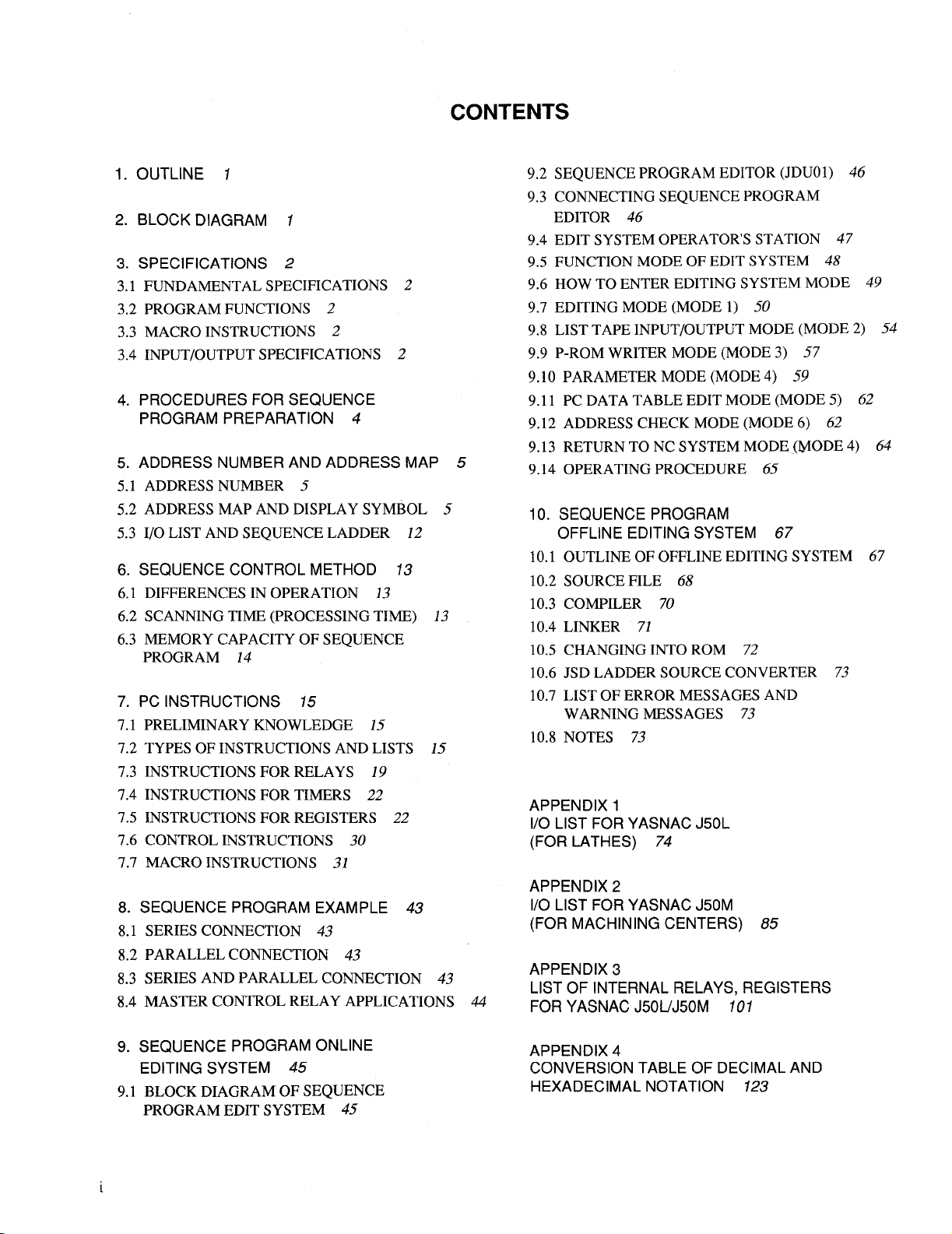
1. OUTLINE 1
2. BLOCK DIAGRAM 1
3. SPECIFICATIONS 2
3.1 FUNDAMENTAL SPECIFICATIONS 2
3.2 PROGRAM FUNCTIONS 2
3.3 MACRO INSTRUCTIONS 2
3.4 INPUT/OUTPUT SPECIFICATIONS 2
PROCEDURES FOR SEQUENCE
4.
PROGRAM PREPARATION 4
5. ADDRESS NUMBER AND ADDRESS MAP 5
ADDRESS NUMBER 5
5.1
5.2 ADDRESS MAP AND DISPLAY SYMBOL 5
5.3 1/0LIST AND SEQUENCE LADDER 12
SEQUENCE CONTROL METHOD 13
6.
6.1 DIFFERENCES IN OPERATION 13
6.2 SCANNING TIME (PROCESSING TIME) 13
6.3 MEMORY CAPACITY OF SEQUENCE
PROGRAM 14
PC INSTRUCTIONS 15
7.
PRELIMINARY KNOWLEDGE 15
7.1
7.2
TYPES OF INSTRUCTIONS AND LISTS 15
INSTRUCTIONS FOR RELAYS 19
7.3
7.4
INSTRUCTIONS FOR TIMERS 22
7.5
INSTRUCTIONS FOR REGISTERS 22
7.6
CONTROL INSTRUCTIONS 30
MACRO INSTRUCTIONS 31
7.7
SEQUENCE PROGRAM EXAMPLE 43
8.
8.1
SERIES CONNECTION 43
PARALLEL CONNECTION 43
8.2
SERIES AND PARALLEL CONNECTION 43
8.3
MASTER CONTROL RELAY APPLICATIONS 44
8.4
9.2
SEQUENCE PROGRAM EDITOR (JDUO1) 46
9.3
CONNECTING SEQUENCE PROGRAM
EDITOR 46
EDIT SYSTEM OPERATOR’S STATION 47
9.4
FUNCTION MODE OF EDIT SYSTEM 48
9.5
HOW TO ENTER EDITING SYSTEM MODE 49
9.6
EDITING MODE (MODE 1) 50
9.7
9.8
LIST TAPE INPUT/OUTPUT MODE (MODE 2) 54
P-ROM WRITER MODE (MODE 3) 57
9.9
PARAMETER MODE (MODE 4) 59
9.10
PC DATA TABLE EDIT MODE (MODE 5) 62
9.11
ADDRESS CHECK MODE (MODE 6) 62
9.12
RETURN TO NC SYSTEM MODE (MODE 4) 64
9.13
9.14
OPERATING PROCEDURE 65
10. SEQUENCE PROGRAM
OFFLINE EDITING SYSTEM 67
OUTLINE OF OFFLINE EDITING SYSTEM 67
10.1
10.2 SOURCE FILE 68
10.3 COMPILER 70
10.4 LINKER 71
10.5 CHANGING INTO ROM 72
10.6 JSD LADDER SOURCE CONVERTER 73
10.7 LIST OF ERROR MESSAGES AND
WARNING MESSAGES 73
10.8 NOTES 73
APPENDIX 1
1/0 LIST FOR YASNAC J50L
(FOR LATHES) 74
APPENDIX 2
LIST FOR YASNAC J50M
1/0
(FOR MACHINING CENTERS) 85
APPENDIX 3
LIST OF INTERNAL RELAYS, REGISTERS
FOR YASNAC J50L/J50M 101
SEQUENCE PROGRAM ONLINE
9.
EDITING SYSTEM 45
BLOCK DIAGRAM OF SEQUENCE
9.1
PROGRAM EDIT SYSTEM 45
APPENDIX 4
CONVERSION TABLE OF DECIMAL AND
HEXADECIMAL NOTATION 123
Page 3
INDEX
Subject
A
ADDRESS CHECK MODE (MODE 6) . . . 4 . . . . . . . . . . . . . . . . .9...9.12 . ...62
ADDRESS MAPANDDISPLAY SYMBOL . . . . .. -....- . .-....5.....5.2 . . . . 5
ADDRESS NUMBER. O.... . . . . . . . . . . . . . . . . . . . . . . . ...5.....5.1 . ...5
,ADDRESS NUMBERANDADDRESS MAP . . . . . . . . . . . . . . . . . . 5 . . . . . . . . . . . . . . 5
APPENDIX 1 I/OLISTFORYASNACJ50L
(FORLATHES) . ..o+. o+.... . . . . . . . . . . . . . . . . . .. APPENDIx 1 . . . . . . . . . 74
APPENDIX21/O LISTFORYASNAC J50M
(FOR MACHINING CENTERS).. . . . . . . . . . . . . . . . . . . .. APPENDIX 2 . . . . . . . . . . 85
APPENDIX 3LISTOF INTERNAL RELAYS, REGISTERS
FoRYAsNAcJ50L/J50M.. . . . . . . . . . . . . . . . . . . . . .. APPENDIX3 . . . . . . . . ..101
APPENDIX 4CONVERSION TABLE OFDECIMALAND
HEXADECIMAL NOTATION. . . . . . . . . . . . . . . . . . . . . . ..APPENDIX4 . . . . . . . . . . 123
B
BLOCKDIAGRAM . . . . . . . . . . . . . . . . . . . . . . . . . . . . . ...2... . . . . . . . . . . . 1
BLOCK DIAGRAMOFSEQUENCE PROGIWMEDITSYSTEM . . . . . . 9 . . . . . 9.1 . . . . 45
c
CHANGING INTOROM . . . . .......~........... . . . . ...10.....10.5 . ...72
CAMPIER .,. SAC....... . . . . . . . . . . . . . . . . . . . . . ...10.....10.3 . ..-70
Compiler Checking Items. . . . . . . . . . . . . . . . . . . . . . . . . ...10.....10.3.3 . ...71
Compiler Operation . . . . . . . . . . . . . . . . . . . . . . . . . . . . ...10.....10.3.1 . ...70
CONNECTING SEQUENCE PROGRAM EDITOR . c . 0 . . . . 0 0 . . 0 . 9 . . 0 . . 9.3 ~. . . 46
CONTROL INSTRUCTIONS.. . . . . . . . . . . . . . . . . . . . . . . . ...7.....7.6 . ...30
D
DIFFERENCES IN OPERATION . . . . . . . . . . . . . . . . . . .. -.. . <6.....6.1 . ...13
E
EDIT SYSTEM OPERATORS STATION . . . . .. C..... . . . . . ...9.....9.4 . ...47
EDITING MODE (MODE 1). . . . . . . . . . . . . . . . . . . . . . . . ...9.....9.7 . ...50
Editing ofPCDataTables . . . . . . . . . . . . . . . . . . . . . . . . ...9.....9.11.1 . ...62
Error ListofCompile . . . . . . . . . . . . . . . . . . . . . . . . . . . . ...10.....10.3.2 . ...70
Execution Files . . . . . . . . . . . . . . . . . . . . . . . . . . . . . . . ...10.... . 10.1.2 . ...67
F
Format ofSourceFile . . . . . . . . . . . . . . . . . . . . . . . . . . . ...10.....10.2.1 . ...68
FUNCTION MODEOFEDITSYSTEM. . . . . . . . . . . . . . . . . . . . . .9.....9.5 . ...48
FUNDAMENTAL SPECIFICATIONS . . . . . . . . . . . . . . . . . . . ., ..3.....3.1 . . . . 2
H
HOWTOENTER EDITING SYSTEM MODE . . . . . . . . . . . . . . . . . 9 . . . . . 9.6 . ...49
I
I/OLISTANDSEQUENCELADDER. . . . . . . . . . . . . . . . . . . . . .5. .<..5.3 . ..”12
INPUT/OUTPUTSPECIFICATIONS. . . . . . . . . . . . . . . . . . . . ...3.....3.4 . . . . 2
INSTRUCTIONS FORREGISTERS . . . . . . . . . . . . . . . . . . . . ...7..... 7.5 .“””22
INSTRUCTIONS FORRELAYS . . . . . . . . . . . . . . . . . . . . . . ...7.....7.3 .“””19
INSTRUCTIONS FORTIMERS . . . . . . . . . . . . . . . . . . . . . . ...7..... 7.4 “-””22
J
JSDLADDER SOURCE CONVERTER . . . . . . . . . . . . ..O---O ““IO. O””” 1O..6 ‘“””73
L
Line Connection . . . . . . . . . . . . . . . . . . . . . . . . . . ..”” ”.. ”10..”” “10.5.2. .””72
LINKER . . . . . . . . . . . . . . . . . . . . . . . . . . . . . . . . . . . . . ..10 .” >--10.4 “’”-71
Linker Operation . . . . . . . . . . . . . . . . . . . . . . . . . . . . . . . .. 10”” ””” 10.4.2 ““’”71
Linker Output File..... . . . . . . . . . . . . ...””” .“”””. ”” .10” ”.”” 10.4.3 ““””72
LIST OFERRORMESSAGES AND WARNING MESSAGES - . “ - “ “ “ 10 “ “ “ “ o 10.7 “ “ “ > 73
LISTTAPEINPUT/OUTPUTMODE (MODE2)”””.””....OC”. .“ 9“”””” 9.8 ““””54
M
MACRO INSTRUCTIONS . . . . .--.-””...”.””””-” ““” ”””” 3””” ””3.3 ““””2
MACRO INSTRUCTIONS.. . . . . . . . . . . . . . . ...4 ‘o oooo. oo7. -4””7.7 ““””31
MASTER CONTROL RELAYAPPLICATIONS ‘“ -. --”” ”””” O”””” 8“”-o. 8.4 ““””44
MDIWrite Operation on Sequence Program. . . . “ . . ““ “ “ ““ “ “ “ “ 9 .- . “ “ 9.7.2 “ “ “ “ 52
MEMORY CAPACITY OFSEQUENCE PROGRAM O.. -”o”o o-o ‘.. 6...”” 6.3 “’””14
N
NOTES . . . . . . . . . . . . . . . . . . . . . . . . . ...””” .“”””. ”””lO. ””. ”10.8 ““””73
o
Object Data and Linker Processing ......o”””.””””””. .. ”. 10”” ”” .10.4.1 ““””71
Operation Environment”.” ‘.-””-”””””-””””””” ““” ”” ”” 10”” ””” 10.1.1 ‘“””67
OPERATING PROCEDURE.. ...<..”..”””””””.”. ““” ”.”” 9.”. ””9.14 ““..65
OUTLINE .0000 OOC” O.’.. “$. .O. O-”.-””””””-””” “oolo-””o.oo-o””o-el
Outline ofExecution File Processing ““””.””...””.”-.”” .o-10.””..10.1.3 ““”.67
OUTLINE OFOFFLINEEDITING SYSTEM .“””””” ”.”” ””. .””10. .“” .10.1 .“67
Outline of Operation .”... .“...””.””””””.”.” “.” ”” ”” lo”””. -10.1.A ““””67
Chapter Section Page
Page 4
INDEX (Cent’d)
Subject
P P-ROM Format Tape Input/c) utput Function ( ~ , m )
P-ROMWRITER M0DE(M0DE3) . . . . . . . . . . . . . . . .
PAWLLEL CONNECTION . . . . . . . . . . . . . . . . . . . . . .
PARAMETER MODE (MODE 4)... . . . . . . . . . . . . . . . .
PC DATA TABLE EDIT MODE.. .................
PC INSTRUCTIONS . . . . . . . . . . . . . . . . . . . . . . . . .
PRELIMINARY KNOWLEDGE. . . . . . . . . . . . . . . . . .
PROCEDURES FOR SEQUENCE PROGRAM PREPARATION .
PROGRAM FUNCTIONS . . . . . . . . . . . . . . . . . . . . . . .
R Reading-in, Punch-out, and Verify a P-ROM Format Tape
(IN, OUTand VERoperations) . . . . . . . . . . . . . . . . . . .
REIWRN TO NC SYSTEM MODE (MODE 4) . . . . . . . . . . .
S SCANNING TIME (PROCESSING TIME) . . . . . . . . ~ . . . .
Selection of PROM Writer... . . . . . . . . . . . . . . . . . . .
SEQUENCE CONTROL METHOD . . . . . . . . . . . . . . . . .
Sequence Program Editing . . . . . . . . . . . . . . . . . . . . .
SEQUENCE PROGRAM OFFLINE EDITING SYSTEM . . . . .
SEQUENCE PROGRAM ONLINE EDITING SYSTEM . . 0 . . .
SEQUENCE PROGRAM EDITOR (JDUO1) . . . . . . . . . . ~ .
SEQUENCE PROGRAM EXAMPLE . . . . . . . . . . . . . . . .
SERIES AND PARALLEL CONNECTION . . . . . . . . . . . . .
SERIES CONNECTION . . . ..-. . . . . . . . . . . . . . . . .
SOURCE FILE . . . . .. O...... . . . . . . . . . . . . . .
SOURCE FILES . . . . .. O..... . . . . . . . . . . . . . .
SPECIFICATIONS . . . . . . . . . . . . . . . . . . . . . . . . . .
T TYPES OF INSTRUCTIONS AND LISTS . 0 . . . . . . . . . . . .
W When NC Unit Entered SD Mode from Offline State . . . . .
When NC Unit Entered SD Mode from Online State . . . . .
When NC Unit is in Offline State (System No.6 + SD MODE) c , . . 9 . . . . . 9.6.1 . . . ~ 49
When NC Unit is in Online State (System No.4 + SD MODE) . . . . 9 . . . . . 9,6.2 . . . . 49
Chapter Section
. . . . . . . . . . .
. . . . . . . . . . .
. . . . . . . . . . .
. . . . . . . . . . .
. . . . . . . . . . .
. . . . . .
. . . . . . . . . . .
. . . . . .
. . . . . . . . . . .
. . . . . . . . . . .
. . . . . . . . . . .
. . . . . . . . . . .
. . . .
. . . . . .
. . . . . . . . . . .
. . . . . .
. . . . . .
. . . . . . . . . . .
. . . . . .
. . . . . . . . . . .
. . . . . .
. . . . . .
. . . . . .
. . . . . .
. . . . . . . . . . .
. . . . . . . . . . .
. . . . . . . . . . .
9
9
8
9
9
. . . . . . . . . .
7
7
4 . . . . . . . . . . .
3
9
9
6
. .10.....10.5.1 . ...72
6.. .’ . . . . . . ..”13
9
10..............67
9..............45
9
. . . . . . . . . . . . . .
8
8
8 . . ...8.1 . ...43
10 . . ...10.2 . ...68
10 . ...10.2.2 . ...68
3 ., . . . . . . . . ...2
7
9
9
9.7.3
9.9
8.2
9.10
9.11
7.1
3.2
9.11.2 . . . 62
9.13 ..64
6.2 . ...13
9.7.1 “ . . . 50
9.2 . ...46
8.3 . ...43
7.2 . ..15
9.13.1 . . . . 64
9.13.2 . . . . 64
. . . .
. . . .
. . .
. . .
. . . .
. . . .
. . . .
. . . .
. . . .
Page
53
57
. 43
. 59
62
15
15
4
2
43
...
111
Page 5
1. OUTLINE
1. The programmable controller (called PC hereafter) for
YASNAC J50L/J50M stands between the standard
YASNAC NC unit and the machine tool. It facilitates
the compact and efficient utilization of the sequence
control required by the machine tool through the software.
2. Sequence program editing of PC can be performed efficiently with CRT”; NC and JSD modes are easily
changed and selected.
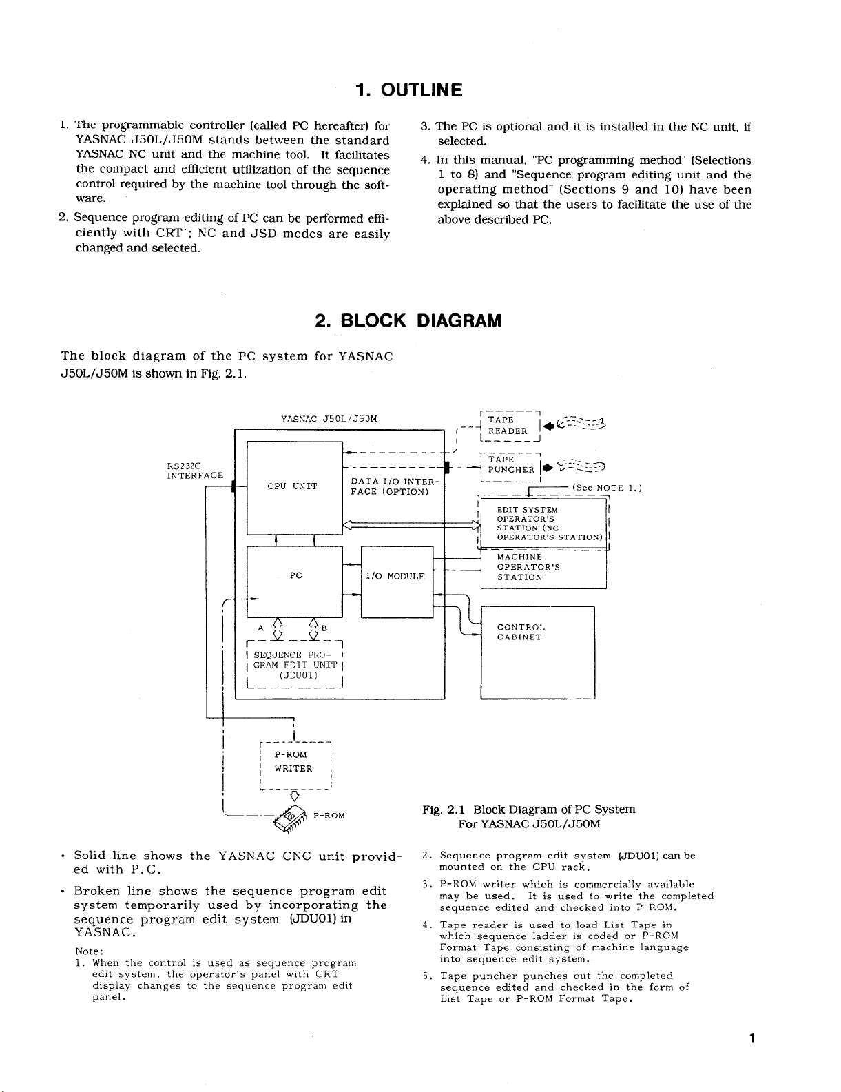
2. BLOCK DIAGRAM
The block diagram of the PC system for YASNAC
J50L/J50M is shown in Fig. 2.1.
YASNAC J50L/J50M
——_ ___ ___ _/
RS232C
INTERFACE
CPU UNIT
n-”-” ----- ‘,
DATA 1/0 lNTER FAcE (OPTION)
3. The PC is optional and it is installed in the NC unit, if
selected.
4. In this manual, “PC programming method” (Selections
1 to 8) and “Sequence program editing unit and the
operating method” (Sections 9 and 10) have been
explained so that the users to facilitate the use of the
above described PC.
~–———–7
,--4
~=:: j
——-—
- +’ %;~HERj* f5~23
L_____J
r :D’= ~y~TEM
● c5’’$~-3
_~_(See NOTE 1.)
1
I
1/0 MODULE
r
-k----n
Solid line shows
ed with P.C.
Broken line shows the sequence program edit
sYstern temporarily used by incorporating the
sequence program edit system (JDUO1) in
YASNAC.
Note:
1. When the control is used as sequence program
edit system, the operator’s panel with CRT
display changes to the sequence program edit
panel.
the YASNAC CNC unit provid-
‘M~CHINE
OPERATOR’S
STATION
—————
J
Fig. 2.1 Block Diagram of PC System
For YASNAC-J50L/J50M
Sequence program edit system (JDUO1) can be
2.
mounted on the CPU rack.
P-ROM writer which is commercially available
3.
may be used.
sequence edited and checked into P-ROM.
4.
Tape reader is used to load List Tape in
which sequence ladder is coded or P-ROM
Format Tape consisting of machine language
into sequence edit system.
5,
Tape puncher punches out the completed
sequence edited and checked in the form of
List Tape or P-ROM Format Tape.
It is used to write the completed
Page 6
3. SPECIFICATIONS
3.1 FUNDAMENTAL
Control method:
(1)
(2) Processing time:
Approx. 2.7 l.i seclstep
qigh speed scanning time - 8 msec
Low speed scanning time - 8 msec x n (n is
determined by the capacity of the total
program. )
(3) Program memory capacity :
Memory element :
Basic – 64 k bytes (1 EPROM)
(64 k bytes corresponds to approximately 16000 steps
in basic instruction.)
(4) Types of instruction language:
Basic instruction – 59 types
Macro instruction – 11 types
PROGRAM FUNCTIONS
3.2
Internal relay:
(1)
(2) Register:
(3) Timer:
. 8 msec - 2.4 see, 20 ea.
.
50 msec - 12.75 see, 30 ea.
. 100 msec - 25.5 see, 30 ea.
.1
sec –
.1
min
(4)
Sequencer parameter: 100
Keep relay:
(5)
Keep memory:
(6)
3.3
Following 11 types of macro instructions can be
used.
255 sec , 10 ea.
- 255 rein, 4 ea.
MACRO INSTRUCTIONS
SPECIFICATIONS
Scanning method
EPROM (1024 k bits/one)
4000 points
500 (8 bits/one)
94 (5 types)
7200
900 (8 bits/memory)
(6) Pattern clear
(7) Parity check
(8) Data conversion:
(9) Data search
(10) Index data transfer
(11) Message display
3.4
lNPUT/OUTPUT SPECIFICATIONS
(1) Standard 1/0 boards
< FC81O (FC860) >
(i) DC input:
(ii) Non contact output : 96 points
< FC861 >
(i) DC input:
(ii) Non contact output: 56 points
(2) CRT panel built-in 1/0 boards
< SP50-1 >
(i) DC input:
(ii) Non contact output : 32 points
< SP50-2 >
(i) DC input:
(ii) Non contact output : 56 points
Note:
1. The detail of basic instructions are given
in the following table.
Type of Instruction
Relay instruction
1.
2. Register instruction
3. Timer instruction
4. Control instruction
112 points ‘
64 points
64 points
64 points
SUBP 009
SUBP 011
SUBP 014
No. of
Instructions
I
I
SUBP 017
SUBP 018
SUBP 023 -Optional
function
13
37
2
7
Instruction word
(1) Rise signal detection:
(2) Fall signal detection:
(3) Counter:
?unctions--Ring counter or preset counter or
lp-down counter.
Zounting range --O - 9999
Rotation
[4)
Code conversion
(5)
SUBP 003
SUBP 004
SUBP 005
SUBP 006
SUBP 007
2
Tot al
Internal relays and registers are the same.
2.
Addresses used as internal relays cannot be
used as internal relays.
Keep relays and keep memories are the same.
3.
Addresses used as keep relays cannot be used
as keep memories.
memories cannot be used as keep relays.
I
Addresses used as keep
59
Page 7
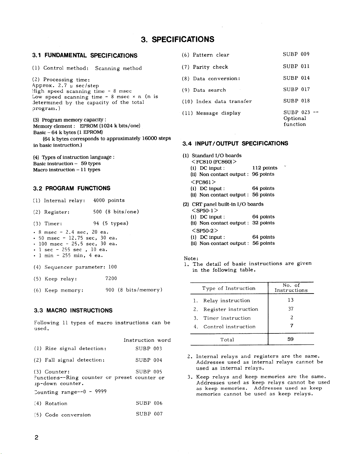
(3) 1/0 board location
5 1/0 boards are shown below,
YASNAC J50L/J50M
-.—.7
r-=
PC BOARD
JANcI)-PCVI
CNIZ
G
CRT PANEL
;OARD CRT -1
I
CN13
!
L--
J
..— - --l
STANDARD I/O BOARD
CNICN2CN3CN40+5CN6
(FCMJO) I
~
STANDARD 1/0 BOARD
-—-
JANCD-FC861
LNI 1
L5-
rub-d
(4) Maximum number of each 1/0 board
Maximum
“ Standard 1/0 board 3
(FC81O, FC860)
. Standard 1/0 board 7
(FC861)
“ CRT panel butlt-in 1
1/0 board
(SP50- 1)
Input :
Output : 288 points
Input :
Output : 392 points
Input :
Output : 32 points
(56 points for SP-2)
1
INPUT :
INPUT :
INPUT :
OUTPUT :
INPUT :
INPUT :
INPUT :
INPUT :
OUTPIJT ;
336 points
448 points
64 points
24 POINTS OUTPUT :
24 POINTS
16 POINTS
32 POINTS
40 POINTS
40 POINTS
24 POINTS OUTPUT :
8 POINTS
40 POINTS
OUTPUT :
OUT PUT :
OUTPUT :
16 POINTS
16 POINTS
24 POINTS
(FOR SP50-2 )
16 POIITI’S
8 POINTS
Notes :
YASNAC J50 needs at least 1 of CRT panel built-in 1/0 board
.
(SP50-1 or SP50-2). Therefore, a max. of 3 (max. input : 400
points,max.output: 344 points)for adding onlyFC810/FC860
and a max. of 7 (max. input : 512 points, max. output : 448
points)foraddingonfyFC861can be connected.
. Several1/0boardscan exist atthe same time,withoutexceeding
the allowance1/0area No.
.The numberof 1/0boards can be expanded. Therefore,the last
board needsto be terminalscanned.
3
Page 8
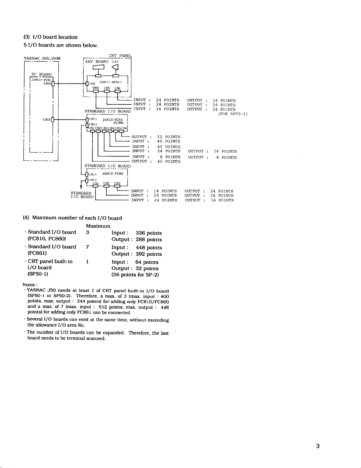
4. PROCEDURES
c
Determine the specifications
controlled operation .
of
L
I I
\Carry out assignment of ]
input loutput signals be–
tween machine tool and PC.
Start
I
I
i
FOR
)
SEQUENCE PROGRAM PREPARATION
,_. - —
a
Q
I
I
I
Complete test operation for
+,
i
NEED
I
I I
==+-
-+=
Perform coding by instruc-
tion language of PC.
Formulate the list tape by
the tape puncher.
T-4- -
Input the list tape through
the tape reader.
I
,— -—----- .-- .-—-- _______ \
Store the sequence program
of P-ROM format (Machine
language) in RAM memory.
1
lF-
7
—.— .—
.——
.
t
I
–1
I
I
I
I
I
-—~---l
~______ A__. __-7
I Key–in the list
! the sequence edit ,
1
operator’s station.
T ~______ .__. _.. __J
L ——— -—
-1
from I
Write the sequence program
through the connected,
I
I
P-ROM writer.
I
Mount the P-ROM to PC.
1
I
Complete final test run
through the contents of
P-ROM.
I
I
1 I
I
I
I I ——
Perform editing of the se-
quence program while watch-
ing the display on the CRT
(delete, input, change) . ,
(
I
— .
1
Note: The sections surrounded by~ .- -;req~re the
a
u
—— —
i
J
End
—
IComplete final correction of I
the sequence ladder (1/0
*
I
“sequence program editing device
- –+– -
I
(JDUO1).”
J
I
Page 9
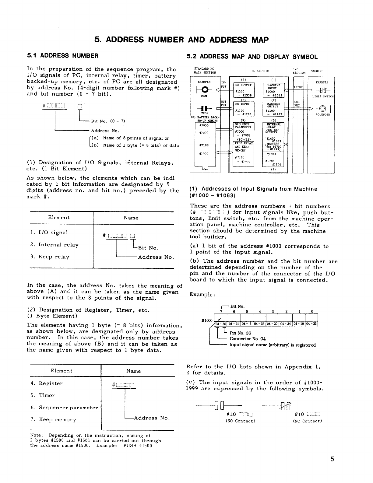
5. ADDRESS NUMBER AND ADDRESS MAP
5.1 ADDRESS NUMBER
In the preparation of the sequence program, the
1/0 signals of PC, internal relay, timer, battery
backed-up memory, etc. of PC are all designated
by address No. (4-digit number following mark #)
and bit number (O - 7 bit) .
I
~ Address No.
(1) Designation of 1/0 Signals, IfiternaI Relays,
etc. (1 Bit Element)
As shown below, the elements which can be indi-
cated by 1 bit information are designated by 5
digits (address no. and bit no. ) preceded by the
mark #.
Element
1. I/0 signal
2. Internal relay
3. Keep relay
In the case,
above (A) and it can be taken as the name given
with respect to the 8 points of the signal.
(2) Designation of Register, Timer, etc.
(1 Byte Element)
The elements having 1 byte (= 8 bits) information,
as shown below,
number.
In this case, the address number takes
the meaning of above (B) and it can be taken as
the name given with respect to 1 byte data.
-Bit No. (O - 7)
(A) Name of 8 points of signal or
(B) Name of 1 byte (= 8 bits) of data
[
,..,.,..,.;
L
Name
T
Bit No.
Address No.
I
# ,-..,,,,7 :;
the address No. takes the meaning of
are designated only by address
5.2 ADDRESS MAP AND DISPLAY SYMBOL
STANDARD Nc
MAIN SECTION
F+EEIm
+& ‘ ~
1) 8ATTE4YB/Lx-,
ED-UP ~RY
#7000
1
#7099
#7100
#7:99
e =
I
OUT-
,
~
>
>
~c ;;:”T
#lZoo
- #1295
(9)
SEQUENCE
PABAMETER
#7000
– #7099 -
(10)(11)
KEEP REMY
AND KEEP
MQIORY
#7100
– #7999
pc 5EcT10N
rl
!GISTER
,(Except
#1700
1
2
K4~:;E
#1100
– #1162
(5)
IfWE9NAL
RELAY
AND RE-
11400
– #1999
fOr#1700
- #1799[
TIMER
- #1799
(7)
1/0
SECTION
wu
—
—
UTUT
.
.
—
MACHINE
EXAMPLE
~+HF
LIMIT SWITC
‘w
SOLENOID
(1) Addresses of Input Signals from Machine
(#1000 - #1063) These are the address numbers + bit numbers
(# ,-.-.,7 ..,.
......... ...... ) for input signals like, push but-
tons, limit switch, etc. from the machine oper–
ation panel, machine controller, etc.
This
section should be determined by the machine
tool builder.
(a) 1 bit of the address #1000 corresponds to
1 point of the input signal.
(b) The address number and the bit number are
determined depending on the number of the
pin and the number of the connector of the 1/0
board to which the input signal is connected.
Example:
~ BitNo.
76543,21 0
# 1000
04-3SIQ4-21104-51M-35[M- miM-MIM-19]M-w
L PlnNo. 36
l-!
ConnectorNo.04
Inputslgmdname(arbitrary)is registenxl
Element
4. Register
I
Name
# ~,r-,,-,r,
. .L.,L.,L.,
5. Timer
T
6. Sequencer parameter
7. Keep memory
I
1
Depending on the instruction, naming of
Note:
2 bytes #1500 and #1501 can be carried out through
the address name #1500, Example:
I
~A&essNo,
PUSH #1500
Refer to the 1/0 lists shown in Appendix 1,
2 for details.
(c) The input signals in the order of #1000-
1999 are expressed by the following symbols.
5
Page 10
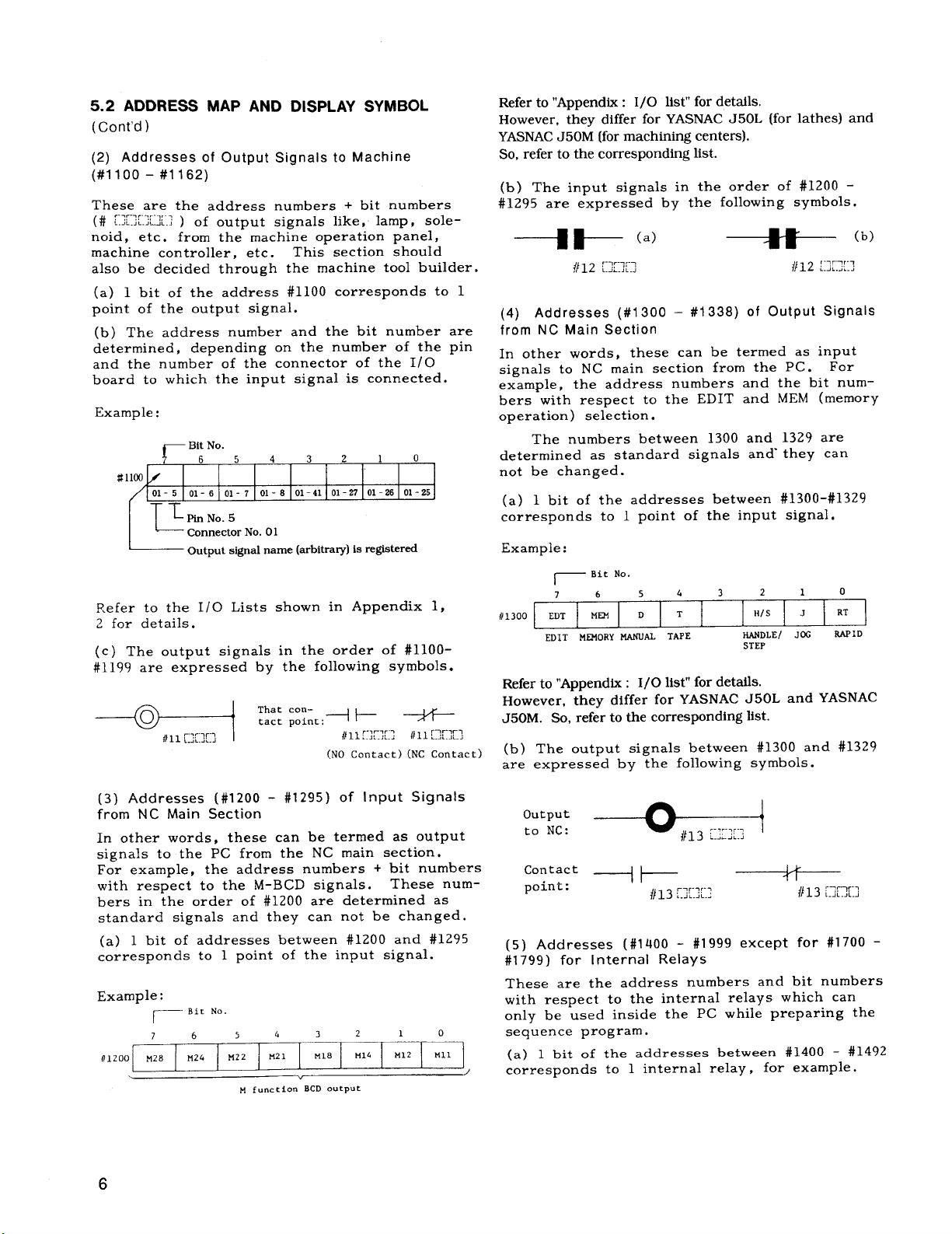
5.2 ADDRESS MAP AND DISPLAY SYMBOL
(Cent’d)
(2) Addresses of Output Signals to Machine
(#1100 - #1162)
These are the address numbers + bit numbers
(# rfi[~d[.~ ) of output signals like, lamp, solenoid, etc.
machine controller, etc.
from the machine operation panel,
This section should
also be decided through the machine tool builder,
(a) 1 bit of the address #1100 corresponds to 1
point of the output signal.
(b) The address number and the bit number are
determined, depending on the number of the pin
and the number of the connector of the 1/0
board to which the input signal is connected.
Example:
- BitNo.
?6543210
#llw
01-5101-6101-7101-8101-41 101-27101-26101-25
~PinNo.s
ConnectorNo.01
Lk
Outputsignalname(arbitrary)is registered
Refer to the I /O Lists shown in Appendix 1,
2 for details.
(c) The output signals in the order of #1100 #1199 are expressed by the following symbols.
Refer to “Appendix: 1/0 list” for details.
However, they differ for YASNAC J50L (for lathes) and
YASNAC J50M (for machining centers).
So, refer to the corresponding list.
(b) The input signals in the order of #1200 #1295 are expressed by the following symbols.
_’+ fl— (a)
(4) Addresses (#1300 - #1338) of Output Signals
from NC Main Section
In other words, these can be termed as input
signals to NC main section from the PC.
For
example, the address numbers and the bit numbers with respect to the EDIT and MEM (memory
oPeration) Selection.
The numbers between 1300 and 1329 are
determined as standard signals and they can
not be changed.
(a) 1 bit of the addresses between #1300 -#1329
corresponds to 1 point of the input signal.
Example:
~ Bit No.
2 1
H/S J
RANDLE/ JOC
STEP
#1300
6 5
7
EDT MEM
ME210RYMANUAL TAPE
EDIT
4 3
T
D
Refer to “Appendix : 1/0 list” for details.
However, they differ for YASNAC J50L and YASNAC
J50M. So, refer to the corresponding list.
0
RT
RAPID
(3) Addresses (#1200 - #1295) of Input Signals
from NC Main Section
ln other words, these can be termed as output
signals to the PC from the NC main section.
For example, the address numbers + bit numbers
with respect to the M-BCD signals.
These num-
bers in the order of #1200 are determined as
standard signals and they can not be changed.
(a) 1 bit of addresses between #1200 and #1295
corresponds to 1 point of the input signal.
Example:
Bit No.
#lZoo
7
M28
6
M24
4 3
5
M21
U22
v
functionBCD output
M
M18
2 1 0
)412 Ml 1
M14
I
6
(b) The output signals between #1300 and #1329
are expressed by the following symbols.
(5) Addresses (#1400 - #1999 except for #1700 -
#1799) for Internal Relays
These are the address numbers and bit numbers
with respect to the internal relays which can
only be used inside the PC while preparing the
sequence program.
1/
(a) 1 bit of the addresses between #1400 - $1492
corresponds to 1
internal relay, for example.
Page 11
1/0 list example:
(c) In a register,
.
pression symbol.
examples of the symbols.
the address itself is the ex-
The following shows two
“l400-
(b) The number of usable internal relays are as
follows .
500 bytes
(c) The internal relay and its contact
expressed by the following symbol.
There is no limit for NO and NC contact Doints
until the program memory capacity is exceeded.
(d) Adressed used in register cannot be used as
internal relay.
(6] Addresses (#1400 - #1999 except for
#1700 - #1799) of Register
These are the address numbers with respect to
the 1 byte (= 8 bits) register for general
purpose use.
. .
register instruction or for the working addresses
of macro instructions.
(a) 1 address number
of 1 byte.
1/0 list example:
//1500
#1501
~ Write the internal relay
name (arbitrary)
x 8 bits = 4000 relays
point are
These registers are used for
corresponds to 1 register
4
Insert the name (arbitrary)
of the register
t-+l?l
b
(d) Addresses used in internal relay cannot be
used as register.
(7) Addresses of Timer (#1700 - #1799)
These are the addresses with respect to the
timers. They are used in the instruction of
timers.
(a) 1 address number corresponds to 1 timer,
1/0 list example:
#1700
//1701
(b) The time unit and the number of usable timers
are shown in the following table.
Address No.
#1700-#1709, #1’760-#1769
#1710-#1729, #1790-#1799
#1730-#1749, #1780-#1789
#1750-#1759
#1770-#1773
The range of set values is O- 255.
(O- 127 for variable timer.)
(c) The symbol example of timers is given below.
Example:
[fl
!
Insert the name Insert the set
of the timer
#15cJn
#15ncl
No. of
timers
I
!
I
20
3,0
30
10
4
<i
,t
J
value, etc.
Time unit
1 = 8 msec
1 = 100msec
1 = 50
msec
l=lsec
l=lmin
(b) Number of usable registers are as follows:
500 registers from #1400 to #1999 except for
#1700 tG #1799.
l-w1
LTimer instr~c- L set value of
tion (2 types)
#17Kln,DnH
I
timer (Hexadecimal)
7
Page 12
5.2 ADDRESS MAP AND DISPLAY SYMBOL
(Cent’d)
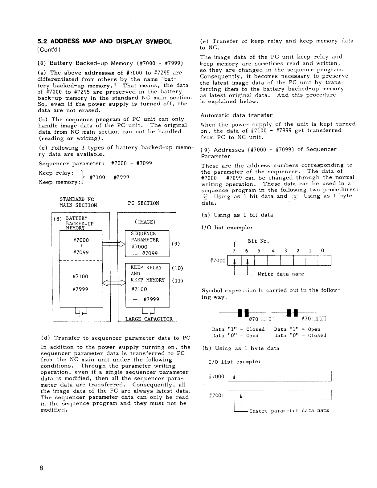
(8) Battery Backed-up Memory (#7OOO - #7999)
(a) The above addresses of #7ooO to #7295 are
differentiated from others by the name “bat-
tery backed-up memory. ”
of #7000 to #7295 are preserved in the battery
back-up memory in the standard NC main section.
So, even if the power supply is turned off, the
data are not erased.
(b) The sequence program of PC unit can only
handle image data of the PC unit.
data from NC main section can not be handled
(reading or writing).
(c) Following 3 types of battery backed-up memo-
ry data are available.
Sequencer parameter: #7000 - #7099
Keep relay:
Keep memory:J
STANDARD NC
MAIN SECTION
) BATTERY
BACKED-UP
MEMORY
I F
+-----------1
L
#7100- #7999
1
{/7000
#7;99
1
I
That means, the data
The original
PC SECTION
F
SEQUENCE
PARAMETER
#7000
P
&
KEEPMEMORY
#7100
H
(9)
(lo)
(11)
I-J
(e) Transfer of keep relay and keep memory data
to NC.
The image data of the PC unit keep relay and
keep memory are sometimes read and written,
so they are changed in the sequence program.
Consequently, it becomes necessary to preserve
the latest image data of the PC unit by transferring them to the battery backed-up memory
as latest original data.
is explained below.
Automatic data transfer
When the power supply
on, the data of #7100 from PC to NC unit.
(9) Addresses (#7000 -
Parameter
These are the address numbers corresponding to
the parameter of the sequencer.
#7000 - #7099 can be changed through the normal
writing operation.
sequence program
a~ Using as 1 bit
data.
(a) Using as 1 bit
1/0 list example:
r ‘it
76543210
#7000
Symbol expression is carried out in the follow-
ing way.
dtl
~ Write data name
And this procedure
of the unit is kept turned
#7999 get transferred
#7099) of Sequencer
The data of
These data can be used in a
in the following two procedures:
data and (~,
data
No.
Using as 1 byte
I
(d) Transfer to sequencer parameter data to PC
In addition to the power supply turning on, the
sequencer parameter data is transferred to PC
from the NC main unit under the following
conditions. Through the parameter writing
operation, even if a single sequencer parameter
data is modified, then all the sequencer parameter data are transferred.
the image data of the pC are always latest data.
The sequencer parameter data can only be read
in the sequence program and they must not be
modified.
8
Consequently, all
Data “l” = Closed
Data “O” = Open
(b) Using as 1 byte data
1/0 list example:
/7000
1A
UI~sert parameter data name
Data “l” =
Data “O” = Closed
Open
Page 13
The symbol expression is the address number.
The example of using in timer is shown in the
following figure,
Example:
l177il, #70 ::7::
t+y~
Variable timer
instruct ion
Timer setting
by parameter
‘
I address number beyond #7100 corresponds to
(a)
one
keep memory of 1 byte (8 bits).
list example:
1/0
//71061 ~
~Write the name of the
keep memory
I
(10) Addresses (#7100 - #7999) of Keep Relay
These are the address numbers and bit numbers
of the keep relays used in the PC.
(a) I bit of #7100 - #7999 corresponds to 1 keep
relay.
1/0 list example:
➤Bit No.
7654321 0
“7100P==@===
‘Write the name of the keep relay
(b) The number of usable keep relays
follows .
900 bytes
(c) The keep relays and their contact
are
expressed by the following symbols.
x 8 bits = 7200
a’ ————0—+
is as
points
(b)
The number of usable kee~ memorv is as
follows :
900 memories from #7100 to #7999
(c) The address number itself stands for the
symbol of the keep memory.
MOV
l+ I‘1 ‘
MOV :
to keep memory #71zK~
(12) Writing Initial Values of Keep Relays and
Keep Memories
When preparing a sequence program by using
the keep relays and keep memories, it becomes
necessary to set the initial values prior to
the execution.
(a). Set the system number switch of NC unit at
11111and then turn on the power supPIY.
(b) Depress the [=1 function key.
displayed on the CRT screen:
(c) After keying-in in the order of ~~ [1 ‘@ ~,
if the cursor key is depressed, then the following
display will be o-btaine~.
Transfer the contents of register #1500
Input/output signal ON/OFF state will be
#1500, #713::
‘
(NO Contact)
(11) Addresses (#7100 - #7999)
These are the addresses corresponding to the 1
byte memory which can be preserved even after
turning off the power supply.
formance is limited only to the preservation of
data, the keep memory can be used in the same
way as that of a register, Consequently, the
keep memory can also be used as an object of
register instruction or as supplementary data
of macro instruction.
preparing a sequence program for memory random
type ATC, this keep meinory becomes necessary.
Especially, when
(NC Contact)
If the per-
Cursor
DIAGNOSIS
OPEN 1:
O:
76543210
#710000000000 o
I
;//710100001000 8
7710200000000 0
‘77103 OOOOO1O1 5
t
#710411111111
/710800000000 o
#710900011000
00000 NOOOO
255
CLOSE +2____
RDY
- Bit No.
Decimal
- display
9
Page 14
5.2 ADDRESS MAP AND DISPLAY SYMBOL
(Cent’d)
(d) Adjust addresses #7105 to #7294 for initial
condition setting by depressing the cursor.
(e) If the -] (insert) key is depressed,
the cursor will move in the right hand direction,
and will move to the 7th bit position of the
address.
(f) Keep on pressing the cursor key until it
becomes adjusted to the position of the decimal
display.
(g) Key-in the desired values (O - 255) for set-
ting initial condition and then depress the
key. The decimal display will get changed to
the presently keyed in value.
(h) If the
_ key is depressed, the cursor
will move to the left hand position #.
the setting of one address number is completed.
(i) Repeat steps (d) to (h) to write all the
desired initial values of the address numbers,
(j) Adjust the system number switch to “O. “
m
Thereby,
(a) Keep memory display
Following displays are added to existing #7100 #7499 display:
Depress function key
Key-in ❑ , ❑ , ❑ , ❑ and depress cursor ~ .
12GN
G
.
L-l
CRT screen has display as shown in either Fig. (i)
or (ii) .
[Hereafter Fig. (i) is to be called 2-digit display,
while Fig. (ii) is to be called 4-digit display. ]
DIAGNOSIS ._-_____= ._~OOOO ‘0000
‘L--~:N-O____-_____!-??: ‘--–---”
.--_:#8600:
:#8601:
1
;r--l
,#860211(001)1
h8693j(O02)~
;#86041fiO03)~ :05;
I -~-J 1
;#86051 ‘ loo;_______
;#8606 ;
1
I
L------- -—-1
I
r-l
1o11
1
!02:
;03;
,04;
la SET T~
DIGIT
Fig. (i) #6022 D2=0 #6355=8602
- POT NO, TITLE
.-POT NO.
- KEEP MEMORY
#6356=8604
Note:
If a particular bit is desired to be
changed O Z 1, carry out following operations
after the operation of item 5) .
Depress the
cursor key and adjust the cursor to the bit
desired to be changed, then depress ~ key.
0=
1 change will be obtained.
1:
0 change will be obtained if the ~ key
is depressed again.
(13) Writing of Keep Relay Numerical Input
(Optional only for J50M)
Writing to keep memory (#7100 - #7999)
can be
normallv executed from O to 255, however, 4-digit
writing’ is also possible with numbers #860”0 - -
#8999.
to each other as shown in the figure below.
#7100 - #7499 and #8600 - #8999 correspond
#7101
is altered by writing and alteration of #8601.
I’iote: When keep memory is referred
from sequence, use #7100 - #7499,
not #8600 – #8999.
Z8600
*71OO
I
$8601
37101
I
I
aa999
L
:
IT7499
DIAGNOSIS
[:-:N]::__ _ ___ __T_-w.r - ‘- ‘- - -
----l#8600[
[#86011
1#8602~(001)
I#8603;
;#8604; (002)
j#86051
:#8606;
I
----- --- .-— ~
I
ltiNio91_____ –______ __ –--.___!-.
Fig. (ii) #6022 D2=1 #6355=8602
00000 NOooo
----
,,
!02011
I
II
I
,0403+SET T4
DIGIT
!,
t
I
II
105051
II
1;
,
100001
L-—J
POT NO. TITLE
-KEEP MEMORY NO.
#6356=8604
For Fig. (ii) , even and uneven number keep memories are used in pairs, O
to 9999 are available
by expressing the higher 2 digits of the decimal
4 digits with even No. keep memory, and lower 2
digits with uneven No. keep memory.
Pot No, display [Figs. (i) , (ii)]
When the max. and min.
set to parameters
#6355 and #6356, Figs. (i) and
keep memory numbers are
(ii) show how #6355 and #6356 are set for #7402
#8604, respectively.
and
(b) Writing to keep memory
Turn system No. switch to “ 1“ .
Use page cursor keys ~ and ~ to move the
cursor to keep memory No. to be changed. Input
new figure and depress WR key.
on
Procedure mentioned above enables #8600 - #8999 range data to
be changed and set.
10
Page 15
Notes:
.
The same memory is used for #8600 - #8999 and
#7100 - #7499: if a value of #8602 is changed,
that of #7102 is changed to the same value.
.
When the display can be extended up to 9999,
as in Fig. (ii), the even number keep memory
data are changed to one lower number and
cursor moves there by writing when the cursor
is at an uneven keep memory number.
.
If #6355 and #6356 are set conversally, pot No.
title and pot No.’ are not normally displayed.
However, if #6355 and #6356 have keep memory
No. on the same page, pot No. title is displayed,
[Refer to Fig. (iii).]
.
If uneven number is set by mistake for #6355
when 4-digit display (#6022 D2=1), pot No. is
displayed from the even number keep memory
No. which is one number higher than the pot
No.
DIAGNOSIS 00000 NOOOO
@~::____-____ T-_ N@+---
#8600
#8601
#8602
#8603
# 8604
#8605
#8606
#8609
Fig
. (iii) #6022 D2=0 #6355=8604 #6356=8602
-. ---— ------ .
01
02
03
04
05
06
07
09
-.
POT NO.
TITLE
r DIAGNOSIS
P-NO
?$8600(010)
?48601(011)
#8602 (012)
L
Fig.
(V) #6022 D2=0 #6355=7391
. When pot
#6355 and
● In 2-digit display (#6022 D2=O), writing-in
number is not displayed, set O for
#6356.
00000NOOOO
T-No
01
02
03
4
1
more than a 3-digit number is not accepted.
(14) Address Setting of 1/0 Board
1/0 board has a rotary switch for address setting. For
rotary switch and address, refer to the table below.
(a) Standard 1/0 Board
‘C660
FC810
1/0AreaNo.
1
2
Input
#1000
#1813
#1016
to
#1029
#1032
#1:45
3utput
#lloo
to
#1111
#1116
to
#1127
#1132
to
#1143
1/0
AreaNo.
1-1
1-2
2-1
2-2
FC861
Input
#1000 #lloo
to
#
1007 #1106
$1008
to
#lo15
#1016 #1116
to
#
1023 #1122
#1024
to
#lo31
#1032
output
to
#1108
to
#1114
to
#1124
to
#l130
#1132
DIAGNOSIS
P-NO
#8600
#8601
#8602
#8603
#8604 (001)
#8605
#8606 (002)
#8609
00000Noooo
T-NO
0201
0403
0805
0807
Fig. (iv) #6022 D2=1 #6355=8603 #6356=8606
.
If a number lower than that for #6355 is set for
#8600, pot number from #8600 is lower than the
number already set to display. [Refer to Fig.
(v). ]
#1046
#1061
#1148
to
to
#1159
For rotary switch (SW1) setting and 1/0 area No., refer to
the table below.
Swl
o
I
1
2
3
4
I
5
—
I
6 3-2
7
8
Q
:0
F
I
1/0Area No.
FC861
Nosetting
1-1
1-2
2-1 2
2-2
3-1
4-1
4-2
No setting
FC8lo/Fc860
Nosetting
1
setting
No
setting
No
3
No setting
4
No setting
11
Page 16
5.2 ADDRESS MAP AND DISPLAY SYMBOL
~Cont’d)
(b) CRT Panel Buik-in I/O Board
SP50
Area No.
1/0
1-1 #looo to #loo7
1-2
2-1
2-2
3-1
3-2
4-1
4-2
I
,
I
InDut
#1008 to #1015
#1016 to #1023
#1024to #1031
#1032 to #1039
#lo40 to #lo47
#1048 to #1055
#1056to #1063
For rotary switch (SW1) setting and 1/0 area No., refer to
the table below.
31 2-1
4
5
6
2-2
3-1
3-2
output
#lloot0#llo3
#l108to#llll
#ll16to#ll19
#l124t0#l127
#l132t0#l135
#l140t0#l143
#l148to#l151
#l156to#l159
5.3 I/0 LIST AND SEQUENCE LADDER
The data list of the address map is called the 1/0
The 1/0 lists for J50L (for lathes) J50M (for
lists.
machining centers) are shown in the Appendixes at
the end of this manual.
(1) For preparing the sequence ladder, first of
all, carry out the assignment
(#1000 and #1100) between the PC and the
machine tool.
(2) After the completion of the assignment of the
1/0 signals, refer to the 1/0 list as a list for
data and freely prepare sequence ladder through
the command symbols of the PC.
it is convenient to use the abbreviated names
like SW7, SOL A, etc. for element names.
complete the assignment of the address
(3)
numbers for each element:
register,
checked sequence ladder.
plete sequence ladder and a complete
timer, etc. for the completed and
;S obtained.
of the 1/0 signals
In this case,
internal relay,
Thereby, the com-
1/0 list
12
Page 17
6. SEQUENCE CONTROL
Sequence control through the PC is carried out
successively through the software, so the operations are quite different from that of the simultaneous processing in the case of normal relay
circuit.
standing of this point prior to programming.
6.1
Relay sequence: Each element is simultaneously
PC sequence: Each element is successively
Example:
r:: ~
The above PC sequence ladder is operated in the
following sequence. Simultaneous processing is
never carried out.
So, it is necessary to have clear under-
DIFFERENCES IN OPERATION
processed with regard to time.
processed. The ladder is repeatedly processed at a con-
stant period.
called scanning time.
(Scanning time Ex, : 8 msec
X n times)
A
//10001
B
$
/}10001 /}11001
Condition of contact point A is read.
This is output to internal relay B as it is.
Condition of contact point A is read.
AND logic is taken from the NC contact
point of relay B.
The result is output to internal relay D.
This period is
B
#llool
D
#lloo2
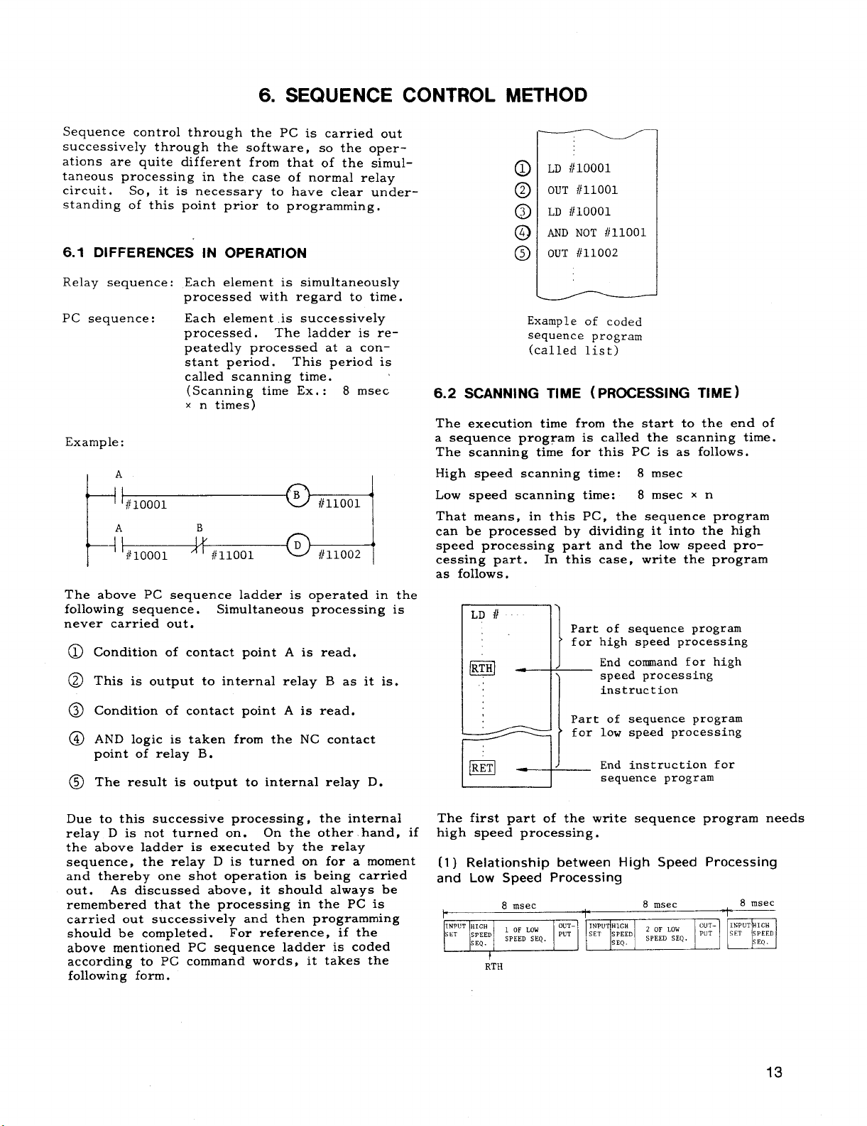
LD //10001
OUT I11OO1
LD #10001
AND NOT #11001
OUT #11002
Example of coded
sequence program
(called list)
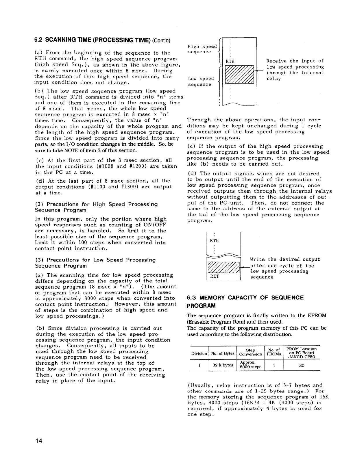
6.2 SCANNING TIME (PR~EssING TIME)
The execution time from the start to the end of
a sequence program is called the scanning time.
The scanning time for this PC is as follows.
High speed scanning time: 8 msec
Low speed scanning time: 8 msec
That means, in this PC, the sequence program
can be processed by dividing it into the high
speed processing part and the low speed processing part.
as follows.
71
@
:-IT
+!
In this case, write the program
Part of sequence program
for high speed processing
j Endcomnand forhigh
speed processing
instruct ion
Part of sequence program
for low speed processing
End instruction for
x n
E-.II#-‘equence program
Due to this successive processing, the internal
relay D is not turned on.
the above ladder is executed by the relay
sequence, the relay D is turned on for a moment
and thereby one shot operation is being carried
out .
remembered that the processing in the PC is
carried out successively and then programming
should be completed.
above mentioned PC sequence ladder is coded
according to PC command words, it takes the
As discussed above, it should always be
following form.
On the other hand, if
For reference, if the
The first part of the write sequence program needs
high speed processing. “ - -
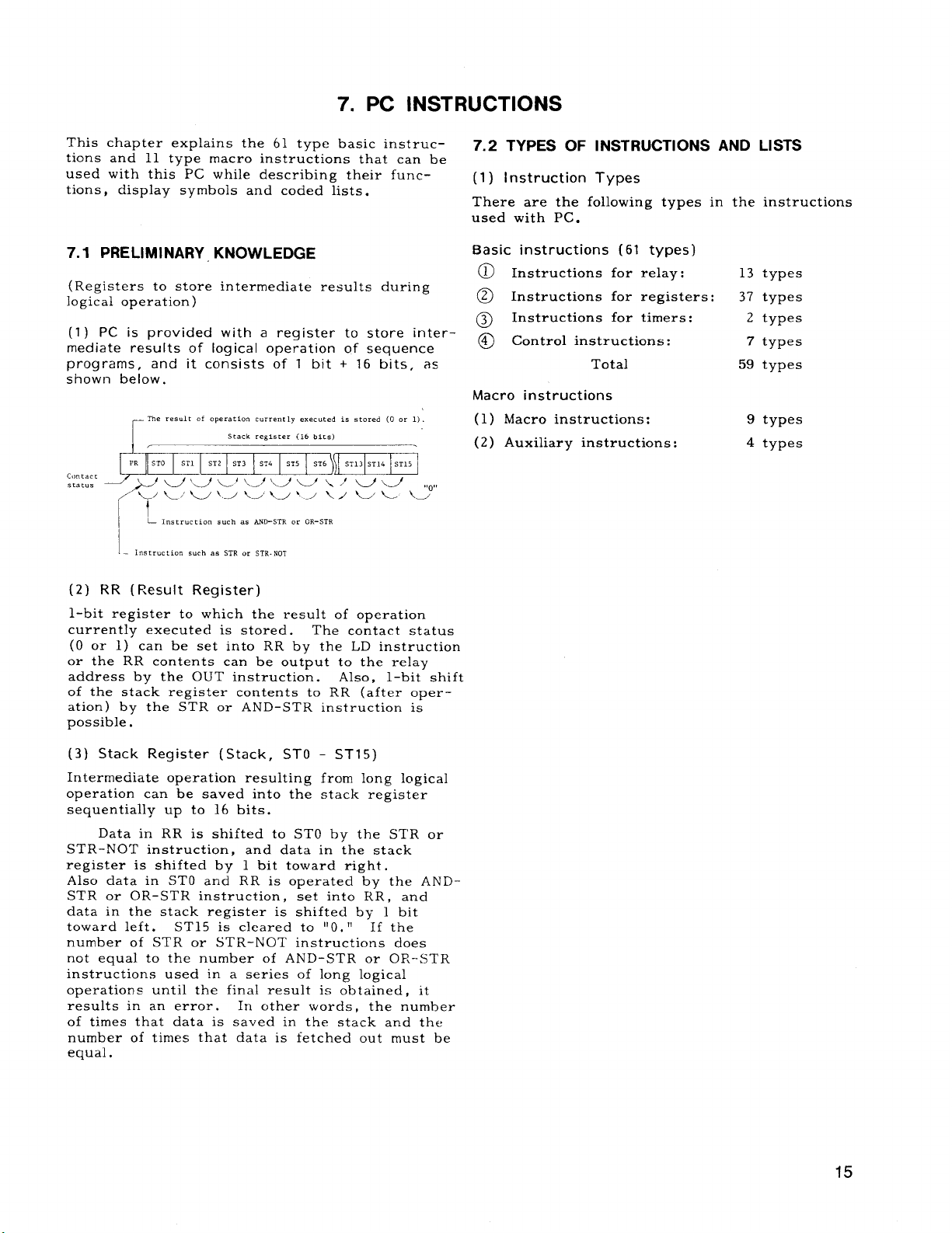
(1) Relationship between High Speed Processing
and Low Speed Processing
i-
m~=
RTH
8 msec
1-
8 msec
1-
8 msec
13
Page 18
6.2 SCANNING TIME (PROCESSING TIME) (Cent’d)
(a) From the beginning of the sequence to the
RTH command,
(high speed Seq.),
is surely executed once within 8 msec.
the execution of this high speed sequence, the
input condition does not change.
(b) The low speed sequence program (low speed
Sea.) after RTH command is divided into “n” items
and one of them is executed in the remaining time
of 8 msec.
sequence program is executed in 8 msec
times time. Consequently, the value of “n”
depends on the capacity of the whole program and
the length of the high speed sequence program.
Since the low speed program is divided into many
parts,sotheI/Oconditionchanges in the middle. So,be
sure totake NOTE ofitem3 ofthis section.
(c) At the first part of the 8 msec section, all
the input conditions (#1000 and #1200) aye taken
in the PC at a time.
(d) At the last part of 8 msec section, all the
output conditions (#1100 and #1300) are output
at a time.
(2) Precautions for High Speed Processing
Sequence Program
In this program, only the portion where high
speed responses such as counting of ON/OFF
are necessary, is handled. So limit it to the
least possible size of the sequence program.
Limit it within 100 steps when converted into
contact point instruction.
the high
That means, the whole low speed
speed sequence program
as shown in the above figure,
During
x “n”
High speed
sequence
RTH
Low speed
sequence
Through the above operations, the input conditions-may be kept ;nchanged during 1 cycle
of execution of the low speed processing
sequence program,
(c) If the output of the high speed processing
sequence program is to be used in the low speed
processing sequence program, the processing
like (b) needs to be carried out.
(d) The output signals which are not desired
to be output until the end of the execution of
low speed processing sequence program, once
received outputs them through the internal relays
without outputting them to the addresses of output of the PC unit.
same to the address of the external output at
the tail of the low speed processing sequence
program.
RTH
1’
I
Receive the input of
low speed processing
– through the internal
relay
Then, do not connect the
(3) Precautions for Low Speed Processing
Sequence Program
(a) The scanning time for low speed processing
differs depending on the capacity of the total
sequence program (8 msec
of program that can be executed within 8 msec
is approximately 3000 steps when converted into
contact point instruction.
of steps is the combination of high speed and
low speed processing. )
(b) Since division processing is carried out
during the execution of the low speed processing sequence program, the input condition
changes.
used through the low speed processing
sequence program need to be received
through the internal relays at the top of
the low speed processing sequence program.
Then, use the contact point of the receiving
relay in place of the input.
Consequently, all inputs to be
x “n”).
However, this amount
(The amount
Write the desired output
after one cycle of the
low speed processing
sequence
6.3 MEMORY CAPACITY OF SEQUENCE
PROGRAM
The sequence program is finally written to the EPROM
(Erasable Program Rem) and then used.
The capacity of the program memory of this PC can be
used according to the following distribution.
Division No. of Bytes c~nven~i~n pROMS
1 32 kbytes
(Usually, relay instruction is of 3-7 bytes and
other commands are of 1-25 bytes range. ) For
the memory storing the sequence program of 16K
bytes, 4000 steps (16 K/4 = 4K (4000 steps) is
required, if approximately 4 bytes is used for
one step.
Step
Approx.
8000steps
No.of
PROM Location
1
on
PCBoard
JANCD-CP50
30
14
Page 19
7. PC INSTRUCTIONS
This chapter explains the 61 type basic instructions and 11 type macro instructions that can be
used with this PC while describing their functions,
display symbols and coded lists.
7.1 PRELIMINARY KNOWLEDGE
(Registers to store intermediate results during
logical operation )
(1) PC is provided with a register to store intermediate results of logical operation of sequence
programs,
and it consists of 1 bit + 16 bits, as
shown below.
~-
Th. T.SU1, .f operationcurrencly executed is stored (0 or 1)
L I.str.ctIon such .S AND-STRor OR-STR
i’
[- lns,rucrfonsuch ., STR ., STR.NOT
(2) RR (Result Register)
l-bit register to which the result of operation
currently executed is stored. The contact status
(O or 1) can be set into RR by the LD instruction
or the RR contents can be output to the relay
address by the OUT instruction.
Also, l-bit shift
of the stack register contents to RR (after oper–
ation) by the STR or AN D–STR instruction is
possible.
7.2 TYPES OF INSTRUCTIONS AND LISTS
(1) Instruction Types
There are the following types in the instructions
used with PC.
Basic instructions (61 types)
@) Instructions for relay:
13 types
@ Instructions for registers: 37 types
@) Instructions for timers:
@ Control instructions:
Total
2 types
7 types
59 types
Macro instructions
(1)
Macro instructions:
(2)
Auxiliary instructions:
9 types
4 types
(3) Stack Register (Stack, STO - ST15)
Intermediate operation resulting from long logical
operation can be saved into the stack register
sequentially up to 16 bits,
Data in RR is shifted to STO by the STR or
STR-NOT instruction, and data in the stack
register is shifted by 1 bit toward right .
Also data in STO and RR is operated by the ANDSTR or OR-STR instruction, set into RR, and
data in the stack register is shifted by 1 bit
toward left. ST15 is cleared to “O. “
If the
number of STR or ST R-NOT instructions does
not equal to the number of AN D–STR or OP.-STR
instructions used in a series of long logical
operations until the final result is obtained, it
results in an error. In other words , the number
of times that data is saved in the stack and the
number of times that data is fetched out must be
equal.
15
Page 20
7.2 TYPES OF INSTRUCTIONS AND LISTS (Cent’d )
(2) List of instructions for relay
=7===
-+--b=-
+-+=
5
6
7 I XOR
8 I XNR
9
10 ST R-NOT
11 AN D-STR
12
=+=
13 I
Note:
1. The * column shows the execution time converted to the contact instruction
2, The $ mark shows that the RR contents change after instructions are operated.
OR
I
OR-NOT
I
STR
I
OR-STR
OUT
(1 = One contact instruction)
The — mark shows that no change occurs.
*
1
Reads signal status (0 or 1) and sets it to RR
I
Reads inversion signal status and sets it to RR
1
I
1 Sets
1
I
1
I
1
I
1
I
1
I
1
I
1
1
1
1
AND of contact and RR to RR (AND)
Sets AND of inversion signal and RR to RR
(Reverse AND)
Sets OR of signal and RR to RR (OR) .
Sets OR of inversion signal and RR to RR
(Reverse OR) .
Sets uncoincidence between signal and RR to RR .
Sets coincidence between signal and RR to RR.
Loads RR contents to stack and executes LD
instruction .
Loads RR contents to stack and executes LD NOT
instruction .
I
Sets AND of RR and stack to RR.
I
Sets OR of RR and stack to RR.
Writes operation results (RR) to relay (address) .
,
Meaning
RR after
operation
I 1
I
I
I 1 I
I
I
I 1 I
I I I
I
I
I
I
I 1 I
1
—
t ,
I
I
I
I
I
I
I
Page
19
19
20
20
20
20
20
20
21
21
21
21
21
(3) List of Instructions for Timers
Instruction * Meaning
No.
10 Timer processing (Fixed timer)
10
Timer processing (Variable timer)
16
1
2
TIM
TlvfR
RR after
operation
time up = 1 22
time up = 1 22
Page
Page 21
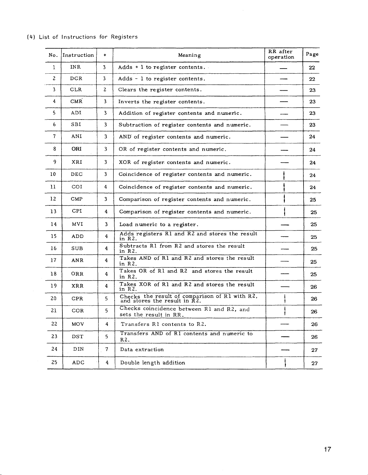
(4) List of Instructions for Registers
No. Instruction *
IN R
1
I
DCR
21
CLR \ 2 I Clears the register contents.
31
CMR I 3 I Inverts the register contents.
41
51
61
71
10 DEC 3 Coincidence of register contents and numeric.
11
12
13
14
15 ADD 4
16
17 AN R
18
19 XRR
20
21
22 I MOV
23 DST
24 I
ADI
SBI
‘N’ I 3 IANISO
8 OR1
9
XRI
COI
I
CMP
I
CPI
I
MVI
SUB
I
ORR
1 I 1
CPR
COR
DIN 1, 7 I Data extraction
I
Adds + 1 to register contents.
3
I
I
I 3 I Adds -1 to register contents.
I 3 I Addition of register contents and numeric.
] 3 I Subtraction of register contents and numeric. I –
f register contents and numeric,
3 OR of register contents and numeric.
3 XOR of register. contents and numeric.
4
I
I
I
I
[ ,
I 4 I Transfers R1 contents to R2.
I
Coincidence of register contents and numeric.
I
3IComparison of register contents and numeric.
4IComparison of register contents and numeric.
3 Load numeric to a register.
Adds registers R1 and R2 and stores the result
in R2.
Subtracts R1 from R2 and stores the result
4
in R2.
I
Takes AND of R1 and R2 and stores the result
4
in R2.
Takes OR of R1 and R2 and stores the result
4
in R2.
Takes XOR of R1 and R2 and stores the result
4
in R2.
Checks
5
I and stores the result in I?2.
Checks coincidence between R1 and R2, and
5
sets the result in RR.
Transfers AND of R1 contents and numeric to
5
R2.
the result of com arisen of R1 with R2,
Meaning
RR after
oDeration
I
—
I
l–
I –
l–
l–
I – H“
—
—
1
I 1
I
I
I
1
I
—
—
—
—
—
—
I
Page
22
I
I 22
123
I 23
I 23
I 23
24
24
24
24
I
25
I
I
I
t
25
2!5
25
25
25
26
I
I
l—
I
—
–127
I 26
25
26
26
26
25
ADC
I
4IDouble length addition
I
17
Page 22

7.2 TYPES OF INSTRUCTIONS AND LISTS ( Cent’d )
No.
:nstructio]
26
27
28
29
30 lNRW
31
32
34
35
36
37
ADDW
SUBW
MULW
DIVW
DCRW
CLRW
CORW
CPRW
MVIW
DSTW
*
Adds double length registers (wR2 and WR1) and
4
stores the result in WR2.
Subtracts WR1 from WR2 and stores the result in
4
WR2,
Multiplies double length register (WR2) with regis-
10
ter (Rl) and stores the result in WR2.
Divides double length re ister (WR2) by register
15
(Rl) and stores the resu t in WR2.
3 I Adds + 1 to double length register contents.
Adds - 1 to double length register contents.
3
Clears double length register contents.
3
233 CMRW
Inverts double length register contents.
1
Sets coincidence result of double length registers
3
(WR2 and WR1) to RR.
Sets comparison result of double length registers
3
(WR2 and WR1) to RR.
Loads numeric to double length register.
3
Transfers AND of double length register (WR1)
5
contents and numeric to doub–le len~th register
(WR2) .
Meaning
?
RR after
operation
H-
1s set to
RR “
“ 1“ when
overflow occurs.
*
—
I
—
1
I
I
I
1
I
Page
I
I
I
129
27
28
29
29
29
29
29
29
30
(5) List of Control Instructions
No. nstruction
1
2
3
4
5
6
7
NOP
MCR I 1 I Start of master control relay.
END 1
RET
RTI
SET
RTH
*
1 No-operation.
1 I
1 I Sequence program termination.
r m is set tO
1
I
1
1
‘-””1”
Meaning
End of master control relay.
and RET instruction is executed.
“ 1”
Sets RR to “ 1. “
High speed processing sequence program
termination.
RR after
operation
.—
1
Page
30
30
30
30
30
31
31
Page 23
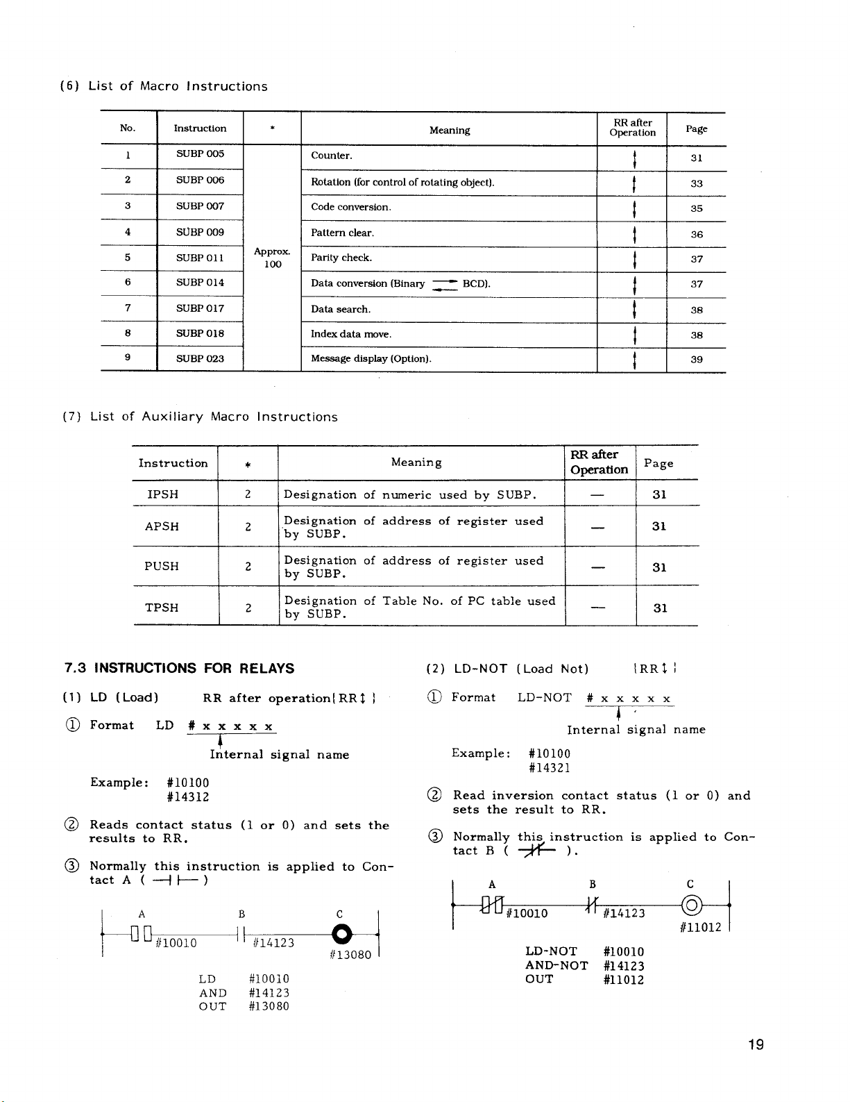
(6) List of Macro Instructions
No.
1
2
3
4
5
6
7
6
9
(7) List of Auxiliary Macro Instructions
Instruction
SUBP005
SUBP006
SU13P007 Codeconversion.
S~BP009
SUBP011
SUBP014 Dataconversion(Bina~
SUBP017 Datasearch.
SUBP018 Indexdatamove.
SUBP023
Instruction
IPSH
APSH
PUSH
I I
I
I
*
Approx.
100
*
Designation of numeric used by SUBP.
2
Designation of address of register used
2
“by SUBP.
Designation of address of register used
2
by SUBP.
Meaning
Counter.
Rotation(forcontrolofrotatingobject).
Patternclear.
Parttycheck.
— BCD).
MeaSagedispfay(Option).
Meaning
RR after
Operation
—
I
—
I
—
I
RRafter
Operation
1
1
1
1
1
t
1
1
I
‘age
[
I
I
Page
31
33
35
36
37
37
38
38
39
31
31
31
TPSH
7,3 INSTRUCTIONS FOR RELAYS
LD ( Load)
Format
Example:
Reads contact status ( 1 or O) and sets the
results to RR.
Normally this instruction is applied to Contact
LD#xx xxx
#loloo
#14312
I
RR after operation{ RR $ I
!
Internal signal name
LD
AND
OUT
Designation of Table No. of PC table used _
2
by SUBP.
#loolo
#14123
#13080
31
I
4
1 #14123
#loolo
#llo12
IRRI }
,
c
& ‘
{/11012
LD-NOT (Load Not)
Format
Example:
Read inversion contact status ( 1 or O) and
sets the result to RR.
Normally this instruction is applied to Contact B ( ~Y~ ) .
+/}10010
LD-NOT#xx xxx
Internal signal name
#loloo
#14321
A
LD-NOT
AND-NOT #14123
OUT
B
1/
4
19
Page 24
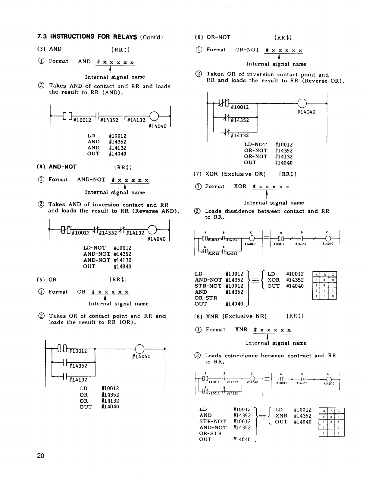
7.3 INSTRUCTIONS FOR RELAYS (Cent’d )
(6)
OR-NOT
[RR$)
(3) AND
@ Format
@ Takes AND of contact and
the result to RR (AND).
(4) AND-NOT
@ Format
@) Takes AND of inversion contact and RR
and loads the result to RR (Reverse AND).
AND#x xxx
Internal signal
LD
AND
AND
OUT
AND-NOT # X X X X X
Internal signal name
{RR$I
+
#loo12
#14352
#14132
#14040
{RR$ ]
x
—
name
RR and loads
+
@ Format
@ Taken OR of inversion contact point and
RR and loads the result to RR (Reverse OR).
1’4;
(7) X(3R (Exclusive OR)
@ Format
@ Loads dissidence between contact and RR
to RR.
OR-NOT #xx xxx
Internal signal name
1
#14132
HI-NOT #10012
OR-NOT #14352
OR-NOT #14132
OUT
XOR#xx xxx
Internal signal name
t
#14040
t
{RR$j
lx lx
=Qfkoolz ‘1
(5) OR
@ Format
@ Takes OR of contact point and RR and
loads the result to Rk (OR).
E“”””
I
OR#xx xxx
#14352
#14132
I#14352 ~ t //14132
LD-NOT #10012
AND-NOT #14352
AND-NOT #14132
OUT
Internal signal name
!
#1
{RR1}
4040
~
LD
OR
OR
OUT #14040
#loo12
#14352
#14132
{/14040
#14040
0’
‘
I
XNR (Exclusive NR)
(8)
@ Format
@ Loads coincidence between contract and RR
—
to RR.
XNR#xx xxx
Internal signal name
4
{RR$}
20
Page 25
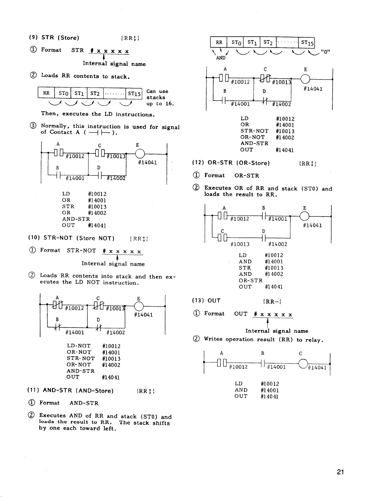
(9) STR (Store)
{RR$I
@ Format
@ Loads RR contents to stack.
RR
Utitiu u
Then, executes the LD instructions.
@ Normally, this instruction is used for signal
of Contact A ( ~ ~ ) .
1A
STR#xx xxx
Internal signal name
STO ST1
LD
OR
STR
OR
AND-STR
OUT
#loo12
#14001
#loo13
#14002
#14041
ST.2 .. . . .... ST15 ~aC;e
Up to 16.
c
E
I
1A
tl+~
II
(12) OR-STR (OR-Store)
Format
Executes OR of RR and stack (STO ) and
loads the result to RR.
/)10012 ] Jm/loo131
B
41
/)14001
LD
OR
STR-NOT #10013
OR-NOT
AND-STR
OUT
OR-STR
1A
{/19012
t---F’
c
I
ID
1
I,k’
41
#14002
#loo12
#14001
#14002
#14041
B E
‘-
I
I
{RR$;
E
#14041
1
I
I
(10) STR-NOT (Store NOT)
Format ST R-NOT # x x x x x
Internal signal name
Loads RR contents into stack and
ecutes the LD NOT instruction.
A
,
- #loo12 B
1>
L
/)14001
LD-NOT
OR-NOT
STR-NOT #10013
OR- NOT
AND-STR
OUT
) AND-STR (AND-Store)
Format
Executes AND of RR and stack (STO ) and
loads the result to RR.
by one each toward left.
AND-STR
c
{/10013’
D
1
II
’11
#14002
#loo12
#14001
#14002
#14041
{RR~;
E
{/14041
J
{RR$!
The stack shifts
then ex-
4I
I
I4h----iJl----J
(13) OUT
@ Format
@ Writes operation result (RR) to relay.
#loo13
LD
AND
STR
AND
OR-STR
OUT
OUT#xx xxx
Internal signal name
LD
AND
OUT
#14002
#loo12
#14001
#loo13
#14002
#14041
{RR–I
t
#loo12
#14001
#14041
21
Page 26
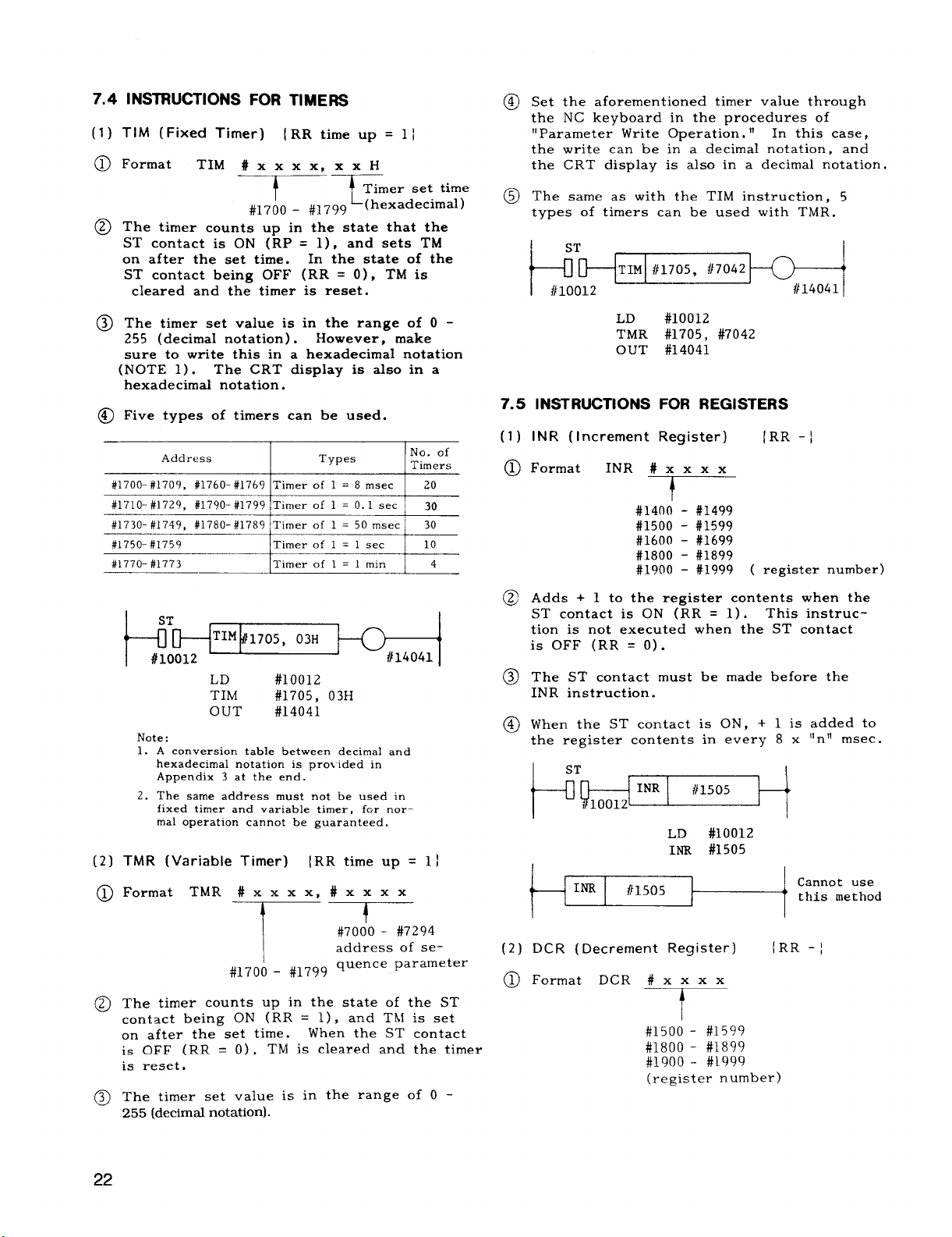
7.4 INSTRUCTIONS FOR TIMERS
(1) TIM
@ Format
(Fixed Timer) {RR time up = 1}
TIM#xxxx, xxH
Set the aforementioned timer value through
the NC keyboard in the procedures of
“Parameter Write Operation. “ In this case,
the write can be in a decimal notation, and
the CRT display is also in a decimal notation.
‘~~;::::::;
#1700 - #1799
@ The timer counts up in the state that the
ST contact is ON (RP = 1), and sets TM
on after the set time.
In the state of the
ST contact being OFF (RR = O), TM is
cleared and the timer is reset.
@) The timer set value is in the range of O -
255 (decimal notation). However, make
sure to write this in a hexadecimal notation
(NOTE 1).
The CRT display is also in a
hexadecimal notation.
@ Five types of timers can be used.
Address
#1700-#1709, #1760-#1769 Timer of 1 = 8 msec
#1710-#1729. #1790-#1799 \Timer of 1 = 0.1 sec / 30
#1730-#1749, #1780-#1789 \Timer of 1 = 50 msec \ 30
#1750-#1759
#1770-#1773 Timer of 1 = 1 min
I
Types
Timer of 1 = 1 sec 10
No. of
Timers
20
I
4
ST
TIM }1705, (J3H
#loo12
t+ ‘~ ~
LD
TIM
OUT
Note:
1. A conversion
hexadecimal notation is pro~ ided in
Appendix 3 at the end.
2. The same address must not be used in
fixed timer and variable timer, for nor-
mal operation cannot be guaranteed.
#loo12
#1705, 03H
#14041
table between decimal and
#14041
TMR (Variable Timer) {RR time up = 1 \
Format TMR#xxxx, # xxxx
~ T—
#7000 - #7294
1
#170A - #1799 q
address of se-
uence parameter
The timer counts up in the state of the ST
contact being ON (RR = 1) , and TM is set
on after the set time.
When the ST contact
is OFF (RR = O) , TM is cleared and the timer
is reset.
The timer set value
is in the range of O -
255 (decimal notation).
The same as with the TIM instruction, 5
types of timers can be used with TMR.
I
ST
TIM #1705, #7042
//10012
t+ 1
7.5 INSTRUCTIONS
(1)
INR (Increment
LD
TMR
OUT
#loo12
#1705, #7042
#14041
FOR REGISTERS
Register) {RR -j
Format INR#x xxx
#1400 - #1499
#1500 - #1599
#1600 - #1699
#1800 - #1899
regkter number)
Adds + 1
#1900 - #1999 (
to the register contents when the
ST contact is ON (RR = 1). This instruction is not executed when the ST contact
is OFF (RR = O).
The ST contact must be made before the
INR instruction.
the ST contact is ON, + 1 is added to
When
the register contents in every 8 x “n” msec.
ST
INR
#1505
LD #10012
INR #1505
Cannot use
(,
this method
DCR (Decrement Register)
Format DCR # x x x x
4
{RR -~
I
#1500 - #1599
#1800 - #1899
#1900 - #1999
(register number)
4I
Page 27
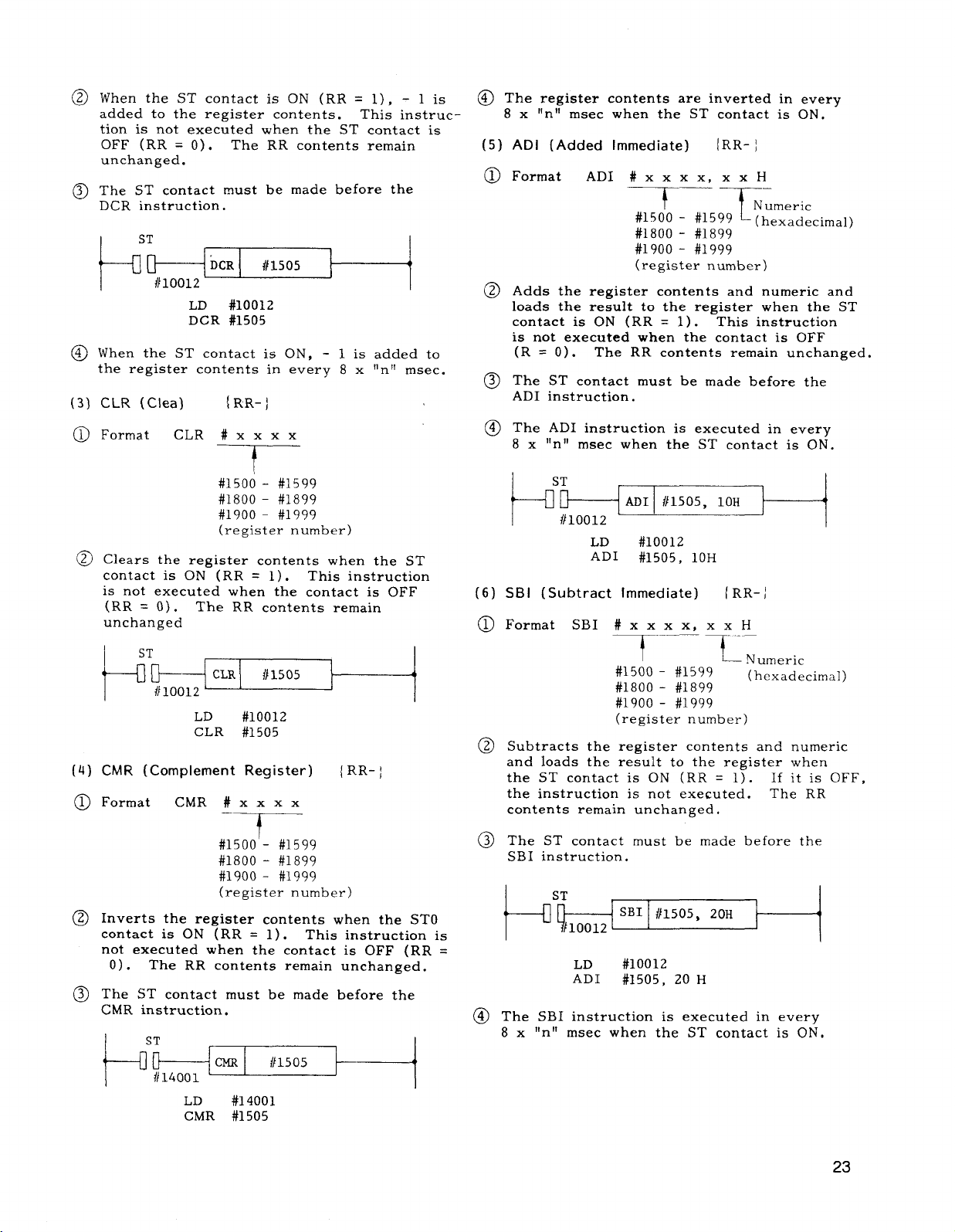
.... ..n -
when the S1’ contact is
added to the register contents.
tion is not executed when the ST contact is
OFF (RR = o). The RR contents remain
unchanged.
The ST contact must be made before the
DCR instruction.
ST
DCR
b~ ‘-
When the ST contact is ON, - 1 is added to
the register contents in every 8 x ‘In!! msec.
CLR (Clea)
Format
Clears the register contents when the ST
contact is ON (RR = 1). This instruction
is not executed when the contact is OFF
(RR =
unchanged
//10012
LD #10012
DCR #1505
{RR-j
CLR#x xxx
#1500 - #1599
#1800 - #1899
#1900 - #1999
(register number)
o).
The RR contents remain
LD
CLR #1505
#loo12
CMR (Complement Register)
Format
Inverts the register contents when the STO
contact is ON (RR = 1) . This instruction is
not executed when the contact is OFF (RR =
o). The RR contents remain unchanged.
The ST contact must be made before the
CMR instruction.
P+ml
CMR#x xxx
ST
//14001
LD
CMR #1505
‘7
#1500 - #1599
#1800 - #1899
#1900 - #1999
(register number)
#14001
-.. ,—-. .
UN (KK = 1) , - 1 is
#1505
!
{RR-~
#1505
+--i
This instruc-
<1
@ The register contents are inverted in everv
8 x “n’~ msec when the ST contact is ON. ‘
AD I (Added Immediate)
Format ADI#xxxx, xxH
X5~;meric
#1800 - #1899
#1900 - #1999
(register number)
Adds the register contents and numeric and
loads the result to the register when the ST
contact is ON (RR = 1) . This instruction
is not executed when the contact is OFF
(R= O). The RR contents remain unchanged.
The ST contact must be made before the
AD I instruction.
The ADI instruction is executed in every
8 x “n” msec when the ST contact is ON.
ST
ADI #1505, 10H
1- ~f
SBI (Subtract Immediate)
Format SBI#xxxx, xx H
Subtracts the register contents and numeric
and loads the result to the register when
the ST contact is ON (RR = 1) . If it is OFF,
the instruction is not executed.
contents remain unchanged.
The ST contact must be made before the
SBI instruction.
t-+---+ 1-1
rhe SBI instruction is executed in every
) x “n” msec when the ST contact is ON,
#loo12
LD
AD1 #1505, 10H
_l–.-—
#1500 - #1599
#1800 - #1899
#1900 - #1999
(register number)
ST
)10012
AD I
SB1 #1505, 20H
LD
#loo12
#1505, 20 H
#loo12
1
{RR-;
(hexadecimal)
( RR-;
~...-
L ~umeric
(hexadecimal)
The RR
~
A
I
23
Page 28
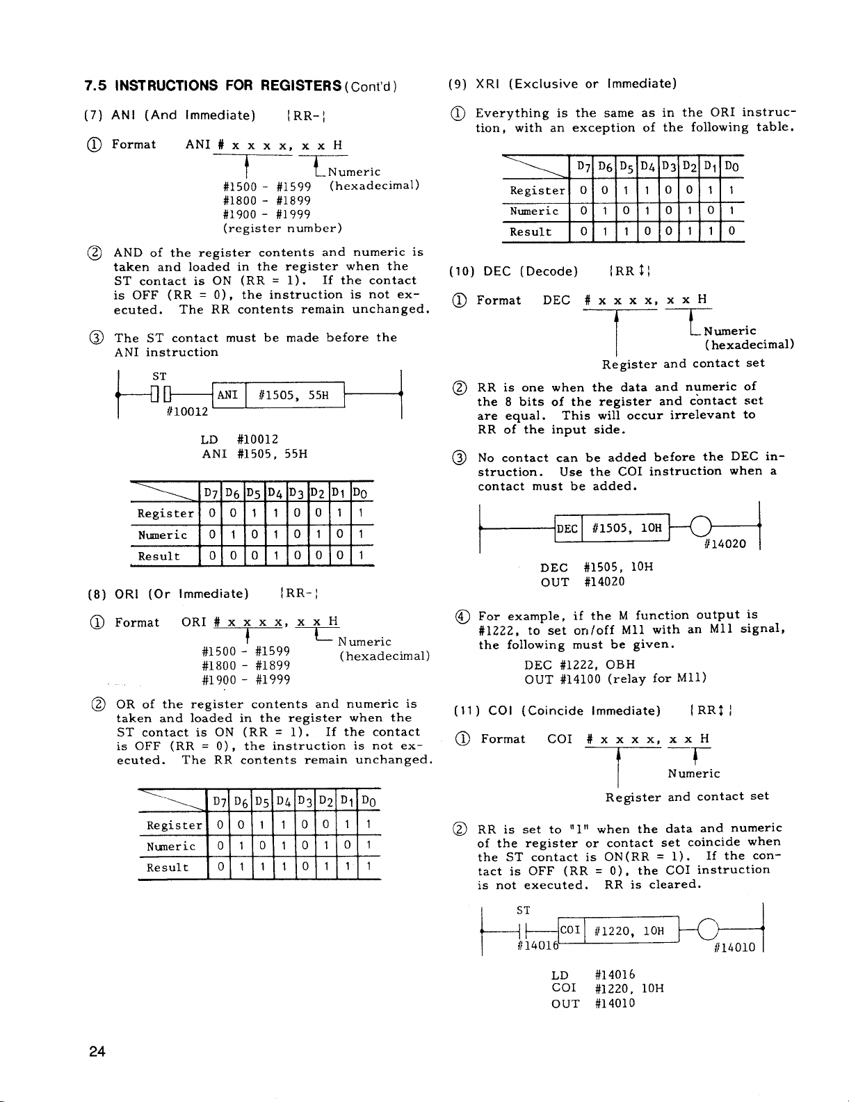
7.5 INSTRUCTIONS FOR REGISTERS
Cent’d )
(9)
XRI (Exclusive or Immediate)
AN I (And Immediate)
Format
ANI#xxxx, xxH
— —
t
#1500 - #1599 (hexadecimal)
#1800 - #1899
#1900 - #1999
(register number)
of the register contents and numeric is
AND
taken and load~d in the register when the
ST contact is ON (RR = 1). If the contact
is OFF (RR = O) , the instruction is not ex-
ecuted.
The ST contact must be made before the
ANI instruction
t----- 1
Re~ister o 0 1
Numeric 1011 !01110111011
Result
ORI
Format
The RR contents remain unchanged.
ST
WI
#loo12
LD #10012
ANI #1505, 55H
D7 D6 D5 n). ln~ ln~ Inf Inn
0 001 0 O1o11
I
(Or Immediate)
ORI#xxxx, xxH
——
1
#1500 - #1599
#1800 - #1899
{RR-]
L. umeric
/}1505, 55H
t
tmT-tw-
IRR-1
!-
Numeric
(hexadecimal)
#1900 “ #1999
OR of the register contents and numeric is
taken and loaded in the register when the
ST contact is ON (RR = 1). If the contact
is OFF (RR = O) , the instruction is not ex–
ecuted.
-..
The RR contents remain unchanged.
‘.
D7 D6 D5
D4 D3 D2
D1 D()
@ Everything is the same as in the ORI instruc-
tion, with an exception of the following table.
D7 D6 D5 D4 D3 D2
Register o 0 1 1 0 0 1 1
Numeric o 1 0 1 0 1 0 1
Result o 1
(10) DEC (Decode)
Format
d1
RR is one when the data and numeric of
the 8 bits of the register and contact set
are equal.
RR of the input side.
No contact can be added before the DEC instruction.
contact must be added.
For example, if the M function output is
#1222, to set on/off Mll with an Mll signal,
the following must be given.
(11 ) CO I (Coincide Immediate) {RR$ ~
@ Format
DEC#xxxx, xxH
This will occur irrelevant to
Use the COI instruction when a
DEC #1505, 10H
OUT #14020
DEC #1222, OBH
OUT #14100 (relay for Mll)
COI#xxxx, xxH
1 0 0 1 1 0
[RR$;
T~:::::cimal)
Register and contact set
T
Register and contact set
D1 DO
‘r
Numeric
24
Register o 0 1
Nuneric
Result
o 1 0
o 1 1 1 0 1 1 1
1 0 0 1 1
1 0 1
0 1
@ RR is set to
of the register or contact set coincide when
the ST contact is ON(RR = 1). If the contact is OFF (RR = O) , the COI instruction
is not executed.
It111when the data and numeric
RR is cleared.
t--i--,+=l=l=l
LD #14016
COI
OUT #14010
#1220, 10H
Page 29
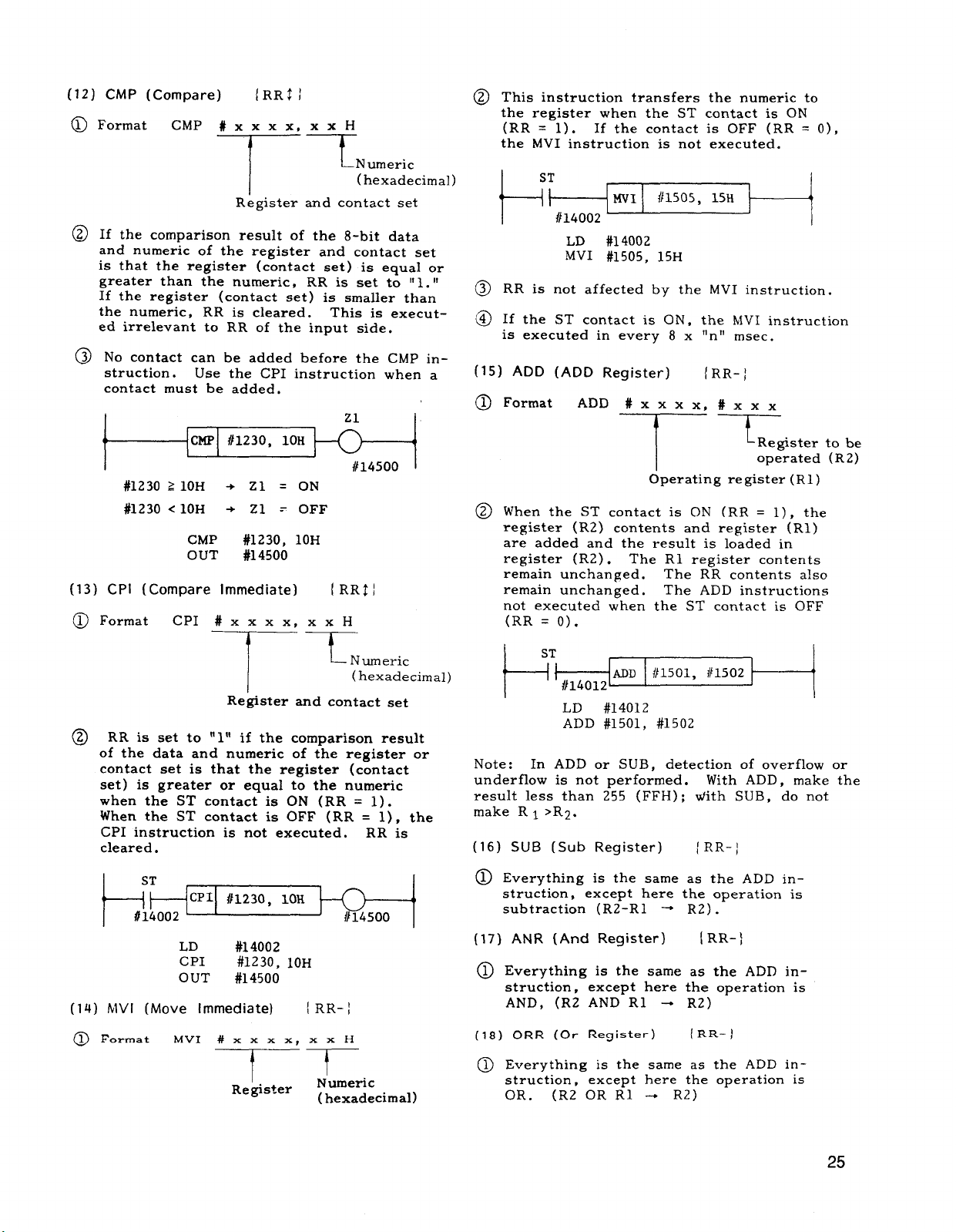
(12) CMP (Compare)
Format
If the comparison result of the 8-bit data
and numeric of the register and contact set
is that the register (contact set) is equal or
greater than the numeric, RR is set to “1.1’
If the register (contact set) is smaller than
the numeric, RR is cleared. This is executed irrelevant to RR of the input side.
No contact can be added before the CMP instruction.
contact must be added.
CMP
Use the CPI instruction when a
cm
I
#1230 2 10H
#1230 < 10H
CMP
OUT
CPI (Compare Immediate)
(13)
Format
CPI#xxxx, xxH
{RR$;
#xx XX, XXH
——
L
Numeric
!
Register and contact set
#1230, 10H
~Zl=ON
~ 21 = OFF
#1230, 10H
#14500
(hexadecimal)
Z1
#14500 I
{RR$I
This instruction transfers the numeric to
@
the register when the ST contact is ON
(RR = 1). If the contact is OFF (RR = O),
the MVI instruction is not executed.
ST
MVI #1505, 15H
k~~
RR is not affected by the MVI instruction.
@
If the ST contact is ON, the MV1 instruction
CD
is executed in every 8 x “n” msec.
(15)
Format
When the ST contact is ON (RR = 1) , the
register (R2) contents and register (Rl)
are added and the result is loaded in
register (R2) .
remain unchanged. The RR contents also
remain unchanged. The ADD instructions
not executed when the ST contact is OFF
(RR = o).
#14002
LD #14002
MVI #1505, 15H
ADD (ADD Register)
ADD#xxxx, #xxx
T
The R1 register contents
RR-;
{
~ti5ter
operated
Operating register (Rl )
4
to be
(R2)
T
Numeric
T“
Register and contact set
RR is set to “ 1“ if the comparison result
of the data and numeric of the register or
contact set is that the register (contact
set ) is greater or equal to the numeric
when the ST contact is ON (RR = 1).
When the ST contact is OFF (RR = 1) , the
CPI instruction is not executed. RR is
cleared.
(hexadecimal])
t-+~~-=---l
LD
CPI
OUT
(14) MVI (Move Immediate)
Format
@
h4VI#Xxxx, xxH
#14002
#1230, 10H
#14500
——
I
Register
{ RR- )
!
Numeric
(hexadecimal)
ST
b}+ ‘-
Note:
underflow is not performed.
result less than 255 (FFH) ; With SUB, do not
make R 1 >R2.
(16) SUB (Sub Register)
@ Everything is the same as the ADD in-
struction,
subtraction (R2-R1 - R2) .
(17) ANR (And
@ Everything is the same as the ADI) in-
struction,
AND, (RZ AND R1 ~ R2)
(18) ORR (Or Register)
@ Everything is the same
struction,
OR. (R2 OR R1 -+ R2)
#14012
LD #14012
ADD #1501, #1502
In ADD or SUB, detection of overflow or
ADD #1501, {/1502
With ADD, make the
[ RR-j
except here the operation is
(
Register)
except here the operation is
except here the operation is
RR-)
( RR- )
as the ADD in-
a
25
Page 30
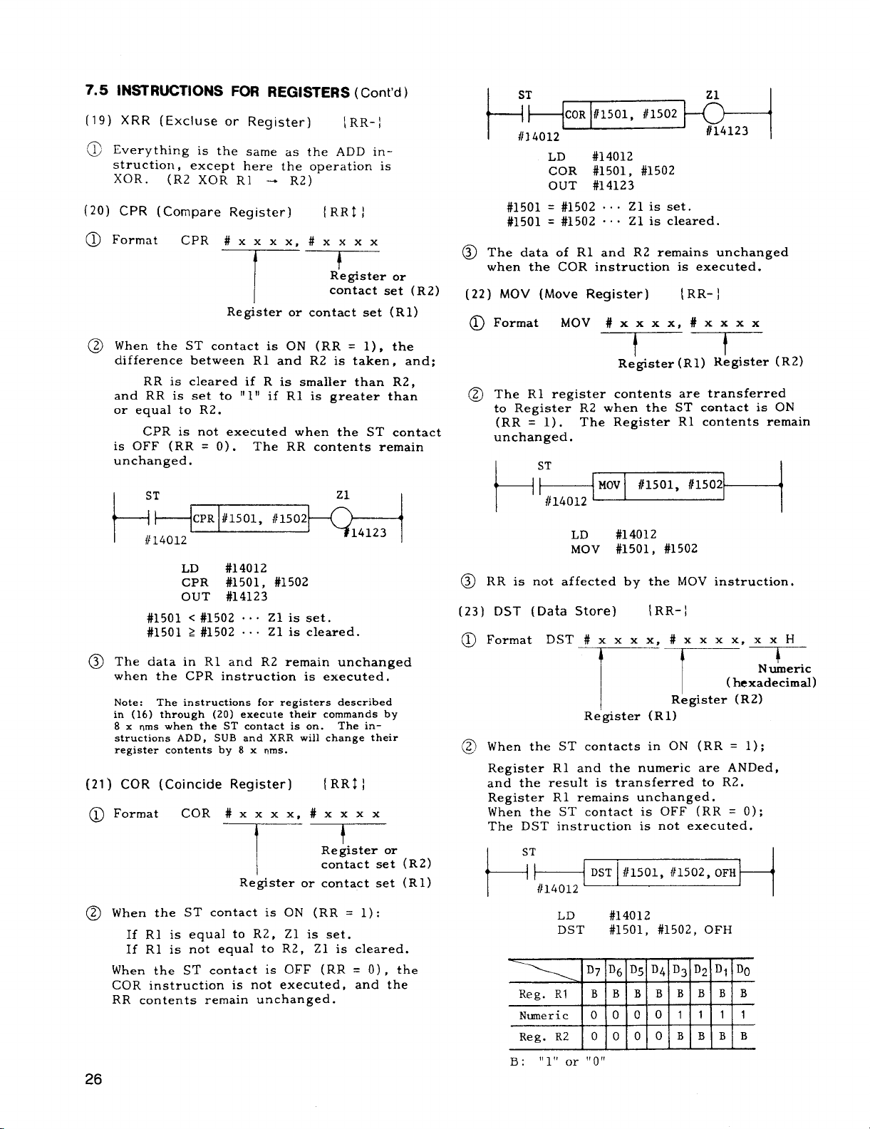
7.5 INSTRUCTIONS FOR REGISTERS ( Cent’d )
(19) XRR (Excluse or Register)
@ Everything is the same as the ADD in-
struction,
XOR.
(20) CPR (Compare Register)
@ Format
@ When the ST contact is ON (RR = 1), the
difference between R1 and R2 is taken, and;
RR is cleared if R is smaller than R2,
and RR is set to “ 1“ if R1 is greater than
or equal to R2.
CPR is not executed when the ST contact
is OFF (RR = O).
unchanged.
ST
l++ I
I
#14012
#1501 c #1502 0.. 21 is set.
#1501 2 #1502 . . . 21 is cleared.
@) The
when the CPR instruction is executed,
Note: The instructions for registers described
in ( 16) through (20) execute their commands by
8 x nms when the ST contact is on. The instructions ADD, SUB and XRR will change their
register contents by 8 x rims.
(21 ) COR (Coincide Register)
@ Format
@ When the ST contact is ON (RR = 1):
If RI is equal to R2, Z1 is set.
If R1 is not equal to R2, Z1 is
When the ST contact is OFF (RR
COR instruction is not executed,
RR contents remain unchanged.
except here the operation is
(R2 XOR RI -+ R2)
CPR#xxxx, #x xxx
T’
Register or contact set (R 1)
The RR contents remain
CPR #1501, #1502
LD
CPR #1501, #1502
OUT #14123
data in R1 and R2 remain unchanged
COR#xxxx, #x xxx
#14012
T’
Register or contact set (R 1)
{RR- I
{RR$j
Register or
contact set (R2)
Z1
{RRI]
Register or
contact set (R2)
cleared.
= O), the
and the
26
ST Z1
COR #1501, #1502
t+ 1
#14012
LD #14012
COR #1501, #1502
OUT #14123
#1501 = #1502 ,.. 21 is set.
#1501 = #1502 . ““ Z1 is cleared.
@) The data of R1 and R2 remains unchanged
when the COR instruction is executed. -
{RR- I
{RR-)
D2 D1 DO
B B B
1 1 1
, I
(R2)
4I
(22) MOV
@ Format
@ The R1 register contents are transferred
to Register R2 when the ST contact is ON
(RR = 1).
unchanged.
I
I
r’
@ RR is not affected by the MOV instruction.
(23) DST (Data Store)
@Format DST#xxxx, #xxx x,xx H
@ When the ST contacts in ON (RR = 1);
Register R1 and the numeric are ANDed,
an~ the result is transferred to R2,
Register R1 remains unchanged.
When the ST contact is OFF (RR = O);
The DST instruction is not executed.
P’11
(Move Register)
MOV#xxxx, #x xxx
77
Register (Rl) Register
The Register R1 contents remain
~T I
-.
MOV #1501, #1502
#14012
LD
MOV #1501, #1502
ST
#14012
LD
DST
Reg. RI B B B B B
Numeric
Reg. R2
l!~!t or !!0!!
B:
#14012
~“G,*)
Register (Rl)
DST #1501, //1502, OFH
#14012
#1501, #1502, OFH
D6 D5 D4 D3
DT
o 0 c o 1
o 0 0 0 B B B B
Page 31

@ RR is not affected by execution of the DST
instruction.
,
I
#1503
#1502
(24] DIN (Data Insert) { RR-~
Format DIN#xxxx, # XX XX, XXH
7 T-– T
Register or
contact set (R2)
Register or contact set (Rl)
When the ST contact is ON (RR = 1) , the
R1 data and numeric are ANDed and the
result is ORed with the AND of the R2 data
and the numeric complement.
stored in R2 (data extraction) .
ST contact is OFF (RR = 1) , the DIN in-’
struction is not executed.
LD
DIN
RI AA
R2BB
n
Result B B
4
A, B:
ADC (Add with Carry)
(25)
#14012
#1501, #1502, OFH
ID71D61D51D41D31D21D11D0
A A
00
Data is “1” or “O. “
I
The result is
When the
AAA
BBB
T
—
1 11
1
AAA
A
BE
—
{RR)
Numeric
(hexadecimal)
CzEicl P=l
PR
❑
@ RR must be cleared to execute the ADC in-
struction.
(26) ADDW (Add Word Register)
@ Format
@ When the ST contact is ON (RR = 1), the
contents of double length registers, WR2
and WR1, are added and the result is
stored in WR2. WR1 remains unchanged.
(WR2) + (WR1) + (WR2) . The RR contents
do not change by the operation. When the
ST contact is OFF (RR = O) , the ADDW instruction is not executed.
is judged without code.
l+’
ADD#xxxx, #xxx x,
T’
Low side of double length
register (WR1)
ST
#14012
LD
ADDW #1500, #1502
#14012
{ RR- !
Low side of
double length
register (WR2)
The numeric
)
@ Format
@ Register Rl,
result stored in Register R2,
to “1” when a carry occurs .
l---m-+
I’1OO12
LD NOT
ADC
ADC
ADC#xxxx, #x xxx
T
Register or contact set (Rl)
R2 and RR are added, and the
ADc ;1501, #1502
#loo12
#1501, #1502
#1500, #1503
T
Register or
contact set (R2)
RR is set
ADC tlsoo,#1503
+1
(wR2)
#1503 [ #1502
(WR1)
#1501 :
r
(WR2)
I
#1500
27
Page 32

7.5 INSTRUCTIONS FOR REGISTERS (Cent’d )
(27) SUBW (Sub Word Register)
Format
SUBW
#xxx x,#x xxx
[RR-;
ST
1+--+.L
{/14012 1+
MULW //1500, {/1502
LD
#14012
MUL #1500, #1502
Low” side of
double length
register (WR2)
Low’ side of double
length register (WR1)
When the ST contact is ON (RR = 1), the
results of the contents of double length
registers, WR2 minus WR1 is stored ~n
WR2. WR1 remains unchanged.
(WR2) - (WR1) +
When the ST contact is OFF (RR = O) , the
SUBW instruction is not executed.
numeric is judged without code.
ST
SUBW
#14012
l----’+ 1~
LD
INRW #1500, #1502
#1503 : #1502
[
-)
#1501 i
[
I #15o3 ~ #1502 I
(WR2)
The
#1500, #1502
#14012
(WR2)
1
(WR1)
#1500
(WR2)
~
(RI)
‘)
#1503 : #1502
L
(29) DIVW (Division Word Register)
@ Format
@ When the ST contact is ON (RR = 1), the
contents of double length register WR2
is divided by register R1 and the result
is stored in WR2.
When the ST contact is OFF (RR = O), DIV
instruction is not executed.
is judged without code.
operation will not be executed.
DIVW#xxxx, #x xxx
TT
Regis~er (Rl)
m
(WR2)
( RR- ;
Low side of
I
WR1 remains unchanged.
double length
register (WR 2)
The numeric
If WR1 is 110,11
(WR2)
(28) MULW (Mul Word Register)
Format
When the ST contact is ON (RR = 1), the
contents of double length register, WR2
and register R1 are multiplied, and the
result is stored in WR2.
unchanged.
(WR2) x (Rl) +
When the ST contact is OFF (RR = O) , the
MUL instruction is not executed. The
numeric is judged without code.
result is overflown, more than “FFFFH ,“
RR equals one.
MULW#xxxx, #xxx
I
Register (RI)
I
(WR2)
{RRII
Low side of
double length
register (WR2)
R1 remains
If the
ST
DNW
I--+11
#14012
X
LD
DIV #1500, #1502
#1503 : #1502
‘)
#1503 !
#1500, {/1502
#14012
(WR2)
E!iIEl
#1502
(WR2)
l-+
I
(Rl)
I
Page 33

(so) INRW ( Increment Word Register)
@ Format
@ When the ST contact is ON, +1 is added to
the double length register contents.
b’
INRW#x xxx
ST
#14012
LD #14012
INRW #1500
t
I
Low’ side of double length
register
INRW
#1500
{RR- I
@ The data of WR1 and WR2 do not change
when the CORW instruction is sxecuted.
(35) CPRW (Compare Word Register) (RR$ I
@ Format CPRW#xxxx, #xxx
Double Ien gth
T’
Double length register
(WR1)
@ When the ST contact is ON (RR = 1), WR1
and WR2 are checked for the difference;
If WR1 is smaller than WR2, RR is cleared.
If WR1 is greater than or equal to WR2,
RR is set.
register (WR2)
X
(31) DCRW (Decrement Word Register) {RR-I
@ Thesame as INRW, butthe operation here
is addition of -1 to the double length
register contents.
{
(32) CLRW (Clear Word Register)
~ Thesame as INRW, buthere the double
length register contents are cleared.
(33) CMRW (Complement Word Register) {RR- I
@ The same as INRW, but here the double
length register contents are inverted.
(34) CORW (Coincide Word Register) {RR$j
@ Format
@ When the ST contact is ON (RR = 1), WRI
and WR2 are checked for the coincidence;
If WR1 and WR2 are equal, RR is set to
If WR1 and WR2 are not equal, RR is
cleared.
When the ST contact is OFF (RR = O) , the
CORW instruction is not executed, and the
RR contents remain unchanged.
b~l=’
#1500
#1500 = #1502 . . . Z1 is cleared.
CORW#xxxx, #x xxx
T-
Double length register
(WR1)
ST
CORW1/1500, #1502
#14012
LD
CORW #1500, #1502
OUT
4114012
#14123
❑ #1502 . . . Zl is set.
RR-~
F
Double length
register (WR2)
Z1
{i14123
When the ST contact is OFF (RR = O) , the
CPRW instruction is not executed. The RR
contents remain unchanged.
ST
CPRW{/1500, {11502
#14012
b’11~’
LD #14012
CPRW #1500, #1502
OUT
#1500 t #1502 . . . Z1 is set.
#1500 2 #1502 0.. Z1 is cleared.
(36) MVIW (Move Immediate Word Register) [RR-~
Forma t MVIW#xxxx, xxxx H
#14123
“~? ‘
Double length register
When the ST contact is ON (RR = 1), the
numeric is transferred to the register.
When the ST contact is OFF (RR = O) , the
1.
MVIW instruction is not executed.
ST
MVIW #1500, 20FFH
#14012
H+ 1= 4
The RR contents are not affected by execution of the LIVIW instruction,
Z1
il14123
Numeric
(High side)
Numeric
(Low side)
29
Page 34

7.5 INSTRUCTIONS FOR REGISTERS ( Cent’d )
DSTW (Data Store Word Register) {RR-)
(37)
@ Format
DSTW #xJCxX,
~--p--,c
#XXXX, XXXXH
i
R~gister (WR2)
Register (WR1)
@ When the ST contact is ON (RR = 1), Regis-
ter WR1 and the numeric and ANDed and the
result is transferred to Register WR2.
The
WR1 contents remain unchanged. When the
ST contact is OFF (RR = O) , the DSTW in-
struction is not executed.
ST
DSTW #1500, /}1502,OFOFH
i--+
#14012
LD
1~
#14012
DSTW #1500, #1502, OFOFH
-.
D15DI~ DI3 D12DI 1DIOD9
Reg. WRl B B B B B B B
Numeric
Reg.
o 0 0 0 1 1 1
o 0 0 0 B B B
WR2
D7 D6 D5 D4 D3 D2 D1
Dg
B
1
B
D()
t—++———cki
LD
WD
#14001
AND #14002
MCR
LD
#14003
OUT #14010
LD
#14004
OUT #14011
LD
#14005
Where Xl and X2
contacts are off,
is given from internal relays 21, 22
and z3.
OUT #14012
END
Another MCR instruction can be given between
MCR and END (7 levels max) .
When a timer instruction is included in MCR,
the timer is cleared when MCR is OFF.
Even if a self-holding circuit is formed
between MCR and END instructions, the
circuit output is OFF when MCR input contact
is OFF.
Reg. WRl B B B B B B B
Numeric o 0 0 0 1 1 1
Reg. WR2
11111 or 1!011
B:
o 0 0 0
B B B
B
1
B
~ The RR contents remain unchanged when
the DST instruction is executed.
7.6 CONTROL INSTRUCTIONS
NOP (No Operation)
Format
NOP
; RR- }
No operation is conducted and the system
moves to the next step. The RR contents
remain unchanged.
(Master Control)
MCR
Format
MCR
When the Xl and X2
RR- ]
{
contacts are ON (RR =
1) , the sequence ladder is released.
When the Xl and X2
O) , the ladder up to END is
state of RR being “O. “
contacts are OFF (RR =
executed in the
END (Master Control End) [ RR- )
Format END
Indicates that MCR is at the end.
RET (Return)
Format
RET
! RR– )
Indicate the end of sequence program.
RTI ( Return Indirect) { RR- )
Format
When the ST contact is OFF, ladder of the
next step is executed.
b’----~
RTI
ST
//14011
LD #14011
RTI
RTI
1
Page 35

SET (Set Return Register) {RR-}
● TPSH (Table Push)
{m-)
Format
Forcibly sets RR to “1.1’
RTH ( Return
Format RTH
Indicates the end of a high speed sequence
program.
7.7 MACRO INSTRUCTIONS
Macro instructions (SUBPXXX) are provided to
enable the operators to simply arrange oper–
ations of machine tools with which ladders
cannot be prepared easily with basic instructions (relay instruction, register instruction,
etc. ) only. The following explains further
details.
is as follows:
The following auxiliary instructions are used
with macro instructions:
● IPSH (Immediate Push)
@ Format
@ Directly designate the numeric used with
SUBP.
● APSH (Address Push)
@ Format
@ Designate the address of the register used
with SUBP.
SET
High Sequence) [ RR-)
The format of macro instructions
SUBP
X X X
t
Macro instruction number
{RR-1
IPSHXXXXH
t
Numeric (hexadecimal)
{RR-}
APSH
#X XXX
t
Register
Format TPSH XXXX
o
I
I
Table number
Designates the table number of PC table used
@
with SUBP.
(1)
SUBP 005
Function:
o
many ways to control machine tool operation according to the applications, as
described below.
(a)
Ring counter
This counter is ring counter. Accordingly,
it returns to the initial value when a
count signal is input after counting up
to the preset value.
(b) Preset counter
If a count number is preset, and the count
value reaches the set value, COUNT UP is
output .
(c) Up/Down counter
This counter can be used for up count and down
count also.
@) Form
.
f’,
1.
-/ I CNO ,—,
UP/DOWN
RST
ACT
~“ooo
*
IPSH
APSH
APSH
f?l’ool
/}14002
(Counter)
This counter can be used in
lb
{/1500
/}1510
CTR
SUBP 005
l—
e
1-
RI
//11000
y
_ WORKPIECE
I
‘
PRESET
VALUE
COUNTER
ADDRESS
ADDRESS
COUNT UP
OUTPUT
@ PUSH (Push)
@ Format
@ Designate the address where the numeric
used with SUBP is stored.
PUSH #x xxx
{RR-}
t
Register
IPSH 16
APSH #1500
APSH #1510
LD
#14000
STK #14001
STR #14002
STR #14003
SUBP 005
OUT #11000
Preset value
.,.
Counter address
. . .
Workpiece address
. . .
CNO
. . .
UP DOWN
. . .
RST
.,.
ACT
. . .
COUNTER instruction
. . .
COUNT UP output
. . .
31
Page 36

7.7 MACRO INSTRUCTIONS ( Cent’d )
(g) COLJNT signal (ACT)
@ COritml conditions
(a) Preset value designation (IPSH xx)
Directly designate a preset value.
TO designate a variable value, use the
pUSH instruction, instead of IPSH, and
designate the address, The preset value
becomes the address contents.
Example:
PUSH #1550
If the above designation is given, the two
byte of #1550 and #1551 are used. Do not
use #1551 for others even if only one byte
is to be used.
(b) Counter address designation (APSH #xxxx)
Designate the counter address.
If APSH #1500 is designated, the continuous
two bytes, that is, #1500 and #1501, are
used for the counter address.
(c) Workpiece address designation
(APSH#xxxx)
Designate an address that is not used by
other instructions.
one SUBP 005.
are used, designate an address to each of it.
(d) Initial value designation (CNO)
CNO = O: The counter cumulative value
starts at “O.”
(O, 1, 2, 3, 4, . . . n)
CNO = 1: The counter cumulative value
starts at “ 1. “
(1, 2, 3, 4, 5, . . . n)
(e) lJp/DOWN designation
UP/DOWN = O: Up counter
UP/DOWN = 1: Down counter
(f) Reset (RST)
RST = O: Reset release
RST = 1: Reset
R 1 is cleared. The cumulative
values is set to the initial value.
1 byte is needed for
When two or more SUBP 005
Initial value is “01’ with
CNO = O
Initial value is “1” with
CNO = 1
The initial value is the
preset value.
lt~t,
ACT
ACT
ACT
I I I
t
COUNT
.
The counter does not operate.
0:
The R1 contents remain unchanged.
=
1:
Counts at
Ill+!!
the rise of “O” to
COUNT
I
t
Note:
If the counter contents are greater than the
preset value at the time of power turn on:
In the case of Up counter:
Returns to the initial value with the first
ACT.
In the case of Down counter:
Counts down each time ACT is applied, and
when the value enters within the preset
value. the operation afterward is normal.
(h) COUNT UP output (Rl)
Up counter:
R1 is set to l!111upon counting up to the preset
value.
Down counter:
When CON = O
R1 is set to “ 1“ when counted down to ‘IO. II
When CON = 1
R1 is set to “ 1“ when counted down to ‘11.’1
@ Counter use example
(a) Example of using the counter as a preset
counter
The number of machined workplaces is counted.
When the count reaches the set value, the
COUNT UP signal is output.
cNO
UP/DOWN
RST
ACT 4
,
Al
r
‘ir#14001
Al
41
#14001
RST
CUP
‘#llooo
PUSH #1520
APSH
M02
#1500
#1510
CTR
1
I
I
t
CUP
‘ ‘U12007
Page 37

.
Al is the circuit to create Logic “ 1.”
.
NC contact of Al is used to clear CNO since
the count range used is O to 9999.
.
NC contact of Al used to clear UP DOWN as
it is used as an UP counter.
.
RST, the input signal from the NC unit, is
used as the counter reset signal.
.
The count signal is the input signal from the
NC unit. M02 or. M30. NC contact of CUP is
contained in this signal the counte:r does not
count once it counted up unless it is reset.
(b) Example of using the counter to memorize the
rotating object posit~on.
Al
#14000 &
T“
Al
_
CNO
UPDOWN
RST
ACT
PUSH
APSH #1500
AFS13#1510
—Looo
Jiwh4010
Al
al
#14001
CNT
-1
} #14030
5’
4
#1520
}
1
CTR
I
RI
#14020
SUSP005
6
7
8
.
REV is a signal that changes according to
the rotation direction.
forward rotation and “ 1” for reverse
rotation. Therefore,
Up counter for forward rotation and as a
Down counter for reverse rotation.
.
.Since no reset signal is used in this example, it is kept to “O” always.
fore, NC contact of Al is used.
.
The CNT count signal is a signal to turn
ON/OFF 10 times & one rota~ion of the
rotation object,
.
Set 10 and O to the preset value
#1520 and #1521, respectively.
(2) SUBP 006 (ROTATION)
@ Function:
This instruction is used to control
objects such as blade base, ACT and rotating
table. It has the following functions:
(a) .Judgement of short-cut rotation direction
(b) Calculation of number of steps between the
current position and target position
(c) Calculation of the position of one step
before the target position or the number of
steps up to one step before the target position.
F---+l’s”[
APSH
1~
APSH
It is “O” for
it operates as an
There-
addresses of
rotation
#1510
#1520
#1530
CALCULATION
RESULT ADDRESS
TARGET POS1T ION ADDRESS
CURRENT POS 1TIoN AODRESS
NIMSER OF
ROTATING OBJECT
POS1TION1NGS
‘\/
REV=l
0
2
REV=O g
10
1
A
INDEXED POSITION
.
Al is circuit to create Logic “ 1.”
d
With the rotating object of 10 angles, as
shown in the figure, the count start number is 1.
to CNO to ‘11.“
.
REV is a signal that changes according to
the rotation direction. It is “O” for
forward rotation and “ 1“ for revers set CNO to
111.11
Ther~fore, NO contact o:f Al is used
‘“”slm
B
11
DIR
t14002
Pos
14003
P=
w’-mFrm5-l sum 006 I
I
APSH #1510 ,..
APSH #1520 . . .
APEiH #1530 . . .
IPSH 10 . . .
LD
#14000 . . .
Calculation result output
address
Target position input
address
Current position address
Number of rotating
object positioning
The position number is
from “O” or “1. “
P--
RI
/111000
33
Page 38

7.7 MACRO INSTRUCTIONS ( Cent’d )
STR #14001 .,.
STR #14002 . . .
STR #14003 . . .
STR #14004 . . . Position number of
STR #14005 . . . Execution
SUBP 006 . . . ROT instruction
OUT #llooo .. .
Control conditions
@
(a) Designation of calculation result storage
address (APSH#XXXX)
The ROT instruction calculates the number
of steps that the rotating object should
rotate,
the position of one step before the target
position, and the result is stored in the
designated address.
(b) Designation of target position address
(APSH#XXXX)
Designate the address at which the target
position is contained. In other words, this
is the address in which the T command from the
NC unit is contained.
(c) Designation of current position address
(APSH#xxxx)
Designate the address where the current posi-
tion is stored.
address of the counter that memorizes the
rotating object position.
(d) Designation of initial value of the posi-
tion number of rotating object (RNO)
RNO = O: The position number of rotating
RNO = 1: The position number of rotating
step number of one step before or
object starts from “O. “
object starts from “ 1. “
The position data is in
1 byte or 2 bytes.
The rotation direction is
constant or
Target position or one
step before
number of steps
Rotation direction output
For example, this is the
in shortcut,
(g) Designation of operation conditions (POS)
P(2S = O: Calculate the number of steps to
the target position.
Pos=l:
(h) Designation of position or number of steps
(INC)
INC = O: Calculates the position number.
INC = 1: Calculates the number of steps.
(i) Execution command (ACT)
ACT = O: Pio execution of R(.)T instruction.
ACT = 1: Execute the ROT instruction.
(j) Rotation direction output (Rl )
R1 = O: The rotation direction is forward.
R1 = 1:
Note:
1.2.The rotation direction is defined as
below:
The rotation direction in which the number
increases from the indexed position is the
forward direction. The direction in
which the number decreases is the reverse
direction.
When the current position is equal to the
target position, th~ calculation ‘result of
the number of steps of one step before
the target position (POS = 1, INC = 1) is
Calculates the position or number of
steps of one step before the target.
R1 is not affected.
(This is not a rise signal. )
The rotation direction is reverse.
shown
‘cl”Q’
8
A
l~wm PoS1TION
2
A
1NDEX2D POS1TION
“o.”
(e) Designation of number of bytes of posi-
tion data (13YT)
BYT = O: Binary 1 byte
BYT = 1: Binary 2 bytes
(f) Designation Of whether or not short-cut
direction should be determined (DIR)
DIR = O:
DIR = 1:
34
No determination is made on
short–cut direction.
direction is forward only.
Determines short-cut direction.
The rotation
@
Use of example of ROT instruction
The following shows the control of a 16-position
rotating object, without short-cut control but for
deceleration at the position of one step before the
target position.
Page 39

Conversion
standard
data address
~~”” m
Conversion
data output
address
Data table
head address
Xxxx
‘-=-
-
I“tli
/
wi~~!’~e[able
BY T-1
I
BYT-O
o
Conversim
data
1
2
3
ACT
‘h?=
TF
k~
DECACR T,
I IGQIN
COR U1S1O, ~150Q
REO
I %1-co-dbiim’
I
DECACR
DEC
#11.020
DECELER4TION POS1.
TION DETECTION
– ,,,,“., , L“mrmN”
I
(3) SUBP 007 (CODE CONVERSION)
@ Function: Converts data using the PC table
prepared on the ladder.
Conversion
standard
data address
Conversion
data output
address
“’”” m
Data table
head address
““
/
Number
within table
Conversion
~ data
-3
.
When “ 3“ is instructed for the conversion
standard data address with BYT = O, as
shown in the above figure, the data of the
third address from the head of the table is
stored in the conversion data output address.
.
The status when BYT is set to “1“ is shown
below.
of the conversion data table is in a even
byte number.
The head address of the table is “0.’!
At this time, check that the size
—
SYT
-+’ !414000
IPSH 20
APSH #1500
TPSH #9000
APSH #1510
LD
OUT #14010
#14000
STR #14001
STR #14002
SUBP 007
-20H
-30H
-40H
—
AS’SH
m__.._J
9000
. . .
. . .
. . .
. . .
. . .
I
1
lPSH
20
Awn
. . .
. . .
. . .
. . .
#1500
con
L-–
~
\ RI
lAH
2BH
3CH
#1510
I
El
Size of conversion data
table (Number of bytes) .
Conversion data address
No. of PC table
containing conversion data.
Converted data store
address,
Data of data table is in
1 byte or 2 bytes.
Reset
Execution
COD instruction
ERROR output
. NUMBER OF CONVER-
- CONVERS1ON STANDARD
- CONVERS1ON DATA
- NO. OF PC TA$LE
I
I
1
s10N DATA ITEMS
DATA ADDRESS
OUTPUT ADDRESS
CDNTAINING
CDNVERS10N
DATA
1
-lAH
-2BH
-3CH
Conversion data table
35
Page 40

7.7 MACRO INSTRUCTIONS ( Cent’d )
(4) SUBP 009 (PATTERN CLEAR)
@ Control conditions
(a) Designation of number of conversion data
items (IPSH xx)
Designate the size (number of bytes) of the
conversion data table.
256 bytes.
(b) Designation of conversion standard data
address (APSH #xxxx)
Data in the conversion data table is fetched
out by designating the number inside the
data table.
the table.
(c) Designation of conversion data output
address (APSH #xxxx )
Designate the address to output the data
stored in the number inside the table
that is designated by Item b. When BYT
is N1, II data at the higher side iS output
to the address next to the designated
address.
(d) Designation of conversion data table
(TPSH Xxxx)
Table size is different depending on PC table
No,
_ 9000 - 9007: 256 bytes max
“ 9008 - 9023:
● 9024 - 9087: 64 bytes max
● 9088 - 9215:
● 9216
(e) Designation of data size (BYT)
BYT = O:
BYT = 1:
(f) Reset (RST)
RST = O: No reset.
RST = 1: ERROR output R1 is cleared.
(g) Execution command (ACT )
ACT = O:
ACT = 1:
(h) Error output (RI)
An error that has o.=.==~~ea du~im~ exe.ut
of the COD instruction (when a numeric
that is greater than the table size) .
R1 is set to
Designate this number inside
128 bytes max
32 bytes max
- 9435:
When data of the conversion
data table is in 1 byte.
When data of the conversion
data table is in 2 bytes.
No execution. R1 does not change.
Executes.
16 bytes max
N lT! to notify the error.
The maximum size is
@ Function:
the designated number of bytes from
the designated address.
write
pattern
Numberof
bytesto
write
@ Form
CzJ
II
I
b’ ‘
IPSH O
IPSH 20 . . .
APSH #1500 . . .
LD
SUBP 009 . . .
OUT #14010 . . .
@ Control conditions
(a) Designation of write
Designate a write pattern.
If the pattern is to be variable, use PUSH,
instead of IPSH, and designate the address.
(b) Designation of number of bytes to write
(IPSH XX)
Designate the number of bytes for pattern
clear.
(c) Designation of the head address to write
(APSH
Designate the head address for PATTERN CLEAR
start, PATTERN CLEAR is executed for the
designated number of bytes from the address.
(d) Execution command (ACT)
ACT = O:
ACT = 1: Executes.
(e) Write completion output (R] )
R1 = O: Write not completed yet.
R1 = 1: Write completed.
#14000 . . .
#XXXX) )
Writes the same
\
L
ACT
#14000
DY-JE_l
Write pattern
. . .
Number of bytes to write
Head address to write
Execution
PCLR
Write
No execution.
PCLR
instruction
completion output
pattern (IPSH xx)
numeric for
00
00
00
02
1=
20 BYTES
00
00
<!
00
El
‘L..m_.JJ
I
WRITE COMPLETION
OUTPUT
I
36
Page 41

(5) SUBP 011 (PARITY CHECK)
@ Function: Parity check (even and odd) of
the check data (l-byte data).
If not normal, an ERROR output it made.
@ Form
i--+==5%””
APSH #1500 . . .
LD
#14000 . . .
STR #14001 . . . Reset
STR #14002
SUBP 011
OUT #14010 . . .
@ Control conditions
(a) Designation of check data address
(APSH
#XXXX).
Designate the address where the data to
be checked is stored. This data to be
checked is in 1 byte (8 bits).
(b) Odd/Even command (OE)
OE = O:
Even parity check
OE = 1: Odd parity check
(c) Reset
RST = O: No reset.
RST = 1:
Resets ERROR output RI.
(d) Execution command (ACT)
ACT = O:
No execution of PARI instruction.
RI does not change.
ACT = 1: Executes PARI instruction.
(e) Error output (Rl)
When an odd parity resulting from even
parity check or even parity resulting from
odd parity check, ERROR output R1 is set
to 111.!!
(6) SUBP 014 (DATA CONVERSION)
@ Function:
Converts binary data to BCD data, or vice
versa.
Check data address
Even /odd parity switch-
ing
. . . Execution command
. . . PARI instruction
ERROR output
_ INPOTDATA
AmIusss
OUTPUTDATA
-
AODSSSS
I
I
I
ii
~~
BY’?
~g”
f
,
tll+ooo
CNv
SS?
+&lo,
(’
‘
,
tl.iool
t
i
IS14002
ZU
APSH #1500 . . .
APSH #1510 . . .
Sq tlmu
Sq
f1510
l---j
OcNv
RI
#lholo
I
1
SUBP 014
I
J
Data address to be converted
Conversion result storing
address.
LD
#14000 . . .
l-byte or 2-bytes process-
ing.
STR #14001 ., .
Conversion from binary to
BCD or vice versa.
STR #14002 . . .
STR #14003 . . .
SUBP 014 . . .
OUT #14010 . . .
Reset
Execution
DCNV instruction
ERROR output
@ Control conditions
(a) Input address of data to be converted
(APSH
#XXXX)
Designate the address where the data to be
converted is stored.
BYT =
1, two continuous bytes are used for
In the case of
the address.
(b) Conversion result storing address
This address stores the converted data.
Where BYT = 1, continuous bytes are used.
(C) Designation of number
of bytes of data
(ByT)
BYT = O:
The processing
data is in one
byte.
BYT = 1:
The processing
data is in two
bytes.
(d) Designation of conversion form (CNB)
CNV = O: Converts binary data to BCD data.
CNV = 1:
Converts BCD data to binary data.
(e) Reset (RST)
RST = O:
RST = 1:
No reset.
Resets error output R1.
37
Page 42

7.7 MACRO INSTRUCTIONS (Cent’d )
(f) Execution command (ACT)
ACT = O: No execution.
ACT = 1: Execution.
(g) ERROR output (Rl)
R1 = O:
R1 = 1 : Abnorm~ (The data to be converted is binary
data when CNV = 1, or the byte length was exceeded
when CNV = O. When BYT = 1 : CNV = O, R1 is not output unless BCD data is more than 2711 (H).
(7) SUBP 017 (DATA SEARCH)
Normal
LD
#14000 . . .
The processing data is in
one byte or two bytes.
STR #14001 . . .
STR #14002 . . .
STR #14003 . . .
SUBP 017 . . .
OUT #14010 . . .
Reset
Execution
Execution
DSCH instruction
ERROR output
@ Control conditions
(a) Designation of number of data items of
data table (IPSH xx)
Designate the data table size (number of
bytes) .
@ Function:
Searches the same data as the input data
in the table.
If there is, the relative
address from the table head is stored in
the output data address.
If the same
data is not found, an ERROR output is
made.
When BYT = O
Input data address
‘“”” m
Output data address
“’”m ~
When E2YT = 1
Input data address
#nxll 4C
Output data address
#xXxx l~j
Note : Check that the table size is in as even
byte number when
30
5
d ‘ “‘-
/
/
L3YT = 1.
able insideNo.
BYT=I BYT=O
o
1
2
3
n-1
n
Form
.
CONTROL
WND1TIONS
—
II SYT
~#4000
#140Q1
ACT
114002
E
I
IPSH 20 ..<
lPSH 20
APSH
11500
M’sil
:1510
APSH
#1520
SUBP 017
Number of bytes of data
I
I
DSCH
RI
11401
b----l
,
table
APSH #1500 . . .
Head address of data
table
APSH #1510 . . .
APSH #1520 . . .
Search data address
Table inside number
storing address
0
1
2
3
k
5 30
n-3
n-2
n-1
n
BYTE NO. 01’
DATA TABLE
HSAD
DATA TABLE
INPUT DATA
.40DSESS
OUTPUT DATA
AODRESS
I
ERROR OUTPUT
I
Oata
ADDRESS OF
3A
.4C
(b) Designation of head address of data table
(APSH
#XXxX)
Designate the head address of the data table,
The data table may be created in any place.
(c) Designation of input data address
(APSH
Designate the address where the data to be
1
searched is stored.
(d) Designation of output data address
(APSH #xxXx)
lf the searched data is found (Rl = O) , the
number inside the table where the data is
stored is output.
address.
(e) Designation of data size (BYT)
BYT = O:
BYT = 1:
(f) Execution command (ACT)
ACT = O:
ACT = 1:
(g) Reset (RST)
RST = O:
RST = 1: Reset. R1 is cleared.
(h) ERROR output (Rl)
R1 = O:
R1 = 1:
#XXXX)
Designate the output
The stored in the data table is
in one byte,
The data stored in the data
table is in two bytes.
No execution
Execution
Not reset.
The search data is found.
The search data is not found.
(8) SUBP 018 (INDEX DATA MOVE)
@ Function:
Reads or re-writes data from
the data table.
(a) Read
N3N was designated as the table inside number
.
and the contents were read.
38
Page 43

Table inside No.
storing address
@ Control conditions
(a) Designation of number of data items of
data table (IPSH xx)
Designate the data table size (number of
bytes) .
storing address
/)xXxx
(b) Re-write
. “3” was designated as the table inside number
IPSH 20
APSH #1500
APSH #1510
APSH #1520
LD
STR #14001
STR #14002
STR #14003
SUBP 018
OUT #14010
,~]>
and the contents were re-written.
Tsble inside No.
storing address
‘;d~tp~ ! 30
“:fl;? 4
#xxxx
(
CONTROL
COnditiOnS
#14000
. lPSH
. APSH
— APsll
OY’F
---i ~~m
RU
414001
RST
#l14002
ACT
l~El
#14003
. . .
. . .
. . .
. . .
. . .
. . .
,..
. . .
. . .
. . .
20
41500
FIS1O
APSH
11520
SMov
SUBP 018
I
Number of bytes of data
table
Data table head address
1/0 data storing address
Table inside number
storing address
The processing data is in
one byte or two bytes.
Read or Re-write
Reset
Execution
XL!C)V instruction
ERROR output
Tab l.e
inside No.
Ea
n-1
E
I
1
RI
#14010
t--1
1
n
NOMEER OF BYTES
OF OATA TASLS
1
DATA TABLE HSAO
ADDSESS
_ [/0DATA
ASLE INSIDE
NOKNER STORING
ADDRESS
ERROR OUTYUT
I
Data
STORING
(b) Designation of data table head address
(APSH
Designate the data table head address.
The data table may be created in any place.
(c) Designation of 1/0 data storing address
(APSH #XXXX)
RW = O: Address to store output data.
RW = 1: Address to store input data.
(d) Designation of table inside number storing address (APSH #xxxx)
Designate which data in the data table
should be read or re–written with a table
inside number,
designates the storing address.
(e) Designation of data size (BYT)
BYT = O: The data stored in the data
BYT = 1:
(f) Designation of read or re-write (RW)
RW = O: Reads data from the data table.
RW = 1: Re-writes data from the data table.
(g) Reset (RST)
RST = O: Not reset.
RST = 1: Reset.
(h) Execution command (ACT)
ACT = O: No execution
ACT = 1: Exechtion
(9) SUBP 023 (MESSAGE DISPLAY)
@ Function:
~
#XXXX)
CRT of NC.
USERS MESSAGE
L
The table inside number
table is in one byte.
The data stored in the data
table is in two bytes.
R1 is cleared.
Displays messages on
The message is
displayed under
the title of
‘SER
the
39
Page 44

7.7 MACRO INSTRUCTIONS ( Cent’d )
The message is displayed under the title
of USERS MESSAGE.
Max. number of characters and types of messages
are as follows. One of each is selected.
Max. numberof
character
32bvtes
64 bytes
I
I
VP
128 I
64
Tableaddress
#9088to#9215
#9024 to #9087
I
The following shows the max. number that can be
displayed on the CRT at the same time.
Max. number of
characters
32 bytes
64 bvtes
. Up to 4 messages are displayed on the
CRT screen.
play more messages, low order bits are
given the priority. Messages of higher
priority are displayed sequentially.
I Numberofs Imultaneous displays
I
If there is a request to dis-
2 aeta
1Set
. The displayed messages set the corres-
ponding bits to
II1, N and messages to be
cleared clear the corresponding bits.
The figure below shows the correspond-
ence.
Dkplay request
DisDlay status
Displayrequest
Displaystatus
7
6 5 4 3 2 1
15
14 13 12 11 10 9
[
7
6 5 4 3 2 1
15
14 13 12 11 10 9
[
22 21 20 19 18 17
23
31
30 29 28 27 26 25
{
23
22 21 20 19 18 17
31
30 29 28 27 26 25
[
[
16
24
16
24
0
#1530
8
#lSol
0
171502
8
#1503
#1504
#1505
#1506
#l507
Note:
Do not set bits containing no message data
1.
111.11
to
This instruction is an instruction to dis-
2.
play messages on the CRT screen. The in-
struction cannot set NC to an alarm state
(l-block atop, decelerated stop, and
immediate stop ) .
MESSAGE CONTROL
APSH
t
IPS14
t
I
t----i t----i
I
Table addresses Dis la re uest
~~
9229 $15015
#9230
#9231
APSH #1500 . . .
I
SUBP 023
I
#15016
#15017
U1500
1
DiSP
l= -
J
I
hfessage data control
UNUSABLE. S-CODE
UNUSABLE M-CODE
PARAMETER ERROR
ADDRESS
SIZE OF MESSAGE
CONTROL ADDRESS
4
I
I
address
IPSH 1 . . .
Size of message control
address
IPSH 32 .0.
Number of characters of
one message data
TPSH 9216 . . .
Top of PC table
containing message.
SUBP 023 . . .
DISP instruction
@ Control conditions
(a) Designation of message control address
(AliSH #XXXX)
Designate the head address that request
the message.
(b) Designation of size of message control
address (IPSH xx)
Designate the size (number of bytes) of
message control address.
For example, when the message control
address is designated as APSH #1500
if IPSH 1 is specified, continuous 4 bytes
from #1500 are used, and if IPSH 2 is
specified, continuous 8 bytes from #1500
are used.
Note:
Up to 16 types of messages are
available when IPSH 1 is specified.
(c) Designation of number of characters per
message (IPSH xx)
The number of characters for each message
varies. Designate the maximum number of
characters in the PC table to be used.
40
Page 45

(d) llesignation of top number of PC table
containing message (TPSH XXXX)
USERS MESSAGE display is selected by the
following operation:
DISP instruction use example
@
When contacts AL1 - AL4 are set on, the
message corresponding to the request bits
are displayed on the CRT screen, and deceleration stop is performed.
The display
goes out when a reset signal is given.
SST
#12181
P’G
—
~i
i
CSXOJ
CLRW
CNP
SH I #1500
1
IPSH
TPSH
#1500
#1502
kwoo, 01
1
9088
1
1
ERR
#13187
I
DISPLAY
RSQUEST
DISPLAY
RSSST
4
DECELP.RATION
STOP
@ The established USERS MESSAGE 1 display is
selected by depressing ALM key to select
alarm display.
@ Added USERS MESSAGE 2 display is selected
by depre”ssing ALM key again.
@ Depressing the ALM key again calls up USERS
MESSAGE 1.
MESSAGE 1.
a. MESSAGE DISPLAY instruction
Two SUBP023S can be used on the ladder.
First SUBP023
DISP
SUBP 023
addresses Display request
Table
#9088
#9089
#9090
#9091
00
#
#i:ool
#15002
#15003
Message contents
PARAMETER ERROR
SPiNDLE SERVO ALARM
M06 ERROR
KEY-LOCK ERROR
@ Improving USERS MESSAGE funcUon(J50M only)
This fucction displays messages on NC
from PC input signals having operation
CRT screen
mistakes or
machine defects.
The following messages are displayed:
Regarding ERROR code and ERROR contents.
(i)
(ii) Showing machine operation condition.
(iii) Showing operation procedure, etc.
These messages can be displayed in NC USERS
MESSAGE screen,
There is no distinction between the ways of
displaying messages for easy operation.
USERS MESSAGE display selection
Second SUBP023
DISP
SUBP 023
SUBPOZ3 which has been used first on the ladder
is displayed under the title of USERS MESSAGE 1
on the message screen (USERS MESSAGE 1) .
Depress ALM key, and SUBP023, which has been
used later, is displayed under the title of USERS
MESSAGE 2 on the message screen (USERS
MESSAGE 2) .
41
Page 46

7.7 MACRO INSTRUCTIONS ( Cent’d )
By depressing ALM key again, the display is
reverse displayed to USERS MESSAGE 1 from
USERS MESSAGE 2.
Note: USERS MESSAGE 1 has only on display.
By depressing PAGE key the previous display is
called up.
Display specifications
b.
Number of characters in a message and message
types.
16 characters
32 characters * 128 types (Max. )
64 characters * 64 types (Max. )
For two SUB P023S, the same characters can be
used. In this case, however, the total number
of the message types of two SUB P023S should be
less than the maximum of each message.
Display table
64
character
64 addresses
32
character
128 addresses
16
character
220 addresses
* 220 types (Max. )
between 9024 and 9087.
between 9088 and 9215.
between 9216 and 9435.
i
LL-
Note: When the table shown above is used for
another SUB P023, range of display table is
decreased.
When the display table is used for another SUBP02
for other purposes, max. display type is limited
available table capacity.
When making a table, put “SPACE” if necessary.
Characters under
~J@J
!!FF!T are disregarded.
USERS MESSAGE 2 display range
Simultaneous display range
Valid width . . . . . . . . . . . . 30 characters
Valid lines . . . . . . . . . . . . 10 lines
Valid No. of message . ..3 to 5 types within
the rang~ of valid 10
lines or less.
@
@
(,
(’
64 characters max. in use
~
42
Page 47

8. SEQUENCE PROGRAM EXAMPLE
8.1 SERIES CONNECTION
(1)
EDTLK
b~
(LIST)
LD
OUT
#10062
#10062
#13062
(2)
MCRD
b’
#lol17
RS T
9s
*
1J511181
(LIST)
LD
AND-NOT #12181
#lol17
OUT
OUT
(LIsT)
LD-NOT #1421(1
AND
#lo120
AND-NoT #1491o
OUT
8.2 PARALLEL CONNECTION
EDTI.K
//13062
LAMP
~
#llo57
MRD
W//l3l6O
#:llo57
#:13160
#13174
LD1r
LOCK
~(.~~pJE
READY
(LIST)
LD
OR
OR
(3)
(a)
I
MOZ
#15000
#15001
#15002
OUT
OUT
(LIsT)
LD
OR
OUT
(b)
din=:=
Note:
Make a sequence as described in (3) a, or change
the ladder as follows.
h-+
#12006
#12007
#13164
M02
/)12006
M30
/}12007
In this program , coding cannot be made.
Mo 2
/112006
I
AND-NOT #14661
OUT
PM
M02/30
o
//14661
EOP
PM
xi
M02/30
1
#14301
#11067
#13187
//14301
#13164
END OF
PROGRAM
(1)
(LIST)
LD
OR
OUT
(2)
#loooo
#10063
#13000
U’ti
02
//12006
M30
&,
//12007
8.3 SERIES AND PARALLEL CONNECTION
‘---%x#
(LIST)
LD
OR-NOT #12191
#13176
AND
OUT
EOP
n
WI113164
#14431
#14050
43
Page 48

8.3 SERIES AND PARALLEL CONNECTION
(Cent’d )
SF
1
a
8 #12191
(LIsT)
LD
STR
OR-NOT #12191
(2)
(a)
&&”o’
(LIsT)
LD-NOT #14200
AND
OR
(b)
(LIST)
LD
STR-NOT #14200
AND
(3)
b--’’--T--vw-
#14431
#13176
G151OO
#14111
#15100
#15100
#14111
HF MF
1 190
TF !4F1N TFIN
AND-STR
OUT
AND-NOT #12181
OUT
OR-STR
AND-NOT #12181
OUT
TF
12190
12192
#14050
#15100
#15100
FIN
113166
‘--+k+---+k+mdmd
(LIST)
LD
OR
STR-NOT #12190
OR
AND-STR
#12190
#12192
#14114
ATR-NOT
OR
AND-STR
OUT
#12192
#14361
#13166
FIN
(4)
E53
(LIST)
LD
STR
AND
OR-STR OR
AND-NOT #13021
AND
STR
8.4 MASTER CONTROL RELAY APPLICATIONS
(1)
E:“$
(LIsT)
LD
AND
AND-NOT #14023
MCR
LD
OUT
The above ladder has the same meaning as that
of the ladder below.
#14003
#14001
#13020
#loool
#14003
ZRN
~Rfi ,,,...
+x
Rloolo
+Y
#loon
+Z
#loo12
#looo7
#loooo
#loolo END
#14010
AND
AND
OR-STR
AND
OUT
ZRILK
#14023
LD
OUT
LD
OUT
#14220
#loooo
#14005
#loo40
#13020
MCR
ZRX
ZRY
ZRZ
END
[
#loon
#14011
#loo12
#14012
#l&ol
11401
#1401
44
Page 49

(2)
M,,
DEC //1222, 03H
DEC //1222,05H
t
#12190
(LIST)
LD #12190
b
M03
#14100
M04
DEN
I
m,
M05
//12003
MCR
DEC
OUT #14100
DEC #1222, 04H
This is the code detection ladder for M code.
By use of MCR, ladder can be completed without
inserting MF in each
#1222, 03H
OUT #14101
DEC
AND
; M03 OUT
END
M code.
#1222, 05H
#12003
#14102
; M04
; M05
9. SEQUENCE PROGRAM
This section describes the functions provided by a
“sequence program editor (J DUO1)” in temporary
connection with the NC unit YASNAC J50L or J50M,
together with the operating procedures for the editor.
The functions of the sequence program edit-
ing system fall into three major categories:
(1) Editing Sequence Programs
To erase, alter and insert commands from, in
and to sequence program.
(2) Providing Hard-copy of Edited Sequences
Programs
To punch a sequence program onto
transfer data to P-ROM writer.
(3) Checking Edited Sequence Programs
To check a sequence program in C-MOS and
another program written in P-ROM through
execution.
The following paragraph discuss the func-
tions and operating procedures in detail.
i) tape and
ONLINE EDITING SYSTEM
,
RS2
32c
INTERFACE
‘4z
Y
YA5NAC J50L/JSOM
STANDARD
NC MAIN
SECTION
Pc
A
“v v-
SEQUENCE PRO
!GRAM EDIT UN~
[ml
R
IJDUOII
DATA 110 lNTERFACE (OPTION)
1/” SECTION
i:,
--
111
, m+-
Iu
)
TAPE
PUNCHER *-
EDIT SYSTEM
0PERAT0R,5
STATION (NC
OPEATORCS STATION
MACHINE
OPERATOR*S
STATION
‘
CONTROL
CABINET I
—d
PUNCHED TAPE
PUNCHED
TAPE
9.1 BLOCK DIAGRAM OF SEQUENCE PROGRAM
EDIT SYSTEM
Figure below shows the hardware constitution of
sequence program edit system.
Fig. 9.1 Block Diagram of Sequence
Program Edit System
45
Page 50

9.1 BLOCK DIAGRAM OF SEQUENCE PROGRAM
EDIT SYSTEM (Cent’d)
(1) The sequence program editor (JDUO1) should be
mounted on the CPU rack in the NC unit before being
wired.
(2) To operate a sequence program editing system, use the NC operator panel with a CRT as
an operator panel for the editing system.
(3) A tape reader is used to load into sequence
program editor memory a list tape with a
sequence ladder coded in it or a P-ROM format
tape written in machine language.
(4) A tape puncher is used to punch out the
final sequence program that was edited and
checked on a list tape or P-ROM format tape.
(5) A commercially available P-ROM writer can
be connected to the NC RS232C interface to
write the final sequence program into P-ROM.
9.2 SEQUENCE PROGRAM EDITOR (JDUO1 )
(1) The name and the type of the sequence pro-
gram editor are as follows:
Name:
Type: JZNC-JDUO1
External view of the JDUO 1is shown in Fig. 9.2.
Sequence Program Editor
9.3 CONNECTING SEQUENCE PROGRAM EDITOR
Follow the steps given below to connect the JDUO 1.
(1) When the JDUO1 is mounted on the NC CPU rack,
NC CPU unit power should be turned OFF.
(2) Mount the ROM (No. 40) on the JSD board from the
PC50 board.
(3) Replace the PC50 board with the JSD board.
E
JZNC-JDUOI
INSERTION
\
~ EJRCT ION
\/ ‘
(2) The JDUO1 has a C-MOS memory backed up by
battery. It can store up to a 128 k-byte sequence
program to be edited. The stored sequence program is on
the level of the P-ROM format in machine language.
(3) JDUO 1 components along with their functions are
listed below.
(a) Two mounting holes with hooks :
Mounts the JDUO1 wtth attached hook on the CPU rack
in the NC unit.
(b) CNAI (120 core) and CNF (80 core) connector :
: Supplies power (+5 V) to the JDUO1
: Used to connect the NC main section with the PC
section.
(c) ROM/RAM select switch :
Selects P-ROM in the P.C. system or C-MOS memory in
the JDUO1 for operation or controlling.
a
Fig. 9.2 CPU Rack
46
Page 51

9.4 EDIT SYSTEM OPERATOR’S STATION
The NC operator’s station with CRT is used for
sequence program editing, when used as a se-
quence program editing unit.
t-
(1) POWER ON/OFF Pushbuttons
. POWER ON pushbutton
To turn on the power for the control:
Depress the pushbutton first to turn on
the control power and depress it again to
turn on the servo power.
ton to recover the servo power after an
emergency stop. )
s POWER OFF pushbutton
To turn off the power for the control:
Depress it to turn off both the servo and
control powers.
(2) DATA Key
For O to 9, data keys of O to 9 are used.
For hexadecimal A to F, address keys of A
to F are used.
can be made by using address keys.
I
Commands and address input
+J-
Fig, 9.3 Operator’s Station for J50L/J50M
(Push this but-
Fig. 9.3 shows the NC operator’s station resDectivelv
for YA=NAC J50L and J50M. -
H,’XCTIOS
Im!aiilaEiia’iiEl
Iaaaa EiiaEiI
#
.
Depressing ~ key moves the cursor
backward. ~
. Keeping the cursor control key depressed
makes the cursor move automatically forward or backward.
(6) PAGE Keys ~~~~
Depressing the @ key increases the editing
page by one.
the cursor backward.
(7) [m Key (Function Mode Select Keys)
Depressing the NEXT key increases the function
mode number by one. Mode 6 changes to mode
1 by depressing the NEXT key. For details of
mode 1 to 6, refer to par. 9.5.
(8) ~ ,~,~] , and ~ Keys
+
n
u
Depressing the ~ key moves
n
PAGE
-4
.
(3) ~] (cancellation) key:
For cancellation of the input data.
(4) ~ (write) key:
For storing the input data into buffer
storage.
(5) CURSOR Keys
The CURSOR control key is used to move the
cursor. It is used to start address search.
. Depressing ~
forward.
key moves the cursor
B
(a) ~] key:
For erasure of a block of data in a sequence
program.
(b) ~] key:
For insertion of a block of data in a sequence
program
(c) ]=] key:
For alteration of
program
a block of data in a sequence
47
Page 52

9.4 EDIT SYSTEM OPERATOR’S STATION (Cent’d)
9.5 FUNCTION MODE OF EDIT SYSTEM
(d) l=] key:
For storing a block of data in a sequence
ladder.
The block stored using the EOB key will
be the last block in a sequence program.
❑ ,~] , and ~] Keys
(9)
❑ key:
(a)
To start storing data on paper tape into
memory through tape reader.
(b) ~1 key:
start verifying between memory data and
To
punched tape data.
IOUT]key:
(c)
To start outputting various data in memory
through data 1/0 interface.
IRESET Ikey:
(d)
To return the editing pointer to the head of
sequence ladder. A~s; used for releasing
alarm codes if their causes are eliminated.
When the control unit is used as a sequence
program unit, four function modes can be
selected.
Use the -] key for mode
selection.
J50L/J50M PC System Structure
P-ROM
(SEQUENCE
PROGRAM)
D-RAM
f
,{CI
I
sDC-MOS
(SEQUENCE
PROGRAM)
(P,
I10
PRINTED
BOARD
m~r—1
NC UNIT
(MAIN
PART)
n n
I
P-ROM
WRITER
~
[
1
1
(1) JDUO1 board ROM/RAM select switch
ROM : From P-ROM
Transfer at power ON
RAM : From C-MOS
1
Function
Mode No.
Mode 1
Mode 2
Mode 3
Mode 4
Mode 5
Mode 6
Table 9.1 List of Function Modes and Functions
Function Mode
Edit mode
(fADDER EDfTl
List tape mode
(SOURCE
PROM
(ROMWRfTERl
Parameter mode
(P~ETER)
PC data edit mode
(PC
Addresscheckmode
(ADDRESSCHECKJ
TAPE)
wrfter mode
TABLEEDITI
(2) + : Stores the edited D-RAM data in C-MOS of
JDUO1 board. (See (4) in the column of MODE 4.)
Function
.Alteration, insertion, and deleting sequence programs, address
search, and writing by MDI.
Storing, collating, and punching out of P-ROM former tape.
Storing, collating, and punching out of list tape.
Transferring sequence programs to P-ROM writer.
(1) Registration of version number
(2] Registration of tape comments
(3) Setting Baud rate
(4) Transfer of DRAM to C-MOS
(5) Transfer of P-ROM to DRAM or C-MOS to DRAM.
(6) P-ROM ~pe selection
(7) Rcactting of edit area
(8) Returning to NC mode
(9) 1/0 device selection
(1) Editting of PC table and address searching
(2) Storing, collating, and punching-out of
Checkingforaddressduplication
in sequence program.
P-ROMformattape
48
Page 53

9.6 HOW TO ENTER EDITING SYSTEM MODE
Given below are the EXIT STEPS to leave the
NC system mode (NC Mode) , and to enter the
editing
device is used as sequence program editing
system.
the device permits operations described in
par. 9.7 through 9.11.
9.6.1 When NC Unit is
system mode (SD mode) in which the
After switchover to the SD mode,
in Offline State
(System NO. 6 + SD MODE)
The NC unit in the oftline state is an NC unlitthat cannot
operate in the NC mode upon power-on, witlh no sequence
program stored in PC P-ROM or JDUO1 C-MOS.
Switching from the offline state to the SD mode
requires the following operations, provided that the
JDUO1 has been connected as explained in par. 9.3:
(1) Set the System No. switch to ~ .
(2) Snap the ROM/CMOS select switch to RAM
on the JDUO1.
Depress the POWER ON pushbutton to apply
(3)
power.
on the CRT.
A comment “OPTIONAL JOB” will appear
OPTIONAL JOB
)
9.6.2 When NC Unit isin Online State
(System NO.4 + SD MODE)
The NC unit in the online state is an NC
unit that can operate in the NC
power-on, with the sequence program
stored in P-ROM or C-MOS.
Switching from this online state to the SD mode
requires the following operations, provided that the
JDUO1 has been connected as explained in par. 9.3:
(1) When the sequence program is stored in P-ROM,
snap the ROM/RAM select switch to ROM on the
JDUO1. Set the switch to C-MOS for the program
stored in C-MOS.
(2) Depress the POWER ON pushbutton
power (set the System No. switch to “O
or ~4~ beforehand) .
entered.
(3) When a test run is performed here for
sequence program check, stop all NC functions
by Feed Hold or other operations and press
the ~] key afterward.
(4) Set the System No. switch to 4’j .
(5) Depress the ~]
the 1~] key.
appear following another comment “DIAGNOSIS”
on the CRT.
The NC mode will be
function key, and depress
A comment ‘! (STORED) “ will
mode upon
to apply
(4) Deress the ❑, ❑ and ~ keys, in that
order.
IISEQUENCER EDITOR1l will appear on the CRT.
About
mode is entered.
(5) Then operate the PAGE keys to select one
of six MODES in the SD mode.
Then depress the ~] key. A comment
*SEQUENCER EDITOR*
1
2 seconds later, MODE 1 of the SD
Note: Generally, the parameter mode of
MODE 4 is later entered to clear the edit
area, followed by the storing of the list
tape in the list tape mode of
For more details, refer to par. 9.14,
,IOp ERATING PROCEDURE. “
)
MODE 2.
(6) Depress the @ ,
order.
NSEQUENCER EDITORJl will~ar on the CRT
(Fig. 9.5). About 2 seconds later, MODE 1
of the SD mode is entered (Fig. 9.6).
(7) Then o~erate the PAGE keys
of six MODES in the SD mode.
Then depress the ~ key.
1.
The NC unit in the online
enter the SD mode by the
parameters. #6030Dl = 1
#6030D7 = 1 for J50L.
After switchcover from the online “
2.
state to the SD mode, the PC output signals remain as they were
just before the SD mode was
entered.
Example:
A flashing PC output signal remains
on when SD mode is selected during
on state.
The minimum condition for the SD
3.
mode to be entered by the above steps
is that
speed sequence program) and “RET!]
(end command of sequence program)
have been written in P-ROM or
RTHII (end command of high–
!!
❑ and ~ keys, in that
A comment
to select one
NOTE
state can
following
for J50M.
C-MOS.
49
Page 54

9.7 EDITING MODE ( MODE 1 )
This mode permits the following operations:
(l) After, insert, erase, and address search
operation on sequence programs.
(2) MDI write operation on sequence programs.
(3) Loading, verifying and punching out P-ROM
format taDes.
9.7.1 Sequence Program Editing
(1) CRT display in MC)DE 1
(a) As shown below, 10 lines of a sequence
program stored in C-MOS are displayed in
MODE 1.
line.
,,,~10’23& No’r y;
A blank line is counted as one
MODE DISPLAY
A
[ LADDER EDIT
MODE
~
MDDE 1
1
I
I
‘F-l-%iLiibt%”’’u’”c’
TL
(b) A line number is a serial number attached to a closed circuit group beginning
with a contact input command and ending
with a contact output command.
LINE NO.
0125
0126
//1000
#15553
R
$“4° “’2’0-
//10132
l---+
COMMAND INPUT CCMPLETE DISPLAY
INPUT DATA DISPLAY AREA
Fig. 9.7
(I10125
I
/
/+14003
u
Note:
from the System No. switch at
comment
CRT because no sequence program is currently
stored. In this case, enter the parameter
mode of MODE 4 and clear the edit are ((6) in
par. 9.10) to reset the error comment. Com-
mands
Then normal edit operations are possible.
(2) ADDRESS SEARCH
Address Search searches the commands or line
to be edited. The searching procedure is
as follows.
(a) Key in the commands to be searched
Keying in “O,” “R, ” “WR,” “l, ” “O,” “O,”
NO,1! NO,N
#10000; to display at the bottom of the
CRT screen.
(b) Depress the
Search starts. When the search is completed,
ten-line commands including the searched
command will be displayed on the CRT screen.
(c) If the keyed-in command cannot be found,
N*ERRI)OB*II w-ill be shown on the CRT screen.
Release the. alarm code by depressing ml
or ~1 key.
If MODE 1 of the SD mode is entered
I!*DISASSEMBLE*” will appear on the
ttRTHll and IIRET” will appear on the CRT.
through the keyboard causes OR
1
I
LADDER EDIT
I
0001 LD
0002
I
0003
— o,R
rl---
OR #1000o:
L
SEARCHED COMMAND
CURSOR indicates the searched command.
key.
E
AN O-NOT 815034
OUT
sET
DSTW
LO-NOT
T’MR
nloo13
nllou:
S1402. U1500,0FFFFH
U14020
Uloooo
s1711, #7012
Fig. 9.9
❑ , an error
MODE 1
I
I
J
(c) A cursor
to be edited.
dress search
the cursor.
LADDER EDIT
0001
0002
0003 LD -NOT
/’
is positioned to the command
See the next paragraph “Ad-
function o for how to specify
MODE 1
LD
AND-NOT #15034
OUT $11007
SET
DSTW
>Q,R
3% R $11711 .#7012
#loo13
#1402, ~1500. OF FFFH
#14020
*1 OOOO
Fig. 9.8
Note:
1.
The command can be searched by keyingin the part of the command data.
Example: For DST #1200, #1100, FF com-
mands keying_in
search the DST commanck regardless of
#1200, #1100, and FF.
2.
Address search can be done by using only
one address
Example:
mands, keying-in
‘WR’V can search the commands which use
#1200 regardless of DST, #1100, and FF.
Address search can be done continuously.
3.
Searching can be continued if
key is pressed again after address search.
Depress ~
1,~, fl !!s,11 !IT, I! !IWR!l can
For DST #1200, #1100, FF com-
t!#ll Itl, ll 112,!1 1,0,,, ,Io,ll
B
key to quit searching.
Page 55

4. When the data to be searched is near the
@Eil ~‘se the II@@ keY toreach
the required data.
(3) Key input operations
Below are the steps to key in commands and
display them at bottom left on the CRT
screen for editing or address search.
(a) Press the ADDRESS keys to sequentially
key in the alphabetic of the commands to
be entered.
(f) Press the
will be displayed to complete the key-in
operation.
pressed in each section explained above,
press the
correct key [~ ‘ey and then press the
r
~ key. A semicolon ( ; )
If an inadvertent key is
Example:
(Command)
(Key-in operationsi)
u
Use the Minus
key instead of
the Hyphen key.
Alphabetic strings will appear at bottom
left of the CRT screen.
(b) Depress the ~ key.
For commands not requiring address num-
i.
bers (SET, END, etc. ) , a semicolon (;)
is displayed after each to complete the
key-in operation.
For commands requiring addre!ss numbers
ii.
(OR, MOV, etc.), a symbol “{f” is dis-
played after each to prompt further entry.
...
Entering an alphabetic string other than
111.
the commands causes a comment “*ERRO1*”
to appear on the CRT.
depressing the ~] or ~!til key.
This is reset by
(c) Key-in address numbers (followed by bit
numbers if necessary) .
For commands requiring one address number (e. g. , OR) ,
entering the required number of digits
causes a semicolon (; ) to appear automatically after each number, thus completing the key-in operation.
(d) Press the ~ key. For commands requiring two address numbers (e. g. , MOV) ,
symbols “
,#“ will automatically appear
after entry of the first number.
Fig. 9.10
r
Fig. 9.11
MOV #1501, #1502;
I
Fig. 9.12
The above procedure covers most of the commands,
with only a few differences for some.
a semicolon (; ) appearing at the end of the entered
data indicates the end of the key-in operation.
On the data thus keyed in, address search “and
editing functions by the
m keys are av~lable
(4) Edit Operation (~] ,-], ~Z] )
The command specified by the cursor can be
altered, inserted or erased.
(a) Alter operation
INsRT , ml and
In any case,
Depress the ~~~ key. The command specified by the cursor will be erased and
replaced by the command just entered.
After alteration, the command that replaced
the old one remains specified.
(e) Key in the next address number, and the
number will be displayed.
51
Page 56

9.7’.1 Sequence Program Editing ( Cent’d )
LADDER EDIT
ALTER KEY
(-’l’
0001 LD
0002 SET
—,0.R
AND-NOT
AND-NOT $15034
OUT
DSTW #1402, #1500,0FFFFH
0003
LADDER EDIT
LD-NOT #14020
7MR
#loo13
#lloo7
4F1OOOO
#1711, #7012
4F16003
MODE 1
MODE 1
(c) Erase operation
Press the v] key.
specified by the cursor will be erased.
After erasure, the command following the
erased command is specified.
LADDER EDIT
0001 LD
J
0002
0003 LD-NOT
—----.$rtR
AND-NOT #15034
OUT
SET
DSTW
The command
MODE 1
$I1OO13
*11OO7
$! 1402,111500,0FFFFH
S14020
#loooo
#1711.117012
0001 LD *1OOI3
0002
0003
— AND-NOT *161303
AND-NOT !415034
oUT #lloo7
SET
DSTW #1402, #1500,0FFFFH
LD-NOT
~tiR
814020
$!1711 .$17012
Fig. 9.13
(b) Insert operation
Press the 1=~ key. The command just
entered will be inserted following the
.c,ommand specified by the cursor.
After insertion, the command just inserted
remains specified.
lINSRTl~
-J
LADDER EDIT
0001 LD
0002
I
0003
,QR
AND-NOT
LADDER EDIT
AND-NOT #15034
OUT
S ET
DSTW
LD-NOT
TMR
!410013
*I1OO7
*1402 )#1500.0FFFFH
1114020
$I1OOOO
#1711, #7012
$16003
MODE 1
MODE 1
ERASE KET
LADDER EDIT
)’[
)
II
II
0001 LD
0002
0003
AND–NOT #15034
oUT
DSTW
T,MR
‘dUT
$!10013 .
#lloo7
SET
LD-NOT 4F14020
#1402 .411500.OFFFFH
$1711.$7012
Illloso
MODE 1
T
Fig. 9.15
(5) Low-speed processing sequence program
division
When the edit operation of sequence program
is completed in the edit mode, the sequence
program should be divised for low speed
processing.
Depress
MODE 1. The programs are automatically
I
divided for low-speed processing and number
of section count is indicated.
9.7.2
)
In MODE 1, a sequence program can be written
by MDI key-in operations from the beginning.
The write operations are as follows:
themkey~ and then= key with
MDI Write Operation on Sequence Program
52
0001 LD
0002
0003
——
_ AND-NOT #16003
AND-NOT #15034
OUT #lloo7
SET
DSTW #1402, #1500, 0FFFFH
LD-NOT
OR #loooo
#loo13
l!14020
Fig. 9.14
(1) Operate the NEXTtoselect MODE4.
Clear the edit area.
For the details, refer to par. 9.10(7).
(~) Operate the NEXT
This operation returns the cursor to the
beginning of memory.
“RET;” will appear on the CRT.
(3) Key in the desired command by the operation
of par. 9.7.1 (3) on page 51.
key to return to MODE 1.
Commands “RHT and
Page 57

(4) Depress the [INSRT] key, and the command
just keyed in will be inserted following the
command specified by the cursor.
serted command will be specified anew.
(5) Repeat the operations of (3) anc[ (4) above
to write the sequence program consecutively.
‘lrhe in-
LADDER EDIT MODE 1
0001
0002 SET
LD #10013
AND NOT
D;T #1402, #1500. oFFFFH
I
#15034
(6) Finally, depress the
keys, in that order, to complete the writing
of the sequence program (RET = sec[uence
program end command) .
1.
Depressing the ~ key inserts
the command iust keved-in following
the command specified by the cursor,
and erases all the subsequent commands. That is, the command stored
by the ~ key becomes the last
command of the sequence program
at that time.
Consequently, in the edit operation
2.
of par. 9.7.1 (4), the ~ key
can be used to erase all commands
following a specific command (see
Fig.
9.16).
Depressing the @ key in-
serts AND-NOT command after OR
command and deletes all the commands stored after AND-NOT.
LADDER EDIT
0001 LD
AND-NOT 815034
OUT
0002
I
SET
DSTW
❑, ~,” [~ and ~]
NOTE
MODE 1
S1OO13
$I11OO7
$1402, #1500 .OFFFFH
EXIT COUNT-II
L
SECTIONCOU~
Fig. 9.17
4. Search function of section marked
****
After finding the section count by
keying ~ , the portions in the
ladder where the section is in-
serted can be searched.
(a) Key-in ~and then, I=lfo.r
times.
digits) to be searched, and ~.
(b) Key-in - .
(c) when the search process has been
completed, the sequence ladder for that
portion is displayed. If *ERR.008*
(search error) is displayed, clear it
by depressing the ~] key.
9.7.3 P-ROM Format Tape Input/Output Function
(~,~])
MODE 1 permits a P-ROM format tape on the
machine language level to be inputted,
verified and punched out.
The section count “n’! (two
Ed
AND-NOT
EOB XEY
LADDER EDIT
0001 LD
0002
0003 LD-NOT
T
_.&ND-NOT #16003
3. Section count display function:
UpOn completion of a ladder se–
quence editing process, depress
the~] or ~key to produce
the section and CHECK SUM (total).
Then the section count is dis-
played as shown below.
~=1 key can clear this.
816003
AND-NOT $$ 15034
OUT
SET
DSTW
OR
. .
Fig. 9.16
MODE 1
nloo13
*11OO7
t11402. #1500, 0FFFFH
$14020
810000
~ or
J
(1) Inputting P-ROM Format Tape (~)
A sequence program stored in, the form of
P-ROM format tape is reedited.
(a) Set a P-ROM format tape on the tape
reader.
(b) Depress the~key. This will move the
contents of the P-ROM format tape into PC50
RAM memory (edit area) .
tape read operation or an erroneous entry
is detected,
CRT screen and the tape stops on an
16K-byte boundary.
❑ key again
the
continue loading the tape contents, it is
recommended to run the tape from the
beginning.
tape is not usable.
*ERRO03* is displayed on the
can reset the error and
Should the error recur, the
If an inadvertent
Although depressing
53
Page 58

9.7.3 P-PROM Format Tape Input/Output
Function (~ , ~]) (Cent’d)
(2) Punching Out P-ROM Format Tape (1~] )
An edited sequence program is punched out onto
a P-ROM format tape.
(a) Connect the tape puncher (see NOTE 1) via
the data 1/0 interf~ce- option of the NC unit.
(b) Depress the ~] key and ~ key orderly.
The cursor will return to the beginning of the
sequence program.
LIST TAPE lNPUT/OUTPl.JT MODE ( MODE 2)
9.8
MODE 2 allows a list ta~e with a seauence ladder
coded in PC instruction words to be loaded,
verified and ~unched out.
(1) CRT Display in MODE 2
Operate the PAGE keys to select MODE 2, and
tie following screen will appear on the CRT:
r
SOURCE TAPE
.
.
MODE 2
(c) Depress the
RAM memory will be punched out onto a P-ROhl
format tape on the machine language level.
REMARKS:
To verify whether or not the contents
i.
are punched out correctly, continue the
verification of ( 2) above.
ii. A feed hole punch portion about 75 cm
long is provided at the both ends of the
+ape.
1. The storage devices and tape
punchers for P-ROM format tapes
and list tapes are designated by
MODE4, FUNCTION 10.
Storing data on P-ROM format tape
2.
is only about one tenth as bulky as
that on list tapes. However, a list
tape cannot be produced directly
from a P-ROM format tape. This
format is convenient for punching
each sub stantial amount of data for
storage.
OUT key. The contents of PC50
n
NOTE
MEMORY
TAPE
Fig. 9.18
Note: SOURCE TAPK should be regarded as the
same as LIST TAPE.
(2) List Tape Definition and Rules on List Tape
Creation
(a) The list tape is defined as a punched tape
with a sequence ladder coded in PC instruction
words. S~e
Fig. 9.19.
54
SEQUENCE
tiDER
H
T
12!i-
Fig. 9.19
0
CODING
0
LIST
-n “ ,,M.
= ::=
.“ “ .,.”,
= :“J
- - .,*au
- — .,W,.
,,,.,,
4...!.....
L. ::&?
: “’-’
-, :Yw’-”
- “ .,..,,
= “’””
., :,:,”-’”
-9!“ ,,.,,,
.. .,,.”
- .. .,”,,
,,,”,
- ;:
;&
-n ., .,US
!.. ,,!..
. . .
.(.”.
- -
- ___
!:MYS:
2 :.=::%
.,”.!
- ..
%
“,. .,-. ,,, - . . . . .
- to .!”!.
r. n’
- “ .,-,7
~ ,,”,1
.,!”.0..?”
&!_I_.J
I
PRINTER
LIST TAPE
NC & JSD
ASSEMBLE
--u
TAPE
READE[
EDIT AREA
:
-o
TAPE
PUNCHEE
RE-
ASSEMBLE
C-MOS
Page 59

(b) The rules for creating a list tape are as
follows :
i. The list tape may be punchec~ either in EIA
or 1S0 code; the code is autc~matically
identified when the tape is read in.
The beginning and end of the list tape
ii.
should be in the following format:
For EIA code
‘––– EOR OR
(
For 1S0 code
—
‘—-% LF/NL
...
The following rules should be observed
111.
in punching a list tape from a. handwritten list (Fig. 9.20) :
LIST DATA
‘EOR OR– ––
LIST DATA
~% LF/NL- ––
(
@ Punching CR (or LF/NL) at the beginning
of a line specifies a line feed.
@ ~~d~lanks must be filled with space
@ In a label part, punch a number (line
@ For PC table,
.
No. ) or space.
Fig. 9.21.
Line numbers and comments are only
for readability and are insignificant
in assembling. The line numbers may
or may not match those that were en-
tered; The editor internally processes
the line numbers regardless of the
entered line numbers for display on
the CRT and printing. No comments
are stored in memory, nor are they
displayed on the CRT or printed out.
“#” is used for 1S0 code.
IINll is used for EIA code.
follow the format in
NOTE
Note.
Symbol “ a “
indicates
CR or LF/NL.
CODING SHEET
Fig. 9.20
55
Page 60

9.8 LIST TAPE lNPUT/OUTPUT MODE
(MODE 2)( Cont’d )
Line
f
&
Lable
12345678 91011 ]2131415161718192021?-2232425262728293031K
1
-Example11
2
t11 1
3
N,9,CI0,0,/)% .&&. ,1,H,-, - -,-,-,-,-,-,-,-,-J,
4
,
1 1 1 Ii
5
1 I
6
I 1 ,
7
1 1 1 I 1 II,.,
8
1 1 11, 111 ,
9
10
11
12
13
14
15
16
17
18
19
xl
7.1
22
23
, I t
24
25
26
27
28
29
?0
1 1
L
, 1 1
i & I
1
1 i , ,
~ASCII CODE \256BYTES FOR #9000)
1 & 1,I t 1
1 1 1,, !ll ,11111
I I
1
Command
1 11L
1 1,1 1 I81 i 1 1 1 I !
11I
1 i I
L 1 i
1 ,
1
I 1 t 1 1 1 1I1
PROGRAM THE DATA BITS
CORRESPONDING TO PC TABLE NO. -
i 1 111 1 , t
1
1
1 k
1
I
* # 1
I I 1 1 k 1 , 1 , I , I 1 I t ,
Address
1 1I1 111
1 1 1 1I11$
I 1 1 1
I 1 1 1 1 , t I 1 1
1 1 1 ) 11I 1 i
1 1 1 i 1
i 1 , , 1 1 i
1 )11 I
L
I
13:)435:M 3738
1
1
I
h
1
Contents
1 1 t
1 1.,1
I
MEMOCON CODING SHEET
3!+4041421:3444516474849X 51 L25:3S4W 53575459606162263
I
1
1 I
1
1 I
1
1 1 , , 1
t
I
(3) Assembling and Storing List Tape (~)
A designed sequence ladder is coded and its
data used for editing.
(a) Set a list tape on the tape reader.
(b) Depress the
❑ key. List tape data will
be loaded into DRAM memory (edit area) as
they are assembled.
If a code error or
punch error is detected, the tape is kept
read in and the error is loaded as “ NOP”
code.
No error indication is given.
Note : “Assemble” operation means converting PC
instruction words in list form into machine language.
It follows that the PC50 edit area holds data
in
machinelanguage.
Punching Out List Tape (1OUT])
(4)
The edited sequence program for listing on a
printer is punched out in the form of list
tape.
(a) Connect the RS232C or equivalent tape puncher via
the data 1/0 interface option of the NC unit. Refer to
MODE 4 FUNCllON 10.
Fig. 9.21
(b)
Depress the ] RESE_f I key. The cursor will
return to the beginning of the sequence
program.
(c) Depress the ~OUT I key. The contents of
PC50 memory will be punched out onto a list
tape of the PC instruction word level.
(5) Reading-in, punching-out, and verifing
of PC data tables ( n , 1-1, ml )
Operations of reading-in, punching-out,
——u
and verifing PC data tables should follow
the procedures shown below.
Reading-in (
Punching-out (ml ) . . . Press
❑ ) . . . Press ❑ and ❑ keys.
❑ and M
keys.
(6) PAUSE function
Since length of list tapes tends to become
long, more than two tapes are sometimes
needed,
Therefore, PAUSE
provided for the
of list
tapes.
❑ , and
function is
ml operations
56
Page 61

(a) \OUT \ (punch-out)
If ~CAN] key is pressed while a list. tape is
punched out, then up to the end part (i.e.
AND #10013; %) of a command code will be
punched out,
the CRT, and the punching’ out stops.
t!ouT pAUSEll will be displayed on
If the
OUT key is pressed again in this state, then
following data will be punched out. However,
if RESET key is pressed then the punching
out starts again from the beginning of the
data.
The line “30 indicates the 64 k bytes edit area of the
JDUO 1, and the location number shows the field in which
the sequence program is actually written. Numbers 30
represents location numbers of P-ROMs for further
identification. That is, the edit area is represented in
terms of P-ROMs.
To transfer PC table data, set the display shown
below by ‘AGE key.
U
(b) PC table data
❑ (reading in and verifing)
(b)
For reading-in and verifing operations of a
list tape, when the last “%t’ of a command
code is read–in,
TIIN pAUSEN is displayed
and a corresponding operation stops. - If
IN key is pressed after changing a
•1
taDe then followin c data will be stored or
.
verified.
pressed, then storing or verifing Stilrts
Howeve~, if
~] key is
again from the first part of the data.
NOTE
1.
Continue the verificationof (2)
above to check that the program is
correctly punched out.
2.
A feed hole punch portion about
cm long is provided at the beginning
and the end of the punched-out tape.
The above
3.
ing of data in‘ISO-;ode.
steps applv to the puncl~-
75
TO Gunch
out in EIA code, press the ~
key while keeping the ❑ key de-
pressed.
9.9 P-ROM WRITER MODE ( MODE
This mode is used to transfer a sequence pro-
gram or PC table data from DRAM memory to a
commercially available P-ROM writer connected
to the cont~ol via the RS232C interface of
the NC.
(1) CRT Display in MODE 3
Operate the NEXT key to select MODE 3.
The following screen will appear:
(a) Ladder data
ROM WRITER
USED PROM LOCATION NUMBER
LADDER MODE 3
FUNCTION 1—INTEL HEX
#30 * # #
##
2–
3–
4—
5—
# #
ROM WRITER PC TABLE
FUNCTION
USED PROM LOCATION NUMBER
*3O #
#s
1 –INTEL HEX
2–
3–
4–
5–
#
#
#
#
MODE 3
Fig. 9.24
(2) Selection of P-ROM Writer
(a) The user is expected to prepare a commercially
available P-ROM writer with the following 4
features:
(i) Reading in the
I!Intel Hex Format” is available
for data transfer.
(ii) Writing to the P-ROM 27C1024 (made by HITACHI Ltd.)
is available.
(iii) The RS232C interface is provided.
(iv) One of the data transfer baud rates
shown in Table 9.3 on page 61 is usable.
(b) The following are some recommended P-ROM
writers that meet the above requirements:
Table 9.2 Recommended P-ROM Writers
P-ROM Writer
EPROM programmer:R4945
I
I
Manufacturer
ADOBANTESUTO INC.
(3)Writing Operation to P-ROMs
Steps to write to P-ROMs by use of the P-ROM writer
R4945 of ADOBANTESUTO INC. For details, refer to
the instructions for P-ROM wrfters :
Fig. 9.23 Display in Mode 3
J
57
Page 62

9.9 P-ROM WRITER MODE (MODE 3) (Cent’d )
Transfer conditions of R4945
(a)
(i) Selection of device
Select “HN27C1024” made by HITACHI.
[Manufacturer’s setting]
. Key-in ~~ ,
. Select “Hitachi” by using
oDepress ~ key.
[Setting of device type]
. Key-in TYPE,
. Select “HN27C1024/H” by using
. Depress ~ key.
❑and ~ .
❑ or ❑ key.
❑ and ~.
❑ or ❑ key.
iv.
Return to the P-ROM writer mode of MODE 3.
Viewing the CRT screen, note down the location
numbers of the P-ROMs to write-in (#30).
To write PC table data, depress
input the P-ROM location number (#30).
v.
Turn on the R4945. (Transfer condition setting of
R4945 in the above (a) should be comple;ed
before turning on the P-ROM writer.)
vi.
Depress the
panel. (See Fig. 9.25)
❑ and ~ keys on the editing
PAGE
M
key to
(ii) Conditions of transmission
. Key-in TYPE,
“ Select baud rate 4800 by using
. Depress ~~~key.
. Select bit configuration, 8N01 (8-bit, no parity, 1
stop bit) by using
. Depress ~] key.
. Set to ENA (to perform XON/XOFF control) by
❑ or ❑ key.
using
. Depress ~ key.
(iii) Setting of transfer format
. Set the transfer format to intel-HEX.
. Key-in -1,
. Select intel-HEX by using
. Depress l~j key, and select terminator
NON by using
. Depress ~ key.
(b) Connection of cable RS-232C (Cable length is around
3 m)
FG (FRAME GROUNDING) :
TXD (TRANSMISSION DATA) : 2
RXD (RECEMNG DATA) :
RTS (TRANSMISSION REQUEST) :4
CR (TRANSMISSION ENABLED) :5
DSR (DATA SEITING READY) : 6
SG (SIGNAL GROUNDING) :
DTR (DATA TERMINAL READY) : 20
Note : RS-232C termination hand-shake is provided.
❑and ~ .
❑ or ❑ key.
❑ or ❑ key.
❑ and ~ .
❑ or ❑ key.
❑ or ❑ key.
R4945 SIDE JSD SIDE
1 —-----c;:
,~;
~;
773--+:
ROM WRITER hloDE 3
ROM NO-
I--–––––––––––--1
*
Fig. 9.25
vii.
Key-in a desired 2-digit P-ROM location number
(noted numbers in procedure iv.) from editing
panel. When the
keyed-in, display as shown in Fig. 9.26 will
appear.
RoM WRITER
I
I
ROM S0-30
I
l––––-––-––-––––l
*30
❑ , ❑ and ~ keys are
Fig. 9.26
FNC -l
MODE 3
F\C-l
(c) Writing to P-ROM writer R4945
(ladder data/PC table data)
i. Connect the P-ROM writer (hereinafter called
R4945) to the RS-232C interface of NC.
ii. Turn on the NC unit and switch to the JSD mode.
iii. Set the baud rate of the P-ROM writer (4800 bps)
to “09” according to the procedure of the parameter mode “JSD MODE 4“ (4) on page 61.
58
viii. To com~lete receivin~ the serial data, depress the
R4945 keys, e] ,
keys as this order.
❑ , ~ , ❑‘ad ~
Page 63

.. ..
RON NO -30
I––––––-––––-–––I
.... ....
I
* ~RESPONSE
*
Fig. 9.27
ix.
Key in
key is depressed, buzzer in R4945 sounds as the
response. Data is transferred from the SD to the
R4945 and increase asterisks (*) on the screen.
With steps i. through ix., data transfer from SD to
R4945 and write-in to buffer RAM will have been
completed. To transfer FC table data to Ft4945 after
transferring ladder data to R4945, perform steps (iv)
to (ix) again.
Set deleted P-ROM on R4945.
x.
To write-into P-ROM, depress [-~,
xi.
When write-in is completed, the sum value is dis-
played on R4945. Ladder data and PC table data
are written in to #30 PROM.
xii.
To complete writing-in P-ROM of #30, take off the
written-in P-ROM from R4945 and store it.
❑ and ~ on editing panel. When ❑
❑ ,
~ I _ and ~ keYS as ~S order.
)
RoM NO-30
l--– ----– --–----l
*
WR key on the editing panel is depressed.
m
ROM NO- 30
1---------------1
**
Data transfer is completed.
RoM NO- 30
l–-––––-––––--–
● * - ~~~
● _ TRANSFER COMPLETE RSSPONSE
*
–1
**
I
I
I
I
I
I
I
ROM NO- 30
l---------- –-–--l
*
*tl
~ key on the editing panel is depressed.
-
0
I““”””””””’
ROM NO-30
I
l–-–-–--–-–––---l
I
*K
*R
The response appears on the screen.
The response appears on the screen.
Fig. 9.28
9.10 PARAMETER MODE ( MODE 4)
(1) CRT Display and Functions in Parameter Mode
Operate the NEXT key to select MODE 4. The screen
shown below will appear, displaying the functions
available in this mode.
\
PARAMETER MODE 4
*
FUNCTION
1234567:0013765
l——VERSION NO.
2—–TAPE COMMENT
3–—1/0 DEFINE
4——SYSTEM SA\’E
5––
6——,
7——sYSTEM LOAD
8–—LADDER CLEAR
9––SYSTEM RETURS
10––1/0 SELECT
Fig. 9.29
Page 64

9.10 pARkiMHER MODE (MODE 4) (Cent’d )
Version No. registration
1.
2. Tape comment registration
3. Baud rate setting
Data transfer from DRAM to C-MOS
4.
5. Not used
6. Not used
7. Data transfer from P-ROM to DRAM
8. Edit area clear
9. Reset to NC mode
10. 1/0 device selection
Keying-in one of the numbers (1 to 10) corresponding
to the desired function selects that function. Given
below is a detailed description of how each function
can be utilized.
(2) Registering Version Number (1. VERSION NO.)
This function is used to register a sequence program
version number. Be sure to register the number
before writing to P-ROM.
The steps to do this are as follows :
(a) Operate the NEXT key to select MODE 4.
(b) Depress the
(c) Key in a 7-digit number for the desired version
number.
(d) Depress the ~ key. The 7-digit number will be
registered as the version number.
The registered version number is displayed as shown
in Fig. 9.30, upon applying power to the NC system.
❑and ~ keys.
(3) Registering Tape Comment
(Z. TAPE COMMENT)
This function is used, upon punching out a
P-ROM format tape or list tape, to punch a
registered tape comment in perforated ornate
characters following the feed hole portion.
The steps to make registration are as follows:
(a) Operate the m] key to select MODE 4.
w-
&
~ key.
Mb,\l I>AIA
Imp
-m
El
(b) Depress the ~,
(c) Key-in a comment in 10 characters or less.
The keys shown shaded in Fig. 9.30 are usable.
(d) DeDress the ~ kev. The typed characters
will be registered as the tape comment.
.
lEmmEil
‘rypical Ornate Characters
(10 characters or less in practice)
YASNAC
J50M
VER 65432.10
12345.67
VERSION NO. ~
OF SEQUENCE
PRCJ2RAM
Fig.9.30
The high-order 5 digits are separated by a
decimal point from the low-order 2 digits.
What the digits signify for easiest identification is up to you.
60
I
Fig. 9.31
(4) Setting Baud Rate (3. 1/0 DEFINE)
This function is used to match the baud rate of the
JDUO 1 with the data transfer rate, or baud rate, of
the RS-232C interface.
The steps to do this are as follows :
(a) Operate the NEXT key to select MODE 4.
(b) Depress the
(c) Key in one of 2-digit numbers “00” to
!!1911that corresponds to the baud
the P-ROM writer. Refer to Table 9.3.
(d) Depress the ~ key. The baud rate
will be registered.
❑ , WR key.
n
rate of
Page 65

Table 9.3
P–ROM Writer
Baud Rate
50 00
100
110
150
200
300
600
1200
2400
4800
* Baud rate “09 is automatically set when the JSD
mode is entered. The rate remains unchanged tf the
above operations are not performed.
Note:
on P-ROM writer.
(5) Data transfer from RAM to C-MOS
(4. SYSTEM SAVE)
This function transfers the contents of an edit area
(RAI@ to a save area (CMOS).
The steps are as follows :
(a) Depress the NEXT key and select MODE 4.
(b) Depress M key and then
(c) Depress L key and then WR key to save
ladders.
to save tables.
(d) “ SAVE END” will be displayed when the
saving is completed.
displayed when an error is detected,
error is made then repeat from the step b.
(6) Data transfer from P-ROM to RAM and from C-MOS to
RAM (7. SYSTEM LOAD)
This function transfers a sequence program which has
been changed to a type of hardware by a P-ROM in a PC
or a program which is stored in a C-MOS memory of the
JDUO1 into a RAM memory in the JDUO1 (edit area).
Operations should follow the steps shown below.
(a] By using the ROM/CMOS switch on the JDUO1,
choose from which part (ROM or CMOS) the transfer to
RAM is to be made.
(b) Depress NEXT key and select MODE 4.
(c) Depress ~ key and then
(d) DepressnL key and then
The contents of the P-ROM or C-MOS is transferred to the edit area of the JDUO1.
Number of bits in data stop signal depends
•1
Depress
Key-Input Value
Data stop
signal
= 1 bit
01
02
03
04
05
06
07
08
09*
key and then WR
❑
nSAVE ERRORn will be
Data stop
signal
= 2 bits
~ key.
n
~ key.
WR key.
u
10
11
12
13
14
15
16
17
18 ‘
19
m keY
If an
(e) For pc table, press T key and then
B ‘ey”
(f) When the data transfer is completed,
!lLOAD END1! will be displayed.
is made,
an error is made then restart from the step (c).
(7] Cleartng of the edit area (8. LADDER CLEAR)
This function clears the edit area in the JDUO 1 (RAM
memory) or the save area (C-MOS]. Make sure to perform
this operation loading a sequence program into the edit
area for the first time in the SD mode or after replacing
the batte~. Following steps show the procedure.
IILOAD ERROR!l will be displayed. If
•1
When an error
(a) Depress the NEXT key and select the MODE 4.
(b) Depress
(c) Clear operation
For ladder clear:
following order.
(i) C-MOS side
(ii) RAM side
For PC table:
ing order.
❑ key and then ~ key.
Depress the keys in the
❑, ❑ , ~
❑, ❑, ~
Press the keys in the follow-
(i) c-MOs ‘ide 13 El$ IEl
(ii) RAM side ❑, ❑, ~
(8) Return to the NC mode
(9. SYSTEM RETURN)
This function returns a mode from the XSD mode
to the NC mode.
the par. 9.13.
(9) Input /Output device selection
(10. 1/0 SELECT)
This function selects 1/0 port used in the SD
mode.
(a) Depress the NEXT key and select the MODE 4..
(b) Depress
(c) Depress
n is given by the Table 9.4. The initial value of n when
power is applied is zero.
will be retained until power is turned off or the mode
returns to the NC mode.
❑ and then ~ key. Here, the contents of
n
I
o lRO 1RO
lRO : lRS 232C
This will be explained in
❑ key, ❑ key, and then ~ key.
Once n is determined, the value
Table 9.4
InputDevtce
I
Output Devtce
Page 66

9.11 PC DATA TABLE EDIT MODE (MODE 5)
Following operations can be done in this mode.
(1) Editing and address searching of PC
data tables.
(2) Storing, verifying, and punching-out of
P-ROM format tapes.
9.11.1 Editing of PC Data Tables
(1) CRT display in the MODE 5
(a) When the NEXT key is pressed and MODE 5
is selected, the CRT displays the following
figure (shown in the Fig. 9.32).
TABLET EDIT
TABLE PARAMETER
1: USING TABLE
0: NOT USING
SETTING :0
Fig, 9.32
MODES
(b) Depress
to the table number which has been searched.
(3) Key input operation
(a) Each data can be fit into a literal data or an ASCII
code data. CST reads in input data at the HEX and
displays them. ASC reads in input data as ASCII code
and displays them. Anything which is not present in the
ASCII code is displayed as “@ .“ CST in Fig. 9.33
indicates that the data is currently a literal data. If the
cursor is moved to this position and ~ key is pressed,
then ASC and CST can be changed alternately.
(b) The cursor is moved up and down.
(c) Insert mode is given by depressing _ key, and
the cursor is moved to each data.
(d) Data can be changed in the insert mode.
Example :
In case of lttersl data de ress “4,
ASCII code data depress A , ~ keys. -
9.11.2
Tape (IN, OUT, and VER operations)
Like the ladder in the MODE 1, this can be
done by using
Refer to the P-ROM Format Tape 1/0 function
in par. 9.7.3 for details.
Reading-in, Punch-out, and Verify a P-ROM Format
u
key.
T
❑ , [ml , and ~ keys.
The cursor moves
“1”, ~ . In case of
h
(b) Fix the SETTING to 1’11’ by pressing ~
and @.
table usable.
fix the SETTING to “0’1 by pressing
the ~.
—-
(c) Actual edit mode is given by depressing
PAGE
H
This operation makes the PC data
When the table is not used,
key shown in Fig. 9.33.
TABLE EDIT
TC 000 FF
CST
❑ and
MODE 5
............
PAGE 1
Fig. 9.33
(2) Address search function
This function searches table numbers.
(a) Input a table number to be searched.
Example :
displays 9100.
By depressing
❑ ,❑ , ❑ , ❑ , the CRT
ADDRESS CHECK MODE ( MODE 6)
9.12
This function checks address duplications in the
sequence ladder created by the JDUO1,
(1) Check address area
#looo to #lo99
#lloo to #1199
#1200 to #1299
#1300 to #1399
#1400 to #1999
#1700 to #1799
#7000 to #7099
#7100 to #7999
(2) Check operation
Number of “OUT #xxxxx” will be counted in
the sequence ladder.
(i) For #1000’s, #1200’s and #1700’s an address error
will be displayed, if, for example, a command such as
#1 7521 (this address not an output address) can be
found.
(ii) For #1 100’s, #1300’s from #1400’s to #1900’s,
#7000s and from #7100 to #7900, if, for example, more
than two commands such as “OUT #11 112” can be found
then an address error will be displayed.
(Input from a machine)
(Output from a machine)
(Input from the NC)
(Output from the NC)
(Internal registers)
(Timer )
( Sequence parameter)
(Keep memory area)
62
Page 67

(3) CRT display and its operation method
(a) When the NEXT kev is Dressed and MODE 6
is selected, the CRT d~spla~s Fig. 9.34.
“#1300 shown above flashes. In ALL ADDRESS CHECK,
the CRT displays “ALL’ as shown in the Fig. 9.38 instead
of “1300. -
ADORESS CHECK
0 #lcxX3
I #lloo
2
#12cxl 72 #72oo
3 #130a
4 #1400
5 #lsm
6 #16c0
i #17C0
8 S180C
9 #1900
10
.ILLADDRESS
70 #7000
71 #71a3
73 87300
74 S7400
75 #7500
76 #76#
77 #7700
78 #78C0
79 #790Q
Fig. 9.34
(b) Specify a number of a range to be
checked.
For example, if #1300’s (#1300 to
#1399) will be checked then press :? ,
m.
(c) When the above is keyed-in, the CRT
displays the figure below (Fig. 9.35).
ADDRESS CHECK
MODE 6
ADORESS CHECK
ALL
ADDRESS CHECK
14GADDRESS
#13101
# 13102
MODE6
OK
Fig. 9.37
USED COUNT
~
3
S1300
CHECK
Fig. 9.35
“#1300” shown above blinks.
In case of ALL ADDRESS CHECK, the screen continuous-
ly changes from #1000.
(d) When checking is completed, the CKr displays Fig.
9.36 and Fig. 9.37.
/
.4DDRESS CHECK
MODE 6
.
=1300 OK
Fig. 9.38
Maximum USED COUNT is 255.
If there
exists more than 10 NG ADDRESSis, they will
be displayed in the next page by using 1~1
kev. In ALL ADDRESS, check if a check
re~ult is NG then the operation will halt
when the address or higher number address
in its corresponding range is, checked.
To continue checking, press
cancel the checking, press
To
u
I CAN Ikey. The
key.
CRT will display the screen shown in Fig. 9.33.
(
Fig. 9,36
63
Page 68

9.13 RETURN TO NC SYSTEM MODE ( MODE 4)
The information that follows explains how to switch
from the JDUO1 editing mode to the NC system mode.
9.13.1 When NC Unit Entered SD Mode
from Offline State
Do not return to the NC mode if the SD mode
was entered by setting the System No. switch
❑ (See par. 9.6.1, When NC Unit is in
to
Online State. )
After setting the sequence ladder to SAVE,
be sure to turn off power. [For SAVE setting,
see par. 9.10 (5) . ] When the edit area has been
cleared in parameter mode, applying power sup-
ply again causes the NC mode to be entered.
Turn off power now even if a sequence pro-
gram has already been edited.
9.13.2 When NC Unit Entered SD
Mode from
Online State
Operate the steps below if the SD mode was
entered by setting the System No. switch to
Online State. )
(a) Depress the NEXT key to select MODE 4.
(b) Press the
(c) Press the
that order. The system will be changed from
the SD mode to the NC mode.
NC mode enables operation check on the edited
sequence program.
(See par.
4.
9.6.2 When NC Unit is in
❑ and ~ key.
❑ , ❑ and \~l keys, in
Then setting the System No. switch to
❑ or ❑in the
64
Page 69

9.14 OPERATING PROCEDURE
Operating procedure for editing
START
z
Switch
fromsystem
❑to SDmode.
No.
MODE 4
Clearthe editarea.
MODE 2
m
--J=%’’----l’
Storetheltsttape.
-------’2
Editthesequence
program.
Par.9.7.1
POWEROFF
Par.9.13.1
sequence program is shown in the flow chart below.
A
?
MODE 3
Write-tn to P-ROM
m
I
Par. 9.9
*
I
I
Insert P-ROM
Write-inl@t
MDI
I
by
NC MODE
System No. ❑
Ftnal test run ‘0
OK?
YEs
+---
c
NC MODE
-z
MODE 4
❑
POWERON
Par. 9.6.2
Register the version
number.
F--l
Par. 9.10 (2)
T
A
(
=b--P-
sequence
program.
Par. 9.7.1
-/
)
B
/)
Switch fromsystem
❑ to SD mode.
No.
‘--G
Punch out the
P-ROM format tape. --
1
MODE2
m ;;;h
Par.9.6.2
Par.9.7.3 [3]
0.t the kt
h
MODE 4
❑
Set back to NC
mode.
I
Store the sequence
I
program.
r–-–-
_I Type out ,
the list. ,
I
1-----
‘-
d
65
Page 70

9.14 OPERATING PROCEDURE (Cent’d)
Table 9.4 list the alarm codes at SD mode and operation for
(2)
Table 9.5 Alarm Codes at SD Mode
Alarm Code
*ERROO 1*
*ERRO03*
*ERRO08*
* ERR020*
*EFU?040*
*ERR050*
*ERR051 *
*DISASSEMBLE*
*MCR ERR*
*1.ADDER FULL*
Wrong command or
Reading or punching error of P-ROM format
tape
Address acarch unable
Veri&ing error of list tape
Wrong input on MODE 3
Table keyer-in not correct
Table search unable
Memory
contents not cleared
Numbers
Excseded memory capacity
of MCR and END are not same
Cause
wrong setting keyed in.
releasing
010
x
o
x
0
0
0
01 0 I
0101
x x
I
x
0
x
o
I
them.
Afarms can be released by
❑ or ~ key.
Alarms can be released by
~ or CURSOR key.
.
Afarrns can be released by
clearing MODE 4 edit area.
Confirm numbers of MCR and
END on MODE 1
Alarm occurs while list tape
and MDI are stored.
*VER. ERR*
O : Operating the key can release the alarm.
Opsrating the key cannot relesse the alarm.
x:
Veri&tng error of PROM format tape
66
Page 71

10. SEQUENCE PROGRAM OFFLINE EDITING SYSTEM
This section describes the software to edlit/create on a
personal computer sequence programs which are operated by the NC unit YASNAC J50L or J50M and turn them
into ROM. The software operating on a personal computer is called JSD offline system.
IO. I ouTLINE OF OFFLINE EDITING :3YSTEM
JSD offline system calls four utility groups for YASNAC
J50 PLC development which operate on MS-DOS. In
order to create PLC ladder ROM, the JSD offline system
has exclusive ladder use complier, linker, source converter and utility to turn into ROM.
10.1.1 Operation Environment
DOS : MS-DOS Ver3. 10 or above
Hardware : NEC PC-9801 series and IBM compatible
machines (excluding LT and XL)
Memory :
10.1.2 Execution Files
The JSD offline system is composed of the following exe-
cution fties.
Ladder Language
Compiler
Linker
ROM Writer Output
Source Conveter
Available memory exceeding 4C1Ok-byte
FileName Emanation
I
JLCOMP.EXE MS-DOS general purpose
JLLINK.EXE MS-DOS general purpose
JROMOIJI’.EXE
EJROMOUT.EXE
XCONV.EXE
For PC9S01 series
For IBM compatible
machines
,
MS-DOS general purpose
The following table shows contacts and register numbers
with which the compiler can compile.
Address
at which
compiier
can “be
converted
1 I
Input from machine
Outuutto machine
~
Timer address
Holding-ty
memory a dress
I
Message table conversion
I
r
#1000 to #1061
I #lloot0#l155
to #1799
#1700
#7000 to #7999
(Includingsequencer
parameters)
,
T9000 to TW023
T9025
I
to T9435
10.1.4 Outline of Operation
(1) Creating a source file in ladder language
Any editer which can create MS-DOS files can be used.
To used them, create source files in ladder language. (For
the details of ladder language format, refer to the description of compiler processing.)
The following shows typical creation of ladder source.
YELADDER .SRC
\
; **************** **************** **************
; * XSD LADDER PROGRAM (YELADDER. SRC) *
. ***************** ****************** ***********
10.1.3 Outline of Execution File Processing
(1] Ladder language compiler
Compiles a source fde which is coded in the ladder language and create a ROM-changed file.
The following shows data to be processed by compiler.
oVersion Nos. (set at completion of linking
. High-speed ladder programs
. Low-speed ladder programs
. Conversion data table
. Message data table
(2) Linker
Links an object file which is created by compiler.
(3) ROM writer output
Outputs a binary file from RS232C to the R.OM writer by
interl-HEX,
The following table shows capacity at whtch compiling
possible.
J50
Bytes
64K
Approx. Number of
Steps Calculated
Approx. 16000 steps
Number of PROMS
1024 k-bit, 1 unit
HIGHSEQUENCE
; HIGH-SPEED LADDER
INCLUDE LAD. HI
ENDP
LOWSEQUENCE
; LOW-SPEED LADDER
INCLUDE LAD .LO1
INCLUDE LAD .L02
INCLUDE LAD L03
ENDP
CONVERSION
; CONVERSION DATA
INCLUDE CONV .DAT
ENDP
MESSAGE
; MESSAGE DATA
INCLUDE MES .DAT
ENDP
is
67
Page 72

10.1.4 Outline of Operation (Cent’d)
(2) Compiling created or modified fde
Use JLCOMP to create an object file. (For the detailed
operation, refer to the paragraph of compiler operation.)
(3) Collecting object files into one and creating a file to be
executed
Use JLLINK to create a file to be executed. (For the
detailed operation, refer to the paragraph of linker operation.)
In addition to when more than one objects are created,
when all files are created with only one object, this linking
processing is needed.
(4) Creating EPROM
When the resultant ladder execution check is successful,
connect PC-9801 or IBM compatible machine to the ROM
writer with RS-232C cable, and use JROMOUT to transfer
the !ile to be executed to the ROM writer.
10.2 SOURCE FILE
The following describes the source file format to be input
to the compiler.
10.2.1 Format of Source File
(1) Definition of character codes
@ Any codes other than comments and character data
must be ASCII codes. Both capital and small letters
can be input. However, they cannot be identified in
the internal processing. (They are identtiled as capital
letters in the internal processing.)
Semi-block characters : ‘aBc’, ‘a’, ‘Z’
Full-block characters : ‘Character line’, ‘all’
@ For comments, ASCII codes and SHIFT-JIS codes can
be used.
(2) Definition of numerical values
Decimal notation : 9, 1234
Hexadecimal notation : 1234H, Oab 12H, OFFH *
Contact/ladder table No. : #1000, #10012, #9024
Note :
must be added with O at the head of them.
(3) Types of pseudo-instructions
The following characters are processed as pseudo-instructions. These pseudo-instructions can be used only once
in each source file.
highsequence
lowsequence
conversion
message
endp
include
Any hexadecimal values starting with A from F
(4) Nesting of source files
A source tile of ladder program has considerable capacity
so that it cannot be edited easily.
By providing include-file function in this compiling func-
tion, souce files which are divided individually (sequence
source and table source) are collected into one to compile
them.
LADDER .SRC
LAD .SRC
INCLUDE LAD.SRC
INCLUDE LAD.TBL
SEQUENCE
1
LAD . TBL
..........
LOW-SPEED
SEQUENCE 1
‘n
1
File nesting is enabled up to level 1 as shown above.
10.2.2 Source Files
The following describes the formats of source files, show-
ing some examples.
YELADDER.SRC (Main file)
>
; ************************************
.*
J50 LADDER PROGRAM *
. ***************** ****************** *
@ HIGHSEQUENCE
@ INCLUDE LAD. HI
@ ENDP
@ LOWSEQUENCE
INCLUDE LAD .LO1
INCLUDE LAD .L02
INCLUDE LAD .L03
ENDP
@ CONVERSION
INCLUDE CONV.LAD DATA
ENDP
@ MESSAGE
INCLUDE MESSAGE.DAT
ENDP
; HIGH-SPEED
LADDER
: LOW-SPEED
LADDER
; CONVERSION
: MESSAGE DATA
1
1
Page 73

(a) LAD.H1
****************** ****************
.*
HIGH-SPEED LADDER *
; **********************************
LD
OUT
RTH
(b) LAD .LO1
#loooo
#llooo
**********:******* ****************
; * LOW-SPEED LADDER (HEAD) *
; **********************************
LD
INR
OUT
(c) LAD .L02
#14000
#1500
#11010
. ****************** ****************
;* Low-.smm LADDER2 (MIDDLE)*
.**********************************
~D
DST
OUT
#14056
#1552.#1532.OFFH
#14033
(f)
MESSAGE. DAT
f
. ******************* ***************
.*
. ******:********* ***************** *
;9024
T9323
(1) Name of source file
Ay file name can be given freely.
(2) Source file describing format
1. There is no limitation in character starting, lines,
columns such as pseudo-instructions, sequence pro-
grams, data, etc.
2. Characters in the line after : are treated as a comment.
(3) Details of pseudo-instructions
@ HIGHSEQUENCE
. Indicates the starting of high-speed ladder sequence.
oSequence programs until ENDP are created as high-
speed ladder for object.
“ Format : HIGHSEQUENCE .... ..ENDP
. High-speed ladder is not provided unless specitled.
. It is necessary to write in this pseudo-instruction to the
main file.
@ INCLUDE
“ Calts a file to be included.
“ Format : INCLUDE B : LAD.LO1
MESSAGE DATA *
‘SPINDLE’
‘HARD ERROR’
. SRC
—
\
(d) LAD .L03
; ****************** ****************
; * LOW-SPEED LADDER 3 (END) *
. **********************************
~D
OUT
OUT
RET
**:************* ***************** *
I
; * CONVERSION TABLE DATA *
#loo12
#14500
#14010
: ****************** :***************
T9000 OH,lH, 2H, 3H, 4H, 5H, 6H, 7H
T9023 OFAH, OFBH, OFCH, OFDH, OFEH, OFEH, OFFH
T
Name of file to be
included
L
. It is possible to write in a pass name before the name of
the ftle to be included.
INCLUDE B: XLPROG Y LOWX LAD.LO1
@ ENDP
oIndicates completion of high-speed ladder sequence,
low-speed ladder sequence, conversion data or message
data.
. Format : ENDP
, It is necessary to write in this pseudo-instruction to the
main file.
@ LOWSEQUENCE
. Indicates the starting of low-speed ladder sequence.
“ Sequence programs until ENDP are created as low-
speed ladder for object.
“ Format: LOWSEQUENCE” o‘o’‘ENDP
. Low-speed ladder is not provided unless specified.
. It is necessary to write in this pseudo-instruction to the
main file.
Name of drive where
file to be included
is inserted.
69
Page 74

10.2.2 Source Files (Cent’d)
@ CONVERSION
. Created as ladder table data for object.
. Format : CONVERSION”” ““””ENDP
. Message data is not provided unless specified.
@ MESSAGE
“ Created as message table data for object.
. Format: MESSAGE .. ....ENDP
. Message data is not provided unless specified.
Both pseudo-instruction, MESSAGE and CONVERSION
have the same meaning. You can use conversion pseudoinstruction to define the message data in it, or vice versa.
(Conversion data can be defined, too, in the message
pseudo-instruction.)
(4) Include file
Pseudo-instructions, HIGHSEQUENCE, LOWSEQUENCE,
CONVERSION and ENDP are to be written in to the main
file.
(5) Each source fde
(i) High-/low-speed ladder sequence fdes
. Write a sequence ladder program to be high-/low-speed
processed.
. There is no limitation in character starting, lines or
columns, expect that at least one space must be provided between each pseudo-instruction and address.
(ii) Conversion table)message table
Conversion table/message table files
oThere is no limitation in data starting lines or colums,
expect that at least one space must be provided
between table No. and data.
. “’f” must be added to the head of the table No.
. Each data item is divided with “,”.
. Characters which can be defined as message data are
semi-block ASCII codes.
. The following shows the table numbers to be used.
T9000 to T9007 : Up to 256 bytes
T9008 to T8023 : Up to 128 bytes
T9024 to T9087 : Up to 64 bytes
113088toT9215 : Up to 32 bytes
T9216 to T9435 : Up to 16 bytes
. In the normal format, data are stored in a ladder table
as byte data.
T9000 1,2,3,4,5
T9000[01
[1]
[21
[31
H
1
2
3
4
Conversion
tables, message
tables
1
To store word data, underscore is added in front of each
numerical value.
T9000 _l ,_2 ,_3
T9000[O]
[11
[2]
[31
[41
[51
. AU data do not have to be written.
For example, when the number of conversion data items
is 5 in SUBPO07 instruction ;
T9000 ‘1,2,3,4,5’
The number of data items is 5 ; you do not have to write
256 items.
Omitted data are treated as OH.
10.3 COMPILER
10.3.1 Compiler Operation
Compiles created or corrected source files by JLCOMP
instruction and creates object files.
The following describes how to start up JLCOMP.
JLCOMP [optional] FILE[.SRCI[FILE2 [.OBJ]]
[FILE3[.ERR][CR]
. Description of parameter
Option :
file 1
file 2
file 3 : Error file name (output)
Bracketed parts can be omitted.
When inputs of files 2 and 3 are omitted, default is set.
. When only JLCOMP is input, the parameter input guide
is displayed.
. Example : JLCOMP
If any error occurs, LADTEST. ERR is created. When no
error occurs, LADTEST.OBJ is output.
. When the include function is used, only main file is com-
piled ; files to be included are compiled automatically.
10.3.2 Error List of Compile
Compiler outputs an error list file with extender as ERR
in a file having the same name as that of the input file.
However, when any error file name is specified at activation of JLCOMP, a file having that name is output.
Compile error information is stored in this error list file.
men there is a file having the same name as that of the
error list file, that file is erased.
Display language/E - Displayed in English
: Source file name (input)
: Object file name (output)
B : LADTEST [CR]
70
I
Page 75

Error list file
10.4 LINKER
LAD.SRC 40 Unacceptable characters are used.
LAD.SRC 33 Ineffective operator
LAD.SRC
~--j-;
I
1
1
1
t
56 Number of operands is not sufficient.
II
t
I
‘-------
ERROR MESSAGE
‘--
ERROR OCCURRING LINENO.
‘-----------------ERROR OCCURRING FILENAME
10.3.3 Compiler Checking Items
Compiler checks that source format is to be processed.
the same time, it checks the following items.
(1) Command check
@ Operation code check
OK: LD, LD-NOT, AND”..
NG : ABS, XOR-NOT 00
@ Check of number of operands
OK : DEC #1001, OFFH...
NG : DEC #1001. o.
@ Check of operand address specifying range
OK : LD #10001+””
NG : LD #lO...
@) Check of operand constant speci&ing range
OK : MVl #1405, 55H
NG : MVl #1405, OFFFFH
(2) Check of upper/lower limit of number of characters
set to ladder table
(3) Output contact check
“ Checks that all output addresses of OUT instruction are
unique.
. Checks the output contact address range,
(4) Check of MCR and END correspondence and lest level
(5) Timer check
. Checks the ttmer using register range.
. Checks that any timer (# 1700’s) addresses are not over-
lapped.
(6) Check of STR (STR-NOT) and AND-STR (OR-STR) correspondence
(7) SUBP calling sequence check
. Checks that SUBP corresponds to PUSH (APSH, TPSH,
IPSHD).
. Checks that SUBP corresponds to STR or STR-NOT.
(8) RTH and RET presence check
. Checks that there is one RTH.
. Checks that there is RET or RTI.
At
Linker reads object files in the order which are indicated
in the link module specification file, and performs processing in which the data contained in the files are
mapped into the executable file in the same format as
I
that of ladder ROM.
Linker performs linking processing for the following three
objects.
(1] Ladder program object
(2) Table related object
(conversion table and message table)
* More than one object tile of the ladder program is not
allowed.
10.4.1 Object Data and Linker Processing
The following describes the linker processing for data contained in object files.
(1) High-speed data (highsequence setting data)
. Checks the maximum range of the ladder storing area.
. An error occurs when there is no RTH.
(2) Low-speed ladder data (lowsequence setting data)
“ Checks the maximum range of the ladder storing area.
. An error occurs when there is no ~ or RTL
(3) Table data
(CONVERSION/MESSAGE setting data)
. Stores message data to speci& addresses corresponding
to variables T9000 to T9435.
. Generates an error when the same variable data exist in
some object files.
10.4.2 Linker Operation
Changes an object file output by compiler to a link binary
file by JLLINK instruction.
(1) Link module file
It is necessary to create a link module file before activa-
tion of JLLINK.
By using this file, an object file to be linked is specified.
(A) Name of link module file
FILE1 .LNK
Any file name can be given freely, however, the name of
the extender must be always LNK.
(B) Format of link module file
. All object files to be linked are specified as shown
below.
. There is not limitation in character starting line or col-
umn. (The number of characters in one line including
pass is up to 80.)
. Link module can be specified within 80 characters in
one column including pass.
oHigh-/low-speed ladders must be actually executed in
the order of specification in this file.
71
Page 76

10.4.2 Linker Operation (Cent’d)
YELAD.LNK
---------------------------------
1
~LADSRC. OBJ
j LADCNV. OBJ
! LADMSG.OBJ
L-------–________ l---------______l
(2) How to activate JLLINK
JLLINK FILE 1.LNK [FILE2][CR]
. Description of parameter
FILE1 : Name of link module speci&ing file (input)
FILE2 : Name of binary file (output)
Bracketed parts can be omitted.
When FILE2 is omitted, the name of it will be the same
as that of FILE1.
. When only JLLINK is input, the parameter input guide
is displayed.
(3) Input of version No.
When a link completes successfully, a version No. can be
input.
Linker motions version No. input.
The inputting range of version numbers is indicated as 7-
digit value.
Since the upper 5 digits and lower 2 digits are registered
separately with a decimal point, pay attention to the
meaning.
PLEASE INPUT VERSION NO : 12~4567_
q
I
REGISTE&D AS 12345.67
10.4.3 Linker Output File
The result of the linking by JLLINK is created as a binary
output file.
Example :
Output ffle
YELAD.BIN Ladder execution file
. Ladder execution ftie
A binary file including codes where actual ladder codes
are turned into assembler.
JLLINK YEIAD.LNK[CR]
AF9704 EPROM PROGRAMMER made by ANDO DENKI CO., LTD.
EPROM PROGRAMMER R4945
Ladder ROM can be created by using personal computer
RS232C.
10.5.2 Line Connection
The following shows connection of personal computer and
ROM writer.
FG
j~~ ~ RxD[RE~..NG ~A1-A)
;~
SG
RR3 E
10.5.3 Transfer Parameters
Transfer parameters at the PROM writer and personal
computer sides must be set as follows.
(The following setting shows some recommended values.
Any settings can be made only if settings of the personal
computer and the PROM writer are the same.)
Baud rate : 9600 bps
Data bit : 8 bits
Parity
Stop bit
XON/XOFF : ON
(1) Set the PROM writer to the receiving status and input
A : Y >JROMOUT YELAD. BIN.
The display indicates that the data are being transferred
and transfer starts.
A: Y > JROMOUT YELAD .BIN
JROMOUT Verl. O
(2) When transfer is completed, the main menu is
returned again.
: None
: 2 bits
EXECUTING
made by ADOBANS~O INC.
FG (FRAME GROUNDING)
TXD (TRANSMISSION DATA)
CTS (TRANSMISSION REQUEST)
RTS (RECEMNG REQUEST)
(SIGNAL GROUNDING)
SG
DSR (DATA SE’ITING READY)
DTR (DATA TERMINAL READY)
I
10.5 CHANGING INTO ROM
10.5.1 Selection of PROM Writer
The user is expected to prepare a commercially available
P-ROM writer with the following 4 features :
(1) Reading in the “INTEL HEX Format” is available for
data transfer.
(2) Writing to the P-ROM 271024 (INTEL system) is avail-
able.
(3) The RS232C interface is provided.
The following are some recommended P-ROM writers that
meet the above requirements.
72
Page 77

10.6 JSDLADDER SOURCE CONVERTER
Source programs or table programs output by JSD can be
converted into a format where compiling is enabled by
JLCOMP.
Using method
. Display of using method
By executing without inputting a file name, the using
method is displayed.
X/J Ladder Source Converter xconv Verl.0
Copyright Yaskawa Electric
USAGE XCONV [filel] [tHe2]
file 1: input file
file2 : output file
. Conversion of source/table files
To convert a source file named LAD. SRC into
LAD2. SRC, perform the following steps.
A : %> XCONV LAD.SRC LAD2.SRC
To convert a table file named LAD.TBL into LAD2.TBL,
perform the following steps.
A : 3$>XCONV LAD.TBL LAD2.TBL
I
~ The source file from which conversion is made \
~ must be the same as two fdes (source/table)
output by JSD.
~
~ Source file and table ftle must be different from \
~ each other.
L---------------------------.______________..____________j
Character data define error
Character data range define error
Character data lines over
Variable number error
Out instruction address range over
Timer-register range error
Number of MCR & END is unmatch
Byte data define error
Word data define error
Data data define error
Data range define error
Number of Operands are too large,or include valid characters.
Nest of MCR over
Duplicatedly use of valiable number
SUBP calling sequence error
Number of USBP & PUSH is unmatch
Nest of STR over
1
Number of stack instruction by STR is not correct.
SUBP023 parameter errorYYn Y O
I
I
!
/****** ~arning message> *************1
1
wARNING] Out instruction Already Define.
~ARNING] Timer address already Define.
10.7 LIST OF ERROR MESSAGES AND WARNING
MESSAGES
The following outlines errors and warnings that compiler
or linker generates.
Normally, the error fde is created in Japanese. Therefore,
to create it in English, add switch “/E at compiling.
/****** <en-or-message> *************/
1-line characters over
Illegal character is used.
Over the nest of source-file
Illegal character is used instead of pseudo-instruction.
A pseudo-instruction is used duplicatedly.
‘ENDP cannot be found.
Characters of a word is too long.
Invalid operator
Object-ffle memory size over
Operand of an instruction is not enough.
Operand-address is not correct.
Operand-byte-data is not correct.
Operand-word-data is not correct.
SUBP number is not correct.
Table-number define error
Table-number-setting-range is not correct.
10.8 NOTES
The number of object files to be created must be less than
the following three types.
. Ladder source object
. Table related object : Conversion table
Message table
When more than one ladder source files is provtded, use
INCLUDE pseudo-instruction to create them as one object
at compiling.
73
Page 78

APPENDIX 1 1/0 LIST FOR
This 1/0 list shows the following 1/0 board composition.
List No. 1: Standard 1/0 board (JANCD-FC81O, FC860)
List No. 2: CFWpanel built-in 1/0 board (JANCD-SP50)
J50L (FOR LATHES)
.
~p <Input from
D7
#looo
04– 36
#lool
04–24
#loo2
04–11
#loo3
04–45
#loo4
04–49
#loo5
05–06
#1006
05–08
Machine>
D6 D5
04–21 04–05
04–08
04–38
04–41 04–26
04–14 04–44
04–18 04–48
05–07 05–38
05– 09 05– 40
D4
I
04–35
04–23
04–10
04–13
04–17
05–39 05–20 05–21
05–10
D3
1
04--20 04–34 04–19 04–33
04–07 04– 37 04–22 04–06
1 1 I
04–40 04–25 04–09
04–43
04–47 04–16 04–46 04–15
05–24
D2 D1 DO
04–12
05–25
04–42
05– 22
05–11
1
04–39
04–27
05–23
05–12
#loo7
#1008
#loo9
#lolo
#loll
#lo12
05–13
05–41
05–42
03–11 03–41
05– 37 05–05
05–26 05–27
05–43
05–44
03–26
03– 45 03–14 03–44
03–49
03–18
03–48
05–14
05–19
05– 45 05– 46 05–47
05–15 05–16 05–17
05–33
05–34
05– 35
05– 48
05–18
05–36
05–49
03–10 03–40 03–25 03–09 03–39
03–13
03–17
03– 43
03–47
03–12
03–16
03–42
03–46
03–27
03–15
Page 79

~~ < Input from Machine>
#lo13
= ::03
#lo16
=
#lo17
=.14
#1018
= 04-24
#lo19
=.05-06
#lo20
= 05-14
04-06
::15 ::08
04-05 04-04
04-3 04-12
04-23 04-22
05-05 05-04
05-13 05-12
::02
04-03 04-02 04-0
04-11 04-,0 04-09
04-2 04-20 04-9
05-03 05-02 05-0,
0,-1 a
::14 ::01
#lo21
#lo22
#1023
=724
= 06-06
= 06-14
05-23 05-22
06-05 06-04
06-3 06-2
05-21 05-20 05-19
06-03 06-02 06-0
06-1 06-0 06-09
Page 80

APPENDIX 1 1/0 LIST FOR YASNAC J50L (FOR LATHES) (Cent’d)
–o–
#l loo
#llol
#llo2
#llo3
#llo4
#llo5
<Output to Machine>
D7
01–05
01–09
01–33
01–11 01–12 01–13 01–14
01–42
02–07 02–12
D6
01–06
01–10 01–19
01–34
01–43 01–44 01– 45
D5
01– 07
01–35
02–06
D4
01–08 01–41 01–27 01–26 01–25
01–20
01–36 01– 37 01–38 01–39 01–40
02–11 02–05 02–17 02–10 02–04
D3 D2
01–21 01–22 01–23 01–24
01–15 01–16 01–17 01–18
01–46 01–47 01– 48 01–49
D1 DO
#1106
#llo7
#1108
#llo9
#lllo
#1111
03–36 03–21
03–24 03– 08 03–38
06–11
06–42
06–19 06–20
06–33 06–34 06–35
06– 12 06–13
06–43
03– 05
06–44 06–45
06–21
03– 35 03–20 03–34 03–19 03–33
03–23 03–07 03–37
06–14 06–15
06–46 06–47 06–48 06–49
06–22 06–23 06–24 06–25 06–26
06–36
06–37 06–38 06–39 06–40
06–16 06–17 06–18
03–22 03– 06
Page 81

—~— <Output to Machine >
D7 D6 D5
#1116
=04-32
#1117
=04-40 04-39 04-38 04-37 04-36 04-35
#1118
=o,-32 05-31 05-30 0,-29 05-28 05-27
#1119
=05-40 05-39 0,-38 05-37 05-,6 05-35
For JANCD-SP-50-2,
*
#l 120
=06-24 06-23 06-2’2 06-2, 06-20 06-19
#1121
=06-32 06-31 06-30 06-’29 06-28 06-27
D4 D3
04-31 04-30 0,-,, “ ,4-X8 O,-,
24 points shown below are effective.
D2
D1 DO
ffl 177
#llo7
#1108
#llo9
#lllo
#1111
1 ! 1 1 1 1 1 I
03–24 03– 08 03–38
06–11
06–42
06–19 06–20
06–33 06–34 06–35
06– 12 06–13
06–43
06–44 06–45
06–21
03–23 03–07 03–37
06–14 06–15
06–46 06–47 06–48 06–49
06–22 06–23 06–24 06–25 06–26
06–36
06–37 06–38 06–39 06–40
06–16 06–17 06–18
03–22 03– 06
Page 82

APPENDIX 1 1/0 LIST FOR YASNAC J50L (FOR LATHES) (Cent’d)
~~ . hput fro. NC>
#1200
D7 D6 D5 ~ D4
M28
M24
M22 M21
M FUNCTION BCD OUTPUT
D3
D2
M18 M14
D1
M12
DO
Mll
#1201
#1202
#1203
#1204
#1205
M30R M02R
M3O
DECODE
OUTPUT
TF
T-FUNC TION
\
SAMPLING OUTPUT
S28 S24
T28
MOIR
MO2
DECODE
OUTPUT
SF
S-”FUNC - M- FUNC -
TION TION DIGIT
EDTS
EDIT
OPERAT-
ING
STATUS
T24
MO1
DECODE
OUTPUT
MF
AUTO MAN
AUTO MANUAL
MODE MODE
STATUS
S22
T22
MOOR
MOO
DECODE
OUTPUT
SINVA
S-4 INPUT EMER -
1
OUT
INVERT
STATUS
STATUS
S21
S FUNCTION BCD OUTPUT
T21
T FUNCTION BCD OUTPUT
M38
MM M32
M31
.
IER *ESPS
ERROR
OUTPUT STOP
THC RWDS
THREAD
CUTTING STATUS TIONING
STATUS
S18 S14
GENCY
OUTPUT
REWIND FEEDING
RST ALM
RESET ALARM
OUTPUT OUTPUT
OP
1
S12 Sll
DEN
POSI-
END
T18 T14 T12 Tll
78
#1206
#1207
#1216
#12171 (SDO15)
2ZPZ 2ZPX
Z-AXIS X-AXIS Z-AXIS X-AXIS FEED
~~
NO.2 REFERENCE REFERENCE
POSITION
R08(SD07) R07(SD06)
ZPZ ZPX
POSITION
I
R06(SD05)
EXTERNAL OUTPUT FOR S-COl@lAND (S4 DIGIT)
(SD014)
(SD013) (SD012)
EXTERNAL OUTPUT FOR S-COMMAND (S4 DIGIT) NO.2
R05(SD04) IR04(SD03) R03(SD02)
R012(SD011)
NO.1
RO11(SDO1O)
SPL
HOLD
LAMP
R02(SD01) ROl(SDOO~
Rolc(sDo9)
I
STL
CYCLE
START
LAMP
R09(SD08)
Page 83

--19-
#1218
#1219
#1220
< Input from NC >
-1”’ i”’1”’ 1”’
,
I ESEND I EREND I
EXTERNAL EXTERNAL]
DATA
SEARCH
END END
DATA
INPUT
FSCE FSMD
COMPLE- DURING
TION OF
FS MEMORY MODI FICATIO.N
I SETEND I TLCH I SIDXO I TPSA I SIDXA I
COORDI - TOOL
NATE
SYSTEM
SETTING
g:;mg$ (:TOR::FE
FS EDITING MODE
CHANGE
COMMAND
SPINDLE S.S.
INDEX LIMIT INDEX
EXECUT- AREA
ING
I U07 I U06 I U05 I U04 I U03 I
OUTPUT FOR “USER’S MACRO” NO.I
Uo 2
“1
DO
~ G96S ]—
S4-DIGIT
COMMAND PERIPHANALOG ERAL SPEED
SF
CHANGE
END
Uo 1
DURING
CONSTANT
CONTROL
SPINDLE
END
Uo o
#1221
#1223
#1224
#1280
UO15
MD7
SSW3
U014
MD6
SSW2
SYSTEM NO. SWITCH INPUT
Uo 13
OUTPUT FOR “USER’S MACRO” NO.2
MD5
Sswl Sswo SKIP
U012
MD4
HIGH-SPEED M FUNCTIONS
Uoll Uolo Uo 9 UO 8
FSCLRE
COMPLETION OF
FS DATA
CLEAR
MD3 M“’
MD1 MDO
SKIP
#1281
#1282 I 1HP7 I 1HP6 I 1HP5 \ 1HP4 I 1HP3 I 1HP2 I
o
OFFPB
POWER
OFF PB.
ONPB
POWER
ON PB.
NO.1 MANUAL PULSE GENERATOR MONITOR
OLD
OVERLOAD
SVALM
SERVO
ALARM STOP
ESP OHT
EMERGENCY OVERHEAT
lHP1 I IHPO I
1
Page 84

1 1/0 LIST FOR YASNAC
J50L (FOR LATHES) (Cent’d)
D7 D6 D5
#1283 I
#1284
#1285
#1286
#1287 Pcs
SVMX
SERVO POWER ON
(= “NRD”)
L
SVMX
o
o 0
PHASE-C
,
D4
0 0
0
0 0 0
CONSTANT
0
CONSTANT “0”
PBS PAS
PHASE-B PHASE-A
SIGNAL FROM SPINDLE PG
D3
SET3 SET2
D2 D1
! , r (
SETTING #6219 MONITOR
“1”
0
0
SET1 SETO
0
,
0 0
——–-.—-
DO
[
1
1
#1288 TGONX
X-AXIS PHASE-C
TG ON
#1289
#1290
#1291
#1292
TGONZ
Z-AXIS
TG ON
SCOM28
SCOh148
S028 S024 I S022 i S021 ~ S018 i
Pcx
\
SIGNAL FROM X-AXIS PG
PHASE-B PHASE-A
Pcz PBZ PAZ *ALZ *OLZ
PHASE-C PHASE-B
SIGNAL FROM Z-AXIS PG
—
SCOM24ISCOM22
SCOM44 SCOM42
PBX PAX *ALX *OLX
/
MONITOR FOR SERVO UNIT OF X-AXIS
PHASE-A
MONITOR FOR SERVO UNIT OF Z-AXIS
SCOM21
SCOM18
SCOM14
SPINDLE COMMAND MONITOR
SCOM41 SCOM38 SCOM34
SPINDLE COMMAND MONITOR
S014 S012 i SoilJ
SPINDLE OUTPUT MONITOR
FUX
SRDX
FUZ SRDZ
SCOM12
SCOM32 I SCOM31 ~
I
SCOM1l ~
I
—7
l——’
Page 85

~~ <Input from NC>
D7 D6 D5 D4 D3 D2
#1293
S048 S044 S042 S041
S038 S034 S032
SPINDLE OUTPUT MONITOR
DI
DO
S031
#1294 ALM 28
#1295
#1296
INHEDTT AFLT
ALM 24 ALM 22 ALM 21
ALARM CODE MONITOR
ABST DRNT
SETTING #6000 MONITOR
ALM 18 ALM 14 ALM 12
ALM 38
\
BDTT DLRT
ALM 34
ALARM CODE MONITOR
ALM 32
“
MLKT
ALM 11
ALM 31
SBKT
~
)
Page 86

APPENDIX 1 1/0 LIST FOR YASNAC J50L (FOR LATHES) (Cent’d)
—~ < Output to-NC >
D6
MEMORY
D5
D4
D3
D2
D1 DO
D T H/S J RT
MD I TAPE
HANDLE/ MANUAL MANUAL
STEP
JOG RAPID
#1300
D7
EDT MEM
EDIT
#1301
#1302 I HZ
#1303
#1304
#1305
MP 1
WUAL
PG MUL - RAPID SPEED OVERRIDE
TIPLE
SELECT
INHEDT
INHIBIT
EDIT
ZRN
RETURN
TO REFERENCE
ERR 1
EXTERNAL ERROR
INPUT
ROV 2
MANUAL PG
AXIS SELECT
AFL
M.S.T
LOCK
CDZ
THREAD
CUT UP
ERR O
HX
ROV 1
–z
MANUAL TRAVERSE AXIS DIRECTION SELECT
ABS DRN
MANUAL DRY RUN
ABS .
SMZ
ERROR HIGH
DETECT
STLK
INTER- REWIND
RUPT
FV16
+Z
FV 8
FEEDRATE OVERRIDE /MANUAL JOG SPEED
–x
BDT DLK
BLOCK DISPLAY
DELETE LOCK LOCK
RWDH
SPEED POINT SET
REWIND
RWD
SRN
SET UP
RETURN
EOP
END OF EXTERNAL MST FIN
PROGRAM RESET
FV 4 FV 2 FV 1
+x
PST
POSITION FEED
ERS FIN MRD
I
MP 4
I
MANUAL PG
MULTI-PLY SELECT
MLK
MACHINE
*SP
HOLD
I
SINGLE
BLOCK
CYCLE
START
MACHINE
READY
MP 2
SBK
ST
#1306
#1307
#1308
#1309
SAGR *DCZ *DCX *—LZ
SPINDLE
SPEED
AGREEMENT
GRS
sCOMMAND
CONSTANT CONSTANT
EOUT
NC
PROGRAM PROGRAM
PUNCH VERIFY
OUT
BDT 9 BDT 8 BDT 7
Gsc
SPINDLE S-
SPEED
EVER
NC NC
DECREASE INPUT FOR
REFERENCE POINT
SSTP SINV
COMMAND COMMAND
,,0,,
s-
INVERT
EIN DRSZ DRSX
PROGRAM
INPUT
DISPLAY RESET
BDT 6
ADDITIONAL BLOCK DELETE
*+LZ
1
OVERTRAVEL INPUT
GR 4
BDT 5
GR 3 GR 2 GR 1
SPINDLE GEAR RANGE SELECT
BDT 4
x–LX
BDT 3 BDT 2
1
* +LX
EXTC
TIME
COUNT
Page 87

–o–
#1310
<Output to NC >
D7 D6
WN16
WN 8
D5
WN 4
D4
WN 2
D3 D2
WN 1 SPC
D1
SPB
DO
SPA
#1311
#1312
#1313
#1316
EXTERNAL WORK NUMBER SEARCH
~r
CPRN
CUTTING AUTO
POINT
RETURN
bTREQ FSCLR- I COV16
COORDI:d;Es~:- cLEAR
TING
REQUEST
INPUT
I
SID8
FS DATA
FSCH
FS
MEMORY MEMORY
MODIFI CATION
FSMEM
FS
SID7 SID6
FSCM
FS
EDITING
MODE
SID5 SID4 SID3 SID2~]
—
SPINDLE INDEX POSITION SET
SPINDLE OVERRIDE
H-
MODE
HANDLE
OFFSET
COV 8
G71/G72 CUTTING OVERRIDE
MIX PRST OVCT
X-AXIS
MIRROR
IMAGE
PROGRAM OVERRIDE
RESTART CANCEL
Cov 4 Cov 2 Cov 1
~i 1
#1317
#1318~ TLTM ~
#1319
TP 8
TOOL NO. SET FOR STORED STROKE LIMIT
TIMER
COUNT
L
SIGNAL FOR TOOL LIFE CONTROL
ROV4
EXTENDED
RAPID
TRAVERSE
OVERRIDE
TP 4 TP 2
E] ‘“ST I “D” I S’DX’NCI ‘Ps
TOOL
SKIP
SPE
EXTENDED
SPINDLE
OVERRIDE
SPD TLA21 TLA18 I TLA14~ TLA~
TP 1
TOOL
RESET
,
CHANGE TOOL NO.
S1D12
SPINDLE INDEX POSITION SET
SPINDLE
INDEX
RESTART
SPINDLE T(YOL NO.
INDEX
POSITION
INCRE-
MENTAL
DESIGNATION
SID1l
I
SID~S~~
v
CHANGE
FOR S.S.
LIMIT
(TOOL LIFE CONTROL)
1--5-
SPINDLE
INDEXING
Page 88

APPENDIX 1 1/0 LIST FOR YASNAC J50L (FOR LATHES) (Cent’d)
–o–
#1322
#1323
#1324
#1325
#1326
< Output to NC >
D?
SONPB
SERVO
POWER
ON
R18(SD17)
D6
RI7(SDI6)
D5 D4 D3 D2
R16(SDI5) R15(SD14)
EXTERNAL INPUT OF S-COMMAND (S4 DIGIT) NO. 1
L!W’) I (SD”4)I ‘SD113)I ‘SD112)I
EXTERNAL INPUT FOR S-COMMAND (S4 DIGIT) NO. 2
I
UI7 UI6 UI5
U115
U114
INPUT FOR “USER ‘S MACRO” NO. 1
U113
UI4 UI 3 UI2
U112 UI1l UIlo
D1 DO
I
R14(SDI3)
R112(SDIII)IRIU(sDIIo)IRIIo(sDI9) IRI9(SDI8) I
R13(SD12)]R12(sDIl)
UI1 UIO
UI9 UI8
RIm
#1327
#1328
#1329 ~CL
L
ED 7
ED15 ED14 ED13
ED 6 ED 5 ED 4 ED 3 ED 2
EDS 2
EDS
CONTROL SIGNAL FOR EXTERNAL DATA INPUT
INPUT FOR “USER‘S MACRO” NO.2
—
EXTERNAL DATA INPUT NO.1
ED12
EXTERNAL DATA INPUT NO.2
1
EDSO EDSD
I
ED1l ED1O
EDSC
ED 1 ED O
ED 9
EDSB EDSA
ED 8
I
84
Page 89

APPENDIX 2 1/0 LIST FOR YASNAC J50M (FOR
This 1/0 list shows the following 1/0 board composition.
List No. 1: Standard mounted 1/0 board (JANCD-FC81O, FC860)
List No. 2: Standard mounted 1/0 board (JANCD-FC81O, FC8601
~~ f Input from Machine,
MACHINING CENTERS)
#looo
#lool
#loo2
#loo3
#loo4
#loo5
#1006
04—36
I I
04—21
04—05
=.-38
=04-26
=04-44
QELGZ-48
GTEL05-38
-05-40
1
04—35 04—20 04—34 04—19
04-23
‘04-10
04-13
04-17
05-39
05-0
I
04-07
04-40
04-43
04-47
05-20
05-24
~
I I I
04-37
04-25
04-12 04-42
04-16 04-46
05-2 05-22
05-25 05-1
04-22 04-06
04-09 04-39
04—33
04-27
04-15,
05-23
05-12
#loo7
#1008
#loo9
#lolo
#loll
#lo12
#lo13
LEPZ05-05
-05-27
LEELEL5+4
LEGA-26
=03-44
~=g
(For special application)
=02-03
05-14
05-1,
05-45
03-10
03-13
03-17
02-15
05-15
05-33
05-46
03-40
03-43
03-47
02-08
05-6 05-17
05-34 05-35
05-47 05-48
03-25 03-09
03-12 03-42
03-16 03-46
02-02 02-1,
05-18 ~
05-36
05-49
03-39
03-27-
03-5-
02-01
85
Page 90

APPENDIX 2 1/0 LIST FOR YASNAC J50M
(FOR MACHINING CENTERS) (Cent’d)
~ ~ <Input from Machine>
D7
D6
D5
D4
D3
D2 Ill DO
#1016
#lo17
#1018
#lo19
#lo20
#lo21
#lo22
04—36
04—24
04—11
04—45 04—14 04—44 04—13
04—49
05—06
05—08 05—09
04—21 04—05
04—08
04–41 04–26 04—10
04—18 04—48 04—17
05—07
04—38 04—23 04—07 04–37 04–22
05—38 05—39 05—20 05—21 05–22 05–23
05—40 05—10
04—35 04—20 04—34 04—19 04—33
04–40
04—43 04—12
04—47 04—16
05—24
04—25 04—09 04–39
05—25 05—11 05—’12
04–06
04—42
04—46 04—15
04—27
#1023
#1024
#1025
#1026
#1027
#10Z8
#1029
05—13
05–41
05—42
05—37 05—05 05—14
05—26 05—27 05–19
05—43 05—44 05—45
03—11 03–41 03—26
03—45 03—14 03—44
03—49
02—16
03—18
02—09 02—03
03—48 03—17
03–10
03—13
02—15
05–15 05—16
05—33 05—34
05—46 05—47
03—40
03—43 03–12
03—47
02–08
03—25 03–09 03–39
03–16
02–02
05—17 05—18
05–35
05—48 05—49
03—42 03—27
03—46
02–14
05–36
03—15
02–01
Page 91

–o–
#l loo
#llol
#llo2
#llo3
#llo4
#llo5
#1106
<Output to Machine>
= ::07
= ol-1~
= 0-35
=X4
=-01-44
==6
= 03-05
~~o, ::41
0-20 0-,
01-36 01-37
01-15
01-45 0-46
02-11 0,-05
03-35 03-,0
::27 ~~,6 ::25
01-22 01-,3 0-,
0-,8 01-39 01-40
01--16 01-17 0-1,
0-47 O-A, 01-49
0,-17 ‘-o - 0,-0,
03-34 03-19 03-33
#llo7
#1108
#llo9
#lllo
#1111
= 03-38
=..
=06-
= 06-2
=.
03-,, 03-07
06-1, 06-1,
06-~ 06-46
06-,, -06-,3
06-,6 06-37
03-3z=l==l
06-16 06-17 06-18
06-,7 06-48 ,6-Q .
06-,, 06-,5 06-,6
06-,, 06= 06-0
87
Page 92

APPENDIX 2 1/0 LIST FOR YASNAC J50M
(FOR MACHINING CENTERS) (Cent’d)
—@—— f Output to Machine >
D7
D6 D5 D4 D3 D2 D1 DO
#1116
#1117
#1118
#1119
#l 120
#1121
#1122
01–05
01–09 01–10 01–19 01–20
01–33
01–06
01–34 01–35 01–36
01–11 01–12
01–42 01– 43
02– 07
03– 36
02–12 02– 06 02–11
03–21 03– 05
01–07 01–08
01–13 01–14
01–44 01–45
03– 35 03–20
01–41
01–21
01–37 01–38 01–39 01–40
01–15
01–46
02–05
01–27
01–22
01–26 01–25
01– 23
01–24
01–16 01–17 01–18
01–47 01–48 01–49
02–17 02–10 02–04
03–34
03– 19 03–33
#1123
#1124
#1125
#1126
#1127
03–24
06–11 06–12
06–42
06–19 06–20
06– 33
03– 08 03– 38 03–23
06–43 06–44
06–34 06–35
03–07
06–13 06–14 06–15
06–45 06–46
06–21 06–22 06–23
06– 36 06–37 06–38
03–37 03–22 03–06
06–16
06–47
06–24 06–25 06–26
06–17
06-=
06–18
06– 39 06–40
Page 93

~~ < Input fro. NC >
D7
#l Zoo
M30 M02 MO1 MOO DEN
D6 D5
D4
D3
POSITION- FEEDING
ING COM-
PLETED
D2
OP SPL
D1 DO
TEMPORARY
STOP
STL
CYCLE
START
#1201
#1202 I 4zPa I 4ZPZ I 4ZPY
2zPa 2 ZPZ 2 ZPY
SECOND REFERENCE POINT LAMP FIRST REFERENCE POINT LAMP
FOURTH REFERENCE POINT LAMP
#1204 r=~l
#1205
#1206
TLCHA
SIGNAL SIGNAL SIGNAL SIGNAL
FOR TOOL FOR FOR
CHANGE SELECT
2 ZPX
[
lzpa
1ZPZ
1ZPY
1ZPX
I 4ZPX I 3zP~ I 3ZPZ I 3.ZPY I 3ZPX I
THIRD REFERENCE POINT LAMP
I
TLCHB
NEW TOOL TOOL
T
TCF TCHGF
READING
CHANGE
FOR COMPLETION
OF TOOL
CHANGE/
GROUP
RPDO SINVA
OUTPUT
DURING
RAPID
TRAVERSE
OUTPUT
DURING
SPINDLE
TRAVERSE
I
#1207 SIDXA SIDXO
#1208 WSFTER WSFTK
iiOR~coor-
dinate
SYSTEM
DISPLAY
SETTING
COMPLETION
SPINDLE OUTPUT–
INDEXING
COMPLE- SPINDLE
TION INDEXING OUTPUT
OUTPUT
DURING
SLPS
SPINDLE
LOOP OUTPUT
STATUS
G93M
G93 MODE
Page 94

APPENDIX 2 1/0 LIST FOR YASNAC J50M
(FOR MACHINING CENTERS) (Cent’d)
--@t-
#1209
#1210
#1211
#1212
#1213
< Input from NC >
D?
MANINTK
L
SIGNAL FOR
MACHINING
INTERRUPTING POINT
RETURN
COMPLETION
~~-~
D6 D5
I .~
D4 D3
I
I
MIMGM a
D2 D1 DO
FSCLRK
COMPLE- COMPLE- FS
ION OF TION OF EDITING
FS DATA
CLEAR
MIMGMZ MIMGMYIMIMGMX I
DURING MIRROR IMAGE
FSCE FSMD
FS MEMORY
CHANGE
—
—
#1214
#1215 rG84S
G74/G84
EXECUTING
#1216
#1 217 ~16/T48
T8/T28
I
—
T 7/T24
T15/T44 T14/T42
T 6 /T22 T 5/T21 T 4/T18
“~
T 3/T14 T 2/T12
T-FUNCTION
T-FUNCTION BINARY/BCD OUTPUT
BINARY/BCD OUTPUT
T13/T41 T12/T38 T1l/T3~ TIO/T32 ] T9/T31 I
T1/Tll
Page 95

——
--+1---
#1218
#1219
< Input from NC >
D7
D6
D5
I TAP I M04S I TLMO
TAPPING
SPINDLE
REVERS -
ING
‘TOOL
LENGTH
MEASURE-
:MENT COMPLETED
FMF
SPINDLE SPINDLE
REVERSE STOP
FOR CANNED CYCLE
v
MF
D4
D3
I G80s I EREND I
CANNED EXTERNAL
CYCLE DATA
INPUT
——
I
EXTERNAL B-
MOT 10N FUNCTION
/
D2
---..— I —
LSILNIJ
EXTERNAL
DATA
INPUT
COMPLETED
——-——— -—
T-
FUNCTION
RESET
sFUNCTION
D1
~s.r
DO
AL
ALARM
——
‘F L!!!!L
MFUNCTION
J
#1222
#1223
#1224
#1225
I M8 I M7 I M6 I M5
M-FUNCTION BINARY
0s ~
ORIENTA- EDITING ~~INPUT
TION
IsDA8/sB8 IsDA7/sB7 IsD.46/sB6
SDA16
EDTS ~ IER
ERROR
4NGC AUTO ~MAN I -
4TH-AXIS AUTOMATIC MANUAL
DISREGARD
I sDA5/sB5 lsDA4fsB4 1sDA3/sB3
s5-DIGIT ANALOG OUTPUT/S4-DIGIT 12-BIT NO-CONTACT OUTPUT
SDA15
S5-DIGIT ANALOG 0UTPUT/S4-DIGIT 12-BIT NO-CONTACT OUTPUT
SDA14 SDA13
M4
I
SDA121SB12
I M3 I
—.
RDY
LT REWIND
PREPAR7TION
COMPLETED
sDA2/sB2
I
RWDS _l
SDA1/SBl
SDA1l/SBllSDAIO/SBIOSDA91SB9
91
Page 96

APPENDIX 2 1/0 LIST FOR YASNAC J50M
(FOR MACHINING CENTERS)
~~ < Input from w >
D7 D6 D5
#1229
D4 D3
(Cent’d)
D2
D1 DO
#1230
#1231
#1 232 I B8/B28 I B7/B24 I B6/B22 \ B5/B21 I B4/B18 j B3/B14 I B2/B12 I B1/Bll I
B-FUNCTION BINARY/BCD OUTPUT
#1233
#1234 I
B16/B48
S28
B15/B44
S24
B14/B42 B13/B41
B-FUNCTION BINARY/BCD OUTPUT
S22
S21
S-FUNCTION BCD OUTPUT
B12/B38 B1l/B34 BIO/B32 B 9/B31
S18 S14 s12/GRH S1l/GRL
HIGH- LOW-
SPEED SPEED
GEAR
GEAR
I
#1235
#1236 I U7 U6
#1237
S48
U15
1
S44 S42
I
U14 U13
S41 S38
S-FUNCTION BCD OUTPUT
U5 U4
MACRO PROGRAM
U12 Ull Ulo U9
S34 S32 S31
U3 U2 U1 Uo
U8
MACRO PROGRAM
Page 97

#1277
1HP7
[
1HP6
1HP5
1HP4
FIRST HANDLE PULSE
1HP3
1HP2
lHP1
lHPO ~
$
z
o
!}
2(
#1280
#1281
#1282
#1283 SNS4
~— I
o
JSD
JSD MOUNT BATTERY CONSTANT IJPTIONAXIS
0:WITH ALARM “1“
JSD
l:WITHOUT
JSD
BALM
MONITOR
o
SKIP SN4 SN3
ON-PB
POWER
ON ALARM
SWITCH
OLD SVALM
OVERLOAD
1 EXAXIS
BOARD MOUNT
MONITOR
O:WITH sR51
BOARD
1:WITHOUT
SR51
BOARD
SN2
SYSTEM NO. SWITCH
ESP
SERVO EMERGENCY OVERHEAT
PAGEO
I
CONTACT SIGNAL MONITOR FOR
MAINTENANCE
SNS3
SYSTEM NO. SETTING
STOP
SNS2
o
EXCMOS
SN1
OHT
SNS1
1
Page 98

APPENDIX 2 1/0 LIST FOR YASNAC J50M
(FOR MACHINING CENTERS) (Cent’d)
~~ . Input fro. NC >
D7
#1284
SVON NRD
SERVO
POWER
ON
NC
READY
D6 D5
D4
D3
D2 D]
DO
1
#1285 I O
j$ 1286
#1287
#1288
#1289
[
1
TGONX
TGONY
0
o
0 0 0
Pcx
X-AXIS PG MONITOR
PCY
Y-AXIS PG MONITOR Y-AXIS SERVO UNIT MONITOR
0
PBX
PBY
0
CONSTANTS “
CONSTANTS “O“
PAX
PAY
0 0 0
1 “
0
.ALX
X-AXIS SERVO UNIT MONITOR
.ALY
0
Pcs
SPINDLE PG MONITOR
.OLX
.OLY FUY
0
PBS
FUX
1
0
PAS
SRI)X
SRDY
I
#1290
#1291
#1292
[
TGONZ
TGON4
Pcz PBZ
Z-AXIS PG MONITOR
PC4
PB4
4-AXIS PG MONITOR
PAZ
PA4
.AI.Z
Z-AXIS SERVO UNIT MONITOR
*AL4
.0L7.
*OL4
4-AXIS SERVO UNIT MONITOR
FUZ
SRl)Z
FU4 SRD4
1
Page 99

#1293
#1294
#1295
r+53D51D41 D31D21D’1 D0 J]
AFLC
AUX MACHINE OPTIONAL
FUNCTION LOCK STOP
LOCK
MLKC OPTC DRNC
FUNCTION
ENABLED
~pLBKc I
PLAYBACK
ZNGC ABSC
Z-AXIS
DISREGARD
DRY OpkIONAL DISPLAY
RUN
MANUAL EDIT
ABSOLUTE
BT DC
BLOCK
SKIP
FUNCTION
ENABLED
MI(IC
(l
\
EDTLKC
LOCK
LILKC
LOCK
MIZC
z
MIRROR IMAGE AXIS
STLKC S13KC
>+ART
LOCK
MIYC
Y x
v
SINGLE
BLOCK
MIXC
IJ
)
I
ati
Zo
MB
E2
z~
#1297
#1298
ALM28 ALM24 ALM22
!
ALARM CODE MONITOR (LOWER 2-DIGIT BCD CODE)
1
ALM21 ALM18 ALM14 ALM12 ALMII
ALM38 ALM34 ALM32 ALM31
ALARM CODE MONITOR
(UPPER 1-DIGIT BCD CODE)
J
I
Page 100

APPENDIX 2 1/0 LIST FOR YASNAC J50M
(FOR MACHINING CENTERS) (Cent’d)
–o--
#1300
~ Output to NC >
D7 D6
EDT
EDIT
#1301
Ovc
OVERRIDE
CANCEL
#1302 I –a
#1303
#1304
SPC SPB SPA JV16
DRS
DI SPLAY
RESET
D5
MEM MDI
MEMORY
MANUAL
DATA
INPUT
ROV 2 ROV 1
RAPID TRAVERSE
RATE OVERRIDE
+U
–z +Z
MANUAL FEEDRATE SELECTION
SPINDLE SPEED OVERRIDE
MP 4 MP 2
HANDLE PULSE MULTIPLY
D4
D3 D2
T
TAPE
STEP
OV16 OV 8
–Y
JV 8
MP 1
Ha
D1 DO
s
H
J RT
HANDLE MANUAL
FEED
Ov 4
Ov 2 Ov 1
FEEDtiTE OVERRIDE
+Y
JV4
–x
JV2
MANUAL FEEDRATE OVERRIDE
HZ HY
HANDLE AXIS SELECTION
RAPID
TRAVERSE
+x
JV1
HX
#1305
#1306
#1307
#1308
AFL
AUXIL-
IARY
FUNCTION
LOCK
SRN
1
PROGRAM
RESTART
I
PINT
PROGRAM Z-AXIS
INTER-
RUPTION
BDT 8 BDT
9
MLK
1
MACHINE OPTIONAL DRY BLOCK DISPLAY
LOCK STOP
F1-DIGIT RETRACT
DISRE-
GRAD
OPT
F1
ZNG ABS
RET TLMI
MANUAL
ABSOLUTE
7 BDT
DRN
RUN DELETE
BDT
ZRN
MEASURED ZERO EDIT FEED”’
LENGTH RETURN LOCK
MI d
6BDT
SPECIAL BLOCK DELETE
5 BDT 4BDT
DLK SBK
LOCK BLOCK
EDTLK
MIZ
MIRROR IMAGE
*SP
HOLD START
3 BDT
SINGLE
ST
CYCLE
MIY MIX
—
2 BDT
!
 Loading...