

Page 1

YASNAC J50
CONNECTING MANUAL
CNC SYSTEM FOR MACHINE TOOLS
BEFORE INITIAL OPERATION, READ THESE INSTRUCTIONS THOROUGHLY, AND
RETAIN FOR FUTURE REFERENCE.
Y
YASUWJA
TOE-C843-12.2B
Page 2
This manual describes the specifications for connecting YASNAC J50 Series with
machines, machine interfaces and external equipment.
Necessary connections to be provided by the machine builder differ
depending on the type of the CNC unit supplied by Yaskawa. Make additions or
deletions of connections in accordance with the combination for standard
cabinets and integrated units.
The programmable controller system (hereafter called PC) is installed in
the YASNAC J50 CNC unit. For details of the PC, rafer to instruction Manual for
YASNAC J50 PC System (SIE-C843-I 2.1).
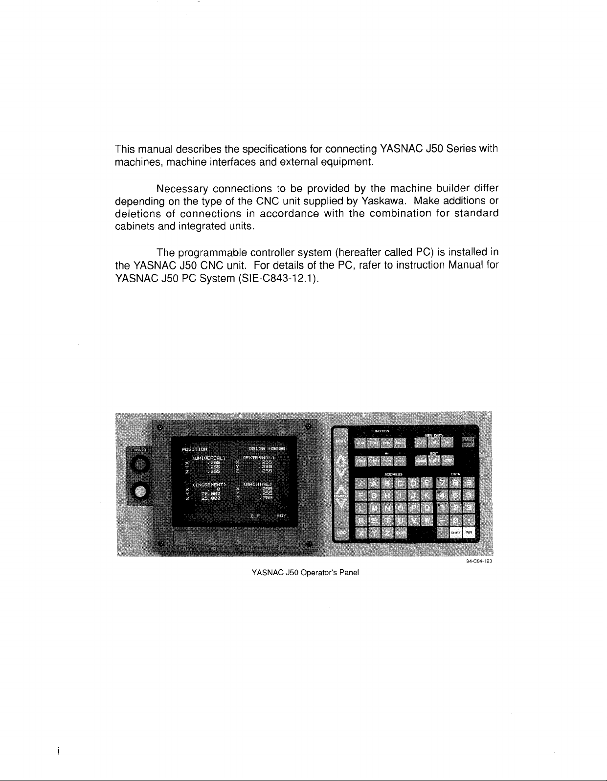
YASNAC J50 Operator’s Panel
94C84123
Page 3

CONTENTS
Page
l. CONFIGURATION. O. . . ..O . . . . . . . . . . . . . . . . . . . . . . . . . . . . . . . . . . . . . . . . . . . . . . . . . . . . . . . . . . ...1
1.1 SYSTEM CONFIGURATION . . . . . . . . . . . . . . . . . . . . . . . . . . . . . . . . . . . . . . . . . . . . . . . . . . . . . . . . . . . 1
I.2STANDARD CABINETS AND INTEGRATED UNITS .. O. . . . . . . . . . . . . . . . . . . . . . . . . . . . . . . . . . . 1
2. ENVIRONMENTAL CONDITIONS. . . . . . . . . . . . . . . . . . . . . . . . . . . . . . . . . . . . . . . . . . . . . . . . . . . . . ...1
3.cABlNET construction DEslGN . . . . . . . . . . . . . . . . . . . . . . . . . . . . . . . . . . . . . . . . . . . . . . . . . . . ..l
4. CABINET DESIGN FORHEAT FACTORS . . . . . . . . . . .. O.O..O... . . . . . . . . . . . .. - . . . . . . . . . ...3
4.1 SELECTION OF HEAT EXCHANGER . . . . . . . . . .. s. . . . . . . . . . . . . . . . . . . . . . . . . . . . . . . . . . . . . . . 3
4.2 HEAT VALUES OF UNITS.. . . . . . . . . . . . . . . . . . . . . . . . . . . . . . . . . . . . . . . . . . . . . . . . . . . . . . . . . ...3
4.3 DUST-PROOF CONSTRUCTION . . . . . . . . . . . . . . . .. $. . . . . . . . . . . . . . . . . . . . . . . . . . . . . . . . . ...4
4.4 PROTECTION FROM MAGNETIC INFLUENCES
5. PRECAUTIONS FOR INSTALLING SERVO UNIT . . . . . . . . . . . . . . . . . . . . . . . . . . . . . . . . . . . . . . ...6
6. CABLE ENTRANCE . . . . . . . . . . . . . . . . . . . . . . . . . . . . . . . . . . . . . . . . . . . . . . . . . . . . . . . . . . . . . . . . ...7
6.1 LAYOUT OF CABLE CONNECTORS . . . . . . . . . . . . . . . . . . . . . . . . . . . . . . . . . . . . . . . . . . . . . . . . . . . 7
6.2 Clamping CABLES AND SHIELDING CABLES• O.OO.O.O... O.. O....• .. O.. O.O.. O.. O.O.O..8
6.3 CONNECTING DIAGRAMS . . . . . . . . . . . . . . . . . . . . . . . . . . . . . . . . . . . . . . . . . . . . . . . . . . . . . . . . . ...9
7. POWER SUPPLY CONNECTION . . . . . . . . . . . . . . . . . . . . . . . . . . . . . . . . . . . . . . . . . . . . . . . . . . . ...12
7.1 POWER SUPPLY CONNECTIONTO EACH UNITO . . . . . . . . . . . . . . . . . . . . . . . . . . . . . . . . . . . . . . 12
7.2 DETAILS OF CONNECTION.. . . . . . . . . . . . . . . . . . . . . . . . . . . . . . . . . . . . . . . . . . . . . . . . . . . . . . . . . 12
8. CONNECTIONTOOPERATOR’S PANEL .o . . . . . . . .. o.c. ..o. .o..o. . . . . . . . . . . . . . . . . . . ...13
8.1 CONNECTION TO EACH UNIT.... . . . . . . . . . . . . . . . . . . . . . . . . . . . . . . . . . . . . . . . . . . . . . . . . . . . 13
8.2 DETAILS OF CONNECTION. O.. . . . . . . . . . . . . . . . . . . . . . . . . . . . . . . . . . . . . . . . . . . . . . . . . . . . ...14
. . . . . . . . . . . . . . . . . . . . . . . . . . . . . . . . . . . . . . . .
5
9.coNNEcTloN oFMANuAL PuLsEGENERAToR . . . . . . . . . . . . . . . . . . . . . . . . . . . . . . . . . . . . ..l5
9.1 CONNECTION TO EACH UNIT.... . . . . . . . . . . . . . . . . . . . . . . . . . . . . . . . . . . . . . . . . . . . . . . . . . . . 15
9.2 DETAILS OF CONNECTION. . . . . . . . . . . . . . . . . . . . . . . . . . . . . . . . . . . . . . . . . . . . . . . . . . . . . . . . . . 16
10. CONNECTION OF INPUT SEQUENCE . . . . . . . . . . . . . . . . . . . . . . . . . . . . . . . . . . . . . . . . . . . . . ...16
10.1 CONNECTION TO EACH UNIT.. . . . . . . . . . . . . . . . . . . . . . . . . . . . . . . . . . . . . . . . . . . . . . . . . . . . . 16
10.2DETAILS OF CONNECTION . . . . . . . . . . . . . . . . . . . . . . . . . . . . . . . . . . . . . . . . . . . . . . . . . . . . . . . . 17
10.3 DETAILS OF SIGNALS..”.. .. ”. .o. .o . . . . . . . . . ..o. o-. o..o..o . . . . . . . . . . . . . . . . . . . . . ...19
ll. CONNECTION TO FEED SERVO UNITS . . . . . . . . .. O. . . . . . . . ..O . . . . . . . . . . . . . . . . . . . . . ...20
ll.ICONNECTION TO EACH UNIT . . . . . . . . . . . . . . . . . . . . . . . . . . . . . . . . . . . . . . . . . . . . . . . . . . . ...20
11.2 DETAILS OFCONNECTION
12. CONNECTION TO SPINDLE DRIVE UNiT . . . . .. O..O. C..O. . . .. O..... . . . . . . . . . . . . . . . . ..”29
12.1 CONNECTION TO EACH UNIT... . . . . . . . . . . . . . . . . . . . . . . . . . . . . . . . . . . . . . . . . . . . . . . . . ...29
12.2 DETAILS OF CONNECTION. ‘ . . . . . . . . . . . . . . . . . . . . . . . . . . . . . . . . . . .. ’ . . . . . . . . . . . . . . ...34
12.3 CABLE SPECIFICATIONS. O. . . . . . . . . . . . . . . . . . . . . . . . . . . . . . . . . . . . . . . . . . . . . . . . . . . . . ...40
13. CONNECTION TO TAPE READER . . .. O. . . . . . . . . . . . . . . . . . . . . . . . . . . . . . . . . . . . . . . . . . . . ...41
13.1 CONNECTION TO EACH UNIT ““. .. ”. .o. .OOOo. . . .. OOO..o. o.oo. . . . . . . . . . . . . . . . . . . . ...41
13.2 DETAILS OFCONNECTION
14. CONNECTION TO RS-232C INTERFACE . . . . . . . . . . . . . . . . . . . . . . . . . . . . . . . . . . . . . . . . ..”- ..42
14.1 CONNECTION TO EACH UNIT . . . . . . . . . . . . . . . . . . . . . . . . . . . . . . . . . . . . . . . . . . . . . . . . . . . . . . 42
DETAILS OFCONNECTION
14.2
14.3 RS-232C INTERFACE .O..O. . . . . . . . . . . . . . . . . . . . . . . . . . . . . . . . . . . . . . . . . . . . . . . . . . . . . . ...43
. . . . . . . . . . . . . . . . . . . . . . . . . . . . . . . . . . . . . . . . . . . . . . . . . . . . . . . .
. . . . . . . . . . . . . . . . . . . . . . . . . . . . . . . . . . . . . . . . . . . . . . . . . . . . . . . .
. . . . . . . . . . . . . . . . . . . . . . . . . . . . . . . . . . . . . . . . . . . . . . . . . . . . . ...42
22
41
ii
Page 4

15. DIRECT-IN SIGNAL CONNECTION
"""" """"""""""""""""'""""""""""""""""""".".""""""" 45
15.1 CONNECTION TO EACH UNIT . . . . . . . . . . . . . . . . . . . . . . . . . . . . . . . . . . . .. - . . . . . . . . . . . . . ...45
15.2 DETAILS OFCONNECTION
. . . . . . . . . . . . . . . . . . . . . . . . . . . . . . . . . . . . . . . . . . . . . . . . . . . . . . . .
15.3 DETAILS OF SIGNALS . . . . . . . . . . . . . . . . . . . . . . . . . . . . . . . . . . . . . . . . . . . . . . . . . . . . . . . . . . ...46
Page
45
16. CONNECTION TOGENERAL-PURPOSE l/OSIGNALS
.. ””””.”.....”””””””.....””””””” 47
16.1 CONNECTION TO EACH UNIT .O. . . . . . . . . . . .. OF. . . . . . . . . . . . . . . . . . . . . . . . . . . . . . . . . . ...47
16.2 DETAILS OF CONNECTION . . . . . . . . . . . . . . . . . . . . . . . . . . . . . . . . . . . . . . . . . . . . . . . . . . . . . ...47
16.3 CONNECTIONTOADDITIONALGENERAL-PURPOSE l/OSIGNALS..O . . . . . . . . . . . . . . . . . 48
16.4 DETAILS OFCONNECTION
. . . . . . . . . . . . . . . . . . . . . . . . . . . . . . . . . . . . . . . . . . . . . . . . . . . . . . . .
48
17. CONNECTION TO GENERAL-PURPOSE 1/0 . . . . . . . . . . . . . . . . . . . . . . . . . . . . .“” . . ..”” ”””””50
17.1 CONNECTION TO EACH UNIT... . . . . . . . . . . . . . . . . . . . . . . . . . . . . . . . . . . . . . . . . . . . . . . . . ...50
17.2 DETAILS OF CONNECTION. . . . . . . . . . . . . . . . . . . . . . . . . . . . . . . . . . . . . . . . . . . . . . . . . . . . . ...51
17.3 EXPLANATION OF GENERAL-PURPOSE l/OSIGNALSO . . . . . . . . . . . . . . . . . . . .“”””. .”””. ”85
18. CABLES
. . . . . . . . . . . . . . . . . . . . . . . . . . . . . . . . . . . . . . . . . . . . . . . . . . . . . . . . . . . . . . . . . . . . . . . . . .
89
18.1 LIST OF CABLES . . . . .. O.. O..... . . . . . . . . . . . . . . . . . . . . . . . . . . . . . . . . . . . . . . . . . . . . . . . . ...89
18.2 SPECIFICATIONS OFCABLE . . . . . . . . . . . . . . . . . . . . . . . . . . . . . . . . . . . . . . . . . . . . . . . . . . . . ...91
18.3 LIST OF CONNECTORS . . . . . . . . . . . . . . . . . . . . . . . . . . . . . . . . . . . . . . . . . . . . . . . . . . . . . . . . . ...93
18.4 SHORTING PIN SETUPS.. . . . . . . . . . . . . . . . . . . . . . . . . . . . . . . . . . . . . . . . . . . . . . . . . . . . . . . ...98
19. J50LSTANDARD VOSIGNALS ‘“ ”” .” .o. .o. ” . . .. o. .o . . . ..o . . ..o . . . . . . . . . . . . . ..”” ”....99
19.1 LISTOFNCSTANDARDl/OSIGNALS . . . . . . . . . . . . . . . . . . . . . . . . . . . . . . . . . . . . . . . . . . . . ...99
19.2 DETAILS OF SIGNALS . . . . . . . . . . . . . . . . . . . . . . . . . . . . . . . . . . . . . . . ...”.”.........””””.” 105
20. J50MSTANDARD VOSIGNALS
. . . . . . . . . . . . . . . . . . . . . . . . . . . . . . . . . . . . . . . . . . . . . . . . . . . .
130
20.1 LISTOFNCSTANDARDl/OSIGNALS . . . . . . . . . . . . . . . . . . . . . . . . . . ...”<. . . . . . ...””””.” 130
20.2 DETAILS OF SIGNALS ”OO””” . .. ”” oo”o”. .. ”” ”O””” . . . ..””. ”o””. ...”.”””””.””.”.””””” 138
APPENDIX ADIMENSIONSinmm . . . . . . . . . . . . . . . . . . . . . . . . . . . . . . . . . . ...””..........””””.. 163
APPENDIX Bl/OPORT ADDRESS SETTING "O. "" O""""""• "".. O""""."".""..• ""O."""""."""" 171
APPENDIX CSTANDARD WIRINGCOLORS OF YASNAC" "O. ".. O"O.O"O"CO.O.".""• "" O.O"O. 174
...
Ill
Page 5
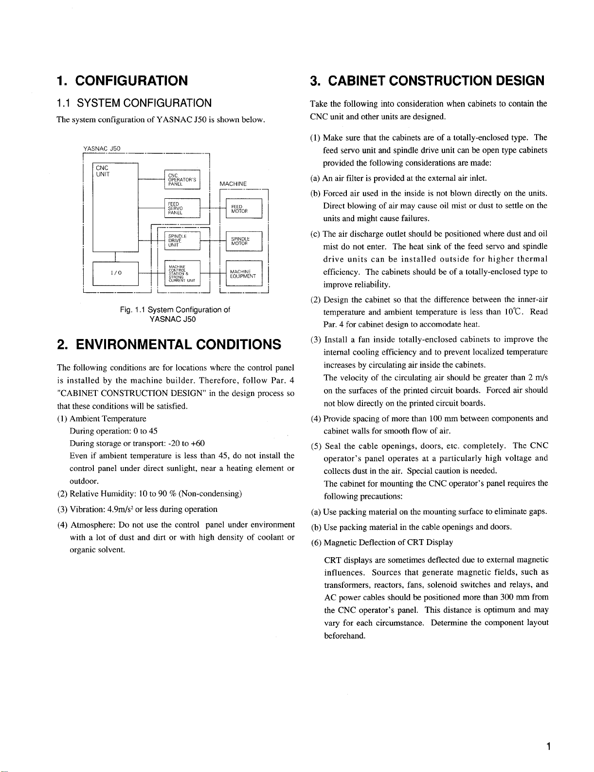
1. CONFIGURATION
3. CABINET CONSTRUCTION DESIGN
1.1 SYSTEM CONFIGURATION
The system configuration of YASNAC J50 is shown below.
ASNAC J50
CNC
UNIT
I I ~
1/0
1
L_._..Jlll!!E!&-
—.— .
L---u w;%’.
Fig. 1.1 System Configuration of
CNC
$IjIP~fTOR S
FEED
Wi:p
~ .-. —._
—.— .—
;WJ;LE
UNIT
i
L._. —._
YASNAC J50
MACHINE
➤✎✿✎✎✍
+=
)
+-El
i-.-.-.–
FEED
MOTOR
MACHINE
EQUIPMENT
2. ENVIRONMENTAL CONDITIONS
The following conditions are for locations where the control panel
is installed by the machine builder. Therefore, follow Par. 4
“CABINET CONSTRUCTION DESIGN” in the design process so
that these conditions will be satisfied.
(1) Ambient Temperature
During operation: Oto 45
During storage or transport: -20 to +60
Even if ambient temperature is less than 45, do not install the
control panel under direct sunlight, near a heating element or
outdoor.
(2) Relative Humidity: 10 to 90 % (Non-condensing)
(3) Vibration: 4.9m/s2 or less during operation
(4) Atmosphere: Do not use the control panel under environment
with a lot of dust and dirt or with high density of coolant or
organic solvent.
Take the following into consideration when cabinets to contain the
CNC unit and other units are designed.
(1) Make sure that the cabinets are of a totally-enclosed type. The
feed servo unit and spindle drive unit can be open type cabinets
provided the following considerations are made:
(a) An air filter is provided at the external air inlet.
(b) Forced air used in the inside is not blown directly on the units.
Direct blowing of air may cause oil mist or dust to settle on the
units and might cause failures.
(c) The air discharge outlet should be positioned where dust and oil
mist do not enter. The heat sink of the feed servo and spindle
drive units can be installed outside for higher thermal
efficiency. The cabinets should be of a totally-enclosed type to
improve reliability.
(2) Design the cabinet so that the difference between the inner-air
temperature and ambient temperature is less than 10°C. Read
Par. 4 for cabinet design to accommodateheat.
(3) Install a fan inside totally-enclosed cabinets to improve the
internal cooling efficiency and to prevent localized temperature
increases by circulating air inside the cabinets.
The velocity of the circulating air should be greater than 2 m/s
on the surfaces of the printed circuit boards. Forced air should
not blow directly on the printed circuit boards.
(4) Provide spacing of more than 100 mm between components and
cabinet walls for smooth flow of air.
(5) Seal the cable openings, doors, etc. completely. The CNC
operator’s panel operates at a particular y high voltage and
collects dust in the air. Special caution is needed.
The cabinet for mounting the CNC opemtor’s panel requires the
following precautions:
(a) Use packing material on the mounting surface to eliminate gaps.
(b) Use packing material in the cable openings and doors.
(6) Magnetic Deflection of CRT Display
CRT displays are sometimes deflected due to external magnetic
influences. Sources that generate magnetic fields, such as
transformers, reactors, fans, solenoid switches and relays, and
AC power cables should be positioned more than 300 mm from
the CNC operator’s panel. This distance is optimum and may
vary for each circumstance. Determine the component layout
beforehand.
1
Page 6
3.
CABINET CONSTRUCTION DESIGN
(Cent’d)
(7)
To prevent malfunction due to noise, mount the units more
than 100 mm from cables feeding 90 VDC or greater, AC
power lines, and other components. The following
precautions should be complied with during wiring:
(a)
Separate AC and DC cables.
(b)
Separate the primary and secondary sides of transformers, line
filters, etc.
(8)
The front panels of the units that are exposed to the cabinet
surfaces, such as the CNC operator’s panel, tape reader, and
PO unit should be of a dustproof type. However, do not install
them in locations where cutting fluid may directly splash on
them. Be sure to seal completely around the mounting
sections.
(9)
Mount the units so as to allow easy checking, removal and
reinstalling during maintenance work.
(10) Read the instruction manuals of the feed servo and spindle drive
units when mounting them. Heat sink should be installed outside
the cabinet to reduce internal thermal losses. This increases the
possibilities for a change from an open type to a totally-enclosed
type and reduces the capacity of the heat exchanger.
(b) Provide spacing of more than 50 mm in the upper section and
100 mm in the lower section of the unit for better ventilation
and easier maintenance.
(c) For ventilation or maintenance, provide spacing more than 50
mm from the upper side and more than 100 mm from the lower
side of the CNC unit.
● Example
RADIATOR
FIN
AIR
4
FEED SERVO AND
3-
* \
J-
-+ PINDLE DRIVE UNITS
(11) Precautions for Mounting CNC Unit
Observe the following points particularly during mounting of
the CNC Unit:
(a) Mount the unit in the direction shown in Fig. 3.1.
(UP)
n
(DOWN)
Fig. 3.1 Mounting of CNC Units
n
2
Page 7

4.
CABINET DESIGN FOR HEAT
FACTORS
4.2 HEAT VALUES OF UNITS
4.2.1
NC UNIT
4.1
SELECTION OF HEAT EXCHANGER
The
cabinets to contain the CNC unit and other units should beef a
totally -enclosed type. The inner-air temperature differential inside
the cabinets should be less than 10”C. Heat exchangers may be
needed inside the cabinets depending on the heat generated by the
installed electric equipment. Determine the heat exchanger
capacity as follows :
AT: Air temperature rise inside cabinet (“C)
Pv : Total heat generated by electric equipment (W)
k : Cabinet heat transmission [W/(m2 . ‘C)]
Calculate based on 6W/(m’ ‘C) if a circulating fan is
installed.
A : Effective radiation area of cabinet (m’)
qh : Heat exchange ratio of necessary heat exchanger.
1. Calculate the total heat value Pv of the electric equipment.
Pv=Z (Heat value of each unit)
2. Calculate the effective heat radiation area A.
x {W (width) x H (height) }+ 2 {W (width)
A=2
x D (depth)] + 2 {D (depth) x H (height))
The surfaces that are not exposed to external air are ineffective
areas.
L
A
A
~ : INEFFECTIVE AREAS
Note : If 50 mm or less from the floor,
bottom areasare ineffective.
Table 4.1 Heat Values of NC Unit
Unit I Heat Value (W)
103
17
25
5
4.2.2
CNC Unit*
CNC Operator’s Panel
I
I
Tape Reader
1/0 Module
Heat value of CNC unit changes by adding the option.
*
I
SERVO UNIT
Table 4.2 Heat Value of Servo Unit
Type
Unit
SGDB-
05AD
lOAD
15AD
20AD
30AD
44AD
60AD
75AD
1AAD
Notes :
1.The servo unit uses two shafts, and its load factor should be 70 to 80%.
2. The internal heat value is the heat value remaining inside if the heat fin
is installed outside.
3. Heat value created by regenerative resistance will differ depending on
the frequency of rapid feed starts and stops.
4. Regenerative circuits are incorporated in the unit types SGDB-05 to
1A and are mounted externally for the types SGDB-60 to 1A as
options.
5. Capacity of regenerative circuit is calculated by 200% of allowable
dissipation.
Total Heat
Value (W)
50
70
I
90 45
I
130
180
I
210 105
I
370 135
480 240
600 300
Internal Heat
Value (W)
I
I
25
35
65
90
Regenerative
Resistance (W)
28
28
I
28
28
28
I
28
3. Calculate the allowable heat value Pv’ that ensures the
temperature increase within cabinet (AT) to be less than 10°C.
Pv’=k. A. AT (W)
Llo”c
L-
6W (mz. “C)
4. A heat exchanger is not needed if total heat value Pv S allowable
heat value Pv’.
5. A heat exchanger has to be installed with the following heat
exchange ratio (heat exchanger capacity) qh if total heat value
Pv > allowable heat value Pv’.
(pv-pv’)/ AT (W/”C)
qh=
Llo”c
3
Page 8

4.3 DUST-PROOF CONSTRUCTION
Particles floating in the air (dust, cuttings, oil mist, etc.) may cause
malfunction of the CNC unit and the inner parts of theotherboads
(particularly CRT) to be mounted inside the cabinets the machine
manufacturers design and build. The construction of the cabinets,
therefore, should be such that it does not allow dust, etc. to enter
inside.
(1) The cabinets should be of totally-enclosed construction.
(2) Sealthe cable openings withpacking. (See Fig.4.1.)
(3) The door and the back cover should be securely sealed with
packing. (See Fig.4. 2.)
(4) Special caution is required for the CNC operator’s panel as it
operates at high voltage and collects dust in the air. The
following points should be observed with regard to the pendant
box used to install the CNC unit.
(a) Seal the cable openings,
eliminate gap.
(b) Packing is attached on the surface where the CNC operator’s
panel istobe mounted. Usethependant boxas it is.
(5) Seal all gaps.
(6) Oil mist easily settles on the ceiling and enters the cabinets
through screw holes. Special precaution, therefore, should be
made using oil-proof packing, etc.
dooi.” back cover, etc. with packing to
Page 9

(Reference) Neoprene sponge rubber (belongs
tochloromene rubber) isrecommended for the
ial.
METAL FITTINGS
PACKINGS
f
PENDANT BOX
Fig.4.l Cable Entrance
Fig. 4.2 Door Packing
PLATE
~NC OPERATOR’S PANE1
Fig. 4.3 CNC Operation’s Panel
4.4 PROTECTION FROM MAGNETIC INFLUENCES
The CRT display may be deflected due to external magnetic
influences. Sources that generate magnetic fields (such as
transformers, reactors, fans, electromagnetic switches, solenoid
relays, AC power cables) should be kept about 300 mm away
from the CRT display.
This distance of 300 mm is a rule of thumb and the optimal
distance may differ for each setting. Therefore, full precaution
should be given to location of the above components that generate
magnetic fields and determine the final layout after checking the
condition of the CRT display.
5
Page 10
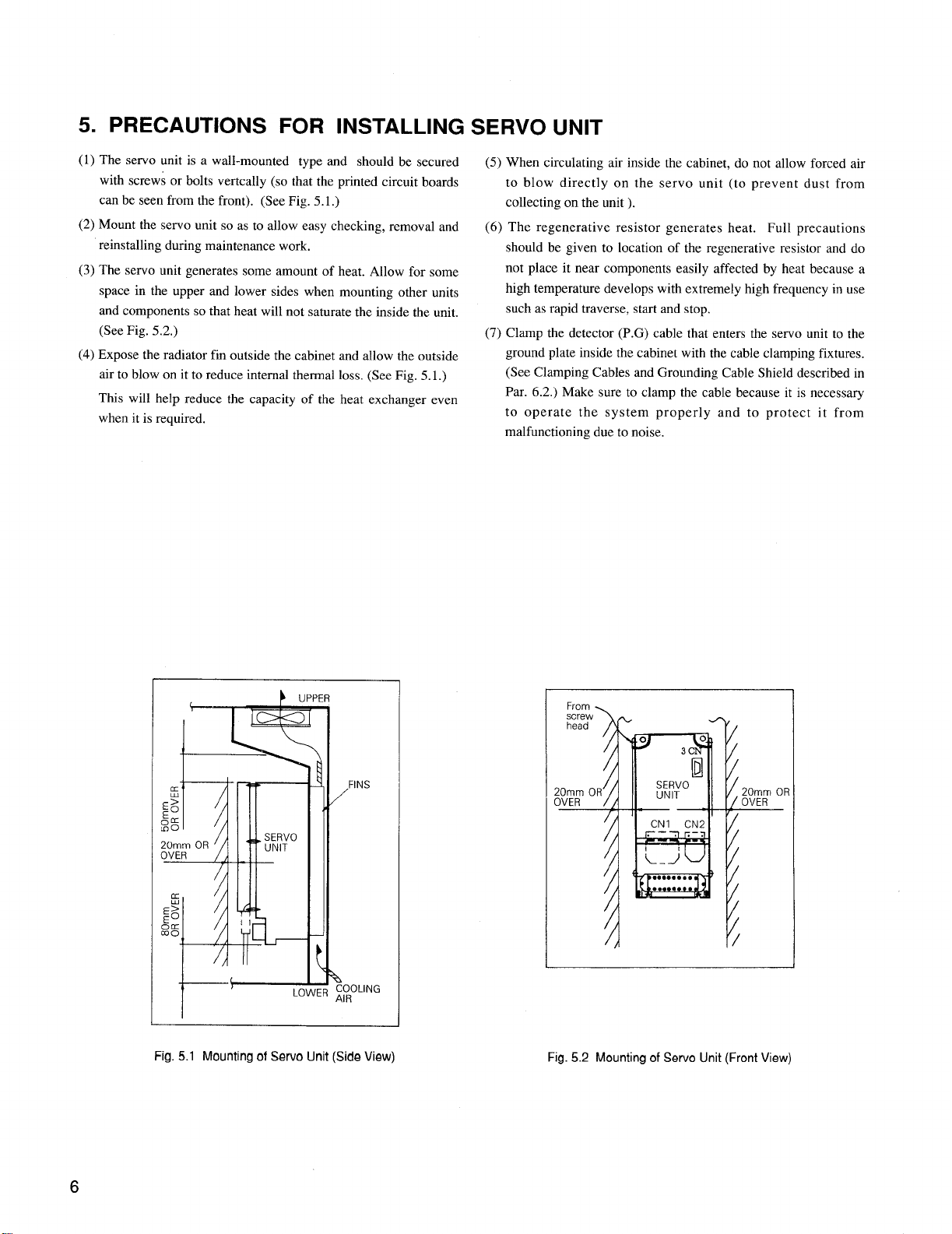
5. PRECAUTIONS FOR INSTALLING SERVO UNIT
(1) The servo unit is a wall-mounted type and should be secured
with screws or bolts vertcally (so that the printed circuit boards
can be seen from the front). (See Fig. 5.1.)
(2) Mount the servo unit so as to allow easy checking, removal and
reinstalling during maintenance work.
(3) The servo unit generates some amount of heat. A11owfor some
space in the upper and lower sides when mounting other units
and components so that heat will not saturate the inside the unit.
(See Fig. 5.2.)
(4) Expose the radiator fin outside the cabinet and allow the outside
air to blow on it to reduce internal thermal loss. (See Fig. 5.1.)
This will help reduce the capacity of the heat exchanger even
when it is required.
(5) When circulating air inside the cabinet, do not allow forced air
to blow directly on the servo unit (to prevent dust from
collecting on the unit ).
(6) The regenerative resistor generates heat. Full precautions
should be given to location of the regenerative resistor and do
not place it near components easily affected by heat because a
high temperature develops with extremely high frequency in use
such as rapid traverse, start and stop.
(7) Clamp the detector (P.G) cable that enters the servo unit to the
ground plate inside the cabinet with the cable clamping fixtures.
(See Clamping Cables and Grounding Cable Shield described in
Par. 6.2.) Make sure to clamp the cable because it is necessary
to operate the system properly and to protect it from
malfunctioning due to noise.
s
ING
Fig. 5.1 Mounting of Servo Unit (Side View)
From .
R
Fig. 5.2 Mounting of Servo Unit (Front View)
Page 11

6. CABLE ENTRANCE
6.1 LAYOUT OF CABLE CONNECTORS
CNC UNIT TYPE JZNC-JRKOO
n
P%l CP50
BA
TTERY
#
m
SR50
‘R50
1
o
D
!
o
D
&
]
D
u
YASNAC
Lc
m
z
v
e
m
z
o
SUORCE ~
POWER ON O
m
m
z
o
F
AiM
N
m
z
v
z
z
o
CN03
01
N
+5V0
+24V O
OHT O
CN02
01
M
CNO1
=3==
—
4
Fig.6.l Layout of CNC Unit Connectors
m
z
v
r
J
1
01
M
7
Page 12

6.2 CLAMPING CABLES AND SHIELDING CABLES
Of the cables connected to the YASNAC, clamp those that need
shielding to the ground plate securely with the cable clamping
fixtures as shown in the figure below. This clamping serves not
only as cable support but also as cable shielding. In ensuring safe
operation of the system, it is extremely important that you clamp
the necessary cables without fail.
CABLE
SHIELD
ENCLOSURE
ABLE CLAMP
(a) Strip part of the cable shield as shown in the figure below to
expose the shield enclosure.
Press the exposed part onto the ground plate using the cable
clamp.
(b) Mount the ground plate near the cable opening.
(c) Stripping cable enclosure is not required for non-shielded cables
for clamping.
TYPE 1
DF8401485
19.5
TYPE 2
DF8404817
-=3252s2--
‘CABLE
Fig. 6.2 Shielding Cables
Page 13

6.3 CONNECTING DIAGRAMS
(1) YASNAC J50L (For Lathe)
~NAc-J50L
— -— -—
ACK B
J
—
JANC
CNAI
CNF
ZNA2
:ND1
CNE
c
BE
cl
IE1----i
IC---i
POWER SUPPLY
MOOULE
CPS.18FB
a
PC BOARD
JANCD PC50
CNA
~Aif$D
10~lON)
D
n
CNF
D
CPU BOARD
JANCD CP50
CNA
o
CNO
r
,Xls 80AR0
ANCD.SR50. 1
7
JANCD BB51
BATTERY
CNM
FAN
CNO1 ~
CN02 D
CN03 r+
CN12 ~
CN13 ~
CN1l }
CN1O ~
CN2(
CN30 ~
CN31
I
200VAC
I
1
-a--l-J
J p~=’mr-
ENET @
u @l,owER,NpuT,EouENcE,
@
@ p~R TYPE ,APE
S 232C
cl-
E
= (OPTION)
READER
OPERATORS PANEL
OPERATION PANEL
FOR MACHINES
pp & -~ ~-
[/0 MODULE
CN 1
,N2 ‘iii
CN3 @‘
CN4 ‘m ,N40M,NT,
@, q CN’3 :;; ,@
‘ +&f
CN14
—.—. —
CONTROL CABINET
@
L. —-—
II
1/0 MODULE
JANCD. EC860
CN1l
CN12
?
L.—
1/0 MODULE
+
r
/+
CN13
CN14
JANCD ?C861
CN1l
CN12
CN13
[- ]h
Kfl
a
::; ‘@‘ ;:I;::UT8WINTS
CN3 @
U
,N4 ‘e ,NWPO,NTS
CN5 B
Zt
CN6 ‘*‘ :;:::Ts
d-t
.—. J L.
CN1 a
F
,N2 @~
CONTROL CAB! NET
C61
CONTROL CABINET
— .—
OUT40 PUNTS
IN 8 FOINTS,OUT 8 FONTS
IN24 POINTS,OUT 16POINTS
IN 40 POINTS
OUT32 FONTS
IN
DIRECT
IN 24 FtlNTS, OUT 16 POINTS
.— .—
IN 24 POINTS,OUT 16POINTS
IN 24 POINTS,OUT16POINTS
;ND2
:.:.*:Y:Y
ill
ND
[
Fig. 6.3
9
Page 14
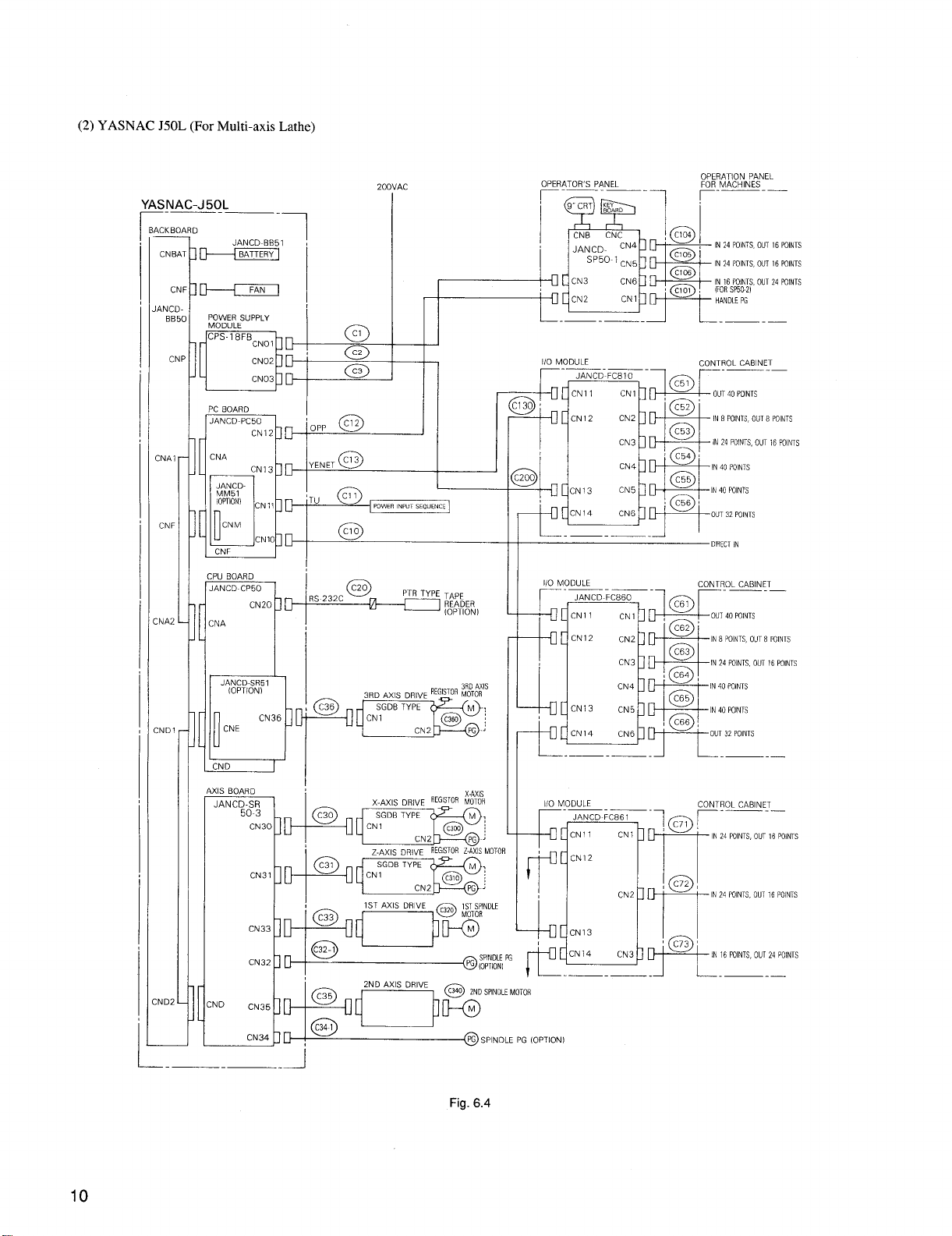
(2) YASNAC J50L (For Multi-axis Lathe)
YASNAC-J50L
--— ___
I
\CKBOARD
CN
ICt---l
IH
AN(
B
(
Imd=+#
1
PC BOARD
,mQ lop’ @
ZNA
CN
:NA
:ND
CNA
JANCDMM51
(OWION)
CNM
!
~j
CNF
?20-$:~~
JANCD-SR51
F
OCNE c“” P=
JANCD !3B51
BATTERY
FAN
CN13
CN1l
CN1O
(OPTION)
@
C62
OPERATION PANEL
FOR MACHINES
~.—.—
CONTROL CABINET
CONTROL CABINET
IN 24 POINTS,OUT 16POINTS
OUT 32 POINTS
DIRECT1“
N 8 POINTS,OUT8 POINTS
IN 24 POINTS,OUT 16POINTS
200VAC
I
I
I
I II
& YENET c“
~ ‘T. @ ,POwERINPuTs,OUEN~ ‘ ‘+ CN’3 :; ~% ‘N40m’NTs
c)
2 --.H
n
@
OPERATOR’S PANEL
~.p.—.
I e- I
1/0 MOOULE
~-7d_
4-
@’ ;
CN1l
CN12
l----v
@
CN14
1/0 MOOULE
r
CN1l
“c~*:4=--
CN12
If~
CN13
-% CN14 ‘B’
7
::: W::I:::UT8POINT$
CN3 @
ti
CN4 ‘@’ ,N40POINT,
n
-w
CN3 @
ti
CN4 ‘@‘ ,N40,01NTS
CN5 @ ,N40POINT,
a
CN6 n~ow 32 POINTS
L--
1/0 MODULE
JANCD-~C8~:1 ‘lo r-—-–
CN1l
4-
CN12
~~–-~
1ST AXIS ORIVE @ /jlX~NOLE
CN33
CN32
:ND
—
4$=--RPINDLEP:(:---”” ‘----
‘: n~ +jcN’ ,N3~Dl@~
1P
‘No‘x’s‘“v’ @
SPINDLEPG
pG (OPTION)
2NDSPINDLEMOTOR
Fig. 6.4
CN14
P
,N, @
CONTROL CABINET
IN 24 POINTS,OUT16POINTS
IN 24 PilNTS, OUT 16 POINTS
IN 16 POINTS,OUT24 POINTS
Page 15
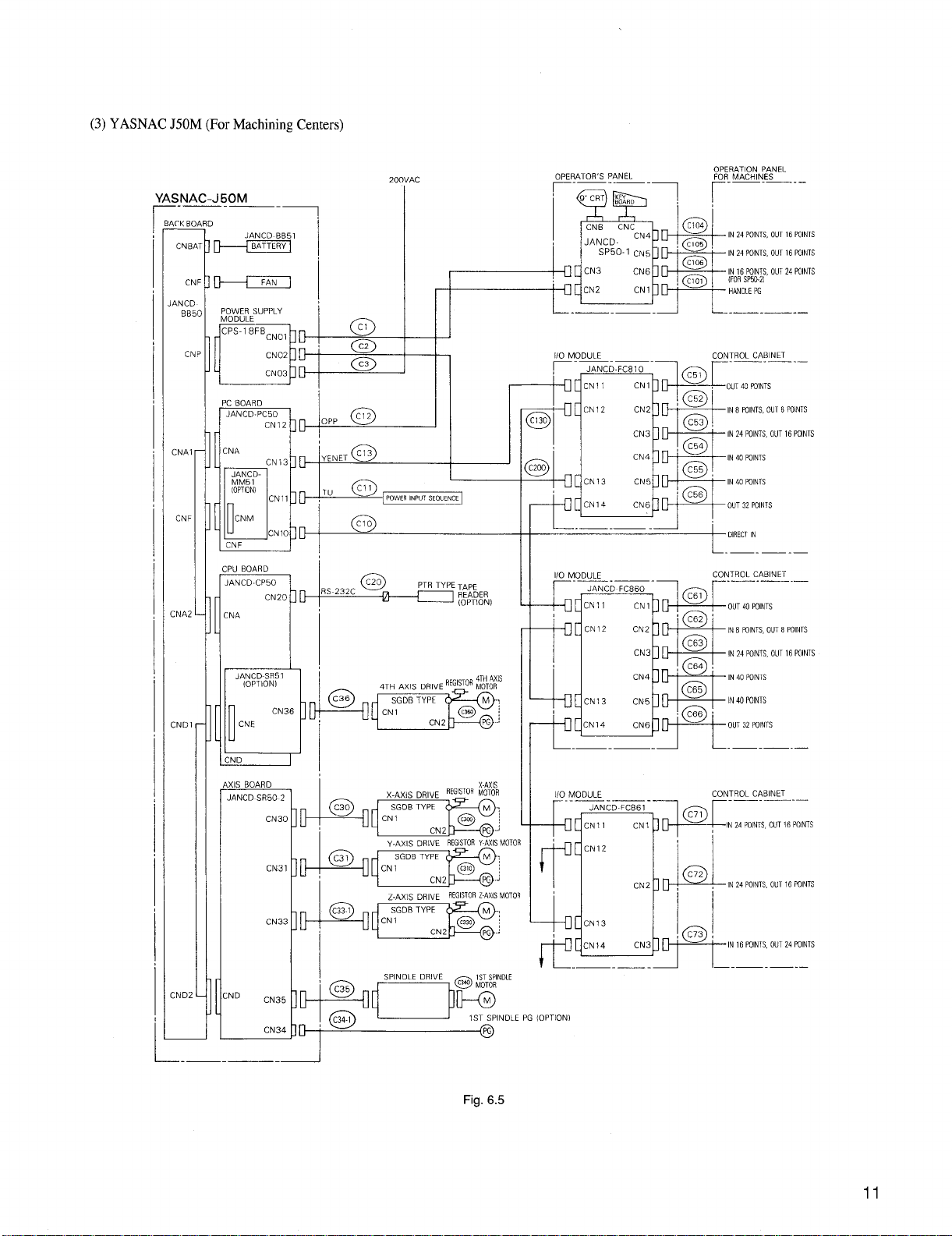
(3) YASNAC J50M (For Machining Centers)
ASNAC-J50M
—-
—. —-—
V-K E
Ctil
c
ANC
BE
c
CNA
i b“
CNI
CNA
CND
n ,-.,, ”
~l~~fl~cNIOp”~ @$ ‘ f-w”
CPU BOARD
JANCDCP50
CNA
n
CND
L
JANCD BB51
BATTERY \
...
MM51
IOPTIONI
JAN CD-3R51
(OPTION)
CNE
o
X15 BOARD
~
200VAC
OPERATOR’S PANEL
—- —-— -=
I
CNC
CNB
FAN
J
l_._~.J
1/0 MOOULE
JANC6.FC81O
,r -
CN1l
@l CN’2 ::: @ :::’’,0:::’,,
@
,ml,u- 0 ...... .. .... .. CN’3 :: ,:’’”40’0’”’s
CN1l
..””,” ,.!’., >,..,,,.,
i —’ II
CN20
CN36
$~~fi
I
L-.—
1“0 MOOULE _
CN1l
“Fc8::-dfy=:”-
CN12
f~~
CN13
CN14
?
L.—- —.2 L. —. —.—..—
100 MOOULE
CN1 @ ;“,40,0,,,,
,N4 ‘@ ,N40POINT;
._.>
CN3 a
~N4 ‘e ,N40POINTS
CN5 e
CN’ *0uT32p0’NTs
OPERATION PANEL
FOR MACHINES
.- —-—
.—
L--------
CONTROL CABINET
v-
xs
CONTROL CABINET
C62 ‘
E
am
CONTROL CABINET
.— .—
OUT 32 FYIINTS
OIRECTIN
1“8 POINTS,OUT8 POINTS
IN 24 POINTS,OUT 16POINTS
IN40P!INTS
CND
LT–
-h=bla==is
z-AXIS DRIVE REGlsToRz-4xls MoTol
CN33b~nm
II
.E PG (OPTION)
Fig. 6.5
11
Page 16

7. POWER SUPPLY CONNECTION
7.1 POWER SUPPLY CONNECTION TO EACH UNIT
CNC UNIT
—-~
—.
CPS-18FB
172039-1
m
3
G
4
CN 03
ld-----
7
w
Fig. 7.1
7.2 DETAILS OF CONNECTION
I
C03
172025-1
POWER
SUPPLY
:Ps
CN3-3-T-G
1
SINGLE-PHASE
200/220/230VAC f 15°A
!i13/IW)H7 +2Hz
580VAC
T
T
NOTE: The power supply is designed to function normally even in the event of l/2-cycle
or shorter momentary power loss or 1-cycle or shorter 50% voltage drop.
Fig. 7.2 Power Supply Connection
12
Page 17

8. CONNECTION TO OPERATOR’S PANEL
8.1 CONNECTION TO EACH UNIT
JANCD-PC50
CNC OPERATOR’S PANEL
JAN CD-SP50
I
10220
172040-1
CPS.18FB
CNIZ
CNO1
1
C12
1012O-3OOOVE
Col
172026-1
+
01’D3000VE
+
-1782W5
1
CN2
10220-6202J L
CN3
1-178315-2
IEB
1 +5V
2 05V
3
4 +24V
5 O,,v
CN3 PIN
POSITION
Ka%zl
Fig. 8.1
Page 18

8.2 DETAILS OF CONNECTION
CNC UNIT CNC OPERATOR’S PANEL (CRT/P)
TYPE JANCD-PC50
-_—-
3
CN 12-4
CN 12-5
~.
-—
‘1
I
I
SIG II
* SIG
! ,
11
/ P,
“ P
TYPE JANCD-SP 50
I
CN2-4
CN2-5
4’-t--=h+
CN 12-13
CN 12-12
CN 12-1 VIDEO
CN 12-2
CN 12-8
i
~___J
TYPE CPS-18F8
r
~: ; ~ 1;
CN 12-9
CN 12-18
CN 12-19
CN 12-16
CN 12-17
CN 12-20
2!E
I I *1 1
-—-
CNOI - 1
5V
+
CNO1- 4
.
CNO1-3
+24V
CNO1-5
,.
3 ‘~
-—-
* vIDEO
* HLGT
: HSYNC CN 2-19
; VSYNC
POFF
PCOM
HLGT
HSYNC
VSYNC
FG
II
II
II
I ~1
II
I pl
II
I pl
II
I pl
(1
CN 2-13
CN 2-12
CN 2-I
CN 2-2
CN2-8
CN2-9
CN2 -18
CN Z-16
CN 2-17
CN 2-20
!/
CN3-1
CN 3-2
CN3-4
CN 3-5
Vertical type CNC contains a power ON/OFF switch.
*
A special external circuit does not have to be provided.
Notes:
1. The shield enclosure does not have to be grounded outside.
2. Power ON/OFF can be selected by the panel power ON/OFF (POF)
and/or remote power ON/OFF (EOF) by a shorting plug.
Setting in Main board
model JANCD-PC50
Sw 2
~o
1
3 + EoF
(INEFFECTIVEIEFFECTIVE
NV3
1 o~ 3 + ~g:FEcTlvE,EFFEcTlvE)
Settings prior to
factory shipment
Fig. 8.2 Connecting Power Unit (Type CPS-18FB) and PC Board (Type JANCD-PC50)
to CNC Operator’s Panel (CRT/P)
14
POWER ON
POWER OFF
PON
POFF
PCOM CNB -20
I
L
SW2, SW3 Setting
Panel/Power RemotePower Paneland Remote
ONIOFF(POF)ONIOFF(EOF) PowerONIOFF
OFFION
‘w’ ‘m’
CNB -18
CNB-19
OFF/ON
‘m’ ‘ma
Sw3 1m]3 lm13 1m3
.—
.
OFFION
Page 19

9. CONNECTION OF MANUAL PULSE GENERATOR
9.1 CONNECTION TO EACH UNIT
CNC OPERATOR’S PANEL
-~
JANCD-SP50
10220-6202JL
—
CN 1
1 OVH 11
2 OVH 12
3 OVH 13
4 +5VH 14
5 +5VH 15
6 +5VH 16 PAH
7 17 *PAH
8 18 PBH
9 19 *PBH
10
El
20 FG
ID
I
I
Fig. 9.1
Clol
10120-3000
V E
15
Page 20

9.2 DETAILS OF CONNECTION
1st Manual Pulse Generator
(1)
10. CONNECTIONOF INPUTSEQUENCE
10.1 CONNECTION TO EACH UNIT
L.-1,
I + L-.—
(OPENCOLLECTORfi
UT]
_.—
CNC OPERATOR’S
PANEL
“pE ‘:fpj ~pfm
CN 1-6 +Wi
r
CN 1-4 +5VH I
CN 1-1 OVH : p: 2
CN 1-16 PBH : : s p~
CN 1-2 OVH 1P,
CN 1-18 PBH : : 4
CN 1-3 OVH
%
[
—.
----
;&:E~PERATOR’S
TYPE JANCD-SP50
—.—-----
.“7 r-—”—”—
CN 1-16 PAH :-,,
r-”
CN 1-17 * PAH
CN 1-18
I
I
I
. PBH
CN 1-19.*PBH
CNI-4,i 6
CN1-),2,3
OVH
CN 1-20 FG !!
—.—
ii
Notes:
1. The HPG power supply is a constant +5V.
2. An open collector (cable length 5 m or less) or differential output (cable
length 5 m or more) can be used for HPG output.
3. Shielded cables are not needed if the cable lengths are less than 1 m.
Twisted-pair cables can be used. Use twisted-pair shielded cables if the
cable lengths are more than 1 m and ground the cable shield enclosure
using a ground plate inside the panel or CN 1-20 pins (FG).
No 1 MANUAL PUI
GENERATOR (1 HP
,..
PI
p,’
‘7
L._._
(OPENCOLLECTOROUTP
No. 1 MANUAL PULSE
GENERATOR II HPG)
(OIFFERENTIAL”OUTPUT”fi1
;E
1)
ITI
1
PE)
CNC UNIT
JANCD-PC59
1OZO-52A2JL
10 20 FG
s
%,,,5,23=-
50/60Hz
—
1 11 +24VT
2 12 TCOM
3
4 14
5 15
6
7 TON 17 SVMX
8 18 NCMX
9
13 ‘OFF
16 *TOLO
19 *TESP
MAIN CIRCUIT
CN1”
s.ivm (~BRAKE UNIT
=TAPEREADER
Fig.
Qwl
D
1012O-3W3VE
FEED SERVO UNIT (MAIN CIRCUIT)
FEED SERVO UNIT (CONTROL CIRCUIT)
10.1
POWER ON
INTERFACE
Page 21
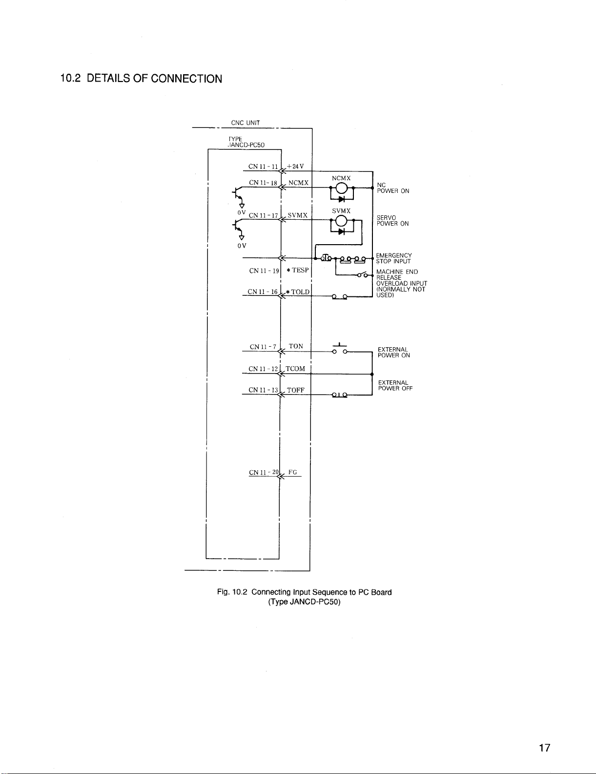
10.2 DETAILS OF CONNECTION
Ft!?!!
—.
CNC UNIT
rYPE
,IANCD-PC50
CN II-I
CN 11-1[
r
0“ CN1l -1’
Ov
CN1l-1
CN 11- 1[
CN1l-7
CN 11-1:
CNII -1:
-~
,+24V
.NCMX
NCMX
NC
POWER ON
=ka
“7
SVMX
J-
SERVO
POWER ON
EMERGENCY
STOP INPUT
MACHINE END
RELEASE
OVERLOAD INPUT
(NORMALLY NOT
USED)
EXTERNAL
POWER ON
SVMX
TESP
*
TOI.D
,*
TON
TCOM
TOFF
CN1l-2
.-—_—
Fig. 10.2 Connecting Input Sequence to PC Board
FG
(Type JANCD-PC50)
Page 22

The connection example of the PC board is shown below.
Rts:FEEDsERvO”N’T
1- ‘“”v’c~
NCMX
SVMX
K
200/220/230VAC, 50/60Hz
RSTE
n NCM
m SVM
NC POWER ON
)
(LJSe Contactor equivalent to Hi. )
SERVO POWER ON
(Use contactor eqwalent to H1. Determine contact
capawy according to the servo unit, etc. )
II
Rs
-u----s
I
NCMX
‘L
svnJlx
.—.
1:5
I i–-—_—
I BRAKE POWER SUPPLY
OPR1O9ATYPE FOR 200/220VAC INPUT
/ [OPR1O9F TYPE FOR IOOVAC INPUT
T
IL
1! ———— ——— ——— .—
k=+
TO FEED SERVO UNIT
Ts
EMERGENCY STOP PB
MOTOR BRAKE 1
‘ :=:] ~NOte’
-i
1
\
I
I
Required only for using
holding brake.
The brake is built m the
motor.
,
I
I
I
—u----> :––– ——=—––”-”
Fig. 10.3
TAPE READER
Page 23

10.3 DETAILS OF SIGNALS
10.3.1 NC POWER ON (NCMX) AND SERVO POWER
(SVMX)
ON
(1) NCMX: This output is turned ON when the logic circuit of the
control is energized.
(2) SVMX: This output is turned ON when the servo unit is
energized. With an external servo unit, turn ON the power
supply when this signal is outputted.
(3) The power supply turning ON sequence is as follows:
(a) Close the power supply main switch for the control.
(b) Either push the POWER ON button on the CNC operator’s
panel, or close the circuit between EON and ECM. Then, the
logic circuit and the servo control circuit are both energized,
and the circuit between NCMX (NC power input and output) is
closed.
With an external servo unit, design the servo control
circuit power input sequence so that the circuit is
energized at the output of NCMX signals.
:
(c) Again make the same power switching (pushing the POWER
ON button or closing the circuit between EON and ECM).
Now, the servo power supply is turned ON, and the circuit
between SVMX (servo power input and output) is closed.
:
10.3.2 EMERGENCY STOP (TESP) INPUT
When the circuit between emergency stop input terminals (TESP) is
open, the control stops totally the servo power supply is turned off,
and the emergency stop output (*ESPS) of general purpose 1/0
module is opened.
10.3.3
EXTERNAL POWER ON-OFF (EON, EOF,
ECM) INPUT
The control can be switched on and off by external input signals, in
the same way as the depressing of the POWER ON/OFF buttons on
the CNC operator’s panel. When the circuit between EON and
ECM is closed, the logic circuit or servo power of the control is
energized. When the circuit between EOF and ECM is opened, the
logic circuit or servo power of the control is deenergized.
=L:-
CONTROL SERVO
POWER SUPPLY
Fig. 10.5 External Power ON-OFF
With an external servo unit, design the servo power
circuit power input sequence so that the circuit is
energized at the output of SVMX signals.
:
(d) When the external circuit is ready after the circuit between
SVMX is closed, and the control becomes ready, close the
MRD (machine ready) input of the 1/0 module. Then, RDY is
displayed on the CRT, and operation becomes possible.
POW;: ON
NCMX
(OUTPUT)
SVMX
(OUTPUT)
MRD
(INPUT)
n
\
+
:~p~:tEEN
ALARM CODE
“31 o“
Fig. 10.4 Time Chart of Power Supply
Turning on Sequence
n
I
, i_
:;;FW:;EEN ;YSCCYREEN
ALARM CODE
“280
‘“ROY” DISPtAY
:
10.3.4 OVERLOAD (*TOLD) INPUT
Short-circuit T24(CN11- 16) if this input is not used. (Normally
this input is not used.)
Page 24

11. CONNECTION TO FEED SERVO UNIT
11.1 CONNECTION TO EACH UNIT
For Lathe
(1)
CNC UNIT
10226 -52A2JL
—
JANCDSR51 1
JAN CD SR502
CN33
—
FEED SERVO UNIT
SGDB TYPE
CN1
1025O-52A2JL 1022O.52A2JL
1 PGOV 11 BAT I
2 PGOV 12 BAT+
3 PGOV 13 BAT–
4 PG5v 14 PC5
5 PG5V
6 PG5V 16 PA5
7 DIR
8 Ps 18 PB5
9 *PS 19 *pB5
10 20 FG
❑
CN2 PIN LAYOUT
(3RD AXIS)
CN2
15 *PC5
17 *PA5
1
1o120-
3000VE
~
FEED MOTOR
C360
PG
a
In
10226 -52A2JL
CN31
CN30
— —
Fig. 11.l Cable Connection between lst Axis and3rd Axis
C31
1
)126-30d0 E
L
II
II
b
iO150-3000VE
J
‘1
FEED SERVO UNIT
SGDB TYPE
1
SGDB TYPE
CN
1 CN2
1025O-52A2JL 10220-52A2J L
1 PGOV
2 PGOV 121BAT+
3 PGOV
4 PG5V 14 Pcl
5 PG5V
,6 PG5V 16 PAI
7 DIR 17 *PA1
8 Ps
9 * Ps
10
CN2 PIN LAYOUT
1
(2ND AXIS)
(1ST AXIS
ll]BATI
13 BAT–
15 * pcl
18 PB1
19 * PB1
20 FG
C31o
1
1o1203000VE
n
C300
1
1o1203000VE
n
FEED MOTOR
PG
d
FEED MOTOR
PG
G
20
Page 25
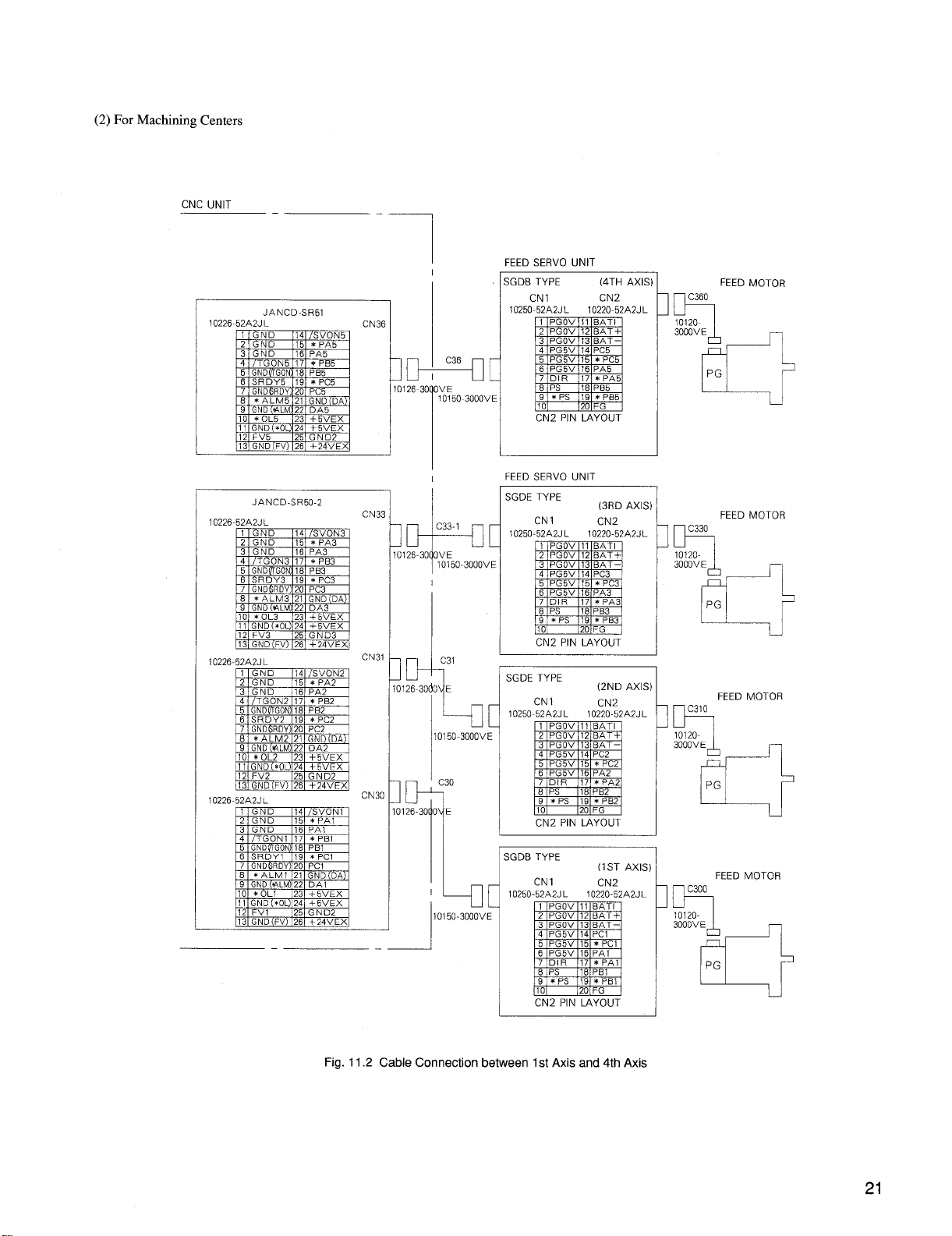
(2) For Machining Centers
CNC UNIT
I ( II
10226-52A2J L
10226
—
JAN CD-SR50-2
—
7
CN3:
1
10126-30 OVE 2 PGOV 12 BAT+
CN31
1~
10126-30d0 E
CN3C
1
10126-300 E
—
I
I
I
I
C33-1
1015O-3OOOVE 3 PGOV 13 BAT–
+
C31
I I -d
w
1015O-3OOOVE
C30
9
II
L
1015O-3OOOVE
FEED SERVO UNIT
SGDB TYPE
CN 1
1025O-52A2JL
10 20 FG
s
CN2 PIN LAYOUT
FEED SERVO UNIT
SGDE TYPE
CNI
1025O-52A2JL 1022O-52A2JL
10 20 FG
!:
1=[
I
CN2 PIN LAYOUT
I
SGDE TYPE
CN1
1025O.52A2JL 1022O-52A2JL
8 PS 18 PB2
10 20 FG
CN2 PIN LAYOUT
I
SGDB TYPE
CNI
10250-52A2J L
2 PGOV 12 BAT+
3 PGOV 13 BAT–
4 PG5V 14PC1
5 PG5V 15 *PC1
6 PG5V 16PA1
7 DIR 17 *PA1
6 PS 16 PB1
9 *PS 19*PB1
s
:N2 PIN2:Y:UT
(4TH AXIS)]
CN2
1 PGOV 11 BAT I
2 PGOV 12 BAT+
3 PGOV 13 BAT–
4 PG5V 14Pc5
5 PG5V 15 *PC5
6 PG5V 16PA5
7 DIR 17 *PA5
8 PS 16 PB5
9 *PS 19*PB5
1 PGOV 11 BAT I
4 PG5V 14 PC3
5 PG5V 15 * PC3
6 PG5V 16 PA3
7 DIR 17 * PA3
8 Ps
9 *
1 PGOV 11 BAT I
2 PGOV 12 BAT+
3 PGOV 13 BAT–
4 PG5V 14PC2
5 PG5V 15 *PC2
6 PG5V 16PA2
7 DIR 17 *PA2
9
1 PGOV 11 BAT I
1022O-52A2JL
18 PB3
Ps 19 * pB3
*PS 19*PB2
1022O-52A
(3RD AXIS)
CN2
(2ND AXIS)
CN2
(1ST AXIS)
CN2
C360
1o120-
3000VE
h
PG
la
IF%
1o1203000VE
A
PG
n
I
L
C31O
b
1o1203000VE
4
PG
d
I
,2JL
C300
b
1o1203000VE
L
r
PG
d
FEED MOTOR
FEED MOTOR
-—
FEED MOTOR
u
FEED MOTOR
u
Fig. 11.2 Cable Connection between lst Axis and4th Axis
21
Page 26

11.2 DETAILS OF CONNECTION
(1) For Lathe
3-PHASE
200 TO 230VAC : ~
RI S1 T1
:y,
CNC UNIT
JANCD-SR51)-1, .3
‘-~
:::::;; GND(DA)
CN30-2
CN30-14 ~G~
CN30 -4
1ST
(Xls
:ONTROL
CN30 -5
CN30-6
CN30-7
cN30-1 <
cN30-1 <
cN30-1
cN30-1
CN30-8
CN30-9
CN30 -16
CN30-1
CN30-1
CN30-17
4
CN30-2
CN30. I
CN30. 1
CN30- 2
CN30-
FG ~
DA1
+24 VEX
L
GND(/TGOh
SRDY1
GND6RDY
{
3
*OL1
GND(*OL;
*ALM1
GNDMALM
/
*PA1
*PB1
*PC1
R3 S3 T3
PA 1
PB 1
Pc 1
GND
GND
—
—
)2 J2 I
,-1
11P
d
,.
IF’
m
~++~:::::
1P
M
+q
L ::::
P
b
1P
4
R
I
CNI
5
CN 1
6 CN2-17
CN1-47
CN1-40
CN1-29
CNI-30
CN1-19
CN1-20
CN1- 1
CN1- 2
~ R REGENERATIVE
SGDB TYPE
B
u
v
w
E.
EP
CN2-16
CN2-18
CN2-19
CN2-14
CN2-15
Ii
11+5
P 0s
>
P
II
P
s
CN2- 7
CN2 -20
1ST AXIS
FEED MOTOR
~-
u
v
‘w
E
M
N
P
R
H
G
J
>J
W 1
I
I
I
I
22
F
(
CN30-25 ‘ND2
i------ _.
I
J
Fig. 11.3 Connection to Feed Servo Unit (lst Axis)
Page 27

3-PHASE
200 TO 230VAC : ~$%
2R REGENERATIVE CIRCUIT
2ND AXIS
FEED MOTOR
r’—
CNC UNIT
JANCD-SR50-L,
CN 31-22
CN 31-21
rI
cN 31-26,
CN 31-14
CN 31-4
CN31-5
ND
CN31-6
,Xls
“ONTROLCN31-7
CN 31-12
CN 31-13
CN 31 -IO
CN 31-11
cN31.8
CN31-9
CN 31-16
CN 31-15
CN 31-18
CN 31.17
CN 31-20
CN 31-19
CN31. I
CN31- 2
CN31- 3
FG
-—
DA2
GND (DA)
+24VE>
/SVON
/TGoN
GNDflGOl
SRDY2
GND6RD)
*OL2
GND(*OL
*ALM2
GND(*ALJ
PA 2
*PA2
PB z
*PB2
Pc 2
*PC2
GND
GIVD
I
,-,
11P
d
,.
IF’
l--j---+ CN1-27
1P
%=
~~
II
II
II
7
1P
b+
*
*
&
,/
CN1-5
CN1-6
CN1-47
CN1-40
CN1-28
CN1-29
CN1-30
CN1-33
CN1-34
CN1-35
P
CN1-36
CN1-19
CN1-20
CN1- 1
CN1- 2
CN2-16
CN2-17
CN2-18
CN2-19
CN2 -14
CN2-15
CN2- 7
CN2-20.
p-
I
CN 31-23.24
CN 31-25
+5V EX
GND2
i---- __
-—
Fig. 11.4 Connection to Feed Servo Unit (2nd Axis)
Page 28
3R REGENERATIVE CIRCUIT
3RD AXIS
FEED MOTOR
~-—
3-PHASE
200 TO 23OVAC : ~:% ‘3
CNC UNIT
JANCD-SR51
—. II
CN 36-22
CN
36-21
CN 36-26
~N 3614 /SVON5 I p
CN 36-4
CN36-5
CN36-6
%
:oNTRoLCN 36-7
CN 36-12<<
cN36-13~*oL5 ; \
:;:;::=I \ [
cN36-8
CN36-9
CN 36-16
CN36-15
CN36-18
CN
36-17
CN 36-20 ‘ *PPCC55 1 1 p
CN 36-19
T3
la
R22
{:
s 22
+
-1
DA5
GND(DA) I I p
+24 VEX
/TGON5
GND~GON) i
SRDY5
GND($RDY)I P
%
{
* ALM5 I I
GND(*ALM)
1+1
PA5 I
*PA5
PB 5
~~j
*PBS I P
,-,
I,fl
II
II
II
II
II
11P
s v
T
SGDB TYPE
I
I
i
CN1-5
CN1-6
CN1-47
CN1-40 CN2-1’3
CN1-27 CN2-14.
CN1-28
CN1-29
CN1-30
cN1-31
P
CN1-32
CN1-33
cN1-34
CN1-35
cN1-36
CN1-19
(+5)
(0s)
CN2-16
CN2-17
CN2- 18
CN2- 15
CN2- 4
CN2- 1
CN2-!
CN2-:
N2-I
N2-:
E
CN2- 7
CN2-20
w
E
—.
!/
:::::-::::
CN36- 3 < { j
+--l-
FG
~
CN 36-23,2A*EX
CN
36-25 ‘ND’
1
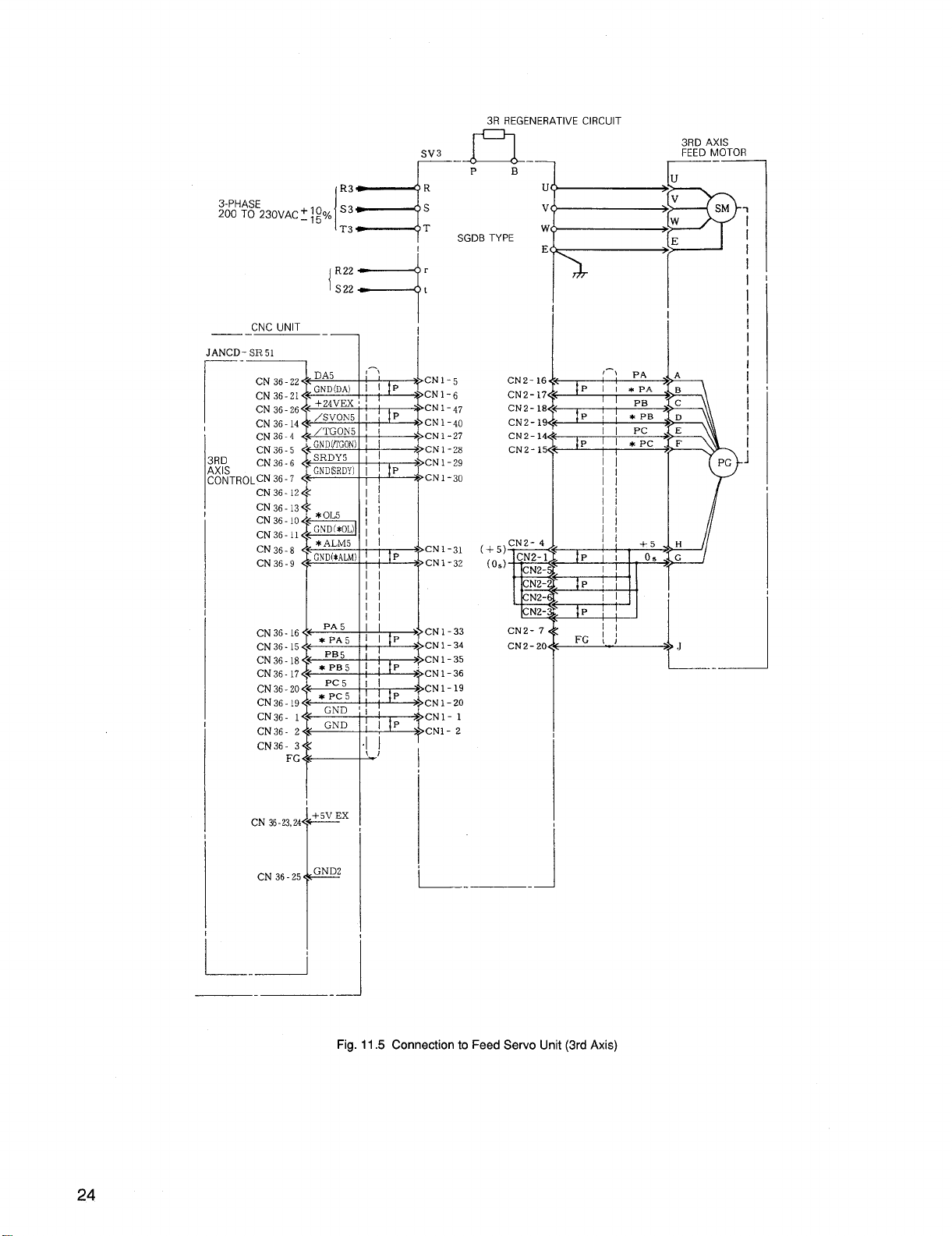
Fig. 11.5 Connection to Feed Servo Unit (3rd Axis)
I
I
‘L--- .–
Page 29
(2) For Machining Centers
3-PHASE
200 TO 230VAC : ;$Y,
RI S1 T1
war
I
NCM
II
R3 S3 T3
I
r
1 R REGENERATIVE CIRCUIT
%
SGDB TYPE
UA
v<)
W(1
E<
1ST AXIS
FEED MOTOR
~-
AU
.V
.J w
. .E
=-’
JANCD -SR 50.z
—-—
1ST
dxls
:ONTROL
.—
CN30 -22
CN30-21 < ~,~~;;
CN30-2
CN30-14 /’voN
CN30-4
CN30 -5
CN30-6
CN30 -7
CN30-1 <
cN30-1 <
cN30-1
cN30-1
CN30-8
CN30-9
CN30 -16
CN30-1
CN30-1 +~B~
CN30-17
CN30 2d
CN30. I
CN30. 1
CN30- 2
CN30. <
(
:N33.2i24&Ex
DA1
/TGON
i!i-
GND(tTGO!
SRDY1
GNDtSRDY
$
*OL1
GND(*OL
*ALIMI
GND[*AIA
/
,
*PA I
*PB1
4
*PC1
FC +——————
}
1
-/
PA I
Pc 1
GND
GND
]1
,[
II
II
II
k
II
!/
II
II
11P
=!
k::::
1P
~J
4
I
CN1-31 (+5)c~&
P
CN1-32
1
CN1-33
cN1-34
cN1-19
P
CN1-20
CN1- 1
CN1- 2
FG ‘
(0,)
CN2-:
CN2-2
CN2-(
CN2-:
E
CN2- 7.
CN2-20<
I
CN30-2 ‘ND2
L- .–
r
I
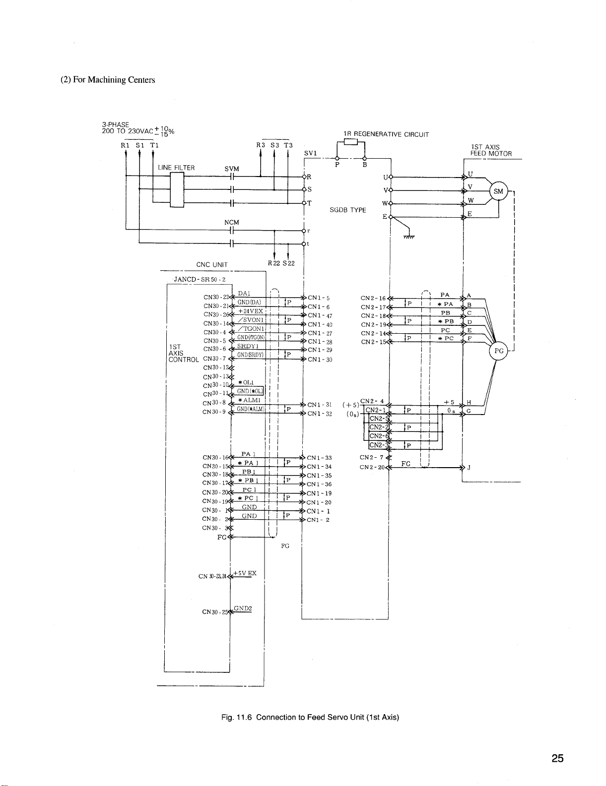
Fig. 11.6 Connection to Feed Servo Unit (1st Axis)
25
Page 30
3-PHASE
200 T0230VAC:\g% S3
I :=1
R22
{:
s 22
2P REGENERATIVE CIRCUIT
2ND AXIS
Sv 2
-n
P B-
R3
T3
R
s
T
—km
SGDB TYPE
FEED MOTOR
I
——
_CNC UNIT
LNCD - SR 50-2
—“~
CN31-12 <
CN31-13 <
CN31-10 &=
CN31.11 #llQl
cN31.8 &
CN31-9 _
1
i
+
-—
,
CN1-5 CN2-
4P }
CN1-6 CN2cNI-47 CN2-
P
~ CN1-27 CN2-
i=z
7
CN1 -40
CN1-28
CN1-29
P
CN1-30
+=/
iI& iii
*
+
CN1-19
CN1-20
CN1- 1
CN1- 2
/
CN2-
CN2-
cN2cN2-
—--J
CN 31-23,24=
CN31-25 ‘N’
\
L---
t-
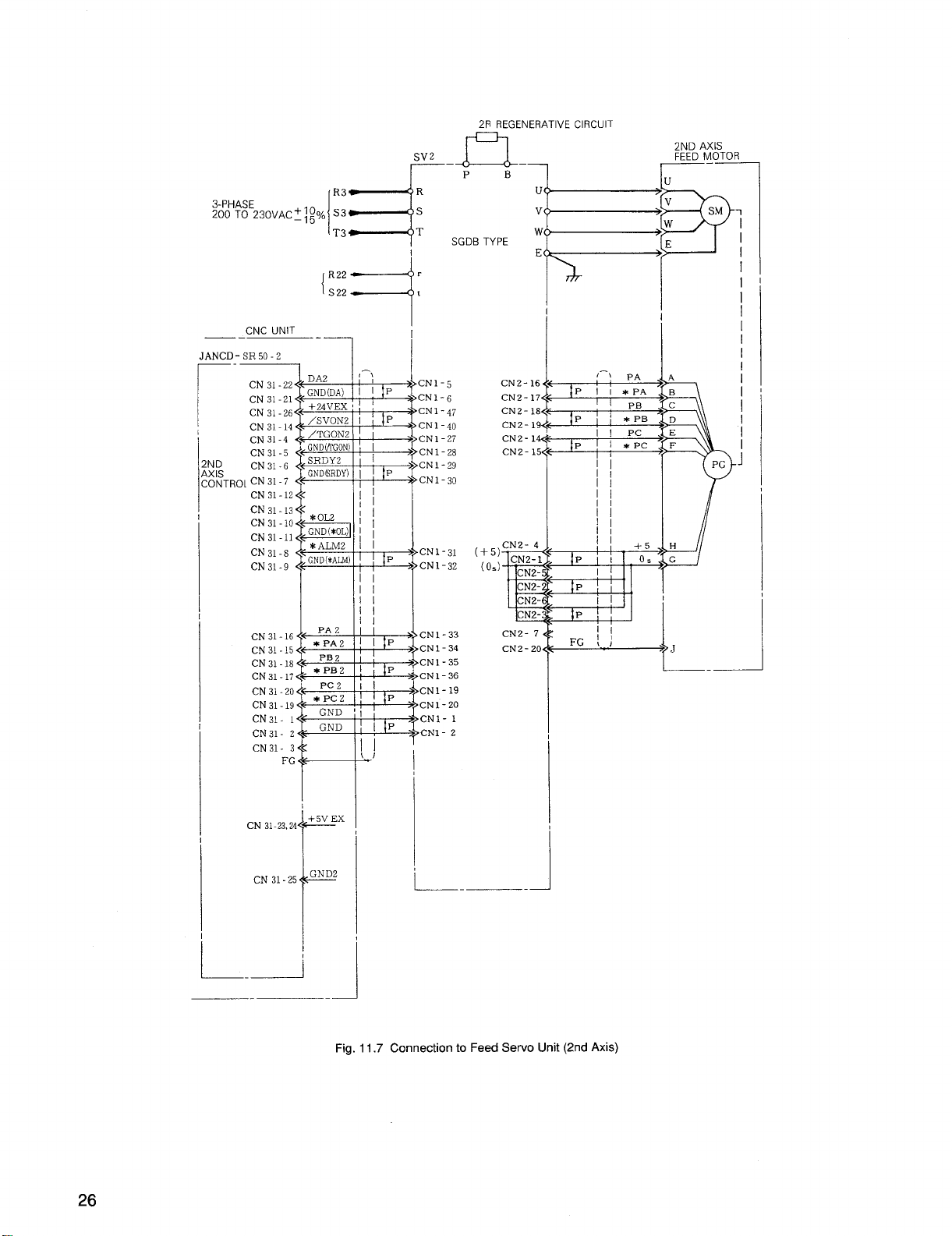
Fig. 11.7 Connection to Feed Servo Unit (2nd Axis)
Page 31

R3 R
;O~H%E230VAC~; @0 S3 s
E
T3
R22
s 22
s
CNC UNIT
—.
ANCD - SR 50-2
“-~
CN 33-$2
CN33-21 ~~;j
CN 33.26
CN33-14 ~G~
CN33-4
CN33-5
CN33-6
% GND(SRDY
:ONTROLCN 33-7 +——————
CN33-12~
CN 33-13<:*OL3
CN 33-10
CN33-11
cN33.8
CN33-9
CN 33-16
CN 33-15
CN 33-18
CN 33-17
CN33-20 i *:C33
CN 33-19
CN33. 1
CN33- 2
CN33- 3 <
-.
DA3
k
GNDtTGOh
SRDY3
f
GND(*OL;
*ALM3
GND($ALM
f
I
PA 3
*PA3
PB 3
*PB3
I
GND
GND
FG G——————
(-!
[1P
IF’
l-- CN1-27
1P
%
[!
~
il
II
II
[1
II
P
E/
II
II
II
II
II
11P
3+
E %::
k
g
3R REGENERATIVE CIRCUIT
SV3
n
I------P !3-1
T
SGDB TYPE
I
r
t
CN1-5
CNI-!5
CN1-47
CN1-40
CN1-28
CN1-29
CNI-30
=:-ii ~
CN2- 18
CN2-1
CN2-14
CN2-15
I
CN1-31 (
CN1-32
CN1-33
CN1-34
““’Ow-llJ
CN1-19
CN1-20
CN1- 1
CN1- 2
1
3RD AXIS
FEED MOTOR
r-—
u
v
w
E
u
v
w
E
1=1%
l-, pA
P
1~~
P
I“”b’
IIPCE
I *pc>F
II
1/
f!
II
1/
II
*PB D
—–
I
I
SM -I
~
PG
I
I
_.J
\
CN 32-23,24=Ex
1
CN32-25 ‘ND2
r
L- _
-1
-—
Fig. 11.8 Connection to Feed Servo Unit (3rd Axis)
Page 32

3-PHASE
200 TO 230VAC : ~:%
4R REGENERATIVE CIRCUIT
—
_CNC UNIT
JANCD - SR 51
~-~
CN
CN
CN
CN
CN
4TH
AXIS
CONTROL
CN
CN
CN
CN 36-12 <
cN36-13 f*oL5
CN 36.10
CN36-11
cN36.8
CN36-9
CN 36-16
CN 36-15
CN 36-18
CN 36-17
CN 36-20
Cii36-19
CN36- 1
CN36- 2
CN36- 3 <
R22
s 22
{+
-—
DA5
36-22
GND(DA)
36-21
+24VEI
36-26
36.14 /SVON!
/TGON
36-4
L
GNDVTGO}
36-5
SRDY5
36-6
GNDkWDY
36-7
i
$
GND(*OL
*ALM5
GND($ALh!
PA 5
*PA5
PB 5
*PB5
1
Pc 5
*PC5
GND
GND
FG ~
I
r
t
I
,-,
11P
1P
t--+---+ CN1-27
%
1P
T=
,1
,1
II
I
CN1-5
cN1-’f’
CN1-47
CN1-40
CN1-28
CN1-29
CN1-30
CN2-18
CN2-19
I
k%:; ‘::;c:~::c
II
[1
II
II
II
[[p
p
I ‘
p ? ::; ”J;
k
&&
:’ ~
[/
CN1-33 CN2- 7,
CN1-34
1
CN1-19
CN1-20
CN1- 1
CN1 - 2
E
CN2-20~
N2-’i
N2-6
N2-3
I
I
[
I
I
1
CN 36-23,24=Ex
CN36-25 ‘ND’
..J
I
{
I
I
L--- ._
k
Fig. 11.9 Connection to Feed Servo Unit (4 th Axis)
Page 33

(1) Connection and Motor Rotating Direction
Forward Connection
Reverse Connection
Direction of
Motor Rotation
if “+” moving
command is given.
E21
FLANGE
o
SURFACE
_ OF MOTOR
g
Ccw
The connection diagram shows forward connection.
Connect wires as shown below for reverse connection.
o
Cw
Line Filter Type
LF31O
LF320
LF330
LF340
Current per Phase of Input Power Supply
10A max
20A max
I
30A max
40A max
(4) Connection to Motor with Brake
SINGLE PHASE
100/200 VAC
SVMX
1=-- pUSHBUTTON
EMERGENcY
STOP
. Do not short-circuit output terminals 3 and 4.
. Tightly fasten terminal board screws.
.Protective devices are built-in. External protectors arenot needed.
. The contact making and breaking current for terminals 5 and 6
shallbe5 to 10times therated current of the brake to be used.
Use DC make-break contacts.
(2) Combination of Drive Unit and Regenerative Resistor
Servo Drive Type
CACR-
SR03SB
SR05SB
SRI OSB 70W–5flk
SRI 5SB
SR20SB
SR30SB
SR44SB
Regenerative Resistor installed
SeDaratelvTvi3eMO-
70W-50k (or 30SH, 300W 100Q)
70W-50k (or 30SH, 300W 100Q)
70W-50k
140W-25k
140W–25k*
140W-25k*
*Two registers connected in parallel,
(3) Line Filter Installation
(a) A line filter is installed to prevent radio interference by high
frequency generated by the servo drive unit.
(b) Select the appropriate filter as follows depending on the current
per phase of the drive unit input power supply.
Page 34

12. CONNECTION TO SPINDLE
DRIVE UNIT
12.1 CONNECTION TO EACH UNIT
(1) For Motor with Built-in PC
(a) For lathe
CNC UNIT
—
(b) For multi-axis lathe
JANCD-SR50-1
10226-52A2JL CN33
10220
-52A2JL CN32
1 GND 11
2 GND 12
3 GND 13
4 +5 VEX 14 PC3
5 +5 VEX 15 * PC3
6 +5 VEX 16 PA3
7 17 $ PA3
8 18 PB3
9 19 * PB3
10 20 FG
—
CNC UNIT
JAN CD-SR50-3
1022652A2J L
C33
1OI26-3OOOV
uR -
17
Ih”’’o”’ooov’
%FO1(G)
+~—
4
LIR~OM!Y(G)
Fig. 12.1
——
CN33
0126”3000vP
‘
CIMR-VM3
CN1 (1ST SPINDLE’
CN2
1 Ov 11 ccl
2 Ov 12 CA1l
3 Ov
4 +5V
!
5 + 5V 15 * Pcsl
6 + 5V 16
7 SG 17 * PAS1
8 THSAI 18 P8S1
9 THSE1 19 * PBS1
10 24V 20 FG
13 CA21
14 Pcs 1
PAS1
CN3
ID
MR2’JFO1(G)
C320
1
PG
SPINDLE
a
MOTOR
10220
52A2JL
1 GND 11
2 GND 12
3 GND 13
4 +5 VEX 14 PC3
5 +5 VEX 15 *PC3
: +5 VEX 16 PA3
8
9 19 *PB3
10 20 FG
H
-52A2JL CN%
10226
10220
52A2JL CN34
1
2 GND 12
3
4 +5 VEX 14 PC4
5 +5 VEX 15 * PC4
6 +5 VEX 16 PA4
.: 18 PB4
,9 19 * PB4
10
GND 11
GND 13
17 *PA3
18 PB3
17 * PA4
20 FG
CN32
0120 -3000vE
0126 -3000V
1P
0120 -3000VE
[
OR-
IFO1(G
CN1
U[
CN2
U[
4R-
>MOl(G
!R -
IFO1(G)
u
u
4R)MOl(G)
1 Ov 11 ccl
2 Ov 12 CA1l
3 Ov 13 CA21
4 +5V
5 +5V 15 * PCS1
6 +5v 16 PAS1
7 SG
8 THSA1 18 PBS1
9 THSB1 19 * PBS1
10 24v
m
1
CN 1
CN2 CN3
1 Ov
2 Ov
3 Ov 13CA22
4 +5V 14PCS2
5
6 +5v 16 PAS2
7 SG
8 THSA2 18 PBS2
9 TI+SB2 19 * PBS2
10 24V
m
I
Fig. 12.2
CIMR-VM3
CIMR-VM3
+5V
(1ST SPINDLE
CN3
14 PCS1
17 * PAS1
20 FG
(2ND SPINDLE
11CC2
12CA12
15 * PCS2
17 * P4S2
20 FG
IARiOFOl(G)
C340
10
!,lR
i3FOl(G)
1
L
PG
SPINDLE
a
MOTOR
PG
KI
Page 35

(c) For machining centers
CNC
UNIT
—
—
JAN CD-SR50-2
10226-52A2JL
10220
-52A2JL
1 GND 11
2 GND 12
3 GND 13
4 +5VEX 14 PC4
5 +5 VEX 15 *PC4
; +5 VEX 16 PA4
8
9
10
m
17 *PA4
18 PB4
19 *PB4
20 FG
—
(2) For Mortor with Separately Installed PC
(a) For lathe
CN35
CN34
C35
lD-
31263000L
C34
)120.3000VE
‘%
.—
I
MR -
EOFO1(G)
b
MR -
Fig. 12.3
CN1
[
CN2
1 Ov
[
2 Ov
3 Ov
4 +5V
5 +5V
6 +5v
7 SG
B THSA1 18 PBS1
9 THSB1 19 $ PBS1
10 24V 20 FG
H
CIMR-VM3
11 ccl
12 CA1l
13 CA21
14 Pcsl
15 * Pcsl
16 PAS1
17 *PAS I
(SPINDLE)
CN3
MR-
20F01(G)
L
PG
SPINDLE
c
MOTOR
CNC UNIT
JAN CD-SR50-1
10220-52A2J L
1 GND 11
2 GND 12
,3 GND 13
4 +5 VEX 14 PC3
,5 +5 VEX 15 * PC3
6 +5 VEX 16 PA3
,; 18 PB3
:0 20 FG
—
17 * PA3
19 * PB3
CN33
CN32
-~
IF
0126 -3000VE
lb
0120-3000V
—
C32-1
L.
r
L
)FO1(G)
fl[
[
Fig. 12.4
CN1
CN2
CIMR-VM3
(1ST SPINDLE)
C320
CN3
tiR?QFO1(G)
‘n
PG
E
SPINDLE PULSE
MS310BB-29S n ‘ENERATOR
G
!-J
u
Page 36

(b) For multi-axis lathe
CNC
UNIT
—
JAN CD-SR50-3
10226-52A2J L
10220-52A2JL
1 GND 11
2 GND 12
3 GND 13
4 +5 VEX 14 PC3
5 +5 VEX 15 *PC3
6 +5 VEX 16 PA3
7
8 18 PB3
9 19 *PB3
10
EEl
10226-52A2JL
10220-52A2J L
1 GND 11
2 GND 12
3 GND
4 +5 VEX :: PC4
5 +5 VEX 15 * PC4
6 + 5VEX 16 PA4
: 16 PB4
9
10
17 *PA3
20 FG
17 * PA4
19 * PB4
20 FG
CN33
CN32
CN35
CN34
~ ‘n
— —
10126-3OOOVE
C32-1
10120-3000V
I
n
IF-
101263OOOVE
C34-1
10120-3000V
CIMR-VM3
CN1
CN2
1 Ov Ill Ccl
2 Ov 121CA11
3 Ov 131CA21
4 +5V 14 Pcsl
5 +5V
6 + 5V 16 PAS1
7 SG
6 THSA1 18 PBS1
9 THSB1
10 24V 20 FG
L
dR.
i3FOl(G)
a[
CN1
CN2
1 Ov
[
2 Ov 12 CA12
3 Ov 13 CA22
4 +5V 14 PCS2
5 +5V
6 +5V 16 PAS2
7 SG 17 * PAS2
8 THSA2 16 PBS2
9 THSB2 19 * PBS2
10 24V 20 FG
❑
(1ST SPINDLE
15 * F’csl
17 * PAS1
19 * PBS1
CIMR-VM3
(2ND SPINDLE
11 CC2
15 * PCS2
C320
II
CN3
MR2UF01(G)
3
PG
SPISPl:~E
d
SPINDLE
PULSE
Ms310t3= GENERATOR
r~
C340
CN3
D
MR20F01(G)
‘1
PG
E
SPINDLE
MOTOR
~s3108B~ GENERATOR
SPINDLE PULSE
n
I
n
IL
I 1P
I
u
1
(c) For machining centers
CNC
32
UNIT
1022O-52A2JL CN34
— .
JAN CD-SR50-2
1 GND 11
2 GND ?,
3 GND 13
4 +5vEx 14 PC4
5 +5 VEX 15 *PC4
6 +5 VEX 16 PA4
7
8 18 PB4
9
10 20 FG
EEl
—
17 *PA4
19 *p134
I
—
I
10126-3OOOVE
I
C34-1 ,
B-
b
10120-3000V
ix
[
Fig. 12.6
CIMR-VM3
CNI
CN2
1 Ov
.2 Ov 12 CA1l
3 Ov 13 CA21
4 +5V
5 +5V
6 +5V
7 SG 17 * PAS1
s THSA1 1s PBS1
9 THSB1 19 * PBS1
10 24v 20 FG
11 ccl
14
15 * Pcsl
16 PAS1
(SPINDLE)
101
CN3
Pcsl
Ms3108= GENERATOR
C340
SPINDLE PULSE
G
Page 37

(3) Main Cercuit
200/220VAC, 50/60Hz
k
,
cl MR-vM3-i:; :;K
(1ST SPINDLE)
( )
COOLING FAN
( )
MOTOR
Y
Fig. 12.7 Connection to Main Circuit
33
Page 38

12.2 DETAILS OF CONNECTION
(1) For Motor with Built-in PG
(a) For lathe
UNIT
CNC
—.
J==l
CN33-22
CN3321
CN3?L8
c“” E@
-—
C)A3 .-..,
GND(DA) ~ ~
*ALM3
SPINDLE DRIVE UNIT
CIMR-VM3-HLI
CNI-3
CN1-4
‘Y
L
(1STSPINDLE)
Fig. 12.8 Connection to Motor
with Built-in PG (1st Spindle)
3T
CN32-16
CN32-17
CN32-18
CN 32-19
CN 32-14
CN32-15
CN3220
PA3 C-.., CN2-16
*PA3 \ \ P
i!
PB3 ,
* PB3 \
PC3 I I
*PC3 I i !
FG3
%%
I
j P CN2-19
P CN2.15
:. /’
I
CN2-17
CN2-18
CN2-14
34
Page 39

(b) For multi-axis lathe
CNC UNIT
—-
JANCD - SR50 -3
CN33-27
CN33-21
Ct433-8
CN33-9
=11
CN32-16 JPA3
CN32-17 ~
CN32-18
-+
CN32-19 ~
CN32-14
CN32-15 *PC3
==+-
CN32-20 FG
-–––t–
JANCD-SR50
CN35-22
CN35-21
CN35-8
CN35-9 —
=+:
CN34-16 I PA4
CN34-17
CN34-18
-–––+
CN32-19
CN34-14
CN34-15
CN 34-20
=/=
‘1
DA3~ ,-..>
GND(DA) ~
*ALM3
B&
I
kPA3
PB3
iP03
Pc 3
I
~
GND(DA)
*ALM3
6ND($A11
I
I
* PA4
PB4
*
PC4
*PC4
FG
I
I
-J
,-.,
::
!,
=
‘k’
H//H
INDLE DRIVE UNIT
CN1-3
] P:
CN1-4
7
:N2-16
:N2-17
:N2-18
:N2-I 9
:N2-14
:N2-I 5
H
SPINDLE DRIVE UNIT
\ clMR-vrd3-nil
F
I
I
I
I
CIMR-VM3-i’Xj
CN1-3
CN1-4
(1STSPINDLE)
(2NDSPINDLE)
CN3-16
CN3-17 =Ed=
CN3-18
CN3-19 *PB1,
CN3-14
CN3-”5 ZsIH!i=
CN3-4
CN3-1
CN3-5
CN3-2
CN3-6
CN3-3
i
cN3-8 l“ThtsAIl i
CN3-’ Ezlt=
CN3-7 ● SS “~’
CN3-16
CN3-17 *PA 2[ Pi
CN3-18 PB 2: ~
CN3-” zEzIEjn~
CN3-14
CN3-15 *PC 2: P’
CN3-4
CN3-1
CN3-5 +5V : ;
CN3-2
PB Ii {
z
Pcl~ :
+5V ; ]
w ! P:
+5V I ~
Ov ; P!
+5V f ;
Ov : P!
3
PA 2 :“”-’\
Pc 2: ,
=;
+5V : ;
Ov ~ P!
Ov ; P\
=
1“1
PI
3
.
4
—
5
i-~- PG
i-i---
—
2
—
9
—
[
&El
.10
r
.
3
P(3
1
2
9
Fig. 12.9 Connection to Motor with Built-in
PG (1st Spindle, 2nd Spindle)
I
35
Page 40

(c) For machining centers
UNIT
CNC
.— -—
JANCD-SR50-2
CN34-16
CN34-17
CN34-lS
CN32-19
CN34-14
CN34-15
CN34-20 FG “- ;
=/$=1
Fig. 12.10 Connection to Motor with Built-in
PG (Spindle)
SPINDLE DRIVE UNIT
PA4 :“-’.,
*PA4 ; ! P
PB4 [ ~
*PB4 ; ~ P CN2-19
PC4 { ;
*PC4 , ;
I
CN2-16
CN2-17
CN2-16
CN2-14
1P
CN2-15
I
I
CIMR-VM 3-Cii.i.
(SPINDLEI
=&&k
CN3-19 *PB 1: Pi
CN3-14 Pcl{ :
CN3-15 *PCl~ P’
CN3-4
CN3-1 Ov \ P!
CN3-5
CN3-2
CN3-6
CN3-3
CN3-8
43L
I
+--L--=’
xi
+5V : ;
+5V : ;
Ov \ P!
+5V : ;
Ov : P!
TMSAIi :
,m,
I
AC SPINDL
MOTOR
U/%SKA-[
r
1
2
9
11 TS
12
.
Pr3
Page 41

(2) For Motor with Separately Installed PG
(a) For lathe
—-_ _
JANCD SR50- 1
CNC UNIT
CN32-16
CN32-17
CN32-18
CN32-19
CN32-14
CN32-15
CN32-4
CN32-1
CN32-5
CN32-2
CN32-6
CN32-3
CN32-20
I I
I
PA3
)<
* PA3
/
PB3
>>
* PB3
/
PC3
>>
*PC3
/
\\
+5vEX
GND
+5VEX ;;
GND
+5V EX /;
GND
<
FG
I
SPINDLEPULSEGENERATOR
(1STSPINDLE)
I
,.-
, ‘,
: P;
I
:;
: P:
; P!
,
,,
II
!$
,;
1,
1,
;,
,4
1!
,!
1;
,1
!j
~ ?;
c P;
; PI
‘. ,
I
I
CNS-A
\
CNS-N
\
/
CNS-C
\
CNS-R
\
CNS-B Pc 1
\
CNS-P
\
//
E
PA 1
*PA1
PB 1
*PB1
*pcl
3 “ ‘‘;
—-
—
J
Fig. 12.11 Connection to Motor with
Separately Installed PG (1st Spindle)
37
Page 42

(b) For multi-axis lathe
— -— -
CNC UNIT
-’
CN32-16
CN32-17
CN32-18
CN32-19
CN32-14
CN32-15
CN 32-4
CN 32-1
CN 32-5
CN 2-2
CN32-6
CN32-3
CN32-20
SPINDLE PULSE GENERATOR
(1ST SPINDLE)
j~~ = :;
1,
*PC3
+5VEX ~1
//
Gt4D
/
+5VEX ~~
>:
GND ‘!. !
/
+5VEX 1:
>>
GND
/
,,
t,
,,
::
1,
l,,
,,
,,
(,
!,
r,
1,
II
t,
l;:
II
I
I P!
; P:
,
7
T
~
4)
A
\\
\
CNS-B
CNS-P
CNS-H +5
CNS-K OV
*PC1
IT;
I
I 1
CN34-16
CN34-17 —
CN%18
CN34-19
Phl,A-l A =Eh
“,. J-?-,7
CN34-15
=/: ,:
CN%4
CN34-1
CN34-5
CN34-2
CN%6
CN 14.2
-. .-! “
CN34-20
=/!D “‘;
/’
-.. I
t’A 4
*PA4
PB4 ~i
* PB4
PC4 ;!
*PC4
+5VEX 1;
GND
+5VEX ::
Gt4D
+5VEX ;;
GND
FG
,.-
,,
: P;
: P:
; P!
/ P;
‘ P;
~ Pt
‘. /
+
\.
/\
\
,-
\
\
//
E
SPINDLE PULSE GENERATOR
(2ND SPINDLE)
I 1
CNS-A
CNS-N
CNS-C
CNS-R
CNS-B
CNS-P
PA 2
*PA2
7
PC 2
*pc2
\
I
I
38
—- _ _
J
Fig. 12.12 Connection to Motor with Separately
Installed PG (1st Spindle, 2nd Spindle)
Page 43

(c) For machining centers
—._ _
CNC UNIT
JANCD-SRW-2
CN34-16
CN34-17
CN34-18
CN34-19
CN34-14
CN34-15
CN34-4
CN34-1
CN34-5 _
CN34-2
CN34-6
CN34-3
CN34-20
<
<
<
.
:
\
/
; *PB4
\
,
: *PC4
.
. +5vEX
.
.
.
I
PA4 /--’!
*PA4
PB4 f;
PC4 ;!
FG
I
: P!
: P:
:$P;
,
,,
1
!1
,;
1,
I
!1
1,
;1
II
);
,,
;I
./
SPINDLE PULSE GENERATOR
(1ST SPINDLE)
I
CNS-A
\
CNS-N
\
/
CNS-C PB 1
\
CNS-R
\
CNS-B
\
/
CNS-P
\
/
,
I
*PA1
*PB1
*pcl
PA
Pc 1
1
(PG)
1’
—-
._____l
Fig. 12.13 Connection to Motor with Separately
Installed PG (Spindle)
Page 44

12.3 CABLE SPECIFICATIONS
Table 12.1 Main Circuit Cable
Inverter Mod
CIMR-VM::
,
23P7
25P5
27P5
2011
200V
2015
2018 111
2022
2030
43P7
45P5
47P5
4011
400V
4015
4018
4022
4030
Terminal Name
Rated
c& y;:?
22
33
45
66
90
132
180
11
16
22
33
45
55
66
90
Size (mm2 ) ‘“te
600V Class
Fke-registant
Crosslinked
Polyethylene Cable
3.5 2.0
5.5 3.5
8.0 5.5
14.0 14.0
600V Class
Rubbet’-insulated
Cabtyre 400V Cable
3.5
5.5
8.0
14.0
Terminal Name and Screw Size
Inverter Terminal
Motor
Terminal
Input output
M5 M5 M4
MS M5 M5
M5 M5 M5
M8
M8 M8
30.0 22.0 22.0 M8 M8 M8
38.0
.22.0
50.0 30.0
28.0
50.0
M8 M8 M8
M8 M8 M8
50.0 M8 M8 M8
2.0 2.0 2.0 M5 M5 M4
2.0 2.0 2.0 M5 M5 M5
3.5 2.0
5.5
8.0 5.5
14.0 8.0
14.0 14.0
30.0 22.0
3.5
3.5
5.5
8.0
14.0
22.0 M8 M8 M8
30.0
M5 M5 M5
M8 M8
M8 M8 M8
M8 M8 M8
M8 M8 M8
M8
R, s, u, v, u, v,
T, E
W, E W, E
Note: Cable size isselected atambient temperature30~ when built with 3-core l-thread in the air.
The maxium allowable temperature of the conductor is 60~ for IV, VV and CT cables, and 110”C
for 600V fire-resistant crosslinked polyethylene cables.
Precautions on Cable Selection at High Ambient Temperature —>
When ambient temperature exceeds 30C, thecable allowable cument is reduced. Select thecable size in
accordance with the technical materials of the cable manufacturer based on rated current.
Table 12.2 Cooling Fan Motor Cable
Terminal Name and Screw Size
Inverter Cable
200V
400V
600V Class polyvinyl insulated wire,
Size 2mmZ
Inverter Terminal
Control Power
Input
M4
Cooling Fan
output
M4 M4
Motor Terminal
Page 45

13.
CONNECTION TO TAPE
13.1
CONNECTION TO EACH UNIT
CNC UNIT
13.2
DETAILS OF CONNECTION
JANCD- cPW
1
10220.52A2J L
JAN CD-CP50
1 SG1 11
2 DR1 12
3 ER1 13
4 Csl 14
5 RS1 15
6 RD1 16
7 SD1 17
8 18
9 19
10 FG
CN20-7 ,
CN20-6
x
m
CN20- 3
CN20- 2
CN20- 1
*
CN20
II
20 FG
Fig. 13.l Connection to Each Unit
......
SD
RD
,,
C20
1012O-3OOOVE
TAPE READER UNI1
T
200/220VAC,
50/60Hz
PTR
TAPE READER
DB-25P
---------- ,,.,,-
IAYt HtAUtK UNI I
MODEL 2801 E
POWER SUPPLY
200/220VAC,
50/60Hz
Note : Wire length between tape reader and main board should be 3 m max.
For using the cable exceeding 3 m, contact your YASKAWA representative.
J-
TRANSFORMER
;::~:ov
4
34128
m
TAPE HANDLER
1
2
E
MODEL 1402
MODEL 1500
—
—
Fig. 13.2 Connection to Tape Reader
Page 46

14. CONNECTION TO RS-232C INTERFACE
14.1 CONNECTION TO EACH UNIT
CNC UNIT
JAN CD-CP50
10220-52A2J L
1 SG1 11
2 DR1 12
3 ER1 13
4 Csl 14
5 RS1
6 RD1 16
7 SD1
6 DINO 18
9 024DI
10 FG ;; FG
w
14.2 DETAILS OF CONNECTION
15
17
CN20
C20
1012O-3OOOVE
Fig. 14.1 Connection to Each Unit
DB25S
RS-232C
INTERFACE
CNC UNIT
INTERFACE
CONNECTOR
—._____.-.—.-.—.—., I TO12f-3W0VE DB-25s
-. ——. —.—. -.— .-. —.
JANCD-CP59
,
I
Fig. 14.2 Connection to RS-232C
—
DE-25P
.
(;
>,
,, CN-3
>,
>
>j :
>’
:;
!:
\
>,’
+“;
CN-2
CN-4
CN-5
CN-20
CN-6
CN-7
TO OUTSIDE OF NC
42
Page 47

14.3 RS-232C INTERFACE
(5) Interconnection
(1) Transmission Mode
Start-stop synchronization: Each data bit is preceded by a start
signal, and followed by a stop signal.
A SINGLE START-STOP CHARACTER
r
DI D2 D3 D4 D5 D6 D7
OFF
Function OFF
Signal Condition
Logic
+
START
BIT
DO
DATA BIT
Table 14.1
Vo< -3V
Mark
1 0
STOP BIT
(1 OR 2 BITS)
00> +3V
ON
Space
(2) Codes Used
The following two types of codes areused, and are selectively
used by parameters (#6026D5, #6028D5).
. EIA codes or ISO codes
. EIA codes or 1S0 codes + control codes (DC 1- DC4)
To use control codes, the machine to be controlled must be
able to discriminate codes DC1 through DC4. Codes DC1 -
DC4 are as follows.
Table 14.2
Character
Dc ~ Tape reader
start
Tape reader
‘C2 punching
Tape reader o
DC3
stop
DC4
Tape punch
release
8 7 6 5 4 :;; 3 2 1
o
o
o
o
0
0 0
0
(3) Transmission Baud Rate
Transmission baud rates can be selected at any rate between 50
and 9600 bauds with parameters.
Refer to (7) in Par. 14.2.
(4) Cable Length
The permissible maximum cable length varies with the machine
to be controlled. Refer to the machine builder’s manual.
(Standard maximum cable length is 15 m.)
Table 14.3 RS-232C interface Connecting Cable(A)
NC (DB-25P)
Symbol
FG / Frame grounding
SD
RD Receiving data
RS Sending data
Cs Capable of sending
DR Data set ready 6
SG Signal grounding 7
ER Data terminal ready
Signal Name
Sending data
I
Connections
Pin
No.
/ 1 10—o I FG
2
3 RD
4 0 RS
5 G
\-o
0
\
20 IO BUSY
Ii
External
Equipment
Symbol
SD
Cs
DR
SG
NC outputs control codes DC 1- DC4 to start and stop the machine,
but the machine can not output control codes to control the NC.
However, when the machine under control is unable to process data
in time, it can control the CS signals of the NC to halt the data
outputting of the NC.
When CS signals of the NC are not used, short CS and RS as
shown Table 14.4.
Table 14.4 RS-232C Interface Connecting Cable (B)
0
0
External
Equipment
Symbol
SG
ER (OR
IO ARARM)
NC (DB-25P)
Symbol
FG I Frame grounding
SD I Sending data
RD Receiving data
RS
0
Cs Capable of sending
DR Data set ready 6
SG Signal grounding
ER
Signal Name
Sending data
Data terminal ready
Connections
Pin
~n
0—------ j FG
111
/21~/+SD
3 (3’”W RD
4 RS
5 Cs
A-) DR
7
0
20
bl
~Description of signals
FG: Safety grounding
SD : Transmission data (output)
RD : Received data (input)
‘1!’
START
I
I 1,,
I
~STOP
Page 48

RS: Request for sending (output) – When sending data, NC is
turned ON when starting transmission, and turned OFF when
transmission ends.
CS: For sending (input) –When this input signal is ON, NC can
send data. If the machine under control is unable to process
data in time, it can turn OFF this signal to interrupt the
transmission of data from NC within2 characters. When this
signal isnotused, connect lines asshown in Table 14.4.
SG: Signal grounding.
ER: Data terminal ready – Use this signal as a tape rewinding signal
if a tape reader is connected to an RS-232C interface. The tape
reader can be rewound if this signal is ON.
NOTE
Among the RS-232C interface signals, the following are
normally not used by the NC.
DR: Data set ready
ER: Data terminal ready
CD: Data receiving carrier detection
However, when “ 1” is set for parameter CHKDR (#6021 D4), a
DR (data set ready) interlock is added.
(6) Signal Exchange Timing
. When NC receives data.
Data can be received in the following sequence and timing.
(a) NC sends code DC1.
(b) At code DC1, the machine under control starts to send data to
NC.
(c) If the NC can not process data in time, it sends out code DC3.
(d) At code DC3, the machine stops sending data within 10
characters.
(e) NC again sends code DC1 after processing data.
(f) At code DC1, the machine sends out the data that succeeds the
previously sent one.
(g) Upon reading in the data, NC sends out code DC3.
(h) The machine stops sending data.
~RTPUT
SD
~uTpuT~
RD
INPUT
Cs
INPUT
* @ represents “rewide stop code”, which is the same as “%” of ISO.
DC1
DC3 DC1 7
J
1=”
Fig. 14.3
., ,.
,
10 CHARACTERS MAX
DC3
~
(a) NC sends out code DC2, and subsequently sends out data.
(b) If the machine under control can not process the data in time,
NC stops CS at no IO BUSY signal.
(c) Upon completion of the data processing by the machine, NC
turns on CS. NC sends out data that succeeds the previous one.
(d) Upon completion of data sending, NC sends out code DC4.
;?tTPUT
SD
OUTPUT ~
Cs
INPUT
~–
DC2
DC4
L
Fig. 14.4
NOTE
D.C1 and DC3 code from RD is not available when NC sends out data.
(7) Parameter Setting
When using RS-232C, set data transmission baud rates, stop bit
lengths, and control code sending specifications with the
parameters shown in Table 14.6.
(a) RS-232C interface port selection
Select the RS-232C interface port by setting #6003.
Table 14.5 RS-232C Interface Port Selection
Interface
RS-232C port 1 #6003Do
Note: The above bit is selected at parameter setting” 1”
Input output
#6003D4
(b) RS-232C interface port 1
Baud rate setting of RS-232C interface port 1 is shown in Table
14.6.
Table 14.6 Baud Rate Setting
~
110
150
~
z
200
>
2
300
2
m
600
~
m
1200
2400
4800
9600
0 0 1
0 0
0
0
0 1 1
0
1 0 0
1 0 0
1 0 1
1
1
1 1
1
0
0
0
1
0
1
o
1
0
1
0
When NC sends out data
NC sends out data in the following sequence and timing.
44
Page 49

14.3 RS-232C INTERFACE (Cent’d)
Stop bit length setting
“
# 6026 D4 for input 1: Sets stop bit at two bits.
# 6028 D4 for output O: Sets stop bit at one bit.
. Setting of control code sending
# 6026 D5 for input 1: Does not send control code.
# 6028 D5 for output O: Sends control code.
15. DIRECT-IN SIGNAL CONNECTION
SKIP
m
A—?—6
Oz. DI
DINo
CNC UNIT
TYPE JANCD-PC50
-—- _
CNIO-11, 12.13
CN1O-1.2,3,9
k
CN1O-8
—-
=
~ cN10-18
/DINo
15.1 CONNECTION TO EACH UNIT
CNC UNIT
‘1
1022O-52A2JL
JAN CD-CP50
CN1O
1
!
Clo
1012O.3OOOVE
lb
Ii
.~
Fig. 15.1
15.2 DETAILS OF CONNECTION
The following input signals require high-speed processing and are
connected to the PC board (type JANCD-PC50), instead of generalpurpose 1/0 boards.
These signals are processed directly by the NC main processing
unit without coursing through the PC.
DINO: Skip input
DIRECT
IN
Fig. 15.2 Direct-in Signal
Connection Using
OV Common
—-
—.
+24 VDI
F
FG
CN1O-2O
L
I
I--- __
CNC UNIT
TYPE JANCD-PC50
—_ —__
CN1O-I1, 12,13
CN1O-I,2,3,9
—
Direct-in signal connection is shown in Fig, 15.1 and 15.2,
-—&—
SKIP
Fig. 15.3 Direct-in Signal
Connection Using
24V Common
4
—-
DIN O
/DIN O
-%
CN1O-I8
CN1O-8
:N1o-2o
45
Page 50

15.3 DETAILS OF SIGNALS
‘NPUT‘AvE’ORM~
SIGNAL
RECEIVED BY
NC
40@
Fig. 15.4 Time Chart
_ TIME
40#s
JANCD-PC50
(a) OV Common
CN1O-1-3,9 I
~
JANCD-PC50
CNIO-ll -13
J<
+ 24V
APPROX
8mA
/-)
I
(b) 24V Common
Fig. 15.5 110Circuit
Page 51

16.
CONNECTiON TO GENERAL-PURPOSE 1/0 SIGNALS
16.1
CONNECTION TO EACH UNIT
CNC UNIT
MRP-8F0’
-[
1/0 MODULE
JAN CD- FC81O
CNII FC861
FC880
MR-8RMD2
DETAILS OF
CNC UNIT
CPS (POWER SUPPLY)
172040.1
m
I
— —— —
CONNECTION
I
CN13-3
.. B“ i
CN13-4
JAN CD-PC50
~- I SH I
)1
1
I
CN02
D
%izm+l[
P
I
Fig. 16.1
172060-1
CN1l-1
CN1l-2
CN1l-3
CN13-1
CN13-4
CN13-3
CN13-5
CN13
CN7
172037-1
1/0 MOD~ll F
I
JANc D- Fc810/Fc860/Fc881
Fig. 16.2 GonneGticm tvGeneral-purpoae l(O~ignal
CN7
CN7
Page 52

16.3 CONNECTION
TO ADDITIONAL GENERAL-PURPOSE
1/0 SIGNALS
CNC UNIT
JANCD-PC50
MR-8RMA4
16.4 DETAILS OF
CN13
CONNECTION
1/0 MODULE NO. I
JAN CD- F~81 O/FC860/FC861
CN13
MRP-8FOI
P
1/0 MODULE NO 1
JANCD-FC81O
/FC860/FC861
;Nll CN12
[
MR-8RMD2
,.-----
1/0
MODULE NO.2
JANCD-FC81O
C130
/FC860/F:8&12
;Nll
HI
MR-8RMD2
C200
BE @2040.;N”
CN7&o---
1/0 MODULE NO.2
JANcD-Fc810/Fc860/Fc861
1/0 MODULE NO.3
C130
H[
C200
H[
-O-*
CN7
JANCD. FC81O
/Fc860/Fc861
;Nll
MR-8RMD2
;N13
CN7 +24V
—
Fig. 16.4 Connection to Additional General-purpose 1/0 Signal
CN7 0,4V
-1
CN7 +24V
CN7 OXV
l------
I
Page 53

Notes:
1. Up to 3 general-purpose 1/0 modules can be connected (when FC8 10 or F860 is used.)
2. It is necessary to terminate the final module since another general-pm-pose I/O module can be added.
<Example>
CNC UNIT
‘7
I
“W”r
1/0 MODULE
1/0 MODULE
+13 +q.
NO. I SETTING
TERMINATION (sw3)
ON/OFF
lo~J3
(ForConnectingto anothermodule)
3. Logic can be set to “ 1” by short-pin SW2 setting of an 1/0 module (FC8 10, FC860, FC861) when the input contact is “closed”
disregarding whether common OV or 24V is used.
INVERS (SW 2)
ON/OFF
-10
(ON)
ON/OFF
0 ~]
(OFF)
NO.2 SETTING
~EM::ATION (SW 3)
(Forterminal1/0module)
4. 1/0 port 1/0 addresses of an 1/0 module can be set by rotary switch (SW1 ).
Positions of TERMINATION, INVERS, and ADDRESS switches
.
1/0 MODULE (JANCD-FC810, FC860)
1
1
1/0 MODULE (JANCD-FC861 )
❑ •“~
mm
ml F@
TERMINATION
kLJ2__dcN7
❑ ‘w’ Q,cn
f %SRDDRESS -
mm EillzElg
1/0 MOOULE (JANCD-SP50)
o
z
o
s
u
D
o
r
1
1
Swl
‘EBB
wl
~ADDRESS
.
;
0
;
I
I
49
Page 54

17.
CONNECTION TO GENERAL-PURPOSE 1/0
17.1
CONNECTION TO EACH UNIT
1/0 MODULE
‘~
CN2
MR-20RMD2
MR-50RMD2 MRP-50F01
MR-50RMD2 MRP-50F01
1/0 MOOULE
‘~
CN3
CN4
P’
~n
lo!
i
C52
MRP-20F01
C53
C54
‘z:ik
:$:i=
CN5 C65
FRC2-C50S12-OL
CN6
FRC2-C50S12-OL FRC2-AA50-20S
D
FRC2-AA50-20S
C66
0
c!
FOR UNIT SIGNALS
D
FOR UNIT SIGNALS
n
1/0 MODULE
-~
(Use thscablewhenexternalpowerIS supplled1
--
-ux!E!Ji ~
CN2
FRC2-C50S12-OL FRC2-AA50-20S
UOMOOULE
Pn !
C72
FRC2-AA50-20S
I
FOR UNIT SIGNALS
FOR OPERATOR’S
PANEL
SIGNAL
Page 55

17.2 DETAILS OF CONNECTION
17.2.1 FC81O/FC860 MODULE
r===l r
+24V
Ov
L-
--l
TYPES JANCD-FC81 O, FC860
CONNECTOR iN4
,
I
‘~ ’33)
(19)
>>
1
(35)
I
(21)
> >
(36)
>>
> >
(22)
>)
PIN NO
(5)
(6)
1
J
t
1
1
J
ADDRESS BIT
NO.
#looo. o
#looo. 1
#looo. 2
?$1000. 3
#looo. 4
#looo. 5
#1000. 6
#looo. 7
#lool. o
#lool. 1
#lool. 2
NO
(7)
>>
(23)
(38)
‘ ‘h
,
I
~
1
1
o
.4
Notes :
1. This connection example shows +24 V common.
OV common is also available. Refer to Par. 18.3.2.1 1/0 Module Types
JANCD-FC8 10/FC860 for connection details.
2. The addresses are those for module No. 1. The address layouts for
modules Nos. 2 and 3 are the same as shown above starting with newer
addresses. Refer to Appendix B (3), Address Classification for details.
#lool. 3
#lool. 4
#lool. 5
#1001. 6
#lool. 7
Fig. 17.2 Connection to Address and Bit Nos.
#1000.0 to#1001.7 on FC81 O/FC860 Modules
Page 56

I_===l
+2
1-
v
--l
(
d
/
TYPES JANCD-FC81 O, FC860
COtiNECTOR CN4 -
r
1
PIN NO,
I
(39)
(9)
> >
I 1
I
J
.—
ADDRESS BIT
NO. NO
#loo2 o
*1 OO2. 1
/------+
> ‘ (25)
(40)
> >
(lo)
(26)
> >
‘ (41)
2 >
(11)
2>
> (27)
(42)
>
‘ (12)
> >
(43)
> >
(13)
>>
(44)
> >
#loo2. 2
I
it
+
1
#loo2 3
#loo2 4
I
#loo2. 5
t
#1002 6
1
#loo2. 7
#loo3. o
#loo3 1
1
#loo3 2
1
#loo3 3
1
I
#loo3. 4
#loo3 5
#1003 6
#loo3, 7
r
4 \
L I
52
Coh’131
J :::.)
o
2.
~.
Notes :
1. This connection example shows +24 V common.
OV common is also available. Refer to Par. 18.3.2.1, 1/0 Module Types
JANCD-FC810/FC860 for connection details.
2. The addresses are those for module No. 1. (#1002.O to #1003.7). The
address layouts for modules Nos. 2 and 3 are the same as shown above
starting with newer addresses.
Classification for details.
Fig. 17.3 Connection to Address and Bit Nos.
#1002.0 to #1003.7 on FC81 O/FC860 Modules
Refer to Appendix B (3), Address
Page 57

POWER SUPPLY
+24V
Ov
F__l
_.--/,
TYPES JANCD-FC81 O, FC860
—.
CONNECTORCN4
PIN NO
(15)
ADORESS81T
NO. NO
#loo4. o
(46)
(16)
(48)
_.--.J’.
r-----
Notes :
1.This connection example shows +24 V common.
O V common is also available. Refer to Par. 18.3.2.1, 1/0 Module Types
JANCD-FC810/FC860 for connection details.
2. The addresses are those for module No.1. (#1004.O to #1004.7). The address
layouts for modules Nos. 2 and 3 are the same as shown above starting with
newer addresses. Refer to Appendix B (3), Address Classification for details.
.
(1 To 3)
‘+
02.
COM 32
I
4
I
#loo4.1
#1004.2
#loo45
Fig. 17.4 Connection to Address and Bit Nos. #1004.0 to
#1004.7 on FC81 O/FC860 Modules
53
Page 58

TYPES JANCD-FC81 O, FC860
——-
CONNECTORCN5
L
Ov
+24V
J
-_----/,
PIN NO
(23)
(22)
(21)
(20)
(39)
(38)
(7)
(6)
(12)
(11)
(25)
(24)
(lo)
(40)
(9)
(8)
(4)
(1TO 3)
,
jl
+1
+]
cord40
1
1
1
1
t
I
I
1
I
t
.44DRESS BIT
NO.
#loo5 o
#loo5. 1
#loo5 2
#loo5 3
#loo5 4
#loo5. 5
#1005 6
#loo5 7
#1006. O
#1006. 1
#1006, 2
#1006 3
#1006. 4
#1006. 5
#1006, 6
#1006. 7
4?
o
..
Notes :
1. This connection example shows +24 V common.
OV common is also available. Refer to Par. 18.3.2.1, I/O Module Types
JANCD-FC810/FC860 for connection details.
2. The addresses are those for module No. 1. (#1005.O to #1006.7). The
address layouts for modules Nos. 2 and 3 are the same as shown above
starting with newer addresses. Refer to Appendix B (3), Address
Classification for details.
Fig. 17.5 Connection to Address and Bit Nos. #1005.0 to
#1006.7 on FC81 O/FC860 Modules
Page 59

TYPES JANCD-FC81 O, FC860
CONNECTOR ?N5
_--_.-/,
PIN NO.
(18)
(17)
.
.
\
.
.
.
(14)
.
.
.
,
(13)
.
(36) —
(35)
(34)
(33)
1
1 1
J
, ,
LJ——Ll —————
I 1
J 1
L I
1
Iv +
I [
I
ADDRESS BIT
NO. NO
#loo7. o
#loo7. 1
#loo7. 4
#loo7. 7
#1008. O
#1008. 1
#1008. 2
#1008. 3
——————+>( 41)
~ ?:~o
Notes :
1.This connection example shows +24 V common.
OVcommon is also available. Refer to Par. 18.3.2.1, I/O Module Types
JANCD-FC810/FC860 for connection details.
2. Theaddresses arethose formodule No.l. (#1007.Oto #1008.7). The address
layouts formodules Nos. 2and3 arethesame asshown above starting with
newer addresses. Refer to Appendix B (3), Address Classification for details.
Fig. 17.6 Connection to Address and Bit Nos. #1007.Oto
#1008.7 on FC81 O/FC860 Modules
(26)
~
—
#1003 6
1
#1008 7
1
COM41
o
2.
Page 60

POWER SUPPLY
r-
+-
v
-J
r
TVPF< lAN~n.FrFtlf? FCRW
!,, L., . .. UWUW . --, -,,---”
—-
CONNECTOR CN5
PIN NO.
(49)
.
/
(48)
.
/
[47)
.
/
(46)
.
/
(45)
.
/
(44)
.
/
(43)
.
/
(42)
[29)
.
/
(1 ‘rO 3)
,
,
,
I
)
,
COM 42
}
ADDRESS RI;
NO
#loo9. o
#loo9. 1
#loo9. 2
#loo9 3
#loo9. 4
#loo9. 5
#1009 6
#loo9. 7
Notes :
1. This connection example shows +24 V common.
O V common is also available. Refer to Par. 18.3.2.1, 1/0 Module Types
JANCD-FC810/FC860 for connection details.
2. The addresses are those for module No. 1. (#1009.O to #1009.7). The address
layouts for modules Nos. 2 and 4 are the same as shown above starting with
newer addresses. Refer to Appendix B (3), Address Classification for details.
Fig. 17.7 Connection to Address and Bit Nos.
#1009.0 to #1009.7 on FC81 O/FC860 Modules
56
Page 61

F
I Ov +
L
TYPES JANCD-FC81 O, FC860
CONNECTOR CN3
v
PIN NO
(39)
.
/
(9)
4]
(25)
/44DRESS BIT
NO.
#lolo o
#lolo. 1
#lolo 2
.
.
/
.
.
/
.
.
>>
>>
> >
>>
L-> >
(40)
(lo)
(26)
(41)
(11)
(12)
(43)
(13)
(44)
(14)
(45)
T r
1~ +
1
I
I
I
1 1
#lolo. 3
#lolo. 4
I
#lolo. 5
I
#1010. 6
1
#lolo. 7
#loll 2
#loll. 3
#loll 4
#loll. 5
#1011 6
#loll, 7
COM20
J :~,
0
.,
Notes :
1. This connection example shows +24 V common.
OV common is also available. Refer to Par. 18.3.2 .1,1/O Module Types
JANCD-FC8 10/FC860 for connection details.
2. Theaddresses wethose formodule No.l. (#lOIO.O to#lOll.7). The address
layouts for modules Nos. 2 and 3 are the same as shown above starting with
newer addresses. Refer to Appendix B (3), Address Classification for details.
Fig, 17.8 Connection to Address and Bit Nos.
#1010.O to #101 1.7 on FC810/FC860 Modules
Page 62

POWER SUPPLY
L_’_l
v
TYPES JANCD-FC81O, FC860
coNNEcioRcN3
r--
(46) - ~
>5
r--- ‘(29)
I
Notes :
1. This connection example shows +24 V common.
O V common is also available. Refer to Par. 18.3.2.1, 1/0 Module Types
JANCD-FC8 10/FC860 for connection details.
2. Theaddresses arethose formodule No.l. (#1012.0 to#lOl2.7). The address
layouts formodules Nos. 2and3are thesame asshown above starting with
newer addresses. Refer to Appendix B (3), Address Classification for details.
.l(l T04)
#lo12. 1
#lo12 2
#lo12. 3
#lo12 4
#lo12 5
#1012 6
#lo12. 7
Fig. 17.9 Connection to Address and Bit Nos.
#1012,0 to #1012.7 on FC810/FC860 Modules
Page 63

m
L
+24V I
-J
TYPES JANCD-FC81 O. FC860
CONNECTOR CN2
}
1
1
I
t
}
fi:DRESS BIT
NO.
#lo13. o
#lo13. 1
#lo13. 2
$$1013. 3
#lo13. 4
#lo13. 5
#1013 6
#lo13 7
PIN NO.
(1)
/
.
/
(14)
;
(2)
.
/
(8) —
,
(15)
/
(3)
.
,
(9)
,
(16)
T I
,
,
)
-II
r 1
r
L
.
.
(18)
COM10
02.
1. This connection example shows +24 V common.
O V common is also available. Refer to Par. 18.3.2.1, 1/0 Module Types
JANCD-FC8 10/FC860 for connection details.
2. The addresses are those for module No. 1. (#1013.O to #1013.7). The address
layouts for modules Nos. 2 and 3 are the same as shown above starting with
newer addresses. Refer to Appendix B (3), Address Classification for details.
Fig. 17.10 Connection to Address and Bit Nos.
#1013.O to #1013.7 on FC810/FC860 Modules
Page 64

-.,,--- ,. .,-- ----- .. . ..
I Y Yt> J,41NLU-FL!3 IU, KXbU
—-
.—— -
CONNECTOR CN1
-—
PIN NO
(28)
+24V Ov
=
#l loo. 1
#l loo. 2
#l loo. 3
-i r“
#l loo- 4
#lloo.5
#1100. 6
ttl loo. 7
#llol. o
#llol.1
#llol.2
#no l-3
#llol.4
#1101.5 (19)
,—_--+
I
+
I
I
-1 T
*I
t
\
,
(26)
(27)
(41)
(8)
(7)
(6)
(5)
(29)
(2.4)
(23)
(22)
(21)
(20)
#1101.6
#llol.7
—-
Note :
The addresses are those for module No. 1. (#1 100.0 to #1 101.7).
address layouts formodules Nos. 2and3 are the same as shown above
starting with newer addresses.
Classification for details.
1
+
0,4
Refer to Appendix B (3), Address
Fig. 17.11 Connection to Address and Bit Nos.
#1 100.0 to#1101.7 on FC810/FC860 Modules
(lo)
(9)
(1 TO 4)
a
Page 65

TYPES JANCD-FC81 O, FC860
ADDRESS BIT
NO, NO.
#llo2. o
#llo2. 1
#llo2.2
#llo2.3
#1102.4
#llo2.5
#1102.6
I
inn,?. rcm c1 ,m”l “ I
I
PIN NO, i
‘30)< K------
‘40)< ~
1
‘39)< ~
‘38)< ~
I
I
I
●
1
1
I
A
I
‘37)< ~
’36) ~
‘35)<~
‘34)<~
u
I
v
-1
—-
#1102.7
#llo3. o
#llo3. 1
#llo3.2
#llo3.3
#llo3.4
#llo3.5
#1103.6
#llo3.7
::;< ~
~_
I
I
-1 T
r
I
1
r
I
4
0.4
1
1
t
+
t
“8)< ~
‘17)< ~
‘16)4——+=—%
“’);~
(14)
/
)’
(13)
/
1’
‘12’<‘~
‘1’)<~
I
.---J
Note :
The addresses are those for module No. 1. (#1 102.0 to #1 103.7).
The
address layouts for modules Nos. 2 and 3 are the same as shown above
starting with newer addresses. Refer to Appendix B (3), Address
Classification for details.
Fig. 17.12 Connection to Address and Bit Nos.
#1 102.0 to#1103.7 on FC81 O/FC860 Modules
Page 66

TYPES JANCD-FC81 O. FC860 I nnl. ,rm 1. lmnl ,, I
—. -—
—,
CONNECTORCN1
r“vv. r! a“... ,
I
I
ADDRESS BIT
#llo4. o
#llo4. 1
#1104.2
#llo4.3
#1104.4
#llo4.5
#1104.6
81104.7
NO.
PIN NO.
I T
~ ~
1
<
r
,P
I
I
I
[
1
I
I
t “’){~
(32)1< ]
‘48)< ‘~
‘47)< ~
‘4’)< ‘=——=—0—
(45)
(43)
I
L
(1 TO 4)
O
0,4
I
Note :
The addresses are those for module No. 1. (#1 104.0 to #1 104.7). The
address layouts for modules Nos. 2 and 3 are the same as shown above
starting with newer addresses.
Refer to Appendix B (3), Address
Classification for details.
Fig. 17.13 Connection to Address and Bit Nos.
#1 104.0 to #1 104.7 on FC81 O/FC860 Modules
Page 67

fi~DRESS BIT
#llo5. o
#llo5. 1
#loo 5- 2
#no 5.3
#no 5.1
#no 5.5
#no 5-6
#no 5.7
NO.
{
t
~_—
C“NNECT:5$-=il
(20)
+<
-1
I
r
I
r
,
,
4
4t
rl
Ov
I
“)~ ~
“0)< ~
‘17)< ~
(5)
‘6’< ~
“2< ~
(7)
“8)~
J
Note :
Theaddresses arethose formodule No.l. (#l105.0 to#llO5.7). The
address layouts formodules Nos. 2 and3 are the same as shown above
starting with newer addresses.
Classification for details.
Fig. 17.14 Connection to Address and Bit Nos.
#1 105.0 to#1105.7 on FC81 O/FC860 Modules
Refer to Appendix B (3), Address
Page 68

TYPES JANCD-FC810, FC860
r
CON NECT6=]
I
,
~
I +24V
Ov
I
I
Note :
The addresses are those for module No. 1. (#1 106.0 to #1 107.7).
address layouts for modules Nos. 2 and 3 are the same as shown above
starting with newer addresses. Refer to Appendix B (3), Address
Classification for details.
Fig. 17.15 Connection to Address and Bit Nos.
#1 106.0 to#1107.7 on FC81 O/FC860 Modules
‘1‘04) ~
Page 69

TYPES JANCD-FC8T0, FC860
—.
“DRESS”-m----d-t
#llo9. o
CONNECTO;~
PIN NO. i
I
T
~
‘“)< ~
#llo9. 1
#llo9. z
#l Io9. 4
#llo9.7
*
I
{
r
,
1
1
I
,
‘48){~
““(~
‘4’)&——=—&
Note :
The addresses are those for module No. 1. (#1 108.0 to #1 109.7).
address layouts for modules Nos. 2 and 3 are the same as shown above
starting with newer addresses.
Refer to Appendix B (3), Address
Classification for details.
—
The
Fig. 17.16
Connection to Address and Bit Nos.
#1 108.0 to#1109.7 on FC81 O/FC860 Modules
Page 70

“YPES JANCD-FC81O, FC860
---@--l
—.
~:DRESS BIT
#lllo. o
NO
CONNECiOR CN6
1
PIN NO.
(31)
1
I
(26)
-1
#lllo.1
#lllo.2
(25)
(24)
{
#lllo.3
#lllo.4
#lllo.5
#lllo.6
#lllo.7
!
I
I 1
r
t
(23)
(22)
(21)
(20)
(19)
(32)
----- I
#lllo. o
#1111.1
+,
I
#1111.2
#1111.3 (37)
#1111.4
r
t
J
#1111.5
(39)
(38)
(36)
(35)
(40)
<
#1111.6
#1111.7
(34)
(33)
Note :
The addresses are those for module No.1. (#11
0.Oto#llll.7). The
address layouts formodules Nos. 2and3 arethe same as shown above
starting with newer addresses. Refer to Appendix B (3), Address
Classification for details.
Fig. 17.17 Connection to Address and Bit Nos.
#111 0.0 to#111 1.7 on FC81 O/FC860 Modules
Page 71

17.2,2 FC 861 MODULE
TYPE JANCD-861
—- .—
F==l !C”NNECT”RCN1
L-
+
L.-
‘~ ‘1)
PIN NO
1
1~=
(2) #looo. I
>
(3)
2 ‘>
(4)
> >
(5)
> >
(6)
> >
I
(7)
}
(8)
> >
(9)
> >
(10)
>
I
(11)
>5
(12)
> >
(13)
> >
(14)
> >
(15) —
—
1
I
1
}
1
1
1
MIDRESS BIT
#looo. o
#looo. 2
tilooo. 3
#looo. 4
#looo. 5
#looo. 6
#looo. 7
#lool. o
#lool. 1
#lool.
#lool. 3
#loo]. 4
#lool. 5
#1001. 6
NO
2
-—-/_: >(16)
COM 00
J ::4’::046
o
2.
I
—-
Notes :
1. This connection example shows +24 V common.
O V common is also available. Refer to Par. 18.3.2.2, 1/0 Module Types
JANCD-FC861 for connection details.
2. The addresses are those for module No. 1. (#1000.O to #1001.7). The address
layouts for modules Nos. 2 to 7 are the same as shown above starting with
newer addresses. Refer to Appendix B (3), Address Classification for details.
Fig. 17.18 Connection to Address and Bit Nos.
#1000.0 to #1 001.7 on FC861 Module
#lool. 7
Page 72

POWER SUPPLY
+24V
(
F
—
------+ >(’9)
~ —, ;(26)
Y ’18)
~ ‘43’0 46)
TYPE JANCD-861
CONNECTOR 6NI
T“-
PIN NO
I
(20)
> >
(21)
> >
(23)
2 >
(24)
>
(25)
>
+1
COM01
ADDRESS 81T
NO.
#lo Oz. o
}
#loo2. 1
#loo2. 2
I
#lo Oz. 3
}
#loo2. 4
#lo Oz. 5
t
#1002. 6
1
#loo2. 7
L
I
1
7
NO.
p
L. _
0,.
Notes :
1. This connection example shows +24 V common.
OV common is also available. Refer to par. 18.3.2.2 I/O Module Types
JANCD-FC861 for connection details.
2. Theaddresses arethose formodule No.l. (#1002 .0to#1002.7). The address
layouts formodules Nos. 2t07 arethe same as shown above starting with
newer addresses. Refer to Appendix B (3), Address Classification for details.
Fig. 17.19 Connection to Address and Bit Nos.
#1002.0 to #1002.7 on FC861 Module
_—
Page 73

F==l
10”,
L
v
J
TYPE JANCD-861
C0NNEc;ORCN2
~
J
}
ADDRESS BIT
NO
#loo3. o
#loo3. 1
#loo3. 2
#loo3. 3
NO.
PIN NO.
/
,(1)
/<
(2)
> >
(3)
>
,
(4) —
>>
1
t 1-
I
~
(5)
>5
>
(7)
>?
t u u
14——l.—l ————
> (9) —
I l— I
(10)
>
(11)
>
(12) —
>>
(---Y c0M02
———J——+ >(43T04’)
1~ +
r ,
1 1
r
T
~
/ [
4
1 I
1
1
1
#loo3. 4
#loo3. 5
#1003. 6
#loo4. o
#loo4. 1
#loo4. 2
#loo4. 3
I
,
o
.4
I
Notes :
1. This connection example shows +24 V common.
O V common is also available. Refer to Par. 18.3.2.2, 1/0 Module Types
JANCD-FC861 for connection details.
2. The addresses are those for module No. 1. (#1003.O to #1 104.7). The address
layouts for modules Nos. 2 to 7 are
newer addresses. Refer to Appendix B (3), Address Classification for details.
Fig. 17.20 Connection to Address and Bit NOS.
#1003.0 to #1 104.7 on FC861 Module
tbe same as shown above starting with
Page 74

POWER SUPPLY
r-
+24V
TYPE JANCO-861
rl-)NNFcToFicN2
I
PIN NO
(19)
.
,
(20)
.
[ I
1
#loo5. o
I
#loo5. 1
I
7
.
.
.
.
(24)
(25)
---/:
r
L
Notes :
1. This connection example shows +24 V common.
O V common is also available. Refer to Par. 18.3.2.2, 1/0 Module Types
JANCD-FC861 for connection details.
2. The addresses are those for module No. 1. (#1005.O to #1 105.7). The address
layouts for modules Nos. 2 to 7 are the same as shown above starting with
newer addresses. Refer to Appendix B (3), Address Classification for details.
(26)
(18) —
(43 TO 46)
.
I
COM 03
1
1
#1005. 5
}
#1005. 6
1
#loo5. 7
1
Fig. 17.21 Connection to Address and Bit Nos.
#1005.0 to #1 005.7 on FC861 Module
Page 75

TYPE JANCD-861
CONN;CTORCN3 -
-.
H
L-
r
1
PIN NO.
I
~ 7(’)
> (2)
> (3)
> (4)
> ‘ (5)
(6)
> >
> (7)
(8)
> s
(9)
2 >
(lo)
> >
>‘ (11)
(12)
>
ADDRESS
NO.
#loo6.
#1006.
,
+1
#1006.
}
#1006.
#1006.
#1006.
I
#1006.
#1006.
I
#loo?.
#loo7.
J
#loo7.
#loo7.
(13)
>
2 >
1 (15)
><
(14)
L--J
I
+
I ,,.1
r~ Co”o’
----L-+
Notes :
1. This connection example shows +24 V common.
O V common is also available. Refer to Par. 18.3.2.2, 1/0 Module Types
JANCD-FC861 for connection details.
2. The addresses are those for module No. 1. (#1006.O to #1007.7). The address
layouts for modules Nos. 2 to 7 are the same as shown above starting with
newer addresses. Refer to Appendix B (3), Address Classification for details.
>(43T04’)
I
o
2.
#loo7.
#loo7.
#loo7
Fig. 17.22 Connection to Address and Bit Nos,
#1006.0 to #1 007.7 on FC861 Module
Page 76

-.,-- ,..,,.- ,.,..
I YYt JAIINLIJ-BO I
—.
CONNECiOR CN1
1
PIN NO. !
POWER SUPPLY
+7.4V
-.
I
.
Ov
#llol.3
#llol.4
#llol.5
#llol.6
#llol.7
I
I
4
1
~’
4t
b
“x){~
‘40)<~
‘4’)< ~
“’){~
rJ=+———
Note :
The addresses are those formodule No.l-l. (#llOO.Oto #l101.7). The address
layouts for modules Nos. 2 to 7 are the same as shown above starting with newer
addresses. Refer to Appendix B(3), Address Classification for details.
Fig. 17.23 Connection to Address and Bit Nos.
#1 100.0 to#1101.7 on FC861 Module
Page 77

TYPE JANCD-861
.AADRESS 81T
#llo2. o
NO.
CONNEC:O=
PIN NO.;
(47 ‘< ~
(27 ‘< ~
I
+24V (
T
v
-1
#llo2. 1
#no 2.2
#1102.3
#1102.4
#1102.5
#11 OZ.6
#l Io3. o
#llo3.3
#no?, .4
tillo3. 5
~<~
A
‘29)< ~
r
4
t
I
I
r
t
1
1
-t
‘30)<~
‘3’) ~
’32) ~
’33) ~
‘35)1~
‘38)1~
‘3’){~
I ‘40){~
‘43 T046) ~
4
0.4
I
J
Note :
Theaddresses arethose formodule No.l-l. (#1102 .Oto#l 103.7). The address
layouts formodules Nos. 2t07are thesame asshown above starting with newer
addresses. Refer to Appendix B(3), Ad&ess Classification for details.
Fig. 17.24 Connection to Address and Bit Nos.
#1 102.0 to#1103.7 on FC861 Module
73
Page 78

TYPE JANCD-861
r
CONNECT~R~
PIN NO.
POWER SUPPLY
+24V Ov
Y Y
0,4
Note :
The addresses arethose formodule No.l-l. (#1104.O to#l105.7). The address
layouts for modules Nos. 2 to 7 are the same as shown above starting with newer
addresses. Refer to Appendix B(3), Address Classification for details.
Fig. 17.25 Connection to Address and Bit Nos
#1104.0to #1105.70n FC861 Module
I
Page 79

TYPE JANCD-861
r
fi:DRESS BIT
#1106. O
#1106. 1
#llo6. 2
NO.
—
CONNECTOR CN3
~-
1
(49), ,
POWER SUPPLY
+24V
.
Ov
“
#1106. 3
#1106.4
#1106.5
#no 6.6
#1106.7
I
Note :
The addresses are those for module No.1-l. (#1106.O to#l106.7). The address
layouts for modules Nos. 2 to 7 are the same as shown above starting with newer
addresses. Refer to Appendix B (3), Address Classification for details.
[
I
I
I
{
Fig. 17.26 Connection to Address and Bit Nos.
#1 106.0 to#1106.7 on FC861 Module
}
(39),/
(40),,
(41)
,
75
Page 80

17.2.3 SP 50 BOARD
—
~$$’
CONNECTION
EXAMPLE
TYPES JANCD-SP50-1 , SP50-2
I CONNECTOR CN4
I PIN NO.
+24V
—
#looo. o
(3)
> >
(4)
> >
(5)
>>
(6)
> >
1
(7)
> >
(8)
> >
(9)
> >
(lo)
> >
1
(11)
(12)
(13)
> >
(14)
> >
(15)
>>
—————’~ >(16)
—
I— +
#looo.
#looo. 2
#looo. 3
,
+1
,
#looo. 4
#looo. 5
#1000. 6
t
#looo. 7
}
#lool. o
#lool. 1
1
#lool. 2
#lool. 3
#loo I. 4
#lool. 5
#1001. 6
1
#lool. 7
1
1
76
+24V
7 COM30
,
L
Notes :
1. This connection example shows +24 V common.
O V common is also available. Refer to Par. 18.3.2.3, SP50 Board for
connection details.
2. The addresses are those for module No. 1-1. (#1000.O to #1001 .7). The address
layouts for modules Nos. 2 to 8 are the same as shown above starting with
newer addresses. Refer to Appendix B (3), Address Classification for details.
Fig. 17.27 Connection to Address and Bit Nos.
#1000.0 to #1 001.7 on SP50 Board
-.
Page 81

CONNECTION
EXAMPLE
+24V
Y I
4)
TYPES JANCD-SP50-I , SP50-2
I CONNECTORC~4
I
I
> >
>
PIN NO.
(20)
COM 30
AOORESS BIT
NO.
#lo Oz. o
t
#lo Oz. 1
1
#loo2. 2
-~
I
NO
}
1
1
1
t
#lo Oz. 3
#loo2. 4
#loo2. 5
#1002. 6
#loo2. 7
J
i~ ’26)
Notes :
>
(23)
> >
(24)
> >
(25)
> L
, >}(17.18) — ]COM30
L
(43 TO 46)
+-----l
L
,
02,
1. This connection example shows +24 V common.
O V common is also available. Refer to Par. 18.3.2.3, SP50 Board for
connection details.
2. Theaddresses aethose formodule No.l-l. (#1002.0 to#lOO2.7). The address
layouts formodules Nos. 2to 8 are the same as shown above starting with
newer addresses. Refer to Appendix B (3), Address Classification for details.
~
Fig. 17.28 Connection to Address and Bit Nos.
#1002.0 to #1 002.7 on SP50 Board
77
Page 82

TYPES JANCD-SP50-1 , SP50-2
CONNECTGRCN5
~&l;;K~lON
~] (47 TO 50) I
-../_
~ “)
r ,24, -
! PIN NO.
(2)
> >
(3)
> >
1
(4)
>>
(5)
> >
(6)
> >
(7)
>)
,
(8)
> >
(9)
>>
(lo)
> >
(11)
> >
,
>>
> >
1
(12)
(13)
1
[
t
}
I
I
}
.—
fDRESS BIT
#loo3. o
#loo3. 1
NO.
#loo3. 2
#loo3. 3
#loo3. 4
#loo3. 5
#1003. 6
#loo 3.7
#loo4. o
#loo4. 1
#loo4. 2
#loo4. 3
#loo4. 4
#loo4. 5
+24V
#1004. 6
-~
1 cord 30
#loo4. 7
Notes :
This connection example shows +24 V common.
1.
O V common is also available. Refer to Par. 18.3.2.3, SP50 Board for
connection details.
2. The addresses are those for module No. 1-1. (#1003.O to #1004.7). The address
layouts for modules Nos. 2 to 8 are the same as shown above starting with
newer addresses. Refer to Appendix B (3), Address Classification for details.
Fig. 17.29 Connection to Address and Bit Nos.
#1003.0 to #1004.7 on SP50 Board
Page 83

$)W;MZ;ION
v
—————’
/~ >(26)
F ‘(’’’18)
TYPES JANCD-SP50-1 , SP50-2
FIORCN5 - .
I
PIN NO.
(20) ~
>
(21)
;!
(22)
2 >
(23) —
>>
(24)
> >
I
(25)
>>
COM 30
{
COM 30
AODRESS BIT
NO.
1
1
}
1
1
#loo5. o
NO
#loo5. 1
#loo5. 2
#loo5. 3
#loo5. 4
#loo5. 5
#1005. 6
#loo5. 7
024
I
Notes :
1. This connection example shows +24 V common.
O V common is also available. Refer to Par. 18.3.2.3, SP50 Board for
connection details.
2. The addresses are those for module No. 1-1. (#1005.O to #1005.7). The address
layouts for modules Nos. 2 to 8 are the same as shown above starting with
newer addresses. Refer to Appendix B (3), Address Classification for details.
Fig. 17.30 Connection to Address and Bit Nos.
#1005.O to #1005.7 on SP50 Board
79
Page 84

TYPES JANCD-SP50-1 , SP50-2
&I&J~Fd/10N
mNtiEcT0RcN6 - - -
PIN NO.
‘
(47 TO 50)
ii
—-----~ >(1)
> (2)
(3)
> >
>‘ (4)
> (5)
> (6)
> (7)
(8)
> L
> (9)
(10)
2 >
(11)
> >
I
(12)
2 >
(13)
>>
(14)
> >
(15)
>?
,
—----’~ >(’6)
—
+24V
AODRESS
NO
#1006. O
BIT
NO.
1
#1006. 1
,
,
it
I
1
1
I
I
1
t
}
I
1
1
I
1
#1006. 2
#1006. 3
#1006. 4
#1006. 5
#1006. 6
#1006. 7
#loo7. o
#loo7. I
#1007.2
#loo 7.3
#loo7. 4
#loo7. 5
#1007.6
#loo 7.7
F ‘( ’7”8)
COM 30
Notes :
1. This connection example shows +24 V common.
OV common is also available. Refer to Par. 18.3.2.3, SP50 Board for
connection details.
2. Theaddresses arethose formodule No.l-l. (#1006.0 to#lOO7.7). The address
layouts for modules Nos. 2to 8 are the same as shown above starting with
newer addresses. Refer to Appendix B (3), Address Classification for details.
Fig. 17.31 Connection to Address and Bit Nos.
#1006.0 to #1007.7 on SP50 Board
Page 85

Page 86

TYPES JANCD-SP50-I , SP50-2
r
#llo2. 1
cONNEcyORCN5~
1
:;:; NN::ION
Ov
,
#llo2.2
I
#1102.3
I
I
I
#1102.4
#llo2. 5
I
#1102.6
#llo3.1
I
#1103.2
#llo3. 3
#llo3.4
#1103.6
#llo3.7
I
I
[
I
t
‘2”{~
(30)
‘32){~
“’){~
‘36){~
(39)
(42)
,
‘43’0”)——————J
d
024
Notes :
1. This connection example shows +24 V common.
O V common is also available. Refer to Par. 18.3.2.3, SP50 Board for
connection details.
2. The addresses are those for module No. 1-1. (#l 102.0 to #l 103.7). The address
layouts for modules Nos. 2 to 8 are the same as shown above starting with
newer addresses. Refer to Appendix B (3), Address Classification for details.
17.33 Connection to Address and Bit Nos
Fig.
#1 102.0 to#1103.7 on
SP50 Board
Page 87

TYPES JANCD-SP50-2
—-
cONNEcT”R_c”’ ~
1
&NW:~lON
J
o
tillot.1
#1104.2
#llo4.3
#llo4.4
#llo4. 5
#1104.6
#llo4.7
#llo5. o
#llo5. I
#llo5.2
#no 5.3
$1105.4
#no 5.5
#1105-6
#llo5.7
(20)
<
(21)
<
<
(23)
(24)
<
{
[
I
1
1
1
}
J
1
I
(25)
(26)
(27)
(28)
<
(29)
(30)
<
(31)
(32)
<
(33)
(
(34)
/
TO 46)
(43
/
\
Notes :
1. This connection example shows +24 V common.
O V common is also available. Refer to Par. 18.3.2.3, SP50 Board for
connection details.
2. The addresses are those for module No. 1-1. (#1 104.0to#1105.7). The address
layouts for modules Nos. 2 to 8 are the same as shown above starting with
newer addresses. Refer to Appendix B (3), Address Classification for details,
Fig. 17.34
Connection to Address and Bit Nos.
#1 104.0 to#1105.7 on SP50 Board
Page 88

TYPES .IANCWIO-7
— -—
fO/RESS ~1:
#1106. O
CONNECTO; CN6
+24V
T
#1106. 1
#1106. 2
#1106. 3
#1106. 4
#1106.5
#l Io6.6
#1106. 7
—-
Notes :
1. This connection example shows +24 V common.
O V common is also available. Refer to Par. 18.3.2.3, SP50 Board for
connection details.
2. The addresses are those for module No. 1-1. (#1 106.0to#1106.7). The address
layouts for modules Nos. 2 to 8 are the same as shown above starting with
newer addresses. Refer to Appendix B (3), Address Classification for details.
v
I
{
1 I
I
I
(43 TO 46)
—
-----@J
(36)
<
(37)
(38)
(39)
==a
(40)
<
(41)
(42)
84
Fig. 17.35 Connection to Address and Bit Nos.
#1 106.0 to#1106.7 on SP50 Board
Page 89

17.3 EXPLANATION OF GENERAL-PURPOSE
1/0 SIGNALS
17.3.1 l/O PORTS
(1) The YASNAC J50 contains the programmable controller system
(PC). External signals can deallocated toits I/O ports freely
when the machine manufacturer designs a built-in PC. For
details, refer to Instruction Manual for YASNAC J50 PC System
(SIE-C843-12.1).
NC
MAIN
PROCESSING
CNC UNIT
#1200 -
MACHINE
SEOUENCER
)
PANEL
I/o
*lloo -
#looo-
17.3.2 1/0 CIRCUITS OF 1/0 PORTS
17.3.2.1
(1) Input Circuits
(a) When the internal power
1/0 MODULE TYPE JANCD-FC810/FC860
OV common and 24 V common can be set by an external device
for the input circuit.
Internal power supply and external power supply can be used
for 24 V power supply.
supply is used.
T-T
<
#1300 -
I
Fig. 17,36 System Configuration
(2)
The general-purpose 1/0 ports are mounted on the 1/0 module
I
GNERALPURPOSE
1/0
y
PORTSET AOORESSSET
lW-J
types JANCD-FC8 10, FC860, FC861 and on the SP50 board of
the CNC operator’s panel.
The numbers of 1/0 points of these modules are shown in Table
17.1.
Table 17.1 Numbers of 1/0 Points of Modules
Module Type Input
JANCD-
Fc810/Fc860 112
FCS61
SP50-1 64 32
SP50-2 64
Notes :
1. YASNAC J50 needs one 1/0 board incorporated in a CNC operator’s panel
(SP50-1 or SP50-2). Therefore, up to 3 board (max. inputs: 512 points, max.
outputs: 344 points) can be connected when only FC 810/FC860 is added. Up to
7 boards (max. inputs: 512 points, max. outputs: 448 points) can be connected,
2. Each module can be used together with the other, However, an 1/0 mea number
must not be overlapped. (Refer to Appendix 2.) If any 1/0 area number is
overlapped, alarm No. 374 occurs m status chunges to the input disabled status.
3. In order to muke it possible to add more modules, it is necessary for each 1/0
module to terminate the fhal board,
Points
64
I
I 1
output
Points
96
56
56
Remarks
4
For machine panels
(3) Address Setting
The relationship between the address and connectors is
indicated in Table 18.1. (This table applies to port 1. If a
different port is used, address changes are required.
Table 17.2 Address and Connector
;.neral. purpose I/o
COM42
COM2 1
COM 10
:JANCD-FC861)
::; ~ COMOO
CN 1
COMOI
:~ ~ COM02
CN2
COM03
:~ 3 COM04
1
CN
CNI
CN2
CN2
CN3
CN3
CN3
1N64JOUT56
lrIput Output (JANCD- ,:;::::, ) (JANCD- ::8M )
#I 002
#loo3
#loo4
#1 005
#1006
v
#I 007
#l 008
#1 009
#lolo
#lo] 1
#1012 CN3
#1013
I CN5
CN6 1
#l loo CN4
#llol CN4
#llo2 CN5
#1103 CN5
#1 104 ICN6]
#1 105 ICN61
#1 I 06 icN6j
#1107 —
#1108 —
.
—
—
—
—
:~ ~ COM41
CN5
:: I COM20
CN2
CN1
CN 1
CN 1
CN 1
CN1
CN2
CN3
CN3
CN6
i
l,:HNE &“)+E
#1116 -
(b) When the external power supply is used.
Note :
“Common” in the input circuit (for example, COM1O, COM20, COM21...total
9) cuu be either “+24
points as mentioned in Par. 17.3 1/0 signal interface and can be selected
freely. Set by wiring on the cable side.
OV Common
I
ox
t----l
L-J
+24 V Common
Fig. 17,37 Internal Input Circuits
024
I
OV Common
l-.----+--
1+
0,,
L.d
+24 V Common
Fig. 17.38 External Input Circuits
V common”’or “O V common” for every 8 or 16 input
I
I
,
85
Page 90

17.3.2.1 1/0 MODULE TYPE JANCD-FC81 O/FC860 (Cent’d)
(2) Output
(a) When the internal power supply is used.
Circuits
An noncontact wity polarity is used for outputs. Current under
operation must be 60 mA max (per circuit).
Internal power supply and external power supply can be used
for 24 V power supply.
CN7-1
r
I
+ 24V ~
CN7-2
O.rl
$==
+70v ;
1
I
24EX
+
LOAD
—
I
L-–O:~~
Fig. 17.39 Internal Output Circuit
(a) When the Internal power supply is used.
CNINT _ –
~—1 +24V -
E
~ 10.2mA
e
F
I
RV
o,,
“t-
7
O V Common
— —
I
24V
O,<v
I
CPS
–18 FB
1
(b) When the external power supply is used.
~OWER sup;LU
r-”t!~-?
I
024
0,+
r
—-—-d
Fig. 17.40 External Output Circuit
Notes :
1. All 96 output points are transistor source driver outputs, The current when ON
should be maximum 60 mA per circuit.
2. Every 8 points out of 96 outputs can be connected to some external power
supplies.
3.When tilving to LEDs with internal power supply, the current of all the 1/0
circuits should be 3.5 A max.
17.3.2.2
(1) Input Circuits
1/0 MODULE TYPE JANCD-FC861
O V common and +24 V common can be set by an external
device for the input circuit.
Internal power supply and external power supply can be used
for 24 V power supply. When internal power supply is used.
mount power supply selection connector on CNINT. When
external power supply is used, mount power supply selection
connector on CNINT.
‘b-–-l
+24 V Common
Fig. 17.41 Internal Input Circuits
(b) When the external power supply is used.
FER;Um cNExT
~ov
Note :
“Common” in the input circuit (for example, COM 10, COM20, COM2 1...total
9) can be either “+24 V common” or “O V common” for every 8 or 16 input
points as mentioned in Par, 17.3 1/0 signal interface and can be selected
freely. Set by wiring on the cable side.
+ 24V
L
%.2mA
w
Fig. 17.42 External Input Circuits
~y~l-+24V -
I
COM
COM
L
+24 V Common
‘1
RV
I
—
— -1
Page 91

(2) Output Circuits
A nonncontact with polarity is used for outputs. Current under
operation must be at most 60 mA (per circuit).
Internal power supply and external power supply can be used
for 24 V power supply.
(a) When the internal power supply is used,
~.—–
I
+ 24V
Jp
CNINT
+ ox
17.3.2.3 SP50 BOARD (TYPE JANCD-SP50)
(1) Input Circuits
r
COM
C
(+ ‘v
5.lmA
L
F
~-
0 V Common
0%
—
—
+ 24V
—
I
I
L-–-J
Fig. 17.43 Internal Output Circuit
(b) When the external power supply is used.
Notes :
All 56 output points are polarized contactless (transistorized source
1.
driver) outputs. The current whenON shouldbe maximum
60 mA per circuit.
2. Whendriving the LEDs with internal power supply, the current of all
the 1/0 circuits shouldbe max. 3.5 A.
— —
—
__-..-!
—
CNEXT I
7
CN 15-3
Fig, 17.44 External Output Circuit
POtiER suEP~
+24V OV
I
r–-
g
5.lmA
~ 1+
+ 24”
RV
k
0.
h
I
(2) Output Circuits (with Internal Power Supply)
I
L–_–––––
V Common
+24
Fig. 17.45 Input Circuits
SP50 BOARD
‘-=1
TI
I
t
1
L-—z-JJ’
Ov
+’
0,4
2+
—
Fig. 17.46 Output Circuit
Note :
A noncontact with polarity is used for 56 outputs,
Current under operation must beat most 60 mA (per circuit).
Page 92

17.3.3 POWER SUPPLY FOR 1/0 SIGNALS
(1) Internal power Sunpply
Internal power supply +24 V for 1/0 signals should be provided
by the machine tool builder. If internal power supply is used,
calculate the load current according to 1/0 points and confirm
that the current is within the allowable current value since there
is a current capacity limit according to 1/0 ON points.
The allowable current capacity of the internal power supply is 1.5A.
● Unit consumed current (When internal power supply is used) :0.1
A
● Panel 1/0 JANCD-SP50- 1, SP50-2 consumed current (When
internal power is used)
Input current (l-point) :5.1 mA (at ON)
Output current (1-point)
(differs from load.)
● General-purpose 1/0 signal 1/0 module JANCD-FC8 10, FC860,
FC861 consumed current
Input current (l-point)
Output current (l-point)
(differs from load.)
(Example of Calculation)
When JANCD-SP50-1 All 1/0 output are ON with LED load
(2.7kQ):
5.1 mAx64=326.4 mA (JANCD-SP50- 1 imput comsumed
current)
24 V/2.7 kx32=28.4 mA (JANCD-SP50- 1 output comsumed
current)
1500 mA-326 mA-284 mA-100 mA=790 mA (possible supply
current)
If the internal power supply is connectedtoJANCD-FC810 under
these conditions, overcurrent alarm of the internal power supply
(CPS18F) occurs to the input ON of 77 points or above.
790 mA/10.2 mA=77 points
:60 mA max
:10.2 mA (at ON)
:60 mA max
(2) Specifications of External Power Supply
Voltage
Ripple
:24 VDC t5%
:1070 (P-P)
Provide external supply with the above.
Page 93

18. CABLES
18.1 LIST OF CABLES
The interface cable are furnished with or without connectors.
Those cables shown in Table 18.1 are available.
If the machine builder is supplying the cables, prepare
equivalent cables based on the cable specifications.
Cable N CableTy
Table 18.1 List of Cables
Configuration
Connector Cable Type
.
CABLE-CL: ““~~
L
L
Cable Length
0.5. ~. L=5m
Cable Type
Remarks
Type 1012O-3OOOVE
Type 1032O-52AO-OO8 Type 1032O-52AO-OO8
(
UL 20276 AWG 28 x 10pairs
(Characteristic impedance: 120!2)
Type 1012O-3OOOVE
Type 10320-52A0-008 Type MR-20L
(
UL 20276 AWG 28 x 10pairs
Type 10126-3OOOVE
Type 10326-52AO-OO8 Type 1035O-52AO-OO8
(
UL 20276 AWG 28 x 13 pairs
Type 10126-3OOOVE
Type 1032O-52AO-OO8Type MR-50L
(
Type 1OI2O-3OOOVE
)(
Type MRE-20M01(G)
)(
Type 10156-3OOOVE
)(
Type MRF-50F01
)(
)
)
)
)
1/0
CRT panel signal
Spindle drive
unit feed back
Servo drive unit
Spindle drive unit
UL 20276 AWG 28 x 13pairs
Type 10126-3OOOVE
Type 10326-52AO-OO8 Type MS3057-12A
(
Type 10120-3000VE
Type 1032O-52AO-OO8Type MS3057-12A
(
UL 20276 AWG 28 x 10 pairs
Type 1012O-3OOOVE
Type 1032O-52AO-OO8
(
UL 20276 AWG 28 x 10 pairs
Type MS3108B2O-29S
)(
Type MS3108B2O-29S
)(
)
)
)
, Mamplifier
Servomotor
Optical encoder
Spindle optical encoder
Manual pulse generator
CABLE-JK.’”:
LGF-011-100
89
Page 94

Cable No.
2able Type
Table 18.1 List of Cables (Cent’d)
Configuration
Type 1-178288-5
Type 172026-1
Remarks
1/0 Power supply
Type 172026-1
Type 172026-1
1/0 Power supply
Type VCT DE 8402398
2mm2x5 cores
Connector: 10120-3000VE
1032O-52AO-OO8
*
Cable
:UL 20276 AWG 28x1Ocores
Direct-IN
Closing sequence
RS-232C interface
(Tape reader unit)
Connector :MRP-50F01
MR-50L
*
Cable
:KQVV-SB DE 8400095
1/0 (FC81O,FC861)
0.2 mm’x 50 cores
Connector: MRP-20F01
*
Cable
: KQVV DE 6428673
MR-20L
1/0 (FC810)
0.2 mm’X20 cores
Connector: 172025-1
*
Cable
: VCT D: 8402398
AC power supply
0.2 mm x 5 cores
)(
Type MRP-8F01
Type MR-8L
)
Type MRP-8F01
Type MR-8L
(
1/0
(
*
*Conector andcable are separately provided
KEV SB 0.2x 1core
(Characteristic impedance: 120C2)
Type MRP-20F01(G) TypeMS3108B2O-29S
Type MR-20L
Type MR3057-12A
)(
KQVV-SB DE 8400093
0.2 m: X 10 pairs
Connector :FRC2-AA50-20S
Cable
: B-50S61.OM
Connector :FRC2-AA20-20S
Cable
:B-20S 60.OM
)
Spindle optical encoder
connection
1/0 (FC860, FC861, SP50)
1/0 (FC860)
Page 95

18.2 SPECIFICATIONS OF CABLE
(1) Cable Dwg. No. DE8400093 (Type KQVV-SB, 0.2 mm’ x 10
pairs)
Table 18.2
No. of Pairs
Material
Conductor
P
Winding
Shield
Sheath
Material and Color
Thickness
Finished Cable Diameter
Armrox.Mass
Table 18,3 Characteristics
Max. ConductionResistance (20V)
Min. Insulation Resistance (20V) Mfl.km 50
Withstand Voltage VAC/min I 1000
Continuous Operation Temperature Range
Construction
mm
mm
k~ikm
10
Tinned annealed copper
stranded wire
0.2
16/0.12
0.55
Cross-linked vinyl
0.3
Paper tape lap winding
Pitch: 18,22,25, 32
T]rrnedannealed copper
stranded wire
Vinyl, black
1.2
10.0
130
fVkml 113
~ -30 to +60
(2) Cable Dwg. No. DE8400095 (Type KQVV-SB, 0.2 mm’x 50
cores)
Table 18,4 Construction
No. of CableCores
Material
Nominal Sectional
Conductor
Area
No. of Conductors
uer mm
Dimensions
Insulation
Material Cross-linked vinyl
Thickness
Winding
Sheath
Material and Color
Thickness
Finished Cable Diameter
Approx. Mass
Table 18,5 Characteristics
kg/cm 230
Max. ConductionResistance (20C)
Min. Insulation Resistance (20C)
Withstand Voltage
Continuous Operation Temperature Range
50
Tinned annealed- copper
stranded wire
0.2
mmz
16/0.12
mm
0.55
0.3
mm
Paper tape lap winding
Soft Vinyl, black
mm
1.2
mm I Approx. 13
Wkrnl 113
Mfl.kml 50
VAC/min 1000
c -30 to +60
. Details of Cable DWG.
No. DE8400095
. Layout of 10 Pairs
Note :
Drain wires of 0.2mm’are
provided inside tinned annealedcopper stranded wire.
Pair No. I
6 I Blue/Brown
‘1
I
,
8 Green/Brown
*
Colors
Yellow/Brown
(3) Cable Dwg. No. DE6428673 (Type KQVV, 0.2 mm’ x 20 cores)
Table 18.6 Construction
No. of CableCores I 20
Tinned annealed copper
stranded wire
0.2
mmz
16/0.12
mm
Conductor
Material
Nominal Sectional
Area
No. of Conductors
uer mm
I Dimensions mm I 0.55
Insulation
Material
Thickness mm I 0.3
Cross-linkedvinyl
Winding Paper tape lap winding
Sheath
Material andColor
Thickness mm
Finished Cable Diameter mm
Soft Vinyl, black
I 1.2
8.0
Approx. Mass kg/cm ] 90
91
Page 96

Table 18.7 Characteristics
Max. ConductionResistance (20K2
Min. Insulation Resistance (20C)
Withstand Voltage
Continuous Operation Temperature Range
Details of Cable
No. DE6428673
.Q/kml
Mf2.km 50
VAC/min
r -30 to +60
113
1000
White
(4) Cable Dwg. No. DE8402398 (Type VCT, 2 mm’ x
Table 18.8 Construction
No. of Pairs
Material
Nominal Sectional
Conductor
Insulation
Sheath
Finished Cable Diameter mm
Max. Conduction
Min. Insulation Resistance (20C)
Withstand Voltage
ContinuousOperation Temperature Range
~
I Thickness mm
Diameter
-
Table 18.9 Characteristics
Resistance (20’C)
5
Tinned annealedcopper
stranded wire
2.0
37/0.26
1.8
Insulation vinyl
0.8
mm
3.4
Right twisted
(outerdiameterappmx.9.2 mm)
Vinyl, block
Approx. 1.9
Armrox. 13.t)
Q/kml 10.2
Mi2.km 500rmore
VAC/min 3000
C Oto+60
5 cores)
. Details of Cable Dwg. No. DE8402398
Black
E
5X
Brown :~- white
.......0
.: ~:o.
... .
t
Yellow
Red
Q!!z’
92
VINYL SHEATH
/ INCLUSION
7
Page 97

18.3 LIST OF CONNECTORS
(1) CNC UNIT
Table 18.10 Connectors for CNC Unit
CNC Unit Type
CPS-18FB
JANCD-SR 50-1
JANCD-SR 50-2
JANCD-SR 50-3
JANCD-SR 51
JANCD-CP 50
JANCD-PC 50
JANCD-MM51
:onnecl
No.
CNI
CN2
CN3
CN30
CN31
CN32
CN33
CN30
CN31
CN33
CN34
CN35
CN30
CN31
CN32
CN33
CN34
CN35
CN36
CN20
CN1O
CN1l
CN12
CN13
Connector Type
for Board Side
172040-1 (5 pins)
172040-1 (5 pins)
172039-1 (7 pins)
10226-52A 2 JL (26piIIS)
10226-52A 2 JL (26piIIS)
10220-52A 2 JL (20piIIS)
10226-52A2 JL (26pins)
10226-52A 2 JL (26pins)
10226-52A 2JL (26pills)
10226-52A2JL (26pklS)
10226-52A 2 JL (26piIIS)
10226-52A 2 JL (26pinS)
10226-52A 2 JL (26pfi)
10226-52A 2 JL (26pkls)
10220-52A 2 JL (20piIIS)
10226-52A 2 JL (26pti)
10220-52A2JL(20pinS)
10226-52A 2 JL (26pfi)
10226-52A 2 JL (26piIIS)
10220-52A2JL (20pti)
10220-52A 2 JL (20pinS)
1022@52A2JL(20piIIS)
1022052A2 JL (20pti)
M&8RMA4(8pills)
Cable Side
ConnectorType
CaseType
ContactorTW
172026-1
172026-1
172025-1
10126-31XOVE(10126-&XDEL) 10326-52AO-(IX(10326-A2CM3)
10126XKXIVE(lo126-@XlEL) IO326-52AWMJ(1O32,WZXW3)
1012O3CCOVE(1012W5OX)EL)1032@52A04113(1032DA2OMD)
10126-3W13VE(10126-60XIEL) 10326-52AO4II3(1032bAXXM13)
lo126-mvE(lo12&aClm) 1037652 AWI38(10326-A2CQO3)
1012&3W13VJ3(10126-6tXKIlZL)
I01K3WK3VE( 10126-KKK3EQ 1032652 AOC@3(1032&.A2fIN3)
10?2652AO4II3 (1032&%M!-@ —
1012O-W33VE(1012CMXMIEL) 10320.52AWXkS(103XM2W.CO)
101263OXIVE(10126-6OXIEL) KLW52AWXB(1032&AXDCQ
101263(XY3VE(10126-61XQEL)
1032&52AC-W3(103%A2OXQ —
101263CQ3VE(1OI2MXI3EL)103M52AWXR(103%MO3.CO)
lo120-m VE(1012WXUIEL) 1032D52AWD3(1032&42#03)
lo12&3J3WlvE(lo126-f KiX)EL) 10326-52AC-(DS(10326-A2IXW3)
1012G3(HIVE(IO1XMWOEL)1032O-52AOJXB(1032M2CC-Q
10126-3UDVE(lo12&lX13EL)10326-52AC-W3(103Z%42XW3)
10126-30X)VE(10126-61XIJEL)
10326-52AWX13(KE2&AXDCO)—
10120-3(INVE(I012WKXK)EL) 103X3-52A(MMI(103XM2OXI3)
1012034XOVE(lo120-6fXOEL)1032O-52AO.(IX(1032W2IXMQ)
1012C-3C03VE(1O12Q6XX3EL)1032O-52ACKM(103XMXXKX3)
10120.3(KOVE(1012.W XD3EL)
W-8F01
connector is provided
No
1032(L52AC-WB(1O32C-A2CCW3)—
MR43L
170289-1
170289-1or
170289-1
—
—
—
—
—
—
—
—
—
—
—
—
—
—
—
—
MRP-F112
Manufacturer
AMP
3M
3M
3M
3M
3M
3M
3M
3M
HONDA
Note :
Connectors for the cable side are not attached to the cables.
The machhe builder must suppiyequivalent connectors.
Page 98

Connector Position
JZNC-JRK 00
JR 50
—
u
CPS-18FB
I YASNAC I
F
o
0
o
0
0
(2) CNC Operator’s Panel
CNC Panel Type
JANCD-SP 50-1
JANCD-SP 50-2
Note:
Connectorsfor the cable side are not attachedto the cables.
The machine builder must supply equivalent connectors.
Connector
No.
CN1
CN2
CN3
CN4
CN5
CN6
Connector Type
forBoardSide
1022O-62O2JL(20 pins)
1022O-62O2JL(20 pins)
1-178315-2 (5 pins)
FRc2-c50s12m (50pii)
FRC2<50S12-OS(50Pii)
FRC2.C50S124S(50pirrs)FRC2-AA 50-20
Fig. 18.1
Table 18.11 Connectors for CNC Operator’s Panel
ConnectorLayout(JZNC-JRKOO)
Connector Type
lo120-3030vE(lol~ f3L)
1012O-3W3VE(101XMCOOEL)
1-178288-5
FRC2-AA 50-20
FRC2-AA 50-20
1032O-52AOOT3(10326-AXKKJ3)
1032O-52AC4XB(103%-~)
Cable
CaseType
Side
ContactorType
—
—
175218-2
Manufacturer
3M
3M
AMP
DDK
DDK
DDK
Fig. 18.2
Connector Layout of CNC Operator’s Panel (Type JANCD-SP50-I, -2)
Page 99

(3) 1/0 Module Connector
Table 18.12 Connectors for 1/0 Module
1/0 Modeule Type
JANCD-FC81o
JANCD-FC860
JANCD-FC86I
Ionnect(
No.
CN1
CN2
CN3
CN4
CN5
CN6
CN1l
CN12
CN13
CN14
CN1
CN2
CN3
CN4
CN5
CN6
CN1l
CN12
CN13
CN14
CN1
CN2
CN3
CN1l
CN12
CN13
CN14
CN15
Connector Type
foR Board
Side
MR-50RMD2 (50pins)
MR-20RMD2 (20pins)
MR50 RMD 2 (50pins)
MR-50RMD2 (50pins)
MR-50RMD2 (50pins)
m-50 RMD 2 (50pins)
MR-8 RMA 4 (8 pins)
MR-8 RMA 4 (8 pins)
172040-1 (5 pins)
172040-1 (5 pins)
FRC2-C5QS12-OL(50pins
FRC2- 12-OL(~pitl$
ERC24XlS124)L(Wpti
FRC2JCXlS1243L(Xlpim
FRC2J-25CB124)L(50pti
FRC2-C50S12-OL(50pti
MR-8RMD 2 (8pins)
MR-8RMD 2 (8pins)
172037-1(5 pins)
172037-1(5 pins)
FRC2-C.X)S12-OL(5Q@
FRC24XlS12-OL(20pim
MR-50RMD 2 (50pins)
MR-8 RMA 2 (8 pins)
MR-8 RMA 2 (8pins)
172037-1(5 pins)
172037-1(5 pins)
1-178313-2(3 pins)
Connector Type
MRP-50F 01
MRP-20F 01
MRP-50F 01
MRP-50F 01
MRP-50F 01
MRP-50F 01
MRF-qF 01
MRP-qF 01
172026-1
172026-1
FRC2-AA 50-20S
FRC2-AA 20-20s
FRC2-AA 50-20S
FRC2-AA 50-20S
FRC2-AA 50-20S
FRC2-AA 50-20S
MRP-8F01
MRP-8F01
172026-1
172026-1
FRC2-AA 50-20S
FRC2-AA 20-20s
MRP-50F01
MRP-8F01
MRP-8F01
172060-1
172060-1
1-178288-3
Cable Side
MR-50L
MR-20L
MR-50L
MR-50L
MR-50L
MR-50L
MR-8L
MR-8L
MR-8L
MR-8L
MR-50L
MR-8L
MR-8L
CaseT~
~ontactorTypt
MRP-F112
MRP-F112
MRf-Fl 12
MRP-F112
MRF-F112
MRF-F112
MRP-F112
MRP-F112
170289-1
170289-1
MRP-F112
MRE-FI 12
170289-1
170289-1
MRP-F112
MRP-F112
MRP-F112
170289-1
170289-1
175217-2
tianufacturer
HONDA
HONDA
HONDA
HONDA
HONDA
HONDA
HONDA
HONDA
AMP
AMP
DDK
DDK
DDK
DDK
DDK
DDK
HONDA
HONDA
AMP
AMP
DDK
DDK
HONDA
HONDA
HONDA
AMP
AMP
AMP
Note :
Connectors for the cable side are not attached tothe cables.
The machinebuilder must supply equivalent connectors.
Page 100

Fig. 18.3 Connector Layout of 1/0 Module (JANCD-FC81 O)
+
-+
Fig. 16.4 Connector Layout of 1/0 Module (JANCD-FC860)
+
%?!%! “ma~
Fig. 18.5 Connector Layout ofl/OModule (JANCD-FC861)
TYPE JANCD-FC860
CN13 CN14
TYPE JANCD-FC861
CN15
1
n
u
FG
~~ +’-
<:
A.? ,
 Loading...