

Page 1
GPD 515/G5 Modbus
®
RTU
Technical Manual
Page 2

Technical References
Refer to the following publications for further information about the GPD 515/G5:
• GPD 515/G5 Technical Manual
Publication TM 4515
• GPD 515/G5 RS-232C/485 Interface Card Installation Sheet
Publication 02Y00025-0401
Refer to the following Modicon publication for technical information on Modbus RTU protocol:
• Modicon Modbus Protocol Reference Guide
Publication PI-MBUS-300 Rev. D
Technical Support
Technical Support Center-
Provide telephone assistance related to installation, start-up, programming, and
troubleshooting drives and communication products. For technical phone support
call 1-800-541-0939.
Technical References / Technical Support i
Page 3

CONTENTS
Technical References / Technical Support i
Contents 1
Chapter 1 GPD 515/G5 and Serial Communication 1-1
Introduction to GPD 515 Modbus RTU Communication 1-2
Standard RS-232D Serial Communication 1-2
The RS-232D to RS-485 Converter Board 1-3
Figure 1-1. The CM085 Board 1-3
Chapter 2 RS-232D Serial Communication 2-1
RS-232D Serial Communication 2-2
Figure 2-1. RS-232D Pin-out at 6CN Connector 2-2
Chapter 3 Installation of CM085 Board 3-1
Installation Procedure 3-2
Figure 3-1. Position of the CM085 Board
on the GPD 515 Drive 3-2
Chapter 4 Wiring of the CM085 Board 4-1
Connection of Multiple Drives 4-2
Figure 4-1. Interconnection Diagram 4-2
Wiring Instructions 4-3
Figure 4-2. Twisted Shielded Wire Termination 4-3
Table 4-1. Functions of Terminal Block TC1 4-3
Table 4-2. Applicable Wire Sizes for Terminal Block TC1 4-3
Terminating Resistors 4-4
Figure 4-3. SW1 Location on the CM085 Board 4-4
Chapter 5 Setting GPD 515 Parameters for Communication 5-1
Run/Stop and Frequency Selection 5-2
Communication Set up Parameters 5-3
“ENTER” Command 5-5
Chapter 6 The Message Format 6-1
Message Functions 6-2
Read Multiple Registers - 03h 6-3
Loop-back Test - 08h 6-6
Write Multiple Registers - 10h 6-8
No Response Message 6-11
CRC-16 6-11
Chapter 7 Registers 7-1
Simultaneous Broadcast Registers 7-2
Command Registers 7-3
Monitor Registers 7-4
Drive Parameter Registers 7-7
Special Registers 7-17
Contents 1
Page 4

Chapter 8 Error Codes and Troubleshooting 8-1
Communication Error (CE) 8-2
Modbus Error Codes 8-2
Figure 8-1. Response Message (Fault) 8-2
GPD Failure Codes 8-3
Chapter 9 Command Priority 9-1
Command Priority 9-2
Table 9-1. Set up for Serial Communication Control 9-3
Table 9-2. Set up for External Terminals Control 9-4
Table 9-3. Set up for Digital Operator Control 9-5
Table 9-4. Set up for Option Board Control 9-6
Appendix A Product Specifications A-1
Appendix B Spare Parts List B-1
Contents 2
Page 5

Chapter 1
GPD 515/G5 and Serial Communication
• Introduction to GPD 515/G5 Modbus RTU Communication
• Standard RS-232D Serial Communication
• Figure 1-1. The CM085 Board
Note: The AC Drive referenced in this manual may be named GPD
515, G5, or GPD 515/G5. These are physically the same drive. This
manual will use the name GPD 515 hereafter.
• The RS-232D to RS-485 Converter Board
GPD 515 and Serial Communication 1-1
Page 6

Introduction to GPD 515 Modbus RTU Communication
This manual describes the set-up and protocol for Modbus Communication. The GPD 515 offers
RS-232D serial communication as a standard, and RS-485 as an option.
The Modbus RTU protocol requires that the controller communicates using a master-slave
technique, in which only one device (the master) can initiate transactions. The other devices (the
slaves) respond by supplying the requested data to the master, or by taking the action requested.
The GPD 515 drive must act in the slave mode.
A complete understanding of drive programming and operation is required before attempting
serial communication operation. A full discussion of programming and operation is covered in the
GPD 515 technical manual TM 4515.
GPD 515 / Modbus RTU Specifications
The data that may be sent or received from the drive consists of:
-Run Command
-Frequency Reference
-Fault Contents
-Drive Status
-Drive Parameter Settings
The following table illustrates whether the serial communication specifications are fixed or user
selectable. If the specification is fixed, the fixed value is shown in the last column. If the
specification is selectable, the range of allowed values is shown in the last column.
Communication Specification Fixed or Selectable Range
Baud Rate Selectable 2400, 4800, or 9600 bps
Data Bit Fixed 8
Parity Selectable None, Even, or Odd
Stop Bit Fixed 1
Nodes RS-232D point-to-point only
Nodes Selectable for RS-485 maximum of 31 nodes
Standard RS-232D Serial Communication
The GPD 515 drive offers RS-232D serial communications as a standard feature of the drive.
RS-232D has a maximum transmission distance of 50 feet. RS-232D only allows point-to-point
communications. The specifications for wiring and pin outs for RS-232D are given in Chapter 2.
1-2 GPD 515 and Serial Communication
Page 7
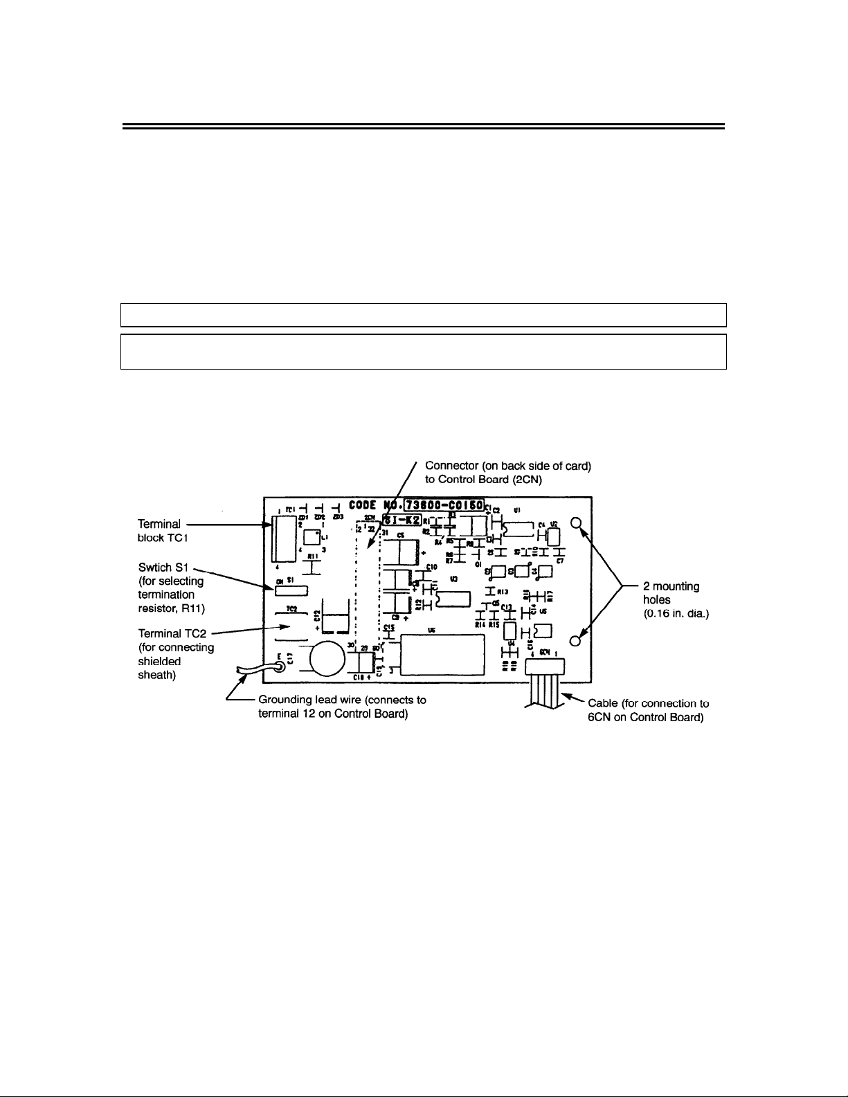
The RS-232D to RS-485 Converter Board
The GPD 515 offers RS-485 serial communications as an option. RS-485 allows a maximum
transmission distance of 4000 feet. RS-485 allows multidrop (multiple devices) communication.
To obtain RS-485 communications an optional converter board must be purchased. This
RS-232D to RS-485 Converter Board is represented by the MagneTek part number CM085.
Read this manual thoroughly before installation, operation, maintenance, and inspection of the
CM085 Option Board.
The CM085 option board employs CMOS technology which may be damaged by static electricity.
Use proper electrostatic discharge (ESD) procedures when handling this board.
The CM085 board is used to convert the drive’s RS-232D standard function to offer RS-485
interface. The following diagram illustrates the CM085 board. (The figure is not actual size.)
CAUTION
Figure 1-1. The CM085 Board
GPD 515 and Serial Communication 1-3
Page 8

Chapter 2
RS-232D Serial Communication
RS-232D Serial Communication
•
•
Figure 2-1. RS-232D Pin-out at 6CN Connector
RS-232D Serial Communication 2-1
Page 9
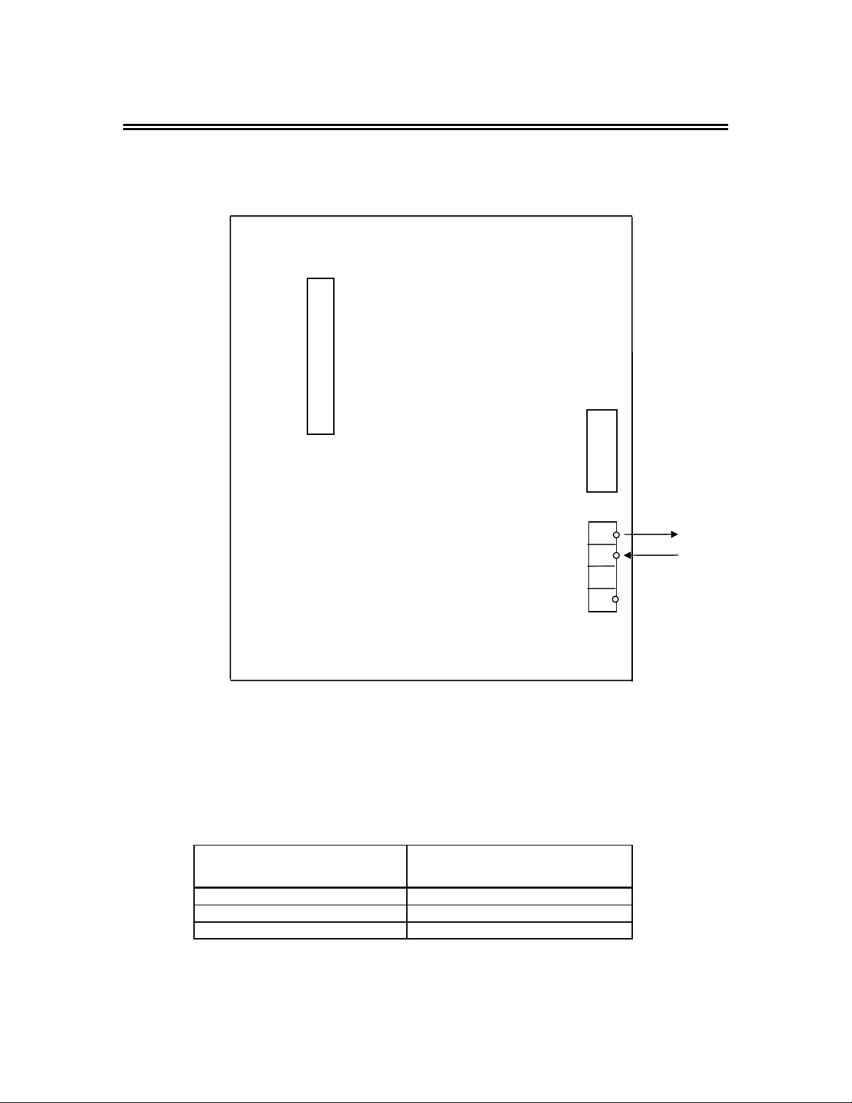
RS-232D Serial Communication
RS-232D Serial Communication is accessed through connector 6CN on the GPD 515ís control
board. Pin 1 on the 6CN connector is for the transmission of data, Pin 2 is for the receipt of data,
and pin 4 is for the ground connection. The RS-232D pin out is shown in the diagram below.
GPD515
2CN
Connector
1CN
Connector
Cable Specifications:
-cable should be a shielded, thin twisted wire 22-28 AWG
-cable pinout is as follows:
Computer - 9 Pin Female
6CN
Connector
Figure 2-1. RS-232D Pin-out at 6CN Connector
GPD 515 Connector for 6CN
D shell
3 - Tx 2 - Rx
2 - Rx 1 - Tx
5 - GND 4 - GND
1
2
3
4
Tx
Rx
GND
-pinout for devices other than a computer (PC), such as a PLC, may vary.
2-2 RS-232D Communication
Page 10

Chapter 3
Installation of the CM085 Board
Installation Procedure
•
• Figure 3-1. Position of the CM085 Board on the
GPD 515 Drive
Installation of the CM086 Board 3-1
Page 11
Installation Procedure
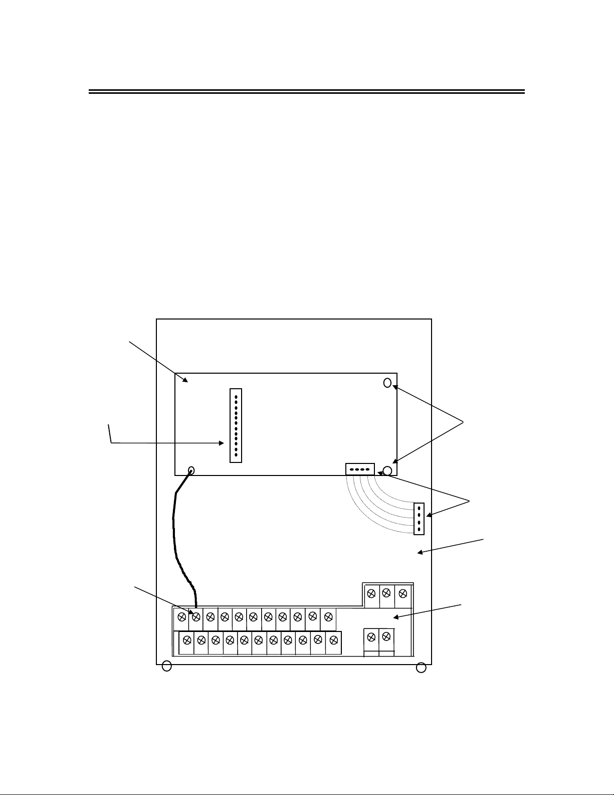
These procedures should be followed when installing the CM085 board into the GPD 515 drive.
1. Turn the main power OFF to the drive. Remove the front cover of the drive to verify that the
CHARGE lamp is off.
2. Position the CM085 board onto the control board of the drive, lining up the 2CN connector on
the CM085 board with the 2CN connector on the control board of the drive.
3. Position the two spacer holes on the right side of the CM085 board with the plastic stand-offs
on the control board. Snap the CM085 board onto the stand-offs tightly.
4. Plug the 6CN cable from the CM085 board into location 6CN on the control board.
5. Connect the green wire (labeled ëEí) from the CM085 board to terminal 12 on the drive.
6. After installing the CM085 board onto the drive, connect with peripheral devices and replace
the cover of the drive.
CM085
Board
2CN
Connector
Ground
Terminal
Spacer Holes
inserted onto
stand-offs
E
6CN
Connection
Drive Control
Board
Main Control
Terminals
Terminal Block
Figure 3-1. Position of the CM085 Board on t he GPD 515 Drive
3-2 Installation of CM086 Board
Page 12

Chapter 4
Wiring of the CM085 Board
Connection of Multiple Drives
•
• Figure 4-1. CM085 Connection Diagram
Wiring Instructions
•
• Figure 4-2. Shielded Wire Termination
• Table 4-1. Functions of Terminal Block TC1
• Table 4-2. Applicable Wire Sizes for Terminal
Block TC1
Terminating Resisto r
•
• Figure 4-3. SW1 Location on the CM085 Board
Wiring of the CM085 Board 4-1
Page 13
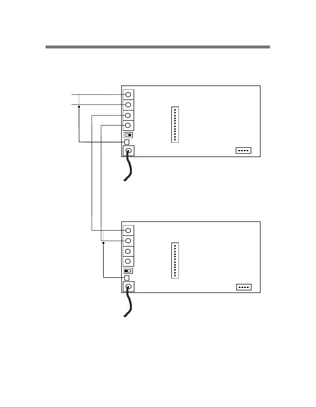
Connection of Multiple Drives
With the RS-485/RS-422 Conversion Board (CM085) multiple drives may be connected together
for a multiple drive communication system. The following diagram illustrates the connection
between multiple CM085 boards.
(+)
RS-485
(-)
Shielded Sheath
Connection
S/R (+)
S/R (-)
S/R (+)
S/R (-)
S/R (+)
S/R (-)
TC1
1
2
3
4
SW1
TC2
Ground
Connection
TC1
1
2
2CN
CM085
BOARD
6CN
2CN
Shielded Sheath
Connection
Figure 4-1. Interconnection Diagram
4-2 Wiring of the CM085 Board
3
4
SW1
TC2
Ground
Connection
CM085
BOARD
6CN
Page 14
Wiring Instructions
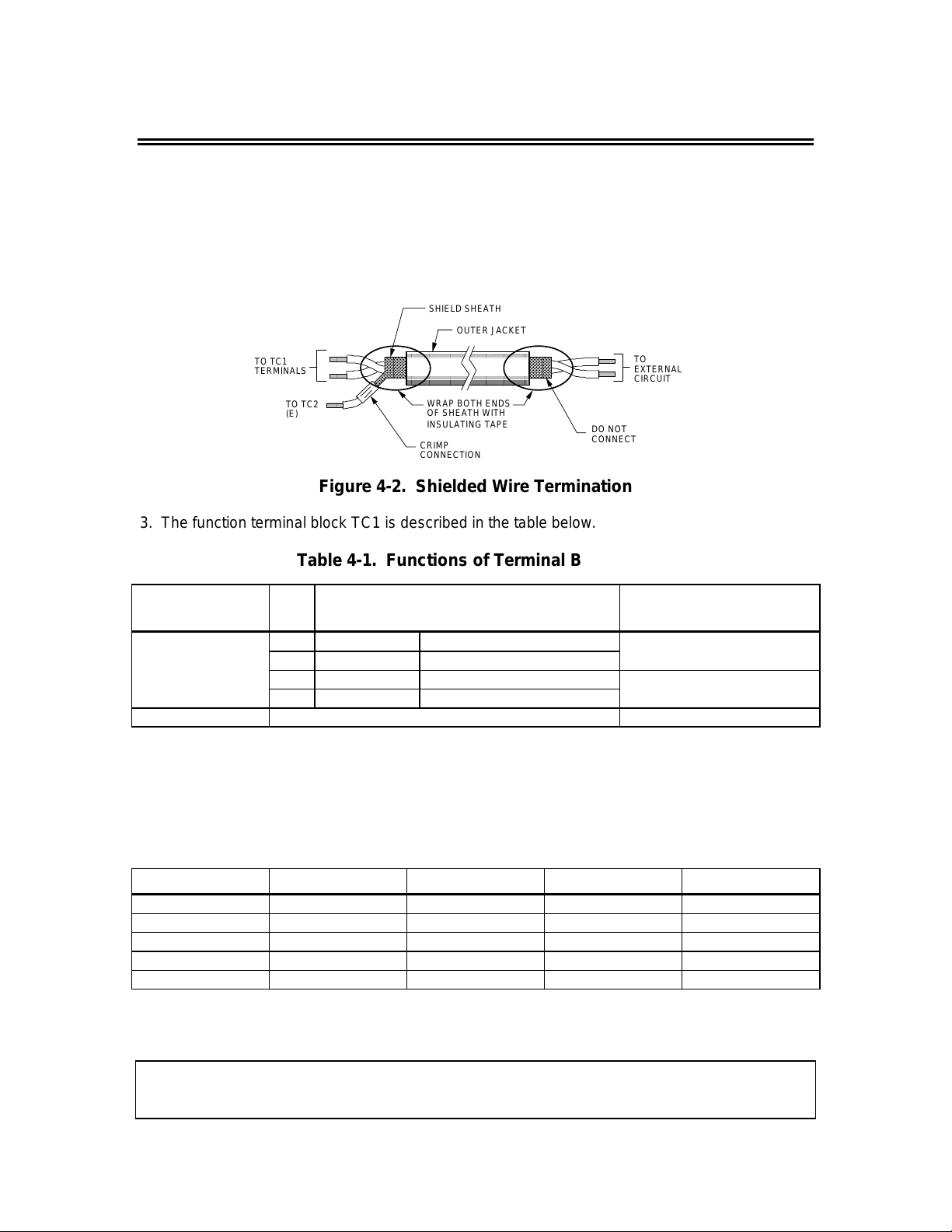
1. Locate terminal block at TC1 on the CM085 board. (See Figure 1-1 in this manual.)
TC1 should have 4 terminal locations (1, 2, 3 and 4) on it.
2. A twisted shielded wire should be used for connection to TC1. The shielded wire should
be separated and connected per the drawing below to eliminate interference due to
noise.
SHIELD SHEATH
OUTER JACKET
DO NOT
CONNECT
TO
EXTERNAL
CIRCUIT
TO TC1
TERMINALS
TO TC2
(E)
WRAP BOTH ENDS
OF SHEATH WITH
INSULATING TAPE
CRIMP
CONNECTION
Figure 4-2. Shielded Wire Termination
3. The function terminal block TC1 is described in the table below.
Table 4-1. Functions of Terminal Block TC1
Terminal Block
Symbol
TC1 2 S/R (-) RS-485 input/output (-) parallel connection
TC2 Shield connection terminal -
4. It is important that an appropriate wire size is selected. When the wire gauge is too thick,
it may apply pressure to the CM085 board and cause failure. When the wire gauge is too
thin, it may lead to imperfect contact or a break in the wire. The table below indicates
the suggested wire size to be used at TC1.
Pin
Functions Remarks
No.
1 S/R (+) RS-485 input/output (+) Use as input at
3 S/R (+) RS-485 input/output (+) Use as output at
4 S/R (-) RS-485 input/output (-) parallel connection
Table 4-2. Applicable Wire Sizes for Terminal Block TC1
[mm2] AWG I [A] VAC [V]
Twisted wire 1.0 16 12 125
Single wire 1.5 16 12 125
UL - 22-16 10 300
CSA - 28-16 10 300
CSA - 28-16 10 150
5. When stripping the wire end to be connected at TC1, approximately 5.5 mm of wire
should be exposed to make a good connection.
Note: Avoid sources of electric interference capable of inducing noise into the cable.
Communication and signal wiring should be kept separate from power wiring. If communication
or signal wiring must cross power wiring, it must cross at a right angle.
Wiring of the CM085 Board 4-3
Page 15
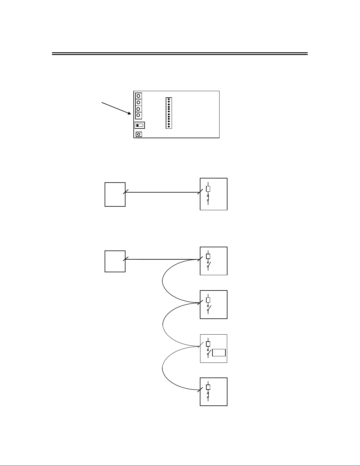
Terminating Resistor
Dip Switch SW1 is located on the lower right hand corner of the CM085 board. (See Figure 4-3
below) When SW1 is on, a termination resistor (100 Ohms) is connected between S/R (+) and
S/R (-).
TC1
1
2
3
4
on
SW1
TC2
Figure 4-3. SW1 Location on the CM085 Board
For one-to-one connections of the CM085 card and a master device set SW1 to ON as shown
below.
RS-485
2CN
CM085
BOARD
ON
Master Device
CM085 Board
If multiple CM085 cards are connected to a master device, set SW1 on the last CM085 board to
ON as shown below.
RS-485
OFF
Master Device
CM085 Board
OFF
CM085 Board
OFF
CM085 Board
4-4 Wiring of the CM085 Board
ON
CM085 Board
Page 16

Chapter 5
Setting GPD 515 Parameters for
Communication
Run/Stop and Frequency Selection
•
Communication Set up Parameters
•
ìENTERî C ommand
•
Setting GPD 515 Parameters for Communication 5-1
Page 17

Run/Stop and Frequency Selection
The run/stop commands and frequency reference command can originate from serial
communication, the Digital Operator, the external terminals, or an option board. The origin of the
run/stop command does not have to be the same as the origin for the frequency reference
command. Parameter b1-01 (Reference Selection) allows you to set up the origin of the
frequency reference, and parameter b1-02 (Operatoin Mode Selection) sets the origin of the
run/stop commands. Parameter b1-01 is Modbus register number 180h, and b1-02 is Modbus
register 181h. The charts shown below illustrate the possible frequency reference and run/stop
selections.
Parameter b1-01 (180h)
Setting
0 Digital Operator
1 External Terminals
2 Serial Communication
3 Option board
The default setting of parameter b1-01 is ë1í.
Parameter b1-02 (181h)
Setting
0 Digital Operator
1 External Terminals
2 Serial Communication
3 Option board
The default setting of parameter b1-02 is ë1í.
Frequency Reference Selection
Operation Method Selection
(Run/Stop)
5-2 Setting GPD 515 Parameters for Communication
Page 18

Serial Communication Set up Parameters
The GPD 515 has parameters used for the set up of serial communication. These
communication set up parameters are H5-01 through H5-05 and o2-09.
Parameter H5-01 - Serial Communication Station Address
Parameter H5-01 (or Modbus Register 41Ch) is used to set the Modbus slave address of the GPD
515 drive. The slave address can be any number from 1 to 1F in hexadecimal (or 1 to 31
decimal). Two nodes may not have the same address. The default setting for parameter H5-01
is ë1Fíh.
Parameter H5-02 - Serial Communication Baud Rate Selection
Parameter H5-02 (or Modbus Register 41Dh) is used to select the baud rate. The table below
indicates the baud rates that may be selected.
Setting Value (in hex) Baud Rate Selection
0 1200 bps
1 2400 bps
2 4800 bps
3 9600 bps
The default setting of parameter H5-02 is ë3í.
Parameter H5-03 - Serial Communication Parity Selection
Parameter H5-03 (or Modbus Register 41Eh) is used to select the parity . The table below
indicates the parity that may be selected.
Setting Value (in hex) Parity Selection
0 No parity
1 Even parity
2 Odd parity
The default setting of parameter H5-03 is ë0í.
Communication Error (CE)
A communication error can occur only after communication has been established between the
master and the drive. The drive waits for the master to initiate communication.
The message data is always checked for CRC, parity, overrun, framing, and overflow. If the data
has discrepancies in any of these areas a communication error will occur. If the drive does not
receive a message (addressed to its appropriate slave address set up in H5-01) within a period of
2 seconds, a time-out occurs. A time-out can also cause a communication error if it is enabled
(see parameter H5-05).
Parameters H5-04 and H5-05 are the set up parameters that determine how the drive will respond
to a communication error.
Setting GPD 515 Parameters for Communication 5-3
Page 19

Parameter H5-04 - Stopping Method after Serial Communication Error
Parameter H5-04 (or Modbus Register 41Fh) is used to determine the method of stopping the
motor if there is a communication error. The table below indicates the stopping methods that can
be used when a communication error occurs.
Setting Value (in hex) Stopping Method
0 Decelerate to stop
1 Coast to stop
2 Fast Stop
3 Alarm Only / Continue Operation
The default setting of parameter H5-04 is ë3í.
Parameter H5-05 - Serial Fault Detection Selection
Parameter H5-05 (or Modbus Register 420h) is used to enable or disable the Time-out detection.
The table below indicates how to enable or disable the communication error.
Setting Value (in hex) Time-out Detection Selection
0 disabled
1 enabled
The default setting of parameter H5-05 is ‘1’.
Parameter o2-09 - Initial Mode Select
Parameter o2-09 (or Modbus Register 50Dh) determines the Modbus Register Address of the
operational signals register and frequency reference register. Set this parameter to ë1í so that the
Modbus Register Addresses of the Operation Signal register is 001h and the Frequency
Reference register is 002h. The Modbus Register Address for Operation Signals is 00h and the
Frequency Reference register is 01h for flach software versions previous to ‘1024’ and CPU
version ‘20’.
The default setting for parameter o2-09 is ‘0’.
Note: Power must be cycled to the drive,
to make the serial communication set up parameters effective.
5-4 Setting GPD 515 Parameters for Communication
Page 20

ìENTERî Command
The GPD 515 has two types of memory: ëVolatileí and ëNon-Volatileí. Data held in the Volatile
memory will be lost when power is removed from the drive. Data held in Non-Volatile memory will
be retained when power is removed from the drive. Different types of registers are stored in
different areas of memory.
Command Data:
The command registers (000h to 00Fh) are stored in Volatile memory. When writing to a
command register the new data becomes active immediately. In the case of a power loss all data
stored in these registers will not be retained.
Monitor Data:
The monitor registers (010h to 01Fh) are stored in Volatile memory. These registers can not be
written to (read only registers). Any data read from the monitor registers will not be retained
during a power loss situation.
Parameter Data:
The parameter registers (100h to 50Dh) are stored in Non-Volatile memory. When writing new
data to parameter registers, an ëENTERí command must be given for the new data to become
active.
There are two different types of ëENTER’ commands, ‘ACCEPT’ and ‘ENTER’. For an ‘ACCEPT’,
write the value ‘0’ to Modbus register FFDDh. This causes data to become “active”. If a power
loss occurs, the data will not be retained. For an ‘ENTER’, write the value ‘0’ to Modbus register
FFFDh. This causes data to become “active” and saves the date to Non-Volatile memory. If a
power loss occurs, the data will be retained.
Some Parameter Data registers may be written to while the drive is running. These parameters
are called run operative parameters. For a list of these paremeters, refer to Appendix A, Table
A1-11 of the GPD 515 technical manual (TM 4515).
All other Parameter Data registers may only be written to when the drive is stopped. These are
called non-run operative parameters.
If new data is written to any parameter serially, and is not followed by an ‘ENTER’ command, a
“Busy Write Protected” message will flash on the Digital Operator display if an attempt is then
made to change a parameter using the Digital Operator.
The same message will be displayed if an attempt is made to change a parameter via the Digital
Operator while the contents of the ‘ENTER’ command register is any value other than ‘0’.
NOTE
Use the ‘ENTER’ (FFFDh) command only when necessary!
The life of the EEPROM (Non-Volatile memory) on the GPD 515 will support a finite number of
operations. This means that the ‘ENTER’ command, value ‘0’ written to
register FFFDh, can only be used a maximum of a 100,000 times to store data in the EEPROM.
After the specified number of operations, the EEPROM may fault
control board to be replaced.
(ERR)
requiring the GPD 515
Setting GPD 515 Parameters for Communication 5-5
Page 21

Chapter 6
The Message Format
Message Functions
•
Read Multiple Registers
•
Loop Back Test
•
Write Multiple Registers
•
No Response Message
•
CRC-16
•
The Message Format 6-1
Page 22

Message Functions
In communicating to the GPD 515 drive via Modbus RTU, there are three message functions
available. The master specifies the function to be executed by the slave according to the function
code. The following table shows the types of function codes available, and the length (quantity)
and contents of the message according to the function.
Function
Code (hex)
3 Read Multiple Registers 8 8 7 37
8 Loop-back test 8888
10 Write Multiple Registers 11 41 8 8
The message format varies depending upon the function of the message. For each function,
there is a command message from the master and a response message initiated from the slave.
The following sections review the format of the command message and the response message
for each function.
Function
Command
Message
min.
(bytes)
max.
(bytes)
Response
Message (Normal)
min.
(bytes)
max.
(bytes)
6-2 The Message Format
Page 23

Read Multiple Registers - 03h
N
The multiple register read function (03h) allows the master to request information from the slave.
The command message of a multiple register read is structured as shown below.
Command Message
SLAVE ADDRESS
FUNCTION CODE
STARTING
REGISTER
O.
UPPER
LOWER
UPPER
03h
00h
20h
00h
QTY.
LOWER
LOWER
04h
45h
CRC-16
UPPER
F0h
Each GPD 515ís slave address is set in advance by the drive parameter H5-01. Valid slave
addresses must be in the range of 1 to 31 decimal (1 to 1F hex). No two slaves may have the
same address. The master addresses the slave by placing the slave address in the address field
of the message. In the command message above, the slave is addressed at 2.
The function code of this message is 03h (read multiple registers).
The starting number is the first register to be read. In the command message above the starting
register is 20h, indicating that the first register is the Frequency Reference. A listing of the GPD
515ís registers is shown in Chapter 7, Registers.
The quantity indicates how many consecutive registers are to be read. The quantity may range
from 1 to 16 registers. If the quantity is greater than 16, an error code of ë3í is returned in the
fault response message. In this command message there is four consecutive registers to be
read: 20h-Frequency Reference, 21h-Output Frequency, 22h-Output Current, and 23h-Control
Method.
A CRC-16 value is generated from a calculation using the values of the address, function code,
and data sections of the message. The procedure for calculating a CRC-16 is described at the
end of this chapter. When the slave receives the command message it calculates a CRC-16
value and compares it to the one in CRC-16 field of the command message. If these two CRC-16
values are the same the slave has received the proper command message. If the two CRC-16
values are not the same the slave will not respond.
If the command message has a valid slave address, function code, starting register, and quantity
value, the slave will respond with a normal response message. If the command message has an
invalid slave address, function code, starting register, and/or quantity the slave will respond with a
fault response message.
The Message Format 6-3
Page 24

6-4 The Message Format
Page 25

Normal Response Message
SLAVE ADDRESS
FUNCTION CODE
NO. OF DATA BYTES
STARTING
REGISTER
CONTENTS
UPPER
LOWER
03h
08h
17h
70h
The starting register, 20h
(Frequency Reference),
has a value of 1770h or
6000 dec. (60.00 Hz)
The next register, 21h
(Output Freque ncy), has
a value of 1770h or 6000
dec. (60.00 Hz).
The next register, 22h
(Output Current), has a
value of 109h or 265 dec.
NEXT
REGISTER
CONTENTS
NEXT
REGISTER
CONTENTS
UPPER
LOWER
UPPER
LOWER
17h
70h
01h
09h
(drive rating / 8192).
NEXT
REGISTER
CONTENTS
UPPER
LOWER
00h
00h
The next register, 23h
(Control Method), has a
value of 00h or 0 dec.
CRC-16
LOWER
UPPER
38h
AC
h
(V/f Control).
The normal response message contains the same slave address and function code as the
command message, indicating to the master which slave is responding and to what type of
function it is responding.
The number of data bytes is the number of data bytes returned in the response message. The
number of data bytes is actually the quantity (in the command message) times 2, since there are
two bytes of data in each register.
The data section of the response message contains 8 upper and 8 lower bits of data for each
register that has been read from the drive.
A CRC-16 value is generated from a calculation using the values of the address, function code,
number of data bytes, and register data sections of the message. The procedure for calculating a
CRC-16 value is described at the end of this chapter. How the response message is handled by
the master depends on what master is used. When the master receives the response message it
should calculate a CRC-16 value and compare it to the one in the CRC-16 field of the response
message. If these two CRC-16 values are the same the master has received the proper
response message.
The Message Format 6-5
Page 26

Fault Response Message
SLAVE ADDRESS
80h + FUNC. CODE
ERROR CODE
LOWER
CRC-16
UPPER
83h
02h
30h
F1h
The fault response message contains the same slave address as the command message,
indicating to the master which slave is responding.
The function code of a fault response message is actually a value of 80h plus the original function
code of 03h. This indicates to the master that the message is a fault response message, instead
of a normal response message.
The error code indicates where the error occurred in the command message. The value of 2h in
the error code field of this fault response message, indicates that the command message
requested data be read from an invalid register. A complete listing of the error codes is shown in
Chapter 8, Troubleshooting and Error Codes.
A CRC-16 value is generated from a calculation using the values of the address, function code,
and error code sections of the message. The procedure for calculating a CRC-16 value is
described at the end of this chapter. How the response message is handled by the master
depends on what master is used. When the master receives the fault response message it
should calculate a CRC-16 value and compare it to the one in the CRC-16 field of the fault
response message. If these two CRC-16 values are the same the master has received the
proper fault response message.
6-6 The Message Format
Page 27

Loop-back Test - 08h
The loop-back test function (08h) is used for checking signal transmission between master and
slaves. The command message format is shown below.
Command Message
SLAVE ADDRESS
FUNCTION CODE
TEST
UPPER
08h
00h
CODE
LOWER
UPPER
00h
A5h
DATA
LOWER
LOWER
37h
DAh
CRC-16
UPPER
8Dh
Each GPD 515ís slave address is set in advance by the drive parameter H5-01. Valid slave
addresses must be in the range of 1 to 31 decimal (1 to 1F hex). No two slaves may have the
same address. The master addresses the slave by placing the slave address in the address field
of the message. In the command message above, the slave is addressed at 1.
The function code of this message is 08h (loop-back test).
The test code must be set to ë0000í. This function specifies that the data passed in the
command message is to be returned (looped back) in the response message.
The data section contains arbitrary data values. These data values are used to verify that the
slave receives the correct data.
A CRC-16 value is generated from a calculation using the values of the address, function code,
test code, and data sections of the message. The procedure for calculating a CRC-16 is
described at the end of this chapter. When the slave receives the command message it
calculates a CRC-16 value and compares it to the one in CRC-16 field of the command message.
If these two CRC-16 values are the same the slave has received the proper command message.
If these two CRC-16 values are not the same the slave does not respond.
If the command message has a valid slave address, function code, test code, and data value, the
slave will respond with a normal response message. If the command message has an invalid
slave address, function code, test code, and/or data value the slave will respond with a fault
response message.
The Message Format 6-7
Page 28

Normal Response Message
SLAVE ADDRESS
FUNCTION CODE
TEST
UPPER
08h
00h
CODE
LOWER
UPPER
00h
A5h
DATA
LOWER
LOWER
37h
DAh
CRC-16
UPPER
8Dh
A normal response message for the loop-back test should be identical to the command message.
Fault Response Message
SLAVE ADDRESS
80h + FUNC. CODE
ERROR CODE
88h
01h
CRC-16
LOWER
UPPER
87h
C0h
The fault response message contains the same slave address as the command message,
indicating to the master which slave is responding.
The function code of a fault response message is actually a value of 80h plus the original function
code of 08h. This indicates to the master that the message is a fault response message, instead
of a normal response message.
The error code indicates where the error occurred in the command message. A complete listing of
the error codes is shown in Chapter 8, Troubleshooting and Error Codes.
A CRC-16 value is generated from a calculation using the values of the address, function code,
and data sections of the message. The procedure for calculating a CRC-16 value is described at
the end of this chapter. How the response message is handled by the master depends on what
master is used. When the master receives the fault response message it should calculate a
CRC-16 value and compare it to the one in the CRC-16 field of the fault response message. If
these two CRC-16 values are the same the master has received the proper fault response
message.
6-8 The Message Format
Page 29

Write Multiple Registers - 10h
N
The multiple register write function (10h) allows the master to write data to the driveís registers.
The multiple register write message format is shown below.
Command Message
SLAVE ADDRESS
FUNCTION CODE
STARTING
REGISTER
O.
UPPER
LOWER
UPPER
QTY.
LOWER
NO. OF DATA BYTES
UPPER
DATA TO
FIRST
REGISTER
DATA TO
NEXT
REGISTER
LOWER
UPPER
LOWER
LOWER
CRC-16
10h
00h
01h
00h
02h
04h
00h
01h
17h
70h
6Dh
The first register, 01h
(Operation Command) has
a value of 01h or 1 dec.
(forward run command)
The next register, 02h
(Frequency Reference) has
a value of 1770h or 6000
dec. (60.00 Hz)
UPPER
B7h
Each GPD 515ís slave address is set in advance by the drive parameter H5-01. Valid slave
addresses must be in the range of 1 to 31 decimal (1 to 1F hex). No two slaves may have the
same address. The master addresses the slave by placing the slave address in the address field
of the message. In the command message above, the slave is addressed at 1.
By setting the slave address to zero (0) in the address section of the message, the master can
send operation signals (register 1h) and frequency reference (register 2h) to all slaves on the
network. The master can send a single transmission to all the slaves simultaneously. This is
called simultaneous broadcasting. In a simultaneous broadcast message all of the slaves on the
network act upon one message. Simultaneous Broadcast registers are shown in Chapter 7,
Registers (page 7-2).
The function code of this message is 10h (write multiple registers).
The starting register number is the first register to be written to. In the command message above
the starting number is 01h, indicating that the first register is the frequency reference. A listing of
the GPD 515ís registers is shown in Chapter 7, Registers.
The Message Format 6-9
Page 30

6-10 The Message Format
Page 31

The quantity indicates how many consecutive registers are to be written to. The quantity may
range from 1 to 16 registers. If the quantity is greater than 16, an error code of ë3í is returned in
the fault response message. In this command message there is two consecutive registers to be
written to: 01h-Operation Command and 02h- Frequency Reference.
The number of data bytes is the number of bytes of data to be written to the drive. The number of
data bytes is actually the quantity times 2, since there are two bytes of data in each register.
The data section of the response message contains 8 upper and 8 lower bits of data for each
register that is being written to.
A CRC-16 value is generated from a calculation using the values of the address, function code,
starting register number, quantity, number of data bytes, and data sections of the message. The
procedure for calculating a CRC-16 is described at the end of this chapter. When the slave
receives the command message it calculates a CRC-16 value and compares it to the one in CRC16 field of the command message. If these two CRC-16 values are the same the slave has
received the proper command message. If these two CRC-16 values are not the same the slave
does not respond.
If the command message has a valid slave address, function code, starting register number,
quantity, number of data bytes, and data values, the slave will respond with a normal response
message. If the command message has an invalid slave address, function code, starting register
number, quantity, number of data bytes, and/or data values the slave will respond with a fault
response message.
Normal Response Message
SLAVE ADDRESS
FUNCTION CODE
STARTING
REGISTER
NUMBER
UPPER
LOWER
UPPER
10h
00h
01h
00h
QTY.
LOWER
LOWER
02h
10h
CRC-16
UPPER
08h
The normal response message contains the same slave address and function code as the
command message, indicating to the master which slave is responding and to what type of
function it is responding.
The starting number is the first register that was written to. In the response message above the
starting number is 01h, indicating that the first register is the operation command.
The quantity indicates how many consecutive registers were written to.
The Message Format 6-11
Page 32

A CRC-16 value is generated from a calculation using the values of the address, function code,
starting register number, and quantity value of the message. The procedure for calculating a
CRC-16 value is described at the end of this chapter. How the response message is handled by
the master depends on what master is used. When the master receives the response message it
should calculate a CRC-16 value and compare it to the one in the CRC-16 field of the response
message. If these two CRC-16 values are the same the master has received the proper
response message.
Fault Response Message
SLAVE ADDRESS
80h + FUNC. CODE
ERROR CODE
LOWER
90h
02h
CDh
CRC-16
UPPER
C1h
The fault response message contains the same slave address as the command message,
indicating to the master which slave is responding.
The function code of a fault response message is actually a value of 80h plus the original function
code of 10h. This indicates to the master that the message is a fault response message, instead
of a normal response message.
The error code indicates where the error occurred in the command message. The value of 2h in
the error code field of this fault response message, indicates that the command message
requested data to be written to an invalid register. A complete listing of the error codes is shown
in Chapter 8, Troubleshooting and Error Codes.
A CRC-16 value is generated from a calculation using the values of the address, function code,
and error code sections of the message. The procedure for calculating a CRC-16 value is
described at the end of this chapter. How the response message is handled by the master
depends on what master is used. When the master receives the fault response message it
should calculate a CRC-16 value and compare it to the one in the CRC-16 field of the response
message. If these two CRC-16 values are the same the master has received the proper
response message.
6-12 The Message Format
Page 33

No Response Message
The slave disregards the command message and does not return the respond message in the
following cases:
1.
In simultaneous broadcasting of data (slave address field is 0), all slaves execute but
do not respond.
2.
When a communication error (overrun, framing, parity, or CRC-16) is detected in the
command message.
3.
When the slave address in the command message does not coincide with the address
set in the slave.
4.
When the command message data length is not proper.
CRC-16
At the end of the message, the data for CRC error checking is sent in order to detect errors in
signal transmission. In Modbus RTU, the error check is conducted in the form of a CRC-16
(Cyclical Redundancy Check). The CRC field checks the contents of the entire message. It is
applied regardless of any parity check method used for the individual characters of the message.
The CRC field is two bytes, containing 16-bit binary value. The CRC value is calculated by the
transmitting device, which appends the CRC to the message. The receiving device recalculates a
CRC during receipt of the message, and compares the calculated value to the actual value it
received in the CRC field. If the two values are not equal, an error results.
The CRC is started by first preloading a 16-bit register to all 1ís. Then a process begins of
applying successive 8-bit bytes of the message to the current contents of the register. Only the
eight bits of data in each character are used for generating the CRC. Start and stop bits, and the
parity bit (if one is used) do not apply to the CRC.
During generation of the CRC, each 8-bit character is exclusive ëORíed with the register contents.
Then the result is shifted in the direction of the least significant bit (LSB), with a zero filled into the
most significant bit (MSB) position. The LSB is extracted and examined. If the LSB is a 1, the
register is then exclusive ëORíed with a preset, fixed value (A001h). If the LSB is a 0, no
exclusive OR takes place.
This process is repeated until eight shifts have been performed. After the last (eighth) shift, the
next 8-bit byte is exclusive ëORíed with the registerís current value, and the process repeats for
eight more shifts as described above. The final contents of the register, after all the bytes of the
message have been applied, is the CRC value.
For applications using a host computer, a detailed example of a CRC generation using Quick
Basic is shown on the following page.
The Message Format 6-13
Page 34

Typical CRC-16 Calculation Program in Quick Basic:
crcsum# = &HFFFF&
crcshift# = &H0&
crcconst# = &HA001&
CLS
PRINT "***************************************************"
PRINT
PRINT " CRC-16 calculator"
PRINT
PRINT "***************************************************"
PRINT "If entering data in hex, preceed the data with '&H'"
PRINT " Example: 32decimal = 20hex = &H20"
PRINT "***************************************************"
PRINT
INPUT "Enter the number of bytes in the message: ", maxbyte
FOR bytenum = 1 TO maxbyte STEP 1
PRINT "Enter byte "; bytenum; ":":
INPUT byte&
byte& = byte& AND &HFF&
crcsum# = (crcsum# XOR byte&) AND &HFFFF&
FOR shift = 1 TO 8 STEP 1
crcshift# = (INT(crcsum# / 2)) AND &H7FFF&
IF crcsum# AND &H1& THEN
crcsum# = crcshift# XOR crcconst#
ELSE
crcsum# = crcshift#
END IF
NEXT shift
NEXT bytenum
lower& = crcsum# AND &HFF&
upper& = (INT(crcsum# / 256)) AND &HFF&
PRINT "Lower byte (1st) = ", HEX$(lower&)
PRINT "Upper byte (2nd) = ", HEX$(upper&)
6-14 The Message Format
Page 35

CRC-16 Calculation Example:
A two byte message for a read-out of a
specified coil status is as follows.
0000 0010
0000 0111
Slave Address = 2
Function Code = 7
The actual CRC calculation would look like
this:
CRCTMP FLAG
1111 1111 1111 1111 Initial Value
0000 0010 Slave Address
1111 1111 1111 1101 Result of EX
OR
0111 1111 1111 1110 1 Shift #1
1010 0000 0000 0001 CRC-16
constant A001h
1101 1111 1111 1111 Result of EX
OR
0110 1111 1111 1111 1 Shift #2
1010 0000 0000 0001 CRC-16
constant A001h
1100 1111 1111 1110 Result of EX
OR
0110 0111 1111 1111 0 Shift #3
0011 0011 1111 1111 1 Shift #4
1010 0000 0000 0001 CRC-16
constant A001h
1001 0011 1111 1110 Result of EX
OR
0100 1001 1111 1111 0 Shift #5
0010 0100 1111 1111 1 Shift #6
1010 0000 0000 0001 CRC-16
constant A001h
1000 0100 1111 1110 Result of EX
OR
0100 0100 0111 1111 0 Shift #7
0010 0001 0011 1111 1 Shift #8
1010 0000 0000 0001 CRC-16 constant A001h
1000 0001 0011 1110 Result of EX
OR
0000 0111 Function Code
1000 0001 0011 1001 Result of EX
OR
0100 0000 1001 1100 1 Shift #1
1010 0000 0000 0001 CRC-16
constant A001h
1110 0000 1001 1101 Result of EX
OR
0111 0000 0100 1110 1 Shift #2
1010 0000 0000 0001 CRC-16
constant A001h
1101 0000 0100 1111 Result of EX
OR
0110 1000 0010 0111 1 Shift #3
1010 0000 0000 0001 CRC-16
constant A001h
1100 1000 0010 0110 Result of EX
OR
0110 0100 0001 0011 0 Shift #4
0011 0010 0000 1001 1 Shift #5
1010 0000 0000 0001 CRC-16
constant A001h
1001 0010 0000 1000 Result of EX
OR
0100 1001 0000 0100 0 Shift#6
0010 0100 1000 0010 0 Shift #7
0001 0010|0100 0001 0 Shift #8
1 2 4 1
CRC-16
(Upper 8)
CRC-16
(Lower 8)
The Message Format 6-15
Page 36

After calculating the CRC-16 upper and
lower values they are inserted into the
message format as shown below.
0000 0010
0000 0111
0100 0001
0001 0010
Slave Address = 2
Function Code = 7
CRC-16 Lower = 41h
CRC-16 Upper = 12h
6-16 The Message Format
Page 37

Chapter 7
Registers
Simultaneous Broadcast Registers
•
Command Registers
•
Monitor Registers
•
Drive Parameter Re gisters
•
Special Registers
•
Registers 7-1
Page 38

Simultaneous Broadcast Registers (Write only)
p
REGISTER FUNCTION BIT DATA DESCRIPTION
(in hex) NO. SET
001* Operational Signals 0 0 Sto
1 Run
1 0 Forward Run
1 Reverse Run
2 not used
3 not used
4 1 External Fault
5 1 Fault Reset
6 not used
7 not used
002* Frequency Reference
Notes:
1. Scaling depends on the setting of o1-03.
* Set parameter o2-09 to ‘1’ so that the Modbus Register Address of the Operation Signals register is 01h and the Frequency Reference register is 02h. The
Modbus Register Address for Operation Signals register is 00h and the Frequency Reference is 01h for flash software versions previous to ‘1024’
and CPU version ‘20’.
Frequency Reference (6000 = 100%)
(1)
7-2 Registers
Page 39

Command Registers (Read / Write)
g
(5)
g
(6)
(3)
(4)
)
REGISTER FUNCTION BIT DESCRIPTION
(in hex) NO.
001* Operational Signals 0 Forward operation
1 Reverse Operation
2 Closed External Terminal 3
3 Closed External Terminal 4
4 Closed External Terminal 5
5 Closed External Terminal 6
6 Closed External Terminal 7
7 Closed External Terminal 8
002* Frequency Reference / Output Frequency
003
004
005 Not Supported will return zeros
006 Not Supported will return zeros
007 Analog Output 1 Settin
008 Analog Ouptut 2 Settin
009 Contact Output Setting 0
1
2
3 not used
4 not used
5 not used
6 Fault Contact code
7 Fault Contact state (effective only when bit 6 = ‘1’
00A-00Fh Reserved return all zeros
–10V / –660 to +10V / +660 analog output on terminals 21 & 22
–10V / –660 to +10V / +660 analog output on terminals 22 & 23
Multi-function Contact Output (terminals 9 & 10): “closed”
Multi-function Contact Output (terminals 25 & 27): “closed”
Multi-function Contact Output (terminals 26 & 27): “closed”
1 Hz / 100
(1)
(2)
Notes:
1. Desired frequency of 35.75 Hz requires a value of 3575 in register data code 002h. Scaling depends on the setting of o1-03.
2. Effective when H2-01 = 0Fh.
3. Effective when H2-02 = 0Fh.
4. Effective when H2-03 = 0Fh.
5. Effective when H4-01 = 1Fh.
6. Effective when H4-04 = 1Fh.
* Set parameter o2-09 to ‘1’ so that the Modbus Register Address of the Operation Signals register is 01h and the Frequency Reference register is 02h. The
Modbus Register Address for Operation Signals register is 00h and the Frequency Reference is 01h for flash software versions previous to ‘1024’
and CPU version ‘20’.
7-3 Registers
Page 40

Monitor Registers (Read only)
y
(
)
)
)
)
)
)
ge (oV)
)
)
)
)
)
)
)
)
REGISTER FUNCTION BIT DESCRIPTION
(in hex) NO.
010h Status Signal 0 Run Command
1 At zero speed
2 Reverse Operation
3 Reset Signal Input
4 Speed Agreed
5 Drive Read
6 Minor Fault
7 Major Fault
8-15 will return zeros
011h Drive Fault Contents 0 oPE Error
1 not used
2 Program Mode
3 1CN Status:
4
5-15 not used
012h oPE No. oPE Error Code (oPE01=1, oPE02=2, oPE03=3, oPE06=6, oPE10=10, oPE11=11)
013h not used will return zeros
014h Fault Content 1 0 Fuse Blown (FU)
1 DC Bus Undervoltage (UV1
2 Control Power Supply Undervoltage (UV2
3 Main Circuit Answerback (UV3
4 Short Circuit (SC
5 Ground Fault (GF
6 Overcurrent (oC
7Overvolta
8 Heatsink Overtemperature (oH
9 Drive Overheat (oH1
10 Motor Overload (oL1
11 Drive Overload (oL2
12 Overtorque 1 (oL3
13 Overtorque 2 (oL4
14 Dynamic Braking Transistor (RR
15 Dynamic Braking Resistor (RH
01
=JVOP132 / 00=JVOP130
std. operator) / 11=Personal Computer / 10=JVOP100
7-4 Registers
Page 41

Monitor Registers (continued)
)
)
)
)
)
p
)
p
)
p
)
)
)
)
)
)
)
)
REGISTER FUNCTION BIT DESCRIPTION
(in hex) NO.
015h Fault Content 2 0 External Fault 3 (EF3)
1 External Fault 4 (EF4
2 External Fault 5 (EF5
3 External Fault 6 (EF6
4 External Fault 7 (EF7
5 External Fault 8 (EF8
6 not used
7Overs
8 S
9PG O
10 Input Phase Loss (PF
11 Output Phase Loss (LF
12 DCCT Fault (CF
13 Operator Disconnected (OPR
14 EEPROM Write-in Fault (ERR
15 not used
016h Fault Content 3 0 Modbus Communication Error (CE)
1 not used
2 not used
3 not used
4 Control Fault (CF
5 Zero Servo Fault (SVE
6-15 not used
017h CPF Content 1 0 not used
1 not used
2 CPF02 Fault
3 CPF03 Fault
4 CPF04 Fault
5 CPF05 Fault
6 CPF06 Fault
7-15 not used
eed Deviation (DEV
eed (oS
en (PGo
7-5 Registers
Page 42

Monitor Registers (continued)
)
)
)
)
)
)
)
)
)
)
)
)
)
)
)
)
)
)
)
)
REGISTER FUNCTION BIT DESCRIPTION
(in hex) NO.
018h CPF Content 2 0 CPF20 Fault
1 CPF21 Fault
2 CPF22 Fault
3 CPF23 Fault
4-15 not used
019h Minor Fault Content 1 0 Undervoltage Detection (UV)
1 Overvoltage Detection (oV
2 Heatsink Overtemperature (oH
3 Drive Overheat Alarm (oH1
4 Overtorque 1 Detection (oL3
5 Overtorque 2 Detection (oL4
6 2-wire Sequence Input Fault (EF
7 During External Baseblock (BB
8 External Fault 3 (EF3
9 External Fault 4 (EF4
10 External Fault 5 (EF5
11 External Fault 6 (EF6
12 External Fault 7 (EF7
13 External Fault 8 (EF8
14 Cooling Fan Fault (FAN
15 Overspeed (oS
01Ah Minor Fault Content 2 0 Speed Deviation (DEV)
1 PG Open (PGo
2 Operator Disconnected (OPR
3 Modbus Communication Error (CE
4 not used
5 not used
6 Motor Overload (oL1
7 Drive Overload (oL2
8-15 not used
7-6 Registers
Page 43

Drive Parameter Registers (U1-XX / Monitor Only)
REGISTER PARAMETER PARAMETER PARAMETER BIT LIMITS / DESCRIPTION
(in hex) FUNCTION SETTING NO.
020h U1-01 Frequency Reference
021h U1-02 Output Frequency
022h U1-03 Output Current Drive rating / 8192
023h U1-04 Control Method
024h U1-05 Motor Speed Motor Speed (in 0.1 Hz)
025h U1-06 Output Voltage Output Voltage (in 0.1 V)
026h U1-07 DC Bus Voltage DC Bus Voltage (in 1 V)
027h U1-08 Output Power Output Power (in 0.1 kW)
028h U1-09 Torque Reference Torque Reference (in 0.1%)
029h U1-10 Input Terminal Status 0 Input Terminal 1 closed
02Ah U1-11 Output Terminal Status 0 Control Circuit terminals 9 & 10: ìClosedî
Frequency Reference of drive (0.1 Hz)
Output Frequency of drive (0.1 Hz)
0
1 V/f with PG Feedback
2 Open Loop Vector
3 Flux Vector
1 Input Terminal 2 closed
2 Input Terminal 3 closed
3 Input Terminal 4 closed
4 Input Terminal 5 closed
5 Input Terminal 6 closed
6 Input Terminal 7 closed
7 Input Terminal 8 closed
1 Control Circuit terminals 25 & 27: ìClosedî
2 Control Circuit terminals 26 & 27: ìClosedî
3-6 not used
7 Control Circuit terminals 18 & 20: ìClosedî
V/f Control
(1)
(1)
Notes (for this page only):
1. Scaling depends on setting of o1-03.
7-7 Registers
Page 44

Drive Parameter Registers (U1-XX / Monitor Only) (continued)
REGISTER PARAMETER PARAMETER PARAMETER BIT LIMITS / DESCRIPTION
(in hex) FUNCTION SETTING NO.
02Bh U1-12 Operation Status 0 Run
02Ch U1-13 Elapsed Time hours
02Dh U1-14 Software No. (CPU ID No.) software version number
02Eh U1-15 Control Circuit Term 13 Input Voltage
02Fh U1-16 Control Circuit Term 14 Input Voltage
030h U1-17 Control Circuit Term 16 Input Voltage
031h U1-18 Motor Secondary Current (Iq) Motor Secondary Current-Iq (0.1%)
032h U1-19 Motor Exciting Current (Id) Motor Rated Primary Current-Id (0.1%)
033h U1-20 Output Frequency after Soft-start Max. Output Frequency (0.01 Hz)
034h U1-21 Automatic Speed Regulator (ASR)
Input
035h U1-22 Automatic Speed Regulator (ASR)
Output
036h U1-23 Speed Deviation Regulator Input Speed Deviation Regulator Input (0.01%)
037h U1-24 PID Feedback Amount PID Feedback Amount (0.01%)
038h U1-25 DI - 16 H Input Status displays an input value according to the setting of F3-01
039h U1-26 Output Voltage Reference Vq Output Voltage-Vq (0.1V)
03Ah U1-27 Output Voltage Reference Vd Output Voltage-Vd (0.1V)
03Bh U1-28 Software No. CPU processor version number
03Dh U1-32 ACR Output q Axis ASR Output q Axis (0.1%)
03Eh U1-33 ACR Output d Axis ASR Output d Axis (0.1%)
03Fh U1-34 OPE Detected parameter setting error
1 Zero-Speed
2 Reverse Run
3 Reset Signal Input
4 Speed Agree
5 Drive Operation Ready
6 Minor Fault
7 Major Fault
Input voltage signal at terminal 13 (+10V / +100.0% ∼ -10V / -100.0%)
Input voltage or mAmp signal at terminal 14 (+10V / +100.0% ∼ -10V / -
100.0%) or (4mA / 0.0% ∼ 20mA / 100.0%)
Input voltage signal at terminal 16 (+10V / +100.0% ∼ -10V / -100.0%)
ASR Input (0.01%)
ASR Output (0.01%)
7-8 Registers
Page 45

Drive Parameter Registers (U2-XX / Fault Trace and U3-XX / Fault History)
REGISTER PARAMETER PARAMETER PARAMETER BIT LIMITS / DESCRIPTION
(in hex) FUNCTION SETTING NO.
080h U2-01 Current Fault
081h U2-02 Last Fault
082h U2-03 Frequency Ref. at Fault Frequency Reference at the time of the current fault (0.0 to 400.0 Hz)
083h U2-04 Output Frequency at Fault Output Frequency at the time of current fault (0.0 to 400.0 Hz)
084h U2-05 Output Current at Fault Output Current at the time of current fault (drive rating /8192)
085h U2-06 Motor Speed at Fault Motor Speed at the time of current fault (in 0.1 Hz)
086h U2-07 Output Voltage at Fault Output Voltage at the time of current fault (in 0.1 V)
087h U2-08 DC Bus Voltage at Fault Output Voltage at the time of current fault (in 1 V)
088h U2-09 Output kWatts at Fault Output Power at the time of current fault (in 0.1 kW)
089h U2-10 Torque Reference at Fault Torque Reference at the time of current fault (in 0.1%)
08Ah U2-11 Input Terminal Status at Fault 0 Input Terminal 1 closed at time of fault
08Bh U2-12 Output Terminal Status at Fault 0 Control Circuit terminals 9 & 10: ìClosedî
Code of current fault
Code of second to current fault
1 Input Terminal 2 closed at time of fault
2 Input Terminal 3 closed at time of fault
3 Input Terminal 4 closed at time of fault
4 Input Terminal 5 closed at time of fault
5 Input Terminal 6 closed at time of fault
6 Input Terminal 7 closed at time of fault
7 Input Terminal 8 closed at time of fault
1 Control Circuit terminals 25 & 27: ìClosedî
2 Control Circuit terminals 26 & 27: ìClosedî
3-6 not used
7 Control Circuit terminals 18 & 20: ìClosedî
(1)
(1)
Notes (for this page only):
1. List of Drive Error Codes can be found in Chapter 8, Error Codes and Troubleshooting.
7-9 Registers
Page 46

Drive Parameter Registers (U2-XX / Fault Trace and U3-XX / Fault History) (continued)
REGISTER PARAMETER PARAMETER PARAMETER BIT LIMITS / DESCRIPTION
(in hex) FUNCTION SETTING NO.
08Ch U2-13 Drive Status at Fault 0 Running at the time of fault
1 Zero-Speed at the time of fault
2 Reverse Running at the time of fault
3 Reset Signal Input at the time of fault
4 Speed Agree at the time of fault
5 Drive Operation Ready at the time of fault
6 Minor Fault
7 Major Fault
08Dh U2-14 Elapsed Time at Fault Elapsed Time at the time of fault (in hrs.)
090h U3-01 Last Fault
091h U3-02 Fault Message 2
092h U3-03 Fault Message 3
093h U3-04 Fault Message 4
094h U3-05 Elapsed Time 1 Elapsed Time at the most recent fault occurrence
095h U3-06 Elapsed Time 2 Elapsed Time at the second to most recent fault occurrence
096h U3-07 Elapsed Time 3 Elapsed Time at the third to most recent fault occurrence
097h U3-08 Elapsed Time 4 Elapsed Time at the fourth to most recent fault occurrence
Notes (for this page only):
1. List of Drive Error Codes can be found in Chapter 8, Error Codes and Troubleshooting.
Code of the most recent fault
Code of the second to most recent fault
Code of the third to most recent fault
Code of the fourth to most recent fault
(1)
(1)
(1)
(1)
7-10 Registers
Page 47

Drive Parameter Registers (Read/Write)
REGISTER PARAMETER PARAMETER PARAMETER LIMITS / DESCRIPTION INITIAL
(in hex) FUNCTION SETTING VALUE
100h A1-00 Language Selection
101h A1-01 Parameter Access Level 0 Monitor Only
102h A1-02 Control Method Selection
103h A1-03 Initialize Parameters 0000 No Initialize
104h A1-04 Enter Password 0000 to 9999 0000
0
1
1 User Program
2 Quick-start 2
3Basic
4 Advanced
0
1
V/f with PG Feedback 2
2
3
1110 User Initialize 0000
2220 2-wire Initialize
3330 3-wire Initialize
English 0
Japanese
V/f Control
Open Loop Vector
Flux Vector
7-11 Registers
Page 48

Drive Parameter Registers (Read/Write) (continued)
REGISTER PARAMETER PARAMETER PARAMETER LIMITS / DESCRIPTION INITIAL
(in hex) FUNCTION SETTING VALUE
180h b1-01 Reference Selection
181h b1-02 Operation Method Selection 0 Digital Operator
182h b1-03 Stopping Method Selection 0 Ramp to Stop
183h b1-04 Reverse Operation Prohibit 0 Enable Reverse Operation 0
184h b1-05 Zero Speed Operation 0 Run at Frequency Reference
(level determined by E1-09) 1 Stop 0
185h b1-06 Logic Input Scan Rate 0 2ms - 2 scans 1
186h b1-07 Local / Remote RUN Selection 0 Cycle External Run 0
187h b2-01 DC Injection Braking Start
Frequency
188h b2-02 DC Injection Braking Current 0 - 100% 50
189h b2-03 DC Injection Braking Time at Start 0.00 - 10.00 seconds 0.00
18Ah b2-04 DC Injection Braking Time at Stop 0.00 - 10.00 seconds 0.00
18Bh-18Dh
Reserved
0
1
2
3
1 Terminal 1
2 Serial Communication
3 Option PCB
1 Coast to Stop 0
2 DC Injection to Stop
3 Coast with Timer
1 Disable Reverse Operation
2 Run at Min. Frequency (E1-09)
3 Run at Zero Speed
1 5ms - 2 scans
1 Accept External Run
0.0 to 10.0 Hz 0.5
Digital Operator
Terminal 1
Serial Communication
Option PCB
7-12 Registers
Page 49

Drive Parameter Registers (Read/Write) (continued)
REGISTER PARAMETER PARAMETER PARAMETER LIMITS / DESCRIPTION INITIAL
(in hex) FUNCTION SETTING VALUE
18Eh b3-01 Speed Search Selection 0 Disabled 0
18Fh b3-02 Speed Search Current 0 to 200% 150
190h b3-03 Speed Search Decel Time 0.0 to 10.0 seconds 2.0
191h
192h b4-01 Timer Function ON-Delay Time 0.0 to 300.0 seconds 0.0
193h b4-02 Timer Function OFF-Delay Time 0.0 to 300.0 seconds 0.0
194h b5-01 PID Control Mode Selection 0 Disabled
195h b5-02 PID Proportional Gain 0.00 to 10.00 1.00
196h b5-03 PID Integral Time 0.0 to 360.0 seconds 1.0
197h b5-04 PID Integral Limit 0.0 to 100.0% 100.0
198h b5-05 PID Differential Time 0.00 to 10.00 seconds 0.00
199h b5-06 PID Output Limit 0.0 to 100.0% 100.0
19Ah b5-07 PID Offset Adjustment -100.0 to +100.0% 0.0
19Bh b5-08 PID Primary Delay 0.00 to 10.00 seconds 0.00
19Ch b6-01 Dwell Frequency at Start 0.0 to 400.0 Hz 0.0
19Dh b6-02 Dwell Time at Start 0.0 to 10.0 seconds 0.0
19Eh b6-03 Dwell Frequency at Stop 0.0 to 400.0 Hz 0.0
19Fh b6-04 Dwell Time at Stop 0.0 to 10.0 seconds 0.0
1A0h b7-01 Droop Control Gain 0.0 to 100.0 0.0
1A1h b7-02 Droop Control Delay Time 0.03 to 2.00 seconds 0.05
1A2h b8-01 Energy Saving Gain 0 to 100% 80
1A3h b8-02 Energy Saving Frequency 0.0 to 400.0 Hz 0.0
1A4h b9-01 Zero-Servo Gain 0 to 100 5
1A5h b9-02 Zero-Servo Completion Width 0 to 16383 10
Reserved
1 Enabled
1 Enabled (D=Feedback) 0
2 Enabled (D=Feed Forward)
7-13 Registers
Page 50

Drive Parameter Registers (Read/Write) (continued)
REGISTER PARAMETER PARAMETER PARAMETER LIMITS / DESCRIPTION INITIAL
(in hex) FUNCTION SETTING VALUE
200h C1-01 Acceleration Time 1
201h C1-02 Deceleration Time 1
202h C1-03 Acceleration Time 2
203h C1-04 Deceleration Time 2
204h C1-05 Acceleration Time 3
205h C1-06 Deceleration Time 3
206h C1-07 Acceleration Time 4
207h C1-08 Deceleration Time 4
208h C1-09 Fast Stop Deceleration Time
209h C1-10 Accel / Decel Time Setting Unit 0 0.01 seconds 1
20Ah C1-11 Accel / Decel Time Switching Freq. 0.0 to 400.0 Hz 0.00
20Bh C2-01 S-curve Characteristic at Accel Start 0.0 to 2.50 seconds 0.20
20Ch C2-02 S-curve Characteristic at Accel End 0.0 to 2.50 seconds 0.20
20Dh C2-03 S-curve Characteristic at Decel Start 0.0 to 2.50 seconds 0.20
20Eh C2-04 S-curve Characteristic at Decel End 0.0 to 2.50 seconds 0.20
20Fh C3-01 Slip Compensation Gain 0.0 to 2.5
210h C3-02 Slip Compensation Primary Delay
Time
211h C3-03 Slip Compensation Limit 0 to 250% 200
212h C3-04 Slip Compensation Selection 0 Disabled 0
during Regeneration 1 Enabled
0.00 to 600.00 or 0.0 to 6000.0 seconds
0.00 to 600.00 or 0.0 to 6000.0 seconds
0.00 to 600.00 or 0.0 to 6000.0 seconds
0.00 to 600.00 or 0.0 to 6000.0 seconds
0.00 to 600.00 or 0.0 to 6000.0 seconds
0.00 to 600.00 or 0.0 to 6000.0 seconds
0.00 to 600.00 or 0.0 to 6000.0 seconds
0.00 to 600.00 or 0.0 to 6000.0 seconds
0.00 to 600.00 or 0.0 to 6000.0 seconds
1 0.1 seconds
0 to 10000 msec.
(1)
(1)
(1)
(1)
(1)
(1)
(1)
(1)
(1)
10.0
10.0
10.0
10.0
10.0
10.0
10.0
10.0
10.0
(2)
(2)
(1)
(1)
(1)
(1)
(1)
(1)
(1)
(1)
(1)
Notes (for this page only):
1. Values are dependent upon C1-10 setting.
2. Initial setting differs depending on the Control Method (A1-02).
7-14 Registers
Page 51

Drive Parameter Registers (Read/Write) (continued)
REGISTER PARAMETER PARAMETER PARAMETER LIMITS / DESCRIPTION INITIAL
(in hex) FUNCTION SETTING VALUE
213h C4-01 Torque Compensation Gain 0.00 to 2.50 1.00
214h C4-02 Torque Compensation Time
Constant
215h C5-01 ASR Proportional Gain 1 0.00 to 300.00
216h C5-02 ASR Integral Time 1 0.0000 to 10.000 seconds
217h C5-03 ASR Proprotional Gain 2 0.00 to 300.00
218h C5-04 ASR Integral Time 2 0.0000 to 10.000 seconds
219h C5-05 Automatic Speed Regulator (ASR)
Output Limit
21Ah C5-06 ASR Primary Delay Time 0.000 to 0.500 seconds 0.004
21Bh C5-07 ASR Switching Frequency 0.0 to 400.0 Hz 0.0
21Ch C6-01 Carrier Frequency Upper Limit
21Dh C6-02 Carrier Frequency Lower Limit
21Eh C6-03 Carrier Frequency Proportional Gain
21Fh C7-01 Hunting Prevention Selection 0, 1 1
220h C7-02 Hunting Prevention Gain 0.00 to 2.50 1.00
221h
222-229h
22Ah C8-08 AFR Gain 0.00 to 10.00 1.00
22B-23Fh
240h C8-30 Carrier in Tune 0 Fc = 2kHz 0
Reserved
Reserved
Reserved
0 to 10000
0.0 to 20.0% 5.0
(2)
(2)
(2)
15.0
15.0
00
0.4 to 15.0 kHz
0.4 to 15.0 kHz
00 to 99
1Fc = C6-01
(1)
(1)
(1)
(1)
1)
(2)
(2)
(2)
Notes (for this page only):
1. Initial value differs depending on the Control Method (A1-02).
2. Setting range and initial value differ depending on the drive capacity and Control Method.
7-15 Registers
Page 52

Drive Parameter Registers (Read/Write) (continued)
REGISTER PARAMETER PARAMETER PARAMETER LIMITS / DESCRIPTION INITIAL
(in hex) FUNCTION SETTING VALUE
280h d1-01 Frequency Reference 1
281h d1-02 Frequency Reference 2
282h d1-03 Frequency Reference 3
283h d1-04 Frequency Reference 4
284h d1-05 Frequency Reference 5
285h d1-06 Frequency Reference 6
286h d1-07 Frequency Reference 7
287h d1-08 Frequency Reference 8
288h d1-09 Jog Frequency Reference
289h d2-01 Frequency Reference Upper Limit 0.0 to 110.0% 100.0
28Ah d2-02 Frequency Reference Lower Limit 0.0 to 100.0 % 0.0
28Bh d3-01 Critical Frequency Rejection 1 0.0 to 400.0 Hz 0.0
28Ch d3-02 Critical Frequency Rejection 2 0.0 to 400.0 Hz 0.0
28Dh d3-03 Critical Frequency Rejection 3 0.0 to 400.0 Hz 0.0
28Eh d3-04 Critical Frequency Rejection Width 0.0 to 20.0 Hz 1.0
28Fh d4-01 Frequency Reference Hold 0 Disabled 0
Function Selection 1 Enabled
280h d4-02 Speed Limits 0 to 100% 25
291h d5-01 Torque Control Selection 0 Speed Control 0
292h d5-02 Torque Reference Delay Time 0 to 1000 msec. 0
293h d5-03 Speed Limit Selection 1 Analog Input (term. 13 & 14) 1
294h d5-04 Speed Limit –120 to +120% 0
295h d5-05 Speed Limit Bias 0 to 120% 10
296h d5-06 Speed/Torque Control Switching
Timer
0.00 to 400.00 Hz
0.00 to 400.00 Hz
0.00 to 400.00 Hz
0.00 to 400.00 Hz
0.00 to 400.00 Hz
0.00 to 400.00 Hz
0.00 to 400.00 Hz
0.00 to 400.00 Hz
0.00 to 400.00 Hz
1 Torque Control
2 d5-04 setting
0 to 1000 msec. 0
(1)
(1)
(1)
(1)
(1)
(1)
(1)
(1)
(1)
0.00
0.00
0.00
0.00
0.00
0.00
0.00
0.00
6.00
Notes (for this page only):
1. Scaling depends on the setting of o1-03.
7-16 Registers
Page 53

Drive Parameter Registers (Read/Write) (continued)
REGISTER PARAMETER PARAMETER PARAMETER LIMITS / DESCRIPTION INITIAL
(in hex) FUNCTION SETTING VALUE
300h E1-01 Input Voltage Setting 155 to 255V (230V unit)
301h E1-02 Motor Selection 0 General Purpose Motor (TEFC) 0
302h E1-03 V/f Pattern Selection 0 to Eh 15 preset V/f patterns
303h E1-04 Maximum Ooutput Frequency 50.0 to 400.0 Hz 60.0
304h E1-05 Maximum Voltage 0.0 to 255.0V (230V unit)
305h E1-06 Maximum Voltage Frquency 0.0 to 400.0 Hz 60.0
306h E1-07 Mid. Output Frequency 0.0 to 400.0 Hz
307h E1-08 Mid. Output Frqeuency Voltage 155 to 250V (230V unit)
308h E1-09 Min. Output Frequency 0.0 to 400.0 Hz
309h E1-10 Min. Output Frequency Voltage 155.0 to 255.0V (230V unit)
30Ah E1-11 Mid. Frequency B 0.0 to 400.0 Hz 0.0
30Bh E1-12 Mid. Voltage B 0.0 to 255.0 VAC 0.0
30Ch E1-13 Base Voltage 0.0 to 255.0 VAC 0.0
30Dh
30Eh E2-01 Motor Rated Current 0.00 to 99.99 or 100.0 to 1500.0 Amps
30Fh E2-02 Motor Rated Slip 0.00 to 20.00 Hz
310h E2-03 Motor no-Load Current 0.00 to 99.99 or 100.0 to 1500.0 Amps
311h E2-04 Number of Motor Poles 2 to 48 poles 4
312h E2-05 Motor Line-to-Lline Resistance 0.000 to 65.000 Ohms
Reserved
310 to 510V (460V unit)
1 Blower Cooled Motor (TENV or
TEBC)
Fh Custom Pattern (using E1-04 to
E1-10)
0.0 to 510.0V (460V unit)
310 to 510V (460V unit)
310.0 to 510.0V (460V unit)
230
460
Fh
230.0
460.0
(1)
(1)
(1)
(1)
(2)
(2)
(2)
(2)
Notes (for this page only):
1. Initial value differs depending on the Control Method (A1-02).
2. Initial value differs depending on drive capacity.
7-17 Registers
Page 54

Drive Parameter Registers (Read/Write) (continued)
REGISTER PARAMETER PARAMETER PARAMETER LIMITS / DESCRIPTION INITIAL
(in hex) FUNCTION SETTING VALUE
313h E2-06 Motor Leakage Inductance 0.0 to 30.0%
314h E2-07 Motor Iron-core Saturation Coefficient 1 0.00 to 0.50 0.50
315h E2-08 Motor Iron-core Saturation Coefficient 2 0.00 to 0.75 0.75
316h E2-09 Motor Mechanical Loss 0.0 to 10.0% 0.0
317h E3-01 Motor 2 Control Method Selection 0 V/f Control
318h E4-01 Motor 2 Max. Output Frequency 50.0 to 400.0 Hz 7
319h E4-02 Motor 2 Maximum Voltage 0.0 to 255.0V (230V unit)
31Ah E4-03 Motor 2 Max. Voltage Frequency 0.0 to 400.0 Hz 60.0
31Bh E4-04 Motor 2 Mid. Output Frequency 0.0 to 400.0 Hz
31Ch E4-05 Motor 2 Mid. Output Freq. Voltage 0.0 to 255.0V (230V unit)
31Dh E4-06 Motor 2 Min. Output Frequency 0.0 to 400.0 Hz
31Eh E4-07 Motor 2 Min. Output Freq. Voltage 0.0 to 255.0V (230V unit)
31Fh E5-01 Motor 2 Rated Current 0.00 to 99.99 or 100.0 to 1500.0 Amps
320h E5-02 Motor 2 Rated Slip 0.00 to 20.00 Hz
321h E5-03 Motor 2 No-Load Current 0.00 to 99.99 or 100.0 to 1500.0 Amps
322h E5-04 Motor 2 Number of Poles 2 to 48 poles 4
323h E5-05 Motor w Line-to-Line Resistance 0.000 to 65.000 Ohms
324h E5-06 Motor 2 Leakage Inductance 0.0 to 30.0%
(2)
1 V/f with PG Feedback 2
2 Open Loop Vector
3 Flux Vector
230.0
0.0 to 510.0V (460V unint)
0.0 to 510.0V (460V unint)
0.0 to 510.0V (460V unint)
460.0
(1)
(1)
(1)
(1)
(2)
(2)
(2)
(2)
(2)
Notes (for this page only):
1. Initial value differs depending on the Control Method (A1-02).
2. Initial value differs depending on drive capacity (o2-04).
7-18 Registers
Page 55

Drive Parameter Registers (Read/Write) (continued)
REGISTER PARAMETER PARAMETER PARAMETER LIMITS / DESCRIPTION INITIAL
(in hex) FUNCTION SETTING VALUE
380h F1-01 Encoder (PG) Constant 0 to 60000 ppr 600
381h F1-02 Operation Selection at PG Open 0 Ramp to Stop
Circuit 1 Coast to Stop 1
382h F1-03 Operation Selection at Overspeed 0 Ramp to Stop
383h F1-04 Operation Selection at Speed 0 Ramp to Stop
Deviation 1 Coast to Stop 3
384h F1-05 PG Rotation 0 Counter-clockwise 0
385h F1-06 PG Division Rate (PG Pulse Monitor) 1 to 132 (effective only with PG-B2 control board) 1
386h F1-07 Integral Value during Accel/Decel 0 Disabled 0
Selection 1 Enabled
387h F1-08 Overspeed Detection Level 0 to 120% 115
388h F1-09 Overspeed Detection Delay Time 0.0 to 2.0 seconds
389h F1-10 Excessive Speed Deviation
Detection Level
38Ah F1-11 Excessive Speed Deviation
Detection Delay Time
38Bh F1-12 Number of PG Gear Teeth 1 0 to 1000 0
38Ch F1-13 Number of PG Gear Teeth 2 0 to 1000 0
397h F1-14 PG Open Detection Time 0 to 10.0 seconds 2.0
2 Fast-Stop
3 Alarm Only
1 Coast to Stop 1
2 Fast-Stop
3 Alarm Only
2 Fast-Stop
3 Alarm Only
1 Clockwise
(1)
0 to 50% 10
0.0 to 10.0 seconds 0.5
Notes (for this page only):
1. Initial value differs depending on the control method (A1-02).
7-19 Registers
Page 56

Drive Parameter Registers (Read/Write) (continued)
REGISTER PARAMETER PARAMETER PARAMETER LIMITS / DESCRIPTION INITIAL
(in hex) FUNCTION SETTING VALUE
38Dh F2-01 AI-14 Bi-polar or Uni-polar Input 0 3-channel Individual 0
Selection 1 3-channel Addition
38Eh F3-01 DI-16 Digital Input Option 0 BCD 1%
38Fh F4-01
390h F4-02 AO-08/AO-12 Channel 1 Gain 0.00 to 2.50 1.00
391h F4-03
392h F4-04 AO-08/AO-12 Channel 2 Gain 0.00 to 2.50 0.50
393h F5-01 DO-02 Channel 1 Output Selection 0 to Fh 0
394h F5-02 DO-02 Channel 2 Output Selection 0 to Fh 1
395h F6-01 DO-08 Output Mode Selection 0 8-channel Individual 0
396h F7-01 PO-36F Frequency Multiple
AO-08/AO-12 Channel 1 Monitor Select.
AO-08/AO-12 Channel 2 Monitor Select.
Selection
1 BCD 0.1%
2 BCD 0.01%
3 BCD 1 Hz 0
4 BCD 0.1 Hz
5 BCD 0.01 Hz
6 BCD (5DG) 0.01 Hz
7 Binary
1 to 33h
1 to 33h
(1)
(1)
1 Binary Output
0 1 x Output Frequency
1 6 x Output Frequency
2 10 x Output Frequency 1
3 12 x Output Frequency
4 36 x Output Frequency
2
3
Notes:
1. Range shown is for flash software version ‘1030’ and CPU version ‘30’. Range differs for previous versions.
7-20 Registers
Page 57

Drive Parameter Registers (Read/Write) (continued)
REGISTER PARAMETER PARAMETER PARAMETER LIMITS / DESCRIPTION INITIAL
(in hex) FUNCTION SETTING VALUE
400h H1-01 Multi-function Input (terminal 3) 0 to 77h 24h
401h H1-02 Multi-function Input (terminal 4) 0 to 77h 14h
402h H1-03 Multi-function Input (terminal 5) 0 to 77h
403h H1-04 Multi-function Input (terminal 6) 0 to 77h
404h H1-05 Multi-function Input (terminal 7) 0 to 77h
405h H1-06 Multi-function Input (terminal 8) 0 to 77h
406h H2-01 Multi-function Output (term. 9 & 10) 0 to 37h 0
407h H2-02 Multi-function Output (term. 25-27) 0 to 37h 1
408h H2-03 Multi-function Output (term. 26-27) 0 to 37h 2
409h H3-01 Auto Speed Reference Signal 0 0 to 10 V DC 0
Level Selection (term. 13) 1 -10 to +10 V DC
40Ah H3-02
40Bh H3-03 Auto Speed Reference Signal Bias -100.0 to +100.0% 0.0
40Ch H3-04
40Dh H3-05 Multi-function Analog Input 1 Select. 0 to 1Fh 0
40Eh H3-06 Multi-function Analog Input 1 Gain 0.0 to 1000.0% 100.0
40Fh H3-07 Multi-function Analog Input 1 Bias -100.0 to +100.0% 0.0
410h H3-08 Multi-function Analog Input 2 Signal 0 0 to 10 V DC
411h H3-09 Multi-function Analog Input 2 Select. 0 to 1Fh 1Fh
412h H3-10 Multi-function Analog Input 2 Gain 0.0 to 1000.0% 100.0
413h H3-11 Multi-function Analog Input 2 Bias -100.0 to +100.0% 0.0
414h H3-12 Analog Input Filter Time Constant 0.00 to 2.00 seconds 0.00
Auto Speed Reference Signal Gain
Multi-function Analog Input 1 Signal
Level Selection (term. 16) 1 -10 to +10 V DC
Level Selection (term. 14) 1 -10 to +10 V DC 2
3 (or 0)
4 (or 3)
6 (or 4)
8 (or 6)
0.0 to 1000.0% 100.0
0 0 to 10 V DC 0
2 4 to 20 mA
(1)
(1)
(1)
(1)
Notes:
1. Initial value in the parentheses are values obtained at a 3-wire initialization.
7-21 Registers
Page 58

Drive Parameter Registers (Read/Write) (continued)
REGISTER PARAMETER PARAMETER PARAMETER LIMITS / DESCRIPTION INITIAL
(in hex) FUNCTION SETTING VALUE
415h H4-01 Multi-function Analog Monitor 1
Selection (terminal 21)
416h H4-02 Multi-function Analog Monitor 1 Gain 0.00 to 2.50 1.00
417h H4-03 Multi-function Analog Monitor 1 Bias -10.0 to +10.0% 0.0
418h H4-04 Multi-function Analog Monitor 2
Selection (terminal 23)
419h H4-05 Multi-function Analog Monitor 2 Gain 0.00 to 2.50 0.50
41Ah H4-06 Multi-function Analog Monitor 2 Bias -10.0 to +10.0% 0.0
41Bh H4-07 Multi-function Analog Monitor Signal 0 0 to 10 V DC 0
Level Selection (terminal 21 & 23) 1 -10 to +10 V DC
41Ch H5-01 Serial Communication Address 0 to 1Fh 1Fh
41Dh H5-02 Serial Communication Baud Rate 0 1200 bps
41Eh H5-03 Serial Communication 0 No Parity
Parity Selection 1 Even Parity 0
41Fh H5-04 Stopping Method after Serial 0 Ramp to Stop
Communication Error 1 Coast to Stop 3
420h H5-05 Communication Error (CE) Detection 0 Disabled 1
Selection 1 Enabled
1 to 31h 2
1 to 31h 3
1 2400 bps 3
2 4800 bps
3 9600 bps
2 Odd Parity
2 Fast-Stop
3 Alarm Only
7-22 Registers
Page 59

Drive Parameter Registers (Read/Write) (continued)
REGISTER PARAMETER PARAMETER PARAMETER LIMITS / DESCRIPTION INITIAL
(in hex) FUNCTION SETTING VALUE
480h L1-01 Motor Overload Protection 0 Disabled 1
Selection 1 Enabled
481h L1-02 Motor Overload Protection Time
Constant
482h L2-01 Momentary Power Loss 0 Disabled
Detection Selection 1 Power Loss Ride-thru 0
483h L2-02
484h L2-03 Momentary Power Loss Minimum
485h L2-04 Momentary Power Loss Recovery
486h L2-05 Undervoltage Detection Level 150 to 210V (230V unit)
487h L2-06 KEB Frequency 0.0 to 100.0% 0.0
488h L3-01 Stall Prevention Selection during 0 Disabled
489h L3-02 Stall Prevention Level during Accel 0 to 200% 170
48Ah L3-03
48Bh L3-04 Stall Prevention Selection during 0 Disabled
48Ch L3-05 Stall Prevention Selection during 0 Disabled
Momentary Power Loss Ride-thru Time
Base Block Time
Ramp Time
Acceleration
Stall Prevention Level during Accel
Deceleration 1 General-purpose 1
Running 1 Decel time 1 1
(CHP)
0.1 to 5.0 minutes 1.0
2 CPU Power Active
0.0 to 2.0 seconds
0.0 to 5.0 seconds
(1)
(1)
0.0 to 2.0 seconds 0.3
190
300 to 420V (460V unit)
380
1 General-purpose 1
2
Intelligent
0 to 100%
2
Intelligent
(2)
(3)
(2)
2 Decel time 2
Notes (for this page only):
1. Initial value differs depending on drive capacity.
2. When Vector Control (A1-02 = 2 or 3) is selected, set value 2 (intelligent) cannot be used.
3. Initial value differs depending on control method (A1-02).
7-23 Registers
Page 60

Drive Parameter Registers (Read/Write) (continued)
REGISTER PARAMETER PARAMETER PARAMETER LIMITS / DESCRIPTION INITIAL
(in hex) FUNCTION SETTING VALUE
48Dh L3-06
48E-48Fh
490h L4-01 Speed Coincidence Frequency 0.0 to 400.0 Hz 0.0
491h L4-02 Speed Coincidence Width 0.0 to 20.0 Hz 2.0
492h L4-03 Speed Coincidence Frequency (+/-) -400.0 to +400.0 Hz 0.0
493h L4-04 Speed Coincidence Width (+/-) 0.0 to 20.0 Hz 2.0
494h L4-05 Frequency Reference Loss 0 Stop 0
495h L5-01 Number of Auto Restart Attempts 0 to 10 0
496h L5-02 Auto Restart Operation Selection 0 No Fault Relay 0
497h L5-03 Fault Restart Time 0.5 to 180.0 seconds 10.0
498h L6-01 Torque Detection Selection 1 0 Disabled
499h L6-02 Torque Detection Level 1 0 to 300% 150
49Ah L6-03 Torque Detection Time 1 0.0 to 10.0 seconds 0.1
49Bh L6-04 Torque Detection Selection 2 0 Disabled
Stall Prevention Level during Running
Reserved
Detection 1 Run at 80% of Frequency Reference
30 to 200% 160
1 Fault Relay Active
1 Detected during Speed Agree
(operation continues)
2 Detected during Running (operation
continues)
3 Detected during Speed Agree (drive
faults)
4 Detected during Running (drive faults)
1 Detected during Speed Agree
(operation continues)
2 Detected during Running (operation
continues)
3 Detected during Speed Agree (drive
faults)
4 Detected during Running (drive faults)
0
0
7-24 Registers
Page 61

Drive Parameter Registers (Read/Write) (continued)
REGISTER PARAMETER PARAMETER PARAMETER LIMITS / DESCRIPTION INITIAL
(in hex) FUNCTION SETTING VALUE
49Ch L6-05 Torque Detection Level 2 0 to 300% 150
49Dh L6-06 Torque Detection Time 2 0.0 to 10.0 seconds 0.1
49Eh L7-01 Forward Torque Limit 0 to 300% 200
49Fh L7-02 Reverse Torque Limit 0 to 300% 200
4A0h L7-03 Forward Regenerative Torque Limit 0 to 300% 200
4A1h L7-04 Reverse Regenerative Torque Limit 0 to 300% 200
4A2-4A3h
4A4h L8-01 Internal Dynamic Braking 0 Not Provided 0
4A5h L8-02 oH (Overheat) Protection Alarm Level 50 to 110 oC 100
4A6h L8-03 Operation Selection after oH 0 Ramp to Stop
4A7h
4A8h L8-05 Input Open-phase Protection 0 Disabled 0
4A9h
4AAh L8-07 Output Open-phase Protection 0 Disabled 0
4AB-4B1h
Reserved
Resistor Protection 1 Provided
(Overheat) Pre-alarm 1 Coast to Stop 3
Reserved
Selection 1 Enabled
Reserved
Selection 1 Enabled
Reserved
2 Fast-stop
3 Alarm Only
7-25 Registers
Page 62

Drive Parameter Registers (Read/Write) (continued)
REGISTER PARAMETER PARAMETER PARAMETER LIMITS / DESCRIPTION INITIAL
(in hex) FUNCTION SETTING VALUE
500h o1-01 Monitor Selection
501h o1-02 Monitor Selection after Power-up 1 Frequency Reference
502h o1-03 Digital Operator Display Selection 0 to 39999 0
503h o1-04 Digital Operator Display Units 0 Hz 0
504h o1-05 Parameter / Address Display 0 Parameter Number 0
Selection 1 Modbus Address
505h o2-01 LOCAL / REMOTE Key 0 Disabled 1
Selection 1 Enabled
506h o2-02 STOP Key Function during 0 Disabled 1
Remote Run 1 Enabled
507h o2-03 User Parameter Default Value 0 Disabled
508h o2-04 kVA Selection (Drive Model No.) 0 to FFh
509h o2-05 Digital Operator 0 Drive accepts freq. after ENTER key 0
ìMotor Operated Potî 1 Drive accepts freq. immediately
4 to 28, 32, 33
2 Output Frequency 1
3 Output Current
4 Selected Monitor
1RPM
1 Set Default 0
2 Clear all
(2)
(1)
6
Notes (for this page only):
1. Not initialized. Initial value differs depending on the drive capacity.
2. Range shown is for flash software version‘1030’ and CPU version ‘30’. Range differs for previous versions.
7-26 Registers
Page 63

Drive Parameter Registers (Read/Write) (continued)
REGISTER PARAMETER PARAMETER PARAMETER LIMITS / DESCRIPTION INITIAL
(in hex) FUNCTION SETTING VALUE
50Ah o2-06 Operation Selection when Digital 0 Disabled (operation continues) 0
Operator is disconnected 1 Enabled (motor coast to stop; fault)
50Bh o2-07 Elapsed Operating Hour Timer Set 0 to 65535 hours 50Ch o2-08 Elapsed Operating Hour Timer 0
Selection Timer active when drive is in run
50Dh o2-09 Initialization Mode Selection 0 Japanese Spec.
Timer active when power applied to drive
mode
1 American Spec. 1
2 European Spec.
0
7-27 Registers
Page 64

Special Registers (Read / Write)
REGISTER FUNCTION DATA DESCRIPTION
(in hex) SET
FFDDh ACCEPT 0 Activates newly written data
FFFDh ENTER 0 Activates newly written data and saves to Non-Volatile memory
7-28 Registers
Page 65

Chapter 8
Error Codes and Troubleshooting
Communication Erro r (CE)
•
Modbus Error Codes
•
• Figure 8-1. Fault Response Message
GPD 515 Failure Codes
•
Error Codes and Troubleshooting 8-1
Page 66

Communication Error
Once the data, sent from the master device, is received the drive, the received data is checked for
CRC, parity, overrun, framing, and receiving buffer overflow. If all checked items pass, the data
has been received normally. A communication error is declared if any of the checked data does
not pass. A time-out detection can also cause a communication error. A time-out occurs if the
drive does not receive a valid message addressed to itself within two seconds. A time-out will
only cause a communication error if enabled by parameter H5-05 (as shown below).
H5-04 Setting Description
0 Time-out detection disabled.
1 Time-out detection enabled.
The default setting of H5-05 is ë1í.
The GPD 515 drive will operate according to the setting of parameter H5-04 when a
communication error (CE) occurs. The settings of H5-04 are as follows:
H5-04 Setting Description
0 Deceleration to stop, and the Digital Operator flashes ëCEí.
1 Coast to stop, and the Digital Operator flashes ëCEí.
2 Deceleration to stop (C1-09), and the Digital Operator flashes ëCEí.
3 Operation continues, and the Digital Operator flashes ëCEí.
The default setting of H5-04 is ë3í.
8-2 Error Codes and Troubleshooting
Page 67

Modbus Error Codes
If there is an error in the command message, an error code will be returned in the response
message. A fault response message is structured as follows:
SLAVE ADDRESS
80h + FUNC. CODE
ERROR CODE
UPPER
xxh
03h
xxh
CRC-16
LOWER
xxh
Figure 8-1. Fault Response Message
The following table indicates the fault code for the specific type of fault that occurred.
Error Code Name Fault Content
01h Function Error Function Code other than 3, 8, or 10 (hex)
02h Register No. Error Unregistered Register Number
03h No. of Registers Number of registers > 16
21h Data Setting Error Attempted to write beyond register‘s data limits
22h Write-in Error Write function is disabled for specified register
GPD 515 Fault Codes
The GPD 515 drive can have a drive fault, such as undervoltage, overload, external fault, etc.
When a drive failure occurs, it can be classified as an alarm, a minor fault, or a major fault. The
drive reacts differently with each type of failure. An alarm displays a warning indication, however
operation continues. Minor faults allow continued operation, and a contact will close only if one of
the multi-function outputs is set up as a minor fault contact. The major faults cause the motor to
coast to stop, and the fault signal output is present at terminals 18-20.
The GPD 515‘s parameters U2-01 (Current Fault), U2-02 (Last Fault), and U3-01 through
U3-04 (Last Fault; Fault Message 2, 3, & 4) each display a fault code representing the drive
failure. The following table indicates the abbreviation displayed on the Digital Operator and the
hexadecimal code viewed in drive parameters U2-01, U2-02 and U3-01 when a specific drive
failure occurs. The table also indicates whether the drive failure is an A – alarm, m – minor fault,
or M – major fault.
Error Codes and Troubleshooting 8-3
Page 68

Drive Failure Digital Operator
Display
Hexadecimal
Code
Alarm, minor fault,
or Major Fault
DC Bus Fuse Open PUF 1 M
DC Bus Undervoltage UV1 2 A
CTL PS Undervoltage UV2 3 A
MC Answerback UV3 4 A
Short Circuit SC 5 M
Ground Fault GF 6 M
Overcurrent oC 7 M
Overvoltage oV 8 M
Heatsink Overtemperature oH 9 M
Drive Overheat oH1 A M
Motor Overload oL1 B M
Drive Overload oL2 C M
Overtorque 1 oL3 D M
Overtorque 2 oL4 E M
Dynamic Braking Transistor RR F M
Dynamic Braking Resistor RH 10 M
External Fault 3 EF3 11 M
External Fault 4 EF4 12 m
External Fault 5 EF5 13 m
External Fault 6 EF6 14 m
External Fault 7 EF7 15 m
External Fault 8 EF8 16 m
Reserved
17 -
Overspeed oS 18 M
Speed Deviation DEV 19 m
PG Open PGo 1A M
Input Phase Loss PF 1B M
Output Phase Loss LF 1C M
DCCT Fault CF 1D M
Operator Disconnected - 1E m
EEPROM R/W Error ERR 1F m
Reserved
20 -
Modbus Com Error CE 21 M
Reserved
22 - 24 -
Control Fault CPFxx 25 M
Zero Servo Fault SVE 26 M
Note: Further detail on drive failures can be found in Chapter 6 of technical manual
TM 4515.
8-4 Error Codes and Troubleshooting
Page 69

Chapter 9
Command Priority
Command Priority
•
• Table 9-1. Set up for Serial Communication Control
• Table 9-2. Set up for External Terminal Control
• Table 9-3. Set up for Digital Operator Control
• Table 9-4. Set up for Option PC Board Control
Command Priority 9-1
Page 70

Command Priority
The setting of parameter b1-02 determines the origin of operation commands. This was
discussed in detail in Chapter 5, Setting GPD 515 Parameters for Communication. Some
commands may be accessed by a source other than the one set up by parameter b1-02, as
illustrated in the Tables 9-1, -2, -3, and -4 on the following pages.
How to use the Command Priority Tables:
First, determine the source of control you wish to use for your GPD 515 drive. Then b1-02 should
be set up for the desired control you have chosen. (See the table below for parameter settings.)
Select the appropriate Command Priority table on the following pages based upon what type of
operation your drive is set up for.
Operation Commands
b1-02 Run/Stop from: Use Table: On page #:
3 Option PC Board 9-4 9-6
2 Serial Communication 9-1 9-3
1 External Terminals 9-2 9-4
0 Digital Operator 9-3 9-5
The left hand column of the Command Priority tables is the source of the command (serial
communication, external terminals, and the Digital Operator). The middle column lists the
functions or commands, and the right most column indicates whether the functions are
operational or not available from each source.
9-2 Command Priority
Page 71

Table 9-1: Set up for Serial Communication Control
This table indicates the functions or commands that can be accessed via serial communication,
external terminals, or the Digital Operator when the drive is set up for serial communication (b1-02
= 2). The ìOî indicates that the function is Operable from that source, and ìn/aî indicates that the
function is not available from that source.
From Regis
SERIAL
COMM.
EXTERNAL
TERMINALS
DIGITAL
OPERATOR
Bit
ter
001h 0 Run Forward O
007h 0-15 Analog Output 1 Setting
008h 0-15 Analog Output 2 Setting
009h 0 Multi-function Output (terminal 9 & 10)
Forward Run (2 wire); Run Command (3 wire) n/a
Reverse Run (2 wire); Stop Command (3 wire) n/a
multi-function input terminal 3
multi-function input terminal 4
multi-function input terminal 5
multi-function input terminal 6
multi-function input terminal 7
multi-function input terminal 8
Run Command n/a
Stop Command
Reverse Run Command n/a
Local / Remote
Jog Command n/a
Fault Reset
No.
1 Run Reverse O
2 Multi-function Input (terminal 3) O
3 Multi-function Input (terminal 4)
4 Multi-function Input (terminal 5) O
5 Multi-function Input (terminal 6) O
6 Multi-function Input (terminal 7) O
7 Multi-function Input (terminal 8) O
8-15 unused —
1 Multi-function Output (terminal 25 & 27)
2 Multi-function Output (terminal 26 & 27)
3-5 unused —
6 Fault Contact (terminal 18 & 20) O
7 Fault Contact Closed (effective when bit 6 =1) O
Data Description Function
Availability
O
O
O
O
O
O
(2)
(2)
(2)
(2)
(2)
(2)
O
O
O
(1)
(6)
(7)
(3)
(4)
(5)
(8)
(9)
(1)
Notes:
1 Fault Reset (Multi-function Input terminal 4 default setting) is only effective when run command
received serially is ì0î while in stopped condition.
2. The availability of the multi-function input terminals vary depending upon the settings of H1-01,
H1-02, H1-03, H1-04, H1-05, H1-06 (the multi-function input settings), and A1-02 (Control
Method). See technical manual TM 4515.
3. Effective when H2-01 is ì0Fî.
4. Effective when H2-02 is ì0Fî.
5. Effective when H2-03 is ì0Fî.
6. Effective when H4-01 is ì1Fî.
7. Effective when H4-04 is ì1Fî.
8. Effective when o2-02 is ì1î.
9. Effective when o2-01 is ì1î.
Command Priority 9-3
Page 72

Table 9-2: Set up for External Terminals Control
This table indicates the functions or commands that can be accessed via serial communication,
external terminals, or the Digital Operator when the drive is set up for external terminal control
(b1-02 = 1). The ìOî indicates that the function is Operable from that source, and ìn/aî indicates
that the function is not available from that source.
From Regis
SERIAL
COMM.
EXTERNAL
TERMINALS
DIGITAL
OPERATOR
Bit
ter
001h 0 Run Forward n/a
007h 0-15 Analog Output 1 Setting n/a
008h 0-15 Analog Output 2 Setting n/a
009h 0 Multi-function Output (terminals 9 & 10) n/a
Forward Run (2 wire); Run Command (3 wire) O
Reverse Run (2 wire); Stop Command (3 wire) O
multi-function input terminal 3
multi-function input terminal 4
multi-function input terminal 5
multi-function input terminal 6
multi-function input terminal 7
multi-function input terminal 8
Run Command n/a
Stop Command
Reverse Run Command n/a
Local / Remote
Jog Command n/a
Fault Reset
No.
1 Run Reverse n/a
2 Multi-function Input (terminal 3) O
3 Multi-function Input (terminal 4)
4 Multi-function Input (terminal 5) O
5 Multi-function Input (terminal 6) O
6 Multi-function Input (terminal 7) O
7 Multi-function Input (terminal 8) O
8-15 unused —
1 Multi-function Output (terminals 25 & 27) n/a
2 Multi-function Output (terminals 26 & 27) n/a
3-5 —
6 Fault Contact (terminals 18 & 20) n/a
7 Fault Contact Closed (effective when bit 6=1) n/a
Data Description Function
Availability
O
(2)
(2)
(2)
(2)
(2)
(2)
O
O
O
(1)
(3)
(4)
(1)
Notes:
1. Fault Reset (Multi-function Input terminal 4 default setting) is only effective only when external
terminal satisfies the following conditions:
2 wire mode
closed, or open in stopped condition.
3 wire mode
2. The availability of the multi-function input terminals vary depending upon the setting of A1-02
(Control Method). See technical manual TM 4515.
3. Effective only when o2-02 is ì1î.
4. Effective when o2-01 is î1î.
- Both forward run (term. 1) and reverse run (term. 2) commands are
- Run command (term. 1) or stop command (term. 2) is open in stopped
condition.
9-4 Command Priority
Page 73

Table 9-3: Set up for Digital Operator Control
This table indicates the functions or commands that can be accessed via serial communication,
external terminals, or the digital operator when the driveís parameter b1-02 is set up for digital
operator control (b1-02 = 0). The ìOî indicates that the function is Operable from that source,
and ìn/aî indicates that the function is not available from that source.
From Regis
SERIAL
COMM.
EXTERNAL
TERMINALS
DIGITAL
OPERATOR
Bit
ter
001h 0 Run Forward n/a
007h 0-15 Analog Output 1 Setting n/a
008h 0-15 Analog Output 2 Setting n/a
009h 0 Multi-function Output 1 n/a
Forward Run (2 wire); Run Command (3 wire) n/a
Reverse Run (2 wire); Stop Command (3 wire) n/a
multi-function input terminal 3
multi-function input terminal 4
multi-function input terminal 5
multi-function input terminal 6
multi-function input terminal 7
multi-function input terminal 8
Run Command O
Stop Command O
Reverse Run Command O
Local / Remote n/a
Jog Command
Fault Reset
No.
1 Run Reverse n/a
2 Multi-function Input (terminal 3) O
3 Multi-function Input (terminal 4)
4 Multi-function Input (terminal 5) O
5 Multi-function Input (terminal 6) O
6 Multi-function Input (terminal 7) O
7 Multi-function Input (terminal 8) O
8-15 unused —
1 Multi-function Output 2 n/a
2 Multi-function Output 3 n/a
3-5 unused —
6 Fault Contact (terminals 18 & 20) n/a
7 Fault Contact Closed (effective when bit 6=1) n/a
Data Description Function
Availability
O
(2)
(2)
(2)
(2)
(2)
(2)
O
O
(1)
(3)
(1)
Notes:
1. Fault Reset (Multi-function Input terminal 4 default setting) is only effective only when in stopped
condition.
2. The availability of the multi-function input terminals vary depending upon the settings of H1-01,
H1-02, H1-03, H1-04, H1-05, H1-06 (the multi-function input settings), and A1-02 (Control
Method). See technical manual TM4515.
3. The jog command is only effective when in the stop condition.
Command Priority 9-5
Page 74

Table 9-4: Set up for Option PC Board Control
This table indicates the functions or commands that can be accessed via serial communication,
external terminals, or the Digital Operator when the drive is set up for option PC board control (b102 = 3). The ìOî indicates that the function is Operable from that source, and ìn/aî indicates that
the function is not available from that source.
From Regis
SERIAL
COMM.
EXTERNAL
TERMINALS
DIGITAL
OPERATOR
Bit
ter
001h 0 Run Forward O
007h 0-15 Analog Output 1 Setting
008h 0-15 Analog Output 2 Setting
009h 0 Multi-function Output (terminal 9 & 10)
Forward Run (2 wire); Run Command (3 wire) n/a
Reverse Run (2 wire); Stop Command (3 wire) n/a
multi-function input terminal 3
multi-function input terminal 4
multi-function input terminal 5
multi-function input terminal 6
multi-function input terminal 7
multi-function input terminal 8
Run Command n/a
Stop Command
Reverse Run Command n/a
Local / Remote
Jog Command n/a
Fault Reset
No.
1 Run Reverse O
2 Multi-function Input (terminal 3) O
3 Multi-function Input (terminal 4)
4 Multi-function Input (terminal 5) O
5 Multi-function Input (terminal 6) O
6 Multi-function Input (terminal 7) O
7 Multi-function Input (terminal 8) O
8-15 unused —
1 Multi-function Output (terminal 25 & 27)
2 Multi-function Output (terminal 26 & 27)
3-5 unused —
6 Fault Contact (terminal 18 & 20) O
7 Fault Contact Closed (effective when bit 6 =1) O
Data Description Function
Availability
O
O
O
O
O
O
(2)
(2)
(2)
(2)
(2)
(2)
O
O
O
(1)
(6)
(7)
(3)
(4)
(5)
(8)
(9)
(1)
Notes:
1 Fault Reset (Multi-function Input terminal 4 default setting) is only effective when run command
received via option board is ì0î while in stopped condition.
2. The availability of the multi-function input terminals vary depending upon the settings of H1-01,
H1-02, H1-03, H1-04, H1-05, H1-06 (the multi-function input settings), and A1-02 (Control
Method). See technical manual TM 4515.
3. Effective when H2-01 is ì0Fî.
4. Effective when H2-02 is ì0Fî.
5. Effective when H2-03 is ì0Fî.
6. Effective when H4-01 is ì1Fî.
7. Effective when H4-04 is ì1Fî.
8. Effective when o2-02 is ì1î.
9. Effective when o2-02 is ì1î.
9-6 Command Priority
Page 75

Appendix A
Product Specifications
The following table indicates the environmental specifications for the CM085 Board.
(CM085) RS-232 to RS-485 Converter Board for GPD 515
Ambient Temperature –10 to +40 degrees C (+14 to +104 degrees F)
Storage Temperature –20 to +60 degrees C (–4 to +140 degrees F)
Relative Humidity 90% noncondensing
Altitude 3300 feet
Vibration 1G at less than 20 Hz, 0.2 G at 20 - 50 Hz
Product Specifications A-1
Page 76

Appendix B
Spare Parts List
Description Source Part Number
GPD 515 / Modbus RTU
RS-232 to RS-485 Converter Board Yaskawa CM085
RS-232 Connector Kit for 6CN Yaskawa CM087
GPD 515 / Modbus RTU Technical Manual Yaskawa TM 4025
Miscellaneous
GPD 515 Technical Manual Yaskawa TM 4515
Spare Parts List B-1
Page 77

Data subject to change without notice. NCL, GPD, and VCD are trademarks of Yaskawa, Inc.
Modicon, ModConnect, Modbus, Modbus Plus and 984 are trademarks of Modicon, Inc.
GPD 515/G5 Modbus RTU
Yaskawa technical support is available to provide telephone assistance for installation, programming, & troubleshooting of Yaskawa drives. All support is available dur-
ing normal business hours. Emergency breakdown support is available on a 24 hour / 7
day basis.
Help us help you. When you call, please have the following information available.
• Have this manual at hand. The support associate will refer to it.
• Drive model and all nameplate data.
• Motor type, brand, and all nameplate data.
For Troubleshooting, additional information may be required.
• Power distribution information (type – delta, wye; power factor correction; other
major switching devices used; voltage fluctuations)
• Installation wiring (separation of power & control wire; wire type/class used; distance between drive and motor, grounding.
• Use of any devices between the drive & motor (output chokes, etc.).
Please phone us at 1-800-541-0939 for technical support.
Additional technical information is available at www.drives.com.
Yaskawa Electric America, Inc.
16555 W. Ryerson Road
New Berlin, WI 53151
(800) 541-0939, (262) 782-0200, Fax (262) 782-3418
www.drives.com • www.yaskawa.com
TM 4025 © 2001 Yaskawa Electric America, Inc. 8/01
 Loading...