

Page 1
Modbus Communication Manual
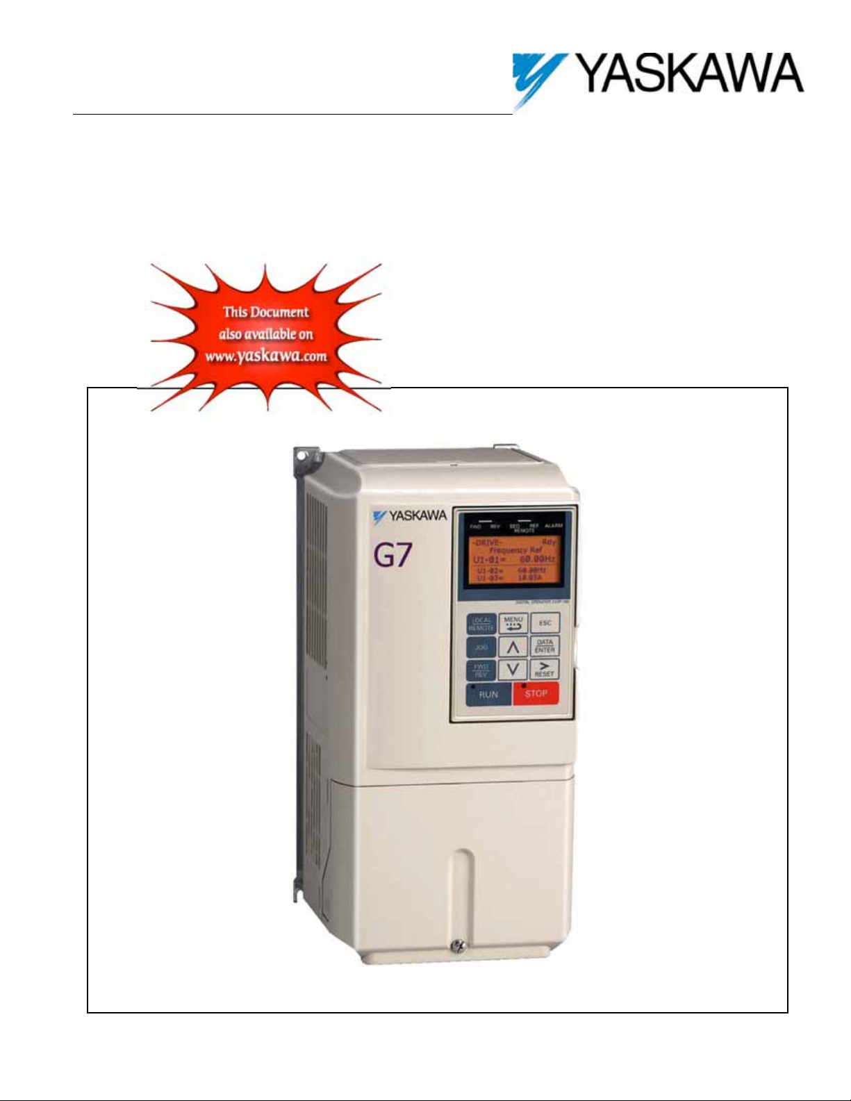
G7 Drive
Drive Model: CIMR-G7U* Document Number: TM.G7.11
Page 2

Page intentionally blank
2
Page 3

W arnings and Ca utio ns
This section provides Warnings and Cautions pertinent to this product that if not heeded, may
result in personal injury, fatality, or equipment damage. Yaskawa is not responsible for
consequences of ignoring these instructions.
WARNING
YASKAWA manufactures component parts that can be used in a wide variety of i ndustrial applications. The selection and application of
YASKAWA products remains the responsib ility of the equipment designer or end user. YASKAWA accepts no responsi b ility for the way its
products are incorpor ated into the final system design. Under no circumstances should any YASKAWA product be incor porated int o any
product or design as the e xclusive or sole safety control. Without exc eption, all controls should be designed to detect faults dyna m ically and to
fail safely under al l circumstances. All products designe d to incorporat e a component part manufactured by YASKAWA must be supplied to the
end user with appropriate warnings and i nstructions as to that part’s sa fe use and operation. Any warnings provided by YASKAWA must be
promptly provided to t he end user. YASKAWA offers an express warranty only as to the quality of it s products in conforming to standards and
specifications publi shed in the YASKAWA manual. NO OTHER WARRANTY , EXPRESS OR IMPLIED, IS OFFERED. YASKAWA
assumes no liabilit y for any personal injury, prope rty damage, losses, or claims arising from misapplication of its products.
WARNING
Read and unde rstand this ma nual before installing, ope rating, or servicing this G 7 drive. All war nings, cauti ons, and instructions must
be followed. All activity must be perf orm ed by qualified personnel. The G7 drive must be instal led accordi ng to this manual a nd local
code.
Do not connec t or disconnec t wiring while the pow er is on. Do not remove covers or touch circuit boards while the power is on. Do
not remove or insert the digital opera tor while power is on.
Before servicing, disconnect all power to the equipment. The internal capacitor remains charged even after the power supply is turned
off. Stat us indicator LEDs and D igital Operator display will be extinguished when the DC bus voltage is below 50 VDC. To prevent
electric shock, wai t at least 5 minutes after all indicators are O FF and m easure DC bus voltage and veri fy that it is at a saf e level.
Do not perf orm a withstand vol tage test on any pa rt of the unit. This equipment uses sensitive devices and may be damaged by high
voltage.
The G7 drive is not suitable for circuits capable of delivering more than the specified RMS symmetrical amperes. Install adequate
branc h short circuit protecti on per applicable codes. Refer to the specification. Fa ilure to do so may result in equipment damage a nd/or
personal injury.
Do not connec t unapproved LC or RC interference suppression fi lters, capacitors, or over voltage protection devices to the output of
the G7 drive. Capacitors may generate peak currents that exceed G7 drive specifications.
To avoid unne cessary fa ult displays, caused by contactors or output s witches placed between G7 drive and motor, auxiliary contacts
must be pr operly integra ted into the c ontrol logic circuit.
YASKAWA is not responsible for any modification of the product made by the user; doing so will voi d the warranty. This product
must not be modified.
Verif y that the rated voltage of the G7 dri ve matches the voltage of the incoming power supply before applying power.
To meet CE directives, proper line filters and pr ope r installation are requi red.
Some drawings in this ma nual may be shown wit h protective c overs or shields re moved, to describe details. These must be replaced
before operation.
Observe Electrostatic Discharge Procedures w hen handling the G7 dri ve and G7 drive com ponents to preve nt ESD damage.
The attached equipment may start unexpe ctedly upon application of power to the G7 drive. Clear all personnel fr om the G7 drive,
motor, and ma chine area pri or to applyi ng power. Secure covers, couplings, shaft keys, machine beds and all safety equipment before
ener gizing the G7 drive.
Do not attem p t to disassem ble this unit. There are no user se rviceable parts. Disassembling this unit will void any and all warranties.
3
Page 4

Introduction
This manual is intended as an overvie w of pa rameter access for the Yaskawa model G7 drive and describes how to connect the G7 dr ive to RS232, RS-422 or RS-485. Refer to the G7 Driv e Technica l Manua l ( T M .G 7 .0 1 ) for detaile d pa rameter information.
This docume n t pertains to the G7 drive. In t his document, the word “inver ter”, “ac drive” and “drive” may be used inter changeably.
For details on installation and oper ation of the G7 drive, refer to the G7 Drive Technical Manual (TM.G7.01). All manuals and support files are
available on the CD that came with the G7 drive and ar e also available for downloa d at www.yaskawa.com.
®
Modbus
All trademarks are the property of their respe ctive owners.
is a regist er ed trademark of Schneider Automation , Inc.
4
Page 5

Table of Contents
Chapter 1 - Connections....................................................................7
Connection Check Sheet................................................................................................ 8
Verify Operation.............................................................................................................. 9
G7 Drive Connections....................................................................................................10
Network Connections.....................................................................................................11
Communic at ions Par am eters.........................................................................................13
Run/Stop and Frequency Reference Source..................................................................15
Verify Communication....................................................................................................16
Chapter 2 - Message Formats.........................................................18
Protocol.........................................................................................................................20
Read Multiple Registers – Functi on Code 03H ..............................................................21
Write Single Register – Function Code 06H...................................................................23
Loop-Back Test – Function Code 08H...........................................................................25
Write Multiple Registers – Function Code 10H...............................................................27
No Response .................................................................................................................29
Error Codes...................................................................................................................29
CRC-16 Calculations.....................................................................................................30
Chapter 3 - Troubleshooting...........................................................31
General Information.......................................................................................................33
RS-232 Co mmunic at ion.................................................................................................35
RS-422/ RS- 485 Co mmunic at ion....................................................................................37
RS-422/ RS- 485 Self-Test ..............................................................................................40
Chapter 4 - G7 Drive Parameters....................................................41
Command Registers (Read/Writ e) f or Modbus RTU ......................................................42
Broadcas t R egis t ers (Write Only)...................................................................................43
Monitor Regis ters (R ead Only ).......................................................................................44
Parameter Registers (Read/Write).................................................................................52
CM090 Modbus TCP/IP Option Kit Specific Registers...................................................75
ENTER/ACCEPT Command (Write Only) ......................................................................78
Modbus Fault Decoding Table for Monitors....................................................................79
Chapter 5 - User Notes ....................................................................81
Notes.............................................................................................................................82
User Parameter Settings................................................................................................83
Hex/Dec Conversion Table............................................................................................91
5
Page 6

Notes:
6
Page 7

Chapter 1 - Connections
This chapter describes how to connect the G7 drive to a RS-232, RS-422 or RS-485 network.
Connection Check Sheet.............................................................. 8
Verify Operation............................................................................ 9
G7 Drive Connections.................................................................10
Serial Network Connections...................................................... 11
Communications Parameters.................................................... 13
Run/Stop and Frequency Reference Source............................ 15
Verify Communications.............................................................. 16
7
Page 8

Connection Check Sheet
The following is a quick reference guide to connect and configure the G7 drive for serial communications. Make a copy of this page and checkoff each item as it is completed. For detailed information please refer to the detailed sections that follow.
1: Unpack the G7 drive and verify that all com ponents are pres ent and undamaged.
2: Connect powe r to the G7 drive a nd verify that the G7 drive functi ons correctly. This includes running the G7 dri ve from the operator
keypad. Re fer to the G7 Technical Manual for information on connecti ng and operating t he G 7 drive.
3: Remove power from the G7 drive and wait for the charge lamp to be compl etely extinguished. Wait at least five additional minutes for
the G7 drive to be completely discharged. Measure the DC bus voltage and verify that it is at a safe level.
4: Connect the G7 drive to an RS-232 network. Note: It is not possible to use the drive’s key pad and an RS-232 connection at the same
time.
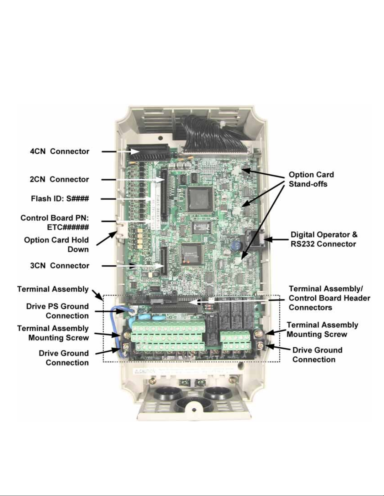
4.1: Remove the G7 drive’s operator keypad.
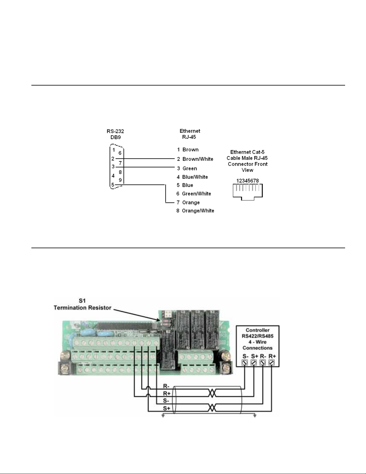
4.2: Connect the RJ-45 port on the front of the G 7 drive to the controller serial port. Refe r to Figure 1.1 - G7 D iagram for the
location of drive connectors. Use a DB9 to RJ-45 adapter with a standard Ethernet CAT-5 patch cable or use Yaskawa cable
UWR00468-2. Do NOT connect this cabl e to an Ethernet port on the controller, as damage to the controller and/or G7
drive may re su l t. R efer to Figure 1.2 – RS-232 Connections for a description of the interface cable.
4.3: V erify that the cont roller communications parameters match the G7 drive’s communications parameters. Re fer to Table 1.1
– RS-232 (RJ-45 port) Communications Parameters for a list of default G7 drive communications parameters.
4.4: Reapply power to the G7 drive.
5: Connect the G7 drive to an RS-422/RS-485 network.
5.1: Remove th e G7 drive’s te rminal cover.
5.2: Connect the controller to the S+/S- and R+/R- terminals on the G7 drive’s terminal block as shown in Figure 1.3 – RS-
422/RS-485 Connections.
5.3: If this device is either the first or last device on the network, set the network termination, S1, to the ON position.
5.4: Reapply power to the G7 drive.
5.5: Set the G7 drive communication para me ters to match t hose of the controller. Refer to Table 1.2 –Baud Rate, Table 1.3 –
Parity and Table 1.4 - RTS.
5.6: Set the node address of the G7 drive.
6: Verif y that the G7 drive a nd controller are communicating and that the exchanged data is valid.
8
Page 9
Verify Operation
Connect powe r to the G7 drive a nd verify that the G7 drive functions properly. This includes running the G7 drive from the operat or keypad.
Refer to the G7 drive Technical Manual for infor ma tion on connecting and operating the G7 drive.
Remove power from the G7 drive and wait for the charge lamp to be completely extinguished. Wait at least five additional minutes for the G7
drive to be completely discharged. Measure the DC bus voltage and verify that it is at a safe level.
Remove the ope rator keypad and terminal cover.
Figure 1.1 G7 Connection Diagram
9
Page 10
G7 Drive Connections
Figure 1.2 G7 Drive Connecti ons
10
Page 11
Network Connections
The following describes how to connect the G7 drive to an RS-232, RS-422 or RS-485 network. For detailed information please refer to the
appropriate sections of this manual or the G7 drive Technical Manual.
RS-232 Network
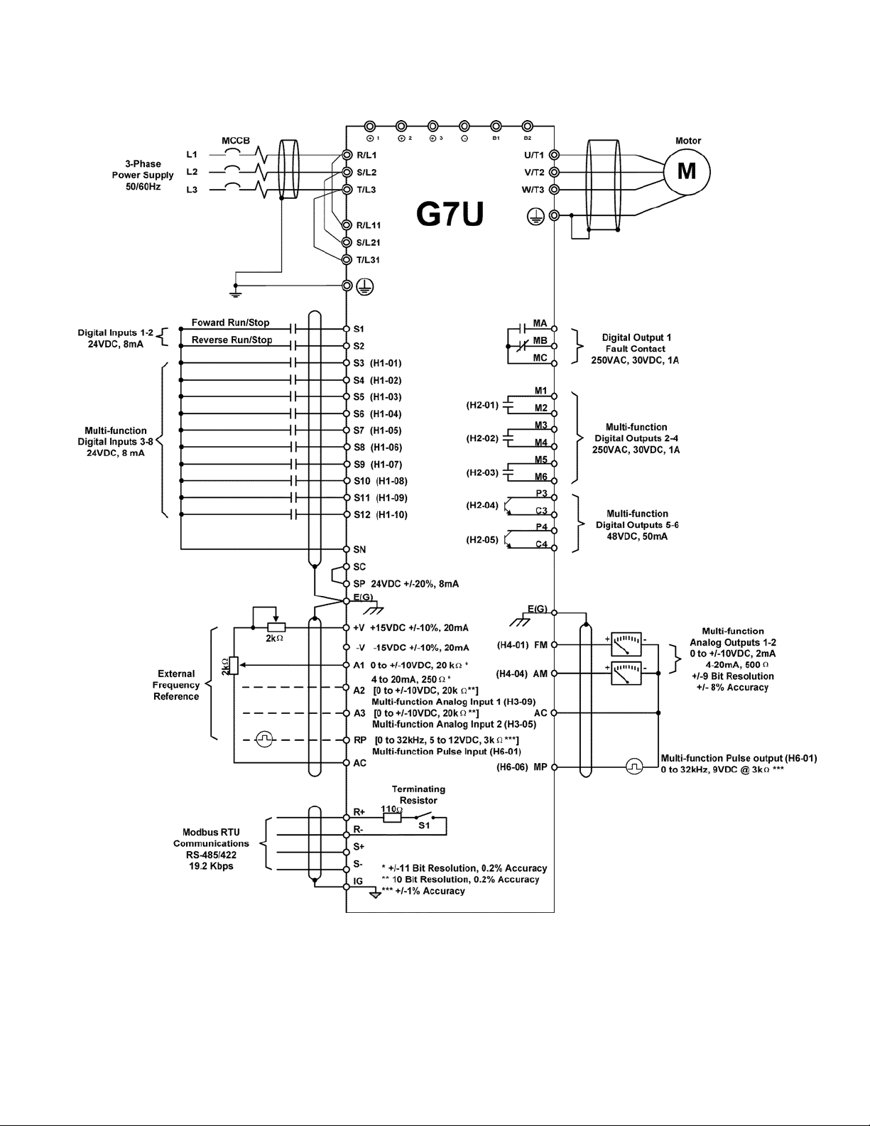
The RS-232 network is a single ended network wit h limited data trans mission rates and cable lengt hs. The G7 drive RS- 232 data transmission is
fixed at 9600bps, no parity, 8 data bits and 1 st op bit. The maximum cable length is 50 ft ( 16 m). It is recommende d that Yaskawa cable
UWR00468-2 be used. Note: It is not possible to use the drive’s keypad and an RS-232 connection at the same time.
Figure 1.3 RS-232 Network Connection
RS-422/RS-485 4-Wire Network
RS-422/RS-485 4-wire net w orks allow for longer cable lengths, maximum 4000 ft (1200 m ), and are more im m une to noise than RS-232
networ ks because of thei r balanced li ne drivers. RS-422/RS-485 4-wire communicati on does not requir e RTS (request to send) control. See
parameter H5-07. Set the Termination Resistor S1 sw itch to ON (slide the switch to the right) fo r each RS-422 device and the last RS-485
device on the network.
Figure 1.4 RS-422/RS-485 4-Wire Network Connection
11
Page 12
RS-485 2-Wire Network
RS-485 2-wire networks can be either single or multi-drop networks, with each slave de vice on the networ k assigned a unique nod e address. A
maximum of 31 devices may reside on any network segment bef ore a repeater is required. The ma ximum segment le ngth is 4000 ft (1200 m).
Set the T erm ination Resi stor S1 switch t o O N (s lide the switch to the right) on the last device on the network. RS- 485 2-wire communication
requires RTS (request to send) control. See parameter H5-07.
Figure 1.5 RS-485 2-Wire Network Connection
12
Page 13

Communication Parameters
The following communicati ons parameters affect communication over RS-232, RS-422 and RS-485 networks. The RS- 232 communication
paramet ers are fixe d. In addition, the node address is ignored when comm unicating via RS-232.
H5 group communication parameters can onl y be changed via the drive keypad.
Note: Drive power must be cycled for changes to H5 Group parameter s to be recognize d.
RS-232 Communication
The RS-232 co m m unications param eters are fixed at the values show n below. Although the node address is ignore d, the master when
communicating to the G7 drive in this method typically uses a node address of 1.
Table 1.1 RS-232 (RJ-45 port) Communi cati on Parameters
Value Description
Baud rate 9600
Parity None
Stop Bits 1
Node Address N/A
RS-422/RS-485 Communication
Node Address – H5-01. The node address is set thr ough G 7 drive paramete r H5-01. When communi cating via RS- 422 or RS-485, a
unique node address between 0 and 20h (32 decima l), inclusive, must be entered. The defa ult G7 drive addres s is 1Fh (31 decimal).
The addres s is always ente red as a hexadecimal number (ref er to the conversion chart in Chapter 4). A ddress 0 is typica lly reserved for
global me ssages.
Baud Rate – H5-02. Select the baud rate that matches the controller’s communica tion configur ation.
Table 1.2 Baud Rate – Parameter H5-02
Value Description
0 1200bps
1 2400bps
2 4800bps
3 9600bps (Default Setting)
4 19,200bps
Parity – H5-03. Select t he parity that matc hes the controller’s communi cation conf iguration.
Table 1.3 Parit y – Param eter H5-03
Value Description
0 None (Default Setting)
1 Even
2 Odd
13
Page 14

Communication Fault (CE) Response Selection – H5-04. Select the drive operation method when a communic ation fault (CE)
occurs . See parameter H5-05 also.
Table 1.4 Communicati on Fault Response Sel ection – Parameter H5-04
Value Description
0 Ramp to Stop (Fault)
1 Coast to Stop (Fault)
2 Fast Stop (Fault)
3 Alarm Only (Alarm) (Default Setting)
4 Run at D1-04 frequency
Communication Fault (CE) Detection Selection – H5-05. Selects whether the communication fa ult (CE) is monitor ed. Please note
that either B1-01 or B1-02 must also be set to a 2 (Serial Communication) for fault monitoring to occur. If the CE fault is enabled, the
G7 will flash CALL on the keypad after power up until a message is rec eived. The dri ve w ill trip and respond according to H5-04 if
communication is lost (a message is not received) for more than 2 seconds after s uccessful communication has been initiat ed.
Table 1.5 Communicati on Fault Det ecti on Selection – Parameter H5-05
Value Description
0 Disabled (Default Setting)
1 Enabled
Serial Com munication Send Delay – H5-06. A delay can be inserted bef ore the G7 drive responds to a command message. This
allows for slower communication devices to switch their transceiver state in order to get ready to receive a message. A value of 5 ~ 65
ms can be inserted, with 5 ms being the default.
RTS Control – H5-07. This paramete r determines whether RTS is cont inually asserted (disabled) or asserted only duri ng send
(enabled). RTS must be enabl ed for use with RS- 485 2-wire communication.
Table 1.6 RTS Control – Parameter H5-07
Value Description
0 Disable (always ON) (Default Setting)
1 Enable (ON only during send) (Use this s e tting for RS-485 2-wire systems)
14
Page 15

Run/Stop and Frequency Refere nce
The Run/Stop and Frequency Reference commands can originate from:
Serial communication (Built-in Modbus: Keypad or R+/-, S+/- T erm inals)
Keypad (Digital Operator)
Terminal Strip
Option Card
Paramet er B1-01 (Run/Stop Method Selection) allows the selection of t he origin of the Run/Stop command. Parameter B1-02 (Re ference
Selection) allows the selection of the origin of the Frequency Reference com m and. The Run/Stop and Frequency Reference commands may
have different origi ns.
For exampl e, the Run/Stop co m ma nd m ay be set to Termina ls (B1-01=1) while the Freque ncy Reference command may be set to Serial
Communicat ion (B1-02=2).
Run/Stop Source
Table 1.7 Run/Stop Method Selecti on
B1-01 Operation Method Selection (Run/Stop)
0 Keypad
1 Terminal Strip (Default Setting)
2 Serial Communication (Built-in Modbus: Keypad or R+/-, S+/- Terminals)
3 Option Card (EtherNet/IP, Modbus TCP/IP, DeviceNet, Profibus DP, LonWorks, etc.)
4 Pulse Input (RP Terminal)
Frequency Reference Source
Table 1.8 Frequency Ref erence Source Selection
B1-02 Frequency Reference Selection
0 Keypad
1 Terminal Strip (Default Setting)
2 Serial Communication (Built-in Modbus: Keypad or R+/-, S+/- Terminals)
3 Option Card ( EtherNet/ IP, Modbus TCP/IP, DeviceNet, Profibus D P, LonWorks, etc. )
15
Page 16

Verify Communication
The following is a quick ref erence guide for serial communications to the G7 drive. Make a copy of this page and check-off eac h item as it is
completed. For detailed information please refer to the detailed sections that follow.
1: RS-232 Communication.
1.1: Verify that the correct cable is used to connect the controller to the G7 drive.
1.2: V erify that the controller is set f or RS-232 communica tion and that the communication cable is connected to the c orrect
communication port.
1.3: Record the control ler communication parameters.
Baud Rate
1.4: Record the G7 drive comm unication para m eters (H5-02, H5-03, H5-07) .
Baud Rate
1.5: Verify that the communication parameters match.
2: RS-422/RS-485 Communication.
2.1: V erify that the G7 drive is connected correctly.
2.2: V erify that the controller is set f or RS-422/RS-485 c om munications and that the communications cable is connected to
the correct communica tions port.
2.3: Record the control ler communications parameters.
Baud Rate
2.4: Record the G7 drive comm unication para m eters (H5-01, H 5-02, H5-03, H5-07).
Baud Rate
Parity Data Bits Stop Bits 1
Parity Data Bits Stop Bits 1
Parity Data Bits Stop Bits 1
Parity Data Bits Stop Bits 1
2.5: Verify that the communication parameters match.
2.6: Verify that parameter H5-07 (RTS) is set to enable.
2.7: V erify that paramet er H5-01 (Node A ddress) is set to the correct, unique, hexadecimal value and that it matches the
node address required by the controller.
Controller Node Address
G7 Drive Node Address
16
Page 17

3: Send a command message to the G7 drive fr om t he controller and verify the data of the comma nd and response messages.
3.1: Verify the conten ts of th e com mand message.
Notes:
[
[
[
[
3.2: Verify the contents of the response message.
[
[
[
[
] [ ] [ ] [ ] [ ] [ ] [ ] [ ] [ ] [ ]
] [ ] [ ] [ ] [ ] [ ] [ ] [ ] [ ] [ ]
] [ ] [ ] [ ] [ ] [ ] [ ] [ ] [ ] [ ]
] [ ] [ ] [ ] [ ] [ ] [ ] [ ] [ ] [ ]
] [ ] [ ] [ ] [ ] [ ] [ ] [ ] [ ] [ ]
] [ ] [ ] [ ] [ ] [ ] [ ] [ ] [ ] [ ]
] [ ] [ ] [ ] [ ] [ ] [ ] [ ] [ ] [ ]
] [ ] [ ] [ ] [ ] [ ] [ ] [ ] [ ] [ ]
17
Page 18

Notes:
18
Page 19

Chapter 2 - Message Formats
This chapter provides information on the message (telegram) contents and configuration.
Protocol....................................................................................... 20
Read Multiple Registers – Function Code 03H......................... 21
Write Single Register – Function Code 06H............................. 23
Loop-Back Test – Function Code 08H...................................... 25
Write Multiple Registers – Function Code 10H........................ 27
No Response............................................................................... 29
Error Codes................................................................................. 29
CRC-16 Calculation .................................................................... 30
19
Page 20

Protocol
The parame ter access met hod supported by the G 7 drive is a subset of the Modbus♦ communication protocol, which Yaskawa refers to as
MEMOBUS. The G7 drive supports Modbus functions 3, 6, 8 and 10h. The message format varies depending upon the f unction code of the
message. For each function code, there is a command message from the master and a response me ssage from the slave. The following sections
review the format of the command and response messages for each funct ion.
Message Functions Supported
The following table lists the Modbus functi on codes availa ble and their mi nimum and m aximum byte lengths.
Table 2.1 Supported Function Codes
Function Code Function
3h (3 dec) Read Multiple Registers 8 8 7 21
6h (6 dec) Write Single Register 8 8 8 8
8h (8 dec) Loop-Back Tes t 8 8 8 8
10h (16 dec)
Write Multiple Re g iste rs 11 25 8 8
Minimum (bytes) Maximum (bytes) Minimum (bytes) Maximum (byt es )
Command Message Response Message ( N ormal)
20
Page 21

Read Multiple Registers – Function Code 03H
The Read Multiple Register function is used to read the contents of from 1 to 8 consecutive registers. The formats of the read command and
response m essages are shown below.
Read Multiple Registers Command Message
Table 2.2 Read Command Message
Description Data
Starti ng Register
Each G7 dri ve slave address is set via parameter H5-01. Vali d slave address es must be in the ra nge of 1 ~ 20 hex (1 ~ 32 dec) and entered as a
hexadec imal number. No two slaves may have the same address . The master addresses the slave by placing the slave address in the Slave
Address field of the message. In the command message above, t he slave is addr essed at 02h. Broadcast address 0 is not valid for register re ad
commands.
Slave Address 02h
Function Code 03h
Upper 00h
Lower 20h
Quantity
CRC-16
Upper 00h
Lower 04h
Upper 45h
Lower F0h
The function code of this mes sage is 03h (read multiple registers) .
The starting regist er is the addres s of the first register to be read. In the command message a bove the starting register a ddress is 20h (0020h).
The quantity indicates how many consecu tive registers are to be read. The quantit y ma y range from 1 to 8 registers. If an invalid quantity is
entere d, error code 03h is returned i n a fault response message. I n this example, four consecutive register s are to be read: 20h, 21h, 22h and 23h.
A CRC-16 value is generated from a calculation including the message sla ve address, function code, sta rting register and quanti ty. The
procedure for calculating a CRC-16 is described at the end of this chapter. When the slave receives the command message it calculates a CRC16 value and compa res it to the CRC-16 of the command message. If the two CRC-16 values are identical and the Slave Addr ess is correct, the
slave process es the command message. If the two CRC- 16 values are not identica l, the slave will discard the command message and not
respond.
If the com ma nd me ssage has a valid slave address, function code, starting register, and quantity , the slave wil l respond with a normal response
message. If the command message has an invalid function code, starting register, and/or quantity, the slave will respond with a fault response
message. If the command message has an i nvalid slave addr ess or CRC-16, no response will be returned.
21
Page 22
Read Multiple Registers Normal Response Message
Table 2.3 Read Normal Response Message
Description Data
Starti ng Register
Next Register
Next Register
Last Register
The normal response message contains the same slave address and funct ion code as the command message, indicating to the master which
specific slave is responding and to what type of function it is responding.
Slave Address 02h
Function Code 03h
Number of Data Bytes 08h
Upper 17h
Lower 70h
Upper 17h
Lower 70h
Upper 01h
Lower 09h
Upper 00h
Lower 00h
CRC-16
Upper 38h
Lower ACh
The number of data bytes is t he num ber of data bytes returned in t he response message. The number of da ta bytes is actually the number of
regist er s read time s 2, since th er e ar e tw o by te s of data in each register.
The starting register is the address of the first register read.
The data section of the response message contains the data for the registers' requested re ad, in this case registers 20h, 21h, 22h and 23h. Their
data is 20h = 1770h, 21h = 1770h, 22h = 0109h and 23h = 0h.
Read Multiple Registers Fault Response Message
Table 2.4 Read Fault Response Message
Description Data
The fault response message contai ns the same slave address as the command message, indicating to the master, which slave is responding.
The function code of a fault response message is the logical OR of 80h and the original function code of 03h. This indicates to the master that
the message is a fault response message, instead of a normal response message.
Slave Address 02h
Function Code 83h
Error Code 02h
CRC-16
Upper 30h
Lower
F1h
The error code indicates w h ere the err or occurred in the com mand message. The value of 02h in the error code field of this fault response
message indicates that the command me ssage requested data be read from an invalid register. Refer to section Error Codes, Table 2- 14, for
more info rmation on retu rned erro r co d es.
22
Page 23

Write Single Register – Function Code 06H
The Write Single Register function allows the writing of data to one regi ster only.
Write Single Register Command Message
Table 2.5 Write Command Message
Description Data
Register Address
Each G7 dri ve slave address is set via parameter H5-01. Vali d slave address es must be in the ra nge of 1 ~ 20 hex (1 ~ 32 dec) and entered as a
hexadec imal number. No two slaves may have the same address . The master addresses the slave by placing the slave address in the Slave
Address field of the message. In the command me ssage above, t he slave is addr essed at 01h. Broadcast address 0 is valid for register write
commands.
Slave Address 01h
Function Code 06h
Upper 00h
Lower 01h
Data
CRC-16
Upper 00h
Lower 03h
Upper 98h
Lower H0B
By setting the slave address to zero (0) in the command message, the master can send a message to all the slaves on the network simultaneously.
This is called simultaneous broadcasting. In a simultaneous broadcast message there is no response message.
The function code of this mes sage is 06h (writ e single regi ster).
In the command message above the register address is 01h (0001h).
The data section contains the data to be written.
A CRC-16 value is generated from a calculation including the message slave address, function code, starting register, quantity, Number of Data
Bytes, and all register data. The procedure for calculating a CRC-16 is described at the end of this chapter. When the slave receives the
command message it calculates a CRC-16 value and compares it to the CRC-16 of the command messa ge. If t he two CRC-16 values are
identical and the slave address is correct, the slave processes the command messa ge. If the two CRC-16 values are not identical, the slave will
discard the command messa ge and not respond.
If the com ma nd me ssage has a valid slave address, function code, regis ter address and data, the sla v e w ill respond wi th a normal response
message. If the command message has an invalid function code, regi ster addres s and/or data, the slave will respond with a fault response
message. If the command message has an i nvalid slave addr ess or CRC-16, no response will be returned.
23
Page 24
Write Single Register Normal Response Message
Table 2.6 Write Register Normal Response Message
Description Data
Register Address
The normal response message contains the same slave address, funct ion code, re gister address and data as the command message, indicating to
the master which slave is responding and t o w hat type of function it is responding.
In the response message above the register address is 01h (0001h).
Slave Address 01h
Function Code 06h
Upper 00h
Lower 01h
Data
CRC-16
Upper 00h
Lower 03h
Upper 98h
Lower 0Bh
Write Single Register Fault Response Message
Table 2.7 Write Register Faul t Response Message
Description Data
The faul t response message contai ns the same slave address as the command message, indicating to the master which slave is responding.
The function code of a fault response message is the logical OR of 80h and the original function code of 06h. This indicates to the master that
the message is a fault response message, instead of a normal response message.
The error code indicates w h ere the err or occurred in the com mand message. The value of 21h in the error code field of this fault response
message indicates that the command me ssage data to be written was invalid for that register . Refer to the sec tion Error Codes, Table 2-14, for
more info rmation on retu rned erro r co d es.
Slave Address 01h
Function Code 86h
Error Code 21h
CRC-16
Upper 82h
Lower 78h
24
Page 25

Loop-Back Test – Function Code 08H
The Loop-Bac k Test is used to ver ify that the com m unications pa rameters for the G7 drive have been set correctly and that the connection i s
correct. The message should be constructed exactly as shown below. If everything is set and connected correctly, the received response will
match the response shown below.
Loop-Back Test - 08h
The Loop-Back test function (08h) is used for checking signal transmiss ion between maste r and slaves. The com ma nd m essage format is shown
below.
Table 2.8 Loop-Back Command Message
Description Data
Slave Address 01h
Function Code 08h
Test Code
Data
CRC-16
Upper 00h
Lower 00h
Upper A5h
Lower 37h
Upper DAh
Lower 8Dh
Each G7 dri ve slave address is set via parameter H5-01. Vali d slave address es must be in the ra nge of 1 ~ 20 hex (1 ~ 32 dec) and entered as a
hexadec imal number. No two slaves may have the same address . The master addresses the slave by placing the slave address in the slave
address field of the message. In the co m ma nd m essage above, the slave is addressed at 01h. Broadcast address 0 is not valid for Loop-Back test
commands.
The function code of this message is 08h (Loop- Back test).
The test code must be set to 0000h. This function specifies that the data passed in the command message is to be returned (looped back) in the
response message.
The Data sec tion contains arbitrary values.
A CRC-16 value is generated from a calculation including the message slave a ddress, funct ion code, test code, and data. The pr ocedure for
calculating a CRC-16 is described at the end of this chapter. When the slave receives the command me ssage it calculates a CRC- 1 6 value and
compares it to the CRC- 16 of t he comma nd messa ge. If the two CRC-16 values are identical and the Slave Address is correct, the slave
processes the command mes sage. If the two CRC-16 values are not identical, the slave will disc ard the command mes sage and not respond.
If the comma nd me ssage has a vali d slave address, function code, test code, data and CRC-16, t he slave will respond with the normal response
message. If the command message has an invalid function code, tes t code, and/or data, the slav e w ill respond wit h a fault response me ss ag e. If
the command message has an invalid slave address or CRC-16, no response will be returned.
25
Page 26

Loop-Back Normal Response
The normal Loop-Back Test response is identical to the command message.
Table 2.9 Loop-Back Normal Response Message
Description Data
Slave Address 01h
Function Code 08h
Test Code
Data
CRC-16
Upper 00h
Lower 00h
Upper A5h
Lower 37h
Upper DAh
Lower 8Dh
Loop-Back Fault Response
Table 2.10 Loop-Back Fault Response Message
Description Data
Slave Address 01h
Function Code 88h
Error Code 01h
CRC-16
Upper 87h
Lower C0h
The faul t response message contai ns the same slave address as the command message, indicating to the master which slave is responding. The
function code of a fault res ponse message is the logical OR of 80h and the origin al function code of 08h. This indicates to the master that the
message is a fault response message, instead of a normal response message.
The error code indicates where the error occurred in the command message. Refer to the section Error Codes, Table 2-14, for more inf o rm at io n
on return ed error cod e s.
26
Page 27

Write Multiple Registers – Function Code 10H
The Write Mul tiple Register function allows the writi ng of data to from 1 t o 16 consecutive re gisters.
Write Multiple Registers Command Message
Table 2.11 Write Command Message
Description Data
Starti ng Register
First Register Data
Next Register Data
Slave Address 01h
Function Code 10h
Upper 00h
Lower 01h
Quantity
Number of Data Bytes 04h
CRC-16
Upper 00h
Lower 02h
Upper 00h
Lower 01h
Upper 02h
Lower 58h
Upper 63h
Lower 39h
Each G7 dri ve slave address is set via parameter H5-01. Vali d slave address es must be in the ra nge of 1 ~ 20 hex (1 ~ 32 dec) and entered as a
hexadec imal number. No two slaves may have the same address . The master addresses the slave by placing the slave address in the Slave
Address field of the message. In the command me ssage above, t he slave is addr essed at 01h. Broadcast address 0 is valid for register write
commands.
By setting the slave address to zero (0) in the command message, the master can send a message to all the slaves on the network simultaneously.
This is called simultaneous broadcasting. In a simultaneous broadcast message there is no response message.
The function code of this mes sage is 10h (writ e m ultiple registers).
The starting register is the address of the first register to be written. In the command message above the starting register address is 01h (0001h).
The quantity indicates how m any consecuti ve registers are to be written. The quantity may range fr om 1 to 16 registers. If an invalid quantity is
entere d, error code of 03h is returne d in a fault respons e m essage. In this command messa ge there are t w o consecutive registers to be written:
0001h (Oper ation Command) and 0002h ( F requency Ref erence).
The number of data bytes is t he num ber of bytes of dat a to be written. The number of data byt es is actual ly the quantity multiplie d by 2, since
there are two bytes of data in each register.
The Data section contains the data for each register to be written in the order in which they are to be written.
A CRC-16 value is generated from a calculation including the message slave address, function code, starting register, quantity, Number of Data
Bytes, and all register data. The procedure for calculating a CRC-16 is described at the end of this chapter. When the slave receives the
command message it calculates a CRC-16 value and compares it to the CRC-16 of the command messa ge. If t he two CRC-16 values are
identical and the slave address is correct, the slave processes the command messa ge. If the two CRC-16 values are not identical, the slave will
discard the command messa ge and not respond.
If the com ma nd me ssage has a vali d slave address, function code, starting register, quantity, number of data byte s and data, and the slave will
respond with a normal response message. If the command message has an invalid function code, starting register, quantity, Number of Data
Bytes a nd/or data, the slave will respond with a fault response message. If the command message has an invali d slave address or CRC-16, no
response w ill be returned.
27
Page 28
Write Multiple Registers Normal Response Message
Table 2.12 Write Registers Normal Response Message
Description Data
Starti ng Register
The normal response message contains the same slave address, function code, starting register and quantity as the command message, indicating
to the mast er which slave is responding and to what type of f unction it is responding.
The starting register is the address of the first register written. In the response message above the starting register address is 01h (0001h).
The quantity indicates how m any consecuti ve registers were written. In this case the quantity is 2.
Slave Address 01h
Function Code 10h
Upper 00h
Lower 01h
Quantity
CRC-16
Upper 00h
Lower 02h
Upper 10h
Lower 08h
Write Multiple Registers Fault Response Message
Table 2.13 Write Registers Fault Response Message
Description Data
The faul t response message contai ns the same slave address as the command message, indicating to the master which slave is responding.
The function code of a fault response message is the logical OR of 80h and the original function code of 10h. This indicates to the master that
the message is a fault response message, instead of a normal response message.
The error code indicates w h ere the err or occurred in the com mand message. The value of 02h in the error code field of this fault response
message indicates that the command me ssage requested data to be written to an invalid register . Refer to the section Error Codes, Table 2-14,
for more information on returned error codes.
Slave Address 01h
Function Code 90h
Error Code 02h
CRC-16
Upper CDh
Lower C1h
28
Page 29

No Response
The slave disregards t he command message and does not return a response message in the follow ing cases:
1. In broadcasting of data (slave addres s is 0), all slaves execute, but do not respond.
2. When a communicati on error (overrun, fr aming, parity, or CRC-16) is detected in the command message.
3. When the slave address in the command message does not coincide with the address set in the slave.
4. When it ta kes longer than 2 seconds to send a mes sage.
5. When the time interval between characters exceeds 3.5 ms.
6. When the command message data length is not proper.
Error Codes
Table 2.14 Fault Codes
Code Fault Description
1 F unction Error Invalid or unsupported function code in command message
2 Invalid Regis ter Invalid regis ter address
3 Invalid Number of Registers Invalid command message quantity
21 Data Limits Exceeded The write command message data is out of range for the requested r e gister
22 Write Fai lure The register to be written is write protected
29
Page 30

CRC-16 Calculation
The last two bytes of a message contain the CRC-16 ( C yclical Redunda ncy Check). The CRC-16 is one method for verifying the validity of the
message contents and is part of the protocol. The CRC-16 field checks the contents of the entire message, regardless of any parity check method
used for the individua l characters of the message.
The CRC-16 fiel d is a 16- bit binary value consisting of two 8-bit bytes. The CRC-16 value is calculated by t he transmitting device, which
appends the CRC-16 to the messa ge. The receiving device recal culates a CRC-16 dur ing receipt of the message, and compares this calculated
value to the value received in the transmitted CRC-16 field. If the two values are not equal, the entire message is invalid.
Detailed examples of a CRC-16 generati on using Quick Basic and C are shown below.
CRC-16 Calculation Example in Basic
crcsum# = &HFFFF&
crcshift# = &H0&
crcconst# = &HA001&
CLS
PRINT “*********** ****************************************”
PRINT
PRINT “ CRC-16 calculator”
PRINT
PRINT “*********** ****************************************”
PRINT “If e ntering data in hex, preceed the data with ‘&H’”
PRINT “ Example: 32decimal = 20hex = &H20”
PRINT “*********** ****************************************”
PRINT
INPUT “Enter the number of bytes in the message: “, maxbyte
FOR bytenum = 1 TO maxbyte STEP 1
PRINT “Enter byte “; bytenum; “:”:
INPUT byte&
byte& = byte& AND &HFF&
crcsum# = (crcsum# XOR byte&) AND &HFFFF&
FOR shift = 1 TO 8 STEP 1
crcshift# = (INT(crcsum# / 2)) AND &H7FFF&
IF crcsum # A ND &H1& TH EN
crcsum# = crcshift# X O R cr cco nst#
ELSE
crcsum# = crcshift#
END IF
NEXT shift
NEXT bytenum
lower& = crcsum# AND &HFF&
upper& = (INT(crcsum# / 256)) AND &HFF&
PRINT “Lower byte (1
PRINT “Upper byte (2
st
) = “, HEX$(lower&)
nd
) = “, HEX$(upper&)
30
Page 31

CRC-16 Calculation Example in C
void getMBCRC(char *, int, char *) // function prototype
void getMBCRC(char *buf, int bufLen, char *cr c) { // Function name and par am eter list returning a void
// *buf pointer to character array used to calcula te CRC
// bufLen number of characters to calculate CRC for
// *crc pointer to the array that contains the calculated CRC
unsigned long crc_0 = 0xffff; // Declare and initialize variables
unsigned long crc_1 = 0x0000; // Declare and initialize variables
int i,j; // Declare and initialize variables
for (i=0; i<bufLen; i++) { // Loop through characters of input array
crc_0 ^= (( unsigned long) buf[i] & 0x00ff); // XOR current character w ith 0x00ff
for (j=0;j<8;j++) { // Loop through characters bits
crc_1 = (crc_0 >> 1) & 0x7fff; // shift result right one place and store
if (crc_0 & 0x0001) // if pre-shifted value bit 0 is set
crc_0 = (crc_1 ^ 0xa001); // XOR the shift ed value with 0xa 001
else // if pre-shifted value bit 0 is not set
crc_0 = crc_1; // set the pre-shifted value equal to the shifted value
} // End for loop - Loop through characters bits
} // End for loop - Loop through c haracters of input array
crc[0] = (unsigned char)((crc_0/256) & 0x00ff); // Hi byte
crc[1] = (unsigned char)(crc_0 & 0x00ff); // Lo byte
return; // Return to calling function
} // End of CRC calculation function
31
Page 32

Notes:
32
Page 33

Chapter 3 - Troubleshooting
This chapter describes basic troubleshooting methods for serial communication.
General Information ................................................................... 34
RS-232 Communication.............................................................. 35
RS-422/RS-485 Communication ................................................ 37
RS-422/RS-485 Self-Test ........................................................... 40
33
Page 34

General Information
Please fill in the infor ma tion on this and the following pa ges prior to contacting cust ome r support. If customer suppor t is necessary, please have
the information below available.
1: G7 Drive Model CIMR-_____
2: Input__
3: Serial Number_______________
VAC____Hz 5: Software ID (U1-14) __________________
4: Control Board ETC-_____
6: Initialization Type (2 or 3 wire control) _____________
Please provide a sketc h of the network in t he space below.
34
Page 35

RS-232 Communication
The following is a quick reference guide for troubleshooting RS-232 communication to the G7 drive. Make a copy of the following pages and
check-off each item as it is completed. For detailed information on the RS-232 standard please refer to EIA RS-232-C or later revision. For
information on the G7 dri ve RS-232 interface, refer to previous sections of this manual.
1: For RS-232 communicati on.
1.1: Verify that the correct cable is used to connect the controller to the G7 drive.
1.2: V erify that the controller is set f or RS-232 communica tion and that the communication cable is connected to the c orrect
communication port.
1.3: Record the control ler communications parameters.
Baud Rate
1.4: Record the G7 drive’s communication parameters (H5-02, H5-03, H5-07).
Baud Rate
1.5: Verify that the communication parameters match.
2: Check the controller RS-232 wiring requirement s.
2.1: CTS (Clear to Send)/RTS (Rea dy to Send) jumper required on the controller end?
2.2: DTR (Data Terminal Ready)/DSR (Data Set Ready)/RLSD (Receive Line Signal Detector) jumper required on the
controller end?
2.3: TXD (Transmit Data) /RXD (Receive Data) connecti ons are made correctly?
3: Send a message from t he controller to the G7 drive.
3.1: Connect an oscilloscope between the G 7 drive RXD and GND.
3.1.1: Verify that the me ssage pulse train exists and contains the correct number of pulses. Re fer to the chapter
Message Formats for information on the message contents.
Parity Data Bits Stop Bits 1
Parity Data Bits Stop Bits 1
3.1.2: Verify that the signal levels adhere to the RS-232 standar d.
3.2: Insert a data analyzer in the RS-232 ci rcuit and capt ure the message sent by the controller in a he xadecimal format.
Record the command message below.
[
[
[
[
] [ ] [ ] [ ] [ ] [ ] [ ] [ ] [ ] [ ]
] [ ] [ ] [ ] [ ] [ ] [ ] [ ] [ ] [ ]
] [ ] [ ] [ ] [ ] [ ] [ ] [ ] [ ] [ ]
] [ ] [ ] [ ] [ ] [ ] [ ] [ ] [ ] [ ]
35
Page 36

3.3: V erify that the contents of the messa ge adhere to the pr otocol format as described previously.
3.3.1: Verify that the node address is valid.
3.3.2: Verify that the function code is valid.
3.3.3: Verify that the register address is valid.
3.3.4: Verify that the num ber of data bytes is valid.
3.3.5: Verify that the CRC is correctly calculated.
3.3.6: Verify that t he me ssage requires a response.
4: Verify the contents of the response message.
4.1: Connect an oscilloscope between the contr oller RXD and GND.
4.1.1: Verify that the me ssage pulse train exists and contains the correct number of pulses. Re fer to the chapter
Message Formats for information on the message contents.
4.1.2: Verify that the signal levels adhere to the RS-232 standar d.
4.2: Capture the response me ssage sent by the controller in a hexadecimal format and recor d it below.
[
[
[
[
4.3: V erify that the contents of the messa ge adhere to the pr otocol format as described previously.
] [ ] [ ] [ ] [ ] [ ] [ ] [ ] [ ] [ ]
] [ ] [ ] [ ] [ ] [ ] [ ] [ ] [ ] [ ]
] [ ] [ ] [ ] [ ] [ ] [ ] [ ] [ ] [ ]
] [ ] [ ] [ ] [ ] [ ] [ ] [ ] [ ] [ ]
4.3.1: Verify that the node address is valid.
4.3.2: Verify that the function code is valid.
4.3.3: Verify that the num ber of data bytes is valid.
4.3.4: Verify that the register address is valid.
4.3.5: Verify that the CRC is correctly calculated.
36
Page 37

RS-422/RS-485 Communication
The following is a quick reference guide for troubleshooting RS-422/RS-485 communicati on to the G7 drive. Ma ke a copy of the following
pages a nd check-off eac h item as it is completed. For detailed information on the RS-422/RS-485 standard ple ase refer to EIA RS-422-A or later
revision. For information on the G7 dri ve RS-422/RS-485 interface, refer to previous sections of this ma nual.
1: For RS-422/RS-485 communic ations.
1.1: Verify that the correct cable is used to connect the controller to the G7 drive.
1.2: V erify that the controller is set for RS-422 or RS-485 comm unications and that the communications cable is connected
to the correct communications port.
1.3: Record the control ler communication parameters.
1.4: Verify that the polarity of the signal wires is correct (+ to + and - to -).
Baud Rate
1.5: Record the G7 drive comm unication para m eters (H5-01, H 5-02, H5-03, H5-07).
Baud Rate
1.6: Verify that the communication parameters match.
1.7: For RS-485 2-wire networks only, verify that G7 drive param eter H5-07 (RTS) is set to 1 (Enable ).
1.8: V erify that G7 drive parameter H5-01 (Node Address) is set to the correct, unique, hexadecimal value and that it
matches the node address required by the controller.
2: Check the controller RS-422/RS-485 wiring requirements.
2.1: The controller transmit termi nals are connected to the G7 drive receive term inals and the receive terminals connected to
the G7 dr ive trans mit terminals.
2.2: The transmit and rece ive connection polarities are correct.
2.3: The controller either assert s R T S w hen transmitting or utilizes send detect circuitry.
2.4: The network is terminated only at the beginning and end of each network segment.
Parity Data Bits Stop Bits 1
Parity Data Bits Stop Bits 1
2.5: There are no m o re than 31 device s on any network segment, incl uding the contro ller and repeater.
3: Verify that the G7 drive passes the self-test as described in the following section.
37
Page 38

4: Send a message from t he controller to the G7 drive.
4.1: Connect an oscilloscope between the G 7 drive’s R+ and R- termi nals for RS-422/RS-485 4-wire netw orks or between
terminals R+/S+ and R-/S- for RS-485 2-wire netw orks.
4.1.1: Verify that the message pulse train exists a nd contains the c orrect number of pulses. Refer to the chapter
4.1.2: Verify that the signal levels adhere to the RS-422/RS-485 standar d.
4.2: Insert a data analyzer in the RS-422/RS-485 circui t and capture the me ssage sent by the controller in a hexadecimal
format. Record the command message below.
[
[
[
[
4.3: V erify that the contents of the message adhere to the M odbus format as describe d previously.
4.3.1: Verify that the node address is valid.
4.3.2: Verify that the function code is valid.
4.3.3: Verify that the register address is valid.
Message Formats for information on the message contents.
] [ ] [ ] [ ] [ ] [ ] [ ] [ ] [ ] [ ]
] [ ] [ ] [ ] [ ] [ ] [ ] [ ] [ ] [ ]
] [ ] [ ] [ ] [ ] [ ] [ ] [ ] [ ] [ ]
] [ ] [ ] [ ] [ ] [ ] [ ] [ ] [ ] [ ]
4.3.4: Verify that the number of data bytes is valid.
4.3.5: Verify that t he CRC is correctly calculated.
4.3.6: Ve rify that the message requires a response.
38
Page 39

5: Verify the contents of the response message.
5.1: Connect an oscilloscope between the controller R+ and R- terminals for RS-422 and RS-485 4-Wire networks or
between ter m inals R+/S+ and R-/S- for RS-485 2-wire net w orks.
5.1.1: Verify that the message pulse train exists a nd contains the c orrect number of pulses. Refer to the chapter
5.1.2: Verify that the signal levels adhere to the RS-422/RS-485 standar d.
5.2: Capture the response me ssage in hexadec imal format and record it below.
[
[
[
[
5.3: V erify that the contents of the message adhere to the M odbus format as describe d previously.
5.3.1: Verify that the node address is valid.
5.3.2: Verify that the function code is valid.
5.3.3: Verify that the register address is valid.
Message Formats for information on the message contents.
] [ ] [ ] [ ] [ ] [ ] [ ] [ ] [ ] [ ]
] [ ] [ ] [ ] [ ] [ ] [ ] [ ] [ ] [ ]
] [ ] [ ] [ ] [ ] [ ] [ ] [ ] [ ] [ ]
] [ ] [ ] [ ] [ ] [ ] [ ] [ ] [ ] [ ]
5.3.4: Verify that the number of data bytes is valid.
5.3.5: Verify that t he CRC is correctly calculated.
39
Page 40

RS-422/RS-485 Self-Test
The G7 drive can perform a self-test of the communications interface. To perform the self-test:
Apply power to the G7 drive.
Set parame ter H1-05 to 67 (communication self-test ). Terminal S7 is just an example. Any terminal can be used.
Remove power from the G7 drive and wait for the charge lamp to be completely extinguished. Wait at least five additional minutes for
the G7 drive to be completely discharged. Measure the DC bus voltage and verify that it is at a safe level.
Connect jumper wires to the following G7 drive control terminals (see picture below):
- Connect S+ to R+
- Connect S- to R-
- Connect S7 to SC
Reapply power to the G7 drive.
Successful Self-Test
- The fre quency reference is displayed on the digital operator i f the communications interface is functioning normally.
Unsuccessful Self-Test
- If “CE” is displayed on the keypad, the communications i nterface is not functioning properly. Cont act the fact ory for assist ance.
Figure 3.1 RS-422/RS-485 Self-Test Example using Terminal S7
40
Page 41

Chapter 4 - G7 Drive Parameters
This chapter describes the G7 drive’s communication registers.
Command Registers (Read/Write) for Modbus RTU.................42
Broadcast Registers (Write Only)...............................................43
Monitor Registers (Read Only)...................................................44
Parameter Registers (Read/Write)..............................................52
“A” Parameters............................................................................53
“B” Parameters............................................................................54
“C” Parameters............................................................................56
“D” Parameters............................................................................57
“E” Parameters............................................................................58
“F” Parameters ............................................................................59
“H” Parameters............................................................................63
“L” Parameters ............................................................................68
“N” Parameters............................................................................71
“O” Parameters............................................................................72
“P” Parameters............................................................................74
CM090 Modbus TCP/IP Option Kit Specific Registers..............75
ENTER/ACCEPT Command (Write Only)...................................78
Modbus Fault Decoding Table for Monitors..............................79
41
Page 42

Command Registers (Read/Write) for Modbus RTU
Command registers are those used to cont rol the operation of the G7 drive either through a network inte rface (opti on card) or via serial
communication (defined as Modbus built into the drive’s keypad port or terminal strip). These registers are available during an active Run
command. It should be noted that multi-function di gital inputs that are commanded ove r a communication network are l ogically OR’d with their
physical digital input terminal counterpart.
The “Address” column contains the re gister addre ss in hexadecimal format. G7 drive registers are always referred to in hexadecima l for mat. The
“Functio n” colum n con t ains the register n am e . The “B it ” an d “Descrip tio n” colum n s co ntain th e li st of avail ab le bit s fo r that register and a short
description of each. If the “Bit” colum n is empty, the re gister contains word data and i ndividual bits have no meaning.
Please note that these Command Re gisters are diffe rent from those used in theCM090 Modbus TCP/ IP Ethernet Option card. Refer to the
section t oward the end of this chapter for more information on Modbus TCP/IP.
Table 4.1 Command Registers ( Read/Write)
Addr. Function Bit Description
0h Run Command (0 = Stop, 1 = Run)
1h Direction Command (0 = Forward, 1 = Reverse)
2h External Fault
3h Fault Reset
4h Frequency Reference Source (0 = b1-01 Setting, 1 = Modbus communication)
5h Run Command Source (0 = b1-02 Setting, 1 = Modbus communication)
6h Multi-Function Digital Input Terminal S3. Function set by setting of H1-01
0001h
0002h
0006h PID Setpoint - PID Setpoint
0007h
0008h
0009h
000Fh Command Selection
Note: * Overrides the standard functionality of the Fault Contacts. Use caution.
** These bits must be set to “1” in order to use the Simultaneous Broadcast Register multi-function inputs S3, S4, S5 and S6 (bits 0Ch, 0Dh, 0Eh and
Digital Input
Command
Frequency Reference
Setpoint
Analog Output FM
Setpoint
Analog Output AM
Setpoint
Digital Output
Command
0Fh respectively). Refer to Table 4.2 Br oadcas t Registers .
7h Multi-Function Digital Input Terminal S4. Function set by setting of H1-02
8h Multi-Function Digital Input Terminal S5. Function set by setting of H1-03
9h Multi-Function Digital Input Terminal S6. Function set by setting of H1-04
Ah Multi-Function Digital Input Terminal S7. Function set by setting of H1-05
Bh Multi-Function Digital Input Terminal S8. Function set by setting of H1-06
Ch Multi-Function Digital Input Terminal S9. Function set by setting of H1-07
Dh Multi-Function Digital Input Terminal S10. Function set by setting of H1-08
Eh Multi-Function Digital Input Terminal S11. Function set by setting of H1-09
Fh Multi-Function Digital Input Terminal S12. Function set by setting of H1-10
- Scaling Dependent Upon o1- 03 Setting
- Sets the value of analog output terminal FM. (-1540 / -11VDC ~ 1540 / +11VDC)
- S ets the value of analog output of terminal AM (-1540 / -11VDC ~ 1540 / +11V D C)
0h Multi-Function Digital Output 1 (M1-M2)
1h Multi-Function Digital Output 2 (M3-M4)
2h Multi-Function Digital Output 3 (M5-M6)
3h Multi-Function Digital Output 4 (P3-C3)
4h Multi-Function Digital Output 5 (P4-C4)
5h Reserved
6h Fault Contact Output Enable (1 = Enable bit 7)*
7h Fault Contact Digital Output (MA, MB, MC)
8h-Fh Reserved
0h Reserved
1h PID Setpoint Enable (when set to “1”, use Regi s ter 0006h for the P ID Setpoint)
2h–Bh
Ch Broadcast Data Terminal S5 E nable**
Dh Broadcast Data Terminal S6 Enable**
Eh Broadcast Data Term inal S7 Enable**
Fh Broadcast Data Terminal S8 Enable**
Reserved
42
Page 43

Broadcast Registers (Write Only)
Broadcast Registers are those registers used to control the simul taneous opera tion of multi ple devices either through a netw ork interfa ce (op tio n
card) or via Modbus RTU communication. These registers are available during drive Run.
The “Add r e ss” column co ntains th e reg is ter addr es s in hex adecimal format. Drive reg i sters are always ref e renced in hexadecimal format. The
“Functio n” colum n con t ains the register n am e . The “B it ” an d “Descrip tio n” colum n s co ntain th e li st of avail ab le bit s fo r that register and a short
description of each. If the “Bit” colum n is empty, the re gister contains word data and i ndividual bits have no value.
Table 4.2 Broadcast Regi sters (Write Only)
Addr. Function Bit Description
0000h
0001h
0002h
Note: * These bits mus t be enabled using register 0Fh, bits 0Ch, 0Dh, 0Eh and 0Fh. Refer to Tabl e 4.1 Command Registers (Read/Write).
** This value must be s e nt to the drive as a hexadeci mal value. E xample: 4096 = 1000h.
Reserved - Reserved
0h 0 = Stop, 1 = Run
1h 0 = Forward, 1 = R e verse
2h Reserved
3h Reserved
4h Reserved
5h Multi-Function Digital Input Terminal S3. Function set by setting of H1-01
6h Multi-Function Digital Input Terminal S4. Function set by setting of H1-02
Digital Input
Command
Frequency
Reference
The scaling is fixed at 30000 / 100% and is not affected by parameter o1-03. It is affected by the maximum output frequency (E1-04) of the drive
receiving the command. Simpl y it is ((decimal f requency reference) / 30000) x ( E1-04).
Example: Send 1000h to dr ive. 1000h = 409 6 decimal. (4096 x 100%) / 30000 = 13.65%. If drive’s maximum fr equency is 60Hz, then the
frequency reference comman d to the drive is 60H z x 13.65% or 8.19Hz.
7h Reserved
8h Reserved
9h Reserved
Ah Reserved
Bh Reserved
Ch Multi-Function Digital Input Terminal S5. Function set by setting of H1-03*
Dh Multi-Function Digital Input Terminal S6. Function set by setting of H1-04*
Eh Multi-Function Digital Input Terminal S7. Function set by setting of H1-05*
Fh Multi-Function Digital Input Terminal S8. Function set by setting of H1-06*
- 30000 / 100% **
43
Page 44

Monitor Registers (Read Only)
The follow ing table lists monitor para meters for the G7 drive. These parameters are used to monitor G7 drive inf ormation and cannot be written.
The “U-##” column contai ns the reference, if it exists, to the “U” moni tor, parameter dis played via the oper ator keypad.
The “Address” column contains the register addresses for that parameter in hexadecimal format. G7 drive registers are always referred
to in hexadecimal format.
The “Funct ion” column contains the register name.
The “Bit” column contains the list of available bits for that register. If the “Bit” column is empty, the register contains word data and
the individual bits are mea ningless.
The “Description” column contains a short description of each register or register bit.
Reserved registers and data are meaningless and should be ignored.
Table 4.3 G7 Monitor Register s (Read only)
U-## Addr.
0010h Inverter Status
0011h Operator Status
0012 h OPE – Keypad Setting Error
Function Bit Description
0h Run
1h Reserved
2h Reserved
3h Fault Reset Signal
4h Speed Agree
5h Inverter Ready
6h Minor Fault (Alarm)
7h Major Fault
8h Reserved
9h Reserved
Ah Reserved
Bh Reserved
Ch Reserved
Dh Reserved
Eh Frequency Reference Source (0 = b1-01 Setting, 1 = Modbus Com munication)
Fh Run Command Source ( 0 = b1-02 Setting, 1 = Modbus Communication)
0h OPE - Keypad Setting Error
1h ERR - EEPROM Write Failure
2h PRG - Keypad Pr ogramming Mode
3h 0: Digital Operator Present, 1: PC C onnected
4h-Fh Reserved
0h Reserved
1h OPE01 - drive kVA Setti ng Error (O2-04)
2h OPE02 - Parameter Setting Out of Range
3h OPE03 - Multi-Function Digital Input Setting Error
4h Reserved
5h OPE05 - Run Command Selection Error - Option Card Missing
6h OPE06 - Control Method Selection Error - PG Option Card Missing
7h OPE07 - Multi-Function Analog Input Selection Error
8h OPE08 - Function Selection Error for Current Control Mode
9h OPE09 - PID Control Setup Error
Ah OPE10 - V/F Parameter/Pattern Setting Error
Bh OPE11 - Carrier Frequency Setting Error
Ch Reserved
Dh Reserved
Eh Reserved
Fh
Reserved
44
Page 45

Table 4.3 G7 Monitor Register s (Read only)
U-## Addr.
0013h Inverter Product Code -
0014 h Fault Cont ents 1
0015 h Fault Cont ents 2
0016 h Fault Cont ents 3
Function Bit Description
0000: G5
1000: V7
2010: G7
2020: F7C (Y EG)
2030: F7A (YEC)
2040: F7U (YEA)
2050: G7C (YE G)
2060: G7A (YE C)
2070: G7U (YEA)
0h PUF - DC Bus Fuse Failure
1h UV1 - Main Circuit Undervoltage
2h UV2 - Control Circuit Undervoltage
3h UV3 - Pre-char ge C ontactor Answerback Failure
4h Reserved
5h GF - Ground Fault
6h OC - Over Current
7h OV - Overvoltage
8h OH - Inverter Overheat
9h OH1 - Inverter O ver heat Warning
Ah OL1 - Motor Overload
Bh OL2 - Inverter Overload
Ch OL3 - Overtorque Detection 1
Dh OL4 - Overtorque Detection 2
Eh RR - Braking Resistor Failure
Fh RH - Braking Resistor Overheat
0h EF3 - External Fault 3
1h EF4 - External Fault 4
2h EF5 - External Fault 5
3h EF6 - External Fault 6
4h EF7 - External Fault 7
5h EF8 - External Fault 8
6h Reserved
7h OS - Overspeed
8h DEV - Speed Deviation
9h PGO - Encoder (PG) Feedback L os s
Ah PF - Input Phase Loss
Bh LF- Output Phase Loss
Ch OH3 - Overheat
Dh OPR - Operator Disconnected
Eh ERR - EEPROM Write Failure
Fh OH4 - Motor Overheat
0h CE - Communication Loss
1h BUS - Communication Option Ca rd Fault
2h E-15 - SI-F/G Fault
3h E-10 - SI-F/G Fault
4h CF - Loss of Motor Control
5h SVE - Zero Servo Fault
6h EF0 - Communications Option External Fault
7h FBL - PID Feedback Loss
8h UL3 - Undertorque Detection 1
9h UL4 - Undertorque Detection 2
Ah OL7 - High Slip Br a king Overload
Bh EF9 - External Fault 9
Ch EF10 - External Fault 10
Dh EF11 - External Fault 11
Eh EF12 - External Fault 12
Fh Reserved
45
Page 46

Table 4.3 G7 Monitor Register s (Read only)
U-## Addr.
0017 h CPF Contents 1
0018 h CPF Contents 2
0019h Minor Fault Contents 1
001Ah Minor Fault Contents 2
Function Bit Description
0h Reserved
1h Reserved
2h CPF02
3h CPF03
4h CPF04
5h CPF05
6h CPF06
7h CPF07
8h CPF08
9h CPF09
Ah CPF10
Bh-Fh Reserved
0h CPF20
1h CPF21
2h CPF22
3h CPF23
4h-Fh Reserved
0h UV - Undervoltage
1h OV - Overvoltage
2h OH - Inverter Overheat
3h OH2 - Inverter O ver heat Warning
4h OL3 – Overtorque Detection 1
5h OL4 – Overtorque Detecti on 2
6h EF - 2-wire Sequence Input Fault
7h BB - Baseblock
8h EF3 - External Fault 3
9h EF4 - External Fault 4
Ah EF5 - External Fault 5
Bh EF6 - External Fault 6
Ch EF7 - External Fault 7
Dh Reserved
Eh Reserved
Fh OS - Overspeed
0h DEV - Speed Deviation
1h PGO - Encoder (PG) Feedback L os s
2h OPR - Operator Disconnected
3h CE - Communication Loss
4h BUS - Communication Option Ca rd Fault
5h CALL - Waiting for Communications
6h OL1 - Motor Overload
7h OL2 - Inverter Overload
8h E-15 - SI-F/G Communication Fault
9h E-10 - SI-F/G Fault
Ah
Bh FBL - PID Feedback Loss
Ch CALL - Waiting for Initial Communication after Power Up
Dh UL3 - Undertorque Detection 1
Eh UL4 - Undertorque Detection 2
Fh
“Motor Runni ng” is flashed on the keypad. S ee Motor 2 Selection, H1-XX = 16)
“SE” is flashed on the keypad. See C ommunication Self -test, H1-X X = 67)
(Attempting to switch Motor 1/2 during Run.
(Attempting to perform communication self-test during run.
Motor Switch
Communication Test Fault
46
Page 47

Table 4.3 G7 Monitor Register s (Read only)
U-## Addr.
001Bh
0020h
0021h
0022h
U1-01 0023h
U1-02 0024h
U1-06 0025h
U1-03 0026h
U1-08 0027h
U1-09 0028h
Output Voltage Reference Monitor - Scaling Dependent Upon H5-10 S etting
Function Bit Description
0h OH3 - Motor Overheat Alarm
1h
Minor F ault Contents 3
2h-Fh Reserved
0h Run
1h Reverse Direction
2h Inverter Ready
3h Fault
4h Data Setting Error
Inverter Status
Fault Contents
Data Link Status
Frequency Reference Monitor - Scaling Dependent Upon o1-03 Setting
Output Frequency Monitor - Scaling Dependent Upon o1-03 Setting
Output Current Monitor - Units 0.01A
Output Power Monitor - Units 0.1kW
Torque Reference Monitor -
5h Multi-Function Digital Output 1 (M1-M2)
6h Multi-Function Digital Output 2 (M3-M4)
7h Multi-Function Digital Output 3 (M5-M6)
8h Multi-Function Digital Output 4 (P3-C3)
9h Multi-Function Digital Output 5 (P4-C4)
Ah-Fh
0h OC or GF - Overcurrent/Ground Fault
1h OV - Overvoltage
2h OL2 - Inverter Overload
3h OH1 or OH2 - Overheat Fault
4h RR or RH - Braking Resistor Fault
5h PUF - DC Bus Fuse Failure
6h FBL - PID Feedback Loss
7h EFx or EFO - External Faul t
8h CPF - Control Board Hardware Fault
9h OL1, or OL3, or OL4 - Motor Overload/Overtorque 1 or 2
Ah PGO, OS, or DEV - Speed Feedback
Bh UV - Undervoltage
Ch UV1, UV2, or UV3 - Undervoltage
Dh SPI or SPO - Input/O utput Phase Los s
Eh CE - Communication Loss
Fh OPR - Operator Disconnected
0 Writing Data
1 Reserved
2 Reserved
3 Upper or Lower Data Limit Error
4 Data Integrity Error
5h-Fh Reserved
(Attempting to run when drive Enable input is not closed.
Drive Not Enabled
See drive Enable , H1-XX = 6A)
Reserved
Units 0.1%
47
Page 48

Table 4.3 G7 Monitor Register s (Read only)
U-## Addr.
002Bh
002Ch
002Dh
U1-07 0031h
U1-18 0032h
U1-08 0033h
U1-24 0038h
U1-36 0039h
U1-37 003Ah
U1-28 003Bh
U1-14 003Ch
003Dh
o2-04 003Eh
U1-04 003Fh
U1-01 0040h
U1-02 0041h
U1-03 0042h
U1-04 0043h
U1-05 0044h
Function Bit Description
0h Terminal S1 Closed
1h Terminal S2 Closed
2h Terminal S3 Closed
3h Terminal S4 Closed
4h Terminal S5 Closed
Digital Input Status
Inverter Status
Digital Output Status
Main Circuit DC Bus Voltage - Units 1.0VDC
Motor Secondary Current - Units 0.1%
Output Power - Units 0.1kW
PID Feedback Level - 10 / 1% with sign, 100% = E1- 04
PID Input Level - 10 / 1% with sign, ±100% / ±E1-04
PID Output Level - 10 / 1% with sign, ±100% / ±E1-04
Drive CPU Number - Last 5 Digits CPU Software Number
Drive Software Number - Last 5 Digits of Software Number
Communication Error
kVA Setting - Same Data as Parameter o2-04
Control M ode - Range = 0 ~ 4. See A1-02
Frequency Reference - Scaling Dependent Upon o1-03 Setting
Output Frequency - Scaling Dependent Upon o1-03 Setting
Output Current - Units 0.1A
Control M ode - Range = 0 ~ 4. See A1-02
Motor Speed - Scaling Dependent Upon o1-03 Setting
5h Terminal S6 Closed
6h Terminal S7 Closed
7h Terminal S8 Closed
8h Terminal S9 Closed
9h Terminal S10 Closed
Ah Terminal S11 Closed
Bh Terminal S12 Closed
Ch-Fh
0h During R un 1 (H2-0X = 0)
1h Zero Speed (H2-0X = 1)
2h Speed Agree 1 (H2-0X = 2)
3h Fref/Set Speed Agree 1 (H2-0X = 3)
4h Frequency Detection 1 (H2-0X = 4)
5h Frequency Detection 2 (H2-0X = 5)
6h Inverter Ready (H2-0X = 6)
7h Undervoltage (H2-0X = 7)
8h Bas e block (H2-0X = 8)
9h Frequency Reference from Digital Operator (H2-0X = 9)
Ah Run Command from Digital Operator (H2-0X = A)
Bh Overtorque Detection 1 (H 2-0X = B)
Ch Loss of Frequency Reference (H2- 0X = C)
Dh During Fault Retry
Eh Fault
Fh Communication Timeout (CE Fault)
0h Multi-Function Digital Output 1 (M1-M2)
1h Multi-Function Digital Output 2 (M3-M4)
2h Multi-Function Digital Output 3 (M5-M6)
3h Multi-Function Digital Output 4 (P3-C3)
4h Multi-Function Digital Output 5 (P4-C4)
5h-Fh Reserved
0h CRC Error
1h Invalid Data Length Error
2h Reserved
3h Parity Error
4h Overrun Error
5h Framing Error
6h Timeout
7h-Fh Reserved
Reserved
48
Page 49

Table 4.3 G7 Monitor Register s (Read only)
U-## Addr.
U1-06 0045h
U1-07 0046h
U1-08 0047h
U1-09 0048h
U1-10 0049h
U1-11 004Ah
U1-12 004Bh
U1-13 004Ch
U1-14 004Dh
Digital Output Terminal Status
Function Bit Description
Output Volt a ge R e ference - Units 0.1VAC
DC Bus Voltage - Units 1.0VDC
Output Power - Units 0.1kW
Torque Reference - Units 0.1%
0h Terminal S1
1h Terminal S2
2h Terminal S3
3h Terminal S4
4h Terminal S5
5h Terminal S6
6h Terminal S7
Digital Input Terminal Status
drive Operation Status
Elapsed Time - Units 1.0hr
Drive Software Number - Last 5 Digits of Drive Software Number
7h Terminal S8
8h Reserved
9h Reserved
Ah Reserved
Bh Reserved
Ch Reserved
Dh Reserved
Eh Reserved
Fh Reserved
Multi-function Digital
0h
1h
2h
3h
4h
5h Reserved
6h Reserved
7h Fault Output
8h Reserved
9h Reserved
Ah Reserved
Bh Reserved
Ch Reserved
Dh Reserved
Eh Reserved
Fh Reserved
0h Run
1h Zero Speed
2h Reverse Direction
3h Fault Reset
4h Speed Agree
5h Inverter Ready
6h Minor Fault (Alarm)
7h Major Fault
8h Reserved
9h Reserved
Ah Reserved
Bh Reserved
Ch Reserved
Dh Reserved
Eh Reserved
Fh Reserved
Output 1 (M 1-M2)
Multi-function Digital
Output 2 (M 3-M4)
Multi-function Digital
Output 3 (M 5-M6)
Multi-function Digital
Output 4 (P 3-C3)
Multi-function Digital
Output 5 (P 4-C4)
Terminal S8 (H1 -06)
Fault
P3-C3 (H2-04)
P4-C 4 (H2-05)
NA
49
Page 50

Table 4.3 G7 Monitor Register s (Read only)
U-## Addr.
U1-15 004Eh
U1-16 004Fh
U1-17 0050h
U1-18 0051h
U1-19 0052h
U1-20 0053h Frequency Reference After Soft Starter - Units 0.01Hz
U1-21 0054h
U1-22 0055h
U1-24 0057h
U1-25 0058h
U1-26 0059h
U1-27 005Ah
U1-28 005Bh
U1-29 005Ch
U1-30 005Dh
U1-32 005Fh
U1-33 0060h
U1-34 0061h First Parameter Causing an OPE Fault - Modbus Address of Parameter Causing OP E Fault
U1-35 0062h
U1-36 0063h
U1-37 0064h
U1-38 0065h
U1-39 0066h
U1-40 0067h Heatsink Cool ing Fan Operation Time - Units 1.0hr
U1-42 0069h
U1-43 006Ah
U1-44 006Bh
U1-45 006Ch
U1-48 006Fh
U1-50 0070h
U1-90 0720h
U1-91 0721h
U1-92 0722h
U1-93 0723h
U1-94 0724h
U1-95 0725h
U1-96 0726h
U1-97 0727h
U1-98 0728h
U1-99 0729h
U2-01 0080h
U2-02 0081h
U2-03 0082h Frequency Reference at Previous Fault - Uni ts 0.01Hz
U2-04 0083h Output Frequency at Previous Fault - Units 0. 01H z
Analog Input Terminal A1 Level - Units 0.1%
Analog Input Terminal A2 Level - Units 0.1%
Analog Input Terminal A3 Level - Units 0.1%
ASR (Speed Regulator) Output - U nits 0.01%
Stabilizing Speed During Regeneration
Function Bit Description
Motor Secondary Current (Iq) - Units 0.1%
Motor Excitation Current (Id) - Units 0.1%
ASR (Speed Regulator) Input - Unit s 0.01%
PID Feedback - Units 0.01%
DI-16H2 Reference - Scaling Dependent U pon F3-01 Sett ing
Voltage Reference (Vq) - Units 0.1VAC
Voltage Reference (Vd) - Units 0.1VAC
Drive CPU Number - Last 5 Digits of CPU Software Number
Accumulated kWh - Units 1.0kWh
Accumulated MWh - Units 1.0MWh
ACR (q) Output - Units 0.1%
ACR (d) Output - Units 0.1%
Zero Servo Pulse Count - Units are Quadrature Pulse Counts
PID Input - Units 0.01%
PID Output - Units 0.01%
PID Setpoint - Units 0.01%
0 CRC Error
1 Data L e ngth Error
2 Reserved
Communication Error Code
Estimated Motor Flux - Units 0.1%
Motor F lux Compensation - Units 0.1%
ASR Output Without Filtering - Units 0.01%
Feed Forwar d Control Output - Units 0.01%
(Open Loop Vector 2 Only)
CF Error
(Open Loop Vector 2 Only)
CASE Monitor 1 - Custom Units - Refer to Specific CASE Software Documentation
CASE Monitor 2 - Custom Units - Refer to Specific CASE Software Documentation
CASE Monitor 3 - Custom Units - Refer to Specific CASE Software Documentation
CASE Monitor 4 - Custom Units - Refer to Specific CASE Software Documentation
CASE Monitor 5 - Custom Units - Refer to Specific CASE Software Documentation
CASE Monitor 6 - Custom Units - Refer to Specific CASE Software Documentation
CASE Monitor 7 - Custom Units - Refer to Specific CASE Software Documentation
CASE Monitor 8 - Custom Units - Refer to Specific CASE Software Documentation
CASE Monitor 9 - Custom Units - Refer to Specific CASE Software Documentation
CASE Monitor 10 - Custom Units - Refer to Specific CASE Software Documentation
Current F ault - See Table 4.17
Previous F a ult - See Table 4.17
3 Parity Error
4 Over-run Error
5 Framing Error
6 Timeout Error
7h-Fh Reserved
- Units 0.1Hz
00: Deceleration Error
01: Flux est imation faul t
02: Start s tatus error
-
04: Observer gain adjustment error
08: Regeneration error at low speeds
10: Zero Speed error
20: Rotational direction limit error
80: Vector contr ol status error
50
Page 51

Table 4.3 G7 Monitor Register s (Read only)
U-## Addr.
U2-05 0084h Output Current at Previous Fault - Units 0.1A
U2-06 0085h Motor Speed at Previous Fault - Units 0.01Hz
U2-07 0086h Output Voltage at Previous Fa ult - Units 0.1VAC
U2-08 0087h DC Bus Voltage at Previous Fault - Units 1.0 VDC
U2-09 0088h Output Powe r at Previous Fault - Units 0.1kW
U2-11 008Ah Input Terminal S tatus at Previous Fault - See U1-10 Descri ption
U2-12 008Bh Output Terminal Status at Previous Fault - See U1-11 Description
U2-13 008Ch drive Operat ion Status at Previous Fault - See U1-12 Description
U2-14 008Dh Elapsed Time at Previous Fault - Units 1.0hr
U3-01 0800h Most Recent Fault - See Table 4.17
U3-02 0801h 2nd Most Recent Fault - See Table 4.17
U3-03 0802h 3rd Most Recent Fault - See Table 4.17
U3-04 0803h 4th Most Recent Faul t - See Table 4.17
U3-05 080Ah Elapsed Ti m e at Most Recent F a ult - Uni ts 1.0hr
U3-06 080Bh Elapsed Time at 2nd Most Recent Fault - Units 1.0hr
U3-07 080Ch Elaps e d Time at 3rd M os t R ecent Fault - Units 1.0hr
U3-08 080Dh E lapsed Time at 4th Most Recent Fault - Units 1.0hr
U3-09 0804h 5th Most Recent Faul t - See Table 4.17
U3-10 0805h 6th Most Recent Faul t - See Table 4.17
U3-11 0806h 7th Most Recent Faul t - See Table 4.17
U3-12 0807h 8th Most Recent Faul t - See Table 4.17
U3-13 0808h 9th Most Recent Faul t - See Table 4.17
U3-14 0809h 10th Most Recent Faul t - S ee Table 4.17
U3-15 080Eh Elapsed Time at 5th Most Recent F ault - Units 1.0 hr
U3-16 080Fh Elapsed Time at 6th Most R ecent Fault - Units 1.0 hr
U3-17 0810h Elapsed Tim e at 7th Most Recent Fault - U nits 1.0 hr
U3-18 0811h Elapsed Tim e at 8th Most Recent Fault - U nits 1.0 hr
U3-19 0812h Elapsed Tim e at 9th Most Recent Fault - U nits 1.0 hr
U3-20 0813h Elapsed Time at 10th Most Recent Fault - Units 1.0 hr
Function Bit Description
51
Page 52

Parameters (Read/Write)
The follow ing table lists user acces sible parameters for t he G 7 drive.
The “Name” column contains the parameter name.
The “Address” column contains the re gister addre ss in hexadecimal format. G7 drive registers are always referred to in hexadecimal
format.
If the parameter values are chosen from a list of pos sible values , the list of choices can be found in the “Data” column. Parameter
limits and a short description of the parameter funct ion is contained in the “+/- Limits - Description” column.
The “Duri ng Run” column describes whether the paramete r can be writte n to w hile the Run command is active.
“R” - the parameter is writ able during Run.
Blank - the par am eter is Read Only during Run.
The “Access” columns describe the accessibili ty and access level for a given control mode (see A1-01 for access levels and A1-02 for
control modes).
“A” - the para m eter requires Advanced Access (A1-01 = 2)
“Q ” - the parameter has Quick Access
Blank - the parameter is not accessible for that mode of operation
CAUTION
Read and understand the G7 Drive Technical Manual (TM.G7. 01) and understa nd the ramific ations of cha nging parameters via any networ k
communication interface. The para m eter and associ ated values i n the tables below are for infor ma tion purposes only. Parameter s not listed in the
tables below yet accessible via the di gital operator must be changed via the digital operator. For information on a specific parameter and its
funct ion, refer t o the G7 Drive Technical Manual.
52
Page 53

Table 4.4 “A” Parameters
Access Level
Name Address Description Data Range Unit Default
0 English
1 Japanese
A1-00 0100h
A1-01 0101h Access Level
A1-02 0102h Control Method
A1-03 0103h Parameter Initialization
A1-04 0104h Enter Password 0 ~ 9999 1 0 Q Q Q Q Q
A1-05 0105h Set Passw ord 0 ~ 9999 1 0 Q Q Q Q Q
A2-01 0106h User Par a me ter 1 0h ~ 6ffh 0.01 0h A A A A A
A2-02 0107h User Par a me ter 2 0h ~ 6ffh 0.01 0h A A A A A
A2-03 0108h User Par a me ter 3 0h ~ 6ffh 0.01 0h A A A A A
A2-04 0109h User Par a me ter 4 0h ~ 6ffh 0.01 0h A A A A A
A2-05 010Ah User Parameter 5 0h ~ 6f fh 0.01 0h A A A A A
A2-06 010Bh User Parameter 6 0h ~ 6ffh 0.01 0h A A A A A
A2-07 010Ch User Parameter 7 0h ~ 6ffh 0.01 0h A A A A A
A2-08 010Dh User Parameter 8 0h ~ 6f fh 0.01 0h A A A A A
A2-09 010Eh User Paramet e r 9 0h ~ 6ffh 0.01 0h A A A A A
A2-10 010Fh User Parameter 10 0h ~ 6ffh 0.01 0h A A A A A
A2-11 0110h User Parameter 11 0h ~ 6ffh 0.01 0h A A A A A
A2-12 0111h User Parameter 12 0h ~ 6ffh 0.01 0h A A A A A
A2-13 0112h User Parameter 13 0h ~ 6ffh 0.01 0h A A A A A
A2-14 0113h User Parameter 14 0h ~ 6ffh 0.01 0h A A A A A
A2-15 0114h User Parameter 15 0h ~ 6ffh 0.01 0h A A A A A
A2-16 0115h User Parameter 16 0h ~ 6ffh 0.01 0h A A A A A
A2-17 0116h User Parameter 17 0h ~ 6ffh 0.01 0h A A A A A
A2-18 0117h User Parameter 18 0h ~ 6ffh 0.01 0h A A A A A
A2-19 0118h User Parameter 19 0h ~ 6ffh 0.01 0h A A A A A
A2-20 0119h User Parameter 20 0h ~ 6ffh 0.01 0h A A A A A
A2-21 011Ah User Parameter 21 0h ~ 6ffh 0.01 0h A A A A A
A2-22 011Bh User Parameter 22 0h ~ 6ffh 0.01 0h A A A A A
A2-23 011Ch User Parameter 23 0h ~ 6ffh 0.01 0h A A A A A
A2-24 011Dh User Parameter 24 0h ~ 6ffh 0.01 0h A A A A A
A2-25 011Eh User Parame ter 25 0h ~ 6ffh 0.01 0h A A A A A
A2-26 011Fh User Parameter 26 0h ~ 6ffh 0.01 0h A A A A A
A2-27 0120h User Parameter 27 0h ~ 6ffh 0.01 0h A A A A A
A2-28 0121h User Parameter 28 0h ~ 6ffh 0.01 0h A A A A A
A2-29 0122h User Parameter 29 0h ~ 6ffh 0.01 0h A A A A A
A2-30 0123h User Parameter 30 0h ~ 6ffh 0.01 0h A A A A A
A2-31 0124h User Parameter 31 0h ~ 6ffh 0.01 0h A A A A A
A2-32 0125h User Parameter 32 0h ~ 6ffh 0.01 0h A A A A A
Operator Language
Selection
2 Deutsch
3 Français
4 Italiano
5 Español
6 Português
0 Operation Only
1 User Level (Q)
2 Advanced Level (A)
0 V/F
1 V/F with Encoder Feedback
2 Open Loop Vector
3 Closed Loop Flux Vector
4 Open Loop Vector 2
0 No Initialization
User Initialize (Set A2-01 ~
1110
A2-32, then set o2-04 = 1,
then initialize)
2220 2-wire Initialize
3330 3-wire Initialize
1 0 Q Q Q Q Q
1 2 Q Q Q Q Q
1 2 Q Q Q Q Q
1 0 Q Q Q Q Q
During
Run
V/f
V/f
OLV FV OLV2
w/PG
53
Page 54

Table 4.5 “B” Parameters
Access Level
Name Address
b1-01 0180h Reference Source
b1-02 0181h Run Source
b1-03 0182h Stopping Method
b1-04 0183h Reverse Operation
b1-05 0184h Zero-Speed Operation
b1-06 0185h Digital Input Scan Time
b1-07 0186h Local / Remote Run Sel ection
b1-08 0187h
b1-10 01DEh
b2-01 0189h DC Injection Start Fr equency
b2-02 018Ah DC Injection Cur rent 0 ~ 100 % 1 % 50 % A A A
b2-03 018Bh DC Injection T ime at Start 0.0 ~ 10. 0 Sec 0.01 Sec 0.0 Sec A A A A A
b2-04 018Ch DC Injection T ime at Stop 0.0 ~ 10.0 Sec 0.01 Sec 0.5 Sec A A A A A
b2-08 0190h
b3-01 0191h
b3-02 0192h
b3-03 0193h
b3-05 0195h
b3-10 019Ah
b3-13 019Dh
b3-14 019Eh
b3-17 01F0h
b3-18 01F1h
Search Restart Detection Time
Description Data
Run Command at
Programmi ng Mode
Zero Speed Operat ion
Selection
Magnetic Flux Compensati on
Level at St art
Automatic Speed S earch at
(Current D e tection Met hod)
Speed Search Decel T ime
(Current D e tection Met hod)
Search Detect C ompensa tion
(Speed Detect ion Method)
Observer Proportional Gai n
N4-08 During Speed Search
(Speed Detect ion Method)
Search Restart Current Level
(Speed Detect ion Method)
(Speed Detect ion Method)
Start
Speed Search Curr e nt
Search Delay
(Either Method)
Bi-directional Search
Selection
Range Unit Default
0 Operator
1 Terminals
2 Modbus Communication
3 Option Card
4 Pulse Input
0 Operator
1 Terminals
2 Modbus Communication
3 Option Card
0 Ram p to Stop
1 Coast to Stop
2 DC Injection to Stop
3 Coast with Timer
0 Reverse Enabled
1 Reverse Disabled
0 Run at Frequency Ref
1 Stop
2
3 Run at Zero RPM
0 1 S can ( 2.5 ms)
1 2 Scans (5.0 ms )
0 Cycle External Run
1 Accept External R un
0 Disabled
1 Enabled
0 Disabled
1 Enabled
0
1
2
3
0 Disabled
1 Enabled
Run at Minimum
Frequency
0.0 ~ 10.0 Hz 0.1 Hz 0.5 Hz A A A A A
0 ~ 1000 % 1 % 0 % A
Speed Search Frequency
Method - Disable
Speed Search Frequency
Method - Enable
Speed Search Curr e nt
Method - Disable
Speed Search Curr e nt
Method - Enable
0 ~ 200 % 1 % Cntrl Meth A A A
0.1 ~ 10.0 Sec 0.1 Sec 2.0 Sec A A
0.0 ~ 20.0 Sec 0.1 Sec kVA Dep.
1.0 ~ 1.2 0.01 1.1 A A A
0.1 ~ 2.0 0.1 1 A
0 ~ 200 % 1 % 150 % A A A
0.0 ~ 1.0 Sec 0.01 Sec 0.1 Sec A A A
1 1 Q Q Q Q Q
1 1 Q Q Q Q Q
1 0 Q Q Q Q Q
1 0 A A A A A
1 0 A
1 1 A A A A A
1 0 A A A A A
1 0 A A A A A
1 1 A
1 2 A A A A
1 1 A A A A
During
Run
A A A A A
V/f
V/f
w/PG
OLV FV
OLV
2
54
Page 55

Table 4.5 “B” Parameters
Access Level
Name Address
b3-19 01F2h
b3-20 01F3h
b4-01 01A3h Delay-On Timer 0.0 ~ 3000.0 Sec 0.1 Sec 0.0 Sec A A A A A
b4-02 01A4h Delay-Off Timer 0.0 ~ 3000.0 Sec 0.1 Sec 0.0 Sec A A A A A
b5-01 01A5h PID Mode Selection
b5-02 01A6h PID Proport ional Gain 0.0 ~ 25.0 0.01 1 R A A A A A
b5-03 01A7h PID I ntegral Time 0.0 ~ 360.0 Sec 0.1 Sec 1.0 Sec R A A A A A
b5-04 01A8h PID Integral Lim it 0.0 ~ 100.0 % 0.1 % 100.0 % R A A A A A
b5-05 01A9h PID Derivative Time 0.0 ~ 10.0 Sec 0.01 Sec 0.0 Sec R A A A A A
b5-06 01AAh PID Limit 0.0 ~ 100.0 % 0.1 % 100.0 % R A A A A A
b5-07 01ABh PID Offset -100.0 ~ 100.0 % 0.1 % 0.0 % R A A A A A
b5-08 01ACh PID Delay Time 0.0 ~ 10.0 Sec 0.01 Sec 0.0 Sec R A A A A A
b5-09 01ADh PID O utput Selection
b5-10 01AEh PID Output Gain 0.0 ~ 25.0 0.1 1 A A A A A
b5-11 01AFh PID Output Rever s e Selection
b5-12 01B0h
b5-13 01B1h
b5-14 01B2h
b5-15 01B3h PID Sleep Level 0.0 ~ 400.0 Hz 0.1 Hz 0.0 Hz A A A A A
b5-16 01B4h PID Sleep Time 0.0 ~ 25.5 Sec 0.1 Sec 0.0 Sec A A A A A
b5-17 01B5h PID Accel/Decel Time 0.0 ~ 25.5 Sec 0.1 Sec 0.0 Sec A A A A A
b5-18 01DCh PID Setpoint b5-19 Selection
b5-19 01DDh PID Setpoint 0.0 ~ 100.0 % 0.1 % 0.0 % A A A A A
b6-01 01B6h Dwell Reference at Start 0.0 ~ 400.0 Hz 0.1 Hz 0.0 Hz A A A A A
b6-02 01B7h Dwell T ime at Start 0.0 ~ 10.0 Sec 0.1 Sec 0.0 Sec A A A A A
b6-03 01B8h Dwell Reference at Stop 0.0 ~ 400.0 Hz 0.1 Hz 0.0 Hz A A A A A
b6-04 01B9h Dwell Tim e at St op 0.0 ~ 10.0 Sec 0.1 Sec 0.0 Sec A A A A A
b7-01 01CAh Droop Level 0.0 ~ 100.0 % 0. 1 % 0.0 % R A A
b7-02 01CBh Droop D e lay Time 0.03 ~ 2.0 Sec 0.01 Sec 0.05 Sec R A A
b8-01 01CCh Ener gy Savings Sel ection
b8-02 01CDh Energy Savings Gain 0.0 ~ 10.0 0.1 C ntrl Meth R A A A
b8-03 01CEh Energy Savings Filter Time 0.0 ~ 10.0 Sec 0.01 Sec kVA Dep. R A A A
b8-04 01CFh Energy Savings Coeffi cient 0.0 ~ 655.0 0.01 kVA Dep.
b8-05 01D0h Power Detection Filter Time
b8-06 01D1h
b9-01 01DAh Zer o Servo Gain 0 ~ 100 1 5 A
b9-02 01DBh Zero Servo Complet ion Widt
Description Data
Number of Search Restarts
(Speed Detect ion Method)
Search Priority During U nder
Current Detection
(Speed Detect ion Method)
PID Feedback Loss Det ection
PID Feedback Loss Det ection
PID Feedback Loss Det ection
Selection
Level
Time
Energy Savings V oltage
Search Limit
Range Unit Default
0 ~ 10 1 0 A A A
0 High Speed Priority
1 Stop Priority
0 Disabled
1
2
3
4
0 Normal Output
1 Inverse Output
0 0 limit
1 Reverse
0 Disabled
1 Alarm
2 Fault
0 Disabled
1 Enabled
0 Disabled
1 Enabled
h
Enabled,
D = Feedback
Enabled,
D = Feed Forward
Frequency Ref + P ID
D = Feedback
Frequency Ref + P ID
D= Feed Forwar d
0 ~ 100 % 1 % 0 % A A A A A
0.0 ~ 25.5 Sec 0.1 Sec 1.0 Sec A A A A A
0 ~ 2000 ms 1 ms 20 ms A A
0 ~ 100 % 1 % 0 % A A
0 ~ 16383 Counts 1 Count 10 Counts A
During
Run
1 0 A
1 0 A A A A A
1 0 A A A A A
1 0 A A A A A
1 0 A A A A A
1 0 A A A A A
1 0 A A A A A
A A
V/f
V/f
w/PG
OLV FV
OLV
2
55
Page 56

Table 4.6 “C” Parameters
Name Address
C1-01 0200h Accel Time 1 0.0 ~ 6000.0 Sec 0.1 Sec 10.0 Sec R Q Q Q Q Q
C1-02 0201h Decel Time 1 0.0 ~ 6000.0 Sec 0.1 Sec 10.0 Sec R Q Q Q Q Q
C1-03 0202h Accel Time 2 0.0 ~ 6000.0 Sec 0.1 Sec 10.0 Sec R A A A A A
C1-04 0203h Decel Time 2 0.0 ~ 6000.0 Sec 0.1 Sec 10.0 Sec R A A A A A
C1-05 0204h Accel Time 3 0.0 ~ 6000.0 Sec 0.1 Sec 10.0 Sec A A A A A
C1-06 0205h Decel Time 3 0.0 ~ 6000.0 Sec 0.1 Sec 10.0 Sec A A A A A
C1-07 0206h Accel Time 4 0.0 ~ 6000.0 Sec 0.1 Sec 10.0 Sec A A A A A
C1-08 0207h Decel Time 4 0.0 ~ 6000.0 Sec 0.1 Sec 10.0 Sec A A A A A
C1-09 0208h Fast Stop Time 0.0 ~ 6000.0 Sec 0.1 Sec 10.0 Sec A A A A A
C1-10 0209h Accel/Decel Units
C1-11 020Ah
C2-01 020Bh S-Curve at A ccel Start 0.0 ~ 2.5 Sec 0.01 Sec 0.20 Sec A A A A A
C2-02 020Ch S-Curve at Accel End 0.0 ~ 2.5 Sec 0.01 Sec 0.20 Sec A A A A A
C2-03 020Dh S-Cur ve at Decel Start 0.0 ~ 2.5 Sec 0.01 Sec 0.20 Sec A A A A A
C2-04 020Eh S-Cur ve at Decel End 0.0 ~ 2.5 Sec 0.01 Sec 0.00 Sec A A A A A
C3-01 020Fh Slip Compens ation Gain 0.0 ~ 2.5 0.1 Cntrl Meth R A A A A
C3-02 0210h Slip Compens a tion Filter Time
C3-03 0211h Slip Compensation L imit 0 ~ 250 % 1 % 200 % A A
C3-04 0212h
C3-05 0213h Output V oltage Limi t Selection
C4-01 0215h Tor que Compensati on G a in 0.0 ~ 2.5 0.01 1.00 R A A A
C4-02 0216h
C4-03 0217h
C4-04 0218h
C4-05 0219h
C5-01 021Bh ASR Proportional Gai n 1 C ntrl Meth 0.01 Cntrl Meth R A A A
Description Data
Accel/Decel S w itchover
Frequency
Slip Compensation During
Regeneration
Torque Compensation Filter
Forward Direction Torque
Reverse Direction Torque
Torque Compensat ion at Start
Time
Compensation at Start
Compensation at Start
Filter Time
Range Unit Default
0 0.01 Seconds
1 0.1 Seconds
0.0 ~ 400.0 Hz 0.1 Hz 0.0 Hz A A A A A
0 ~ 10000 ms 1 ms Cntrl Meth A A
0 Disabled
1 Enabled
0 Disabled
1 Enabled
0 ~ 10000 ms 1 ms Cntrl Meth A A A
0.0 ~ 200.0 % 0.1 % 0.0 % A
-200.0 ~ 0.0 % 0.1 % 0.0 % A
0 ~ 200 ms 1 ms 10 ms A
1 1 A A A A A
1 0 A A
1 0 A A A
During
Run
V/f
Access Level
V/f
OLV FV OLV2
w/PG
C5-02 021Ch ASR Integral Time 1 0.000 ~ 10.000 Sec 0.001 Sec Cntrl Meth R A A A
C5-03 021Dh ASR Proportional G a in 2 Cntrl M eth 0.01 Cntrl Meth R A A A
C5-04 021Eh ASR Integral Time 2 0.000 ~ 10.00 0 Sec 0.001 Sec Cntrl Meth R A A A
C5-05 021Fh ASR Limi t 0.0 ~ 20.0 % 0.1 % 0.0 % A
C5-06 0220h ASR Filter Time 0.000 ~ 0.500 Sec 0.001 Sec Cntrl Meth A A
C5-07 0221h
C5-08 0222h AS R Integral Lim it 0 ~ 400 % 1 % 400 % A A
C5-10 0231h ASR Filter Time 2 0.000 ~ 0.500 Sec 0.001 Sec 0.010 Sec
C6-02 0224h Carrier Frequency Selection
C6-03 0225h Carrier Frequency Maximum
C6-04 0226h Carrier Frequency Minimum
C6-05 0227h Carrier Frequency Gain 0 ~ 99 1 0 A A
ASR Gain Switchover
Frequency
0.0 ~ 400.0 Hz 0.1 Hz 0.0 Hz A A
A
1h Fc=2.0kHz
2h Fc=5.0kHz
3h Fc=8.0kHz
4h Fc=10.0kHz
5h Fc=12.5kHz
6h Fc=15.0kHz
Fh C6-03 ~ C6-05
0.4 ~ 15.0 kHz
(kVA Dependent)
0.4 ~ 15.0 kHz
(kVA Dependent)
1 kVA Dep. Q Q Q Q Q
0.1 kHz kVA Dep.
0.1 kHz kVA Dep.
A A A A
A A
56
Page 57

Table 4.7 “D” Parameters
Name Address Description Data
d1-01 0280h Frequency Reference 1 0.0 ~ 400.0 Hz 0.01 Hz 0.0 Hz R Q Q Q Q Q
d1-02 0281h Frequency Reference 2 0.0 ~ 400.0 Hz 0.01 Hz 0.0 Hz R Q Q Q Q Q
d1-03 0282h Frequency Reference 3 0.0 ~ 400.0 Hz 0.01 Hz 0.0 Hz R Q Q Q Q Q
d1-04 0283h Frequency Reference 4 0.0 ~ 400.0 Hz 0.01 Hz 0.0 Hz R Q Q Q Q Q
d1-05 0284h Frequency Reference 5 0.0 ~ 400.0 Hz 0.01 Hz 0.0 Hz R A A A A A
d1-06 0285h Frequency Reference 6 0.0 ~ 400.0 Hz 0.01 Hz 0.0 Hz R A A A A A
d1-07 0286h Frequency Reference 7 0.0 ~ 400.0 Hz 0.01 Hz 0.0 Hz R A A A A A
d1-08 0287h Frequency Reference 8 0.0 ~ 400.0 Hz 0.01 Hz 0.0 Hz R A A A A A
d1-09 0288h Frequency Reference 9 0.0 ~ 400.0 Hz 0.01 Hz 0.0 Hz R A A A A A
d1-10 028Bh Frequency Ref erence 10
d1-11 028Ch Frequency Ref erence 11
d1-12 028Dh Frequency Reference 12
d1-13 028Eh Frequency Reference 13
d1-14 028Fh Frequency Reference 14
d1-15 0290h Frequency Refere nce 15
d1-16 0291h Frequency Refere nce 16
d1-17 0292h Jog Frequency Reference
d2-01 0289h
d2-02 028Ah
d2-03 0293h
d3-01 0294h Jump Frequency 1 0.0 ~ 400.0 Hz 0.1 Hz 0.0 Hz A A A A A
d3-02 0295h Jump Frequency 2 0.0 ~ 400.0 Hz 0.1 Hz 0.0 Hz A A A A A
d3-03 0296h Jump Frequency 3 0.0 ~ 400.0 Hz 0.1 Hz 0.0 Hz A A A A A
d3-04 0297h Jump Bandwidth 0.0 ~ 20.0 H z 0.1 Hz 1.0 Hz A A A A A
d4-01 0298h
d4-02 0299h Trim Contr ol Level 0 ~ 100 % 1 % 10 % A A A A A
d5-01 029Ah Torque Control Selection
d5-02 029Bh
d5-03 029Ch Speed Limit Selection
d5-04 029Dh Speed Limit Val ue -120 ~ 120 % 1 % 0 % A A
d5-05 029Eh Speed Limit Bias 0 ~ 120 % 1 % 10 % A A
d5-06 029Fh
d5-07 02A6h
d6-01 02A0h Field-Weakening Level
d6-02 02A1h
d6-03 02A2h Field Forcing Selection
d6-05 02A4h AR Time Gain 0.0 ~ 10.0 0.01 1 A
d6-06 02A5h Field Forcing L imit 100 ~ 400 % 1 % 400 % A A A
Frequency Reference
Upper Limit
Frequency Reference
Lower Limit
Analog Input Frequency
Reference Lower Limit
MOP Reference Memory
Selection
Torque Reference Filter
Directional Speed Limit
Time
Speed/Torque
Changeover Hol d Time
Selection
Field-Weakening
Frequency
0 Disabled
1 Enabled
0 Speed Control
1 Torque Control
1 Soft Starter Output
2 d5-04 Setting
0 Disabled
1 Enabled
0 Disabled
1 Enabled
Range Unit Default
0.0 ~ 400.0 Hz 0.01 Hz 0.0 Hz R A A A A A
0.0 ~ 400.0 Hz 0.01 Hz 0.0 Hz R A A A A A
0.0 ~ 400.0 Hz 0.01 Hz 0.0 Hz R A A A A A
0.0 ~ 400.0 Hz 0.01 Hz 0.0 Hz R A A A A A
0.0 ~ 400.0 Hz 0.01 Hz 0.0 Hz R A A A A A
0.0 ~ 400.0 Hz 0.01 Hz 0.0 Hz R A A A A A
0.0 ~ 400.0 Hz 0.01 Hz 0.0 Hz R A A A A A
0.0 ~ 400.0 Hz 0.01 Hz 6.0 Hz R Q Q Q Q Q
0.0 ~ 110.0 % 0.1 % 100.0 % A A A A A
0.0 ~ 110.0 % 0.1 % 0.0 % A A A A A
0.0 ~ 110.0 % 0.1 % 0.0 % A A A A A
1 0 A A A A A
1 ms 0 ms A A
0 ~ 1000 ms 1 ms Cntrl Meth
1 1 A A
0 ~ 1000 ms 1 ms 0 ms A A
1 1 A
0 ~ 100 % 1 % 80 % A A
0.0 ~ 400.0 Hz 0.1 Hz 0.0 Hz A A
1 0 A A A
During
Run
A A
V/f
Access Level
V/f
OLV FV OLV2
w/PG
57
Page 58

Table 4.8 “E” Parameters
Name Address
E1-01 0300h Input Vol tage 0.0 ~ 255.0/510.0 VAC 1 VAC kVA De p. Q Q Q Q Q
E1-04 0303h M aximum Frequency 40.0 ~ 400.0 Hz 0.1 Hz 60.0 Hz Q Q Q Q Q
E1-05 0304h Maxi mum V oltage 0.0 ~ 255.0/510.0 VAC 0.1 VAC kVA Dep. Q Q Q Q Q
E1-06 0305h Base Frequency 0.0 ~ 400.0 Hz 0.1 Hz 60.0 Hz Q Q Q Q Q
E1-07 0306h Midpoint Frequency A 0.0 ~ 400.0 Hz 0.1 Hz Cntrl Meth A A A
E1-08 0307h Midpoint V oltage A 0.0 ~ 255.0/510.0 VAC 0.1 VAC Cntrl Meth A A A
E1-09 0308h Minimum Frequency 0.0 ~ 400.0 Hz 0.1 Hz Cntrl Meth Q Q Q A Q
E1-10 0309h Minimum Voltage 0.0 ~ 255.0/510.0 VAC 0.1 VAC Cntrl M eth A A A
E1-11 030Ah
E1-12 030Bh Midpoint Volta ge B 0.0 ~ 255.0/510.0 VA C 0.1 VAC 0.0 VAC A A A A A
E1-13 030Ch Base Volt a ge 0.0 ~ 255.0/510.0 VAC 0.1 VAC 0.0 VAC A A Q Q Q
E2-01 030Eh Mot or Rated FLA kVA Dep. 0.01 A kVA Dep. Q Q Q Q Q
E2-02 030Fh Motor Rated Slip 0.00 ~ 20.00 Hz 0.01 Hz kVA Dep. A A A A A
E2-03 0310h No-Load Current kVA Dep. 0.1 A kVA Dep. A A A A A
E2-04 0311h Number of Poles 2 ~ 48 1 4 Q Q Q
E2-05 0312h Terminal Resi s tance 0.000 ~ 65.000 Ohm 0.001 Ohm kVA Dep. A A A A A
E2-06 0313h Leakage Inductance 0.0 ~ 40.0 % 0.1 % kVA Dep. A A A
E2-07 0314h Satura tion Compensation 1 0.00 ~ 0.50 0.01 0.50 A A A
E2-08 0315h Satura tion Compensation 2 0.00 ~ 0.75 0.01 0.75 A A A
E2-09 0316h Mechanical Loss 0.0 ~ 10.0 % 0.1 % 0.0 % A A A
E2-10 0317h Motor Ir on Loss 0 ~ 65535 W 1 W kVA Dep. A A
E2-11 0318h Motor Rated Power 0.00 ~ 650.00 kW 0.01 kW kVA Dep. Q Q Q Q Q
E2-12 0328h Satura tion Compensation 3 1.30 ~ 5.00 0.01 1.30 A A A
E3-01 0319h
E3-02 031Ah Maximum Frequency (Motor 2)
E3-03 031Bh Maximum Voltage (Mot or 2) 0.0 ~ 255.0/510.0 VAC 0.1 VAC 230.0 VAC A A A A A
E3-04 031Ch Base Frequency (Motor 2) 0.0 ~ 400.0 Hz 0.1 Hz 60.0 Hz A A A A A
E3-05 031Dh Midpoint Frequency A (Motor 2)
E3-06 031Eh Midpoint Voltage A (Motor 2) 0.0 ~ 255.0/510.0 VAC 0.1 VAC Cntrl Meth A A A
E3-07 031Fh Minimum Frequency (Motor 2)
E3-08 0320h Minimum Volt a ge (Motor 2) 0. 0 ~ 255.0/510.0 VAC 0.1 VAC Cntrl Meth A A A
E4-01 0321h Motor Rated FLA (Motor 2) kVA D e p. 0.1 A kVA D e p. A A A A A
E4-02 0322h Motor Rated Slip (Motor 2) 0.0 ~ 20.0 Hz 0.01 Hz kVA Dep. A A A A A
E4-03 0323h No-Load Curre nt (Motor 2) kVA Dep. 0.01 A kVA Dep. A A A A A
E4-04 0324h Number of P oles (Motor 2) 2 ~ 48 1 4 A A A
E4-05 0325h Terminal Resistance (Motor 2) 0.000 ~ 65.000 Ohm 0.001 Ohm kVA Dep. A A A A A
E4-06 0327h Leakage Inductance (Motor 2) 0.0 ~ 40.0 % 0.1 % kVA Dep. A A A A A
E4-07 0328h Motor Rated Power (Motor 2) 0.00 ~ 650.00 kW 0.01 kW kVA Dep. A A A A
E4-08 0329h
E4-09 033Fh ASR Proportional Ga in (Motor 2)
E4-10 033Fh ASR Integr al Time (Motor 2) 0.000 ~ 10.000 S ec 0.001 Sec Cntrl Meth R A A A
E4-11 0326h
Description Data
Midpoint Frequency B 0.0 ~ 400.0 Hz 0.1 Hz 0.0 Hz A A A A A
0 V/F
Control Method
(Motor 2)
Slip Compensation Gain
(Motor 2)
Torque Compensation Gain
(Motor 2)
1 V/F w/PG
2 Open Loop Vector
3 Flux Vector
4 Open Loop Vector 2
Range Unit Default
1 2 A A A A A
40.0 ~ 400.0 Hz 0.1 Hz 60.0 Hz A A A A A
0.0 ~ 400.0 Hz 0.1 Hz Cntrl Meth A A A
0.0 ~ 400.0 Hz 0.1 Hz Cntrl Meth A A A A A
0.0 ~ 2.50 0.01 Cntrl Meth R A A A
Cntrl Meth 0.01 Cntrl Meth R A A A
0.00 ~ 2.50 0.01 1.00 R A A A
During
Run
V/f
Access Level
V/f
OLV FV OLV2
w/PG
58
Page 59

Table 4.9 “F” Parameters
Name Address Description Data
F1-01 0380h PG Pulses/Revolution 0 ~ 60000 Pulses 1 Pulse
0 Ramp to Stop
F1-02 0381h
F1-03 0382h
F1-04 0383h
F1-05 0384h PG Rotation Selection
F1-06 0385h
F1-07 0386h
F1-08 0387h PG Overspeed Level 0 ~ 120 % 1 % 115 % A A A
F1-09 0388h PG Overspeed Ti me 0.0 ~ 2.0 Sec 0.1 Sec 1.0 Sec A A A
F1-10 0389h PG Deviat ion Level 0 ~ 50 % 1 % 10 % A A A
F1-11 038Ah PG Deviation Time 0.0 ~ 10.0 Sec 0.1 Sec 0.5 Sec A A A
F1-12 038Bh PG Gear Teeth 1 0 ~ 1000 1 0 A
F1-13 038Ch PG Gear Teeth 2 0 ~ 1000 1 0 A
F1-14 038Dh
F1-21 03B0h
F1-22 03B1h
F1-23 03B2h
F1-24 03B3h
F1-25 03B4h
F1-26 03B5h
F2-01 038Fh
F3-01 0390h
PG Feedback Loss Selection
PG Feedback Loss D etection
Hardware PG Feedback Loss
Channel 1 (PG-T2/Z2 Only)
Hardware PG Feedback Loss
DI-08/DI -16H2 Option Ki t
(PGO)
PG Overspeed Selection
Channel 2 (PG- Z2 Only)
(OS)
PG Speed Devi ation
Selection
(DEV)
PG Output Ratio
(PG-B2 Only)
PG Accel/Decel ASR
Integral Selection
Time
PG Puls es /Revolution
(Motor 2)
PG Rotation Selection
(Motor 2)
PG Gear Teet h 1
(Motor 2)
PG Gear Teet h 2
(Motor 2)
(PGOH)
(PGOH)
AI-14B Opt ion Kit
Input Selection
Input Type Selection
1 Coast to St op
2 Fast-Stop (C1-09)
3 Alarm Only
0 Ramp to Stop
1 Coast to St op
2 Fast-Stop (C1-09)
3 Alarm Only
0 Ramp to Stop
1 Coast to St op
2 Fast-Stop (C1-09)
3 Alarm Only
0 Forward = C.C.W.
1 Forward = C.W.
0 Disabled
1 Enabled
0 Forward = C.C.W.
1 Forward = C.W.
0 Disabled
1 Enabled
0 Disabled
1 Enabled
0 3-channel Individual
1 3-channel Summed
0 BCD 1%
1 BCD 0.1%
2 BCD 0.01%
3 BCD 1 Hz
4 BCD 0.1 Hz
5 BCD 0.01 Hz
6
7 Binary
Range Unit Default
Pulses
1 1 A A
1 1 A A A
1 3 A A A
1 0 A A
1 ~ 132 1 1 A A
1 0 A
0.0 ~ 10.0 Sec 0.1 Sec 2.0 Sec A A
0 ~ 60000 Pulses 1 Pulse
1 0 Q Q
0 ~ 1000 1 0 A
0 ~ 1000 1 0 A
1 1 A A
1 1 A A
1 0 A A A A A
1 0 A A A A A
BCD (5-digit) 0.01 Hz
(DI-16H2 Only)
Pulses
1024
1024
During
Run
Q Q
Q Q
V/f
Access Level
V/f
OLV FV OLV2
w/PG
59
Page 60

Table 4.9 “F” Parameters
Name Address Description Data
1 Frequency Reference
2 Output Frequency
3 Output Current
5 Motor Speed
6 Output Voltage
7 DC Bus Voltage
8 Output Power (kW)
9 Torque Reference
15 Terminal A1 Level
16 Terminal A2 Level
17 Terminal A3 Level
F4-01 0391h
F4-02 0392h AO- 08/12 Channel 1 Ga in 0.0 ~ 1000.0 % 0.1 % 100.0 % R A A A A A
F4-03 0393h AO-08/12 C hannel 2 Select
F4-04 0394h AO- 08/12 Channel 2 Ga in 0.0 ~ 1000.0 % 0.1 % 50.0 % R A A A A A
F4-05 0395h AO-08/12 Channel 1 Bias -110.0 ~ 110.0 % 0.1 % 0.0 % R A A A A A
F4-06 0396h AO-08/12 Channel 2 Bias -110.0 ~ 110.0 % 0.1 % 0.0 % R A A A A A
F4-07 0397h
F4-08 0398h
AO-08/AO-12 Option Kit
Channel 1 Function Selection
AO-12 Channel 1
Signal Type Selection
AO-12 Channel 2
Signal Type Selection
18 Motor Secondary Current
19 Motor Excitation Current
20 Soft Starter (SFS) Output
21 ASR Input
22 ASR Output
24 PID Feedback
26 Voltage (Vq) Reference
27 Voltage (Vd) Reference
32 ACR (Iq) Output
33 ACR (Id) Output
36 PID Input
37 PID Output
38 PID Setpoint
42 Estimated Motor Flux
43 Id Compensation Value
44 ASR Output Without Filter
45 Feed Forward O utput
48
0 0-10 VDC
1 -10 +10 VDC
0 0-10 VDC
1 -10 +10 VDC
Range Unit Default
1 02h - - - - -
Stabilizing Speed at
Regeneration ( O LV2)
See F4-01 1 03h A A A A A
1 0 A A A A A
1 0 A A A A A
During
Run
V/f
Access Level
V/f
OLV FV OLV2
w/PG
60
Page 61

Table 4.9 “F” Parameters
Name Address Description Data Range Unit Default
0 During Run 1
1 Zero Speed
2 Fref/Fout Agree1
3 Fr ef/Set Agree 1
4 Frequency Det ection 1
5 Frequency Det ection 2
6 Inverter Ready
7 DC Bus Undervoltage
8 Baseblock 1
9 Option Reference
A Remote Operation
B Torque Detection 1 N.O.
C Frequency Reference Loss
D DB Overheat
E Fault
F Not Used
F5-01 0399h
F5-02 039Ah
F5-03 039Bh DO-08 C hannel 3 Selection See F5-01 1 02h A A A A A
F5-04 039Ch DO-08 C hannel 4 Selection See F5-01 1 04h A A A A A
F5-05 039Dh DO-08 Channel 5 Selection See F5-01 1 06h A A A A A
F5-06 039Eh DO-08 Channel 6 Selection See F5-01 1 37h A A A A A
F5-07 039Fh DO-08 Channel 7 Selecti on See F5-01 1 0fh A A A A A
F5-08 03A0h DO-08 Channel 8 Selection See F5-01 1 0fh A A A A A
F5-09 03A1h DO-08 Selection
F6-01 03A2h
F6-02 03A3h EF0 Detection
F6-03 03A4h EF0 Fault Selection
DO-02C/DO -08 Option Ki t
Channel 1 Selection
DO-02C/DO-08
Channel 2 Selection
Communication Bus Fault
Selection (BUS)
10 Minor Fault (Alarm)
11 Fault Reset Command Active
12 Timer Output
13 Fref/ Fout Agree 2
14 Fref/S et Agr ee 2
15 Frequency Detect ion 3
16 Frequency Detect ion 4
17 Torque Detection 1 N.C.
18 Torque Detection 2 N.O.
19 Torque Detection 2 N.C.
1A Reverse Direction
1B Baseblock 2
1C Motor 2 Selected
1D Regenerating
1E Restart Enabled
1F Motor Overload (OL1)
20 OH Pre-alarm
37 During Run 2
38 drive Enable
See F5-01 1 01h A A A A A
0 8 Channel Fixed
1 Binary Output
2
0 Ramp to Stop
1 Coast to Stop
2 Fast-Stop (C1-09)
3 Alarm Only
0 Always Detected
1 Only During Run
0 Ramp to Stop
1 Coast to Stop
2 Fast-Stop (C1-09)
3 Alarm Only
8 Channel Select able
(F5-01 ~ F5-08)
1 0h - - - - -
1 0 A A A A A
1 1 A A A A A
1 0 A A A A A
1 1 A A A A A
During
Run
V/f
Access Level
V/f
OLV FV OLV2
w/PG
61
Page 62

Table 4.9 “F” Parameters
Name Address Description Data
F6-04 03A5h
F6-05 03A6h
F6-06 03A7h
F6-08 03B6h
F6-09 03B7h
Trace Sample Time
(CP-916 Option Only)
Output Current Unit
Selection
Torque Reference/Limit
From Option Card Selection
SI-T Communication Loss
(E5) Selection
SI-T Communication Loss
(E5) Retry Attempts
0 Display in Amps
1 100% / 8192
0 Disabled
1 Enabled
0 Ramp to Stop
1 Coast to Stop
2 Fast-Stop
3 Alarm Only
Range Unit Default
0 ~ 60000 1 0 A A A A A
1 0 A A A A A
1 0 A A
1 1 A A A A A
2 ~ 10 1 2 A A A A A
During
Run
V/f
Access Level
V/f
OLV FV OLV2
w/PG
62
Page 63

Table 4.10 “H” Parameters
Name Address Description Data Range Unit Default
0h 3-Wire Control
1h Local/Remote Selection
2h Option/Inverter Selection
3h Multi-Step Reference 1
4h Multi-Step Reference 2
5h Multi-Step Reference 3
6h Jog Frequency R eference
7h Multi-Step Accel/Decel 1
8h External Baseblock NO
9h External Baseblock NC
Ah Accel/Decel Ramp Hold
Bh OH2 Alarm Signal
Ch Terminal A2 Enable
Dh V/F w/ PG Disabled
Eh ASR Integral Reset
Terminal Not Used
(Set for Network Use)
1 24h - - - - -
Analog Frequency Reference
Sample Hold
H1-01 0400h
Digital Input Terminal S3
Function S election
Fh
10h MOP Increase
11h MOP Decrease
12h Forward Jog
13h Reverse Jog
14h Fault Reset
15h Fast-Stop N.O.
16h Motor 2 Selection
17h Fast-Stop N.C.
18h Timer Function Input
19h PID Disable
1Ah Multi-Step Accel/Decel 2
1Bh Program Lockout
1Ch Trim Control Increase
1Dh Trim Control Decrease
1Eh
20h EFX- NO, Always, Ramp
21h EFX- NC, Always, Ramp
22h EFX- NO, Run, Ramp
23h EFX- NC, Run, Ram p
24h EFX- NO, Always, Coast
25h EFX- NC, Always, Coast
26h EFX- NO, Run, Coast
27h EFX- NC, Run, Coast
28h EFX- NO, Always, Fast Stop
29h EFX - NC, Always, Fast Stop
2Ah EFX- NO, Run, Fast Stop
2Bh EFX- NC, Run, Fast Stop
2Ch EFX- NO, Always, Alarm
2Dh EFX- NC, Always, Alarm
2Eh EF X - NO, Run, Alarm
2Fh EFX- NC, Run, Alarm
30h PID Integral Re s et
31h PID Integral Hold
32h Multi-Step Reference 4
34h PID SFS Cancel
35h Input Level Selecti on
During
Run
V/f
Access Level
V/f
OLV FV OLV2
w/PG
63
Page 64

Table 4.10 “H” Parameters
Name Address Description Data Range Unit Default
60h DC Injection Braki ng Command
61h Speed Search 1
62h Speed Search 2
63h Energy Savi ngs Mode
H1-01 0400h
H1-02 0401h Terminal S4 Selection See H1-01 1 14h A A A A A
H1-03 0402h Terminal S5 Selection See H1-01 1 03h A A A A A
H1-04 0403h Terminal S6 Selection See H1-01 1 04h A A A A A
H1-05 0404h Terminal S7 Selection See H1-01 1 06h A A A A A
H1-06 0405h Terminal S8 Selection See H1-01 1 08h A A A A A
H1-07 0406h Terminal S9 Selection See H1-01 1 05h A A A A A
H1-08 0407h Terminal S10 Selection See H1-01 1 32h A A A A A
H1-09 0408h Terminal S11 Selection See H1-01 1 07h A A A A A
H1-10 0409h Terminal S12 Selection See H1-01 1 15h A A A A A
H2-01 040Bh
Digital Input Terminal S3
Function S election
Digital Output Terminal
M1-M2 Function Selection
64h Speed Search 3
65h KEB Ride Thru NC
66h KEB Ride Thru NO
67h Communication Self Test Mode
68h High S lip Braking
69h Jog 2 (3-wire Control)
6Ah drive Enable
71h
72h Zero Servo Command
77h ASR Gain Switchover
78h
79h
Ah Remote Operation
Bh Torque Detection 1 N.O.
Ch Frequency Reference Loss
Dh DB Overheat
Eh Fault
10h Minor Fault (Alarm)
11h Reset Command Active
12h Timer Output
13h Fref / Fout Agree 2
14h Fref / L4-01 Agr e e 2
15h Frequency Detection 3
16h Frequency Detection 4
17h Torque Detection 1 N.C.
18h Torque Detection 2 N.O.
19h Torque Detection 2 N.C.
1Ah Reverse Direction
Speed/Torque Changeover
Selection
Torque Reference Polarity
Change
Disable Speed Estimation (OLV2
0h During Run 1
1h Zero Speed
2h Fref / Fout Agree 1
3h Fr ef / L4-01 Agree 1
4h Fr equency D etection 1
5h Fr equency D etection 2
6h Inverter Ready
7h DC Bus Undervoltage
8h Baseblock 1
9h Option Reference
Fh
Only)
Not Used
(Set for Network Use)
1 24h - - - - -
1 0h - - - - -
During
Run
V/f
Access Level
V/f
OLV FV OLV2
w/PG
64
Page 65

Table 4.10 “H” Parameters
Name Address Description Data
1Bh
1Ch
1Dh
1Eh
1Fh
H2-01 040Bh
H2-02 040Ch Terminal M3-M4 Selection
H2-03 040Dh Terminal M5-M6 Selection
H2-04 040Eh Terminal P3-C3 Selection See H2-01 1 06h A A A A A
H2-05 040Fh Terminal P4-C4 Selection See H2-01 1 10h A A A A A
H3-01 0410h
H3-02 0411h Terminal A1 Gain 0.0 ~ 1000.0 % 0.1 % 100.0 % R A A A A A
H3-03 0412h Terminal A 1 Bias -100.0 ~ 100.0 % 0.1 % 0.0 % R A A A A A
H3-04 0413h
Digital Output Terminal
M1-M2 Function Selection
Analog Input Ter m inal
A1 Signal T ype Selection
Analog Input Ter m inal
A3 Signal T ype Selection
20h
30h
31h
32h
33h
37h
38h
0 0-10 VDC
1 -10 +10 VDC
0 0-10 VDC
1 -10 +10 VDC
Range Unit Default
Baseblock 2
Motor 2 Sel ected
Regenerating
Restart Enabled
Overload (OL1)
OH Pre-alarm
In Torque Limit
In Speed Limit
In Speed Limi t (Torque
Control Only)
Zero Servo Complete
During Run 2
drive Enable
See H2-01 1 1h A A A A A
See H2-01 1 2h A A A A A
1 0h - - - - -
1 0 A A A A A
1 0 A A A A A
During
Run
V/f
Access Level
V/f
OLV FV OLV2
w/PG
65
Page 66

Table 4.10 “H” Parameters
Name Address
H3-05 0414h
H3-06 0415h Terminal A3 Gain 0.0 ~ 1000.0 % 0.1 % 100.0 % R A A A A A
H3-07 0416h Terminal A 3 Bias -100.0 ~ 100.0 % 0.1 % 0.0 % R A A A A A
H3-08 0417h
H3-09 0418h Terminal A2 Selection 0 See H3-05 1 0h A A A A A
H3-10 0419h Terminal A2 Gain 0.0 ~ 1000.0 % 0.1 % 100.0 % R A A A A A
H3-11 041Ah Terminal A2 Bias -100.0 ~ 100.0 % 0.1 % 0.0 % R A A A A A
H3-12 041Bh
H4-01 041Dh
Digital Operator Display
Analog Input Ter m inal A3
A2 Signal T ype Selection
Analog Input Filter Time
(Applies to A1, A2, and A3)
Analog Output T erminal FM
Text
Function S election
Analog Input Ter m inal
(Set Switch S1-2 Also)
Function S election
Data
0h Frequency Bias
1h Frequency Gain
2h
3h
4h Voltage Bias
5h Accel/Decel Gain
6h DC Injection Braking Current
7h
Stall Prevention During Run
8h
9h Reference Lower Limit
Ah Jump Frequency
Bh PID Feedback
Ch PID Setpoint
Dh Frequency Bias 2
Eh Motor Temperature
10h
11h
12h Regenerative Torque Limit
13h
14h
15h
1Fh
0 0-10 VDC
1 -10 +10 VDC
2 4-20 mA
1 Frequency Reference
2 Output Frequency
3 Output Current
5 Motor Speed
6 Output Voltage
7 DC Bus Voltage
8 Output Power (kW)
9 Torque Reference
15 Terminal A1 Level
16 Terminal A2 Level
17 Terminal A3 Level
18 Motor Secondary Current
19 Motor Excitation Current
20 Soft Starter (SFS) Output
21 ASR Input
22 ASR Output
24 PID Feedback
26 Voltage (Vq) Reference
27 Voltage (Vd) Reference
Range Unit Default
Auxiliary Reference 1
(Replaces D1-02)
Auxiliary Reference 2
(Replaces D1-03)
Overtorque/Undertorque
Detection Level
Level
Forward Torque Limit
Reverse Torque Limit
Torque Reference
Torque Compensation
Torque Limit
Not Used
(Set for Network Use)
0.00 ~ 2.00 Sec
During
1 02h - - - - -
1 2 A A A A A
0.01
0.03 Sec A A A A A
Sec
1 02h - - - - -
Run
V/f
Access
V/f
OLV FV OLV2
w/PG
66
Page 67

Table 4.10 “H” Parameters
Name Address
H4-01 041Dh
H4-02 041Eh Terminal FM Gain 0.0 ~ 1000.0 % 0.1 % 100.0 % R Q Q Q Q Q
H4-03 041Fh Termi nal FM Bias -110.0 ~ 110.0 % 0.1 % 0.0 % R A A A A A
H4-04 0420h Term inal AM Select ion See H4-01 1 03h A A A A A
H4-05 0421h Terminal AM Gain 0.0 ~ 1000.0 % 0.1 % 50.0 % R Q Q Q Q Q
H4-06 0422h Terminal AM Bias -110.0 ~ 110.0 % 0.1 % 0.0 % R A A A A A
H4-07 0423h
H4-08 0424h
H5-01 0425h
H5-02 0426h Baud Rate
H5-03 0427h Parity Selection
H5-04 0428h
H5-05 0429h
H5-06 042Ah Transmit Wait T ime 5 ~ 65 ms 1 ms 5 ms A A A A A
H5-07 042Bh RTS Control Selection
H5-10 0436h
H6-01 042Ch
H6-02 042Dh Pulse Input Scaling 1000 ~ 32000 Hz 1 Hz 1440 Hz R A A A A A
H6-03 042Eh Pulse Input Gain 0.0 ~ 1000.0 % 0.1 % 100.0 % R A A A A A
H6-04 042Fh Pulse Input Bias -100.0 ~ 100.0 % 0.1 % 0.0 % R A A A A A
H6-05 0430h Pulse Input Filt er Time 0.00 ~ 2.00 Sec 0.01 Sec 0.1 Sec R A A A A A
H6-06 0431h
H6-07 0432h Pulse Output Scaling 0 ~ 32000 Hz 1 Hz 1440 Hz R A A A A A
Digital Operator Display
Analog Output T erminal FM
Terminal FM Signal Type
(Set Jumper CN 15 Also)
Terminal AM Signal Type
(Set Jumper CN 15 Also)
Terminals R+, R-, S+, S-
Communication Loss Fault
(CE) Res pons e Selection
Communication Loss Fault
Unit Selection for Modbus
Voltage Reference Monitor)
Pulse Input Terminal RP
Pulse Output Terminal MP
Text
Function S election
Selection
Selection
Modbus Node Address
(CE) Selection
Register 0025h (Output
Function S election
Function S election
Data
32 ACR (Iq) Output
33 ACR (Id) Output
36 PID Input
37 PID Output
38 PID Setpoint
42 Estimated Motor Flux
43 Id Compensation Value
44 ASR Output Without Filter
45 Feed For ward Output
Stabilizing Speed at Regeneration
48
0 0-10 VDC
1 -10 +10 VDC
2 4-20 mA
0 0-10 VDC
1 -10 +10 VDC
2 4-20 mA
0 1200 bps
1 2400 bps
2 4800 bps
3 9600 bps
4 19200 bps
0 No Parity
1 Even Parity
2 Odd Parity
0 Ramp to Stop
1 Coast to Stop
2 Fast-Stop (C1-09)
3 Alarm Only
0 Disabled
1 Enabled
0 Disabled
1 Enabled
0 0.1V
1 1V
0 Frequency Reference
1 PID Feedback
2 PID Setpoint
1 Frequency Reference
2 Output Frequency
20 Soft Starter (SFS) Output
24 PID Feedback
31 Not Used (Set for Network Use)
36 PID Input
Range Unit Default
(OLV2)
0h ~ 20h 1 1Fh A A A A A
During
1 02h - - - - -
1 0 A A A A A
1 0 A A A A A
1 3 A A A A A
1 0 A A A A A
1 3 A A A A A
1 1 A A A A A
1 1 A A A A A
1 0 A A A A A
1 0 A A A A A
1 02h R A A A A A
Run
V/f
Access
V/f
OLV FV OLV2
w/PG
67
Page 68

Table 4.11 “L” Parameters
Name Address Description Data
0 Disabled
L1-01 0480h
L1-02 0481h
L1-03 0482h
L1-04 0483h
L1-05 0484h
L2-01 0485h
L2-02 0486h
L2-03 0487h
L2-04 0488h
L2-05 0489h
L2-06 048Ah KEB Decel Time 0.0 ~ 200.0 Sec 0.1 Sec 0.0 Sec A A A A A
L2-07 048Bh
L2-08 048Ch KEB Frequency Gain 0 ~ 300 % 1 % 100 % A A A A A
L3-01 048Fh
L3-02 0490h
L3-03 0491h
L3-04 0492h
L3-05 0493h
L3-06 0494h
L3-11 04C7h
L3-12 04C8h
L4-01 0499h Speed Agree Level 0.0 ~ 400.0 Hz 0.1 Hz 0.0 Hz A A A A A
L4-02 049Ah Speed Agree Width 0.0 ~ 20.0 Hz 0.1 Hz 2.0 Hz A A A A A
L4-03 049Bh Speed Agree Level +/L4-04 049Ch Speed Agree Width +/-
L4-05 049Dh
L4-06 04C2h
Motor Overload (OL1)
Motor Selection
Motor Overload (OL1)
Time Constant
Motor Overheat ( OH 3)
Alarm Selection
Motor Overheat ( OH 4)
Fault Selection
Motor Overheat Filter
Time
Power Loss Ride Thru
Selection
Power Loss Ride Thru
Time
Minimum B a s eblock
Time
Voltage Recovery Ramp
Accel Constant H P Area
Time
Undervoltage Detection
Level
Powerloss Ride Thru
Accel Time
Stall Preventio n Durin g
Accel Selection
Stall Preventio n Durin g
Accel Current Level
Stall Preventio n Durin g
Current Lower Limit
Stall Preventio n Durin g
Decel Selection
Stall Preventio n Durin g
Run Selection
Stall Preventio n Durin g
Run Current Level
Overvoltage Inhibit
Selection
Overvoltage Inhibit
Voltage Level
Frequency Reference
Loss Selection
Frequency Reference
Loss Gain
1 Standard Fan Cooled
2 Standard Blower Cooled
3 Vector Duty
0 Ramp to Stop
1 Coast to Stop
2 Fast-Stop (C1-09)
3 Alarm Only
0 Ramp to Stop
1 Coast to Stop
2 Fast-Stop (C1-09)
0 Disabled
1 Enabled - L2- 02 Time
2 Enabled - CPU Active
0 Disabled
1 General Purpose
2 Intelligent
0 Disabled
1 General Purpose
2 Intelligent
3 Enabled - Br aking Resist or
0 Disabled
1 Decel Time 1 (C1-02)
2 Decel Time 2 (C1-04)
0 Disabled
1 Enabled
-400.0 ~ 400.0 Hz 0.1 Hz 0.0 Hz A A A A A
0 Stop
1
Range Unit Default
1 1 Q Q Q Q Q
0.1 ~ 5.0 min 0.1 min 1.0 min A A A A A
1 3 A A A A A
1 1 A A A A A
0.00 ~ 10.00 Sec 0.01 Sec 0.20 Sec A A A A A
1 0 A A A A A
0.0 ~ 25.5 Sec 0.1 Sec 0.1 Sec A A A A A
0.1 ~ 5.0 Sec 0.1 Sec 0.5 Sec A A A A A
0.0 ~ 5.0 Sec 0.1 Sec 0.3 Sec A A A A A
kVA Dep. 1 VDC kVA Dep.
0.0 ~ 25.5 Sec 0.1 Sec 0.0 Sec A A A A A
1 1 A A A
0 ~ 200 % 1 % 150 % A A A
0 ~ 100 % 1 % 50 % A A A
1 1 Q Q Q Q Q
1 1 A A
30 ~ 200 % 1 % 160 % A A
1 0 A A A
kVA Dep. 1 V kVA Dep. A A A
0.0 ~ 20.0 Hz 0.1 Hz 2.0 Hz A A A A A
Run at L4-06 x P revious
Reference
0.0 ~ 100.0 % 0.1 % 80.0 % A A A A A
1 0 A A A A A
During
Run
A A A A A
V/f
Access Level
V/f
OLV FV OLV2
w/PG
68
Page 69

Table 4.11 “L” Parameters
Name Address Description Data
L5-01 049Eh Number of Auto-Restart s
L5-02 049Fh
L6-01 04A1h
L6-02 04A2h
L6-03 04A3h Torque Detection 1 Time
L6-04 04A4h
L6-05 04A5h
L6-06 04A6h Torque Detection 2 Time
L7-01 04A7h
L7-02 04A8h
L7-03 04A9h
L7-04 04AAh
L7-06 04ACh Torque Limit Filter Time
L7-07 04C9h
L8-01 04ADh
L8-02 04AEh
L8-03 04AFh
L8-05 04B1h
Fault S e lection During
Auto-Restart
Torque Detection 1
Selection
(OL3, UL3)
Torque Detection 1
Level
Torque Detection 2
Selection
(OL4, UL4)
Torque Detection 2
Level
Torque Limit Forward
Motoring
Torque Limit Reverse
Motoring
Torque Limit Forward
Regeneration
Torque Limit Reverse
Regeneration
Torque Limit Control
Selecti on D uring
Accel/Decel
Dynamic Braking
Resistor Protection
Selection
(Only for Yaskawa 3%
heatsink mounted
resistors)
Overheat (OH)
Pre-Alarm Level
Overheat (OH) P re-
Alarm Selection
Input Phase Loss (PF)
Selection
Method Selection
0 No Fault Relay
1 Fault Relay Active
0 Disabled
1
2 Overtorque, Run, Alarm
3
4 Overtorque, Run, Fault
5
6 Undertorque, Run, Alarm
7
8 Undertorque, Run, Fault
0 Disabled
1
2 Overtorque, Run, Alarm
3
4 Overtorque, Run, Fault
5
6 Undertorque, Run, Alarm
7
8 Undertorque, Run, Fault
0 P Control
1 PI Control
0 Not Provided
1 Provided
0 Ramp to Stop
1 Coast to Stop
2 Fast-Stop (C1-09)
3 Alarm Only
0 Disabled
1 Enabled
0 Disabled L8-07 04B3h Output Phase (L F) Loss
1 1 Phase Loss Detection
Overtorque, Speed Agr ee,
Overtorque, Speed Agr ee,
Undertorque, Speed Agree,
Undertorque, Speed Agree,
Overtorque, Speed Agr ee,
Overtorque, Speed Agr ee,
Undertorque, Speed Agree,
Undertorque, Speed Agree,
Range Unit Default
0 ~ 10 1 0 A A A A A
1 0 A A A A A
Alarm
Fault
1 0 A A A A A
Alarm
Fault
0 ~ 300 % 1 % 150 % A A A A A
0.0 ~ 10.0 Sec 0.1 Sec 0.1 Sec A A A A A
Alarm
Fault
1 0 A A A A A
Alarm
Fault
0 ~ 300 % 1 % 150 % A A A A A
0.0 ~ 10.0 Sec 0.1 Sec 0.1 Sec A A A A A
0 ~ 300 % 1 % 200 % A A A
0 ~ 300 % 1 % 200 % A A A
0 ~ 300 % 1 % 200 % A A A
0 ~ 300 % 1 % 200 % A A A
5 ~ 10000 ms 1 ms 200 ms A
1 0 A
1 0 A A A A A
50 ~ 130 Deg 1 Deg 95 Deg A A A A A
1 3 A A A A A
1 0 A A A A A
1 0 A A A A A
During
Run
V/f
Access Level
V/f
OLV FV OLV2
w/PG
69
Page 70

Table 4.11 “L” Parameters
Name Address Description Data
L8-09 04B5h
L8-10 04B6h
L8-11 04B7h
L8-12 04B8h Ambient Temperature 45 ~ 60 Deg 1 Deg 45 Deg A A A A A
L8-15 04BBh
L8-18 04BEh
L8-33 04E3h
Ground Fault (GF)
Selection
Cooling Fan On/Off
Selection
Fan Off De lay Time
After Stop Command
Inverter Overload (OL2)
Selection at Low Speed
Software CLA Selection
(150% Current Limit)
Control Fault 2 (CF2)
Selection
2 2/3 Phase Loss Detection
0 Disabled
1 Enabled
0 Fan On Only During Run
1 Fan Always On
0 Disabled
1 Enabled
0 Disabled
1 Enabled
0 Disabled
1 Enabled
Range Unit Default
1 1 A A A A A
1 0 A A A A A
0 ~ 300 Sec 1 Sec 60 Sec A A A A A
1 1 A A A A A
1 1 A A A A A
1 1 A
During
Run
V/f
Access Level
V/f
OLV FV OLV2
w/PG
70
Page 71

Table 4.12 “N” Parameters
Name Address Description Da ta Range Unit Default
n1-01 0580h
n1-02 0581h Hunting Prevention G ain 0.00 ~ 2.50 0.01 1.00 A A
n1-03 0582h Hunting Prevention Tim e
n2-01 0584h
n2-02 0585h
n2-03 0586h
n3-01 0588h
n3-02 0589h
n3-03 058Ah
n3-04 058Bh
n4-07 059Ah
n4-08 059Bh
n4-10 059Dh
n4-11 059Eh
n4-15 05A2h
n4-17 05A4h
n4-18 05A5h
n4-28 05AFh
n4-29 05B4h
n4-30 05B5h
n4-32 05B7h
n4-33 05B8h
n4-34 05B9h Speed Estimation G ain Rate 50.0 ~ 100.0 % 0.1 % 100.0 % A
n4-35 05BAh U1-48 Reduction Gain 0.50 ~ 1.50 0.01 1.00 A
n4-39 05BEh
n4-40 05BFh Current Stabilizing Gain 0.01 ~ 1.00 0.01 kVA Dep. A
n4-43 05C2h
n5-01 05B0h Feed Forward Selection
n5-02 05B1h Motor Acceleration Time
n5-03 05B2h
Hunting Pr evention
Selection
Speed Feedback R e gulator
(AFR) Gain
Speed Feedback R e gulator
(AFR) Filter Time 1
Speed Feedback R e gulator
(AFR) Filter Time 2
(Low Speed)
High Sli p Braking Decel
Step Width
High Slip Braking Cur rent
Reference
High Slip Braking Dwell
Time at Stop
High Sli p Braking Overload
(OL7) Time
Speed Estim ator Integral
Observer Proportional Gai n
High/Low Speed Observer
Low Speed Regenerat ive
Torque Adjustment Gain at
High/Low Speed Observer
Torque Adjustment Gain at
Low Speed Regenerat ive
Frequency 1 (Lower Limit
Frequency 2 (Up per Limit
Feed Forward Proportional
Time
Speed Estimator
Proportional Gain
at High Speed (> n4-11)
Changeover F r equency
Coefficient 1
Low Speed 1
Motor Cable R es istance
Changeover F r equency
Gain
During Deceleration
Low Speed 2
Coefficient 2
Speed Estimation Gain
of Low Speed)
Speed Estimation Gain
of Low Speed)
Flux Level at Low
Frequency
Speed Estimation
Compensation Gain
Gain
0 Disabled
1 Enabled
0 ~ 500 ms 1 ms 10 ms A A
0.00 ~ 10.00 0.01 1.00 A
0 ~ 2000 ms 1 ms 50 ms A
0 ~ 2000 ms 1 ms 750 ms A
1 ~ 20 % 1 % 5 % A A
100 ~ 200 % 1 % 150 % A A
0.0 ~ 10.0 Sec 0.1 Sec 1.0 Sec A A
30 ~ 1200 Sec 1 Sec 40 Sec A A
0.000 ~ 9.999 ms 0.001 ms 0.03 ms A
0 ~ 1000 1 15 A
0.0 ~ 1000.0 0.1 15 A
40 ~ 70 Hz 1 H z 70 Hz A
0.0 ~ 3.0 0.1 0.3 A
0.0 ~ 5.0 0.1 1.0 A
0.90 ~ 1.30 0.01 1.00 A
20 ~ 70 Hz 1 H z 50 Hz A
0.00 ~ 0.40 0.01 0.10 A
0.00 ~ 10.00 0.01 1.00 A
0.0 ~ 60.0 Hz 0.1 Hz 5.0 H z A
0.0 ~ 60.0 Hz 0.1 Hz 20.0 Hz A
50 ~ 150 % 1 % 90 % A
0.00 ~ 2.00 0.01 0.00 A
0 Disabled
1 Enabled
0.001 ~ 10.0 Sec 0.001 Sec kVA Dep. A A
0.00 ~ 100.00 0.01 1.00 A A
1 1 A A
1 0 A A
During
Run
V/f
Access Level
V/f
OLV FV OLV2
w/PG
71
Page 72

Table 4.13 “O” Parameters
Name Address Description Data Range Unit Default
4 Control Method
5 Motor Speed
6 Output Voltage Refe rence
7 DC Bus Voltage
8 Output Power (kW)
9 Torque Reference
10 Input Termi nal Status
11 Output Terminal St atus
12 Internal Control Status 1
13 Elapsed Time
14 Flash ID
15 Terminal A1 Level
16 Terminal A2 Level
17 Terminal A3 Level
18 Motor Secondary Current
19 Motor Excitation Current
20 Soft Starter (S FS) Output
21 ASR Input
22 ASR Output
o1-01 0500h User Monitor S election
o1-02 0501h Power-On Monitor
o1-03 0502h Display Scal ing 0 ~ 39999 1 0 A A A A A
o1-04 0503h V/F Setting Units
o1-05 0504h LCD Contrast 0 ~ 5 1 3 A A A A A
o2-01 0505h
o2-02 0506h
Local / Remote Key
Selection
Operator Stop Key
Selection
24 PID Feedback
25 DI-16H2 Reference
26 Voltage (Vq) Reference
27 Voltage (Vd) Reference
28 CPU ID
29 Accumulated kWh
30 Accumulated MWh
32 ACR (Iq) Output
33 ACR (Id) Output
34 OPE Detected
36 PID Input
37 PID Output
38 PID Setpoint
39 Transmit Error
40 FAN Elapsed Time
42 Estimated Motor Flux
43 Id Compensation Value
44 ASR Output Without Filter
45 Feed Forward Output
48
50 CF Error Code (OLV2)
0 Frequency Reference
1 Output Frequency
2 Output Current
3 User Monitor (o1-01)
0 Hertz
1 RPM
0 Disabled
1 Enabled
0 Disabled
1 Enabled
Stabilizing Speed at
Regeneration ( O LV2)
1 6 R A A A A A
1 1 R A A A A A
1 0 A A
1 1 A A A A A
1 1 A A A A
During
Run
V/f
Access Level
V/f
OLV FV OLV2
w/PG
A
72
Page 73

Table 4.13 “O” Parameters
Name Address Description Data Range Unit Default
o2-03 0507h
o2-05 0509h Operator M.O.P. Selection
o2-06 050Ah
o2-07 050Bh
o2-08 050Ch
o2-10 050Eh
o2-12 0510h
o2-14 0512h
User Defaults
(A1-03 = 1110)
Operator Disc onnect
Detection Selection
Accumulated Time Initial
Setting
Accumulated Time
Selection
Fan Run Time Initial
Setting
Fault Trace/History
Initialization
(U2 and U3 Monitors)
Watt Hour Monitors
(U1-29 and U1-30)
Initialization
0 No Change
1 Set Defaults
2 Clear All
0 Disabled
1 Enabled
0 Disabled
1 Enabled
0 ~ 65535 H 1 H 0 H A A A A A
0 Power-On Time
1 Running Time
0 ~ 65535 H 1 H 0 H A A A A A
0 No Change
1 Clear All
0 No Change
1 Clear All
1 0 A A A A
1 0 A A A A A
1 0 A A A A A
1 0 A A A A A
1 0 A A A A A
1 0 A A A A A
During
Run
V/f
Access Level
V/f
OLV FV OLV2
w/PG
A
73
Page 74

Table 4.14 “P” Parameters
Name Address Description Data Range Unit Default
P1-01* 0600h CASE Parameter 1 - - - - - - - P1-02* 0601h CASE Parameter 2 - - - - - - - P1-03* 0602h CASE Parameter 3 - - - - - - - P1-04* 0603h CASE Parameter 4 - - - - - - - P1-05* 0604h CASE Parameter 5 - - - - - - - P1-06* 0605h CASE Parameter 6 - - - - - - - P1-07* 0606h CASE Parameter 7 - - - - - - - P1-08* 0607h CASE Parameter 8 - - - - - - - P1-09* 0608h CASE Parameter 9 - - - - - - - P1-10* 0609h CASE Parameter 10 - - - - - - - P2-01* 060Ah CASE Parameter 11 - - - - - - - P2-02* 060Bh CASE Parameter 12 - - - - - - - P2-03* 060Ch CASE Parameter 13 - - - - - - - P2-04* 060Dh CASE Parameter 14 - - - - - - - P2-05* 060Eh CASE Parameter 15 - - - - - - - P2-06* 060Fh CASE Parameter 16 - - - - - - - P2-07* 0610h CASE Parameter 17 - - - - - - - P2-08* 0611h CASE Parameter 18 - - - - - - - P2-09* 0612h CASE Parameter 19 - - - - - - - P2-10* 0613h CASE Parameter 20 - - - - - - - P3-01* 0614h CASE Parameter 21 - - - - - - - P3-02* 0615h CASE Parameter 22 - - - - - - - P3-03* 0616h CASE Parameter 23 - - - - - - - P3-04* 0617h CASE Parameter 24 - - - - - - - P3-05* 0618h CASE Parameter 25 - - - - - - - P3-06* 0619h CASE Parameter 26 - - - - - - - P3-07* 061Ah CASE Parameter 27 - - - - - - - P3-08* 061Bh CASE Parameter 28 - - - - - - - P3-09* 061Ch CASE Parameter 29 - - - - - - - P3-10* 061Dh CASE Parameter 30 - - - - - - - -
During
Run
V/f
Note: * P parameters are used in custom drive software programs (CASE). The specific CASE software program determines the limits, units,
defaults, and access level of each parameter.
Access Level
V/f
w/PG
OLV FV OLV2
74
Page 75

Modbus TCP/IP Specific Registers
(Only for use with the CM090 Modbus TCP/IP option card)
The Modbus TCP/I P Option Card CM090 diff ers slightly from Modbus RTU in its register structure. The CM090 ca rd has a different
set of Command registers and additiona l monitor registers. H owe ver, all Monit or and Parameter registers listed earlier in this chapter
can also be accessed over Modbus TCP/IP. Other Modbus TCP/IP protocol specific items include:
A maximum of 10 simultaneous connections are allowed.
The Run Command and Frequency Reference may only be accessed through UNIT ID 1. While the drive is in remot e RU N m ode, the
Run command must be continually refreshed within the Timeout setting in the conf iguration webpage. This can be set from 100 ms to
30 sec. If the Run command is not re freshed withi n the set time, an EF0 fault will occur. Refer to the appr opriate drive m anual for
information on EF0 and setting the appropriate drive response. If a UNIT ID 1 connection is active, the NS/C O N LED wil l blink at
approxim ately a 500 ms cycle.
The TCP/IP connection must be refreshe d within 60 seconds. If it is not re freshed within 60 seconds, the connecti on will be closed.
This implem entation of Modbus TCP/IP supports Modbus functions 3 (read multipl e registers), 6 (write single register) and 16 (write
multipl e registers ).
Table 4.15 Modbus TCP/IP Interf ace Registers
Addr.
0001h
0002h
0003h
0004h
0007h
0008h
0009h
Function Bit Description
0h Forward Run Input
1h Reverse Run Input
2h Multi-Function Digital Input Terminal S3. Function set by setting of H1-01
3h Multi-Function Digital Input Terminal S4. Function set by setting of H1-02
4h Multi-Function Digital Input Terminal S5. Function set by setting of H1-03
5h Multi-Function Digital Input Terminal S6. Function set by setting of H1-04
6h Multi-Function Digital Input Terminal S7. Function set by setting of H1-05
Command
Frequency Reference - Dependent on setting of o1-03
Torque Reference - Units 0.1%
Torque Compens ation - Units 0.1%
Terminal FM - Sets the value of analog output terminal FM. (-1540 / -11VDC ~ 1540 / +11VDC)
Terminal AM - Sets the value of analog output terminal AM. (-1540 / -11VDC ~ 1540 / +11VDC)
Digital Output
7h Multi-Function Digital Input Terminal S8. Function set by setting of H1-06
8h External Fault Input (EF0)
9h Fault Reset
Ah Multi-Function Digital Input S9. Function set by setting of H1-07
Bh Multi-Function Digital Input S10. Function set by setting of H1-08
Ch Multi-Function Digital Input S11. Function set by setting of H1-09
Dh Multi-Function Digital Input S12. Function set by setting of H1-10
Eh Fault Trace (U2 and U3 Monitors) Clear Input
Fh External Base Block Input
0h Multi-Function Digital Output 1 (M1-M2)
1h Multi-Function Digital Output 2 (M3-M4)
2h Multi-Function Digital Output 3 (M5-M6)
3h Multi-Function Digital Output 4 (P3-C3)
4h Multi-Function Digital Output 5 (P4-C4)
5h Reserved
6h Fault Contact Output Enable (1 = Enable bit 7)
7h Fault Contact Digital Output (MA, MB, MC)
8h-Fh
Reserved
75
Page 76

Table 4.15 Modbus TCP/IP Interf ace Registers
Addr. Function Bit Description
0h During Run
1h Zero Speed
2h Reverse Direction
3h Fault Re s e t Active
4h Speed Agree
5h drive Ready
6h Minor Fault (Alarm)
2000h Status
2001h Speed Feedback Monitor - Keypad Monitor U1-05
2002h Torque Reference M onitor - Keypad Monitor U1-09
2003h P G Count Channel 1 Monitor - Rolling Counter from 0 - 65,535
2004h Frequency R eference Monitor - Keypad Monitor U1-01
2005h Output Frequency Monitor - Keypad Monitor U1- 02
2006h Output Curr e nt Monitor - Keypad Monitor U1-03
2007h Analog Input A2 Monitor - Keypad Monitor U1-16
2008h DC Bus Voltage Monitor - Keypad Monitor U1-07
7h Fault
8h OPE Fault (Keypad Setting Error)
9h Power Loss Ride Thru
Ah Remote Mode
Bh Multi-Function Output 1 (M1-M2)
Ch Multi-Function Output 2 (M3-M4)
Dh Multi-Function Output 3 (M5-M6)
Eh Motor 2 Selected
Fh Zero Servo Complete
76
Page 77

Table 4.15 Modbus TCP/IP Interf ace Registers (continued)
Addr
ess
2009h Error 1
200Ah Error 2
200Bh Error 3
200Ch
200Dh Digital Input Terminal Monitor - Digital Input Te r m inal Value (Bit Fi eld of Terminals S1-S8)
200Eh
200Fh PG Count Channel 2 Moni tor - Rolling Counter from 0 - 65,535
2010h Inverter Flash ID - Lat 5 digits of the drive software number.
Function Bit Description
0h PUF - DC Bus Fuse Failure
1h UV1 - Main Circuit Undervoltage
2h UV2 - Control Power Undervoltage
3h UV3 - Pre-charge Cont actor Answerback Fai lure
4h Reserved
5h GF - Ground Fault
6h OC - Overcurrent
7h OV - Overvoltage
8h OH - dr ive Overheat
9h OH1 - Motor Overheat Alarm
Ah OL1 - Motor Overload
Bh OL2 - drive Overload
Ch OL3 - Overtorque Detection 1
Dh OL4 - Overtorque Detection 2
Eh RR - Braking Resistor Failure
Fh RH - Braking Resistor Overheat
0h EF3 - External Fault 3
1h EF4 - External Fault 4
2h EF5 - External Fault 5
3h EF6 - External Fault 6
4h EF7 - External Fault 7
5h Reserved
6h Reserved
7h OS - Overspeed
8h DEV - Speed Deviation
9h PGO - Encoder (P G ) Feedback Loss
Ah PF - Input Phase Loss
Bh LF - Output Phas e Loss
Ch OH3 - Motor Overheat 1
Dh OPR - Operator Disconnected
Eh ERR - EEPRO M Write Failu re
Fh OH4 - Motor Overheat 2
0h CE - Communication Loss
1h BUS - Option Card Error
2h Reserved
3h Reserved
4h CF - Loss of Motor Control
5h SVE - Zero Servo Fault
6h EF0 - Option Card External Fault
7h FBL - PID Feedback Loss
8h UL3 - Undertorque D etection 1
9h UL4 - Undertorque D etection 2
Ah OL7 - High Slip Braking Overload
Bh Reserved
Ch Reserved
Dh Reserved
Eh Reserved
Fh CPF – Control Board Hardware Fault
Analog Input Terminal A1
Monitor
Analog Input Terminal A3
Monitor
- Keypad Monitor U1-15
- Keypad Monitor U1-17
77
Page 78

ENTER/ACCEPT Command (Write Only)
Caution
The following section describes the usage of the ACCEPT and ENTER commands, which are necessary when writ ing to certain registers in the
G7 drive.
When data is written to a Command register (000h ~ 0FFh) in the G7, the data is activated as soon as it is writ ten, but will be gone w hen pow er
is lost (volatile memory or RAM). When data is w ritten to a Parameter regis ter in the G7 (100h ~ 7FFh), the data goes into a temporary off-line
memory area. The drive wi ll essentia lly ignore the off-line memory area until it is told to use it. In order to get the drive to use this data, an
ACCEPT or ENTER command needs to be issued. If power is lost prior to an ACCEPT or ENTER command being issued, the data is lost.
Using t his temporary st orage area is a good way to pre-load several parameter changes, and then activating them all at once.
Both the ACCEPT and the ENTER commands will activate the data contained in the off-line memory area. The ACCEPT command simply
activates all of the data in the off-line memory area, but if power is lost, all of the changes will be lost. The ACCEPT command can be
performed as many times as needed. An ACCEPT command is performed by writing a value of zero to address 0910h.
The ENTER command will activate the data in the off-line memory area AND store it to nonvolatile (EEPRO M) me m ory. Once the ENTER
command is issued, the data will be retained even if the power is lost. Excessive use of the ENTER command can cause the G7 drive to fail.
The nonvolatile memory allows approximately 100,000 ENTER commands. An ENTER command is performed by writing a value of zero to
address 0900h.
If any parameter register has been written to using network communication, but no ENTER or ACCEPT command is given, a "Busy Write
Protected" error can occur if the digital operator is used to try and change any parameters. This error can be cleared by either iss uing an ENTER
or ACCEPT command or by cycling power to the drive.
Table 4.16 Enter/Accept Command
Address Function Data Description
910 ACCEPT 0 Transfer data to active RAM. Data will be lost at power down. Unlimited usage.
900 ENTER 0 Transfers data to non-volatile storage. Data will survive power loss. Limited to 100,000 writes.
78
Page 79

Modbus Fault Decoding for Monitors
The follow ing table provides the fault code data for all G 7 faults for Modbus fault trace / fault history registers.
For Monitors U2-01, U2-02, U3-01 t hru U3-04, and U3-09 thru U3-14
Table 4.17 Modus Fault Decoding Information
Data Decimal Fault Data Decimal Fault
0001h 1 PUF - DC Bus Fuse Open 0021h 33 CE - Modbus Communicati on Loss
0002h 2 UV1 - DC Bus Undervol tage 0022h 34 BUS - Option Communicat ion Error
0003h 3 UV2 - CTL PS Undervoltage 0023h 35 E-15 - SI-F/G Communication Error
0004h 4 UV3 - MC Answerback 0024h 36 E-10 - SI-F/G Communi cation Loss
0005h 5 SC - Short Circuit 0025h 37 CF - Loss of Motor Control
0006h 6 GF - Ground Fault 0026h 38 SVE - Zero Servo Fa ult
0007h 7 OC - Over Current 0027h 39 EF0 - Option External Fault
0008h 8 OV - DC Bus Overvoltage 0028h 40 FBL - PID F eedback Loss
0009h 9 OH - Heatsink Overtemperature 0029h 41 UL3 - Undertor que D e tection 1
000Ah 10 OH1 - Heatsink MAX Temperat ure 002Ah 42 UL4 - Undertorque Detection 2
000Bh 11 OL1 - Motor Overload 002Bh 43 OL7 - High Slip B raking Overload
000Ch 12 OL2 - Inverter Overload 002Ch 44 EF9 - External Faul t S9
000Dh 13 OL3 - Overtorque Detection 1 002Dh 45 EF10 - External Fault S10
000Eh 14 OL4 - Overtorque Detection 2 002Eh 46 E F11 - External Fault S11
000Fh 15 RR - Braking Transistor F a ilure 002Fh 47 EF12 - E xternal Fault S12
0010h 16 RH - Braking Resistor Overheat 0030h 48 Reserved
0011h 17 EF3 - External F a ult S3 0031h 49 VCN - Neutral Point Detection
0012h 18 EF4 - External F a ult S4 0032h 50 Reserved
0013h 19 EF5 - External F a ult S5 0033h 51 Reserved
0014h 20 EF6 - External F a ult S6 0034h 52 Reserved
0015h 21 EF7 - External F a ult S7 0035h 53 Reserved
0016h 22 EF8 - External F a ult S8 0036h 54 Reserved
0017h 23 Reserved 0037h 55 Reserved
0018h 24 OS - Overspeed 0038h 56 PGOH - Encoder (PG) Loss
0019h 25 DEV - Speed Deviation 0039h 57 E-5 - SI-T Communication Loss
001Ah 26 PGO - Encoder (PG) Loss 003Ah 58 CF2 - Loss of Motor Control 2
001Bh 27 PF - Input Phase Loss 003Bh 59 SER - Speed Search Error
001Ch 28 LF - Output Phase Loss 003Ch 60 CFAL1 - CASE Fault 1*
001Dh 29 OH3 - Motor Overheat 1 003Dh 61 CFAL2 - CASE Fault 2*
001Eh 30 OPR - Operat or Disconnected 003Eh 62 CFAL3 - CASE Fault 3*
001Fh 31 ERR - EEPROM Read/Write Error 003Fh 63 CFAL4 - CASE Faul t 4*
0020h 32 OH4 - Motor Overheat 2 0040h 64 CFAL5 - CASE Fault 5*
* For drives w ith custom (CAS E) software, the fault text coul d be different.
79
Page 80

Notes:
80
Page 81

Chapter 5 - User Notes
This chapter allows the user to enter information specific to their application.
Notes ........................................................................................... 82
User Parameter Settings.............................................................83
Hex/Dec Conversion Table..........................................................91
81
Page 82

Notes:
drive:
drive Name: Date:
82
Page 83

User Parameter Settings
Table 5.1 User Parameter Settings
Parameter
A1-00 Select Language 0
A1-01 Access Level 2
A1-02 Control Method 0
A1-03 Parameter Initialization 0
A1-05 Enter Password 0
A2-01 User Parameter 1 0h
A2-02 User Parameter 2 0h
A2-03 User Parameter 3 0h
A2-04 User Parameter 4 0h
A2-05 User Parameter 5 0h
A2-06 User Parameter 6 0h
A2-07 User Parameter 7 0h
A2-08 User Parameter 8 0h
A2-09 User Parameter 9 0h
A2-10 User Parameter 10 0h
A2-11 User Parameter 11 0h
A2-12 User Parameter 12 0h
A2-13 User Parameter 13 0h
A2-14 User Parameter 14 0h
A2-15 User Parameter 15 0h
A2-16 User Parameter 16 0h
A2-17 User Parameter 17 0h
A2-18 User Parameter 18 0h
A2-19 User Parameter 19 0h
A2-20 User Parameter 20 0h
A2-21 User Parameter 21 0h
A2-22 User Parameter 22 0h
A2-23 User Parameter 23 0h
A2-24 User Parameter 24 0h
A2-25 User Parameter 25 0h
A2-26 User Parameter 26 0h
A2-27 User Parameter 27 0h
A2-28 User Parameter 28 0h
A2-29 User Parameter 29 0h
A2-30 User Parameter 30 0h
A2-31 User Parameter 31 0h
A2-32 User Parameter 32 0h
b1-01 Frequency Reference Source 1
b1-02 Run Source 1
b1-03 Stopping Method 0
b1-04 Reverse Operation 0
b1-05 Zero-Speed Operation 0
b1-06 Digit a l Input Scan Time 1
b1-07 Local/Remote Run Selection 0
b1-08 Run Command at Programming
b1-10 Zero Speed Mode Selection 1
b2-01 DC Injection Start Frequency 0.5 Hz
b2-02 DC Injection C urrent 50 %
b2-03 DC Injection Time at Start 0.0 Sec
b2-04 DC Inject ion Time at Stop 0.5 Sec
b2-08 Flux Compensation Level 0 %
b3-01 Speed Search at St art 2
b3-02 Speed Search Current 120 %
b3-03 Speed Search Dec Ti me 2.0 Sec
b3-05 Speed Search De lay kVA Dep.
b3-10 Search Detection Compensation
Description Default User Setting Notes
0
1.1
83
Page 84

Table 5.1 User Parameter Settings
Parameter
b3-13 Search Estimation P Gain 1
b3-14 Bidirectional Search Selection 1
b3-17 Search Restart Level 150%
b3-18 Search Restart Time 0.1 Sec
b3-19 Number of Search Restarts 0
b3-20 Search Restart Sel ection 0
b4-01 Delay-On Timer 0.0 Sec
b4-02 Delay-Off Timer 0.0 Sec
b5-01 PID Mode Selection 0
b5-02 PID P Gain 1
b5-03 PI D I Time 1.0 Sec
b5-04 PID I Limit 100.00 %
b5-05 PID D Time 0.0 Sec
b5-06 PID Limit 100.00 %
b5-07 PID Offset 0.00 %
b5-08 PID Delay Time 0.0 Sec
b5-09 PID Output Level Selection 0
b5-10 PID Out put Gain 1
b5-11 PID Output Re verse Selection 0
b5-12 Feedback Loss Detection Select
b5-13 Feedback Loss Detect ion Level
b5-14 Feedback Loss Det ection Time 1.0 Sec
b5-15 PID Sleep Level 0.0 Hz
b5-16 PID Sleep Time 0.0 Sec
b5-17 PID Accel/Decel Time 0.0 Sec
b5-18 PID Setpoint Source Selection 0
b5-19 PID Setpoint 0.00 %
b6-01 Dwell Refe r e nce at Start 0.0 Hz
b6-02 Dwell Time at Start 0.0 Sec
b6-03 Dwell Reference at Stop 0.0 Hz
b6-04 Dwell Time at Stop 0.0 Sec
b7-01 Droop Level 0.00 %
b7-02 Dr oop Delay Time 0.05 Sec
b8-01 Energy Savings Selection 0
b8-02 Energy Savi ngs Gain 0.7
b8-03 Energy Savings Filter Time kVA Dep.
b8-04 Energy Savings Coef f icient kVA Dep.
b8-05 Power Detection Filter Time 20 ms
b8-06 Voltage Search Limi t 0 %
b9-01 Zero Servo Gain 5
b9-02 Zero Servo Completion Width 10 Counts
C1-01 Accel Time 1 10.0 Sec
C1-02 Decel Time 1 10.0 Sec
C1-03 Accel Time 2 10.0 Sec
C1-04 Decel Time 2 10.0 Sec
C1-05 Accel Time 3 10.0 Sec
C1-06 Decel Time 3 10.0 Sec
C1-07 Accel Time 4 10.0 Sec
C1-08 Decel Time 4 10.0 Sec
C1-09 Fast Stop Tim e 10.0 Sec
C1-10 Accel/Decel Units 1
C1-11 Accel/Decel S w itch Frequency
C2-01 S-Curve at Accel Start 0.2 Sec
C2-02 S- Curve at Accel End 0.2 Sec
C2-03 S-Curve at Decel Start 0.2 Sec
C2-04 S- Curve at Decel End 0.0 Sec
C3-01 Slip Compensation Gain Control Meth
C3-02 Slip Compensation Time 200 ms
C3-03 Slip Compensation Limi t 200 %
Description Default User Setting Notes
0
0 %
0.0 Hz
84
Page 85

Table 5.1 User Parameter Settings
Parameter
C3-04 Slip Compensation During Regen
C3-05 Output Voltage Limit Selection
C4-01 Torque Compensation Gain 1
C4-02 Torque Compensati on Time Control Meth
C4-03 Forward Torque Comp at Star t 0.00 %
C4-04 Reverse Torque Comp at Start 0.00 %
C4-05 Torque Comp at Start Filter Time 10 ms
C5-01 ASR P Gain 1 Control Meth
C5-02 ASR I Time 1 Control Meth
C5-03 ASR P Gain 2 Control Meth
C5-04 ASR I Time 2 Control Meth
C5-05 ASR Limit 0.0%
C5-06 ASR Delay Time Control Meth
C5-07 ASR Gain Switchover Frequency 0.0 Hz
C5-08 ASR I Limit 400 %
C5-10 ASR Filter Time 2 0.01 Sec
C6-02 Carrier Frequency Selection kVA Dep.
C6-03 Carri er Frequency Maxi mum kVA Dep.
C6-04 Carrier Frequency Minimum kVA Dep.
C6-05 Carrier Frequency Gain 0
d1-01 Frequency Refer ence 1 0.0 Hz
d1-02 Frequency Refer ence 2 0.0 Hz
d1-03 Frequency Refer ence 3 0.0 Hz
d1-04 Frequency Refer ence 4 0.0 Hz
d1-05 Frequency Refer ence 5 0.0 Hz
d1-06 Frequency Refer ence 6 0.0 Hz
d1-07 Frequency Refer ence 7 0.0 Hz
d1-08 Frequency Refer ence 8 0.0 Hz
d1-09 Frequency Refer ence 9 0.0 Hz
d1-10 Frequency Refere nce 10 0.0 Hz
d1-11 Frequency Refere nce 11 0.0 Hz
d1-12 Frequency Refere nce 12 0.0 Hz
d1-13 Frequency Refere nce 13 0.0 Hz
d1-14 Frequency Refere nce 14 0.0 Hz
d1-15 Frequency Refere nce 15 0.0 Hz
d1-16 Frequency Refere nce 16 0.0 Hz
d1-17 Jog Frequency Reference 6.0 Hz
d2-01 Reference Upper Li mit 100.00 %
d2-02 Refere nce Lower Limi t 0.00 %
d2-03 Analog Reference Lower Limit 0.00 %
d3-01 Jump Frequency 1 0.0 Hz
d3-02 Jump Frequency 2 0.0 Hz
d3-03 Jump Frequency 3 0.0 Hz
d3-04 Jump Bandwidth 1.0 Hz
d4-01 M O P Reference Memory 0
d4-02 Trim Control Level 10 %
d5-01 Torque Control S e lection 0 ms
d5-02 Torque Reference Filter Time 0 ms
d5-03 Speed Limit Selection 1
d5-04 Speed Limit Value 0 %
d5-05 Speed Limit Bias 10 %
d5-06 Speed/Torque Changeover Time
d5-07 Directional Speed Limit Select
d6-01 Field-Weakening Level 80 %
d6-02 Field-Weakening Frequency 0.0 Hz
d6-03 Field Forcing Se lection 0
d6-05 AR Time Gain 1
d6-06 Field Forcing Li mit 400 %
E1-01 Input Voltage kVA Dep.
Description Default User Setting Notes
0
0
0 ms
1
85
Page 86

Table 5.1 User Parameter Settings
Parameter
E1-03 V/F Pattern Selection 0fh
E1-04 Maximum F r equency 60.0 Hz
E1-05 Maximum Volt age kVA Dep.
E1-06 Base Frequency 60.0 Hz
E1-07 Midpoint Frequency A Control Meth
E1-08 Midpoint Vol tage A Control Meth
E1-09 Minimum Frequency Control Me th
E1-10 Minimum Volta ge Control Me th
E1-11 Midpoint Frequency B 0.0 Hz
E1-12 Midpoint Volta ge B 0.0 VAC
E1-13 Base Voltage 0.0 VAC
E2-01 Motor Rated FLA kVA Dep.
E2-02 Motor Rated Slip kVA Dep.
E2-03 No-Load Current kVA Dep.
E2-04 Number of Poles 4
E2-05 Terminal R es istance kVA D ep.
E2-06 Leakage Inductance kVA Dep.
E2-07 Saturation Compensation 1 0.50
E2-08 Saturation Compensation 2 0.75
E2-09 Mechanical Loss 0.00 %
E2-10 Motor Iron Los s kVA Dep.
E2-11 Motor Ra ted Power kVA Dep.
E2-12 Saturation Compensation 3 1.30
E3-01 Control Method (Motor 2) 2
E3-02 Maximum Frequency (M otor 2) 60.0 Hz
E3-03 Maximum Vol tage (Motor 2) kVA Dep.
E3-04 Base Frequency (Motor 2) 60.0 Hz
E3-05 Midpoint Frequency (Motor 2) Control Meth
E3-06 Midpoint Voltage (Motor 2) Control Meth
E3-07 Minimum Frequency (Motor 2) Control Meth
E3-08 M inimum Volta ge (Motor 2) Control Meth
E4-01 Motor Rated FLA (Motor 2) kVA Dep.
E4-02 Motor Rated Slip (Motor 2) kVA Dep.
E4-03 No-Load Current (M otor 2) kVA Dep.
E4-04 Number of Poles (Motor 2) 4
E4-05 Terminal Resistance (Mot or 2) kVA Dep.
E4-06 Leakage Inductance (Mot or 2) kVA Dep.
E4-07 Motor Rated Power (Motor 2) kVA Dep.
E4-08 Slip Com p G a in (Motor 2) Control Meth
E4-09 ASR P Gain (Motor 2) Control Meth
E4-10 ASR I Time (Motor 2) Control Meth
E4-11 Torque Comp Gain (Motor 2) Control Meth
F1-01 PG Pulses/Revol ution 1024 Pulses
F1-02 PG Feedback Los s Selection 1
F1-03 PG Overspeed Selection 1
F1-04 PG Deviation S election 3
F1-05 PG Rotation Selection 0
F1-06 PG Output Ratio 1
F1-07 PG Ramp PI/I Selection 0
F1-08 PG Overspeed Level 115 %
F1-09 PG Overspeed Time 1.0 Sec
F1-10 PG De viation Level 10 %
F1-11 PG Deviation Ti m e 0.5 Sec
F1-12 PG Gear Teeth 1 0
F1-13 PG Gear Teeth 2 0
F1-14 PG Loss Det ection Time 2.0 Sec
F1-21 PG Pulses/Revoluti on (Motor 2)
F1-22 PG Rotati on Selection (Motor 2)
F1-23 PG Gear Teeth 1 (Motor 2) 0
Description Default User Setting Notes
1024
0
86
Page 87

Table 5.1 User Parameter Settings
Parameter
F1-24 PG Gear Teeth 2 (Motor 2) 0
F1-25 Hardware PG Los s Channel 1 1
F1-26 Hardware PG Los s Channel 2 1
F2-01 AI-14B Input Selection 0
F3-01 DI-08/DI-16H2 Input S e lection
F4-01 AO-08/12 Channel 1 Selecti on
F4-02 AO-08/12 Channel 1 Gain 100.00 %
F4-03 AO-08/12 Channel 2 Selecti on
F4-04 AO-08/12 Channel 2 Gain 50.00 %
F4-05 AO-08/12 Channel 1 Bias 0.00 %
F4-06 AO-08/12 Channel 2 Bias 0.00 %
F4-07 AO-08/12 Signal T ype Channel 1
F4-08 AO-08/12 Signal T ype Channel 2
F5-01 DO-02C/08 Channel 1 Sel ection
F5-02 DO-02C/08 Channel 2 Sel ection
F5-03 DO-08 Channel 3 Selection 02h
F5-04 DO-08 Channel 4 Selection 04h
F5-05 DO-08 Channel 5 Selection 06h
F5-06 DO-08 Channel 6 Selection 37h
F5-07 DO-08 Channel 7 Selection 0fh
F5-08 DO-08 Channel 8 Selection 0fh
F5-09 DO-08 Selection 0
F6-01 Communication Bus Faul t Select
F6-02 EF0 Detection 0
F6-03 EF0 Fault Selection 1
F6-04 CP-916 Trace Sam ple Time 0
F6-05 Output Current Unit Selection 0
F6-06 Torque Reference/Limit Select
F6-08 SI-T Communication Loss Se lect
F6-09 SI-T Loss Retry Attempts 2
H1-01 Terminal S3 Selection 24h
H1-02 Terminal S4 Selection 14h
H1-03 Terminal S5 Selection 03h
H1-04 Terminal S6 Selection 04h
H1-05 Terminal S7 Selection 06h
H1-06 Terminal S8 Selection 08h
H1-07 Terminal S9 Selection 05h
H1-08 Termi nal S10 Selection 32h
H1-09 Termi nal S11 Selection 07h
H1-10 Termi nal S12 Selection 15h
H2-01 Terminal M1-M2 S election 0h
H2-02 Terminal M3-M4 S election 1h
H2-03 Terminal M5-M6 S election 2h
H2-04 Terminal P3-C3 Selection 06h
H2-05 Terminal P4-C4 Selection 10h
H3-01 Terminal A1 L evel Selecti on 0
H3-02 Terminal A1 Gain 100.00 %
H3-03 Terminal A1 Bias 0.00 %
H3-04 Terminal A3 Signal 0
H3-05 Terminal A3 Selection 02h
H3-06 Terminal A3 Gain
H3-07 Terminal A3 Bias 0.00 %
H3-08 Terminal A2 Signal 2
H3-09 Terminal A 2 Selection 0h
H3-10 Terminal A2 Gain 100.00 %
H3-11 Terminal A2 Bias 0.00 %
H3-12 Analog Input Filter Time 0.03 Sec
H4-01 Terminal FM Selection 02h
H4-01 Terminal FM Selection 02h
Description Default User Setting Notes
0
02h
03h
0
0
00h
01h
1
0
1
87
Page 88

Table 5.1 User Parameter Settings
Parameter
H4-02 Terminal FM Gain 100.00 %
H4-03 Terminal FM Bias 0.00 %
H4-04 Terminal AM Select ion 03h
H4-05 Terminal AM Gain 50.00 %
H4-06 Terminal AM B ias 0.00 %
H4-07 Terminal FM Signal Type 0
H4-08 Term inal AM Signal Type 0
H5-01 Modbus Node Address 1fh
H5-02 Baud Rate 3
H5-03 Parity Selection 0
H5-04 Communication Loss Res ponse
H5-05 Communication Fault Selection
H5-06 Transmit Wait Time 5 ms
H5-07 RTS Control Selection 1
H5-10 Unit Selection for Register 0025h
H6-01 Terminal RP Selection 0
H6-02 Terminal RP Scaling 1440 Hz
H6-03 Terminal R P Ga in 100.00 %
H6-04 Terminal RP Bias 0.00 %
H6-05 Terminal RP Filter Time 0.10 Sec
H6-06 Terminal MP Selection 02h
H6-07 Termi nal MP Scaling 1440 Hz
L1-01 Motor Overload Fault Selection
L1-02 Motor Overload Time Constant 1.0 min
L1-03 Motor OH Al ar m Se lection 3
L1-04 Motor OH Fault Selection 1
L1-05 Motor Temperature Filter Time 0.20 Sec
L2-01 Power Loss Ride Thru Selection
L2-02 Power Loss Ride Thru Time 0.1 Sec
L2-03 Minimum Baseblock Time 0.5 Sec
L2-04 Voltage Recovery Ramp Time 0.3 Sec
L2-05 Undervoltage De tection Level kVA Dep.
L2-06 KEB Decel Time 0.0 S ec
L2-07 Power Loss Accel Time 0.0 Sec
L2-08 KEB Frequency Gain 100 %
L3-01 Stall Prevention Accel Selection
L3-02 Stall Preventi on A ccel Level 150 %
L3-03 Stall Accel Const HP Level 50 %
L3-04 Stall Prevention Decel Selection
L3-05 Stall Prevention Run Selection 1
L3-06 Stall Preventi on Run Level 160 %
L3-11 Overvoltage Inhibit Selecti on 0
L3-12
L4-01 Speed Agree Level 0.0 Hz
L4-02 Speed Agree Wi dth 2.0 Hz
L4-03 Speed Agree Level +/- 0.0 Hz
L4-04 Speed Agree Width +/- 2.0 Hz
L4-05 Frequency Reference Loss Select
L4-06 Frequency Reference Loss Gain 80.00 %
L5-01 Number of Auto-Restarts 0
L5-02 Fault Selection During Restart 0
L6-01 Torque Det ection 1 Select ion 0
L6-02 Torque Detection 1 Level 150 %
L6-03 Torque Detection 1 Time 0.1 Sec
L6-04 Torque Det ection 2 Select ion 0
L6-05 Torque Detection 2 Level 150 %
L6-06 Torque Detection 2 Time 0.1 Sec
L7-01 Torque Limit For w ard Motoring 200 %
Description Default User Setting Notes
Overvoltage Inhibit Voltage
Level
3
1
0
1
0
1
1
kVA Dep.
0
88
Page 89

Table 5.1 User Parameter Settings
Parameter
L7-02 Torque Limit Reverse Motoring 200 %
L7-03 Torque Limit Forward R e gen 200 %
L7-04 Torque Limit R e verse Regen 200 %
L7-06 Torque Limit Filter Time 200 ms
L7-07
L8-01 DB Resistor Protection Selection
L8-02 OH Pre- A larm Level 95 Deg
L8-03 OH Pre-Alarm Selection 3
L8-05 Input Phase Loss Select ion 0
L8-07 Output Phase Loss Sel ection 0
L8-09 Ground Fault Selection 1
L8-10 Fan On/Off Selection 0
L8-11 Fan Off Delay Time 60 Sec
L8-12 Ambient Temperatur e 45 Deg
L8-15 Low Speed OL2 Sel ection 1
L8-18 Software CLA Se lection 1
L8-33 CF2 Selection 1
n1-01 Hunting Prevent ion Selection 1
n1-02 Hunting Prevention Gain 1
n1-03 Hunting Prevention Time 10 ms
n3-01 HSB Decel Width 5 %
n3-02 HSB Current Reference 150 %
n3-03 HSB Dwell Ti me at Stop 1.0 Sec
n3-04 HSB OL Time 40 Sec
n4-07 Speed Estimator I Tim e 0.03 ms
n4-08 Speed Estimator P Gain 15
n4-10 Observer Gain at High Speed 15
n4-11 Observer Switch Frequency 70 Hz
n4-15 Low Speed Regen Coefficient 1
n4-17 Torque Adjustment Gain 1 1
n4-18 Motor Cable Resis tance Gain 1
n4-28 Observer Switch Duri ng D ecel
n4-29 Torque Adjustment Gain 2 0.1
n4-30 Low Speed Regen Coefficient 2
n4-32 Speed Estimation G a in Freq 1 5.0 Hz
n4-33 Speed Estimation G a in Freq 2 20.0 Hz
n4-34 Speed Estimation Gain Rat e 100.0 %
n4-35 U1-48 Reduction Gain 1
n4-39 Flux Level at Low Frequency 90 %
n4-40 Current Stabilizing Gain kVA Dep.
n4-43 Speed Estimation Comp Gain 0.0 %
n5-01 Feed Forward Selection 0
n5-02 Motor Accel Ti me kVA Dep.
n5-03 Feed Forward Ga in 1
o1-01 User M onitor Selecti on 6
o1-02 Power-On Monitor 1
o1-03 Display Scaling 0
o1-04 V/F Setting Units 0
o1-05 LCD Contrast 3
o2-01 Local/Remote Key Selection 1
o2-02 Operator Stop K e y Selection 1
o2-03 User Defaults 0
o2-04 Inverter kVA Selection kVA Dep.
o2-05 Operator M.O.P. Selection 0
o2-06 Operator Disconnect Selection 0
o2-07 Accumulated Time Initial Setting
o2-08 Accumulated Time Selection 0
o2-10 Fan Run Time Initial Setting 0
Description Default User Setting Notes
Torque Limit During
Accel/Decel
0
0
0.3
50 Hz
1
0
89
Page 90

Table 5.1 User Parameter Settings
Parameter
o2-12 Fault Trace/History I nit ialization 0
o2-14 Watt Hour Monitors Initialization
P1-01 CASE Parameter 1 0
P1-02 CASE Parameter 2 0
P1-03 CASE Parameter 3 0
P1-04 CASE Parameter 4 0
P1-05 CASE Parameter 5 0
P1-06 CASE Parameter 6 0
P1-07 CASE Parameter 7 0
P1-08 CASE Parameter 8 0
P1-09 CASE Parameter 9 0
P1-10 CASE Parameter 10 0
P2-01 CASE Parameter 11 0
P2-02 CASE Parameter 12 0
P2-03 CASE Parameter 13 0
P2-04 CASE Parameter 14 0
P2-05 CASE Parameter 15 0
P2-06 CASE Parameter 16 0
P2-07 CASE Parameter 17 0
P2-08 CASE Parameter 18 0
P2-09 CASE Parameter 19 0
P2-10 CASE Parameter 20 0
P3-01 CASE Parameter 21 0
P3-02 CASE Parameter 22 0
P3-03 CASE Parameter 23 0
P3-04 CASE Parameter 24 0
P3-05 CASE Parameter 25 0
P3-06 CASE Parameter 26 0
P3-07 CASE Parameter 27 0
P3-08 CASE Parameter 28 0
P3-09 CASE Parameter 29 0
P3-10 CASE Parameter 30 0
Description Default User Setting Notes
0
90
Page 91

Hex/Dec Conversion Table
Table 5.2 Hexadecimal-Decimal Conversion
Hex Dec Hex Dec Hex Dec Hex Dec Hex Dec
0 0 34 52 68 104 9C 156 D0 208
1 1 35 53 69 105 9D 157 D1 209
2 2 36 54 6A 106 9E 158 D2 210
3 3 37 55 6B 107 9F 159 D3 211
4 4 38 56 6C 108 A0 160 D4 212
5 5 39 57 6D 109 A1 161 D5 213
6 6 3A 58 6E 110 A2 162 D6 214
7 7 3B 59 6F 111 A3 163 D7 215
8 8 3C 60 70 112 A4 164 D8 216
9 9 3D 61 71 113 A5 165 D9 217
A 10 3E 62 72 114 A6 166 DA 218
B 11 3F 63 73 115 A7 167 DB 219
C 12 40 64 74 116 A8 168 DC 220
D 13 41 65 75 117 A9 169 DD 221
E 14 42 66 76 118 AA 170 DE 222
F 15 43 67 77 119 AB 171 DF 223
10 16 44 68 78 120 AC 172 E0 224
11 17 45 69 79 121 AD 173 E1 225
12 18 46 70 7A 122 AE 174 E2 226
13 19 47 71 7B 123 AF 175 E3 227
14 20 48 72 7C 124 B0 176 E4 228
15 21 49 73 7D 125 B1 177 E5 229
16 22 4A 74 7E 126 B2 178 E6 230
17 23 4B 75 7F 127 B3 179 G7 231
18 24 4C 76 80 128 B4 180 E8 232
19 25 4D 77 81 129 B5 181 E9 233
1A 26 4E 78 82 130 B6 182 EA 234
1B 27 4F 79 83 131 B7 183 EB 235
1C 28 50 80 84 132 B8 184 EC 236
1D 29 51 81 85 133 B9 185 ED 237
1E 30 52 82 86 134 BA 186 EE 238
1F 31 53 83 87 135 BB 187 EF 239
20 32 54 84 88 136 BC 188 F0 240
21 33 55 85 89 137 BD 189 F1 241
22 34 56 86 8A 138 BE 190 F2 242
23 35 57 87 8B 139 BF 191 F3 243
24 36 58 88 8C 140 C0 192 F4 244
25 37 59 89 8D 141 C1 193 F5 245
26 38 5A 90 8E 142 C2 194 F6 246
27 39 5B 91 8F 143 C3 195 G7 247
28 40 5C 92 90 144 C4 196 F8 248
29 41 5D 93 91 145 C5 197 F9 249
2A 42 5E 94 92 146 C6 198 FA 250
2B 43 5F 95 93 147 C7 199 FB 251
2C 44 60 96 94 148 C8 200 FC 252
2D 45 61 97 95 149 C9 201 FD 253
2E 46 62 98 96 150 CA 202 FE 254
2F 47 63 99 97 151 CB 203 FF 255
30 48 64 100 98 152 CC 204 100 256
31 49 65 101 99 153 CD 205
32 50 66 102 9A 154 CE 206
33 51 67 103 9B 155 CF 207
91
Page 92

YASKAWA ELECTRIC AMERICA, INC.
Chicago-Corporate Hea dquarters
2121 Norman drive South, Waukegan, IL 60085, U. S.A.
Phone: 1-800-YASKAWA (800-927-5292)
Fax: (847) 887-7310
Internet: http://www.yaskawa.com
YASKAWA ELECTRIC AMERICA, INC.
Marketing / Communications
16555 West Ryerson Road, New Berlin, WI 53151, U.S.A.
Phone: 1-800-YASKAWA (800-927-5292)
Fax: (262) 782-3418
Internet: http://www.yaskawa.com
YASKAWA ELECTRIC CORPORATION
New Pier Takeshiba South Tower, 1-16-1, Kaigan, Minatoku, Tokyo, 105-0022, Japan
Phone: 81-3-5402-4511
Fax: 81-3-5402-4580
Internet: http://www.yaskawa.co.jp
YASKAWA ELECTRIC EUROPE GmbH
Am Kronberger Hang 2, 65824 Schwa lbach, Germany
Phone: 49-6196-569-300
Fax: 49-6196-888-301
YEA Document Number: TM.G7.11 Rev: 07-01, Date: 01/05/2007
 Loading...