


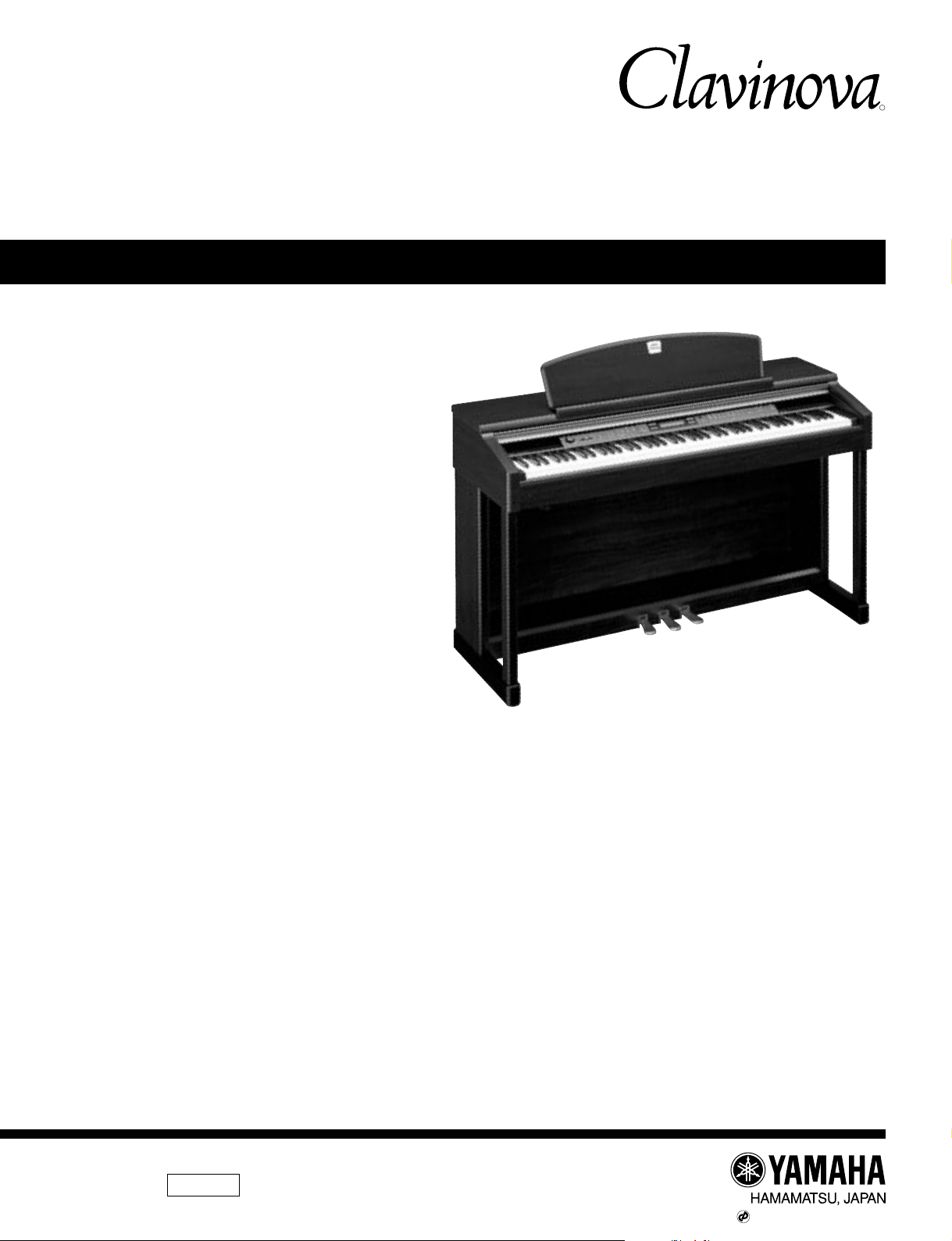
R
CLP-150/CLP-150M/
CLP-150C
SERVICE MANUAL
This document is printed on chlorine free (ECF) paper with soy ink.
CLP-150
■ CONTENTS
SPECIFICATIONS.............................................................................. 3
PANEL LAYOUT ................................................................................. 4
DISASSEMBLY PROCEDURE .......................................................... 6
LSI PIN DESCRIPTION ................................................................... 18
IC BLOCK DIAGRAM....................................................................... 23
CIRCUIT BOARDS .......................................................................... 24
TEST PROGRAM ............................................................................ 38
MIDI IMPLEMENTATION CHART .................................................... 42
PARTS LIST
OVERALL CIRCUIT DIAGRAM
BLOCK DIAGRAM
CIRCUIT BOARD LAYOUT
CL 001676
1.27K-9241 MI Printed in Japan ’02.06
CLP-150/CLP-150M/CLP-150C
IMPORTANT NOTICE
This manual has been provided for the use of authorized Yamaha Retailers and their service personnel. It has been assumed
that basic service procedures inherent to the industry, and more specifically Yamaha Products, are already known and
understood by the users, and have therefore not been restated.
WARNING : Failure to follow appropriate service and safety procedures when servicing this product may result in
personal injury, destruction of expensive components and failure of the product to perform as
specified. For these reasons, we advise all Yamaha product owners that all service required should
be performed by an authorized Yamaha Retailer or the appointed service representative.
IMPORTANT : This presentation or sale of this manual to any individual or firm does not constitute authorization,
certification, recognition of any applicable technical capabilities, or establish a principal-agent
relationship of any form.
The data provided is believ ed to be accurate and applicab le to the unit (s) indicated on the cov er. The research engineering,
and service departments of Yamaha are continually striving to improve Yamaha products. Modifications are, therefore,
inevitable and changes in specification are subject to change without notice or ob ligation to retrofit. Should any discrepancy
appear to exist, please contact the distributor’s Service Division.
WARNING : Static discharges can destroy expensive components. Discharge any static electricity your body
may have accumulated by grounding yourself to the ground bus in the unit (heavy gauge black wires
connect to this bus).
IMPORTANT : Turn the unit OFF dur ing disassembly and parts replacement. Recheck all work before you apply
power to the unit.
WARNING : CHEMICAL CONTENT NOTICE !
The solder used in the production of this product contains LEAD. In addition, other electrical/electronic and/or plastic
(where applicable) components may also contain traces of chemicals found by the California Health and Welfare Agency
(and possibly other entities) to cause cancer and/or birth defects or other reproductive harm.
DO NOT PLACE SOLDER, ELECTRICAL/ELECTRONIC OR PLASTIC COMPONENTS IN YOUR MOUTH FOR ANY
REASON WHAT SO EVER!
Avoid prolonged, unprotected contact betw een solder and your skin! When soldering, do not inhale solder fumes or expose
eyes to solder/flux vapor!
If you come in contact with solder or components located inside the enclosure of this product, wash your hands before
handling food.
IMPORTANT NOTICE FOR THE UNITED KINGDOM
Connecting the Plug and Cord
IMPORTANT . The wires in this main lead are coloured inaccordance with the following code:
BLUE: NEUTRAL
BROWN: LIVE
As the colours of the wires in the main lead of this apparatus may not correspond with the coloured markings identifying the
terminals in your plug, proceed as follows:
The BLUE wire must be connected to the terminal that is marked with the letter N (or coloured BLACK).
The BROWN wire must be connected to the terminal that is marked with the letter L (or coloured RED).
Be certain that neither core is connected to the earth terminal of the three pin plug.
■ WARNING
Components having special characteristics are marked Z and must be replaced with parts having specification equal to
those originally installed.
2
CLP-150/CLP-150M/CLP-150C
■ SPECIFICATIONS
Keyboard 88 keys (A-1–C7)
Sound Source AWM Dynamic Stereo Sampling
Polyphony max. 128 voices
Voice Selection Panel preset for manual performance: 38 voices,
XG voices: 480 voices + 12 drum kits
Effect
Reverb, Chorus, Brilliance, Variation effect, Insertion effect x 3
Controls Dual, Split
Display LCD
Recording/Playback 16-track recording/playback, tempo adjustment
Pedal Damper, Sostenuto, Soft
Demo Songs 16 voice demo songs, 50 preset songs
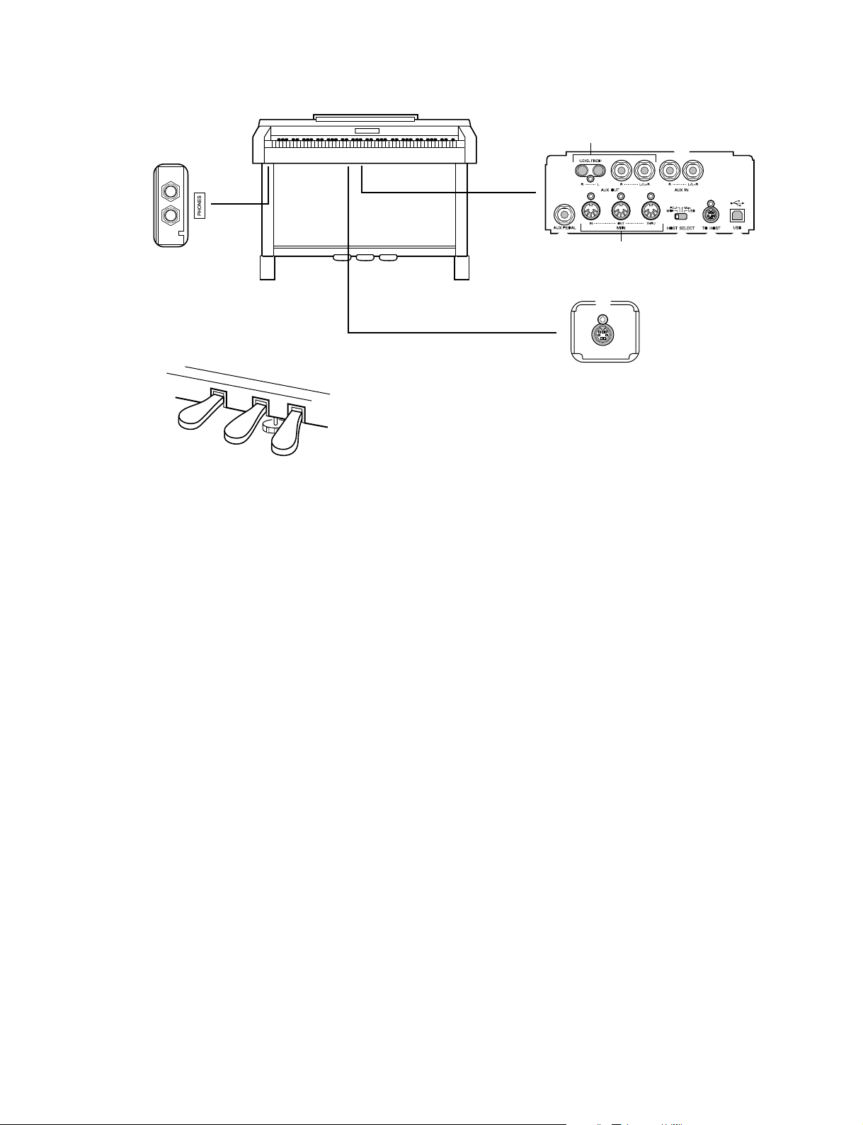
Jacks/Connectors
MIDI (IN/OUT/THRU), PHONES X2, AUX IN, AUX OUT(L/L+R,R),
AUX OUT (LEVEL FIXED)(L,R), TO HOST, USB, AUX PEDAL
Main Amplifiers 60W x 2
Speakers 16cm x 2, 5cm x 2
Output Impedance AUX OUT : about 600 Ω (594 Ω)
AUX OUT (Fix) : 680 Ω
PHONES : 33 Ω
Dimensions (W x D x H) 1381mm x 513mm x 853mm [54-3/8" x 20-3/16" x 33-9/16"]
(with music stand) (1381mm x 513mm x 1022mm [54-3/8" x 20-3/16" x 40-1/4"])
Weight 61.5 kg, 135lbs., 9oz
Attachment Keyboard Cover, Music Stand
Accessories Owner’s Manual, Reference Booklet,
“50 Greats for the Piano” Score Collection
3
CLP-150/CLP-150M/CLP-150C
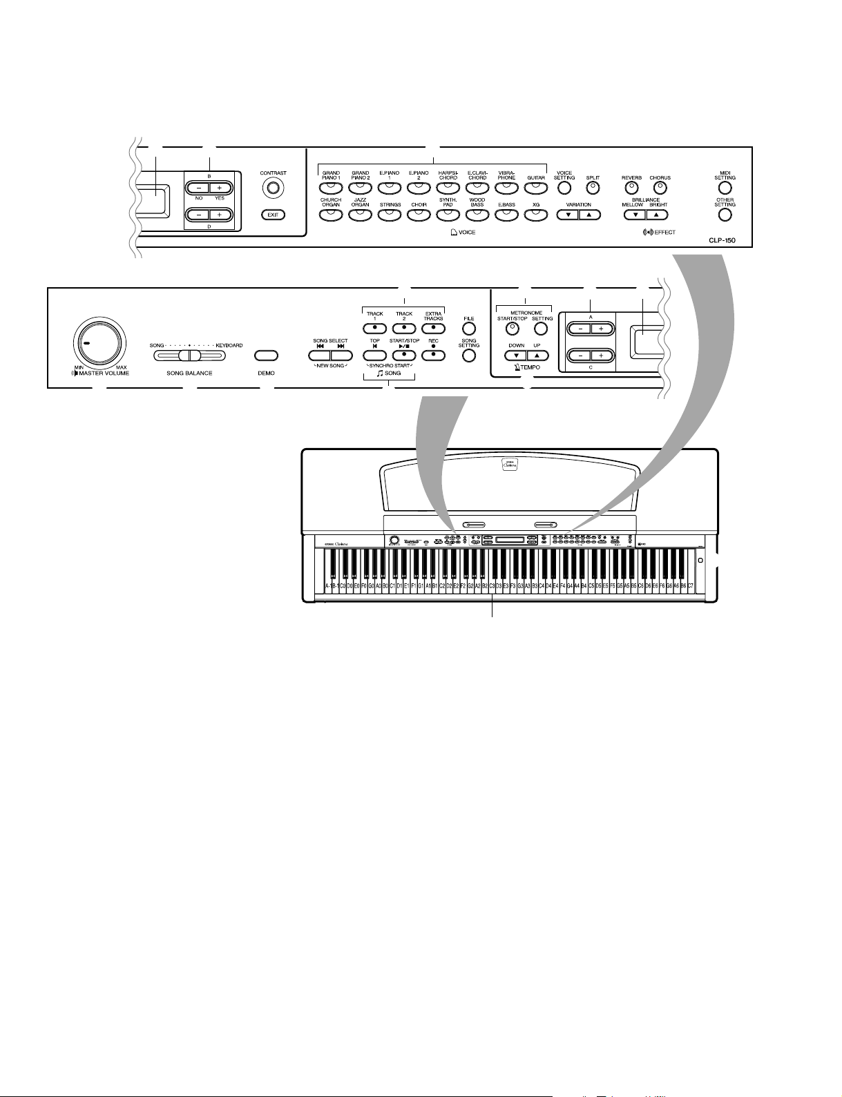
■ PANEL LAYOUT
!4
y
!7
!1
!8
@2
!9
!3
@0
@3
!4
@1
@4
@5
!3
!5
!6
u
o
ew
r
t
i
!0
!2
q [POWER] switch
w [MASTER VOLUME] knob
e [SONG BALANCE] knob
r [DEMO] button
t SONG SELECT [ T ] [ Y ] buttons
y [TRACK1] [TRACK2] [EXTRA TRACKS] buttons
u [FILE] button
i SONG [TOP]/[START/STOP] buttons
o [REC] button
!0 [SONG SETTING] button
!1 METRONOME [START/STOP]/[SETTING] buttons
!2 TEMPO [DOWN] [UP] buttons
!3 LCD buttons
A [ – ] [ + ]/B [ – (NO)] [ + (YES)]/C [ – ] [ + ]/D [ – ] [ + ]
!4 LCD screen
q
Center “C”
!5 [CONTRAST] knob
!6 [EXIT] button
!7 Voice group buttons
!8 [VOICE SETTING] button
!9 [SPLIT] button
@0 [REVERB] button
@1 [CHORUS] button
@2 VARIA TION [ G ] [ H ] buttons
@3 BRILLIANCE [MELLOW] [BRIGHT] buttons
@4 [MIDI SETTING] button
@5 [OTHER SETTING] button
4
CLP-150/CLP-150M/CLP-150C
@7
@6
@8
@9
#1
#7
#0
PEDAL
#2
#6
#3
#4
#5
@6 [PHONES] jacks
@7 Soft pedal
@8 Sostenuto pedal
@9 Damper pedal
#0 [PEDAL] connector
#1 [AUX PEDAL] jack
#2 MIDI [IN] [OUT] [THRU] connectors
#3 [HOST SELECT] switch
#4 [TO HOST] connector
#5 [USB] connector
#6 AUX IN [L/L+R] [R] jacks
#7 AUX OUT [L/L+R] [R]/ (LEVEL FIXED) [L] [R] jacks
5
CLP-150/CLP-150M/CLP-150C
■ DISASSEMBLE PROCEDURE
1. Music Rest Assembly
(Time required : About 3 minutes)
Remove the four (4) screws marked [51]. The music rest
assembly can then be removed. (Fig. 1)
Music rest assembly
[51]
[51]: Bind Head Tapping Screw-1 3.0x16 MFZN2BL (EP030310)
(Fig. 1)
2. Top Board Assembly
(Time required : About 3 minutes)
2-1 Remove the three (3) screws marked [57].
2-2 Move the top board assembly forward, lift it. (Fig. 2)
3. Back Board Assembly
(Time required : About 3 minutes)
Remove the two (2) screws mark ed [B] and the four (4)
screws marked [D]. The back board assembly can then
be removed. (Fig. 3)
[B]
[D][D]
Back board assembly
CLP-150/150M
[B]: Truss Head Screw 4.0x12 MFZN2BL (VP367300)
[D]: Truss Head Tapping Screw-1 4.0x20 MFZN2BL (03747290)
CLP-150C
[B]: Truss Head Screw 4.0x12 MFC2 (V6135000)
[D]: Truss Head Tapping Screw-1 4.0x20 MFC2 (VB164600)
Top board assembly
[57]
CLP-150/150M
[57]: Truss Head Screw 4.0x20 MFZN2BL (VB934000)
CLP-150C
[57]: Truss Head Screw 4.0x20 MFC2 (V6141100)
(Fig. 2)
(Fig. 3)
AC cord
PK-LF cable
(Fig. 3-1)
6
CLP-150/CLP-150M/CLP-150C
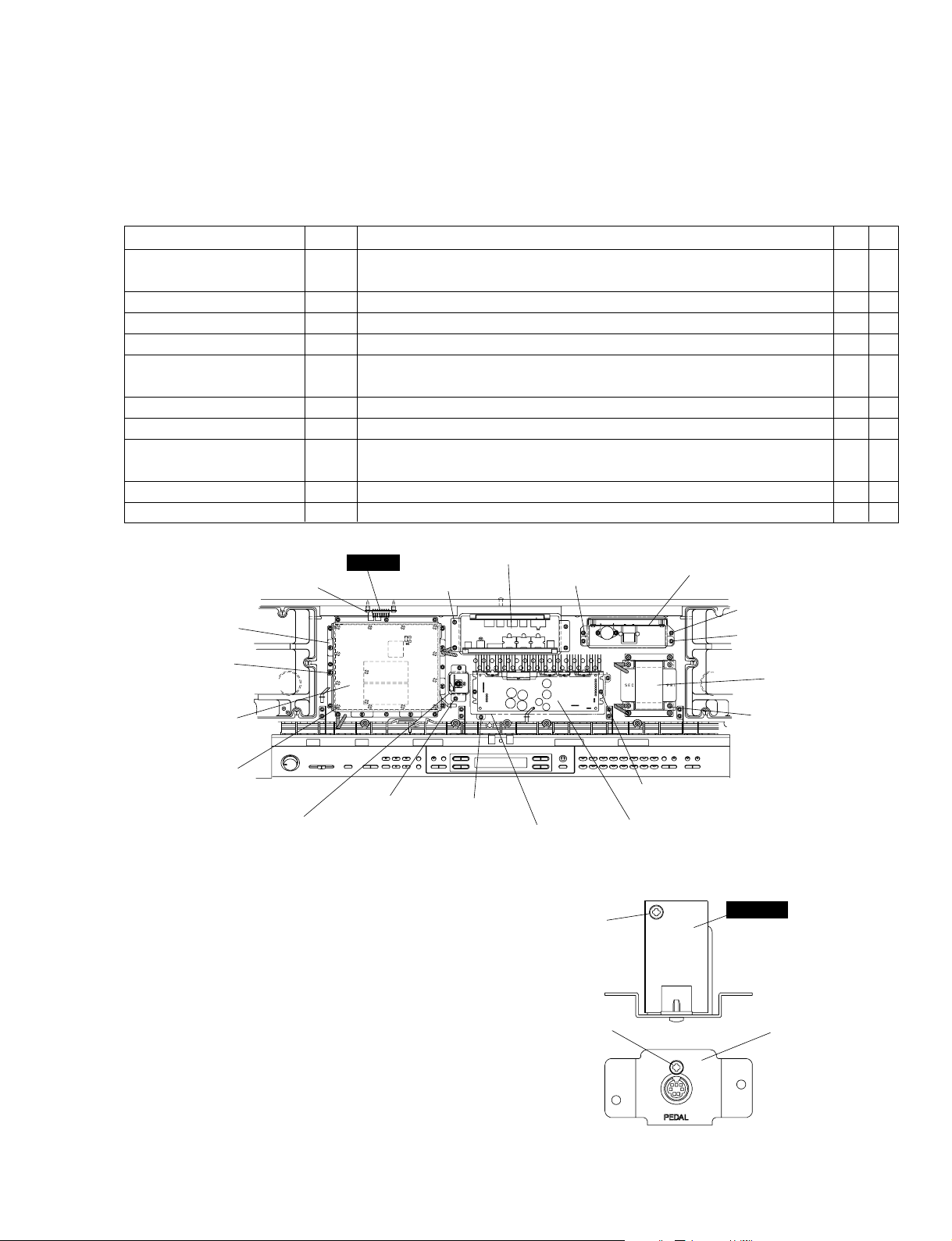
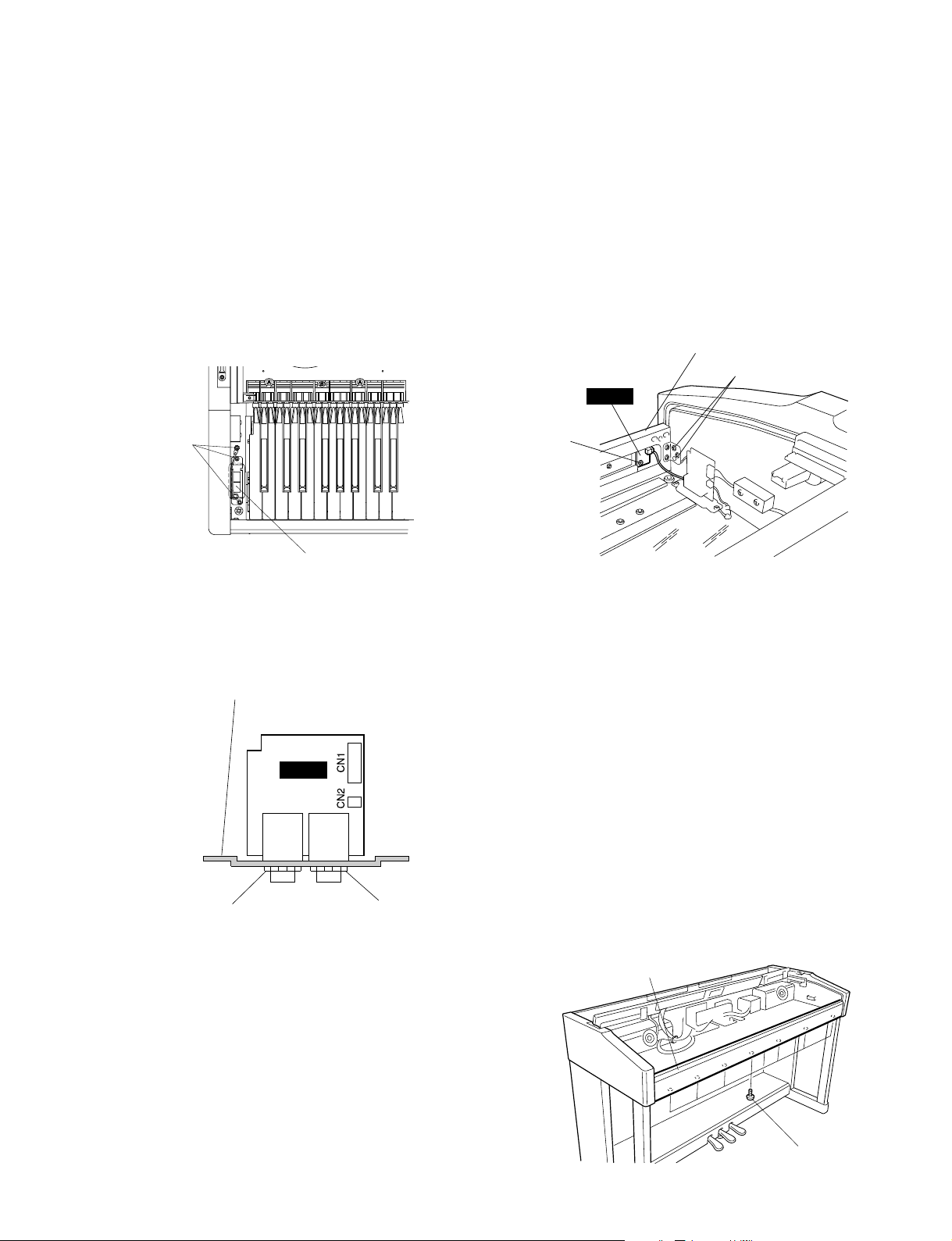
4. Circuit Boards & Assemblies Inside of Main Unit
(Time required : About 10 minutes each)
4-1 Remove the top board assembly. (See procedure 2)
4-2 Each circuit board and assembly can be removed by
removing its fixing screws as listed below.
Circuit board and Assembly Ref. No. Screw QTY Fig.
DM Shield Cover Assembly 56A Bind Head Tapping Screw-B 3.0x6 MFZN2Y (EP600130) 6 4
(U.S.A. model only)
DM Assembly 56B Bind Head Tapping Screw-B 3.0x6 MFZN2Y (EP600130) 12 4
Network Circuit Board 58 Bind Head Tapping Screw-1 3.5x20 MFZN2Y (EP030470) 4 4
PK Connector Assembly 81A Bind Head Tapping Screw-1 3.5x12 MFZN2Y (EP030240) 2 4
MA Cover Assembly 81B Bind Head Tapping Screw-1 3.5x12 MFZN2Y (EP030240) 2 4
(U.S.A. model only)
MA120 Assembly 81C Bind Head Tapping Screw-1 3.5x12 MFZN2Y (EP030240) 2 4
Jack Assembly 81D Bind Head Tapping Screw-1 3.5x12 MFZN2Y (EP030240) 4 4
FU Cover Assembly 81E Bind Head Tapping Screw-1 3.5x12 MFZN2Y (EP030240) 2 4
(U.S.A. model only)
FU120LB Assembly 81F Bind Head Tapping Screw-1 3.5x12 MFZN2Y (EP030240) 2 4
Power Transformer 80A Bind Head Tapping Screw-B 4.0x10 MFZN2BL (EP600240) 4 4
NET1
[58] x 4
DM shield cover
assembly
[56A] x 6
DM assembly
[56B] x 12
[81A] x 2
PK connector assembly
[81D] x 4
[81B] x 2
5. PEDAL (DJK) Circuit Board
(Time required : About 10 minutes)
5-1 Remove the top board assembly. (See procedure 2)
5-2 Disconnect the PK-LF cable. (Fig. 3)
5-3 Remove the PK connector assembly. (See procedure 4)
5-4 Remove the two (2) screws marked [26c]. The pedal
connector angle can then be removed from the PEDAL
(DJK) circuit board. (Fig. 5)
Jack assembly
FU cover assembly
MA cover assembly
(Fig. 4)
[26c]
[26c]
FU120LB assembly
[81F] x 2
[81E] x 2
Power transformer
[80A] x 4
[81C] x 2
MA120 assembly
PEDAL
(DJK)
Pedal connector angle
[26c]: Bind Head Tapping Screw-B 3.0x8 MFZN2BL (EP600190)
(Fig. 5)
7
CLP-150/CLP-150M/CLP-150C
6. MA120 Circuit Board
(Time required : About 15 minutes)
6-1 Remove the top board assembly. (See procedure 2)
6-2 Remove the MA120 assembly. (See procedure 4)
6-3 Remove the five (5) screws marked [1A], the four (4)
screws marked [2] and the screw marked [3A]. The
MA120 circuit board can then be removed. (Fig. 6)
[2]
[1A]: Bind Head Tapping Screw-B 4.0x8 MFZN2Y (EP640410)
[2]: Bind Head Tapping Screw-B 3.0x10 MFZN2Y (EP600220)
[3A]: Bind Head Tapping Screw-B 3.0x16 MFZN2Y (EP600390)
[1A]
[3A]
[1A]
(Fig. 6)
[2] [2] [2]
MA120
[1A]
8. FU120L Circuit Board
(Time required : About 15 minutes)
8-1 Remove the top board assembly. (See procedure 2)
8-2 Disconnect the AC cord.
8-3 Remove the FU120LB assembly. (See procedure 4)
8-4 Remove the four (4) screws marked [1B]. The FU120L
circuit board can then be removed. (Fig. 8)
8-5 Remove the two (2) screws marked [4C]. (Fig. 8)
(General export model only)
[1B]
FU120L
[4C]
[1B]: Bind Head Tapping Screw-B 3.0x8 MFZN2BL (EP600190)
[4C]: Bind Head Screw 3.0x10 MFZN2BL (EG330380)
[1B]
7. DJK Circuit Board, AJK Circuit Board
(Time required : About 15 minutes)
7-1 Remove the top board assembly. (See procedure 2)
7-2 Remove the jack assembly. (See procedure 4)
7-3 Remove the six (6) screws marked [4A] and the
hexagonal nut marked [6A]. The DJK circuit board can
then be removed. (Fig. 7)
7-4 Remove the five (5) screws marked [4B] and the four
(4) hexagonal nuts marked [6B]. The AJK circuit board
can then be removed. (Fig. 7)
[4B]
DJK
[4A]
[4B]
[4B]
AJK
[4A]
[6B]
(Fig. 8)
[6A]
[4]: Bind Head Tapping Screw-B 3.0x8 MFZN2BL (EP600190)
[6]: Hexagonal Nut 12.0 14x2 MFZN2BL (VB508600)
8
[4A]
(Fig. 7)
CLP-150/CLP-150M/CLP-150C
[53]
[53]
[53]
[61B]
9. Key Cover Assembly
(Time required : About 10 minutes)
9-1 Close the key cover.
9-2 Remove the top board assembly. (See procedure 2)
9-3 Remove the screw mark ed [61A]. The rack cover L can
then be removed. (Fig. 9)
* The rack cover R can then be removed in the same
manner.
9-4 Set the left end of the rod at the slits of the guide and
then lift the rear key cover assembly. (Fig. 9-1)
9-5 Lean slightly the key cover assembly so that the guide
pin can be removed from the guide rail. (Fig. 9-2)
* When removing, be sure not to make scratches on the
side cover.
* When reinstalling the key cover assembly, apply a
masking shield tape around the guide rail to prevent from
making scratches on the assembly.
Rack cover L
[61A]
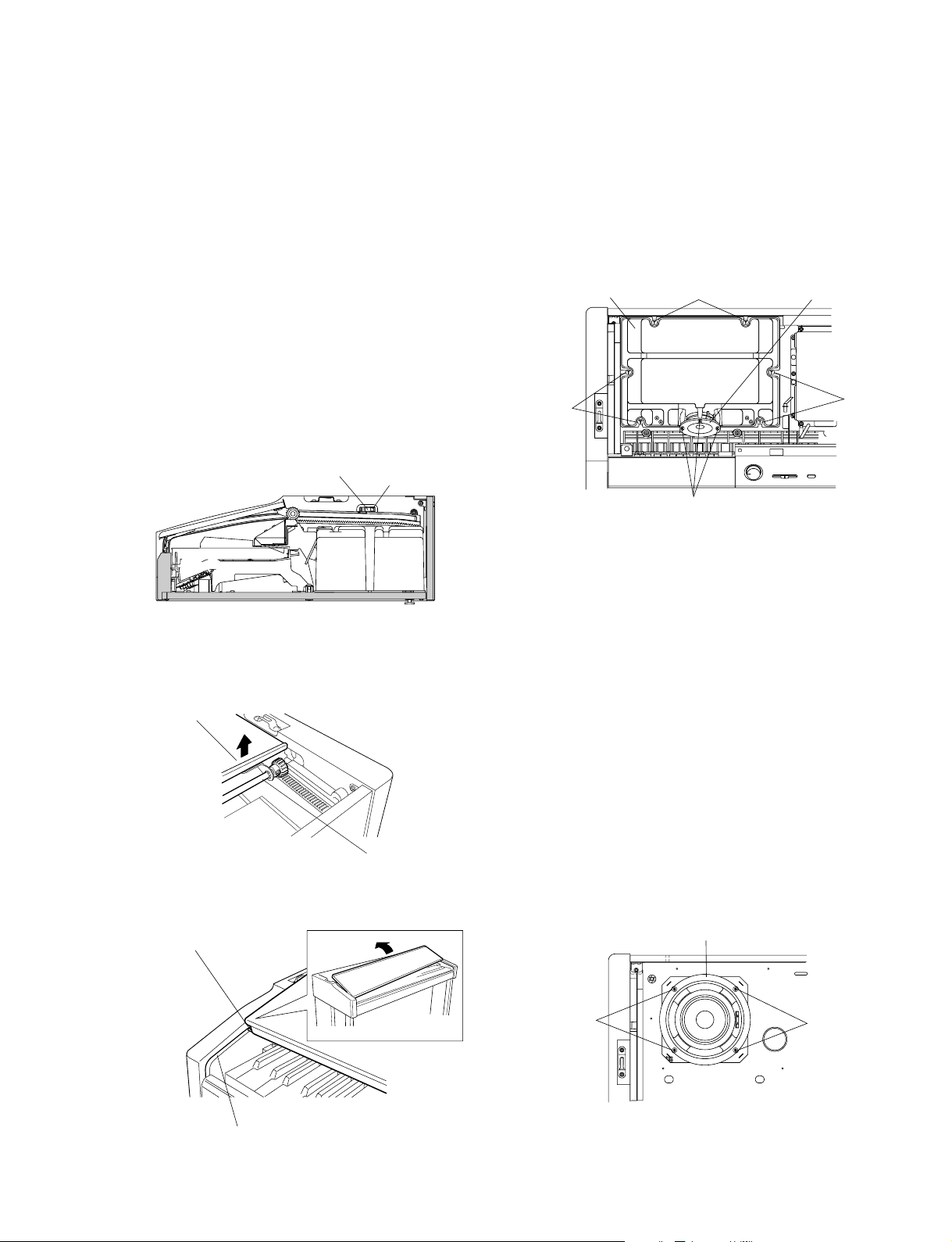
10. Speaker (Tweeter)
(Time required : About 10 minutes)
10-1 Remove the top board assembly. (See procedure 2)
10-2 Remove the key cover assembly. (See procedure 9)
10-3 Remove the three (3) screws marked [61B]. The speaker
(tweeter) can then be removed. (Fig. 10)
* The left and right speaker (tweeter) each can then be
removed in the same manner.
Speaker box assembly
[61B]: Bind Head Tapping Screw-B 3.0x8 MFZN2Y (EP600250)
[53]: Truss Head Tapping Screw-1 3.5x14 MFZN2Y (EN630230)
(Fig. 10)
Speaker (tweeter)
[61A]: Bind Head Tapping Screw-B 3.0x8 MFZN2Y (EP600250)
(Fig. 9)
Key cover assembly
Rod
(Fig. 9-1)
Guide pin
11. Speaker Box Assembly , Speaker (W oof er)
(Time required : About 15 minutes)
11-1 Remove the top board assembly. (See procedure 2)
11-2 Remove the key cover assembly. (See procedure 9)
11-3 Remove the speaker (tweeter). (See procedure 10)
11-4 Remove the six (6) screws marked [53]. The speaker
box assembly can then be removed. (Fig. 10)
* The left and right speaker box assembly each can then
be removed in the same manner.
* The phillips type screwdriver used here must be 15cm
or longer.
11-5 Remove the four (4) screws marked [68]. The speaker
(woofer) can then be removed. (Fig. 11)
Speaker (woofer)
[68]
[68]
Guide rail
(Fig. 9-2)
[68]: Truss Head Tapping Screw-1 4.0x20 MFZN2Y (20338800)
(Fig. 11)
9
CLP-150/CLP-150M/CLP-150C
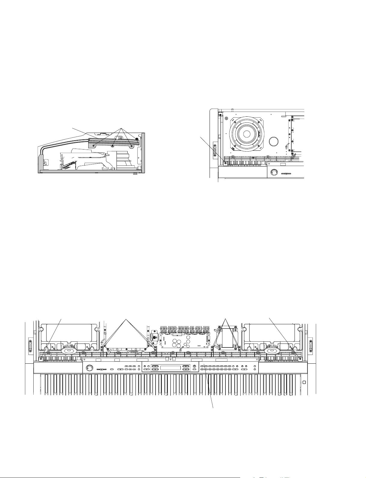
12. Rack Assembly
(Time required : About 15 minutes)
12-1 Remove the top board assembly. (See procedure 2)
12-2 Remove the key cover assembly. (See procedure 9)
12-3 Remove the speaker box assembly. (See procedure 11)
12-4 Remove the four (4) screws marked [6C] and the screw
marked [80B]. The rack assembly can then be removed.
(Fig. 12-1, Fig. 12-2)
* The left and right rack assembly each can then be
removed in the same manner.
Rack assembly
[6C]: Bind Head Tapping Screw-1 3.5x16 MFZN2BL (EP030260)
(Fig. 12-1)
[6C]
13. Panel Assembly
(Time required : About 20 minutes)
13-1 Remove the top board assembly. (See procedure 2)
13-2 Remove the key cover assembly. (See procedure 9)
13-3 Remove the screw marked [80B], the screw marked
[80C] and the eight (8) screws marked [81G]. The panel
assembly can then be removed. (Fig. 13)
[80B]
[80B]: Bind Head Tapping Screw-B 4.0x10 MFZN2BL (EP600240)
(Fig. 12-2)
10
[80B]
[81G]
[80]: Bind Head Tapping Screw-B 4.0x10 MFZN2BL (EP600240)
[81G]:Bind Head Tapping Screw-1 3.5x12 MFZN2Y (EP030240)
(Fig. 13)
[81G]
Panel assembly
[80C]
CLP-150/CLP-150M/CLP-150C
PNL
PNL
PNR
PNR
MV2
[34C] x 3
[34A] x14
[35] x 3
[34B] x 17
[34B]
[34A]
[34A]
MV2
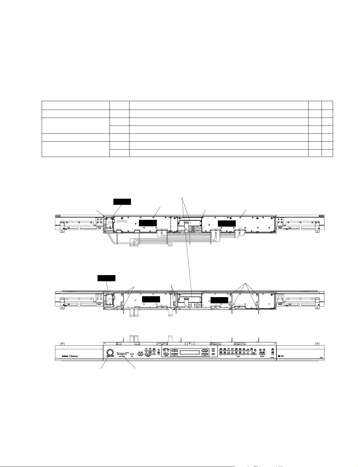
14.
Circuit Boards & Assemblies of Panel Assembly
(Time required : About 25 minutes)
14-1 Remove the top board assembly. (See procedure 2)
14-2 Remove the key cover assembly. (See procedure 9)
14-3 Remove the panel assembly. (See procedure 13)
14-4 Ea ch c ir cuit board and assembly can be removed by
removing its fixing screws as listed below.
Circuit board and Assembly Ref. No. Screw QTY Fig.
LCD Assembly 35 Bind Head Tapping Screw-B 2.6x10 MFZN2Y (VD791000) 3 14
PNL Circuit Board Slide knob 114
34A Bind Head Tapping Screw-B 3.0x8 MFZN2Y (EP600250) 18 14
PNR Circuit Board 34B Bind Head Tapping Screw-B 3.0x8 MFZN2Y (EP600250) 21 14
MV2 Circuit Board Knob 114
34C Bind Head Tapping Screw-B 3.0x8 MFZN2Y (EP600250) 3 14
LCD assembly
Knob
Slide knob
(Fig. 14)
11
CLP-150/CLP-150M/CLP-150C
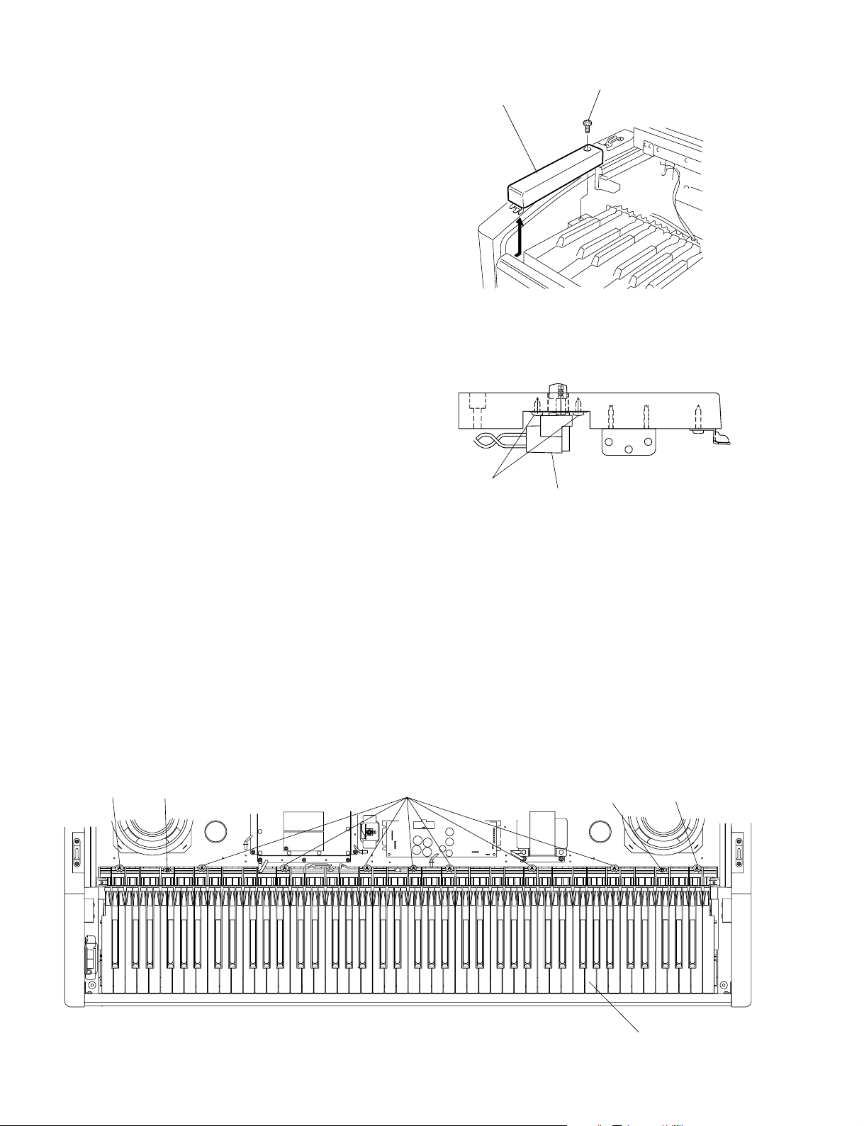
15. End Block Assembly
(Time required : About 25 minutes)
15-1 Remove the top board assembly. (See procedure 2)
15-2 Remove the key cover assembly. (See procedure 9)
15-3 Remove the panel assembly. (See procedure 13)
15-4 Remove the screw marked [69]. The end block assembly
L can then be removed. (Fig. 15)
* The end block assembly R can then be removed in the
same manner.
16. Power Switch Assembly
(Time required : About 25 minutes)
16-1 Remove the top board assembly. (See procedure 2)
16-2 Remove the key cover assembly. (See procedure 9)
16-3 Remove the panel assembly. (See procedure 13)
16-4 Remove the end block assembly R. (See procedure 15)
16-5 Remove the two (2) screws marked [8]. The po wer switch
assembly can then be removed. (Fig. 16)
End block assembly L
[69]: Truss Head Tapping Screw-1 3.5x30 MFZN2Y (VA076400)
[8]
Power switch assembly
[69]
(Fig. 15)
17. Keyboard Assembly
(Time required : About 30 minutes)
17-1 Remove the top board assembly. (See procedure 2)
17-2 Remove the key cover assembly. (See procedure 9)
17-3 Remove the speaker box assembly. (See procedure 11)
17-4 Remove the rack assembly. (See procedure 12)
17-5 Remove the panel assembly. (See procedure 13)
17-6 Remove the end block assembly L and R.
(See procedure 15)
17-7 Remove the two (2) screws marked [54] and the nine
(9) screws marked [52]. The ke yboard assembly can then
be removed. (Fig. 17)
[52]
[54]
[8]: Bind Head Tapping Screw-1 3.5x10 MFZN2BL (EP030320)
(Fig. 16)
[52]
[54]
[52]
12
[54]: Bind Head Tapping Screw-1 4.0x14 MFZN2Y (EP040230)
[52]: Pan Head Screw PW5.0x25 MFZN2Y (VV040700)
(Fig. 17)
Keyboard assembly
CLP-150/CLP-150M/CLP-150C
18. Headphones Jack Assembly, HP Circuit Board
18-1 Remove the top board assembly. (See procedure 2)
18-2 Remove the key cover assembly. (See procedure 9)
18-3 Remove the panel assembly. (See procedure 13)
18-4 Remove the end block assembly L. (See procedure 15)
18-5 Remove the three (3) screws marked [81H]. The
headphones jack assembly can then be removed.
(Fig. 18)
18-6 Remove the two (2) hexagonal nuts marked [3B]. The
headphone angle can then be removed from the HP
circuit board. (Fig. 18-1)
[81H]
(Time required : About 30 minutes)
19. PL Circuit Board
(Time required : About 30 minutes)
19-1 Remove the top board assembly. (See procedure 2)
19-2 Remove the key cover assembly. (See procedure 9)
19-3 Remove the speaker box assembly. (See procedure 11)
19-4 Remove the rack assembly. (See procedure 12)
19-5 Remove the panel assembly. (See procedure 13)
19-6 Remove the end block assembly L and R.
(See procedure 15)
19-7 Remove the keyboard assembly. (See procedure 17)
19-8 Remove the screw marked [6C]. The PL circuit board
can then be removed. (Fig. 19)
Front rail assembly
[60A]
PL
[6C]
Headphones jack assembly
[81H]:Bind Head Tapping Screw-1 3.5x12 MFZN2Y (EP030240)
(Fig. 18)
Headphone angle
HP
[3B]
[3B]: Hexagonal Nut 12.0 14x2 MFZN2BL (VB508600)
(Fig. 18-1)
[3B]
[6C]: Bind Head Tapping Screw-1 3.5x12 MFZN2BL (EP030340)
[60A]: Bind Head Tapping Screw-1 3.5x16 MFZN2Y (EP030190)
(Fig. 19)
20. Front Rail Assembly
(Time required : About 40 minutes)
20-1 Remove the top board assembly. (See procedure 2)
20-2 Remove the key cover assembly. (See procedure 9)
21-3 Remove the speaker box assembly. (See procedure 11)
21-4 Remove the rack assembly. (See procedure 12)
20-5 Remove the panel assembly. (See procedure 13)
20-6 Remove the end block assembly L and R.
(See procedure 15)
20-7 Remove the keyboard assembly. (See procedure 17)
20-8 Remove the two (2) screws marked [60A] from both
sides of the assembly. (Fig. 19)
20-9 Remove the seven (7) screws marked [55A]. The front
rail assembly can then be removed. (Fig. 20)
Front rail assembly
[55A]
[55A]: Truss Head Tapping Screw-1 3.5x30 MFZN2BL (VU952600)
(Fig. 20)
13
CLP-150/CLP-150M/CLP-150C
21. Back Top Board Assembly
(Time required : About 40 minutes)
21-1 Remove the top board assembly. (See procedure 2)
21-2 Remove the key cover assembly. (See procedure 9)
21-3 Remove the speaker box assembly L and R.
(See procedure 11)
21-4 Remove the three (3) screws marked [60B] and the screw
marked [81I] from both sides of the assembly.
(Fig. 21-1)
21-5 Remove the four (4) screws marked [55B]. The back
top board assembly can then be removed. (Fig. 21-2)
Back top board assembly
[60B]
[81I]
[60B]: Bind Head Tapping Screw-1 3.5x16 MFZN2Y (EP030190)
[81I]: Bind Head Tapping Screw-1 3.5x12 MFZN2Y (EP030240)
(Fig. 21-1)
Back top board assembly
Main Unit
[A]
[A]
[A]: Bind Head Screw 6.0x16 MFZN2BL (EG360020)
(Fig. 22)
23. Arm Assembly
(Time required : About 40 minutes)
23-1 Remove the top board assembly. (See procedure 2)
23-2 Remove the key cover assembly. (See procedure 9)
23-3 Remove the speaker box assembly L and R.
(See procedure 11)
23-4 Remove the rack assembly. (See procedure 12)
23-5 Remove the panel assembly. (See procedure 13)
23-6 Remove the end block assembly L and R.
(See procedure 15)
23-7 Remove the keyboard assembly. (See procedure 17)
23-8 Remove the main unit. (See procedure 22)
23-9 Remove the two (2) screws marked [60A]. (Fig. 19)
23-10 Remove the three (3) screws marked [60B]. (Fig. 21-1)
23-11 Remove the five (5) screws marked [55C]. The arm
assembly can then be removed. (Fig. 23)
* The left and right arm assembly each can then be
removed in the same manner.
[55B]
[55B]: Truss Head Tapping Screw-1 3.5x30 MFZN2BL (VU952600)
(Fig. 21-2)
22. Main Unit (Time required : About 15 minutes)
22-1 Disconnect the AC cord and the PK-LF cable.
22-2 Spread a soft cloth like a blanket on the floor where the
main unit is to be placed in advance.
22-3 Remove the six (6) screws marked [A]. (Fig. 22)
22-4 Move the main unit rearward, lift it and place it on the
cloth gently.
* For safety, this work should be done by two persons.
* When removing the main unit from the stand, use care
not to have your finger caught.
14
[55C]
Arm assembly L
[55C]:Truss Head Tapping Screw-1 3.5x30 MFZN2BL (VU952600)
(Fig. 23)
CLP-150/CLP-150M/CLP-150C
24. Side Board Assembly
(Time required : About 15 minutes)
24-1 Remove the back board assembly. (See procedure 3)
24-2 Remove the main unit. (See procedure 22)
24-3 Remove the two (2) screws marked [CA]. The side board
unit can then be removed. (Fig. 24)
* The left and right side board unit each can then be
removed in the same manner.
Side board unit R
Side board unit L
25. Pedal Box Assembly, Pedal Assembly
(Time required : About 15 minutes)
25-1 Disconnect the PK-LF cable.
25-2 With a soft cloth like a blanket placed on the floor, place
the main unit on its back board gently. (Fig. 25)
* For safety, this work should be done by two persons.
25-3 Remove the four (4) screws marked [CB]. The pedal
box assembly can then be removed. (Fig. 25)
25-4 Remove the eight (8) screws marked [6D] and the screw
marked [7]. The pedal assembly can then be removed.
(Fig. 25-1)
Pedal box assembly
[CA]
[CA]: Truss Head Screw 6.0x25 MFZN2BL (VQ448400)
(Fig. 24)
[7]
[6D]
[CB]
[CB]: Truss Head Screw 6.0x25 MFZN2BL (VQ448400)
(Fig. 25)
[6D]
Pedal assembly
[6D]
[6D]: Bind Head Tapping Screw-1 4.0x14 MFZN2Y (EP040230)
[7]: Truss Head Tapping Screw-1 3.5x20 MFZN2Y (EN630260)
(Fig. 25-1)
15

CLP-150/CLP-150M/CLP-150C
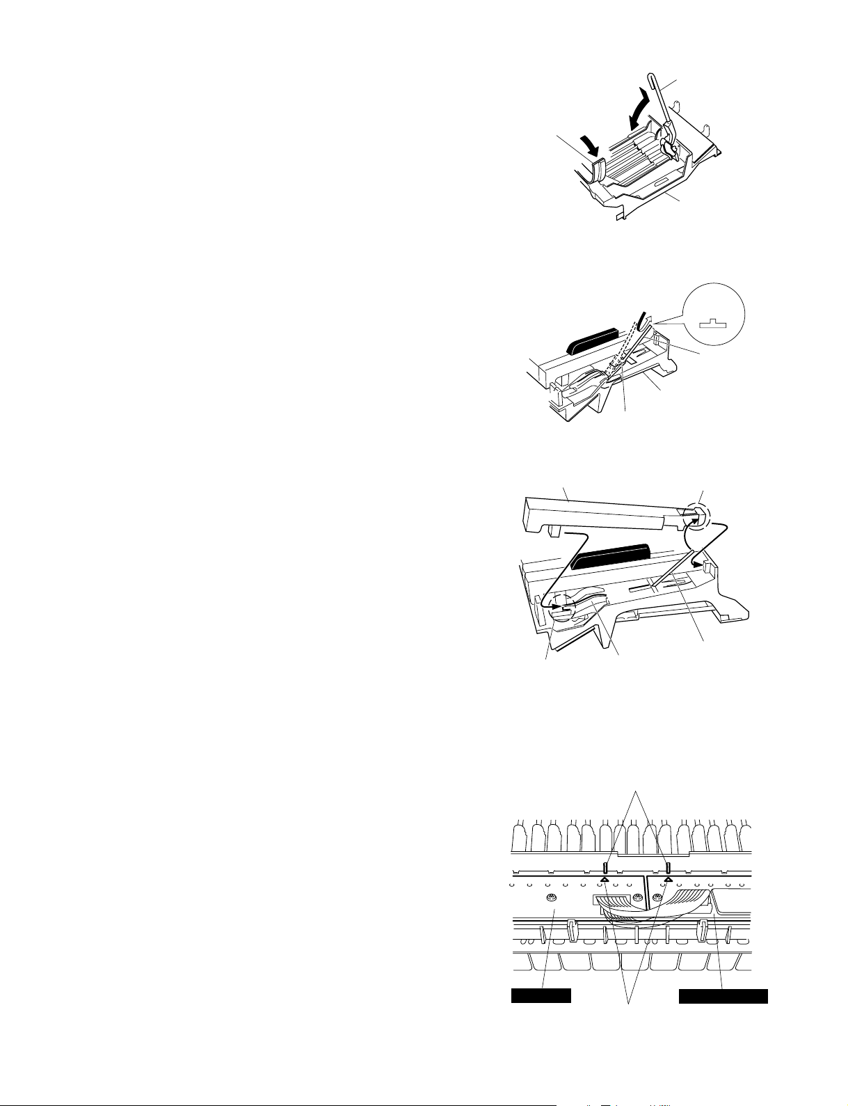
26. Disassembling the Keyboard
(Time required : About 15 minutes)
*
After inserting a round stick (Rod: TX000670) between the
frame and the keys, remove the circuit boards. (Fig. 26)
26-1 GHD EBUS L Circuit Board
Remove the sev en (7) scre ws marked [260A]. The GHD
EBUS L circuit board can then be removed. (Fig. 26)
26-2 GHD M Circuit Board
Remove the fi ve (5) screws mark ed [260B] and the screw
marked [262]. The GHD M circuit board can then be
removed. (Fig. 27)
33-3 GHD H Circuit Board
Remove the four (4) screws marked [260C] and the scre w
marked [262]. The GHD H circuit board can then be
removed. (Fig. 27)
*
Keys can be removed without remo ving the circuit boar ds.
* After removing the GHD EBUS L, GHD M and GHD H
circuit boards, and the rubbers can then be removed.
26-4 White key
Insert a thin plate between the white keys, near the
triangle mark around the fulcrum of the key, and press
down the stopper marked [A] to remove the key.
(Fig. 28, Fig. 29)
* Take care not to damage the key spring when removing
a key.
* A black key can be removed after the white keys on either
side have been removed.
26-5 Hammer, White Key
After a key has been removed, push a key spring down
once to take it out of the hook. (Fig. 30)
Place the keyboard assembly upside-down and peel the
stopper away. The hammer of the white key can then be
removed. (Fig. 31)
* The hammer of the black key can then be removed in
the same manner.
White key
Round stick
(Rod: TX000670)
(Fig. 26)
GHD EBUS LGHD MGHD H
[260C] [260B] [260A][262]
[260]: Bind Head Tapping Screw-P 3.0x10 MFZN2 (VT413400)
[262]: PW Head Tapping Screw-P 3.0x10⁻¹⁰ MFC2BL (V8833200)
(Fig. 27)
Thin metal plate etc
[A]
(Fig. 29)
Spring
(Fig. 30)
Spring
Round stick
(Rod: TX000670)
Hook
Hammer, white key
16
(Fig. 28)
Stopper (L88_W)
Triangle mark
(Fig. 31)
CLP-150/CLP-150M/CLP-150C
27. Assembling the Keyboard
(Time required : About 15 minutes)
27-1 Hammer, White Key (Hammer, Black Key)
Place the keyboard assembly upside-down, insert a
hammer assembly into the frame, and put the stopper
(L88_W) on. (Fig. 32)
* There are four (4) kinds of hammers that differ in weight.
27-2 Spring
Place the keyboard assembly rightside up. Fix key
springs on the frame by setting one at each slit and
pushing down once on each key spring. (Fig. 33)
* Be careful of the direction of the spring.
27-3 White Key (Black Key)
After a key has been fit to part [C] and key guide, make
sure that the spring is fixed to the key and then press
down part [B] of the key. (Fig. 34)
27-4 GHD EBUS L Circuit Board
Tighten the seven (7) screws marked [260A] to fix
the GHD EBUS L circuit board. (Fig. 27)
Stopper (L88_W)
White key
Hammer, white key
Frame
(Fig. 32)
Up
Spring
Frame
Hook
(Fig. 33)
[B]
34-5 GHD M Circuit Board
Tighten the five (5) screws marked [260B] and the
screw marked [262] to fix the GHD M circuit board.
(Fig. 27)
34-6 GHD H Circuit Board
Tighten the four (4) screws marked [260C] and the
screw marked [262] to fix the GHD H circuit board.
(Fig. 27)
* Install the circuit boards in the keyboard assembly so
that the hooks hold it as shown in figure 35.
[C]
Key guide
Spring
(Fig. 34)
Hooks
GHD M
GHD EBUS L
Triangle mark
(Fig. 35)
17
CLP-150/CLP-150M/CLP-150C
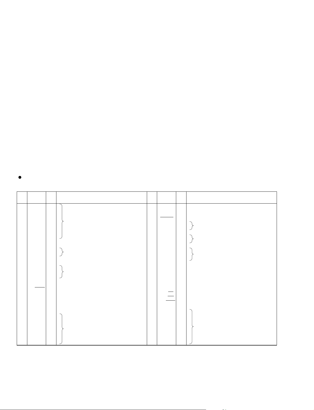
■ LSI PIN DESCRIPTION
HD6417709SHF200 (X2687A00) CPU (SH3) . . . . . . . . . . . . . . . . . . . . . . . . . . . . . . . . . . . . . . . . . . . 19
M66291GP (X2156A00) USB Controller . . . . . . . . . . . . . . . . . . . . . . . . . . . . . . . . . . . . . . . . . . . . . . 22
PCM1730E-1/2K (X2077A00) DAC (Digital to Analog Converter) . . . . . . . . . . . . . . . . . . . . . . . . . . . 22
T8F02TB-0102 (X0060A00) SWP50 (Tone Generator) . . . . . . . . . . . . . . . . . . . . . . . . . . . . . . . . . . . 20
µPD780031AYGK-N01-9ET (XZ916100) LED DRIVER/SWITCH SCAN E-PNS2a . . . . . . . . . . . . . 18
µPD780031AYGK-N02 (X0031100) LKS . . . . . . . . . . . . . . . . . . . . . . . . . . . . . . . . . . . . . . . . . . . . . . 18
µPD780031AYGK-N01-9ET (XZ916100) LED DRIVER/SWITCH SCAN E-PNS2a
µPD780031AYGK-N02 (X0031100) LKS
PIN
NO.
1
2
3
4
5
6
7
8
9
10
11
12
13
14
15
16
17
18
19
20
21
22
23
24
25
26
27
28
29
30
31
32
P50/A8
P51/A9
P51/A10
P53/A11
P54/A12
P55/A13
P56/A14
P57/A15
Vss0
DD
0
V
P30
P31
P32/SDA0
P33/SCL0
P34
P35
P36
P20/SI30
P21/SO30
P22/SCK30
P23RxD0
P24/TxD0
P25/ASCK0
VDD1
AVss
P17/ANI7
P16/ANI6
P15/ANI5
P14/ANI4
P13/ANI3
P12/ANI2
P11/ANI1
I/O FUNCTIONNAME
I/O
I/O
I/O
I/O
I/O
I/O
I/O
I/O
I/O
I/O
I/O
I/O
I/O
I/O
I/O
I/O
I/O
I/O
I/O
I/O
I/O
Port 5 / Higher address bus
-
-
-
I
I
I
I
I
I
I
Ground
Power supply
Port 3
Port 3 / Serial data input/output
Port 3 / Serial clock input/output
Port 3
Port 2 / Serial data input
Port 2 / Serial data output
Port 2 / Serial clock input/output
Port 2 / Serial data input
Port 2 / Serial data output
Port 2 / Serial clock input/output
Power supply
Ground
Port 1 / A/D converter analog input
PIN
NO.
33
P10/ANI0
34
AV
35
AV
36
RESET
37
XT2
38
XT1
39
40
41
42
Vss1
43
P00/INTP0
44
P01/INTP1
45
P02/INTP2
46
P03/INTP3/ADTRG
47
P70/TI00/TO0
48
P71/TI01
P72/TI50/TO50
49
50
P73/TI51/TO51
P74/PCL
51
P75/BUZ
52
P64/RD
53
P65/WR
54
P66/WAIT
55
P67/ASTB
56
P40/AD0
57
P41/AD1
58
P42/AD2
59
P43/AD3
60
P44/AD4
61
P45/AD5
62
P46/AD6
63
A47/AD7
64
IC
X2
X1
REF
DD
I/O FUNCTIONNAME
I/O
I/O
I/O
I/O
I/O
I/O
I/O
I/O
I/O
I/O
I/O
I/O
I/O
I/O
I/O
I/O
I/O
I/O
I/O
I/O
I/O
I/O
I
I
I
I
-
I
-
Port 1 / A/D converter analog input
A/D converter reference voltage input
Analog power supply
System reset input
Subsystem clock oscillation
Internally connected
Main system clock oscillation
Ground
Port 0 / External interrupt request input
Port 0 / External interrupt request input / Trigger signai input
Port 7 / External count clock input / 16-bit timer/event counter 0 output
Port 7 / Capture trigger input
Port 7 / External count clock input / 8-bit timer/event counter 50 output
Port 7 / External count clock input / 8-bit timer/event counter 51 output
Port 7 / Clock output
Port 7 / Buzzer output
Port 6 / Strobe signal output for reading
Port 6 / Strobe signal output for writing
Port 6 / Wait insertion
Port 6 / Strobe output
Port 4 / Lower address/data bus
PNL: IC010
MK SUB: IC001
18
CLP-150/CLP-150M/CLP-150C
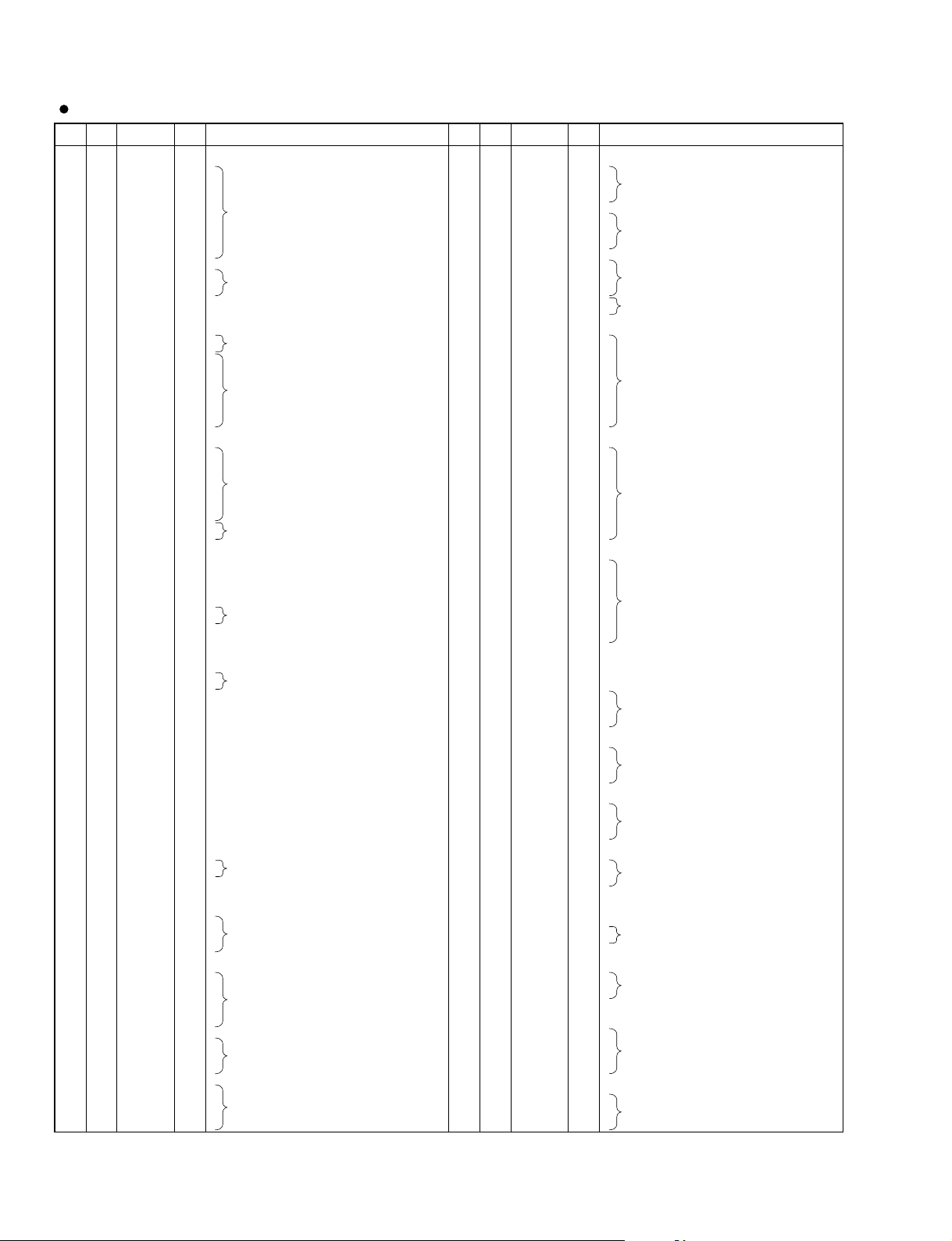
HD6417709SHF200 (X2687A00) CPU (SH3)
PIN
NAME
NO.
1
MD1
2
MD2
3
Vcc(RTC)
4
XTAL2
5
EXTAL2
6
Vss(RTC)
7
NMI
IRQ0/IRL0/PTH0
8
IRQ1/IRL1/PTH1
9
IRQ2/IRL2/PTH2
10
IRQ3/IRL3/PTH3
11
IRQ4/PTH4
12
D31/PTB7
13
D30/PTB6
14
D29/PTB5
15
D28/PTB4
16
D27/PTB3
17
D26/PTB2
18
VssQ
19
D25/PTB1
20
VccQ
21
D24/PTB0
22
D23/PTA7
23
D22/PTA6
24
D21/PTA5
25
D20/PTA4
26
Vss
27
D19/PTA3
28
Vcc
29
D18/PTA2
30
D17/PTA1
31
D16/PTA0
32
VssQ
33
D15
34
VccQ
35
D14
36
D13
37
D12
38
D11
39
D10
40
41
42
43
44
VssQ
45
46
VccQ
47
48
49
50
51
52
53
54
55
56
VssQ
57
58
VccQ
59
60
61
62
63
64
A10
65
A11
66
A12
67
A13
68
VssQ
69
A14
70
VccQ
71
A15
72
A16
73
A17
74
A18
75
A19
76
A20
77
A21
78
Vss
79
A22
80
Vcc
81
A23
82
VssQ
83
A24
84
VccQ
85
A25
86
BS/PTK4
87
88
WE0/DQMLL
89
WE1/DQMLU/WE
90
WE2/DQMUL/ICIORD/PTK6
91
WE3/DQMUU/ISIOWR/PTK7
92
RD/WR
93
AUDSYNC/PTE7
94
VssQ
95
CS0/MCS0
96
VccQ
97
CS2/PTK0
98
CS3/PTK1
99
CS4/PTK2
100
CS5/CE1A/PTK3
101
CS6/CE1B
102
CE2A/PTE4
103
CE2B/PTE5
104
RD
I/O
I
Mode control
I
-
O
I
I
I
I
I
I
I
I/O
I/O
I/O
I/O
I/O
I/O
-
I/O
I/O
I/O
I/O
I/O
I/O
I/O
I/O
I/O
I/O
I/O
I/O
I/O
I/O
I/O
I/O
I/O
D9
I/O
D8
I/O
D7
I/O
D6
D5
D4
D3
D2
D1
D0
A0
A1
A2
A3
A4
A5
A6
A7
A8
A9
I/O
I/O
I/O
I/O
I/O
I/O
I/O
I/O
I/O
I/O
I/O
I/O
I/O
I/O
I/O
I/O
-
-
O
O
O
O
-
O
-
O
O
O
O
O
O
O
O
O
-
O
-
O
O
O
O
O
O
O
-
O
-
O
-
O
-
O
O
O
O
O
-
O
-
O
Power supply +1.8 V
Crystal oscillator
Ground
Non-maskable interrupt request
Interrupt request / Port H
Data bus / Port B
Ground
Data bus / Port B
Power supply +3.3 V
Data bus / Port B
Data bus / Port A
Ground
Data bus / Port A
Power supply +1.8 V
Data bus / Port A
Ground
Data bus
Power supply +3.3 V
Data bus
Ground
Data bus
Power supply +3.3 V
Data bus
Address bus
Ground
Address bus
Power supply +3.3 V
Address bus
Ground
Address bus
Power supply +3.3 V
Address bus
Ground
Address bus
Power supply +1.8 V
Address bus
Ground
Address bus
Power supply +3.3 V
Address bus
Bus cycle / Port K
Read strobe
Select signal (D7-D0) / D QM (SDRAM)
Select signal (D15-D8) / D QM (SDRAM) / Write enable
Select signal (D23-D16) / D QM (SDRAM) / I/O read / Port K
Select signal (D31-D24) / D QM (SDRAM) / I/O write / Port K
Read / Write
AUD cycle / Port E
Ground
Chip select / Mask ROM chip select
Power supply +3.3V
Chip select / Port K
Chip select / Chip enable / Port K
Chip select / Chip enable
Chip enable / Port E
FUNCTION
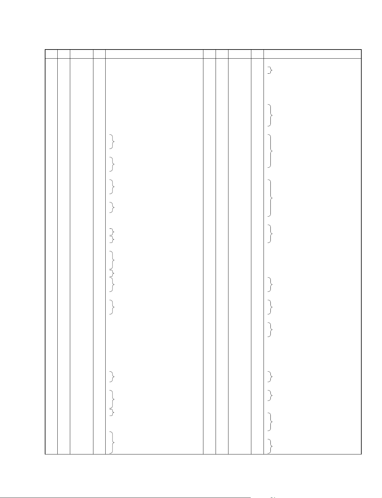
PIN
NAME
NO.
105
CKE/PTK5
106
RAS3L/PTJ0
107
PTJ1
108
CASL/PTJ2
109
VssQ
110
CASU/PTJ3
111
VccQ
112
PTJ4
113
PTJ5
DACK0/PTD5
114
DACK1/PTD7
115
PTE6
116
PTE3
117
RAS3U/PTE2
118
PTE1
119
TDO/PTE0
120
BACK
121
BREQ
122
WAIT
123
RESETM
124
ADTRG/PTH5
125
IOIS16/PTG7
126
ASEMD0/PTG6
127
ASEBRKAK/PTG5
128
PTG4/CKIO2
129
AUDATA3/PTG3
130
AUDATA2/PTG2
131
Vss
132
AUDATA1/PTG1
133
Vcc
134
AUDATA0/PTG0
135
TRST/PTF7/PINT15
136
TMS/PTF6/PINT14
137
TDI/PTF5/PINT13
138
TCK/PTF4/PINT12
139
IRLS3/PTF3/PINT11
140
IRL2/PTF2/PINT10
141
IRLS1/PTF1/PINT9
142
IRLS0/PTF0/PINT8
143
MD0
144
Vcc(PLL1)
145
CAP1
146
Vss(PLL1)
147
Vss(PLL2)
148
CAP2
149
VCC(PLL2)
150
AUDCK/PTH6
151
Vss
152
Vss
153
Vcc
154
XTAL1
155
EXTAL1
156
STATUS0/PTJ6
157
STATUS1/PTJ7
158
TCLK/PTH7
159
/IRQOUT
160
VssQ
161
CKIO
162
VccQ
163
TXD0/SCPT0
164
SCK0/SCPT1
165
TXD1/SCPT2
166
SCK1/SCPT3
167
TXD2/SCPT4
168
SCK2/SCPT5
169
RTS2/SCPT6
170
RXD0/SCPT0
171
RXD1/SCPT2
172
Vss
173
RXD2/SCPT4
174
Vcc
175
CTS2/IRQ5/SCPT7
176
MCS7/PTC7/PINT
177
178
MCS6/PTC6/PINT
179
180
MCS5/PTC5/PINT
181
182
MCS4/PTC4/PINT
183
184
VssQ
185
WAKEUP/PTD3
186
VccQ
187
RESETOUT/PTD2
188
MCS3/PTC3/PINT
189
190
MCS2/PTC2/PINT
191
192
MCS1/PTC1/PINT
193
194
MCS0/PTC0/PINT
195
196
DRAK0/PTD1
197
DRAK1/PTD0
198
DREQ0/PTD4
199
DREQ1/PTD6
200
RESETP
201
CA
202
MD3
203
MD4
204
MD5
205
AVss
206
AN0/PTL0
207
AN1/PTL1
208
DM: IC014
I/O
I/O
I/O
I/O
I/O
-
I/O
I/O
I/O
I/O
I/O
I/O
I/O
I/O
I/O
I/O
O
I
I
I
I
I
I
I/O
I/O
I/O
I/O
-
I/O
-
I/O
I
I
I
I
I
I
I
I
I
-
-
-
-
-
-
I
-
-
-
O
I
I/O
I/O
I/O
O
-
I/O
-
O
I/O
O
I/O
O
I/O
I/O
I
I
I
-
I
I/O
I/O
7
I/O
I/O
6
-
I/O
5
-
I/O
4
I/O
I/O
I/O
I/O
I/O
I/O
3
I
I
2
I
I
1
I
I
0
I
-
I
I
I
I
I
I
I/O
I/O
-
CK enable / Port K
RAS address bus / Port J
Port J
CAS address bus / Port J
Ground
CAS address bus / Port J
Power supply +3.3 V
Port J
DMA acknowledge / Port D
Port E
RAS address bus / Port E
Port E
Test data / Port E
Bus acknowledge
Bus request
Hardware wait request
Manual reset
Analog trigger / Port H
Write protect / Port G
ASE mode / Port G
ASE break acknowledge / Port G
Port G / Clock output
AUD data / Port G
Ground
AUD data / Port G
Power supply +1.8 V
AUD data / Port G
Test reset / Port F / Port interruption
Test mode switch / Port F / Port interruption
Test data / Port F / Port interruption
Test clock / Port F / Port interruption
Interrupt request / Port F / Port interruption
Mode control
Power supply +1.8 V
Capacitor
Ground
Ground
Capacitor
Power supply +1.8 V
AUD clock / Port H
Ground
Power supply +1.8 V
Crystal oscillator
Processor status / Port J
Timer clock / Port H
Interrupt request output
Ground
System clock input / output
Power supply +3.3 V
Data transmission / SCI port
Serial clock / SCI port
Data transmission / SCI port
Serial clock / SCI port
Data transmission / SCI port
Serial clock / SCI port
Transmit request / SCI port
Data reception / SCI port
Ground
Data reception / SCI port
Power supply +1.8 V
Transmit clear / Interrupt request / SCI port
Mask ROM chip select / Port C / Port interruption
Ground
Standby mode Interrupt request output / Port D
Power supply +3.3 V
Reset output / Port D
Mask ROM chip select / Port C / Port interruption
DMA acknowledge / Port D
DMA request / Port D
Power on reset
Chip active
Mode control
Analog ground
Analog input / Port L
Analog power supply +3.3 V
Analog input / Analog output / Port L
Analog ground
FUNCTION
19
CLP-150/CLP-150M/CLP-150C
T8F02TB-0102 (X0060A00) SWP50 (Tone Generator)
PIN
NO.
100
101
102
103
104
105
OUTER
1
2
3
4
5
6
7
8
9
10
11
12
13
14
15
16
17
18
19
20
21
22
23
24
25
26
27
28
29
30
31
32
33
34
35
36
37
38
39
40
41
42
43
44
45
46
47
48
49
50
51
52
53
54
55
56
57
58
59
60
61
62
63
64
65
66
67
68
69
70
71
72
73
74
75
76
77
78
79
80
81
82
83
84
85
86
87
88
89
90
91
92
93
94
95
96
97
98
99
NO.
E10
D10
E11
D11
C10
B10
A10
E12
D12
C11
B11
A11
C12
B12
E13
D13
C13
A12
B13
A13
A14
E14
D14
C14
B14
B15
C15
D15
E15
A15
A16
B16
C16
D16
E16
A17
B17
A18
C17
D17
E17
B18
A19
C18
B19
D18
E18
C19
A20
B20
C20
D19
E19
A21
B21
A22
D20
C21
E20
D21
B22
A23
C22
B23
E21
D22
C23
A24
B24
A25
E5
D4
C3
B2
A1
D5
E6
C4
B3
A2
A3
D6
E7
C5
B4
A4
D7
C6
E8
D8
B5
A5
C7
B6
E9
D9
C8
A6
B7
A7
C9
B8
A8
B9
A9
NAME
VSS2
VDDC
CD15
CD13
CD14
CD6
CD2
CD9
CD11
CD12
CD10
CD1
VSS
CD5
CD8
CD7
VSS2
CD0
VSS
VDDS
CD4
CD3
CA2
CA0
CA8
CA9
CA5
CA1
CA3
CA4
VSS2
VDDC
CA10
CA6
CA7
CA11
CA14
CA15
CA13
CA12
CSN0
CSN1
VSS
VDDS
WRN
RDN
WAIT0
IRQ0
DREQ0
TCK
TRST
VSS
VDDS
SLAVE
TMS
TDO
ICN
RFCLK0
PLL_TSTN
PLL_BP
VDDS
VSS
RFCLK1
VDDC
TMODE
PLL_AVD
PLL_AVS
TEST1
VSS
SY1
VDDC
VSS2
KONTRG0
KONTRG1
CK512
CK128
BCLK
SY0
HMA20
HMA21
HMA19
HMA18
VDDS
VSS
HMA9
HMA7
HMA6
HMA8
HMA10
HMA17
VDDS
HMA11
HMA4
HMA5
HMA13
VSS
HMA12
HMA3
HMA14
HMA2
HMA1
XO
NC
NC
I/O
-
I/O
I/O
I/O
I/O
I/O
I/O
I/O
I/O
I/O
I/O
I/O
I/O
I/O
I/O
-
I/O
I/O
I
I
I
I
I
I
I
I
-
-
I
I
I
I
I
I
I
I
I
I
-
-
I
I
O
O
O
I
I
-
O
XI
I
-
I
I
O
I
O
I
I
-
-
I
-
I
-
-
-
-
I
-
I
-
-
O
I
O
O
O
O
O
O
O
O
-
O
O
O
O
O
O
O
O
O
O
O
O
O
O
O
Ground
Power supply +1.5 V
Data bus of internal register
Ground
Data bus of unternal register
Ground
Data bus of unternal register
Ground
Power supply +3 V
Data bus of internal register
Address bus of internal regisuter
Ground
Power supply +1.5 V
Address bus of internal regisuter
Chip select
Ground
Power supply +3 V
Write strobe
Read strobe
Hardware wait request
Interrupt request
Test pin
Ground
Crystal osc. output
Crystal osc. input
Power supply +3 V
Master/Slave select
Test pin
Initial clear
PLL Clock
Power supply
Power supply +3 V
Ground
PLL Clock
Power supply +1.5 V
Test pin
Power supply (PLL)
Not used
Not used
Power supply (PLL)
Test pin
Ground
Sync. clock
Power supply +1.5 V
Ground
Key on data
Master clock (256 Fs)
Master clock (64 Fs)
Sync. clock
Wave memory address bus
Power supply +1.5 V
Ground
Wave memory address bus
Power supply +1.5 V
Wave memory address bus
Ground
Wave memory address bus
FUNCTION
PIN
NO.
106
107
108
109
110
111
112
113
114
115
116
117
118
119
120
121
122
123
124
125
126
127
128
129
130
131
132
133
134
135
136
137
138
139
140
141
142
143
144
145
146
147
148
149
150
151
152
153
154
155
156
157
158
159
160
161
162
163
164
165
166
167
168
169
170
171
172
173
174
175
176
177
178
179
180
181
182
183
184
185
186
187
188
189
190
191
192
193
194
195
196
197
198
199
200
201
202
203
204
205
206
207
208
209
210
OUTER
NO.
E22
D23
C24
B25
A26
E23
F22
D24
C25
B26
C26
F23
G22
E24
D25
D26
G23
F24
H22
H23
E25
E26
G24
F25
J22
J23
H24
F26
G25
G26
K22
K23
J24
H25
H26
J25
L22
L23
K24
J26
K25
K26
M22
M23
L24
L25
L26
M24
M25
N22
N23
N24
M26
N25
N26
P26
P22
P23
P24
P25
R25
R24
R23
R22
R26
T26
T25
T24
T23
T22
U26
U25
V26
U24
U23
U22
V25
W26
V24
W25
V23
V22
W24
Y26
Y25
Y24
W23
W22
AA26
AA25
AB26
Y23
AA24
Y22
AA23
AB25
AC26
AB24
AC25
AA22
AB23
AC24
AD26
AD25
AE26
NAME
VSS2
VDDC
HMA15
HMA16
HMA22
HMA25
VDDS
HMA27
HMA0
HMA23
HMA24
VDDS
HMA26
HMA30
HMA28
HMA29
LMA17
LMA19
VSS
VDDS
LMA20
LMA21
LMA9
LMA18
LMA12
LMA4
LMA6
LMA8
LMA7
LMA10
VSS2
VDDC
LMA13
LMA11
LMA5
LMA3
LMA16
LMA0
LMA2
LMA14
LMA15
LMA1
VSS
VDDS
LMA22
LMA23
LMA24
LMA27
LMA28
LMA25
LMA26
LMA30
LMA29
MOEN
MWEN
LMD15
VSS
VDDS
LMD13
LMD14
LMD11
LMD10
VDDS
VSS
LMD12
LMD9
LMD8
LMD7
VSS2
VSS
LMD6
LMD5
LMD3
LMD4
VDDC
VSS2
LMD2
LMD0
LMD1
DCSL0
VDDS
VDDC
DCSL1
DQML3
DQML1
DMAL14
VDDS
VSS
DMAL13
DMAL12
DMAL9
VSS
DMAL11
VSS
DMAL10
DMAL8
DMAL6
DMAL7
DMAL5
VSS2
VSS
DMAL4
DMAL3
DMAL2
DMAL0
I/O
I/O
I/O
I/O
I/O
I/O
I/O
I/O
I/O
I/O
I/O
I/O
I/O
I/O
I/O
I/O
I/O
DM: IC012
FUNCTION
-
O
O
O
O
O
O
O
O
O
O
O
O
O
O
-
O
O
O
O
O
O
O
O
O
O
-
O
O
O
O
O
O
O
O
O
O
-
O
O
O
O
O
O
O
O
O
O
O
-
-
-
-
-
-
-
-
O
-
O
O
O
O
-
O
O
O
O
O
O
O
O
O
-
O
O
O
O
Ground
Power supply +1.5 V
Wave memory address bus
Power supply +3 V
Wave memory address bus
Power supply +3 V
Wave memory address bus
Wave memory address bus (Lower data memory)
Ground
Power supply +3 V
Wave memory address bus (Lower data memory)
Ground
Power supply +1.5 V
Wave memory address bus (Lower data memory)
Ground
Power supply +3 V
Wave memory address bus (Lower data memory)
Wave memory output enable
Wave memory write enable
Wave memory data bus (Lower 16 bit)
Ground
Power supply +3 V
Wave memory data bus (Lower 16 bit)
Power supply +3 V
Ground
Wave memory data bus (Lower 16 bit)
Ground
Ground
Wave memory data bus (Lower 16 bit)
Power supply +3 V
Ground
Wave memory data bus (Lower 16 bit)
Power supply +3 V
Power supply +1.5 V
MASK signal
Address bus (DIMM, SDRAM)
Power supply +3 V
Ground
Address bus (DIMM, SDRAM)
Ground
Address bus (DIMM, SDRAM)
Ground
Address bus (DIMM, SDRAM)
Ground
Ground
Address bus (DIMM, SDRAM)
20
CLP-150/CLP-150M/CLP-150C
PIN
NO.
211
212
213
214
215
216
217
218
219
220
221
222
223
224
225
226
227
228
229
230
231
232
233
234
235
236
237
238
239
240
241
242
243
244
245
246
247
248
249
250
251
252
253
254
255
256
257
258
259
260
261
262
263
264
265
266
267
268
269
270
271
272
273
274
275
276
277
278
279
280
281
282
283
284
285
286
287
288
289
290
291
292
293
294
295
296
297
298
299
300
301
302
303
304
305
306
307
308
309
310
311
312
303
314
315
OUTER
NO.
AB22
AC23
AD24
AE25
AF26
AC22
AB21
AD23
AE24
AF25
AF24
AC21
AB20
AD22
AE23
AF23
AC20
AD21
AB19
AC19
AE22
AF22
AD20
AE21
AB18
AC18
AD19
AF21
AE20
AF20
AB17
AC17
AD18
AE19
AF19
AE18
AB16
AC16
AD17
AF18
AE17
AF17
AB15
AC15
AD16
AE16
AF16
AD15
AE15
AB14
AC14
AD14
AF15
AE14
AF14
AF13
AB13
AC13
AD13
AE13
AE12
AD12
AC12
AB12
AF12
AF11
AE11
AD11
AC11
AB11
AF10
AE10
AF9
AD10
AC10
AB10
AE9
AF8
AD9
AE8
AC9
AB9
AD8
AF7
AE7
AD7
AC8
AB8
AF6
AE6
AF5
AC7
AD6
AB7
AC6
AE5
AF4
AD5
AE4
AB6
AC5
AD4
AF3
AE3
AF2
NAME
VSS2
VDDC
DMAL1
DCSL2
DRAS0
DCAS0
VDDS
DCLKIN
DQML2
DCSL3
DQML0
VDDS
VSS
DWEN0
DCLK0
DCLK1
DCLKE
HMD13
VSS
VDDS
HMD15
HMD14
HMD10
HMD12
VDDC
VDDS
HMD7
HMD11
HMD9
HMD8
VSS2
VDDC
HMD4
HMD6
HMD5
HMD3
VSS
VSS2
HMD1
HMD2
HMD0
DCSH0
VSS
VDDS
DCSH1
DQMH3
DQMH1
DMAH14
DMAH13
VSS
VSS2
DMAH11
DMAH12
DMAH10
DMAH9
DMAH8
VDDS
VDDS
DMAH6
DMAH7
DMAH4
DMAH3
VDDS
VSS
DMAH5
DMAH2
DMAH1
DMAH0
VSS
VSS
DRAS1
DCSH2
DQMH2
DCSH3
VDDC
VSS2
DQMH0
DWEN1
DCAS1
DCLK2
VDDS
VDDC
DCLK3
MELO0
MELO1
MELO2
VDDS
VSS
MELO3
MELO4
MELO5
MELO6
MELO7
WCLK0
WCLK1
EIRQ
EICN
ESDA
ESCL
MELI0
MELI1
MELI2
MELI3
MELI4
MELI5
I/O
I/O
I/O
I/O
I/O
I/O
I/O
I/O
I/O
I/O
I/O
I/O
I/O
I/O
I/O
I/O
I/O
I/O
I/O
PIN
FUNCTION
-
O
O
O
O
-
I
O
O
O
-
O
O
O
O
-
-
Ground
Power supply +1.5 V
Address bus (DIMM, SDRAM)
Power supply +3 V
MASK signal
MASK signal
Power supply +3 V
Ground
Wave memory data bus (Upper data memory)
Ground
Power supply +3 V
Wave memory data bus (Upper data memory)
-
-
Power supply +1.5 V
Power supply +3 V
Wave memory data bus (Upper data memory)
-
-
Ground
Power supply +1.5 V
Wave memory data bus (Upper data memory)
-
-
Ground
Ground
Wave memory data bus (Upper data memory)
O
-
O
O
O
O
O
-
O
O
O
O
O
-
O
O
O
O
-
O
O
O
O
-
O
O
O
O
-
O
O
O
O
-
O
O
O
O
-
O
O
O
O
O
O
O
O
O
I
I
I
I
I
I
Ground
Power supply +3 V
MASK signal
Address bus (DIMM, SDRAM)
Ground
Ground
Address bus (DIMM, SDRAM)
Power supply +3 V
Power supply +3 V
Address bus (DIMM, SDRAM)
Power supply +1.5 V
Ground
Address bus (DIMM, SDRAM)
Ground
Ground
MASK signal
Power supply +1.5 V
Ground
MASK signal
Power supply +3 V
Power supply +1.5 V
MEL wave data output
Ground
MEL wave data output
For DAC LR clock
MEL wave data input
NO.
316
317
318
319
320
321
322
323
324
325
326
327
328
329
330
331
332
333
334
335
336
337
338
339
340
341
342
343
344
345
346
347
348
349
350
351
352
353
354
355
356
357
358
359
360
361
362
363
364
365
366
367
368
369
370
371
372
373
374
375
376
377
378
379
380
381
382
383
384
385
386
387
388
389
390
391
392
393
394
395
396
397
398
399
400
401
402
403
404
405
406
407
408
409
410
411
412
413
414
415
416
417
418
419
420
OUTER
NO.
AB5
AC4
AD3
AE2
AF1
AB4
AA5
AC3
AD2
AE1
AD1
AA4
AB3
AC2
AC1
AA3
W5
W4
AB2
AB1
AA2
W3
AA1
W2
W1
M2
M3
M4
M5
M1
U5
U4
U3
U2
U1
R5
R4
R3
R2
R1
N1
N5
N4
N3
N2
H1
H2
H3
G1
G2
G3
H4
H5
G4
G5
D1
D2
D3
C1
C2
NAME
VSS2
VDDC
MELI6
MELI7
ADLR
DITO
VSS
AFRM
ACLK
ADIR
ADAT0
VDDS
Y5
ADAT9
ADAT3
ADAT1
ADAT2
Y4
ADAT10
ADAT6
VSS
VDDS
ADAT4
ADAT5
Y3
ADAT11
ADAT7
V5
ADAT14
V4
ADAT15
ADAT13
ADAT8
Y2
ADAT12
Y1
TDI
VSS2
VDDC
V3
HRD13
HRD15
HRD14
V2
HRD12
T5
HRD7
T4
HRD6
HRD10
V1
HRD11
HRD9
HRD8
VSS
VDDS
T3
HRD5
T2
HRD4
T1
HRD3
HRD2
HRD1
P5
VDDS
P4
HRD0
P3
RWEN
RQML
P2
RCAS
P1
RRAS
RA13
VDDS
VDDS
RA10
RA12
RA1
RA2
VDDS
VSS
RA0
L1
RA3
L2
RA4
L3
RA5
L4
VSS2
L5
VSS
K1
RA6
K2
RA7
J1
RA9
K3
RA8
K4
VDDC
K5
VSS2
J2
RA11
RCLK
J3
RCLKE
RCLKIN
J4
VDDS
J5
VDDC
RQMH
LRD15
LRD14
LRD13
VDDS
VSS
F1
LRD12
F2
LRD11
E1
LRD8
VDDS
F3
LRD10
VDDS
F4
LRD9
E2
LRD7
LRD5
E3
LRD6
LRD4
F5
VSS2
E4
VSS
LRD3
LRD2
LRD1
B1
LRD0
I/O
I/O
I/O
I/O
I/O
I/O
I/O
I/O
I/O
I/O
I/O
I/O
I/O
I/O
I/O
I/O
I/O
I/O
I/O
I/O
I/O
I/O
I/O
I/O
I/O
I/O
I/O
I/O
I/O
I/O
I/O
I/O
I/O
I/O
I/O
I/O
I/O
I/O
I/O
I/O
I/O
I/O
I/O
I/O
I/O
I/O
I/O
I/O
I/O
I/O
I/O
-
I
I
O
O
-
O
-
Ground
Power supply +1.5 V
MEL wave data input
Power supply +3 V
Ground
Data bus (ABUS)
Power supply +3 V
FUNCTION
Data bus (ABUS)
-
-
Ground
Power supply +3 V
Data bus (ABUS)
I
-
-
Ground
Power supply +1.5 V
DRAM data bus
-
-
Ground
Power supply +3 V
DRAM data bus
-
O
O
O
O
O
-
O
O
O
O
-
O
O
O
O
-
O
O
O
O
-
O
O
O
I
-
O
Power supply +3 V
DRAM data bus
DRAM write enable
DRAM column address strobe (RAS signal)
DRAM row address strobe (RAS signal)
DRAM address bus
Power supply +3 V
Power supply +3 V
DRAM address bus
Power supply +3 V
Ground
DRAM address bus
Ground
Ground
DRAM address bus
Power supply +1.5 V
Ground
DRAM address bus
Power supply +3 V
Power supply +1.5 V
DRAM data bus (Lower data)
-
-
Power supply +3 V
Ground
DRAM data bus (Lower data)
-
-
Ground
DRAM data bus (Lower data)
Ground
DRAM data bus (Lower data)
-
-
Ground
Ground
DRAM data bus (Lower data)
21
CLP-150/CLP-150M/CLP-150C
M66291GP (X2156A00) USB Controller
PIN
NO.
1
2
3
4
5
6
7
8
9
10
11
12
13
14
15
16
17
18
19
20
21
22
23
24
Core Vcc
GND
D-
D+
Vbus
Tr ON
TEST
/Dack1
/Dreq1
/TC1
/INT1//SOF
IOVcc
Xout
Xin
GND
Core Vcc
A1
A2
A3
A4
A5
A6
D0
D1
I/O FUNCTIONNAME
I/O
I/O
O
O
O
O
I/O
I/O
Core power supply
Ground
USB data (-)
I
I
I
I
I
I
I
I
I
I
I
USB data (+)
V bus input
Tr ON output
TEST input
DMA reception signal 1
DMA request 1
TC input
Interrupt 1/SOF output
I/O power supply
Output for oscillation
Input for oscillation
Ground
Core power supply
Address bus
Data bus
PIN
NO.
25
26
27
28
29
30
31
32
33
34
35
36
37
38
39
40
41
/HWR//BYTE
42
43
44
45
46
47
48
D2
D3
D4
D5
D6
D7
D8/P0
D9/P1
D10/P2
D11/P3
IOVcc
GND
D12/P4
D13/P5
D14/P6
D15/A0
/INT0
/RD
/LWR
/CS
/RST
/Dreq0
/Dack0
I/O FUNCTIONNAME
I/O
I/O
I/O
I/O
I/O
I/O
I/O
I/O
I/O
I/O
I/O
I/O
I/O
I/O
I
O
I
I
I
I
O
I
PCM1730E-1/2K (X2077A00) DAC (Digital to Analog Converter)
PIN
NO.
10
11
12
13
14
1
2
ZEROL
3
ZEROR
4
5
6
7
8
DGND
9
DEPMP0
DEMP1
/RST
LRCK
DATA
BCK
SCKI
VDD
FMT0
FMT1
FMT2
I/O FUNCTIONNAME
I
O
O
I
I
I
I
-
-
I
I
I
I
I
Reset
Zero flag for L-channel
Zero flag for R-channel
Left and right clock
Serial audio data input
Bit clock input
System clock input
Digital ground
Digital supply, +3.3V
De-emphasis control
Audio data format select
PIN
NO.
15
16
17
18
19
20
21
22
23
24
25
26
27
28
MUTE
IOUTR-
IOUTR+
AGND1
VCOM1
VCOM2
IREF
VCOM3
VCC1
VCC2
IOUTL+
IOUTLAGND2
VCC3
I/O FUNCTIONNAME
I
O
O
-
-
-
-
-
-
O
O
I
I
DM: IC002
Data bus
I/O power supply
Ground
Data bus
Highlight strobe/bus width select
Interrupt 0
Read strobe
Low write strobe
Chip select
Reset signal
DMA request 0
DMA reception signal 0
DM: IC029
Analog output mute control
R-channel analog current output R-channel analog current output +
Analog ground
Internal bias de-coupling pin
Common voltage for I/V
Output current reference bias pin
Internal bias de-coupling pin
Analog supply, +5 V
Analog supply, +5 V
L-channel analog current output +
L-channel analog current output Analog ground
Analog power supply, +5 V
22
TC74VHC14FT
(XV890A00)
Hex Inverter
DM: IC006
1
2
3
4
5
6
7
1A
1Y
2A
2Y
3A
3Y
GND
14
13
12
11
10
9
8
VDD
6A
6Y
5A
5Y
4A
4Y
TC74VHC32FT
(XY945A00)
74VHC32MTCX
(X0299A00)
Quad 2 Input OR
DM: IC007
1
2
3
1A
1Y
4
2A
5
2B
6
2Y
7
GND
1B
14
13
12
Vcc
4A
11
4Y
10
3B
9
3A
8
3Y
4B
TC74VHCT245AFT
(XT744A00)
74VHCT245AMTCX
(X0295A00)
Octal 3-State Bus Transceiver
DM: IC009, 010
1
2
3
4
5
6
7
20
19
18
17
16
15
14
Vcc
G
B1
B2
B3
B4
B5
B6
B7
B8
8
9
10
12
11
GND
A8
A7
A6
A5
A4
A3
A2
A1
D1R
13
SN75C1168NSR
(XU073A00)
Line Driver / Receiver
DJK: IC002
1
2
3
4
5
6
7
1B
1A
1R
1DE
2R
2A
2B
16
15
14
13
12
11
10
Vcc
1D
1Y
1Z
2DE
2Z
2Y
8
GND
9
2D
SC7SU04FEL (XI348A00)
TC7SU04F (XY447A00)
Inverter Gate
DJK: IC001
1
2
3
5
4
NC
VSS
VDD
OUT
IN
M5229FP (XY487A00)
7 Band Graphic Equalizer
AJK: IC300, 400
LA6517M-TE-R (XT131A00)
Dual Low Voltage Power Amplifier
AJK: IC200
1
2
3
4
5
6
7
8
16
15
14
13
12
11
10
9
Thermal Shut
Doun and
Current Limiter
Amp1
Amp2
NC
NC
OUT 1
VCC
OUT 2
VEE
NC
NC
NC
NC
INPUT -2
INPUT +2
INPUT +1
INPUT -1
NC
NC
µPC4570G2 (XF291A00)
Dual Operational Amplifier
DM: IC033-35
AJK: IC100
PNL: IC073
1
2
3
4-V
8
7
6
5
Output 1
+V
+Input 1
VEE
VCC
Output 2
-Input 2
+Input 2
-Input 1
+-
+-
TC7WH32FU(TE12L) (XY364A00)
Dual 2 Input OR Gate
DM: IC013
1
2
3
4
8
7
6
5
1A
2Y
GND
Vcc
1Y
2B
2A
1B
■ IC BLOCK DIAGRAM
CLP-150/CLP-150M/CLP-150C
23
CLP-150/CLP-150M/CLP-150C
■ CIRCUIT BOARDS
AJK (X2246B0) . . . . . . . . . . . . . . . . . . . . . . . . . . . . 25
DJK (X2245C0) . . . . . . . . . . . . . . . . . . . . . . . . . . . . 28
DM (XZ592H0) . . . . . . . . . . . . . . . . . . . . . . . . . 26/27
FU120L (XS882A0) . . . . . . . . . . . . . . . . . . . . . . . . . 33
GHD EBUS L (XZ138D0) . . . . . . . . . . . . . . . . . . . .35
GHD H (X2218A0) . . . . . . . . . . . . . . . . . . . . . . . . . 37
GHD M (X2217A0) . . . . . . . . . . . . . . . . . . . . . . . . .36
HP (XQ390A0) . . . . . . . . . . . . . . . . . . . . . . . . . . . . 32
MA120 (XQ393E0) . . . . . . . . . . . . . . . . . . . . . . . . . 29
MK SUB (XZ142B0) . . . . . . . . . . . . . . . . . . . . . . . .34
MV2 (X2244B0) . . . . . . . . . . . . . . . . . . . . . . . . . . . . 32
NET1 (XT123B0) . . . . . . . . . . . . . . . . . . . . . . . . . . . 29
PEDAL (DJK) (X2245C0) . . . . . . . . . . . . . . . . . . . .28
PEDAL (SW) (X0193A0) . . . . . . . . . . . . . . . . . . . . . 34
PL (XR898A0) . . . . . . . . . . . . . . . . . . . . . . . . . . . . .32
PNL (X2243D0) . . . . . . . . . . . . . . . . . . . . . . . . . 30/31
PNR (X2244B0) . . . . . . . . . . . . . . . . . . . . . . . . 32/33
WML (X2248A0) . . . . . . . . . . . . . . . . . . . . . . . . . . .24
WMH (X2248A0) . . . . . . . . . . . . . . . . . . . . . . . . . . .24
Note : See parts list for details of circuit board conponent parts.
WML Circuit Board
WMH Circuit Board
to DM-CN14 (WML)
to DM-CN15 (WMH)
Component side
24
Pattern side
2NA-V856300
AJK Circuit Board
to MA120-CN6
to DM-CN24to MV2-CN20
CLP-150/CLP-150M/CLP-150C
to HP-CN1to MA120-CN4
Component side
Pattern side
25
CLP-150/CLP-150M/CLP-150C
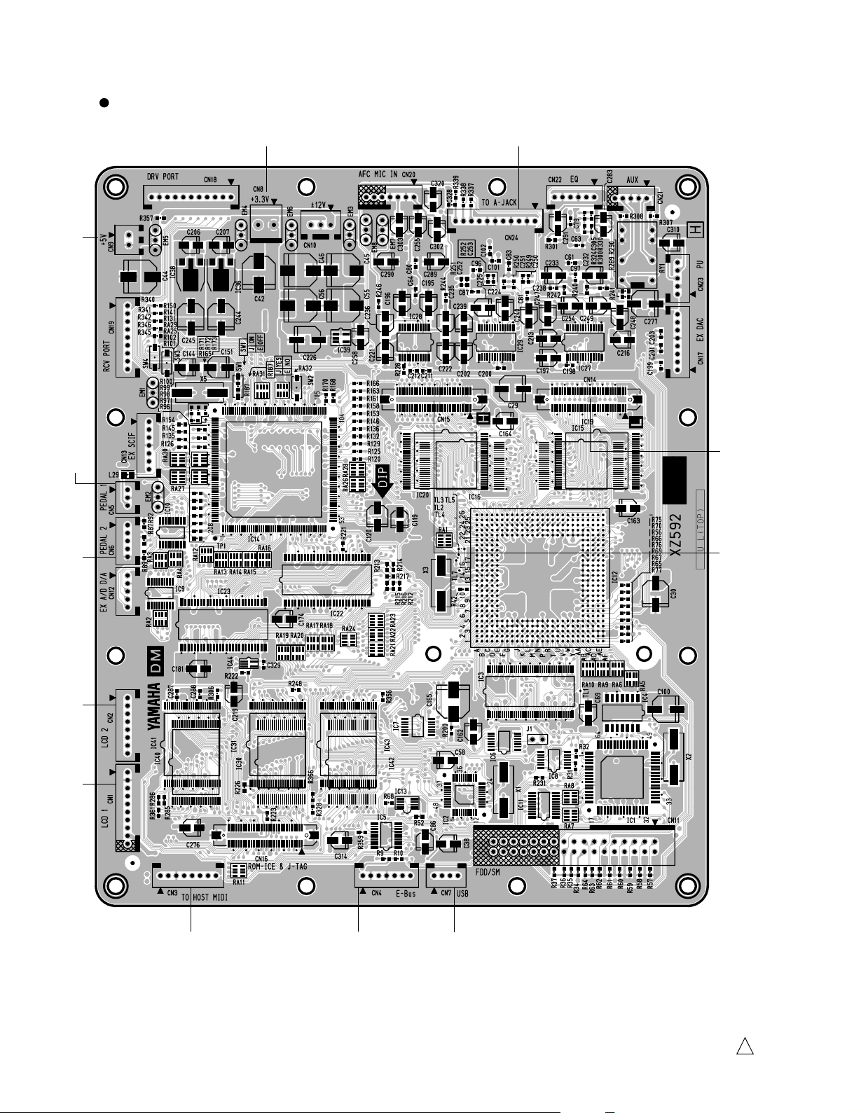
DM Circuit Board (XZ592H0)
to MA120-CN3to PEDAL-CN11to PNR-CN92to PNR-CN91 to DJK-CN1
to DJK-CN8
to AJK-CN500
to WML-CN1to WMH-CN1
26
to DJK-CN5
to PNL-CN101,
GHD EBUS L-CN1
to DJK-CN6
Component side
2NA-V755310
2
DM Circuit Board (XZ592H0)
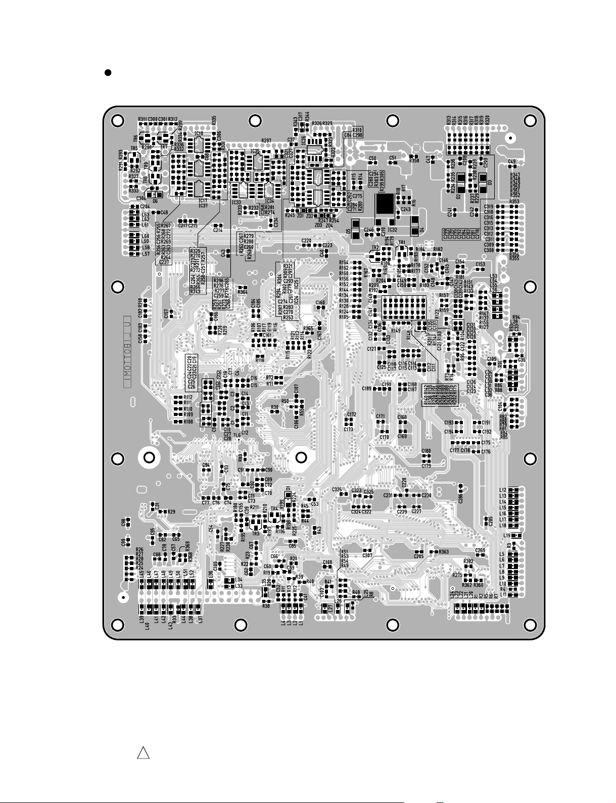
CLP-150/CLP-150M/CLP-150C
2NA-V755310
Pattern side
2
27
CLP-150/CLP-150M/CLP-150C
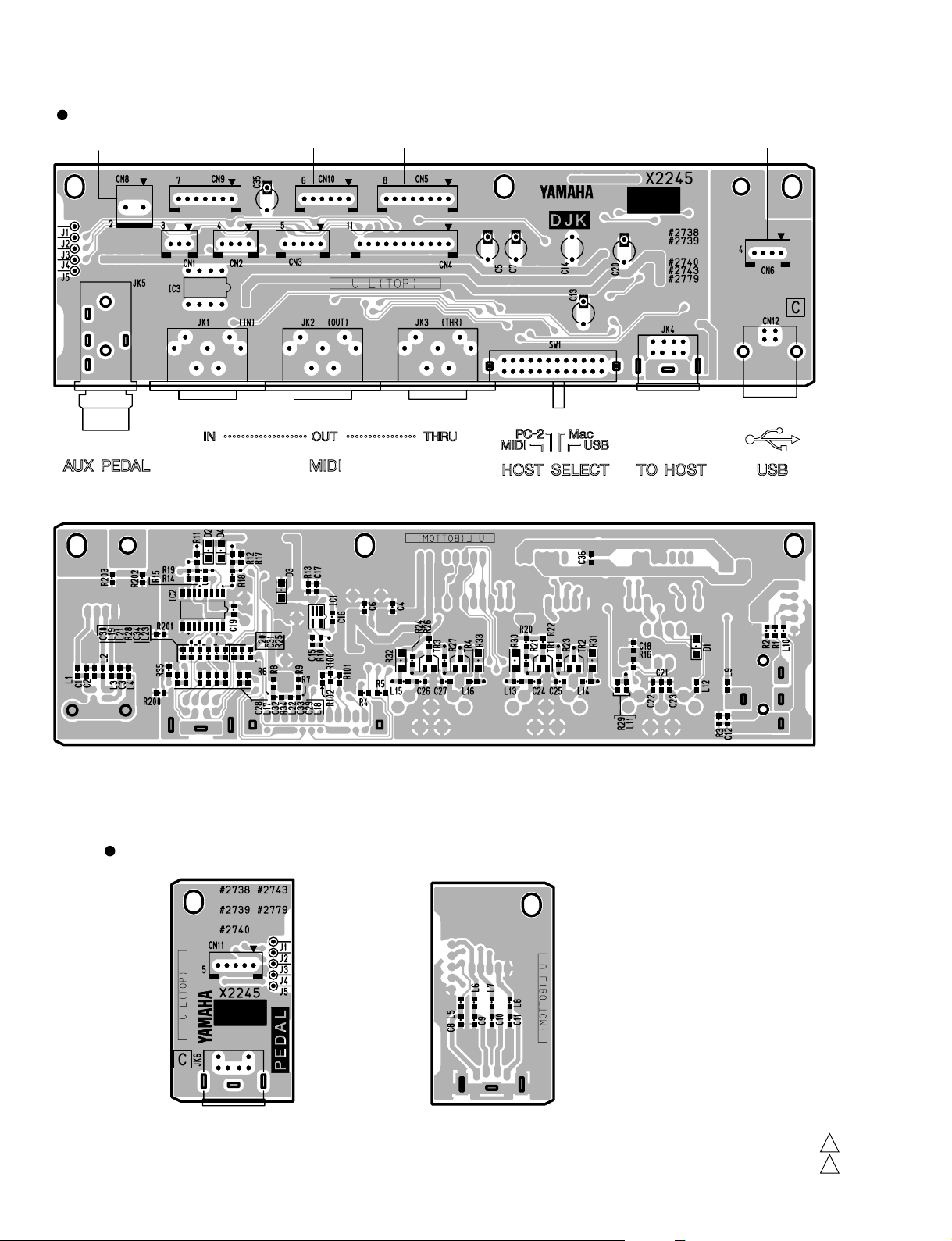
DJK Circuit Board
to DM-CN5
to MA120-CN4
to DM-CN3 to DM-CN7to DM-CN8
Component side
28
PEDAL (DJK) Circuit Board
to DM-CN6
Component side
to PEDAL (SW)-CN1
Pattern side
DJK: 2NA-V849640
PEDAL (DJK): 2NA-V849640
Pattern side
2
2

CLP-150/CLP-150M/CLP-150C
MA120 Circuit Board
to AJK-CN520
Q
Q
Q'
Q'
NOTE : The symbol ( ) shows Slow operating fuse.
to DJK-CN10,
AJK-CN540
CAUTION:
5A 125V FUSE.
ATTENTION:
RECHANGE DE MÉME TYPE DE 5A 125V.
REPLACE WITH SAME TYPE
UTILISER UN FUSIBLE DE
N.C.
(Secondary)
to Power Transformer
to DM-CN9
Component side
NET1 Circuit Board
to Woofer and Tweeter Speakers
8
C0002
C0004
CN002
XT123
C0001
J
C0003
J
CN003
15
N.C.
1
4
CN001
1
B
Component side
MA120: 2NA-VT14340
NET1: 2NA-VY64290
3
1
29
CLP-150/CLP-150M/CLP-150C
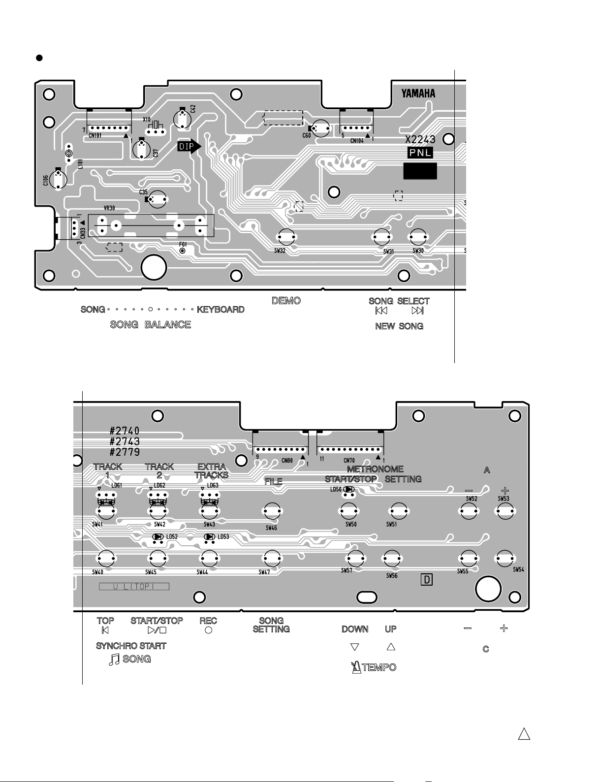
PNL Circuit Board
to DM-CN4 NC
A
A'
A
to PNR-CN81 to PNR-CN71
30
A'
Component side
2NA-V845480
1