

Yamaha A-4000, A-5000 Service manual
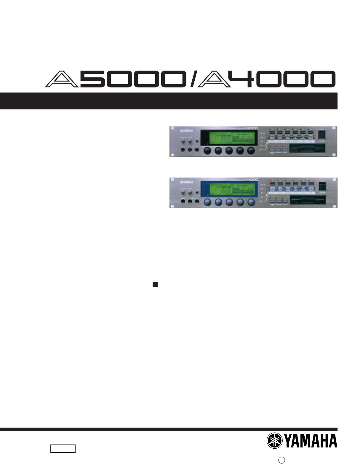
PROFESSIONAL SAMPLER
SERVICE MANUAL
SY 011491
A5000 19991210-229000
A4000 19991210-149000
CONTENTS
SPECIFICA TIONS ................................................................................3
PANEL LAYOUT ..................................................................................4
CIRCUIT BOARD LAYOUT ...................................................................5
BLOCK DIAGRAM ...............................................................................6
DISASSEMBL Y PROCEDURE ............................................................7
LSI PIN DESCRIPTION ......................................................................1 0
IC BLOCK DIAGRAM .........................................................................16
TEST PROGRAM ............................................................................. 19
ERROR MASSAGE ...........................................................................3 1
MIDI DAT A FORMA T ..........................................................................3 2
MIDI IMPLEMENT A TION CHART ........................................................4 3
PA RTS LIST
OVERALL CIRCUIT DIAGRAM
CIRCUIT BOARDS
HAMAMATSU,JAPAN
1.57K-859 I Printed in Japan2000.01
A5000/A4000
This manual has been provided for the use of authorized Yamaha Retailers and their service personnel. It has been
assumed that basic service procedures inherent to the industry, and more specifically Yamaha Products, are
already known and understood by the users, and have therefore not been restated.
WARNING: Failure to follow appropriate service and safety procedures when servicing this product may
IMPORTANT: This presentation or sale of this manual to any individual or firm does not constitute authoriza-
The data provided is believed to be accurate and applicable to the unit(s) indicated on the cover. The research
engineering, and service departments of Yamaha are continually striving to improve Yamaha products. Modifications are, therefor, inevitable and changes in specification sre subject to change without notice or obligation to
retrofit. Should any discrepancy appear to exist, please contact the distributor's Service Division.
WARNING: Static discharges can destroy expensive components. Discharge any static electricity your
IMPORTANT NOTICE
result in personal injury, destruction of expensive components and failure of the product to per
form as specified. For these reasons, we advise all Yamaha product owners that all service
required should be performed by an authorized Yamaha Retailer or the appointed service
repre sentative.
tion, certification, recognition of any applicable technical capabilities, or establish a principalagent relationship of any form.
body may have accumulated by grounding yourself to the ground buss in the unit (heavy gauge
black wires connect to this buss).
IMPORTANT: Turn the unit OFF during disassembly and parts replacement. Recheck all work before you
apply power to the unit.
WARNING: CHEMICAL CONTENT NOTICE!
The solder used in the production of this product contains LEAD. In addition, other electrical / electronic and / or
plastic (where applicable) components may also contain traces of chemicals found by the California Health and
Welfare Agency (and possibly other entities) to cause cancer and / or birth defects or other reproductive harm.
DO NOT PLACE SOLDER, ELECTRICAL / ELECTRONIC OR PLASTIC COMPONENTS IN YOUR MOUTH FOR ANY
REASON WHAT SO EVER!
Avoid prolonged, unprotected contact between solder and your skin! When soldering, do not inhale solder fumes or
expose eyes to solder / flux vapor!
If you come in contact with solder or components located inside the enclosure of this product, wash your hands
before handling food.
WARNING
Components having special characteristics are marked and must be replaced with parts having specification equal to those
originally installed.

SPECIFICATION
A5000/A4000
Tone generation method
AWM2 tone generator
Maximum Polyphony
126 notes (64 notes on the A4000), 32 multi-timbre parts (16 parts on the A4000)
A/D conversion
20 bit 64-times oversampling
D/A conversion
24 bit 8-times oversampling
Digital I/O (only when AIEB1 I/O expansion board is installed)
Input/output DIGITAL connectors S/P-DIF (coaxial)
OPTICAL connectors S/P-DIF (optical)
Input frequency 48 kHz, 44.1 kHz, 32 kHz
Output frequency 44.1 kHz
Sampling frequency
Analog input 44.1, 22.05, 11.025 kHz, 5.5125 kHz (mono and stereo)
Digital input (only when AIEB1 I/O expansion board is installed)
48 kHz, 44.1 kHz, 32 kHz external synchronized recording
(stereo only)
1/2, 1/4 and 1/8 undersampling is supported
Internal sample memory capacity
Standard 4 Mbytes (installed on-board)
Maximum 128 Mbytes
(When four 32 Mbyte 72 pin SIMM modules are installed. The onboard 4 Mbytes are unused only if memory has been expanded to the
maximum.)
Sampling time
Maximum sample length
32 Mbytes monaural
64 Mbytes stereo
Maximum sampling time (mono or stereo)
6 minutes 20 seconds (44.1 kHz)
12 minutes 40 seconds (22.05 kHz)
25 minutes 21 seconds (11.025 kHz)
50 minutes 43 seconds (5.5125 kHz)
Effects
6 effect blocks (3 on the A4000)
Total equalizer (4 bands)
Sample equalizer
Program
128 program
Sequencer
Real-time recording and playback
Front panel
POWER switch
INPUT L,R jacks (phone x 2)
REC VOLUME (L& R shared)
MASTER VOLUME (L&R shared, STEREO OUT & PHONES shared)
PHONES OUTPUT jack
Knobs (1 - 5)
Mode buttons (PLAY, EDIT, REC, DISK, UTILITY)
Function buttons (six buttons)
COMMAND/EXIT button
ASSIGNABLE button
AUDITION button
LCD (320 x 80 dot, LED backlight)
LCD contrast control
3.5" 2HD/2DD dual mode floppy disk drive
Rear panel
STEREO OUT L/MONO, R (phone jack x 2)
ASSIGNABLE OUT L, R (phone jack x 2)
MIDI IN-A/B, OUT, THRU-A/B (IN, OUT, THRU on the A4000)
SCSI (half-pitch, 50-pin)
Expansion board slot
Power supply connector (AC inlet)
Fan
Dimensions
Two-space rackmount unit
W 480 mm x D 461 mm x H 90 mm (18-7/8” x 18-1/8” x 3-9/16”)
Weight
8.0 kg (17l bs 10 oz)
Included items
Power cable x 1
CD-ROM set
(See the separate “Guide for the Accompanying Disks” booklet)
FD x 4
Power Cable for Internal Hard Disk (long) x 1
Power Cable for ZIP Drive (short) x 1
SCSI Cable for Internal Hard Disk x 1
IDE Cable for Internal Hard Disk x 1
Owner’s manual x 1
Options (made by Yamaha)
AIEB1: I/O expansion board
Internal expansion devices (made by other manufacturers)
Expansion memory
(use a pair of identical-size 72pin SIMM modules of the following types)
Access time 70 ns or less
Bit Width x 32 (no parity) or x 36 bit (parity)
Fast Page or EDO, JEDEC standard.
Capacity 4 megabyte/8 megabyte/16 megabyte/32 megabyte
Internal hard disk drive (3.5 inch) performance requirements
Interface 50-pin SCSI or 40-pin IDE
Power supply +5 V maximum 840 mA
+12 V maximum 2400 mA
Internal ZIP Drive
Interface 40-pin IDE (ATAPI)
Power supply +5 V 0.8 A
3
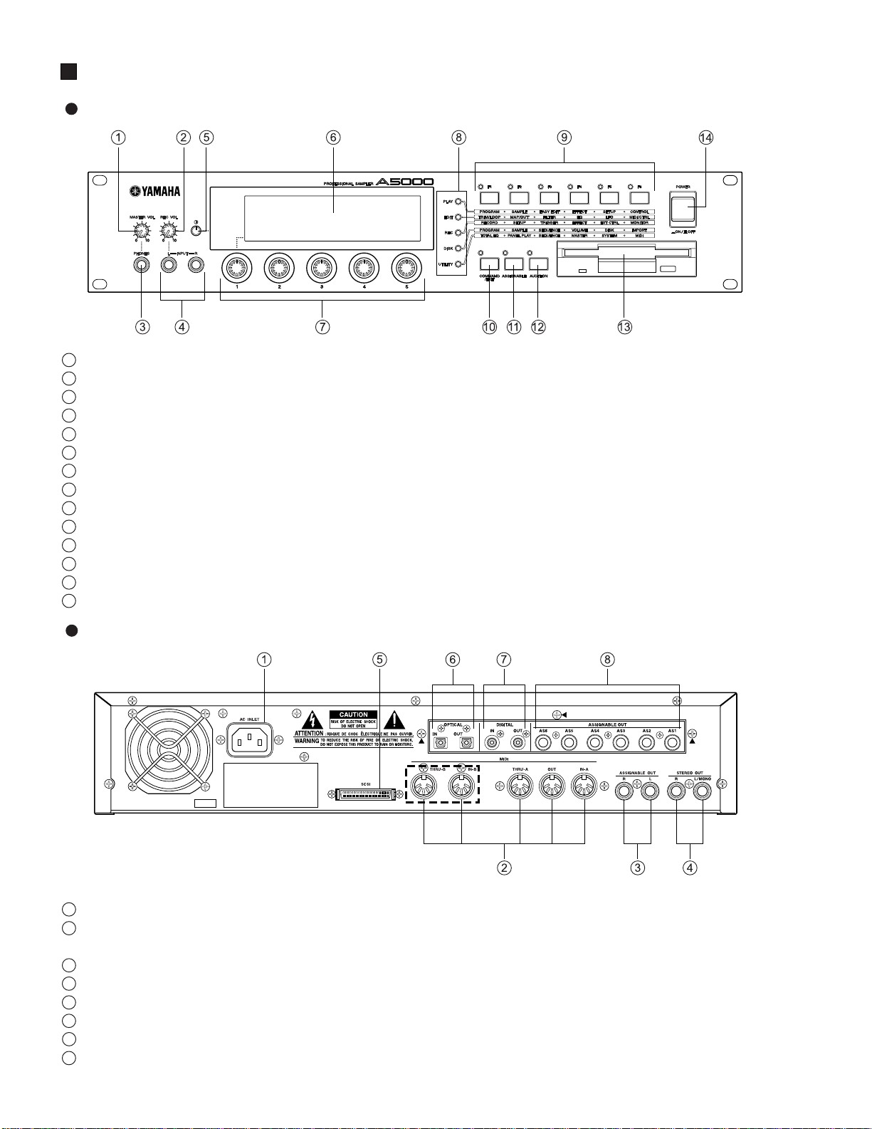
A5000/A4000
PANEL LAYOUT
Front Panel
1 Master Vol [Master Volume]
2 Rec Vol [Recording Volume]
3 Phones jack
4 Input L, Input R jacks
5 LCD Contrast
6 Display
7 Knobs 1-5
8 Mode buttons
9 Function buttons [F1]-[F6]
10
Command Exit button
11
Assignable button
12
Audition button
13
Floppy Disk Drive
14
Power switch
Rear Panel
1 AC inlet
2 Midi In-A, In-B, Out, Thru-A, Thru-B (A5000)
connectors / Midi In, Out, Thru (A4000) connectors
3 Assignable Out L, R jacks
4 Stereo Out L/Mono, R jacks
5 SCSI connector
6 Optical In, Out connectors
7 Digital In, Out connectors
8 Assignable Out jacks 1-6
4
CIRCUIT BOARD LAYOUT
A5000/A4000
5
A5000/A4000
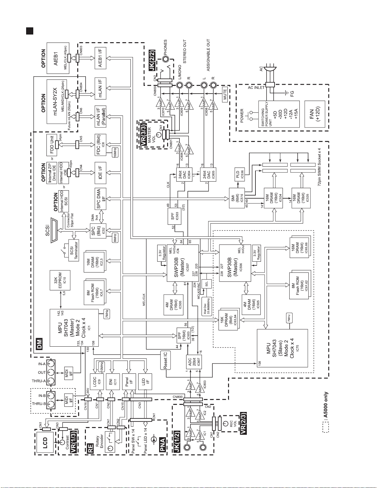
BLOCK DIAGRAM
28CA1-8815099
6
A5000/A4000
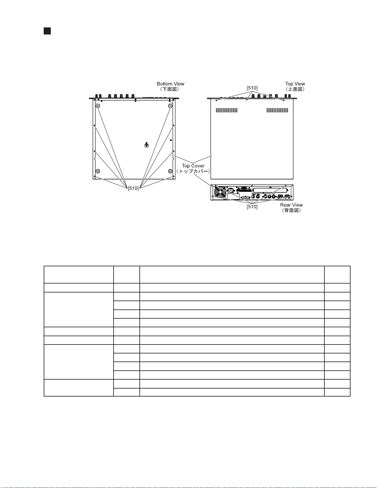
DISASSEMBLY PROCEDURE
1. Top Cover
1-1 Remove the sixteen (16) screws marked [510] and slide the Top Cover to the back side. The top cover can be then
removed.
(Fig.1)
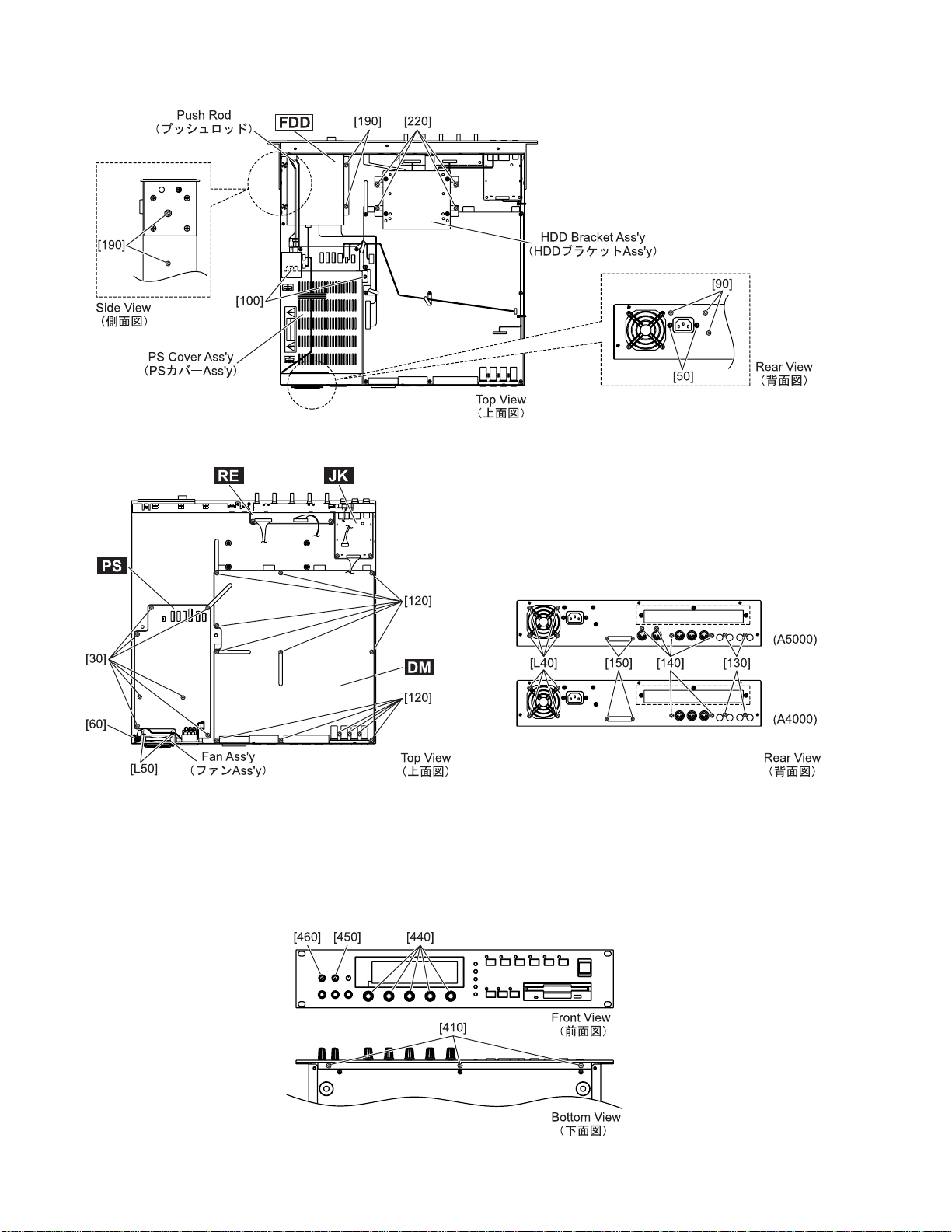
2. Circuit Boards and Unit
After removing the top cover, remove the following screws. Each circuit board can then be removed.
Circuit Boards and Unit Ref.No. Screw Qty
HDD Bracket
1
DM*
FDD Bracket*
PS Cover Ass'y
4
PS*
Fan Ass’y*
3
4
[220]
[120]
[130]
[140]
[150]
[190]
[90]
[100]
[30]
[50]
[60]
[L40]
[L50]
Bind Head Tapping Screw-B 3.0X6 MFZN2Y (EP600130) (fig.2)
Bind Head Tapping Screw-B 3.0X6 MFZN2Y (EP600130) (fig.3)
Bonding Head Screw-B 3.0X10 MFZN2BL (VQ049800)(fig.3)
Bind Head Tapping Screw-P 3.0X8 MFZN2BL (EP630220) (fig.3)
Pan Head Screw 2.5X6 SUS (VV342700)(fig.3)
Bind Head Tapping Screw-B 3.0X6 MFZN2Y (EP600130) (fig.2)
Bonding Head Screw-B 3.0X10 MFZN2BL (VQ049800)(fig.2)
Bind Head Tapping Screw-B 4.0X8 MFZN2BL (EG340190) (fig.2)
Bind Head Tapping Screw-B 3.0X6 MFZN2Y (EP600130) (fig.3)
Bind Head Tapping Screw-P 3.0X8 MFZN2BL (EP630220) (fig.2)
Bind Head Tapping Screw-B 4.0X8 MFZN2BL (EG340190) (fig.3)
Flat Head Screw 3.0X25 MFN133 (V4814 400) (fig.3)
Hexagonal Nut 3.0 MFZN2Y (VA211900) (fig.3)
4
13
2
4(2)*
2
4
3
2
7
2
1
4
4
2
Note: *1 Before removing the DM, remove the HDD Ass'y.
*2 Two for A4000.
*3 Before removing the FDD Ass'y and the PS cover Ass'y, remove the Push Rod.
*4 Before removing the PS and Fan Ass’y, remove the PS cover Ass’y.
7
A5000/A4000
(Fig.2)
(Fig.3)
3. Front Panel
3-1 Remove the knob marked [440], [450], [460].
3-2 Remove the three (3) screws marked [410]. And remove the Front Panel from the Lower Case Assembly.
(Fig.4)
8
4. Circuit Boards and Unit
After removing the front panel, remove the following screws. Each circuit board can then be removed.(Fig.5)
A5000/A4000
Circuit Boards and Unit
JK
RE
VR
PNA
LCD
Ref.No. Screw Qty
[S230]
[L170]
[L170]
[S140]
[S70]
[S110]
Hexagonal Nut 14X2 M12 (ES200210)
Bind Head Tapping-B 3.0X6 MFZN2Y (EP600130)
-
Washer
-
Nut
Bind Head Tapping-B 3.0X6 MFZN2Y (EP600130)
Bind Head Tapping-B 3.0X6 MFZN2Y (EP600130)
Cup Tapping Screw-B 3.0X6 MFZN2Y (V264 4100 )
Bind Head Tapping-B 3.0X6 MFZN2Y (EP600130)
3
2
5
5
2
4
4
4
(Fig.5)
9
A5000/A4000
(
)
(
)
)
(
)
(
)
(
y)
(
)
y
y
(
)
(
)
(
)
(
y)
(
)
(
)
y)
)
)
(
)
(
)
)
)
)
)
(
y)
(
)
(
y)
(
)
(
y)
(
y)
LSI PIN DESCRIPTION
PIN
NAME I/ O FU N C TION
NO.
1Vss
2 CA0 I 122 HMD0 I/O
3 CA1 I 123 HMD1 I/O
4 CA2 I 124 HMD2 I/O
5 CA3 I 125 HMD3 I/O
6 CA4 I 126 HMD4 I/O
7 CA5 I Address bus of internal register 127 HMD5 I/O
8 CA6 I 128 HMD6 I/O Wave memory data bus (Upper 16 bits
9 CA7 I 129 HMD7 I/O
10 CA8 I 130 HMD8 I/O
11 CA9 I 131 HMD9 I/O
12 CA10 I 132 HMD10 I/O
13 CA11 I 133 HMD11 I/O
14 VSS 15 CD0 I/O 135 HMD13 I/O
16 CD1 I/O 136 HMD14 I/O
17 CD2 I/O 137 HMD15 I/O
18 CD3 I/O 138 VSS 19 CD4 I/O 139 H MA0 O
20 CD5 I/O 140 H MA1 O
21 CD6 I/O 141 H MA2 O
22 CD7 I/O 142 H MA3 O
23 CD8 I/O Data bus of internal register 143 HMA4 O
24 CD9 I/O 144 H MA5 O
25 CD10 I/O 145 HMA6 O
26 CD11 I/O 146 HMA7 O
27 CD12 I/O 147 HMA8 O
28 CD13 I/O 148 HMA9 O
29 CD14 I/O 149 HMA10 O
30 VDD - (Power supply) 150 VDD - (Power supply)
31 VSS - (Ground) 151 VSS - (Ground)
32 CD15 I/O 152 HMA11 O
33 CSN I Chip select 153 HMA12 O Wave m emory address bus
34 WRN I Wri te strobe 154 HMA13 O
35 RDN I Read strobe 155 HM A14 O
36 VDD 37 SYSH0 O 157 HMA16 O
38 SYSH1 O 158 HMA17 O
39 SYSH2 O 159 HMA18 O
40 SYSH3 O NSYS/LNSYS upper 16 bits output 160 HMA19 O
41 SYSH4 O 161 HMA20 O
42 SYSH5 O 162 HMA21 O
43 SYSH6 O 163 HMA22 O
44 SYSH7 O 164 HMA23 O
45 KONO0 O 165 HMA24 O
46 KONO1 O Key on data 166 VSS 47 KONO2 O 167 MRASN O
48 KONO3 O 168 MCASN O
49 VSS 50 SYSL0 I/O 170 MW EN O W ave memory wr ite enable
51 SYSL1 I/O 171 VSS 52 SYSL2 I/O 172 LMD0 I/O
53 SYSL3 I/O NSYS input/LNSYS output lower 8 bits 173 LMD1 I/O
54 SYSL4 I/O 174 LMD2 I/O
55 SYSL5 I/O 175 LMD3 I/O
56 SYSL6 I/O 176 LMD4 I/O
57 SYSL7 I/O 177 LMD5 I/O
58 KONI0 I 178 LMD6 I/O
59 KONI1 I Key on data input 179 LMD7 I/O Wave memory data bus (Lower 16 bits)
60 VDD - (Power supply) 180 VDD - (Power supply)
61 VSS - (Ground) 181 VSS - (Ground)
62 KONI2 I 182 LMD8 I/O
63 KONI3 I 183 LMD9 I/O
64 D AC0 O D AC output 184 LMD10 I/O
65 D AC1 O 185 LMD11 I/O
66 WC LK O D A C0 /D A C1 wo rd cl ock 186 LM D1 2 I/ O
67 MELO0 O 187 LMD13 I/O
68 MELO1 O 188 LMD14 I/O
69 MELO2 O 189 LMD15 I/O
70 MELO3 O MEL wave data output 190 VSS 71 MELO4 O 191 LMA0 O
72 MELO5 O 192 LMA1 O
73 MELO6 O 193 LMA2 O
74 MELO7 O 194 LMA3 O
75 VDD 76 AD LR O A D C w o rd c l ock 1 96 L M A5 O
77 MELI0 I 197 LMA6 O
78 MELI1 I 198 LMA7 O
79 MELI2 I 199 LMA8 O
80 MELI3 I MEL wave data i nput 200 LMA9 O
81 MELI4 I 201 LMA10 O
82 MELI5 I 202 LMA11 O
83 MELI6 I 203 VSS 84 MELI7 I 204 LMA12 O
85 VSS 86 RCASN O DRAM column addres s strobe (RAS signal
87 RA8 O 207 LMA15 O
88 RA7 O 208 LMA16 O
89 RA6 O 209 LMA17 O
90 VDD - (Power supply) 210 VDD - (Power supply)
91 VSS - (Ground) 211 VSS - (Ground)
92 RA5 O DRAM address bus 212 LMA18 O
93 RA4 O 213 LMA19 O
94 RA3 O 214 LMA20 O
95 RA2 O 215 LMA21 O
96 RA1 O 216 LMA22 O
97 RA0 O 217 LMA23 O
98 RRASN O DRAM row address strobe (RAS signal
99 RWEN O DARM write enabl e 219 VSS -
100 VSS 101 RD7 I/O 221 SYOD O Sync. signal for HCLK/QCLK
102 RD6 I/O 222 QCLK O 1/12 master clock (64Fs
103 RD5 I/O 223 HCLK O 1/6 master clock (128Fs
104 RD4 I/O 224 CK256 O 1/3 master clock (256Fs
105 RD3 I/O 225 SYSCLK O 1/2 master clock (384Fs
106 RD2 I/O 226 VDD 107 RD1 I/O 227 SYI I Sync. clock
108 RD0 I/O 228 MCLKI I Master c lock input
109 VSS 110 RD17 I/O 230 VDD 111 RD16 I/O DRAM data bus 231 XIN I Crystal osc. input
112 RD15 I/O 232 XOUT O Crystal osc. output
113 RD14 I/O 233 VSS 114 RD13 I/O 234 ICN I Initial clear
115 RD12 I/O 235 CHIP2 I 2 chips mode enable
116 RD11 I/O 236 SLAVE I Master/Slave select when 2 chips mode
117 RD10 I/O 237 TESTON I
118 RD9 I/O 238 ACIN I Test pin
119 RD8 I/O 239 DCTEST I
120 VDD -
Ground
Ground
Power suppl
Ground
Power suppl
Ground
Ground
Ground
Power suppl
PIN
NAME I/ O FU N C TION
NO.
121 VSS -
134 HMD12 I/O
156 HMA15 O
RAS when DRAM(s) is connected to wave memor
169 MOEN O Wave memory output enable
195 LMA4 O
205 LMA13 O W ave memory address bus (Lower data memor
206 LMA14 O
218 LMA24 O
220 SYO O Sync. signal for master clock
229 MCLKO O Master clock output
240 VDD -
CAS when DRAM(s) is connected to wave memor
Ground
Ground
Ground
Ground
Ground
Ground
Ground
Power suppl
Power suppl
Ground
Power suppl
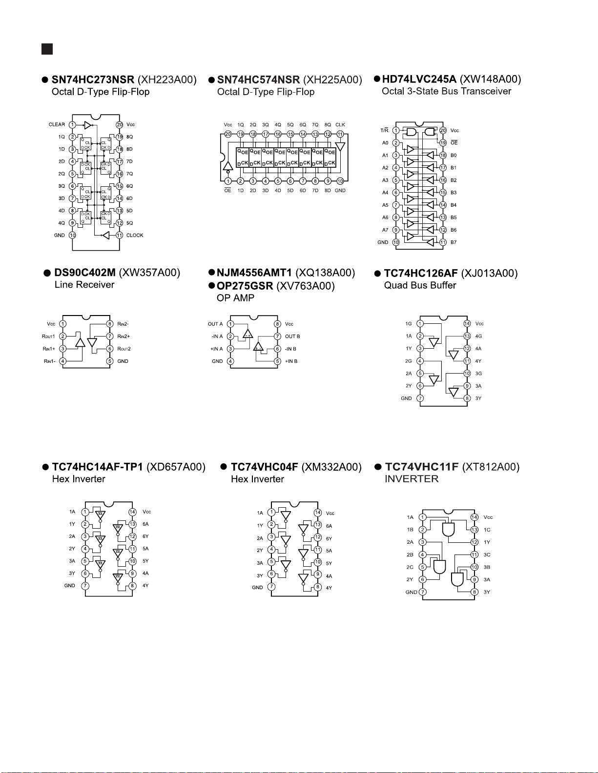
(IC507)TC 20 3C7 60HF - 002 (XS725A 00) SWP 30B (AW M Tone Ge ner at or cop ed wi t h M EG) Sta ndard Wave Pr ocesso r
10

A5000/A4000
D65611GB-039-3B (XS323A00) ENI
PIN
NO.
PIN
NO.
1
CLRN I Clear Status 23
P3 I/O
2
E1A I Rotary Encoder 1 Input A 24
P4 I/O
3
E1B I Rotary Encoder 1 Input B 25
P5 I/O
4
E2A I Rotary Encoder 2 Input A 26
P6 I/O
I/O Po rt
5
E2B I Rotary Encoder 2 Input B 27
P7 I/O
6
E3A I Rotary Encoder 3 Input A 28
D0 I/O
7
E3B I Rotary Encoder 3 Input B 29
D1 I/O
8
E4A I Rotary Encoder 4 Input A 30
GND - Ground
9
E4B I Rotary Encoder 4 Input B 31
D2 I/O
10
E5A I Rotary Encoder 5 Input A 32
D3 I/O
CPU Da ta Bus
11
E5B I Rotary Encoder 5 Input B 33
D4 I/O
12
E6A I Rotary Encoder 6 Input A 34
GND - Ground
13
E6B I Rotary Encoder 6 Input B 35
D5 I/O
14
E7A I Rotary Encoder 7 Input A 36
D6 I/O
CPU Da ta B us
15
E7B I Rotary Encoder 7 Input B 37
D7 I/O
16
VDD - Power Supply 38
GND - Ground
17
GND - Ground 39
VDD - Power Supply
18
E8A I Rotary Encoder 8 Input A 40
A0 I Address Bus
19
E8B I Rotary Encoder 8 Input B 41
A1 I Address Bus
20
P0 I/O
42
WRN I Write Enable
21
P1 I/O
I/O Port 43
RDN I Read Enabl e
22
P2 I/O
44
CSN I Ch ip S ele c t
D65621GF-028-3B9 (XS370A00) SMI
PIN
NO.
PIN
NO.
1 LMA24 I 41
VDD - Power Supply
2 LMA23 I 42 L1RAS2 O R AS2 for LoMem S IMM 1
3 LMA22 I 43 L1RAS3 O R AS3 for LoMem S IMM 1
4 LMA21 I Low Memory Address 44
GND - Ground
5 LMA20 I 45 HDRAS0 O RAS for HiMem DRAM 0
6 LMA19 I 46 HDRAS1 O RAS for HiMem DRAM 1
7 LMA18 I 47
GND - Ground
8 HMA24 I 48
VDD - Power Supply
9 HMA23 I H igh Memory Address 49 LDRAS0 O R AS for LoMem D RAM 0
10 HMA22 I 50 LDRAS1 O R AS for LoMem D RAM 1
11 HMA21 I 51
LMA1 I Low Memor y Address
12
GND - Ground 52
LMA0 I
13 HMA20 I 53
GND - No.53
14 HMA19 I H igh Memory Address 54
LMA1X O Low Memory Address Exchanged
15 HMA18 I 55
LMA0X O
16
RASN I Row Address Strobe 56
GND - Ground
17 H0RAS0 O RAS0 for HiMem SIMM 0 57
VDD - Power Supply
18 H0RAS1 O RAS1 for HiMem SIMM 0 58
HMA1 I High Memory Address
19
GND - Ground 59
HMA0 I
20 H0RAS2 O RAS2 for HiMem SIMM 0 60
HMA1X O High Memory Address Exchanged
21 H0RAS3 O RAS3 for HiMem SIMM 0 61
HMA0X O
22
GND - Ground 62
D0 I Data Input
23
VDD - Power Supply 63
D1 I
24 L0RAS0 O R AS0 for LoMem S IMM 0 64
GND - Ground
25 L0RAS1 O R AS1 for LoMem S IMM 0 65
D2 I
26
GND - Ground 66
D3 I Data Input
27 L0RAS2 O R AS2 for LoMem S IMM 0 67
D4 I
28 L0RAS3 O R AS3 for LoMem S IMM 0 68
D5 I
29
GND - Ground 69
A2 I Address
30
VDD - Power Supply 70
WRN I Write
31 H1RAS0 O RAS0 for HiMem SIMM 1 71
GND - Ground
32 H1RAS1 O RAS1 for HiMem S IMM 1 72
VDD - Power Supply
33
GND - Ground 73
CSN I Chip Select
34
VDD - Power Supply 74
A0 I Address
35 H1RAS2 O RAS2 for HiMem SIMM 1 75
A1 I
36 H1RAS3 O RAS3 for HiMem SIMM 1 76
MCLK I Clock (37MHz)
37
GND - Ground 77
SYI I S ync Clock (48kHz)
38 L1RAS0 O R AS0 for LoMem S IMM 1 78
HBANK O HiM em Bank Select 01/23
39 L1RAS1 O R AS1 for LoMem S IMM 1 79
LBANK O LoMem Bank Select 01/23
40
GND - Ground 80
REFRN O Refresh Timing
(IC516)
NAME I/O FUNCTION
NAME I/O FUNCTION
NAME I/O FUNCTION
NAME I/O FUNCTION
(IC11)
11
A5000/A4000
D65636GF-104-3B9 (XS369A00) SPF
PIN
NO.
NAME I/O FUNCTION
1 ICN I Initial Clear 41 SYNIO I Serial Input0 Sync Clock(48kHz)
2 VDD - Power Supply 42 VDD - Power Supply
3 GND - Ground 43 GND - Ground
4 D0 I/O Data Bus 44 DIN0 I Serial Input0 Data Input(1.6MHz)
5 D1 I/O 45 CK256I1 I Serial Input1 256fs Clock(12.8MHz)
6 GND - Ground 46 BCKI1 I Serial Input1 Bit Clock(3.2MHz)
7 D2 I/O Data Bus 47 SYNI1 I Serial Input1 Sync Clock(48kHz)
8 D3 I/O 48 DIN1 I Serial Input1 Data Input(1.6MHz)
9 GND - Ground 49 DAC256O O 256fs Clock for DAC(12.8MHz)
10 VDD - Power Supply 50 DAC64O O 256fs Clock for DAC(3.2MHz)
11 D4 I/O Data Bus 51 DACWCKO O Wor d Clock for DAC(48kHz )
12 D5 I/O 52 DACDTI I DAC Data Input(1.6MHz)
13 GND - Ground 53 DACDT O O DAC Dat a Outp ut(1.6M Hz)
14 D6 I/O Data Bus 54 VDD - Power Supply
15 D7 I/O 55 GND - Ground
16 A4 I Address 56 MONMELO O Monitor MEL Output(1. 6M Hz)
17 CSN I Chip Select 57 DIT128O O 128fs Clock for DIT(6.4MHz)
18 WRN I Write 58 DITWCKO O Word Clock for DIT(48kHz)
19 RDN I Read 59 MUTEI I Mute Request Input(from CPU)
20 DREQ N O DMA Request 60 MUTENO O Mute Request Output(to DAC&DIT)
21 DACKN I DMA Acknowledge 61 ERRI I PLL Error Input(from DIR)
22 GND - Ground 62 GND - Ground
23 VDD - Power Supply 63 VDD - Power Supply
24 D8 I/O Data Bus 64 ERRI RQN O PLL Erro r IR Q
25 D9 I/O 65 TGRESN O TG Reset Signal
26 GND - Ground 66 P7 I/O
27 D10 I/O Data Bus 67 P6 I/O
28 D11 I/O 68 P5 I/O
29 GND - Ground 69 P4 I/O I/O Port
30 VDD - Power Supply 70 P3 I/O
31 D12 I/O Data Bus 71 P2 I/O
32 D13 I/O 72 P1 I/O
33 GND - Ground 73 P0 I/O
34 D14 I/O Data Bus 74 OCSN I Option Chip Select0
35 D15 I/O 75 ODACKN I Option DMA Acknowledge
36 A1 I 76 ODDIR I Option DMA Direction
37 A2 I Address 77 OBOEN O Option Bus Buffer Output Enable
38 A3 I 78 OBDIR O Option Bus Buffer Direction
39 CK256IO I Serial Input0 256fs Clock(12.8MHz) 79 CSOUTN O Chip Sele c t O ut at A4 = 1, A3=1
40 BCKIO I Serial Input0 Bit Clock(3.2MHz) 80 ASSIGN O Write Pulse O ut at A4= 1, A3=0, WR= 0
PIN
NO.
NAME I/O FUNCTION
(IC11)
PCM1800 (XU770A00) A/D Converter
PIN
NO.
1 VINL I Analog input (L ch.) 13 LRCK I/O
2 VRE F1 Reference 1 decoupling cap. 14 BCK I /O
3 REFCOM Reference decoupling common 15 DOUT O Audio dat a output
4 VREF2 Reference 2 decoupling cap. 16 SYSCK I
5 VINR I Analog input (R ch.) 17 DGND
6 R STB I Reset input active “L” 18 VDD
7 BYPAS I LCF bypass control 19 CINNR
8 FMT0 I Audio dat a format 0 20 CINPR Anti-ali asing filter cap. (+ ) R ch.
9 FMT1 I Audio dat a format 1 21 C INNL
10 MODE0 I Master/ Slave mode selection 0 22 CINPL
11 MODE1 I Master/ Slave mode selection 1 23 VCC
12 FSY NC I/O Frame sync. Input/ output 24 AGND Analog Ground
PIN
NO.
Sampling clock input / output
Bit clock input / output
System clock input
Digital ground
Powe r su p ply +5 V
Anti-aliasing f ilter cap. (-) R ch.
Anti-aliasing f ilter cap. (-) L ch.
Anti-aliasing f ilter cap. (+ ) L ch.
Analog power supply
(IC807)
12
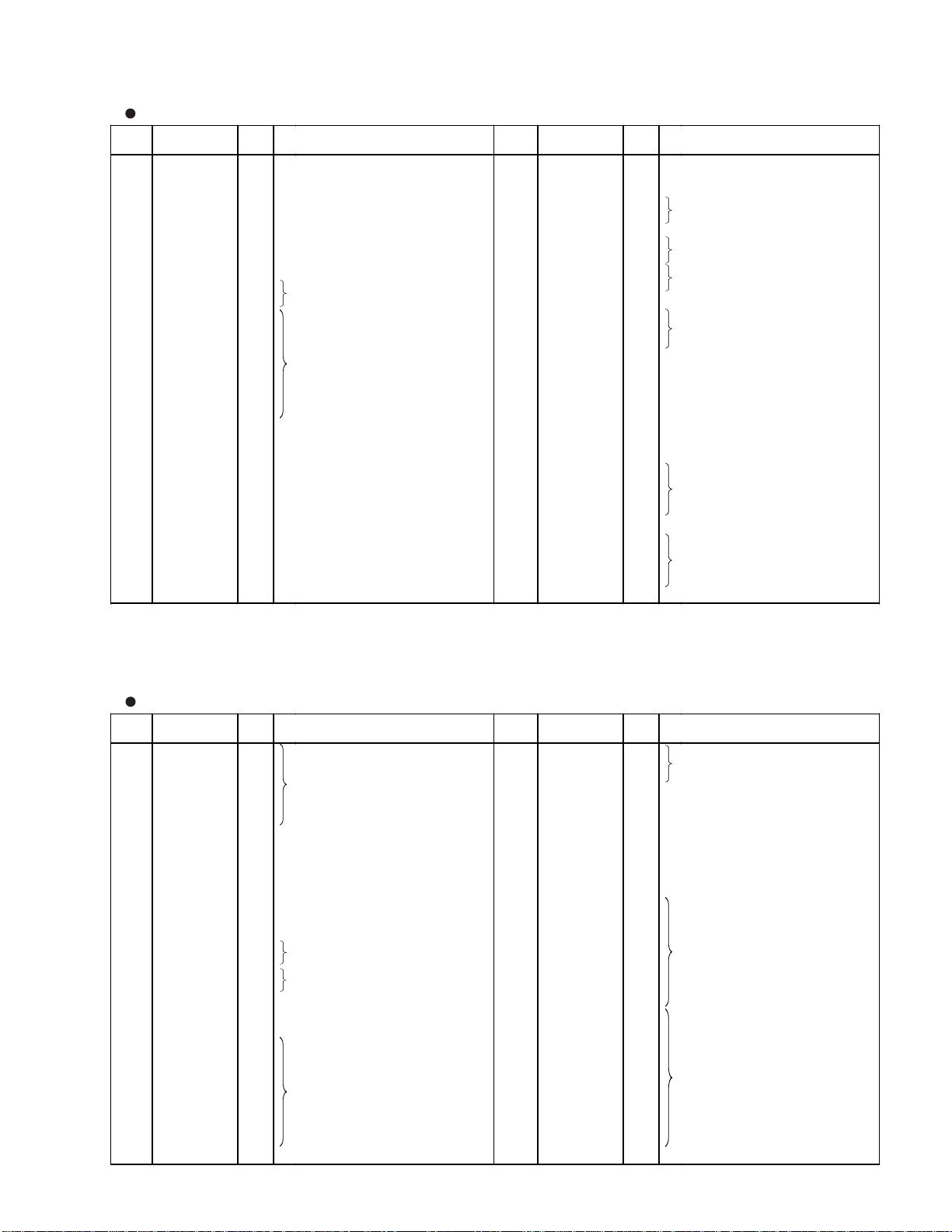
A5000/A4000
SED1335F0B (XQ595A00) LCDC (LCD Controller)
PIN
NO.
NAME I/O
FUNCTION
PIN
NO.
NAME I/O
FUNCTION
1
VA5 O
31
XD2 O
2
VA4 O
32
XD1 O
X driver data bus
3
VA3 O
VRAM address bus 33
XD0 O
4
VA2 O
34
XECL O
X driver enable chain cl ock
5
VA1 O
35
XSCL O
X driver shift clock
6
VA0 O
36
VSS - Ground
7
VR/W O
VRAM writ e strobe 37
LP O
Latch pulse
8
/VCE O
VRAM chip enable 38
WF O
Frame signal
9
NC - 39
YDIS O
LCD power down
10
/RES I Reset 40
YD O
Scan start pulse
11
NC - 41
YSCL O
Scan shift clock
12
NC - 42
VD7 I/O
13
/RD I 80: Read strobe, 68: E clock 43
VD6 I/O
14
/WR I 80: Write stro be, 68: Read/Write
44
VD5 I/O
15
SEL2 I CPU 80/68 bus select 45
VD4 I/O
VRAM data bus
16
SEL1 I 46
VD3 I/O
17
OSC1 I Clock 47
VD2 I/O
18
OSC2 O
48
VD1 I/O
19
/CS I Ch ip select 49
VD0 I/O
20
A0 I Data bus si gnal discrimination 50
VA15 O
21
VDD - Power supply 51
VA14 O
22
D0 I/O
52
VA13 O
23
D1 I/O
53
VA12 O
24
D2 I/O
54
VA11 O
VRAM address bus
25
D3 I/O
55
VA10 O
26
D4 I/O
Data bus 56
VA9 O
27
D5 I/O
57
VA8 O
28
D6 I/O
58
VA7 O
29
D7 I/O
59
VA6 O
30
XD3 O
X driver data bus 60
NC -
HD63266F (XI939A00) FDC (Floppy Disk Controller)
PIN
NO.
NAME I/O
FUNCTION
PIN
NO.
NAME I/O
FUNCTION
1
8"//5" I Data transm is sion speed 33
/TRKO I Track 00 signal
2 XTALSET I Clock select 34 /INDEX I Index signal
3 /RESET I Rest 35 /RDATA I Read data input fr om FDD
4
E//RD I Enable/Read 36
XTAL2 Clock
5 RW//WR I Read/write/Write 37 EXTAL2
6
/CS I Ch ip select 38
NC -
7
/DACK I DMA acknowledge 39
XTAL1 Clock
8
RS0 I Register select 40 EXTAL1
9
RS1 I 41
VSS4 - Ground
10
VSS1 - Ground 42
VSS5 -
11
VSS2 - 43
NC -
12
D0 I/O
44
VCC2 -
13
D1 I/O
45
VCC3 - Power supply
14
D2 I/O
46
VCC4 -
15
D3 I/O
Data bus 47 /WGATE O
Write control
16
D4 I/O
48 /WDATA O
Write data to FDD
17
D5 I/O
49
VSS6 - Ground
18
D6 I/O
50
/STEP O
Step signal to control head of FDD
19
D7 I/O
51
/HDIR O
Direction
20
/DREQ O
DMA request 52 /HLOAD O
Head load
21
/IRQ O
Interrupt request 53
/HSEL O
Head select
22
/DEND I Data end 54
VSS7 - Ground
23
VSS3 - Ground 55
/DS0 O
24 1/2 EX1
56
/DS1 O
Drive select
25
VCC1 - Power supply 57
/DS2 O
26
NUM1 I 58
/DS3 O
27
NUM3 I 59
VSS8 - Ground
28
IFS I Host interface select 60
/MON0 O
29 SFORM I Format data 61
/MON1 O
Motor on
30
/INP I Index pulse 62
/MON2 O
31 /READY I Ready from FDD 63
/MON3 O
32
/WPRT I Write control s ignal 64
VSS9 - Ground
(IC8)
(IC9)
13
A5000/A4000
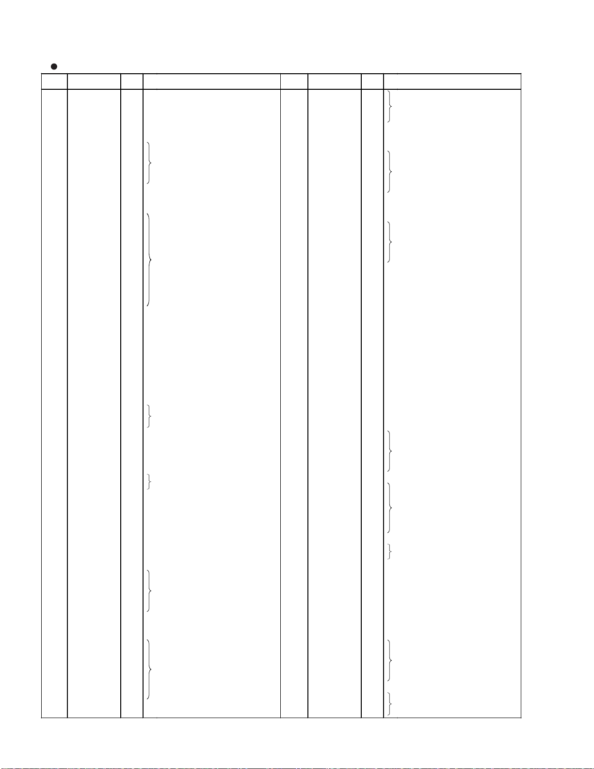
14
HD6437043AE00F
PIN
NO.
NAME I/O FUNCTION
1 / WRHH O HH write 73 D15 I/O
2 DA CK0 O DMA transfer strobe 74 D14 I/O Data bus
3 PA22 O Port A 75 D13 I/O
4 / CASHH O HH Column addres s strobe 76 D12 I /O
5 PE15 I /O Port E 77 VCC I Power supply
6 VSS - Ground 78 D11 I/O Data bus
7 A0 O 79 VSS I Ground
8 A1 O 80 D10 I/O
9 A2 O Address bus 81 D9 I/O
10 A3 O 82 D8 I/O Data bus
11 A4 O 83 D7 I/O
12 VCC - Power supply 84 D6 I/O
13 A5 O Address bus 85 VCC I Power supply
14 VSS - Ground 86 D5 I/O Data bus
15 A6 O 87 VSS - Ground
16 A7 O 88 D4 I/O
17 A8 O 89 D3 I/O
18 A9 O 90 D2 I/O Data bus
19 A10 O 91 D1 I/O
20 A11 O Address bus 92 D0 I/O
21 A12 O 93 VSS - Ground
22 A13 O 94 XTAL I Crystal oscillator
23 A14 O 95 MD3 I Mode select 3
24 A15 O 96 EXTAL I Crystal oscillator
25 A16 O 97 MD2 I Mode select 2
26 VCC - Power supply 98 NMI I N on-maskable interrupt
27 A17 O Address bus 99 VCC I Power supply
28 VSS - Ground 100 PA16 I/O Port A
29 /CASHL O HL Colum n address strobe 101 / WAI T I/O Wait
30 PA19 I/O Port A 102 MD1 I Mode select 1
31 /RAS O Row address strobe 103 MD0 I Mode select 0
32 /CASL O Column address strobe (low) 104 PLLVC C I PLL power supply
33 PA18 I/O Port A 105 PLLCAP I PLL capacitor
34 /CASH O Column address strobe (high) 106 PLLVSS I P LL ground
35 VSS - Ground 107 CK I/O Clock
36 RDWR O DRAM read/write 108 /RES I Reset
37 A18 O 109 /DREQ0 I DMA transfer request
38 A19 O Address bus 110 DRAK0 I/O DMA transfer strobe
39 A20 O 111 /DREQ1 I/O DMA transfer request 1
40 VCC I Power supply 112 VCC I Power supply
41 A21 O Address bus 113 PE3 I/O
42 VSS I Groun d 114 PE4 I/O Port E
43 /RD O Read 115 PE5 I/O
44 /WDTOVF O Watch dog timer overflow 116 PE6 I/O
45 D31 I/O Data bus 117 VSS - Ground
46 D30 I/O 118 PF0 I/O
47 /WRH O High write 119 PF1 I/O
48 /WRL O Low write 120 PF2 I/O Port F
49 /CS1 O Chip se le c t 1 121 PF3 I/O
50 /CS0 O Chip se le c t 0 122 PF4 I/O
51 /IRQ3 I Interrupt request 3 123 PF5 I/O
52 /IRQ2 I Interrupt request 2 124 AVSS I Analog ground
53 /CS3 O Chip se le c t 3 125 PF6 I/O Port F
54 /CS2 O Chip se le c t 2 126 PF7 I/O
55 VSS - Ground 127 AVREF I Analog reference voltage
56 D29 I/O 128 AVCC - Analog power supply
57 D28 I/O 129 VSS - Ground
58 D27 I/ O Data bus 13 0 RxDO I Receiv e d a ta
59 D26 I/O 131 PA1 I/O Part A
60 D25 I/O 132 /IRQ0 I Interrupt request 0
61 VSS - Ground 133 RxD1 I Receive data
62 D24 I/O Data bus 134 TXD1 I/O Transmit data
63 VCC - Power supply 135 VCC - Power supply
64 D23 I/O 136 IRQ1 I/O Interrupt request 1
65 D22 I/O 137 PE7 I/O
66 D21 I/O 138 PE8 I/O Port E
67 D20 I/O Data bus 139 PE9 I/O
68 D19 I/O 140 PE10 I/O
69 D18 I/O 141 VSS - Ground
70 D17 I/O 142 PE11 I/O
71 VSS - Ground 143 PE12 I/O Port E
72 D16 I/O Data bus 144 PE13 I/O
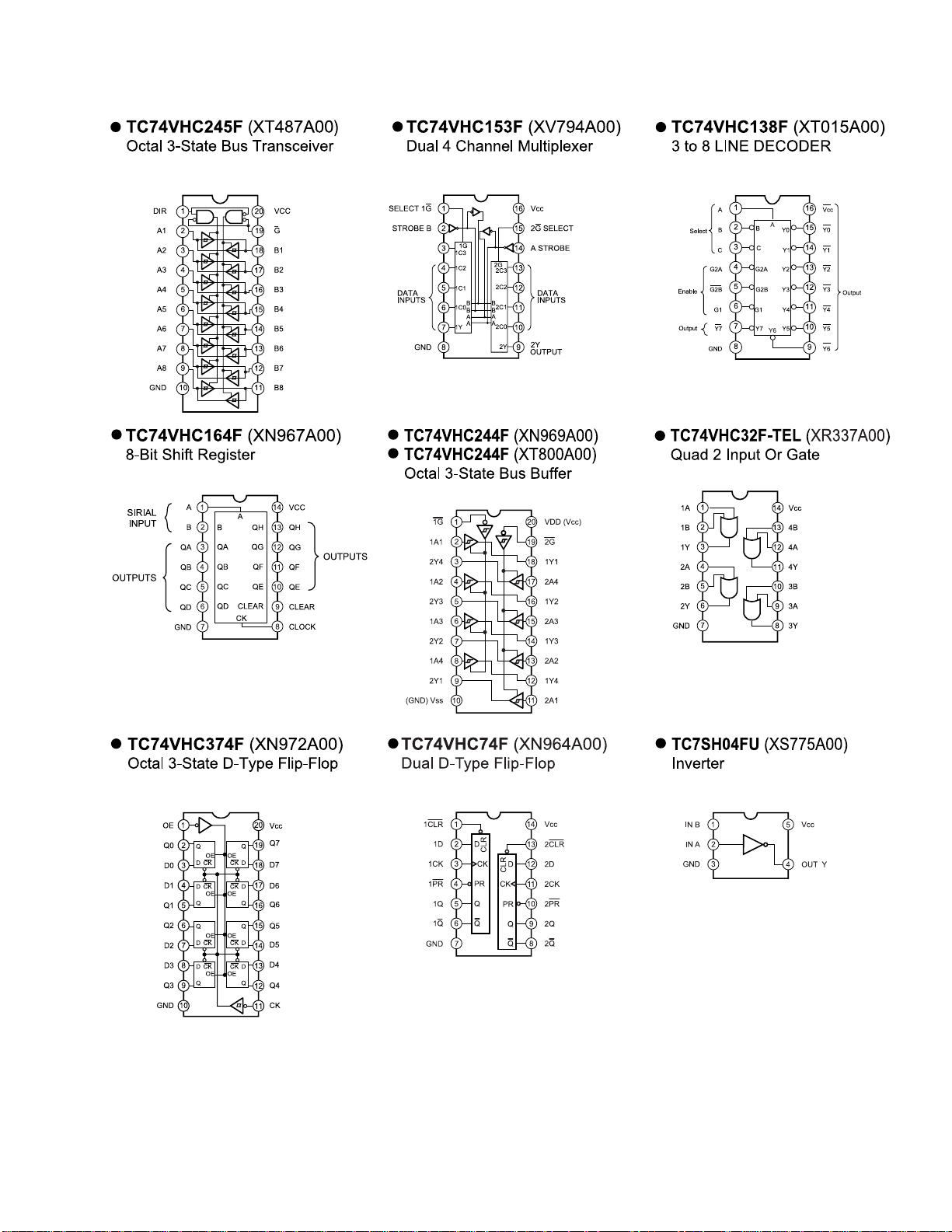
(XW795A00)
CPU
PIN
NO.
NAME I/O FUNCTION
(IC1)

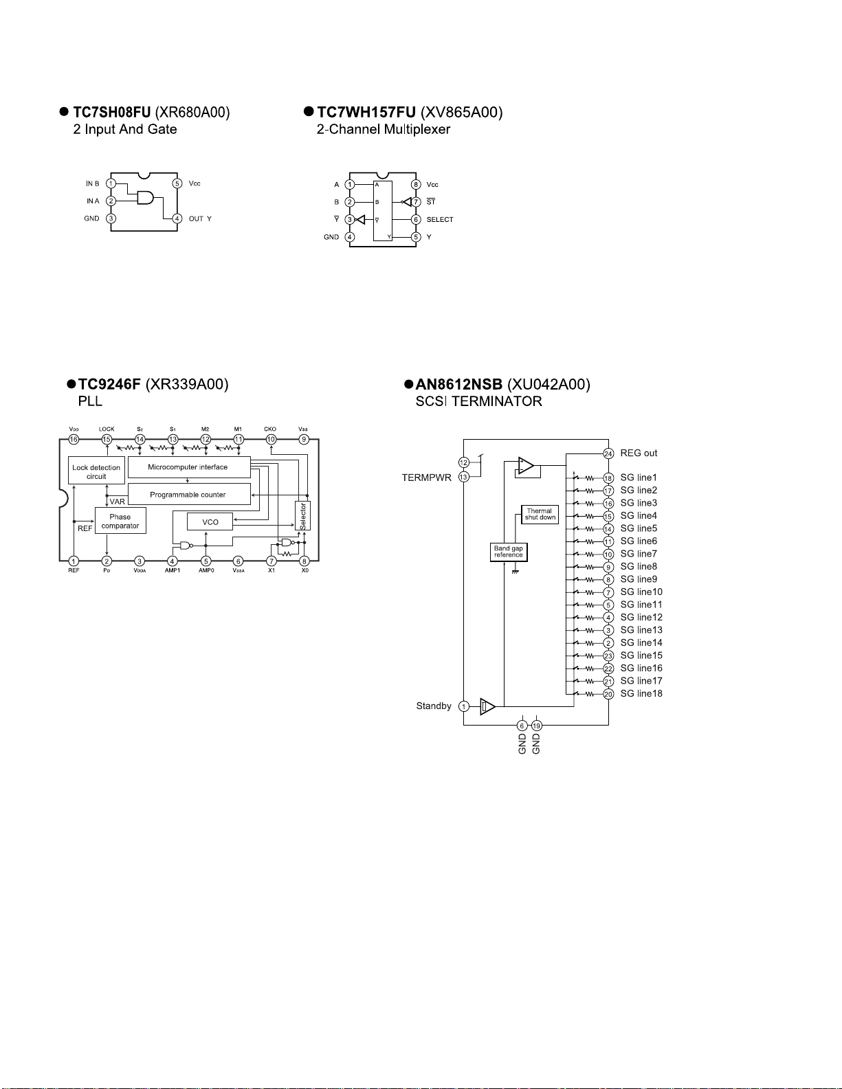
MB87034PF (XK851A00) SPC (SCSI Protocol Controller)
PIN
NO.
NAME I/O
FUNCTION
PIN
NO.
NAME I/O
FUNCTION
1 /RESET I Reset 41
/CLK I Clock
2
VSS - Ground 42
VSS - Ground
3
NC - 43
NC -
4
NC - 44
NC -
5
NC - 45
NC -
6
/DBP I/O
SCSI dat a bus 46
/I/O I/O
Data di recti on
7
VSS - Ground 47
VSS - Ground
8
/DB7 I/O
48
/REQ I/O
Request
9
/DB6 I/O
SCSI dat a bus 49
/C/D I/O
Command/Data
10
/DB5 I/O
50
/SEL I/O
Select
11
VDD - Power supply 51
VDD - Power supply
12
VSS - Ground 52
VSS - Ground
13
VSS - 53
VSS -
14
/DB4 I/O
54
/MSG I/O
Message
15
/DB3 I/O
SCSI dat a bus 55
/RST I/O
Reset
16
/DB2 I/O
56
/ACK I/O
Acknowledge for REQ
17
/DB1 I/O
57
/BSY I/O
Busy
18
VSS - Ground 58
VSS - Ground
19
/DB0 I/O
SCSI dat a bus 59
/ATN I/O
Attenti on condition
20
NC - 60
NC -
21
NC - 61
NC -
22
TEST - 62
INT2 O
Non-m askable interru pt request
23
VSS - Ground 63
VSS - Ground
24 DRESP I Response sig nal for DREQ 64
/CS I Chip sele ct
25
DREQ O
Data transfer request 65
/WT I Write strobe
26
HIN I Output control of HDB0-7,HDBP
66
/WTG I
Data bus write c ontrol (to HDB0-7 ,HDBP)
27
HDB0 I/O
67
/RD I Read strobe
28
HDB1 I/O
68
/RDG I Output co nt ro l for D 0-7,D P
29
HDB2 I/O
Data bus 69
D0 I/O
30
HDB3 I/O
(MB87034 <->data me mo r y) 70
D1 I/O
Data bus
31
HDB4 I/O
71
D2 I/O
(MB87034 <->internal register)
32
HDB5 I/O
72
D3 I/O
33
VDD - Power supply 73
VDD - Power supply
34
HDB6 I/O
74
D4 I/O
35
HDB7 I/O
Data bus 75
D5 I/O
36
HDBP I/O
76
D6 I/O
Data bus
37
A0 I 77
D7 I/O
38
A1 I Resistor select 78
DP I/O
39
A2 I 79
DP0 O
Odd nu mbe r par it y of data bus
40
A3 I 80
INTR O
Int err up t re que s t
PCM1716E (XU829A00) DAC (Digital to Analog Converter)
PIN
NO.
PIN
NO.
1 LRCK I 15
Vcc1 - Analog power supply (+5V)
2 DATA I Data input 16
VOUTL O Lch, analog voltage output
3
BCK I B it clock 17
NC -
4 CLKO O Clock input 18
EXTL O Lch, analog output
5
XTI I Clock input 19 AGND2L - Analog ground
6
XTO O Clock out 20
Vcc2L - Analog power supply (+5V)
7 DGND - Digital ground 21
/ZERO O Zero data flag
8
VDD - D igital power supply (+5V) 22
/RST I Reset
9 Vcc2R - Analog power supply (+5V) 23 /CS/IWO I Chip select
10 AGND2R - Analog ground 24
MODE I Mode control select
(H: Software, L: Hardware)
11
EXTR O Rch, analog output 25
/MUTE I Mute control
12
NC - 26 MD/DM0 I Mode cont rol data/ De-emphasis select 1
13
14
VOUTR
AGND1
O
-
Rch, analog voltage output
Analog ground
27
28
MC/DM1
ML/IIS
I
I
Mode control BCK/ De-emphasis select2
Mode control Latch/ input format select
A5000/A4000
(IC52)
(IC805)
15
A5000/A4000
IC BLOCK DIAGRAM
16
A5000/A4000
17
A5000/A4000
18
TEST PROGRAM
A5000/A4000
TEST No.
00 MIDI OK/NG
01 LCD ALL DOTS ON/OFF
02 LED/SWITCH LIT, OK/NG
03 ENCODER OK/NG
04 CPU (DRAM/EEPROM/DPRAM) OK/NG
05 WAVE MEMORY OK/NG
06 SIM M Displayed CAP ACITY/NG ADDRESS (SIMM)
07 DRIVE 1SECTOR/DMA (SCSI) OK/NG
08 DRIVE 1SECTOR (IDE) OK/NG
09 FD INSERT/VERIFY OK/NG
10 128 (64)TONE/DSPRAM Listning (via DSP RAM)
11 STEREO OUT-L 1 kHz +/- 1 Hz, less than 2.0% distortion, -1 +/- 3 dBm
12 STEREO OUT-R 1 kHz +/- 1 Hz, less than 2.0% distortion, -1 +/- 3 dBm
13 ASSIGNABLE OUT-L 1 kHz +/- 1 Hz, less than 2.5% distortion, -1 +/- 3 dBm
14 ASSIGNABLE OUT-R 1 kHz +/- 1 Hz, less than 2.5% distortion, -1 +/- 3 dBm
15 REC IN (MIC)/SPF 1 kHz +/- 1.5 Hz, less than 3.0% distortion, -1 +/- 4 dBm
16 REC IN (LINE)/SPF 1 kHz +/- 1.5 Hz, less than 2.5% distortion, -1 +/- 4 dBm
17 MUTE Listning
18 ASSIGNABLE OUT-1 1 kHz +/- 1 Hz, less than 0.5% distortion, 0 +/- 3 dBm
19 ASSIGNABLE OUT-2 1 kHz +/- 1 Hz, less than 0.5% distortion, 0 +/- 3 dBm
20 ASSIGNABLE OUT-3 1 kHz +/- 1 Hz, less than 0.5% distortion, 0 +/- 3 dBm
21 ASSIGNABLE OUT-4 1 kHz +/- 1 Hz, less than 0.5% distortion, 0 +/- 3 dBm
22 ASSIGNABLE OUT-5 1 kHz +/- 1 Hz, less than 0.5% distortion, 0 +/- 3 dBm
23 ASSIGNABLE OUT-6 1 kHz +/- 1 Hz, less than 0.5% distortion, 0 +/- 3 dBm
24 DIGITAL & OPTICAL OUT Lintning, measuring
25 DIGITAL IN 1 kHz +/- 5 Hz, less than 0.2% distortion, 17 +/- 4 dBm
26 OPTICAL IN 1 kHz +/- 5 Hz, less than 0.2% distortion, 17 +/- 4 dBm
27 mLAN I/F (26pin)
28 mLAN I/F (50pin)
50 CPU (DRAM/DPRAM) ALL OK/NG
51 WAVE MEMORY ALL Displayed CAPACITY/NG ADDRESS
52 SIMM ALL Displayed CAPACITY/NG ADDRESS
53 DRIVE 100MB VERIFY (SCSI) OK/NG
54 DRIVE 100MB VERIFY (IDE) OK/NG
55 DIGITAL I/O OK/NG
56 OPTICAL I/O OK/NG
90 SCSI TERM POWER Displayed CAPACITY +4.4 ~ 5.1 V
91 SCSI TERM SW Displayed CAPACITY SW ON: 2.85 +/- 0.5 V OFF: 0 +/- 0.5 V
92 REMAIN NOISE less than -70 dBm, PHONES: less than -62 dBm
93 POWER SUPPLY VOL TAGE 5.00 +/- 0.25 V
94 POWER ON MUTE less than 200 mVp-p, PHONES: less than 500 mVp-p
98 FACTORY SET
99 EXIT
TEST TEST RESULTS
19
 Loading...