

Page 1

Virtex UltraScale+ FPGAs
GTM Transceivers
User Guide
UG581 (v1.0) January 4, 2019
Page 2

Revision History
Send Feedback
The following table shows the revision history for this document.
Revision History
Section
01/04/2019 Version 1.0
Initial Xilinx release. N/A
Revision Summary
UG581 (v1.0) January 4, 2019 www.xilinx.com
Virtex UltraScale+ GTM Transceivers 2
Page 3

Table of Contents
Send Feedback
Revision History...............................................................................................................2
Chapter 1: Transceiver and Tool Overview.......................................................5
Introduction to the UltraScale Architecture.............................................................................5
Features........................................................................................................................................6
UltraScale+ FPGAs GTM Transceivers Wizard.......................................................................... 9
Simulation.................................................................................................................................. 10
Implementation.........................................................................................................................11
Chapter 2: Shared Features.....................................................................................12
Reference Clock Input/Output Structure............................................................................... 12
Reference Clock Selection and Distribution...........................................................................14
LCPLL...........................................................................................................................................18
Reset and Initialization............................................................................................................. 23
Power Down...............................................................................................................................45
Loopback.................................................................................................................................... 46
Dynamic Reconfiguration Port................................................................................................ 47
Digital Monitor...........................................................................................................................50
UG581 (v1.0) January 4, 2019 www.xilinx.com
Virtex UltraScale+ GTM Transceivers 3
Chapter 3: Transmitter.............................................................................................. 54
TX Interface................................................................................................................................55
TX FEC......................................................................................................................................... 63
TX Buffer.....................................................................................................................................66
TX Pattern Generator................................................................................................................67
TX Polarity Control.....................................................................................................................71
TX Gray Encoder........................................................................................................................ 71
TX Pre-Coder.............................................................................................................................. 72
TX Fabric Clock Output Control............................................................................................... 73
TX Configurable Driver............................................................................................................. 77
Chapter 4: Receiver......................................................................................................84
RX Analog Front End................................................................................................................. 85
RX Equalizer............................................................................................................................... 87
Page 4

RX CDR........................................................................................................................................ 93
Send Feedback
RX Fabric Clock Output Control............................................................................................... 94
RX Margin Analysis....................................................................................................................98
RX Pre-Coder..............................................................................................................................99
RX Gray Encoder........................................................................................................................99
RX Polarity Control.................................................................................................................. 100
RX Pattern Checker................................................................................................................. 101
RX Buffer...................................................................................................................................104
RX FEC....................................................................................................................................... 106
RX Interface..............................................................................................................................113
Chapter 5: Board Design Guidelines................................................................ 117
Pin Description and Design Guidelines................................................................................ 117
Reference Clock....................................................................................................................... 120
GTM Transceiver Reference Clock Checklist........................................................................ 122
Reference Clock Interface...................................................................................................... 123
AC Coupled Reference Clock..................................................................................................124
Unused Reference Clocks.......................................................................................................125
Reference Clock Output Buffer..............................................................................................125
Reference Clock Power...........................................................................................................125
Power Supply and Filtering.................................................................................................... 125
PCB Design Checklist.............................................................................................................. 129
Appendix A: DRP Address Map of the GTM Transceiver in
UltraScale+ FGPAs.................................................................................................. 133
GTM_DUAL Primitive DRP Address Map...............................................................................133
Appendix B: Additional Resources and Legal Notices........................... 143
Xilinx Resources.......................................................................................................................143
Documentation Navigator and Design Hubs...................................................................... 143
Please Read: Important Legal Notices................................................................................. 144
UG581 (v1.0) January 4, 2019 www.xilinx.com
Virtex UltraScale+ GTM Transceivers 4
Page 5

Chapter 1
Send Feedback
Transceiver and Tool Overview
Introduction to the UltraScale Architecture
The Xilinx® UltraScale™ architecture is the rst ASIC-class architecture to enable mul-hundred
gigabit-per-second levels of system performance with smart processing, while eciently roung
and processing data on-chip. UltraScale architecture-based devices address a vast spectrum of
high-bandwidth, high-ulizaon system requirements by using industry-leading technical
innovaons, including next-generaon roung, ASIC-like clocking, 3D-on-3D ICs, mulprocessor
SoC (MPSoC) technologies, and new power reducon features. The devices share many building
blocks, providing scalability across process nodes and product families to leverage system-level
investment across plaorms.
Virtex® UltraScale+™ devices provide the highest performance and integraon capabilies in a
FinFET node, including both the highest serial I/O and signal processing bandwidth, as well as
the highest on-chip memory density. As the industry's most capable FPGA family, the Virtex
UltraScale+ devices are ideal for applicaons including 1+ Tb/s networking and data center and
fully integrated radar/early-warning systems.
Virtex® UltraScale™ devices provide the greatest performance and integraon at 20 nm,
including serial I/O bandwidth and logic capacity. As the industry's only high-end FPGA at the
20 nm process node, this family is ideal for applicaons including 400G networking, large scale
ASIC prototyping, and emulaon.
Kintex® UltraScale+™ devices provide the best price/performance/wa balance in a FinFET
node, delivering the most cost-eecve soluon for high-end capabilies, including transceiver
and memory interface line rates as well as 100G connecvity cores. Our newest mid-range family
is ideal for both packet processing and DSP-intensive funcons and is well suited for applicaons
including wireless MIMO technology, Nx100G networking, and data center.
UG581 (v1.0) January 4, 2019 www.xilinx.com
Virtex UltraScale+ GTM Transceivers 5
Page 6

Chapter 1: Transceiver and Tool Overview
Send Feedback
Kintex® UltraScale™ devices provide the best price/performance/wa at 20 nm and include the
highest signal processing bandwidth in a mid-range device, next-generaon transceivers, and
low-cost packaging for an opmum blend of capability and cost-eecveness. The family is ideal
for packet processing in 100G networking and data centers applicaons as well as DSP-intensive
processing needed in next-generaon medical imaging, 8k4k video, and heterogeneous wireless
infrastructure.
Zynq® UltraScale+™ MPSoC devices provide 64-bit processor scalability while combining real-
me control with so and hard engines for graphics, video, waveform, and packet processing.
Integrang an ARM®-based system for advanced analycs and on-chip programmable logic for
task acceleraon creates unlimited possibilies for applicaons including 5G Wireless, next
generaon ADAS, and Industrial Internet-of-Things.
This user guide describes the UltraScale architecture GTM transceivers and is part of the
UltraScale architecture documentaon suite available at: www.xilinx.com/ultrascale.
Features
The GTM transceiver in the UltraScale+ FPGA is a high performance transceiver, supporng line
rates between 9.8 Gb/s and 58 Gb/s. Based on the available PLL divider conguraons in the
GTM transceivers, the following line rates are supported:
• PAM4 modulaon:
○ 58 Gb/s – 39.2 Gb/s
○ 29 Gb/s – 19.6 Gb/s
• NRZ modulaon:
○ 29 Gb/s – 19.6 Gb/s
○ 14.5 Gb/s – 9.8 Gb/s
The GTM transceiver is Xilinx’s rst PAM4 enabled transceiver that is highly congurable and
ghtly integrated with the programmable logic resources of the FPGA. The table below
summarizes the features by funconal group that support a wide variety of applicaons.
Table 1: GTM Transceiver Features
UG581 (v1.0) January 4, 2019 www.xilinx.com
Virtex UltraScale+ GTM Transceivers 6
Group Feature
KP4 Reed-Solomon forward error correction (RS-FEC) for up to 2 x 58 Gb/s or 1 x 116 electrical and optical links
PCS
PRBS generator and checker
Programmable FPGA logic interface
Page 7

Chapter 1: Transceiver and Tool Overview
Send Feedback
Table 1: GTM Transceiver Features (cont'd)
Group Feature
LC tank oscillator PLL (LCPLL) for best jitter performance
Flexible clocking with one PLL per Dual (two channels)
Programmable TX output
PMA
Notes:
1. A dual is a cluster or set of two GTM transceiver channels. One GTM_DUAL primitive, one differential reference clock
TX FIR filter with de-emphasis controls
Continuous time linear equalizer (CTLE)
Decision feedback equalization (DFE)
Feed forward equalization (FFE)
pin pair, and analog supply pins. There is no channel primitive.
The GTM transceiver supports NRZ and PAM4
modulaon as well as the following protocols:
• 100GE CAUI2
• 100GE CAUI4
• 200GE CCAUI4
• 400GE (CDAUI8)
• 50GE LAUI
• 50GE LAUI2
• Ethernet AN/LT (auto negoaon/link training)
• OTU4
• Interlaken at 53.125 Gb/s, 25.78125 Gb/s, and 12.5 Gb/s
• CPRI at 48 Gb/s, 24 Gb/s, 12 Gb/s, and 10.1 Gb/s
The rst-me user is recommended to read High-Speed Serial I/O Made Simple, which discusses
high-speed serial transceiver technology and its applicaons. The Xilinx Vivado® IP catalog
includes an UltraScale+ FPGAs GTM Transceivers Wizard to automacally congure GTM
transceivers to support conguraons for dierent protocols and perform custom conguraons.
The GTM transceiver oers a data rate range and features that allow physical layer support for
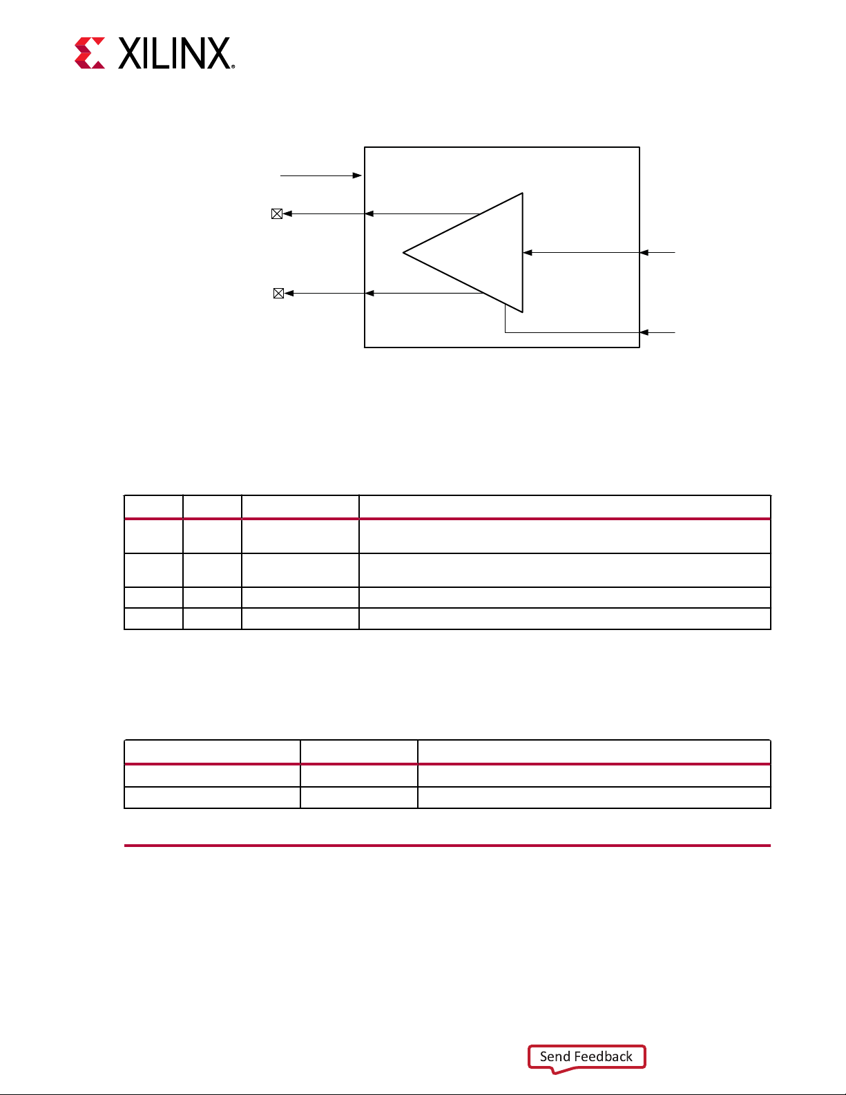
various protocols. The following gure illustrates the clustering of one GTM_DUAL primive.
UG581 (v1.0) January 4, 2019 www.xilinx.com
Virtex UltraScale+ GTM Transceivers 7
Page 8

IBUFDS_GTM /
Send Feedback
OBUFDS_GTM
REFCLK
Distribution
Chapter 1: Transceiver and Tool Overview
Figure 1: GTM Dual Configuration
GTM_DUAL
GTM Channel 0 (CH0)
TX
RX
LCPLL
GTM Channel 1 (CH1)
TX
RX
X20210-061418
The GTM_DUAL primive contains one LCPLL and two GTM channels. Contrary to other
UltraScale+ device transceivers such as the GTH and GTY transceivers, the GTM transceiver
does not contain channel/common primives. All channel ports and aributes are within the
GTM_DUAL primive. The following gure illustrates the topology of a GTM channel.
UG581 (v1.0) January 4, 2019 www.xilinx.com
Virtex UltraScale+ GTM Transceivers 8
Page 9

Driver
Send Feedback
TX
TX
Pre/
Pre2/
Post
Emp
PISO
Pre-Coder
Chapter 1: Transceiver and Tool Overview
Figure 2: GTM Channel Topology
Pattern
Generator
Gray
Encoder
Polarity
FIFO
FEC
TX
Interface
RX PMA
TX PCS
To RX Parallel
Data (Near-End
PCS Loopback)
Pre-
Coder
RX PCS
Gray
Decoder
Polarity
PRBS
Checker
FIFO
FEC
RX EQ SIPOADC
DFE/
FFE
TX PMA
UltraScale+ FPGAs GTM Transceivers Wizard
From RX Parallel
Data (Far-End
PCS Loopback)
RX
Interface
X20211-052918
UG581 (v1.0) January 4, 2019 www.xilinx.com
Virtex UltraScale+ GTM Transceivers 9
The UltraScale+ FPGAs GTM Transceivers Wizard (hereinaer called the Wizard) is the preferred
tool to generate a wrapper to instanate the GTM_DUAL. The Wizard is located in the IP catalog
under the IO Interfaces category.
RECOMMENDED
: Download the most recent IP update before using the Wizard. Details on how to
use this Wizard can be found in the UltraScale+ FPGAs GTM Transceivers Wizard LogiCORE IP Product
Guide (PG315).
Page 10

Chapter 1: Transceiver and Tool Overview
Send Feedback
Simulation
The simulaon environment and the test bench must fulll specic prerequisites before running
simulaon using the GTM_DUAL primives. For instrucons on how to set up the simulaon
environment for supported simulators depending on the used hardware descripon language
(HDL), see the latest version of the UltraScale+ GTM Transceivers Wizard LogiCORE IP Product
Guide (PG315) and Vivado Design Suite User Guide: Logic Simulaon (UG900).
The prerequisites for simulang a design with the GTM_DUAL primives are listed:
• A simulator with support for SecureIP models: SecureIP is an IP encrypon methodology.
SecureIP models are encrypted versions of the Verilog HDL used for implementaon of the
modeled block. To support SecureIP models, a simulator that complies with the encrypon
standards described in the Verilog language reference manual (LRM)—IEEE Standard for
Verilog Hardware Descripon Language (IEEE Std 1364-2005) is required.
• A mixed-language simulator for VHDL simulaon: SecureIP models use a Verilog standard. To
use them in a VHDL design, a mixed-language simulator is required. The simulator must be
able to simulate VHDL and Verilog simultaneously.
• An installed GTM transceiver SecureIP model
• The correct setup of the simulator for SecureIP use (inializaon le, environment variables).
• The correct simulator resoluon (Verilog).
Ports and Attributes
There are no simulaon-only ports on the GTM_DUAL primives. The GTM_DUAL primive has
aributes intended only for simulaon. The following table lists the simulaon-only aributes of
the GTM_DUAL primive. The names of these aributes start with SIM_.
Table 2: GTM_DUAL Simulation-Only Attributes
Attribute Type Description
SIM_RESET_SPEEDUP String If the SIM_RESET_SPEEDUP attribute is set to TRUE (default), an
SIM_DEVICE
String This attribute selects the simulation version to match different
approximated reset sequence is used to speed up the reset time for
simulations, where faster reset times and faster simulation times are
desirable. If the SIM_RESET_SPEEDUP attribute is set to FALSE, the
model emulates hardware reset behavior in detail.
versions of silicon. The default for this attribute is ULTRASCALE_PLUS.
UG581 (v1.0) January 4, 2019 www.xilinx.com
Virtex UltraScale+ GTM Transceivers 10
Page 11

Chapter 1: Transceiver and Tool Overview
Send Feedback
Implementation
It is a common pracce to dene the locaon of GTM transceiver Duals early in the design
process to ensure correct usage of clock resources and to facilitate signal integrity analysis during
board design. The implementaon ow facilitates this pracce through the use of locaon
constraints in the XDC le.
The posion of each GTM transceiver Dual primive is specied by an XY coordinate system that
describes the column number and the relave posion within that column. For a given device/
package combinaon, the transceiver with the coordinates X0Y0 is located at the lowest posion
of the lowest available bank.
There are two ways to create an XDC le for designs that ulize the GTM transceivers. The
preferred method is to use the UltraScale+ FPGAs GTM Transceivers Wizard. The Wizard
automacally generates XDC le templates that congure the transceivers and contain
placeholders for GTM transceiver placement informaon. The XDC les generated by the Wizard
can then be edited to customize operang parameters and placement informaon for the
applicaon.
The second approach is to create the XDC le manually. When using this approach, you must
enter both conguraon aributes that control transceiver operaon as well as the locaon
parameters. Care must be taken to ensure that all of the parameters needed to congure the
GTM transceiver are correctly entered. A GTM_DUAL primive must be instanated as shown in
the following gure.
Figure 3: One-Dual, Two-Channel Configuration (Reference Clock from the LCPLL)
GTM_DUAL
GTM Channel 0 (CH0)
TX
IBUFDS_GTM
LCPLL
GTM Channel 1 (CH1)
RX
TX
RX
X20212-061418
UG581 (v1.0) January 4, 2019 www.xilinx.com
Virtex UltraScale+ GTM Transceivers 11
Each dual contains an LCPLL. Therefore, a reference clock can be connected directly to a
GTM_DUAL primive.
Page 12

Shared Features
Send Feedback
Reference Clock Input/Output Structure
The reference clock structure in the GTM transceiver supports two modes of operaon: input
mode and output mode. In the input mode of operaon, your design provides a clock on the
dedicated reference clock I/O pins that are used to drive the LCPLL. In the output mode of
operaon, the recovered clocks (RXRECCLK0 and RXRECCLK1) from any of the two channels
within the same Dual can be routed to the dedicated reference clock I/O pins. This output clock
can then be used as the reference clock input at a dierent locaon. The mode of operaon
cannot be changed during run me.
Chapter 2: Shared Features
Chapter 2
Input Mode
The reference clock input mode structure is illustrated in the following gure. The input is
terminated internally with 50Ω on each leg to MGTAVCC. The reference clock is instanated in
soware with the IBUFDS_GTM soware primive. The ports and aributes controlling the
reference clock input are ed to the IBUFDS_GTM soware primive.
Figure 4: Reference Clock Input Structure
MGTAVCC
GTREFCLKP
GTREFCLKN
CEB
I
IB
Nominal
50Ω
Nominal
50Ω
+
-
IBUFDS_GTM
MGTAVCC
/2
1'b0
Reserved
To GTREFCLK or
GTM_DUAL
2'b00
2'b01
2'b10
2'b11
To
HROW
O
ODIV2
UG581 (v1.0) January 4, 2019 www.xilinx.com
Virtex UltraScale+ GTM Transceivers 12
REFCLK_HROW_CK_SEL
X20917-061418
Page 13

Chapter 2: Shared Features
Send Feedback
Ports and Attributes
The following table denes the reference clock input ports in the IBUFDS_GTM soware
primive.
Table 3: Reference Clock Input Ports (IBUFDS_GTM)
Port Dir Clock Domain Description
CEB In N/A This is the active-Low asynchronous clock enable signal for the clock buffer.
I In (pad) N/A These are the reference clock input ports that get mapped to GTREFCLKP.
IB In (pad) N/A These are the reference clock input ports that get mapped to GTREFCLKN.
O Out N/A This output drives the GTREFCLK signal in the GTM_DUAL software primitive.
ODIV2 Out N/A This output can be configured to output either the O signal or a divide-by-2
Setting this signal High powers down the clock buffer.
Refer to Reference Clock Selection and Distribution for more details.
version of the O signal. It can drive the BUFG_GT via the HROW routing. Refer
to Reference Clock Selection and Distribution for more details.
The following table denes the aributes in the IBUFDS_GTM soware primive that congure
the reference clock input.
Table 4: Reference Clock Input Attributes (IBUFDS_GTM)
Attribute Type Description
REFCLK_EN_TX_PATH 1-bit Reserved. This attribute must always be set to 1'b0.
REFCLK_HROW_CK_SEL 2-bit Configures the ODIV2 output port:
2'b00: ODIV2 = O.
2'b01: ODIV2 = Divide-by-2 version of O.
2'b10: ODIV2 = 1'b0.
2'b11: ODIV2 = Reserved.
REFCLK_ICNTL_RX
2-bit Reserved. Use the recommended value from the Wizard.
Output Mode
The reference clock output mode can be accessed via the OBUFDS_GTM soware primive. The
reference clock output mode structure for the OBUFDS_GTM primive is shown in the following
gure. The ports and aributes controlling the reference clock output are ed to the
OBUFDS_GTM soware primive.
UG581 (v1.0) January 4, 2019 www.xilinx.com
Virtex UltraScale+ GTM Transceivers 13
Page 14
Chapter 2: Shared Features
Send Feedback
Figure 5: Reference Clock Output Use Model for OBUFDS_GTM
MGTAVCC
GTREFCLKP
GTREFCLKN
O
OB
OBUFDS_GTM
From RXRECCLK0/1
of GTM_DUAL
I
CEB
X20877-061418
Ports and Attributes
The following table denes the ports in the OBUFDS_GTM soware primive.
Table 5: Reference Clock Output Ports (OBUFDS_GTM)
Port Dir Clock Domain Description
CEB In N/A This is the active-Low asynchronous clock enable signal for the clock buffer.
I In (pad) N/A Recovered clock input. Connect to the output port RXRECCLK0/1 of the
O In (pad) N/A Reference clock output port that gets mapped to GTREFCLKP.
OB Out N/A Reference clock output port that gets mapped to GTREFCLKN.
Setting this signal High powers down the clock buffer.
GTM_DUAL primitive.
UG581 (v1.0) January 4, 2019 www.xilinx.com
Virtex UltraScale+ GTM Transceivers 14
The following table denes the aributes in the OBUFDS_GTM soware primive that congure
the reference clock output.
Table 6: Reference Clock Output Attributes (OBUFDS_GTM)
Attribute Type Description
REFCLK_EN_TX_PATH 1-bit Reserved. This attribute must always be set to 1’b1.
REFCLK_ICNTL_TX 5-bit Reserved. Use the recommended value from the Wizard.
Reference Clock Selection and Distribution
The GTM transceivers in Virtex UltraScale+ FPGAs provide dierent reference clock input
opons. Clock selecon and availability is similar to the GTY transceivers in UltraScale+ devices,
but the reference clock selecon architecture supports only one LCPLL shared per Dual (two
GTM transceiver channels).
Page 15

Chapter 2: Shared Features
Send Feedback
From an architecture perspecve, a Dual contains a grouping of two GTM channels inside one
GTM_DUAL primive, one dedicated external reference clock pin pair, and dedicated reference
clock roung. The reference clock for a GTM_DUAL primive must also be instanated. For duals
operang at line rates lower than 16.3725 Gb/s (NRZ) and 32.7 Gb/s (PAM4), the reference clock
for a Dual can also be sourced from the Dual above via GTNORTHREFCLK or from the Dual
below via GTSOUTHREFCLK. For devices that support stacked silicon interconnect (SSI)
technology, the reference clock sharing via the GTNORTHREFCLK and GTSOUTHREFCLK ports
is limited within its own super logic region (SLR). Duals operang at line rates above
16.3725 Gb/s (NRZ) and 32.7 Gb/s (PAM4) should not source a reference clock from another
Dual.
See the UltraScale device data sheets (see hp://www.xilinx.com/documentaon) for more
informaon about SSI technology.
Reference clock features include:
• Clock roung for northbound and southbound clocks.
• Flexible clock inputs available for the LCPLL.
• Stac or dynamic selecon of the reference clock for the LCPLL.
The Dual architecture has two GTM transceivers, one dedicated reference clock pin pair, and
dedicated north and south reference clock roung. Each GTM dual has three clock pair inputs
available:
• One local reference clock pin pair, GTREFCLK.
• One reference clock pin pair for the Dual above, GTSOUTHREFCLK.
• One reference clock pin pair from the Dual below, GTNORTHREFCLK.
The gure below shows the detailed view of a reference clock mulplexer structure within a
single GTM_DUAL primive. The PLLREFCLKSEL port is required when mulple reference clock
sources are connected to this mulplexer. A single reference clock is most commonly used. In the
case of a single reference clock, connect the reference clock to the GTREFCLK ports and e the
PLLREFCLKSEL ports to 3’b001. The Xilinx soware tools handle the complexity of the
mulplexers and associated roung.
UG581 (v1.0) January 4, 2019 www.xilinx.com
Virtex UltraScale+ GTM Transceivers 15
Page 16

Chapter 2: Shared Features
Send Feedback
Figure 6: LCPLL Reference Clock Selection Multiplexer
0
1
2
3
4
5
6
7
GTM_DUAL
LCPLL
LCPLL Output CLK
X20897-061418
PLLREFCLKSEL
GTREFCLK
GTNORTHREFCLK
GTSOUTHREFCLK
GTGREFCLK2PLL
Single External Reference Clock Use Model
Each Dual has one set of dedicated dierenal reference clock input pins (MGTREFCLK[P/N])
that can be connected to the external clock sources. In a single external reference clock use
model, an IBUFDS_GTM must be instanated to use the dedicated dierenal reference clock
source. The following gure shows a single external reference clock connected to the LCPLL
inside the Dual. The user design connects the IBUFDS_GTM output (O) to the GTREFCLK ports
of GTM_DUAL.
Figure 7: Single External Reference Clock in a Dual
IBUFDS_GTM
GTM_DUAL
MGTREFCLKP
MGTREFCLKN
I
O
IB
GTREFCLK
X20898-061418
Note: The IBUFDS_GTM diagram in the above gure is a simplicaon. The output port ODIV2 is le
oang, and the input port CEB is set to logic 0.
The following gure shows a single external reference clock with mulple Duals connected. The
user design connects the IBUFDS_GTM output (O) to the GTREFCLK ports of the GTM_DUAL
primives. In this case, the Xilinx implementaon tools make the necessary adjustments to the
north/south roung as well as the pin swapping necessary to route the reference clock from one
Dual to another when required.
UG581 (v1.0) January 4, 2019 www.xilinx.com
Virtex UltraScale+ GTM Transceivers 16
Page 17

Chapter 2: Shared Features
Send Feedback
Figure 8: Single External Reference Clock with Multiple Duals
D(n+1)
GTM_DUAL
GTREFCLK
D(n)
GTM_DUAL
GTREFCLK
D(n-1)
GTM_DUAL
GTREFCLK
X20215-061418
MGTREFCLKP
MGTREFCLKN
IBUFDS_GTM
I
O
IB
Note: The IBUFDS_GTM diagram in the above gure is a simplicaon. The output port ODIV2 is le
oang, and the input port CEB is set to logic 0.
These rules must be observed when sharing a reference clock to ensure that jier margins for
high-speed designs are met:
• The number of Duals above the sourcing Dual must not exceed one.
• The number of Duals below the sourcing Dual must not exceed one.
• The total number of Duals sourced by an external clock pin pair (MGTREFCLKP/
MGTREFCLKN) must not exceed three Duals.
UG581 (v1.0) January 4, 2019 www.xilinx.com
Virtex UltraScale+ GTM Transceivers 17
The maximum number of Duals that can be sourced by a single clock pin pair is three (six
transceivers). Designs with more than three Duals require the use of mulple external clock pins
to ensure that the rules for controlling jier are followed. When mulple clock pins are used, an
external buer can be used to drive them from the same oscillator.
IMPORTANT
! Upon device conguraon, the clock output from the IBUFDS_GTM which takes inputs
from MGTREFCLKP and MGTREFCLKN can only be used as long as the GTPOWERGOOD signal has
already asserted High.
Ports and Attributes
The following table denes the clocking ports and aributes for the GTM_DUAL primive.
Page 18

Table 7: GTM_DUAL Clocking Ports
Send Feedback
Chapter 2: Shared Features
Port
PLLREFCLKSEL[2:0] In Async Input to dynamically select the input reference clock to the
GTGREFCLK2PLL In Clock Reference clock generated by the internal interconnect logic.
GTREFCLK In Clock External clock driven by IBUFDS_GTM for the LCPLL.
GTNORTHREFCLK In Clock Northbound clock from the Dual below.
GTSOUTHREFCLK In Clock Southbound clock from the Dual above.
PLLREFCLKLOST Out Async A High on this signal indicates that the reference clock to the
PLLREFCLKMONITOR Out Clock LCPLL reference clock selection multiplexer output.
Direct
ion
Clock
Domain
Description
LCPLL. Set this input to 3’b001 and connect to GTREFCLK when
only one clock source is connected to the PLL reference clock
selection multiplexer:
3’b000: Reserved.
3’b001: GTREFCLK selected.
3’b010: Reserved.
3’b011: GTNORTHREFCLK selected.
3’b100: Reserved.
3’b101: GTSOUTHREFCLK.
3’b110: Reserved.
3’b111: GTGREFCLK2PLL.
This input is reserved for internal testing purposes only.
phase frequency detector of the LCPLL is lost.
LCPLL
Each Dual contains one LC-based PLL, referred to as LCPLL, and cannot be shared with
neighboring Duals. The internal clocking architecture of the GTM Dual is shown in the following
gure.
UG581 (v1.0) January 4, 2019 www.xilinx.com
Virtex UltraScale+ GTM Transceivers 18
Page 19

REFCLK Distribution
Send Feedback
Chapter 2: Shared Features
Figure 9: Internal Dual Clocking Architecture
GTM_DUAL
GTM Channel 0 (CH0)
TX PMA
TX PCS
RX PMA
RX PCS
LCPLL
GTM Channel 1 (CH1)
TX PMA
TX PCS
RX PMA
RX PCS
X20900-061418
The LCPLL input clock selecon is described in Reference Clock Selecon and Distribuon. The
LCPLL outputs feed the TX and RX clock divider blocks, which control the generaon of serial
and parallel clocks used by the PMA and PCS blocks. The LCPLL is shared between the TX and
RX datapaths.
The gure below illustrates a conceptual view of the LCPLL architecture. The input clock can be
divided by a factor of M before it is fed into the phase frequency detector. The feedback divider
N determines the voltage-controlled oscillator (VCO) mulplicaon rao. For line rates below
28.1 Gb/s (NRZ) and 56.2 Gb/s (PAM4), a fraconal-N divider is supported where the eecve
rao is a combinaon of the N factor plus a fraconal part. The LCPLL output frequency depends
on the sengs of LCPLLCLKOUT_RATE. When LCPLLCLKOUT_RATE is set to HALF, the output
frequency is half of the VCO frequency. When it is set to FULL, the output frequency is the same
as the VCO frequency. A lock indicator block compares the frequencies of the reference clock
and VCO feedback clock to determine if a frequency lock has been achieved.
UG581 (v1.0) January 4, 2019 www.xilinx.com
Virtex UltraScale+ GTM Transceivers 19
Page 20

PLL
f
PLLClkout
= f
PLLClkin
*
N + FractionalDivider
M*LCPLLCLKOUT _ RATE
f
LineRate
= f
PLLClkout
*Modulation
FractionalDivider = N
SDM
+ 0. < FractionalPart >
FractionalPart
=
SDMDAT A
2
SDMW IDTH
Send Feedback
CLKIN
/M
Figure 10: Internal Dual Clocking Architecture
Lock
Indicator
Phase
Frequency
Detector
Charge
Pump
Loop
Filter
VCO
/2
Chapter 2: Shared Features
PLL
LOCKED
PLL
CLKOUT
/N-Fractional
LCPLLCLKOUT_RATE
The LCPLL VCO operates within 9.8 GHz—14.5 GHz. The Xilinx soware tool chooses the
appropriate LCPLL seng based on applicaon requirements. Equaon 2-1 shows how to
determine the PLL output frequency (GHz).
Equaon 2-2 shows how to determine the line rate (Gb/s).
Equaon 2-3 and Equaon 2-4 show how to determine the fraconal divider presented in
Equaon 2-1.
X20901-052418
The table below lists the allowable values.
Table 8: LCPLL Divider Settings
M LCPLL_REFCLK_DIV 1, 2, 3, 4
N PLLFBDIV[7:0] 16–160 (Integer only)
LCPLLCLKOUT_RATE LCPLLCLKOUT_RATE 1'b1: 1 (Full), 1'b0: 2 (Half)
Modulation See TX Configurable Driver 2 (NRZ), 4 (PAM4)
N
SDM
SDMDATA SDMDATA[SDMWIDTH – 1:0] Fractional part of fractional divider.
SDMWIDTH SDM_WIDTHSEL 16, 20, 24
UG581 (v1.0) January 4, 2019 www.xilinx.com
Virtex UltraScale+ GTM Transceivers 20
Factor Attribute or Port Valid Settings
SDMDATA[SDMWIDTH + 1:SDMWIDTH] Integer part of fractional divider. (Two’s
complement) –2, –1, 0, 1
0 – (224 – 1)
Page 21

Ports and Attributes
Send Feedback
The following tables dene the LCPLL ports and aributes, respecvely.
Table 9: LCPLL Ports
Chapter 2: Shared Features
Port Direction
GTGREFCLK2PLL In Clock Reference clock generated by the internal interconnect
PLLFBCLKLOST Out PLLMONCLK A High on this signal indicates the feedback clock from the
PLLFBDIV[7:0] In Async PLL feedback divider selection. Actual feedback divider value
PLLLOCK Out Async This active-High LCPLL frequency lock signal indicates that
PLLMONCLK In Clock Stable reference clock for the detection of the feedback and
PLLPD
PLLREFCLKLOST Out PLLMONCLK A High on this signal indicates the reference clock to the
PLLREFCLKMONITOR Out Clock PLL reference clock selection multiplexer output.
PLLRESET In Async This port is driven High and then deasserted to start the
PLLRESETBYPASSMODE In Async Reserved. Tied Low.
PLLRESETDONE Out cfg_mclk Status signal that indicates when the PLL reset sequence is
PLLRESETMASK[1:0] In Async Bit 0 enables bit mask for PLL reset. Bit 1 enables bit mask
PLLRSVDIN[15:0] In Reserved Reserved. This port must be set to 0x0000.
PLLRSVDOUT Out Async Reserved.
BGBYPASSB In Async Reserved. This port must be set to 1’b1. Do not modify this
BGMONITORENB In Async Reserved. This port must be set to 1’b1. Do not modify this
BGPDB In Async Reserved. This port must be set to 1’b1. Do not modify this
BGRCALOVRD[4:0] In Async Reserved. This port must be set to 5’b11111. Do not modify
BGRCALOVRDENB In Async Reserved. This port must be set to 1’b1. Do not modify this
In Async An active-High signal powers down the LCPLL.
Clock
Domain
Description
logic. This input is reserved for internal testing purposes.
LCPLL feedback divider to the phase frequency detector of
the LCPLL is lost
is PLLFBDIV + 2. Valid values are from 14–158. (Actual divider
values are 160–160.)
the LCPLL frequency is within a predetermined tolerance.
The transceiver and its clock outputs are not reliable until
this condition is met.
reference clock signals to the LCPLL. The input reference
clock to the LCPLL or any output clock generated from the
LCPLL must not be used to drive this clock. This clock is
required only when using the PLLFBCLKLOST and
PLLREFCLKLOST ports. It does not affect the LCPLL lock
detection, reset, and power-down functions.
phase frequency detector of the LCPLL is lost.
LCPLL reset.
complete.
for PLL SDM reset.
value.
value.
value.
this value.
value.
UG581 (v1.0) January 4, 2019 www.xilinx.com
Virtex UltraScale+ GTM Transceivers 21
Page 22

Table 9: LCPLL Ports (cont'd)
Send Feedback
Chapter 2: Shared Features
Port Direction
RCALEN In Async Reserved. This port must be set to 1’b1. Do not modify this
SDMDATA[25:0] In Async Input to set the Fractional Divider. Bits [SDMWIDTH +
SDMTOGGLE In Async Reserved. Set to 1’b0.
Clock
Domain
Description
value.
1:SDMWIDTH] are the integer part of the divider in two’s
complement. Bits [SDMWIDTH – 1:SDMWIDTH] set the
fractional part of the divider.
Table 10: LCPLL Attributes
Attributes Type Description
BIAS_CFG0 16-bit Reserved. Use the recommended value from the Wizard.
BIAS_CFG1 16-bit Reserved. Use the recommended value from the Wizard.
BIAS_CFG2 16-bit Reserved. Use the recommended value from the Wizard.
BIAS_CFG3 16-bit Reserved. Use the recommended value from the Wizard.
BIAS_CFG4 16-bit Reserved. Use the recommended value from the Wizard.
A_CFG 16-bit Reserved. Use the recommended value from the Wizard.
CRS_CTRL_CFG0 16-bit Reserved. Use the recommended value from the Wizard.
CRS_CTRL_CFG1 16-bit Reserved. Use the recommended value from the Wizard.
DRPEN_CFG 16-bit Reserved. Use the recommended value from the Wizard.
PLL_CFG0 16-bit Reserved. Use the recommended value from the Wizard.
Bit Name Address Description
LCPLLCLKOUT_RATE [8] Sets the LCPLLCLKOUT_RATE factor either to provide full
LCPLL VCO frequency, or half of LCPLL VCO frequency at the
output:
UG581 (v1.0) January 4, 2019 www.xilinx.com
Virtex UltraScale+ GTM Transceivers 22
1'b0: Half rate.
1'b1: Full rate.
PLL_CFG1
Bit Name Address Description
LCPLL_REFCLK_DIV [4:0] LCPLL reference clock divider M settings.
PLL_CFG2
PLL_CFG3 16-bit Reserved. Use the recommended value from the Wizard.
PLL_CFG4 16-bit Reserved. Use the recommended value from the Wizard.
PLL_CFG5 16-bit Reserved. Use the recommended value from the Wizard.
PLL_CFG6 16-bit Reserved. Use the recommended value from the Wizard.
16-bit Reserved. Use the recommended value from the Wizard.
5'b00000: Div by 2.
5'b00001: Div by 3.
5'b00010: Div by 4.
5'b10010: Div by 1.
Other values are not valid.
16-bit Reserved. Use the recommended value from the Wizard.
Page 23

Chapter 2: Shared Features
Send Feedback
Table 10: LCPLL Attributes (cont'd)
Attributes Type Description
SDM_CFG0[15:0] 16-bit Reserved. Use the recommended value from the Wizard.
Bit Name Address Description
SDM_WIDTHSEL [10:9] This attribute sets the denominator of the fractional part of
the feedback divider:
2'b00: 24 bits.
2'b01: 20 bits.
2'b10: 16 bits.
2'b11: Reserved.
SDM_CFG1
SDM_CFG2 16-bit Reserved. Use the recommended value from the Wizard.
SDM_SEED_CFG0 16-bit Reserved. Use the recommended value from the Wizard.
SDM_SEED_CFG1 16-bit Reserved. Use the recommended value from the Wizard.
A_SDM_DATA_CFG0 16-bit Reserved. Use the recommended value from the Wizard.
A_SDM_DATA_CFG1 16-bit Reserved. Use the recommended value from the Wizard.
16-bit Reserved. Use the recommended value from the Wizard.
Reset and Initialization
The GTM transceiver must be inialized aer device power-up and conguraon before it can be
used. The GTM transmier (TX) and receiver (RX) can be inialized independently and in parallel
as shown in the following gure. The GTM transceiver TX and RX inializaon comprises three
steps:
1. Inializing the associated PLL driving TX/RX
2. Inializing the TX and RX datapaths (PMA + PCS)
The TX and RX in the GTM transceiver receive the clock through the LCPLL in the transceiver's
own Dual. In the power-on inializaon sequence, the LCPLL used by the TX and RX must be
inialized rst. The LCPLL used by the TX and RX is reset individually and its reset operaon
independent from TX and RX resets. The TX and RX datapaths must be inialized only aer the
associated LCPLL is locked.
UG581 (v1.0) January 4, 2019 www.xilinx.com
Virtex UltraScale+ GTM Transceivers 23
Page 24

Chapter 2: Shared Features
Send Feedback
Figure 11: GTM Transceiver Initialization Overview
After Configuration
LCPLL Reset
TX Initialization by
GTTXRESET
RX Initialization by
GTRXRESET
RXRESETDONETXRESETDONE
X20903-052818
The GTM transceiver TX and RX use a state machine to control the inializaon process. They
are paroned into a few reset regions. The paron allows the reset state machine to control
the reset process in a sequence that the PMA can be reset rst and the PCS can be reset aer
the asseron of the TXUSERRDY or RXUSERRDY. It also allows the PMA, the PCS, and
funconal blocks inside them to be reset individually when needed during normal operaon.
The GTM transceiver oers two types of reset: inializaon and component.
• Inializaon Reset: This reset is used for complete GTM transceiver inializaon. It must be
used aer device power-up and conguraon. During normal operaon, when necessary,
GTTXRESET and GTRXRESET can also be used to reinialize the GTM transceiver TX and RX.
GTTXRESET is the inializaon reset port for the GTM transceiver TX. GTRXRESET is the
inializaon reset port for the GTM transceiver RX. During inializaon reset,
TXRESETMODE and RXRESETMODE should be set to sequenal mode. All TX PMA, TX PCS,
RX PMA, and RX PCS component resets should be enabled by seng all required component
bits of TXPMARESETMASK, TXPCSRESETMASK, RXPMARESETMASK, and
RXPCSRESETMASK to High.
UG581 (v1.0) January 4, 2019 www.xilinx.com
Virtex UltraScale+ GTM Transceivers 24
• Component Reset: This reset is used for special cases and specic subsecon resets while the
GTM transceiver is in normal operaon. The component that is required to be reset is selected
by seng the associated bit within TXPMARESETMASK, TXPCSRESETMASK,
RXPMARESETMASK, or RXPCSRESETMASK to High. A TX component reset is triggered by
toggling the GTTXRESET port. An RX component reset is triggered by toggling the
GTRXRESET port. Separate component reset ports are available. For the TX, these are
TXCKALRESET, TXFECRESET, TXPCSRESET, and TXPMARESET. For the RX, these are
RXADAPTRESET, RXADCCLKGENRESET, RXBUFRESET, RXCDRFRRESET, RXCDRPHRESET,
RXDFERESET, RXDSPRESET, RXEYESCANRESET, RXFECRESET, RXPCSRESET,
RXPMARESET, and RXPRBSCSCNTRST.
Page 25

Chapter 2: Shared Features
Send Feedback
All reset ports described in this secon iniate the internal reset state machine when driven
High. The internal reset state machines are held in the reset state unl these same reset ports are
driven Low. These resets are all asynchronous. The guideline for the pulse width of these
asynchronous resets is one period of the reference clock, unless otherwise noted.
Note: Do not use reset ports for the purpose of power down. For details on proper power-down usage,
refer to Power Down.
Resetting Multiple Lanes and Quads
Reseng mulple lanes in a Dual or mulple Duals aects the power supply regulaon circuit.
Reset Modes
The GTM transceiver TX and RX resets can operate in two dierent modes: sequenal mode and
single mode.
• Sequenal mode: The reset state machine starts with an inializaon or component reset
input driven High and proceeds through all states aer the requested reset states in the reset
state machine, as shown in Figure 13 for the GTM transceiver TX or Figure 18 for the GTM
transceiver RX unl compleon. The compleon of sequenal mode reset ow is signaled
when (TX/RX)RESETDONE transions from Low to High.
• Single mode: The reset state machine only executes the requested component reset
independently for a predetermined me set by its aribute. It does not process any state aer
the requested state, as shown in Figure 13 for the GTM transceiver TX or Figure 18 for the
GTM transceiver RX. The requested reset can be any component reset to reset the PMA, the
PCS, or funconal blocks inside them. The compleon of a single mode reset is signaled when
(TX/RX)RESETDONE transions from Low to High.
The GTM transceiver inializaon reset must use sequenal mode. All component resets can be
operated in either sequenal mode or single mode. The GTM transceiver uses (TX/
RX)RESETMODE to select between sequenal reset mode and single reset mode. The following
table provides conguraon details that apply to both the GTM transceiver TX and GTM
transceiver RX. Reset modes have no impact on LCPLL reset. During normal operaon, the GTM
transceiver TX or GTM transceiver RX can be reset by applicaons in either sequenal mode or
single mode (GTM transceiver RX only), which provides exibility to reset a poron of the GTM
transceiver. When using either sequenal mode or single mode, (TX/RX)RESETMODE must be
set to the desired value of 50 ns before the asserons of any reset.
UG581 (v1.0) January 4, 2019 www.xilinx.com
Virtex UltraScale+ GTM Transceivers 25
Table 11:
GTM Transceiver Reset Modes Operation
Operation Mode (TX/RX)RESETMODE
Sequential Mode
Single Mode
2'b00
2'b11
Page 26

Table 12: GTM Transceiver Reset Modes Ports
Send Feedback
Port Direction Clock Domain Description
CH[0/1]_RXRESETMODE[1:0] In Async Reset mode port for RX.
2'b00: Sequential mode
(recommended).
2'b01: Reserved.
2'b10: Reserved.
2'b11: Single mode.
Chapter 2: Shared Features
CH[0/1]_TXRESETMODE[1:0]
In Async Reset mode port for TX.
2'b00: Sequential mode
(recommended).
2'b01: Reserved.
2'b10: Reserved.
2'b11: Single mode.
LCPLL Reset
The LCPLL must be reset before it can be used. Each GTM transceiver dual has dedicated reset
ports for its LCPLL. As shown in the gure, PLLRESET is an input that resets LCPLL. PLLLOCK is
an output that indicates the reset process is done. The guideline for this asynchronous PLLRESET
pulse width is one period of the reference clock. Aer a PLLRESET pulse, the internal reset
controller generates an internal LCPLL reset followed by an internal SDM reset. The me
required for LCPLL to lock is aected by a few factors, such as bandwidth seng and clock
frequency.
Figure 12: LCPLL Reset Timing Diagram
UG581 (v1.0) January 4, 2019 www.xilinx.com
Virtex UltraScale+ GTM Transceivers 26
Table 13: LCPLL Reset Ports
Port Dir
PLLRESET In Async Active-High signal that resets the LCPLL.
PLLRESETMASK[1:0] In Async Reserved. Tied to 2’b11.
PLLRESETBYPASSMODE In Async Reserved. Tied Low.
PLLLOCK Out Async Active-High LCPLL frequency lock signal indicates that the
Clock
Domain
Description
LCPLL frequency is within a predetermined tolerance. The
GTM transceiver and its clock outputs are not reliable until
this condition is met.
Page 27

Chapter 2: Shared Features
Send Feedback
TX Initialization and Reset
The GTM transceiver TX uses a reset state machine to control the reset process. The GTM
transceiver TX is paroned into two reset regions, TX PMA and TX PCS. The paron allows TX
inializaon and reset to be operated only in sequenal mode, as shown in the gure below.
The inializing TX must use GTTXRESET in sequenal mode. Acvang the GTTXRESET input
can automacally trigger a full asynchronous TX reset. The reset state machine executes the
reset sequence, as shown in the gure below, covering the whole TX PMA and TX PCS. During
normal operaon, when needed, sequenal mode allows you to reset the TX from acvang
TXPMARESET and connue the reset state machine unl TXRESETDONE transions from Low
to High.
The TX reset state machine does not reset the PCS unl TXUSERRDY is detected High. Drive
TXUSERRDY High aer all clocks used by the applicaon including TXUSRCLK are shown as
stable.
Figure 13: GTM Transceiver TX Reset State Machine Sequence
GTTXRESET
High
Wait until
GTTXRESET from
High to Low
TXPMARESETMASK[0]
= 1?
No
TXPMARESETMASK[1]
= 1?
No
Wait for TXUSERRDY
= 1
Yes
Yes
TX CKCAL Reset
TX PMA Top Reset
TXPCSRESETMASK[0]
= 1?
No
TXPCSRESETMASK[1]
= 1?
No
TXRESETDONE High
Yes
Yes
TX FEC Reset
TX PCS Top Reset
UG581 (v1.0) January 4, 2019 www.xilinx.com
Virtex UltraScale+ GTM Transceivers 27
X20905-060518
Page 28

Ports and Attributes
Send Feedback
The table below lists ports required by the TX inializaon process.
Table 14: TX Initialization and Reset Ports
Chapter 2: Shared Features
Port Dir
CH[0/1]_GTTXRESET In Async This port is driven High and then deasserted to start a TX reset
CH[0/1]_TXRESETMODE[1:0]
CH[0/1]_TXPMARESETMASK[1:0]
CH[0/1]_TXPCSRESETMASK[1:0] In Async TX PCS reset mask selection
CH[0/1]_TXUSERRDY In Async This port is driven High by the user application when TXUSRCLK
CH[0/1]_TXPMARESETDONE Out Async This active-High signal indicates TX PMA reset is complete.
CH[0/1]_TXRESETDONE Out TXUSRCLK This active-High signal indicates the GTM transceiver TX has
CH[0/1]_ TXCKALRESET In Async This port is driven High and then deasserted to start a single
CH[0/1]_ TXPMARESET In Async This port is driven High and then deasserted to start a single
CH[0/1]_ TXFECRESET In Async This port is driven High and then deasserted to start a single
CH[0/1]_ TXPCSRESET In Async This port is driven High and then deasserted to start a single
In Async Reset mode port for TX:
In Async TX PMA reset mask selection:
Clock
Domain
Description
sequence. The components to be reset are determined by
TXPMARESETMASK and TXPCSRESETMASK. In sequential mode,
the resets are performed sequentially. In single mode, the
resets are performed simultaneously.
2’b00: Sequential mode (recommended).
2’b01: Reserved.
2’b10: Reserved.
2’b11: Single mode.
Bit 1: TX PMA.
Bit 0: CKCAL.
Bit 1: TX PCS.
Bit 0: TX FEC.
is stable.
finished reset and is ready for use. This port is driven Low when
GTTXRESET goes High and is not driven High until the GTM
transceiver has completed all TX reset steps.
mode reset on TX CKCAL. The reset is not dependent on
TXRESETMODE or TXPMARESETMASK setting.
mode reset on TX PMA. The reset is not dependent on
TXRESETMODE or TXPMARESETMASK setting.
mode reset on TX FEC. The reset is not dependent on
TXRESETMODE or TXPCSRESETMASK setting.
mode reset on TX PCS. The reset is not dependent on
TXRESETMODE or TXPCSRESETMASK setting.
UG581 (v1.0) January 4, 2019 www.xilinx.com
Virtex UltraScale+ GTM Transceivers 28
Page 29

Chapter 2: Shared Features
Send Feedback
The following table lists aributes required by GTM transceiver TX inializaon. In general cases,
the reset me required by the TX PMA or the TX PCS varies depending on line rate. The factors
aecng PMA reset me and PCS reset me are the user-congurable aributes
TX_PMA_RESET_TIME, TX_PCS_RESET_TIME, TX_CKCAL_RESET_TIME, and
TX_FEC_RESET_TIME.
Table 15: TX Initialization and Reset Attributes
Attribute Type Description
CH[0/1]_RST_TIME_CFG0 16-bit Reserved.
Bit Name Address Description
TX_PCS_RESET_TIME [14:10] Represents the time duration to apply a TX PCS reset. Use
TX_PMA_RESET_TIME [9:5] Represents the time duration to apply a TX PMA reset. Use
TX_CKCAL_RESET_TIME [4:0] Represents the time duration to apply a TX CLKGEN reset.
CH[0/1]_RST_TIME_CFG1 16-bit Reserved.
Bit Name Address Description
TX_FEC_RESET_TIME [4:0] Represents the time duration to apply a TX CKCAL reset.
CH[0/1]_RST_LP_CFG0 16-bit Reserved.
Bit Name Address Description
TX_PCS_RESET_LOOP_ID [11:8] Reserved. Use the recommended value from the Wizard.
TX_PMA_RESET_LOOP_ID [7:4] Reserved. Use the recommended value from the Wizard.
TX_CKCAL_RESET_LOOP_ID [3:0] Reserved. Use the recommended value from the Wizard.
TX_FEC_RESET_LOOP_ID [15:12] Reserved. Use the recommended value from the Wizard.
CH[0/1]_RST_LP_ID_CFG1 16-bit Reserved.
Bit Name Address Description
TX_PCS_LOOPER_END_ID [15:12] Reserved. Use the recommended value from the Wizard.
TX_PCS_LOOPER_START_ID [11:8] Reserved. Use the recommended value from the Wizard.
TX_PMA_LOOPER_END_ID [7:4] Reserved. Use the recommended value from the Wizard.
TX_PMA_LOOPER_START_ID [3:0] Reserved. Use the recommended value from the Wizard.
CH[0/1]_RST_LP_CFG4 1-bit Reserved.
Bit Name Address Description
BYP_HDSHK_TX_PCS_RESET_LOOP [3] Reserved. Use the recommended value from the Wizard.
BYP_HDSHK_TX_CKCAL_RESET_LOOP [0] Reserved. Use the recommended value from the Wizard.
the recommended value from the Wizard. Must be a nonzero value when TXPCSRESETMASK[1] is High and
GTTXRESET initiates the reset process.
the recommended value from the Wizard. Must be a nonzero value when TXPMARESETMASK[1] is High and
GTTXRESET initiates the reset process.
Use the recommended value from the Wizard. Must be a
non-zero value when TXPMARESETMASK[0] is High and
GTTXRESET initiates the reset process.
Use the recommended value from the Wizard. Must be a
non-zero value when TXPMARESETMASK[0] is High and
GTTXRESET initiates the reset process.
UG581 (v1.0) January 4, 2019 www.xilinx.com
Virtex UltraScale+ GTM Transceivers 29
Page 30

Chapter 2: Shared Features
Send Feedback
GTM Transceiver TX Reset in Response to Completion of Configuration
The TX reset sequence shown in TX Inializaon and Reset is not automacally started to follow
global GSR. It must meet these condions:
1. TXRESETMODE must be set to sequenal mode.
2. GTTXRESET must be used.
3. All TXPMARESETMASK and TXPCSRESETMASK bits should be set to High.
4. GTTXRESET cannot be driven Low unl the associated PLL is locked.
5. Ensure that GTPOWERGOOD is High before releasing PLLRESET and GTTXRESET.
If the reset mode is defaulted to single mode, then you must:
1. Wait another 300–500 ns.
2. Assert PLLRESET and GTTXRESET following the reset sequence described in the following
gure.
RECOMMENDED: Use the associated PLLLOCK from the PLL to release GTTXRESET from High to
Low as shown in the gure. The TX reset state machine waits when GTTXRESET is detected High and
starts the reset sequence unl GTTXRESET is released Low.
Figure 14: GTM Transmitter Initialization after Configuration
GTM Transceiver TX Reset in Response to GTTXRESET Pulse in Full Sequential Reset
The GTM transceiver allows you to reset the enre TX completely at any me by sending
GTTXRESET an acve-High pulse. These condions must be met when using GTTXRESET:
UG581 (v1.0) January 4, 2019 www.xilinx.com
Virtex UltraScale+ GTM Transceivers 30
1. TXRESETMODE must be set to sequenal mode.
2. All TXPMARESETMASK and TXPCSRESETMASK bits should be held High during the reset
sequence before TXRESETDONE is detected High.
Page 31

Chapter 2: Shared Features
Send Feedback
3. The associated PLL must indicate locked.
4. The guideline for this asynchronous GTTXRESET pulse width is one period of the reference
clock.
Figure 15: GTM Transmitter Reset after GTTXRESET Pulse in Full Sequential Reset
GTM Transceiver TX Component Reset
TX PMA and TX PCS can be reset individually. Component reset is enabled by seng the
appropriate TXPMARESETMASK and TXPCSRESETMASK bits along with TXRESETMODE and
then toggling GTTXRESET.
Driving GTTXRESET from High to Low starts the component reset process. All
TXPMARESETMASK and TXPCSRESETMASK bits along with TXRESETMODE must be held
constant during the reset process.
When TXRESETMODE is set to sequenal mode, the internal resets are toggled in sequence
depending on TXPMARESTMASK and TXPCSRESETMASK selecon. When TXRESETMODE is
set to single mode, the internal resets are toggled simultaneously depending on
TXPMARESETMASK and TXPCSRESTMASK selecon.
In sequenal mode, if the TX PCS is to be reset, TXUSERRDY must toggle to High prior to the
internal PCS reset signal being released allowing TX reset to be completed.
Direct single-reset ports TXPMARESET, TXCKALRESET, TXPCSRESET, and TXFECRESET are
available to perform single resets of the respecve TX components. When direct single-reset
ports are toggled, a single reset is performed regardless of TXPMARESETMASK,
TXPCSRESETMASK, and TXRESETMODE selecon. These ports must be held Low during any
sequenal or single resets driven by GTTXRESET.
UG581 (v1.0) January 4, 2019 www.xilinx.com
Virtex UltraScale+ GTM Transceivers 31
Page 32

Chapter 2: Shared Features
Send Feedback
Figure 16: GTM Transmitter Reset after GTTXRESET Pulse in Component Sequential
Mode
Figure 17: GTM Transmitter Reset after GTTXRESET Pulse in Component Single Mode
The following table lists the recommended resets for common situaons.
Table 16: Recommended Transmitter Resets for Common Situations
Situation
After power up and
configuration
After turning on a
reference clock to the
PLL being used
After changing the
reference clock to the
PLL being used
After assertion/
deassertion of PLLPD for
the PLL being used
Components to
be Reset
PLL, Entire TX
PLL, Entire TX
PLL, Entire TX
PLL, Entire TX
TXRESETMODE TXPMARESETMASK TXPCSRESETMASK
2'b00 2’b11 2’b11
2'b00 2’b11 2’b11
2'b00 2’b11 2’b11
2'b00 2’b11 2’b11
Recommended TX Reset Setting
1
UG581 (v1.0) January 4, 2019 www.xilinx.com
Virtex UltraScale+ GTM Transceivers 32
Page 33

Chapter 2: Shared Features
Send Feedback
Table 16: Recommended Transmitter Resets for Common Situations (cont'd)
Situation
After assertion/
deassertion of TXPD
TX rate change TX PMA and TX PCS
TX parallel clock source
reset
Notes:
1. TXPCSRESETMASK[0] can be set to 0 if the FEC is bypassed.
Components to
be Reset
Entire TX
TX PCS 2'b00/2'b11
TXRESETMODE TXPMARESETMASK TXPCSRESETMASK
2'b00 2’b11 2’b11
2'b00 2’b11 2’b11
Recommended TX Reset Setting
2’b00 2’b11
After Power-up and Configuration
The PLL being used and the enre GTM TX require a reset aer conguraon. See GTM
Transceiver TX Reset in Response to Compleon of Conguraon.
After Turning on a Reference Clock to the LCPLL/ RPLL Being Used
If the reference clock(s) changes or the GTM transceiver(s) are powered up aer conguraon,
perform a full TX sequenal reset aer the PLL fully completes its reset procedure.
1
After Changing the Reference Clock to the PLL being Used
Whenever the reference clock input to the PLL is changed, the PLL must be reset aerwards to
ensure that it locks to the new frequency. Perform a full TX sequenal reset aer the PLL fully
completes its reset procedure.
After Assertion/Deassertion of PLLPD for the PLL being Used
When the PLL being used goes back to normal operaon aer power down, the PLL must be
reset. Perform a full TX sequenal reset aer the PLL fully completes its reset procedure.
After Assertion/Deassertion of TXPD[1:0]
Aer the TXPD signal is deasserted, perform a full TX sequenal reset.
UG581 (v1.0) January 4, 2019 www.xilinx.com
Virtex UltraScale+ GTM Transceivers 33
Page 34

Chapter 2: Shared Features
Send Feedback
TX Rate Change
When a rate change is performed, a full TX sequenal reset is required aer the rate aributes
have been updated.
TX Parallel Clock Source Reset
The clocks driving TXUSRCLK must be stable for correct operaon. Perform a TX PCS reset aer
the clock source re-locks.
RX Initialization and Reset
The GTM transceiver RX uses a reset state machine to control the reset process. Due to its
complexity, the GTM transceiver RX is paroned into more reset regions than the GTM
transceiver TX. The paron allows RX inializaon and reset to be operated in either sequenal
mode, as shown in the following gure, or single mode:
1. RX in Sequenal Mode: To inialize the GTM transceiver RX, RXRESETMODE must be set to
sequenal mode. The RX components that are required to be rest are determined by seng
the appropriate RXPMARESETMASK and RXPCSRESETMASK bits to High. The reset
sequence is then triggered by toggling GTRXRESET and then internal component resets are
triggered sequenally. The reset state machine executes the reset sequence as shown in the
following gure, covering the enre RX PMA and RX PCS. During normal operaon, the reset
state machine runs unl RXRESETDONE transions from Low to High.
2. RX in Single Mode: When the GTM transceiver RX is in single mode, RXRESETMODE must
be set to single mode. The RX components that are required to be rest are determined by
seng the appropriate RXPMARESETMASK and RXPCSRESETMASK bits to High. The reset
sequence is then triggered by toggling GTRXRESET and the internal component resets are
triggered simultaneously. In addion, RXADAPTRESET, RXADCCLKGENRESET,
RXBUFRESET, RXCDRFRRESET, RXCDRPHRESET, RXDFERESET, RXDSPRESET,
RXEYESCANRESET, RXFECRESET, RXPCSRESET, RXPMARESET and RXPRBSCNTRESET
pins are available to reset those components directly in single mode.
In either sequenal mode or single mode, the RX reset state machine does not reset the PCS
unl RXUSERRDY goes High. Drive RXUSERRDY High aer all clocks used by the applicaon,
including RXUSRCLK, are shown to be stable.
UG581 (v1.0) January 4, 2019 www.xilinx.com
Virtex UltraScale+ GTM Transceivers 34
Page 35

GTRXRESET
Send Feedback
High
Wait until
GTRXRESET from
High to Low
Chapter 2: Shared Features
Figure 18: GTM Transceiver RX Reset State Machine Sequence
RXPMARESETMASK[0]
= 1?
No
RXPMARESETMASK[1]
= 1?
No
RXPMARESETMASK[2]
= 1?
No
RXPMARESETMASK[3]
= 1?
No
Yes
Yes
Yes
Yes
RX PMA Top
Reset
RX ADC CLKGEN
Reset
RX DSP Reset
RX DFE Reset
Wait for
RXUSERRDY = 1
RXPCSRESETMASK[0]
= 1?
No
RXPCSRESETMASK[1]
= 1?
No
RXPCSRESETMASK[2]
= 1?
No
Yes
Yes
Yes
RX Eye Scan
Reset
RX FEC Reset
RX PCS Top Reset
UG581 (v1.0) January 4, 2019 www.xilinx.com
Virtex UltraScale+ GTM Transceivers 35
RXPMARESETMASK[4]
= 1?
No
RXPMARESETMASK[5]
= 1?
No
RXPMARESETMASK[6]
= 1?
No
Yes
Yes
Yes
RX Adapt Reset
RX CDR PH Reset
RX CDR FR Reset
RXPCSRESETMASK[3]
= 1?
No
RXRESETDONE
High
Yes
RX PRBS Counter
Reset
X20906-053118
Page 36

Chapter 2: Shared Features
Send Feedback
Ports and Attributes
The following table lists the ports required by the GTM transceiver RX inializaon process.
Table 17: RX Initialization and Reset Ports
Port Dir
CH[0/1]_GTRXRESET In Async This port is driven High and then deasserted to start
CH[0/1]_RXRESETMODE[1:0]
CH[0/1]_RXPMARESETMASK[7:0]
In Async Reset mode port for RX:
In Async RX PMA reset mask selection:
Clock
Domain
Description
a RX reset sequence. The components to be reset are
determined by RXPMARESETMASK and
RXPCSRESETMASK. In sequential mode, the resets are
performed sequentially. In single mode, the resets
are performed simultaneously.
2’b00: Sequential mode (recommended).
2’b01: Reserved.
2’b10: Reserved.
2’b11: Single mode.
Bit 7: Reserved.
Bit 6: CDR FR.
Bit 5: CDR PH.
Bit 4: Adapt.
Bit 3: DFE.
Bit 2: DSP.
Bit 1: ADC CLKGEN.
Bit 0: RX PMA Top.
CH[0/1]_RXPCSRESETMASK[3:0]
CH[0/1]_RXUSERRDY
CH[0/1]_RXPMARESETDONE Out Async This active-High signal indicates RX PMA reset is
CH[0/1]_RXRESETDONE Out RXUSRCLK This active-High signal indicates the GTM transceiver
CH[0/1]_RXADAPTRESET
CH[0/1]_RXADCCALRESET In Async Reserved.
In Async RX PCS reset mask selection
Bit 3: PRBS counter.
Bit 2: RX PCS top.
Bit 1: FEC.
Bit 0: Eye Scan.
In Async This port is driven High by the user application when
RXUSRCLK is stable.
complete.
RX has finished reset and is ready for use. This port is
driven Low when GTRXRESET goes High and is not
driven High until the GTM transceiver has completed
all RX reset steps.
In Async This port is driven High and then deasserted to start
a single mode reset on RX adaptation. The reset is
not dependent on RXRESETMODE or
RXPMARESETMASK setting.
UG581 (v1.0) January 4, 2019 www.xilinx.com
Virtex UltraScale+ GTM Transceivers 36
Page 37

Table 17: RX Initialization and Reset Ports (cont'd)
Send Feedback
Chapter 2: Shared Features
Port Dir
CH[0/1]_RXADCCLKGENRESET In Async This port is driven High and then deasserted to start
CH[0/1]_RXBUFRESET In Async This port is driven High and then deasserted to start
CH[0/1]_RXCDRFRRESET In Async This port is driven High and then deasserted to start
CH[0/1]_RXCDRPHRESET In Async This port is driven High and then deasserted to start
CH[0/1]_RXDFERESET In Async This port is driven High and then deasserted to start
CH[0/1]_RXDSPRESET In Async This port is driven High and then deasserted to start
CH[0/1]_RXEYESCANRESET In Async This port is driven High and then deasserted to start
CH[0/1]_RXFECRESET In Async This port is driven High and then deasserted to start
CH[0/1]_RXPCSRESET In Async This port is driven High and then deasserted to start
CH[0/1]_RXPMARESET In Async This port is driven High and then deasserted to start
CH[0/1]_RXPRBSCNTRESET In Async This port is driven High and then deasserted to start
Clock
Domain
Description
a single mode reset on RX ADC CLKGEN. The reset is
not dependent on RXRESETMODE or
RXPMARESETMASK setting.
a single mode reset on RX buffer. The reset is not
dependent on RXRESETMODE or RXPCSRESETMASK
setting.
a single mode reset on CDR FR. The reset is not
dependent on RXRESETMODE or RXPMARESETMASK
setting.
a single mode reset on CDR PH. The reset is not
dependent on RXRESETMODE or RXPMARESETMASK
setting.
a single mode reset on DFE. The reset is not
dependent on RXRESETMODE or RXPMARESETMASK
setting.
a single mode reset on DSP. The reset is not
dependent on RXRESETMODE or RXPMARESETMASK
setting.
a single mode reset on eye scan. The reset is not
dependent on RXRESETMODE or RXPCSRESETMASK
setting.
a single mode reset on the FEC. The reset is not
dependent on RXRESETMODE or RXPCSRESETMASK
setting.
a single mode reset on the PCS top. The reset is not
dependent on RXRESETMODE or RXPCSRESETMASK
setting.
a single mode reset on the PMA top. The reset is not
dependent on RXRESETMODE or RXPMARESETMASK
setting.
a single mode reset on the PRBS counter. The reset is
not dependent on RXRESETMODE or
RXPCSRESETMASK setting.
UG581 (v1.0) January 4, 2019 www.xilinx.com
Virtex UltraScale+ GTM Transceivers 37
Page 38

Chapter 2: Shared Features
Send Feedback
The following table lists aributes required by GTM transceiver RX inializaon. In general cases,
the reset me required by the RX PMA or the RX PCS varies depending on line rate. The factors
aecng PMA reset me and PCS reset me are the user-congurable aributes
RX_PMA_RESET_TIME, RX_DFE_RESET_TIME, RX_ADAPT_RESET_TIME,
RX_DSP_RESET_TIME, RX_ADC_CLKGEN_RESET_TIME, RX_CDRFREQ_RESET_TIME,
RX_CDRPHASE_RESET_TIME, RX_PCS_RESET_TIME, RX_FEC_RESET_TIME,
RX_PRBS_RESET_TIME and RX_EYESCAN_RESET_TIME.
Table 18: RX Initialization and Reset Attributes
Attribute Type Description
CH[0/1]_RST_TIME_CFG2 16-bit Reserved. Use the recommended value from the
Bit Name Bit Field Description
RX_ADAPT_RESET_TIME [14:10] Reserved. Represents the time duration to apply an RX
RX_DSP_RESET_TIME
RX_ADC_CLKGEN_RESET_TIME
CH[0/1]_RST_TIME_CFG3
Bit Name Bit Field Description
RX_CDRFREQ_RESET_TIME [14:10] Reserved. Represents the time duration to apply an RX
RX_CDRPHASE_RESET_TIME
CH[0/1]_RST_TIME_CFG1
Bit Name Bit Field Description
RX_DFE_RESET_TIME [14:10] Reserved. Represents the time duration to apply an RX
RX_PMA_RESET_TIME
[9:5] Reserved. Represents the time duration to apply an RX
[4:0] Reserved. Represents the time duration to apply an RX
16-bit Reserved. Use the recommended value from the
[9:5] Reserved. Represents the time duration to apply an RX
16-bit Reserved. Use the recommended value from the
[9:5] Reserved. Represents the time duration to apply an RX
Wizard.
adapt reset. Use the recommended value from the
Wizard. Must be a non-zero value when
RXPMARESETMASK[4] is High and GTRXRESET initiates
the reset process.
DSP reset. Use the recommended value from the
Wizard. Must be a non-zero value when
RXPMARESETMASK[2] is High and GTRXRESET initiates
the reset process.
ADC CLKGEN reset. Use the recommended value from
the Wizard. Must be a non-zero value when
RXPMARESETMASK[1] is High and GTRXRESET initiates
the reset process.
Wizard.
CDR FR reset. Use the recommended value from the
Wizard. Must be a non-zero value when
RXPMARESETMASK[5] is High and GTRXRESET initiates
the reset process.
CDR PH reset. Use the recommended value from the
Wizard. Must be a non-zero value when
RXPMARESETMASK[6] is High and GTRXRESET initiates
the reset process.
Wizard.
DFE reset. Use the recommended value from the
Wizard. Must be a non-zero value when
RXPMARESETMASK[3] is High and GTRXRESET initiates
the reset process.
PMA reset. Use the recommended value from the
Wizard. Must be a non-zero value when
RXPMARESETMASK[0] is High and GTRXRESET initiates
the reset process.
UG581 (v1.0) January 4, 2019 www.xilinx.com
Virtex UltraScale+ GTM Transceivers 38
Page 39

Chapter 2: Shared Features
Send Feedback
Table 18: RX Initialization and Reset Attributes (cont'd)
Attribute Type Description
CH[0/1]_RST_TIME_CFG4 16-bit Reserved. Use the recommended value from the
Bit Name Bit Field Description
RX_PCS_RESET_TIME [14:10] Reserved. Represents the time duration to apply an RX
RX_FEC_RESET_TIME
RX_EYESCAN_RESET_TIME
CH[0/1]_RST_TIME_CFG5
Bit Name Bit Field Description
RX_PRBS_RESET_TIME [4:0] Reserved. Represents the time duration to apply a
CH[0/1]_RST_LP_CFG1
Bit Name Bit Field Description
RX_DSP_RESET_LOOP_ID [15:12] Reserved. Use the recommended value from the
RX_ADC_CLKGEN_RESET_LOOP_ID [11:8] Reserved. Use the recommended value from the
RX_DFE_RESET_LOOP_ID [7:4] Reserved. Use the recommended value from the
RX_PMA_RESET_LOOP_ID [3:0] Reserved. Use the recommended value from the
CH[0/1]_RST_LP_CFG2 16-bit Reserved. Use the recommended value from the
Bit Name Bit Field Description
RX_CDRFREQ_RESET_LOOP_ID [15:12] Reserved. Use the recommended value from the
RX_CDRPHASE_RESET_LOOP_ID [11:8] Reserved. Use the recommended value from the
RX_ADAPT_RESET_LOOP_ID [3:0] Reserved. Use the recommended value from the
[9:5] Reserved. Represents the time duration to apply an RX
[4:0] Reserved. Represents the time duration to apply an
16-bit Reserved. Use the recommended value from the
16-bit Reserved. Use the recommended value from the
Wizard.
PCS reset. Use the recommended value from the
Wizard. Must be a non-zero value when
RXPCSRESETMASK[2] is High and GTRXRESET initiates
the reset process.
buffer reset. Use the recommended value from the
Wizard. Must be a non-zero value when
RXPCSRESETMASK[1] is High and GTRXRESET initiates
the reset process.
eye scan reset. Use the recommended value from the
Wizard. Must be a non-zero value when
RXPCSRESETMASK[0] is High and GTRXRESET initiates
the reset process.
Wizard.
PRBS counter reset. Use the recommended value from
the Wizard. Must be a non-zero value when
RXPCSRESETMASK[3] is High and GTRXRESET initiates
the reset process.
Wizard.
Wizard.
Wizard.
Wizard.
Wizard.
Wizard.
Wizard.
Wizard.
Wizard.
UG581 (v1.0) January 4, 2019 www.xilinx.com
Virtex UltraScale+ GTM Transceivers 39
Page 40

Chapter 2: Shared Features
Send Feedback
Table 18: RX Initialization and Reset Attributes (cont'd)
Attribute Type Description
CH[0/1]_RST_LP_CFG3 16-bit Reserved. Use the recommended value from the
Bit Name Bit Field Description
RX_PRBS_RESET_LOOP_ID [15:12] Reserved. Use the recommended value from the
RX_PCS_RESET_LOOP_ID [11:8] Reserved. Use the recommended value from the
RX_FEC_RESET_LOOP_ID [7:4] Reserved. Use the recommended value from the
RX_EYESCAN_RESET_LOOP_ID [3:0] Reserved. Use the recommended value from the
CH[0/1]_RST_LP_ID_CFG0 16-bit Reserved. Use the recommended value from the
Bit Name Bit Field Description
RX_PCS_LOOPER_END_ID [15:12] Reserved. Use the recommended value from the
RX_PCS_LOOPER_START_ID [11:8] Reserved. Use the recommended value from the
RX_PMA_LOOPER_END_ID [7:4] Reserved. Use the recommended value from the
RX_PMA_LOOPER_START_ID [3:0] Reserved. Use the recommended value from the
CH[0/1]_RST_LP_CFG4 16-bit Reserved. Use the recommended value from the
Bit Name Bit Field Description
BYP_HDSHK_RX_PCS_RESET_LOOP [4] Reserved. Use the recommended value from the
BYP_HDSHK_TX_ADAPT_RESET_LOOP [1] Reserved. Use the recommended value from the
Wizard.
Wizard.
Wizard.
Wizard.
Wizard.
Wizard.
Wizard.
Wizard.
Wizard.
Wizard.
Wizard.
Wizard.
Wizard.
UG581 (v1.0) January 4, 2019 www.xilinx.com
Virtex UltraScale+ GTM Transceivers 40
GTM Transceiver RX Reset in Response to Completion of Configuration
The RX reset sequence shown in Figure 18 is not automacally started to follow global GSR.
These condions must be met:
1. RXRESETMODE must be set to sequenal mode.
2. GTRXRESET must be used.
3. All RXPMARESETMASK and RXPCSRESETMASK bits should be set to High.
4. GTRXRESET cannot be driven Low unl the associated PLL is locked.
5. Ensure that GTPOWERGOOD is High before releasing PLLRESET and GTRXRESET.
Page 41

Chapter 2: Shared Features
Send Feedback
If the reset mode is defaulted to single mode, then you must:
1. Change reset mode to Sequenal mode.
2. Change all RXPMARESETMASK and RXPCSRESETMASK bits to High.
3. Wait another 300–500 ns.
4. Assert PLLRESET and GTRXRESET following the reset sequence described in the following
gure.
RECOMMENDED: Use the associated PLLLOCK from the LCPLL to release GTRXRESET from High to
Low. The RX reset state machine waits when GTRXRESET is detected High and starts the reset
sequence unl GTRXRESET is released Low.
Figure 19: GTM Receiver Initialization after Configuration
GTM Transceiver RX Reset in Response to GTRXRESET Pulse in Full Sequential Mode
The GTM transceiver allows you to reset the enre RX at any me by sending GTRXRESET an
acve High pulse. These condions must be met when using GTRXRESET:
1. RXRESETMODE must be set to use sequenal mode.
2. All RXPMARESETMASK and RXPCSRESETMASK bits shold be held to High during the reset
sequence before RXRESETDONE is detected High.
3. The associated PLL must indicate locked.
4. The guideline for this asynchronous GTRXRESET pulse width is one period of the reference
clock.
Figure 20: GTM Receiver Reset after GTRXRESET Pulse in Full Sequential Reset
UG581 (v1.0) January 4, 2019 www.xilinx.com
Virtex UltraScale+ GTM Transceivers 41
Page 42

Chapter 2: Shared Features
Send Feedback
GTM Transceiver RX Component Reset
GTM transceiver RX component resets can be reset individually in either sequenal mode or
single mode. They are primarily used for special cases. These resets are needed when only a
specic subsecon needs to be reset.
Driving GTRXRESET from High to Low starts the component reset process. All
RXPMARESETMASK and RXPCSRESETMASK bits along with RXRESETMODE must be held
constant during the rest process.
When RXRESETMODE is set to sequenal mode, the internal resets are toggled in sequence
depending on the RXPMARESETMASK and RXPCSRESETMASK selecon. When
RXRESETMODE is set to single mode, the internal resets are toggled simultaneously depending
on the RXPMARESETMASK and RXPCSRESETMASK selecon.
In sequenal mode, if the RX PCS is to be reset, RXUSERRDY must toggle High prior to the
internal PCS reset signal being released, allowing RX reset to be completed.
Direct single reset ports RXPMARESET RXADAPTRESET, RXADCCLKGENRESET,
RXCDRFRRESET, RXCDRPHRESET, RXDFERESET, RXDSPRESET, RXPCSRESET, RXBUFRESET,
RXEYESCANRESET, RXFECRESET, and RXPRBSCSCNTRST are available to perform single resets
of the respecve RX components. When direct single reset ports are toggled, a single reset is
performed regardless of RXPMARESETMASK, RXPCSRESETMASK, and RXRESETMODE
selecon. These ports must be held Low during any sequenal or single rests driven by
GTRXRESET.
The table below lists the recommended receiver resets for common situaons.
Table 19: Recommended Receiver Resets for Common Situations
Situation
After power up and
configuration
After turning on a reference
clock to the PLL being used
After changing the reference
clock to the PLL being used
After assertion/deassertion
of PLLPD for the PLL being
used
After assertion/deassertion
of RXPD
RX rate change
RX parallel clock source reset RX PCS
After remote power up Entire RX
Components
to be Reset
PLL, Entire RX
PLL, Entire RX
PLL, Entire RX
PLL, Entire RX
Entire RX
RX PMA and RX
PCS
RXRESETMODE RXPMARESETMASK RXPCSRESETMASK
2'b00 8’b11111111 4’b1111
2'b00 8’b11111111 4’b1111
2'b00 8’b11111111 4’b1111
2'b00 8’b11111111 4’b1111
2'b00 8’b11111111 4’b1111
2'b00 8’b11111111 4’b1111
2'b00 8’b00000000 4’b1111
2'b00 8’b11111111 4’b1111
Recommended RX Reset Setting
1
UG581 (v1.0) January 4, 2019 www.xilinx.com
Virtex UltraScale+ GTM Transceivers 42
Page 43
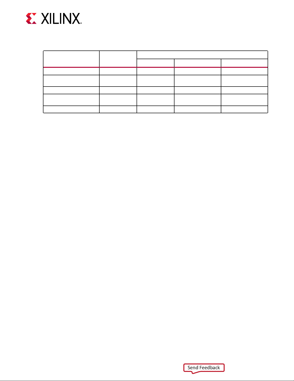
Chapter 2: Shared Features
Send Feedback
Table 19: Recommended Receiver Resets for Common Situations (cont'd)
Situation
After connecting RXN/RXP Entire RX
After recovered clock
becomes stable
After RX elastic buffer error RX PCS
After PRBS error
Eye Scan reset only Eye Scan
Notes:
1. RXPCSRESETMASK[1] can be set to 0 if the FEC is bypassed.
Components
to be Reset
RX PCS
PRBS Error
Counter
RXRESETMODE RXPMARESETMASK RXPCSRESETMASK
2'b00 8’b11111111 4’b1111
2'b11 8’b00000000 4’b1111
2'b11 8’b00000000 4’b1111
2'b11 8’b00000000 4’b1000
2'b11 8’b00000000 4’b0001
Recommended RX Reset Setting
After Power-up and Configuration
The PLL being used and the enre GTM RX require a reset aer conguraon. See GTM
Transceiver RX Reset in Response to Compleon of Conguraon.
After Turning on a Reference Clock to the PLL Being Used
1
If the reference clock(s) changes or GTM transceiver(s) are powered up aer conguraon,
perform a full RX sequenal reset aer the PLL fully completes its reset procedure.
After Changing the Reference Clock to the PLL Being Used
Whenever the reference clock input to the PLL is changed, the PLL must be reset aerwards to
ensure that it locks to the new frequency. Perform a full RX sequenal reset aer the PLL fully
completes its reset procedure.
After Assertion/Deassertion of PLLPD for the PLL Being Used
When the PLL being used goes back to normal operaon aer power down, the PLL must be
reset. Perform a full RX sequenal reset aer the PLL fully completes its reset procedure.
After Assertion/Deassertion of RXPD
Aer the RXPD signal is deasserted, perform a full RX sequenal reset.
UG581 (v1.0) January 4, 2019 www.xilinx.com
Virtex UltraScale+ GTM Transceivers 43
Page 44

Chapter 2: Shared Features
Send Feedback
RX Rate Change
When a rate change is performed, a full RX sequenal reset is required aer the rate aributes
have been updated.
RX Parallel Clock Source Reset
The clocks driving RXUSRCLK must be stable for correct operaon. Perform an RX PCS reset
aer the clock source re-locks.
After Remote Power-Up
If the source of incoming data is powered up aer the GTM transceiver that is receiving its data
has begun operang, a full RX sequenal reset must be performed to ensure a clean lock to the
incoming data.
After Connecting RXN/RXP
When the RX data to the GTM transceiver comes from a connector that can be plugged in and
unplugged, a full RX sequenal reset must be performed when the data source is plugged in to
ensure that it can lock to incoming data.
After Recovered Clock Becomes Stable
Depending on the design of the clocking scheme, it is possible for the RX reset sequence to be
completed before the CDR is locked to the incoming data. In this case, the recovered clock might
not be stable when RXRESETDONE is asserted. When the RX buer is used, a single mode reset
targeng the RX elasc buer must be triggered aer the recovered clock becomes stable.
Refer to the UltraScale+ device device data sheets (see hp://www.xilinx.com/documentaon)
for successful CDR lock-to-data criteria.
After an RX Elastic Buffer Error
Aer an RX elasc buer overow or underow, a sequenal component reset targeng the RX
PCS must be triggered to ensure correct behavior.
UG581 (v1.0) January 4, 2019 www.xilinx.com
Virtex UltraScale+ GTM Transceivers 44
After a PRBS Error
PRBSCNTRESET is asserted to reset the PRBS error counter.
Page 45

Chapter 2: Shared Features
Send Feedback
Power Down
The GTM transceiver oers dierent levels of power control. Each channel in each direcon can
be powered down separately. The PLLPD port directly aects the LCPLL.
Ports and Attributes
The following table denes the power-down ports.
Table 20: Power-Down Ports
Port Dir Clock Domain Description
PLLPD In Async This active-Low signal powers down the LCPLL.
The following table denes the power-down aributes.
Table 21: Power-Down Attributes
Attribute Type Description
CH[0/1]_TX_ANA_CFG0 16-bit Reserved.
Bit Name Address Description
TXPWRDN_B [1:0] Powers down channel TX:
2’b00: Power down.
2’b11: Power up.
RST_CFG 16-bit Reserved.
Bit Name Address Description
RX_PDB_CH0 [2] This active-Low signal powers down channel 0 RX.
RX_PDB_CH1 [3] This active-Low signal powers down channel 1 RX.
PLL Power Down
To acvate the LCPLL power-down mode, the acve-Low PLLPD signal is asserted. When PLLPD
is deasserted, the LCPLL is powered down. As a result, all clocks derived from the PLL are
stopped. Recovery from this power state is indicated by the PLL lock signal PLLLOCK.
UG581 (v1.0) January 4, 2019 www.xilinx.com
Virtex UltraScale+ GTM Transceivers 45
TX and RX Power Down
TX and RX power control signals can be used independently. Only two power states are
supported, as shown in the following table. Powering up/down mulple lanes in a Dual or
mulple Duals aects the power supply regulaon circuit (see Power Up/Down and Reset on
Mulple Lanes).
Page 46

Chapter 2: Shared Features
Send Feedback
Table 22: TX and RX Power Control Signals
Bit Name Value Description
TXPWRDN_B
TXPWRDN_B
[RX_PDB_CH0, RX_PDB_CH1]
[RX_PDB_CH0, RX_PDB_CH1]
2’b11
2’b00
2’b11
2’b00
Normal mode. Transceiver TX is actively sending data.
Power-down mode. Transceiver TX is idle.
Normal mode. Transceiver RX for channel 0 and channel 1 are
actively receiving data.
Power-down mode. Transceiver RX for channel 0 and channel
1 are idle.
Loopback
Loopback modes are specialized conguraons of the transceiver datapath where the trac
stream is folded back to the source. Typically, a specic paern is transmied then compared to
check for errors. The following gure illustrates a loopback test conguraon with three dierent
loopback modes.
Figure 21: Loopback Testing Overview
Link Near-End Test Structures Link Far-End Test Structures
Near-End GTM Transceiver Far-End GTM Transceiver
Test Logic
TX-PMA
2 3
RX-PMA
TX-PCS
`
RX-PCS
X20907-061918
Traffic
Checker
Traffic
Generator
RX-PCS
TX-PCS TX-PMA
1
RX-PMA
RX PMA
Loopback test modes fall into two broad categories:
• Near-end loopback modes loop transmit data back in the transceiver closest to the trac
generator.
• Far-end loopback modes loop received data back in the transceiver at the far end of the data
link.
UG581 (v1.0) January 4, 2019 www.xilinx.com
Virtex UltraScale+ GTM Transceivers 46
Loopback tesng can be used either during development or in deployed equipment for fault
isolaon. The trac paerns used can be either applicaon trac paerns or specialized
pseudo-random bit sequences. Each GTM transceiver has a built-in PRBS generator and checker.
Page 47

Chapter 2: Shared Features
Send Feedback
Each GTM transceiver features several loopback modes to facilitate tesng:
• Near-end PCS Loopback (Path 1 in the above gure). While in Near-end PCS Loopback, the RX
XCLK domain is clocked by the TX parallel clock (TX XCLK).
• Near-end PMA loopback (path 2 in the above gure).
• Far-end PCS Loopback (path 3 in the above gure). The transceiver in far-end PCS loopback
must use the same reference clock used by the transceiver that is the source of the loopbak
data.
Ports and Attributes
The following table denes the loopback ports.
Table 23: Loopback Ports
Port Dir
CH[0/1]_LOOPBACK[2:0] In Async Loopback control for channel 0/1:
Clock
Domain
Description
3’b000: Normal operation.
3’b001: Near-End PCS Loopback.
3’b010: Near-End PMA Loopback.
3’b011: Reserved.
3’b100: Reserved.
3’b101: Reserved.
3’b110: Far-End PCS Loopback.
The following table denes the loopback aributes.
Table 24: Loopback Attributes
Attribute Type Description
CH[0/1]_TX_LPBK_CFG0 16-bit Reserved. Use the recommended value from the Wizard.
CH[0/1]_TX_LPBK_CFG1 16-bit Reserved. Use the recommended value from the Wizard.
UG581 (v1.0) January 4, 2019 www.xilinx.com
Virtex UltraScale+ GTM Transceivers 47
Dynamic Reconfiguration Port
The dynamic reconguraon port (DRP) allows the dynamic change of parameters of the
GTM_DUAL primives. The DRP interface is a processor-friendly synchronous interface with an
address bus (DRPADDR) and separate data buses for reading (DRPDO) and wring (DRPDI)
conguraon data to the primives. An enable signal (DRPEN), a read/write signal (DRPWE), and
a ready/valid signal (DRPRDY) are the control signals that implement read and write operaons,
indicate operaon compleon, or indicate the availability of data.
Page 48

Ports and Attributes
Send Feedback
The following table shows the DRP related ports for the GTM_DUAL.
Table 25: DRP Ports of GTM_DUAL
Chapter 2: Shared Features
Port Dir
DRPADDR[10:0] In DRPCLK DRP address bus.
DRPCLK In N/A DRP interface clock.
DRPEN In DRPCLK DRP enable signal.
DRPDI[15:0]
DRPRDY Out DRPCLK Indicates operation is complete for write operations and data is valid
DRPDO[15:0]
DRPWE In DRPCLK DRP write enable.
In DRPCLK Data bus for writing configuration data from the interconnect logic
Out DRPCLK Data bus for reading configuration data from the GTM transceiver to
Clock
Domain
Description
0: No read or write operation performed.
1: Enables a read or write operation.
For write operations. DRPWE and DRPEN should be driven High for
one DRPCLK cycle only. See Figure 22 for correct operation. For read
operations, DRPEN should be driven High for one DRPCLK cycle only.
See Figure 23 for correct operation.
resources to the transceivers.
for read operations. If writing or reading a R/W register, DRPRDY
asserts six DRPCLK cycles after initiating a DRP transaction. For readonly registers, the number of DRPCLK cycles for DRPRDY assertion
depends on the relationship between the DRPCLK frequency and the
USRCLK frequency. For read-only registers, if a DRPRDY is not seen
within 500 DRPCLK cycles after initiating a DRP transaction, reset the
DRP interface.
the interconnect logic resources.
0: Read operation when DRPEN = 1.
1: Write operation when DRPEN is 1.
For write operations, DRPWE and DRPEN should be driven High for
one DRPCLK cycle only. See Figure 22 for correct operation.
DRPRST
In DRPCLK DRP reset. Reading read-only registers while the XCLK is not toggling
(e.g., during reset or change of reference clocks) causes the DRP to
not return a DRPRDY signal and prevent further DRP transactions. In
such an event, DRPRST must be pulsed to reset the DRP interface
before initiating further DRP transactions.
Usage Model
Write Operation
The following gure shows the DRP write operaon ming. New DRP operaons can be iniated
when DRPRDY is asserted.
UG581 (v1.0) January 4, 2019 www.xilinx.com
Virtex UltraScale+ GTM Transceivers 48
Page 49

DRPCLK
Send Feedback
DRPEN
DRPRDY
DRPWE
Chapter 2: Shared Features
Figure 22: DRP Write Timing
DRPADDR
DRPDI
DRPDO
ADR
DAT
X20218-052318
Read Operation
The following gure shows the DRP read operaon ming. New DRP operaons can be iniated
when DRPY is asserted.
Figure 23: DRP Read Timing
DRPCLK
DRPEN
DRPRDY
UG581 (v1.0) January 4, 2019 www.xilinx.com
Virtex UltraScale+ GTM Transceivers 49
DRPWE
DRPADDR
DRPDI
DRPDO
ADR
DAT
X20219-052318
Page 50

Chapter 2: Shared Features
Send Feedback
Digital Monitor
The receiver uses an adapve algorithm in opmizing a link. The digital monitor provides visibility
into the current state of these adaptaon loops. Digital monitor requires a clock such as
DRPCLK. CH0/1_RXUSRCLK2 can be used for this. The aributes
CH0/1_RX_APT_CFG14A[15:12] and CH0/1_RX_APT_CFG18B[15:12] select the adaptaon
loops monitored on the CH0_DMONITOROUT and CH1_DMONITOROUT ports. The output
ports CH0_DMONITOROUT and CH1_DMONITOROUT contain the current code(s) for a
selected loop. A loop has three steady states: min, max, or dithering.
Ports and Attributes
The following table shows the GTM digital monitor ports.
Table 26: Digital Monitor Ports
Port Dir Clock Domain Description
CH[0/1]_DMONITOROUT[31:0] Out Async/Local Clock Digital monitor output bus for channel
CH[0/1]_DMONITORCLK In Async Channel 0/1 digital monitor clock.
CH[0/1]_DMONITORFIFORESET In Async Reserved. Tie to GND.
CH[0/1]_DMONITOROUTCLK Out Async Channel 0/1 internal clock from
DMONITOROUTPLLCLK Out Async Internal TX calibration clock.
0/1.
adaptation loops.
The following table shows the GTM digital monitor aributes.
Table 27: Digital Monitor Attributes
Attribute Type Description
CH[0/1]_RX_MON_CFG 16-bit Reserved.
Bit Name Bit Field Description
DMON_ENABLE [0] Enables digital monitor for channel 0/1.
DMON_SRC [2:1] Enables RX DMON path for channel 0/1. Must be set to 2’b00 when
reading RX adaptation loops.
UG581 (v1.0) January 4, 2019 www.xilinx.com
Virtex UltraScale+ GTM Transceivers 50
Page 51

Table 27: Digital Monitor Attributes (cont'd)
Send Feedback
Attribute Type Description
CH[0/1]_RX_APT_CFG8B 16-bit Reserved.
Bit Name Bit Field Description
DEMONCON [14:12] Selector for DMON data for channel 0/1.
3’b000: Reserved.
3’b001: Reserved.
3’b010: Reserved.
3’b011: Choose FFE data through FFELOOPSEL.
3’b100: Choose DFE data through DFELOOPSEL.
3’b101: Reserved.
3’b110: Reserved.
3’b111: Reserved.
Chapter 2: Shared Features
CH[0/1]_RX_APT_CFG12B
Bit Name Bit Field Description
TESTSEL [15] Must be set to 1’b0 when reading adaptation loops in channel 0/1.
CH[0/1]_RX_APT_CFG18A 16-bit Reserved.
Bit Name Bit Field Description
DFELOOPSEL [15:12] Selector to monitor DFE and CTLE adaptation loops for channel 0/1.
16-bit Reserved.
Value Adaptation Loop
4’b0100
4’b0110
4’b0111
4’b1000
4’b1001
DFE Tap 1.
AGC frequency gain.
Low frequency gain.
High frequency gain.
Base line wander cancellation.
UG581 (v1.0) January 4, 2019 www.xilinx.com
Virtex UltraScale+ GTM Transceivers 51
Page 52

Chapter 2: Shared Features
Send Feedback
Table 27: Digital Monitor Attributes (cont'd)
Attribute Type Description
CH[0/1]_RX_APT_CFG14B 16-bit Reserved.
Bit Name Bit Field Description
FFELOOPSEL [15:12] Selector to monitor FFE adaptation loops for channel 0/1.
Value Adaptation Loop
4’b0001
4’b0010
4’b0011
4’b0100
4’b0101
4’b0110
4’b0111
4’b1000
4’b1001
4’b1010
4’b1011
4’b1100
4’b1101
4’b1110
FFE tap hm01.
FFE tap hm02.
FFE tap hm03.
FFE tap hm04.
FFE tap hp02.
FFE tap hp03.
FFE tap hp04.
FFE tap hp05.
FFE tap hp06.
FFE tap hp07.
FFE tap hp08.
FFE tap hp09.
FFE tap hp10.
FFE tap hp11.
Use Mode
Reading loop values out of Digital Monitor requires a clock on input port
CH0/1_DMONITORCLK, change adaptaon loop select through DRP, and monitor output
CH0/1_DMONITOROUT. Set aributes DMON_ENABLE, DMON_SRC, DEMONCON, TESTSEL,
and DFELOOPSEL, or FFELOOPSEL via DRP port to enable the digital monitor and select the
appropriate loop for monitoring. The DRP locaons of the aributes are follows.
Channel 0:
• 0x082[0]: DMON_ENABLE
• 0x082[2:1]: DMON_SRC
• 0x033[14:12]: DEMONCON
• 0x03B[15]: TESTSEL
• 0x046[15:12]: DFELOOPSEL
• 0x03f[15:12]: FFELOOPSEL
Channel 1:
• 0x282[0]: DMON_ENABLE
UG581 (v1.0) January 4, 2019 www.xilinx.com
Virtex UltraScale+ GTM Transceivers 52
Page 53

• 0x282[2:1]: DMON_SRC
Send Feedback
• 0x233[14:12]: DEMONCON
• 0x23B[15]: TESTSEL
• 0x246[15:12]: DFELOOPSEL
• 0x23f[15:12]: FFELOOPSEL
Chapter 2: Shared Features
UG581 (v1.0) January 4, 2019 www.xilinx.com
Virtex UltraScale+ GTM Transceivers 53
Page 54

Transmitter
Send Feedback
This chapter shows how to congure and use each of the funconal blocks inside the transmier
(TX). Each transceiver includes an independent transmier, which consist of a PCS and a PMA.
The following gure shows the funconal blocks of the transmier. Parallel data ows from the
device logic into the TX interface through the PCS and PMA, and then out the TX driver as highspeed serial data.
Figure 24: GTM Transceiver TX Block Diagram
Chapter 3: Transmitter
Chapter 3
TX
Driver
TX
Pre/
Pre2/
Post
Emp
PIS
O
TX PMA
Pre-
Coder
TX PCS
To RX Parallel
Data (Near-End
PCS Loopback)
Gray
Encoder
Polarity
The key elements within the GTM transceiver TX are:
1. TX Interface
2. TX FEC
3. TX Buer
4. TX Paern Generator
5. TX Polarity Control
6. TX Gray Encoder
Pattern
Generator
FIFO
FEC
TX
Interface
From RX Parallel
Data (Far-End
PCS Loopback)
X20910-052818
UG581 (v1.0) January 4, 2019 www.xilinx.com
Virtex UltraScale+ GTM Transceivers 54
7. TX Pre-Coder
8. TX Fabric Clock Output Control
9. TX Congurable Driver
Page 55
Chapter 3: Transmitter
Send Feedback
TX Interface
The TX interface is the gateway to the TX datapath of the GTM transceiver. Applicaons
transmit data through the GTM transceiver by wring data to the TXDATA port on the posive
edge of TXUSRCLK2. Port widths can be 64 and 128 bits for NRZ mode, or 80, 128, 160, and
256 bits for PAM4 mode. The rate of the parallel clock (TXUSRCLK2) at the interface is
determined by the TX line rate and the width of the TXDATA port. A second parallel clock
(TXUSRCLK) must be provided for the internal PCS logic in the transmier. This secon shows
how to drive the parallel clocks and explains the constraints on those clocks for correct
operaon.
Interface Width Configuration
The GTM transceiver contains a 64-bit internal datapath in NRZ mode and an 80-bit and 128-bit
internal datapath in PAM4 mode that is congurable by seng the TX_INT_DATA_WIDTH
aribute. When the FEC is enabled, only the 80-bit internal datapath may be used. The interface
width is congurable by seng the TX_DATA_WIDTH aribute. In NRZ mode,
TX_DATA_WIDTH can be congured to 64 or 128 bits. In PAM4 mode, TX_DATA_WIDTH can
be congured to 80, 128, 160, or 256 bits. When the FEC is enabled, only the 80-bit or 160-bit
data width can be selected.
The following table shows how the interface width for the TX datapath is selected.
Table 28: TX Interface Datapath Configuration
Encoding FEC Allowed?
NRZ No 0 64 0 64
NRZ No 2 128 0 64
PAM4 Yes 1 80 1 80
PAM4 Yes 3 160 1 80
PAM4 No 2 128 2 128
PAM4 No 4 256 2 128
TX_DATA_WIDTH
Encoding
TX Data Width
Selection
TX_INT_DATA_WI
DTH Encoding
TX Internal
Datapath
Selection
The following gure shows how the TX data is transmied.
UG581 (v1.0) January 4, 2019 www.xilinx.com
Virtex UltraScale+ GTM Transceivers 55
Page 56

Figure 25: TX Data Transmitted
TXUSRCLK Rate =
Line Rate
Internal Datapath Width
Send Feedback
Chapter 3: Transmitter
UG581 (v1.0) January 4, 2019 www.xilinx.com
Virtex UltraScale+ GTM Transceivers 56
TXUSRCLK and TXUSRCLK2 Generation
The TX interface includes two parallel clocks: TXUSRCLK and TXUSRCLK2. TXUSRCLK is the
internal clock for the PCS logic in the GTM transmier. The required rate for TXUSRCLK
depends on the internal datapath width of the GTM_DUAL primive and the TX line rate of the
GTM transmier. The following equaon shows how to calculate the required rate for
TXUSRCLK for all cases.
Page 57

Chapter 3: Transmitter
Send Feedback
TXUSRCLK2 is the main synchronizaon clock for all signals into the TX side of the GTM
transceiver. Most signals into the TX side of the GTM transceiver are sampled on the posive
edge of TXUSRCLK2. TXUSRCLK2 and TXUSRCLK have a xed-rate relaonship based on the
TX_DATA_WIDTH and TX_INT_DATA_WIDTH sengs. The following table shows the
relaonship between TXUSRCLK2 and TXUSRCLK per TX_DATA_WIDTH and
TX_INT_DATA_WIDTH values.
Table 29: Relationship between TXUSRCLK2 and TXUSRCLK
Encoding TX Data Width TX Internal Datapath TXUSRCLK2 Frequency
NRZ 64 64 F
NRZ 128 64 F
PAM4 80 80 F
PAM4 160 80 F
PAM4 128 128 F
PAM4 256 128 F
TXUSRCLK2
TXUSRCLK2
TXUSRCLK2
TXUSRCLK2
TXUSRCLK2
TXUSRCLK2
= F
= F
= F
= F
= F
= F
TXUSRCLK
TXUSRCLK
TXUSRCLK
TXUSRCLK
TXUSRCLK
TXUSRCLK
/2
/2
/2
These rules about the relaonships between clocks must be observed for TXUSRCLK and
TXUSRCLK2:
• TXUSRCLK and TXUSRCLK2 must be posive-edge aligned, with as lile skew as possible
between them. As a result, low-skew clock resources (BUFG_GTs) must be used to drive
TXUSRCLK and TXUSRCLK2.
• Even though they might run at dierent frequencies, TXUSRCLK, TXUSRCLK2, and the
transmier reference clock must have the same oscillator as their source. Thus TXUSRCLK
and TXUSRCLK2 must be mulplied or divided versions of the transmier reference clock.
Ports and Attributes
The following table denes the TX interface ports.
Table 30: TX Interface Ports
Port Dir Clock Domain Description
TXDATA[255:0] In TXUSRCLK2 The bus for transmitting data. The width of this port
is equal to the TX data width selection.
64: TXDATA[63:0].
80: TXDATA[79:0].
128: TXDATA[127:0].
160: TXDATA[159:0].
256: TXDATA[255:0].
UG581 (v1.0) January 4, 2019 www.xilinx.com
Virtex UltraScale+ GTM Transceivers 57
TXUSRCLK
In Clock This port is used to provide a clock for the internal
TX PCS datapath.
Page 58

Chapter 3: Transmitter
Send Feedback
Table 30: TX Interface Ports (cont'd)
Port Dir Clock Domain Description
TXUSRCLK2 In Clock This port is used to synchronize the interconnect
logic with the TX interface. This clock must be
positive-edge aligned to TXUSRCLK.
The following table denes the TX interface aributes.
Table 31: TX Interface Attributes
Attribute Type Description
CH[0/1]_TX_PCS_CFG0 3-bit Reserved.
Bit Name Address Description
TX_DATA_WIDTH [2:0] Sets the bit width of the TXDATA port. When FEC is enabled,
TX_DATA_WIDTH must be set to 160:
0x0: 64-bit fabric mode.
0x1: 80-bit fabric mode.
0x2: 128 bit fabric mode.
0x3: 160-bit fabric mode.
0x4: 256-bit fabric mode.
TX_INT_DATA_WIDTH
GEN_TXUSRCLK
CH[0/1]_A_CH_CFG0
Bit Name Address Description
TX_FABINT_USRCLK_FLOP [0] Determines if port signals are registered again in the
[4:3] Controls the width of the internal TX PCS datapath. 80-bit
internal datapath must be used with 80- or 160-bit fabric
width; 128-bit internal datapath must be used with 128- or
256-bit fabric width; 64-bit internal datapath must be used
with 64- or 128-bit fabric width:
0x0: 64-bit internal datapath mode.
0x1: 80-bit internal datapath mode.
0x2: 128-bit internal datapath mode.
[14] Automatically generate TXUSRCLK from TXUSRCLK2. This is
only applicable when the fabric datapath width is the same as
the internal datapath width.
0x0: Disable automatic TXUSRCLK generation from
TXUSRCLK2.
0x1: Enable automatic TXUSRCLK generation from
TXUSRCLK2.
1-bit Reserved.
TXUSRCLK domain after being registered in the TXUSRCLK2
domain. This attribute only applies if the TX internal datapath
width is the same as the TX interface width, otherwise this
attribute is ignored. Use the recommended value from the
Wizard:
UG581 (v1.0) January 4, 2019 www.xilinx.com
Virtex UltraScale+ GTM Transceivers 58
0x0: Bypass TXUSRCLK flip-flops.
0x1: Enable TXUSRCLK flip-flops.
Page 59

Chapter 3: Transmitter
Send Feedback
Using TXPROGDIVCLK to Drive the TX Interface
Depending on the TXUSRCLK and TXUSRCLK2 frequencies, there are dierent ways UltraScale
architecture clock resources can be used to drive the parallel clock for the TX interface. Figure 26
through Figure 29 show dierent ways clock resources can be used to drive the parallel clocks
for the TX interface.
Depending on the input reference clock frequency and the required line rate, a BUFG_GT with a
properly congured divide seng is required. The UltraScale+ FPGAs GTM Transceivers Wizard
creates a sample design based on dierent design requirements for most cases.
TXPROGDIVCLK Driving GTM Transceiver TX in 64-Bit, 80-Bit, or 128Bit Mode
In the following gure, TXPROGDIVCLK is used to drive TXUSRCLK and TXUSRCLK2 in 64-bit,
80-bit, or 128-bit mode in a single-lane conguraon. In all cases, the frequency of TXUSRCLK2
is equal to TXUSRCLK.
Figure 26: Single Lane—TXPROGDIVCLK Drives TXUSRCLK and TXUSRCLK2 (64-Bit, 80-
Bit, or 128-Bit Mode)
1
Design in UltraScale
Architecture
X20911-111918
UltraScale
Devices GTM
Transceiver
TXPROGDIVCLK
TXUSRCLK2
TXUSRCLK
2,3
TXDATA (TX data width = 64/80/128 bits)
BUFG_GT
2
Notes relevant to the gure:
UG581 (v1.0) January 4, 2019 www.xilinx.com
Virtex UltraScale+ GTM Transceivers 59
1. For details about placement constraints and restricons on clocking resources (such as
BUFG_GT and BUFG_GT_SYNC), refer to the UltraScale Architecture Clocking Resources User
Guide (UG572).
2. F
TXUSRCLK2
= F
TXUSRCLK
.
3. TXUSRCLK can be ed to 1’b0 if GEN_TXUSRCLK = 1’b1.
Page 60

Chapter 3: Transmitter
Send Feedback
Similarly, the following gure shows the same sengs in a mulple-lane conguraon. In a mullane conguraon, the middle-most GTM transceiver should be selected to be the source of
TXPROGDIVCLK. For example, in a mul-lane conguraon of six GTM transceivers consisng
of three conguous Duals, one of the middle GTM transceivers in the middle Dual should be
selected as the source of TXPROGDIVCLK.
Figure 27: Multiple Lanes—TXPROGDIVCLK Drives TXUSRCLK and TXUSRCLK2 (64-Bit,
80-Bit, or 128-Bit Mode)
UltraScale
Devices GTM
Transceiver
BUFG_GT
TXPROGDIVCLK
TXUSRCLK2
TXUSRCLK
2
2,3
TXDATA (TX data width =
64/80/128 bits)
TXUSRCLK2
2
1
Design in UltraScale
Architecture
UG581 (v1.0) January 4, 2019 www.xilinx.com
Virtex UltraScale+ GTM Transceivers 60
UltraScale
Devices GTM
Transceiver
TXUSRCLK
2,3
TXDATA (TX data width = 64/80/128 bits)
X20912-111918
Notes relevant to the gure:
1. For details about placement constraints and restricons on clocking resources (such as
BUFG_GT and BUFG_GT_SYNC), refer to the UltraScale Architecture Clocking Resources User
Guide (UG572).
2. F
TXUSRCLK2
= F
TXUSRCLK
.
Page 61

Chapter 3: Transmitter
Send Feedback
3. TXUSRCLK can be ed to 1’b0 if GEN_TXUSRCLK = 1’b1.
TXPROGDIVCLK Driving GTM Transceiver TX in 128-Bit, 160-Bit, or 256-Bit Mode
In the following gure, TXPROGDIVCLK is used to drive TXUSRCLK and TXUSRCLK2 in 128-bit,
160-bit, or 256-bit mode in a single-lane conguraon. In all cases, the frequency of
TXUSRCLK2 is equal to half of the TXUSRCLK frequency.
Figure 28: Single Lane—TXPROGDIVCLK Drives TXUSRCLK and TXUSRCLK2 (128-Bit,
160-Bit, or 256-Bit Mode)
1
1
Architecture
X20913-111918
UltraScale
Devices GTM
Transceiver
TXPROGDIVCLK
TXUSRCLK
TXUSRCLK2
TXDATA (TX data width = 128/160/256 bits)
2
2
BUFG_GT
÷2
BUFG_GT
÷1
Design in UltraScale
Notes relevant to the gure:
1. For details about placement constraints and restricons on clocking resources (such as
BUFG_GT and BUFG_GT_SYNC), refer to the UltraScale Architecture Clocking Resources User
Guide (UG572).
UG581 (v1.0) January 4, 2019 www.xilinx.com
Virtex UltraScale+ GTM Transceivers 61
2. F
TXUSRCLK2
= F
TXUSRCLK
/2.
Similarly, the following gure shows the same sengs in a mulple-lane conguraon. In a mul-
lane conguraon, the middle-most GTM transceiver should be selected to be the source of
TXPROGDIVCLK. For example, in a mul-lane conguraon of six GTM transceivers consisng
of three conguous Duals, one of the middle GTM transceivers in the middle Dual should be
selected as the source of TXPROGDIVCLK.
Page 62

Chapter 3: Transmitter
Send Feedback
Figure 29: Multiple Lanes—TXPROGDIVCLK Drives TXUSRCLK and TXUSRCLK2 (128-Bit,
160-Bit, or 256-Bit Mode)
UltraScale
Devices GTM
Transceiver
TXPROGDIVCLK
TXUSRCLK
TXUSRCLK2
TXDATA (TX data width = 128/160/256 bits)
2
2
Design in UltraScale
BUFG_GT
÷2
BUFG_GT
÷1
Architecture
1
1
2
2
X20918-111918
UltraScale
Devices GTM
Transceiver
TXUSRCLK
TXUSRCLK2
TXDATA (TX data width = 128/160/256 bits)
Notes relevant to the gure:
1. For details about placement constraints and restricons on clocking resources (BUFG_GT,
BUFG_GT_SYNC, etc.), refer to the UltraScale Architecture Clocking Resources User Guide
(UG572).
2. F
TXUSRCLK2
= F
TXUSRCLK
/2.
UG581 (v1.0) January 4, 2019 www.xilinx.com
Virtex UltraScale+ GTM Transceivers 62
Page 63

Chapter 3: Transmitter
Send Feedback
TX FEC
The Integrated KP4 Reed-Solomon Forward Error Correcon (RS-FEC) provides a robust mul-bit
error detecon/correcon algorithm that protects up to 2 x 58 Gb/s or 1 x 116 Gb/s electrical
and opcal links. This secon describes the operaon of the Integrated KP4 RS-FEC within the
UltraScale+™ device GTM transceivers.
KP4 FEC is based on the RS(544,514) code, which encodes message blocks of 5140 bits to
produce codewords of 5440 bits. For a detailed descripon of the RS-FEC sublayer in Ethernet,
including the denion of the KP4 FEC code, refer to clause 91 of the IEEE Standard for Ethernet
(IEEE Std 802.3-2015). The same FEC code is used in other standards such as OTN FlexO and
Interlaken.
The Integrated KP4 RS-FEC for each GTM dual is composed of two logical slices for each
channel. These can operate as two independent RS-FEC processing units at up to 58 Gb/s each,
or as one unied unit at up to 116 Gb/s. When operang at up to 116 Gb/s, data is transmied
and received over four virtual FEC lanes as described in IEEE 802.3-2015 clause 91. When
operang as 2 x 58 Gb/s, data can be transmied and received over two virtual FEC lanes per
58 Gb/s channel, or as a raw data stream (one virtual lane) with oponal PN scrambling for
backplane operaons. The general principle of operaon of the FEC is the same whichever mode
is chosen.
When RS-FEC is enabled in the transmit direcon, data to be FEC-encoded and transmied is
provided from the fabric to the input of the GTM transceiver. The pre-FEC data must be pre-
formaed to contain zero padding regions where the parity will be inserted. The Integrated KP4
RS-FEC performs RS encoding to ll in the parity space, and (except in raw mode) also performs
symbol distribuon operaons according to the 802.3bj clause 91 specicaon. The encoded
output data from the Integrated KP4 RS-FEC is then presented to the GTM PCS for transmission.
The Integrated KP4 RS-FEC does not navely perform transcoding, alignment marker removal,
alignment marker mapping, or alignment marker inseron operaons in the transmit direcons.
To support protocols such as 100G Ethernet (IEEE 802.3 clause 91) and 50G Ethernet (IEEE
802.3 clause 134) which require 257b transcoding and alignment marker processing, the GTM
Wizard IP can oponally include so logic blocks for these funcons.
Ports and Attributes
The following table shows the TX FEC-related ports for the GTM dual.
Table 32:
CH[0/1]_TXFECRESET In Async Component reset port for TX FEC.
TX FEC Ports
Ports Dir Clock Domain Description
UG581 (v1.0) January 4, 2019 www.xilinx.com
Virtex UltraScale+ GTM Transceivers 63
Page 64

Chapter 3: Transmitter
Send Feedback
Table 32: TX FEC Ports (cont'd)
Ports Dir Clock Domain Description
CH[0/1]_TXDATA[159:0] In CH[0/1]_TXUSRCLK2 Input TX data, must use 160-bit interface
CH[0/1]_TXDATASTART In CH[0/1]_TXUSRCLK2 Start of codeword.
when FEC is enabled.
The transmit poron of the Integrated KP4 RS-FEC operates internally in the CH0_TXUSRCLK
and CH1_TXUSRCLK domains. Data input on CH0_TXDATA is clocked on the rising edge of
CH0_TXUSRCLK2, and data input on CH1_TXDATA is clocked on the rising edge of
CH1_TXUSRCLK2, just as when the FEC is not enabled.
When congured in 100G mode (combined slice 0 and slice 1 operaon), all data from both
channels must be driven by the CH0_TXUSRCLK2 clock. The CH1_TXUSRCLK and
CH1_TXUSRCLK2 inputs can be ed to ground.
The following table shows the TX FEC-related aributes for the GTM dual.
Table 33: TX FEC Attributes
Attribute Type Description
FEC_CFG0 16-bit Reserved.
Bit Name Address Description
FEC_TX0_MODE [3:0] Operation mode for FEC TX slice 0:
4’b0000: FEC is disabled for this channel.
4’b0001: 50G KP4 FEC, 50GAUI-1 format.
4’b0010: 100G KP4 FEC, 100GAUI-2 format.
4’b0101: 50G raw KP4 FEC without scrambling.
4’b1101: 50G raw KP4 FEC with scrambling.
Others: Invalid.
FEC_TX1_MODE
[7:4] Operation mode for FEC TX slice 1:
4’b0000: FEC is disabled for this channel.
4’b0001: 50G KP4 FEC, 50GAUI-1 format.
4’b0010: 100G KP4 FEC, 100GAUI-2 format.
4’b0101: 50G raw KP4 FEC without scrambling.
4’b1101: 50G raw KP4 FEC with scrambling.
Others: Invalid.
UG581 (v1.0) January 4, 2019 www.xilinx.com
Virtex UltraScale+ GTM Transceivers 64
Page 65

Chapter 3: Transmitter
Send Feedback
Usage Model
When FEC is enabled in 50G mode, bit 0 of each TXDATA bus must be the rst bit to be
transmied in me, and bit 159 must be the last bit to be transmied in me. The
TXDATASTART signal must be driven High whenever the TXDATA for the associated channel
contains the rst 160 bits of a codeword. Input codewords must always be aligned so that bit 0
of a codeword is on bit 0 of the TXDATA bus.
When FEC is enabled in 100G mode, bit 0 of CH0_TXDATA must be the rst bit to be
transmied in me, and bit 159 of CH1_TXDATA must be the last bit to be transmied in me.
The CH0_TXDATASTART signal must be driven High whenever the TXDATA buses contain the
rst 320 bits of a codeword. Input codewords must always be aligned so that bit 0 of a codeword
is on bit 0 of CH0_TXDATA. CH1_TXDATASTART is ignored in 100G mode.
In all modes, codewords are 5440 bits in length. The nal 300 bits of data is reserved for the
inseron of FEC parity. At the input to the FEC, bits 5140 to 5439 of the input data must be set
to 0.
50G Ethernet
Up to two channels of 50G Ethernet with KP4 FEC can be implemented as per IEEE Dra
Standard for Ethernet Amendment: Media Access Control Parameters for 50 Gb/s and Physical Layers
and Management Parameters for 50 Gb/s, 100 Gb/s, and 200 Gb/s Operaon (IEEE Std 802.3cd
Clause 134). Transcoding should be enabled in the GTM Wizard IP for this mode. The nominal
pre-FEC PCS data rate is 51.5625 Gb/s, and the nominal post-FEC line rate is 53.125 Gb/s.
100G Ethernet
One channel of 100G Ethernet with KP4 FEC can be implemented as per IEEE Std 802.3-2015
Clause 91. Transcoding should be enabled in the GTM Wizard IP for this mode. The nominal
aggregate pre-FEC PCS data rate is 103.125 Gb/s and the nominal aggregate post-FEC line rate
is 106.25 Gb/s.
100G OTN FlexO
One channel of 100G OTN FlexO with a KP4 FEC can be implemented as per ITU-T G.709.1,
Flexible OTN Short-Reach Interface. Transcoding should be disabled in the GTM Wizard IP for this
mode. The nominal aggregate post-FEC line rate is 111.81 Gb/s.
UG581 (v1.0) January 4, 2019 www.xilinx.com
Virtex UltraScale+ GTM Transceivers 65
100G Interlaken
One channel of 100G Interlaken with KP4 FEC can be implemented as per the Interlaken ReedSolomon Forward Error Correcon Extension Protocol Denion. Transcoding should be disabled in
the GTM Wizard IP for this mode. Line rates up to 58 Gb/s are possible.
Page 66

Chapter 3: Transmitter
Send Feedback
Proprietary Backplane Protocols with FEC up to 58 Gb/s
FEC can be enabled in 50G raw mode (with or without scrambling).
TX Buffer
The GTM transceiver TX datapath has two internal parallel clock domains used in the PCS: the
interface with PMA parallel clock domian (XCLK), and the PCS internal clock domain
(TXUSRCLK). To transmit data, the TX buer provides data width conversion between these
clock domains when necessary, depending on the operang data width and encoding mode. The
following gure shows the TX datapath clock domains.
Figure 30: TX Clock Domains
Device Parallel
TX Serial Clock PMA Parallel Clock (XCLK) PCS Parallel Clock (TXUSRCLK)
Clock
(TXUSRCLK2)
Pattern
Generator
TX
FIFO
FEC
From RX Parallel Data
(Far-End PCS Loopback)
TX
Interface
X20914-053018
Driver
TX
TX
Pre/
Pre
2/
Post
Emp
TX PMA
PISO
Pre-
Coder
TX PCS
To RX Parallel Data
(Near-End PCS Loopback)
Encoder
Gray
Polarity
The GTM transmier includes a TX FIFO to support data width conversion when data crosses
from TXUSRCLK to XCLK domain, and the table below shows the possible scenarios. The buer
does not tolerate ppm dierences, and only provides phase compensaon between the two
clocks. The TX buer inside the GTM transceiver must always be used. Buer bypass is not
allowed.
Table 34: TX FIFO Data Width Conversion Scenarios
PCS Parallel Clock (TXUSRCLK)
Domain Data Width
64-bit 64-bit No
80-bit 128-bit Yes
128-bit 128-bit No
PMA Parallel Clock (XCLK) Domain
Data Width
FEC Support
UG581 (v1.0) January 4, 2019 www.xilinx.com
Virtex UltraScale+ GTM Transceivers 66
Page 67

Ports and Attributes
Send Feedback
The following table denes the TX buer ports.
Table 35: TX Buffer Ports
Port Dir Clock Domain Description
CH[0/1]_TXBUFSTATUS[1:0] Out TXUSRCLK TX buffer status:
Bit[1]: FIFO overflow status. A value of
1 indicates FIFO overflow.
Bit[0]: FIFO underflow status. A value
of 1 indicates FIFO underflow.
Chapter 3: Transmitter
The following table
denes the TX buer aributes.
Table 36: TX Buffer Attributes
Attribute Type Description
CH[0/1]_TX_PCS_CFG0 16-bit Reserved. Use the recommended value from the Wizard.
CH[0/1]_TXFIFO_UNDERFLOW 1-bit A value of 1 indicates FIFO underflow.
For channel 0, bit[8] of DRP address 0x489
For channel 1, bit[8] of DRP address 0x689
Note: This is a read-only aribute.
CH[0/1]_TXFIFO_OVERFLOW
1-bit A value of 1 indicates FIFO overflow.
For channel 0, bit[9] of DRP address 0x489
For channel 1, bit[9] of DRP address 0x689
Note: This is a read-only aribute.
TX Pattern Generator
UG581 (v1.0) January 4, 2019 www.xilinx.com
Virtex UltraScale+ GTM Transceivers 67
Pseudo-random it sequences (PRBS) are commonly used to test the signal integrity of high-speed
links. These sequences appear random but have specic properes that can be used to measure
the quality of a link. The GTM transceiver paern generator block can generate several industrystandard PRBS paerns listed in the following table.
Table 37:
Name Polynomial
PRBS-7 1 + x6 + x
Supported PRBS Patterns
7
Length of
Sequence
27 – 1 bits Used to test channels with 8B/10B.
Description
Page 68

Table 37: Supported PRBS Patterns (cont'd)
Send Feedback
Chapter 3: Transmitter
Name Polynomial
PRBS-9 1 + x5 + x
PRBS-13 1 + x + x2 + x12 + x
PRBS-15 1 + x14 + x
PRBS-23 1 + x18 + x
PRBS-31 1 + x28 + x
9
15
23
31
13
Length of
Sequence
29 – 1 bits ITU-T Recommendation O.150, Section 5.1. PRBS-9 is one
of the recommended test patterns for SFP+.
29 – 1 bits IEEE Std P802.3bs D3.5 test requires QPRBS-13 test
pattern.
215 – 1 bits ITU-T Recommendation O.150, Section 5.3. PRBS-15 is
often used for jitter measurement because it is the
longest pattern the Agilent DCA-J sampling scope can
handle.
223 – 1 bits ITU-T Recommendation O.150, Section 5.6. PRBS-23 is
often used for non-8B/10B encoding schemes. It is one
of the recommended test patterns in the SONET
specification.
231 – 1 bits ITU-T Recommendation O.150, Section 5.8. PRBS-31 is
often used for non-8B/10B encoding schemes. It is a
recommended PRBS test pattern for 10 Gigabit Ethernet.
See IEEE Std 802.3ae-2002.
Description
IMPORTANT! For PAM4 modulaon, QPRBS paerns are supported by sending a convenonal PRBS
paern with PAM4 and Gray Coding based on the OIF2014.230 CEI-56G-VSR-PAM4 specicaon.
In addion to PRBS paerns, the GTM transceiver supports a 64 UI square wave test paern as
shown in the following gure, an alternang 1’b0 and 1’b1 (NRZ clock) test paern. Clocking
paerns are usually used to check PLL random jier oen done with a spectrum analyzer.
Note: For PAM4 modulaon, an alternang 1’b0 and 1’b1 test paern will not be a square wave due to
the amplitude modulaon mapping.
Figure 31: 64 UI Square Wave
64 UI
X22031-112618
The error inseron funcon is also supported to verify link connecon for jier tolerance tests.
When an inverted PRBS paern is necessary, the CH[0/1]_TXPOLARITY signal is used to control
polarity.
UG581 (v1.0) January 4, 2019 www.xilinx.com
Virtex UltraScale+ GTM Transceivers 68
Page 69

PRBS-7
Send Feedback
PRBS-9
PRBS-13
PRBS-15
PRBS-23
PRBS-31
Alternating 1'b0 and 1'b1
Square Wave with 64 UI Period
Figure 32: TX Pattern Generator Block
Error
Insertions
Chapter 3: Transmitter
Polarity
Inversion
CH0/1_TXDATA
FIFO
Ports and Attributes
The following table denes the paern generator ports.
Table 38: Pattern Generator Ports
Port Name Dir Clock Domain Description
CH[0/1]_TXPRBSPTN[3:0] In CH[0/1]_TXUSRCLK2 Transmitter pattern generator control.
4’b0000: Standard operation mode (test
pattern generation is off)
4’b0001: PRBS-7
4’b0010: PRBS-9
4’b0011: PRBS-15
4’b0100: PRBS-23
4’b0101: PRBS-31
4’b0110: PRBS-13
4’b1000: Reserved
4’b1001: Alternating 1b’0 and 1’b1
4’b1010: Square wave with 64 UI period
X22032-112618
UG581 (v1.0) January 4, 2019 www.xilinx.com
Virtex UltraScale+ GTM Transceivers 69
CH[0/1]_TXPRBSINERR In CH[0/1]_TXUSRCLK2 When this port is driven High, a single error is
CH[0/1]_TXQPRBSEN
In CH[0/1]_TXUSRCLK2 Reserved. This port must always be set to 1’b0.
forced in the PRBS transmitter for every
CH[0/1]_TXUSRCLK2 clock cycle that the port is
asserted.
When CH[0/1]_TXPRBSPTN is set to 4’b0000, this
port does not affect CH[0/1]_TXDATA.
The following table denes the paern generator aribute.
Page 70

Chapter 3: Transmitter
Send Feedback
Table 39: Pattern Generator Attribute
Attribute Type Description
CH[0/1]_TX_PCS_CFG1 16-bit Reserved.
Bit Name Address Description
RXPRBSERR_LOOPBACK [7] Setting this attribute to 1’b1 causes the CH[0/1]_RXPRBSERR bit to
be internally looped back to CH[0/1]_TXPRBSINERR of the same
GTM transceiver. This allows synchronous and asynchronous jitter
tolerance testing without worrying about data clock domain
crossing. Setting this attribute to 1’b0 causes
CH[0/1]_TXPRBSINERR to be forced onto the TX PRBS.
Using TX Pattern Generator
The GTM TX paern generator works for all supported data widths. However, 80-bit or 160-bit
TX fabric data width in PAM4 mode requires addional steps. Other data widths do not require
any addional steps.
Enable TX Pattern Generator for 80-bit or 160-bit Data Width
1. Using the DRP interface, write the following values to CH[0/1]_TX_PCS_CFG0[4:0] (address
0x083 for CH0, 0x283 for CH1):
a. CH[0/1]_TX_PCS_CFG0[4:0] = 0x12 for 80-bit data width mode.
b. CH[0/1]_TX_PCS_CFG0[4:0] = 0x14 for 160-bit data width mode.
2. Enable the PRBS generator by seng CH[0/1]_TXPRBSPTN to the required value for the
desired paern.
3. TX PRBS paern generator is enabled.
Note: Toggling CH[0/1]_TXPRBSINSERR for one CH[0/1]_TXUSRCLK2 cycle might inject more than one
error into the paern generator in 80/160 bit mode.
Disable TX Pattern Generator for 80-bit or 160-bit Data Width
1. Disable the PRBS generator by seng CH[0/1]_TXPRBSPTN[3:0] to 4’b0000.
2. Using the DRP interface, write the following values to CH[0/1]_TX_PCS_CFG0[4:0] (address
0x083 for CH0, 0x283 for CH1):
a. CH[0/1]_TX_PCS_CFG0[4:0] = 0x09 for 80-bit data width mode.
UG581 (v1.0) January 4, 2019 www.xilinx.com
Virtex UltraScale+ GTM Transceivers 70
b. CH[0/1]_TX_PCS_CFG0[4:0] = 0x0B for 160-bit data width mode.
3. Set CH[0/1]_TXPMARESETMASK = 0x0.
4. Toggle CH[0/1]_GTTXRESET High and Low.
5. Wait for CH[0/1]_TXRESETDONE to toggle High.
6. Set CH[0/1]_TXPMARESETMASK = 0x3.
Page 71

Chapter 3: Transmitter
Send Feedback
TX PRBS paern generator is disabled and the TX is driven based on the CH[0/1]_TXDATA
input.
TX Polarity Control
If TXP and TXN dierenal traces are accidentally swapped on the PCB, the dierenal data
transmied by the GTM transceiver TX is reversed. One soluon is to invert the parallel data
before serializaon and transmission to oset the reversed polarity on the dierenal pair. The
TX polarity control can be accessed through the CH0_TXPOLARITY and CH1_TXPOLARITY
input from the interconnect logic interface. The TX polarity control is driven High to invert the
polarity of outgoing data.
Ports and Attributes
The following table denes the ports required for TX polarity control.
Table 40: TX Polarity Control Ports
Port Dir Clock Domain Description
CH0_TXPOLARITY
CH1_TXPOLARITY
Notes:
1. CH[0/1]_TXPOLARITY can be tied High if the polarity of TXP and TXN needs to be reversed.
1
1
In CH0_TXUSRCLK2 The CH0_TXPOLARITY port is used to invert the
polarity of the outgoing data for channel 0:
0: Not inverted. TXP is positive, and TXN is
negative.
1: Inverted. TXP is negative, and TXN is
positive.
In CH1_TXUSRCLK2 The CH1_TXPOLARITY port is used to invert the
polarity of the outgoing data for channel 1:
0: Not inverted. TXP is positive, and TXN is
negative.
1: Inverted. TXP is negative, and TXN is
positive.
TX Gray Encoder
UG581 (v1.0) January 4, 2019 www.xilinx.com
Virtex UltraScale+ GTM Transceivers 71
GTM transmiers in UltraScale+ devices support two types of binary encoding opons: linear
coding and Gray coding. By using Gray coding, only one bit error per symbol is made for incorrect
decisions, thus reducing the bit-error rate by more than 33%. The following gure illustrates the
dierences between linear coding and Gray coding.
Page 72

Chapter 3: Transmitter
Send Feedback
Figure 33: Transmitted PAM4 Signal Bit Encoding
Ports and Attributes
The following table denes the aributes required for TX Gray encoder control.
Table 41: Gray Encoder Attributes
Attribute Type Description
CH[0/1]_TX_PCS_CFG0 16-bit Reserved.
Bit Name Address Description
TX_GRAY_ENDIAN [13] In PAM4 mode, this attribute controls transmitted
TX_GRAY_BYP_EN
[12] In PAM4 mode, this attribute enables Gray encoding. In NRZ
endianness. In NRZ mode, the default Wizard value must be
used.
1’b0: Non-inverting.
1’b1: Inverting.
mode, the default Wizard value must be used.
1’b0: Enables Gray encoding.
1’b1: Disables Gray encoding.
IMPORTANT! In PAM4 mode, if Gray encoder is enabled for the transmier, the receiver Gray decoder
should also be enabled for proper data recovery.
TX Pre-Coder
UG581 (v1.0) January 4, 2019 www.xilinx.com
Virtex UltraScale+ GTM Transceivers 72
GTM transmiers in UltraScale+ devices support pre-coding. Pre-coding can be used to reduce
receiver decision feedback equalizaon (DFE) error propagaon by reducing 1-tap burst error
runs into two errors for every error event.
Page 73

Chapter 3: Transmitter
Send Feedback
Ports and Attributes
The following table denes the aributes required for TX pre-coder control.
Table 42: Pre-Coder Attributes
Attribute Type Description
CH[0/1]_TX_PCS_CFG0 16-bit Reserved.
Bit Name Address Description
TX_PRECODE_ENDIAN [11] In PAM4 mode, this attribute controls pre-coder
transmitted endianness. In NRZ mode, the default
Wizard value must be used.
1’b0: Non-inverting.
1’b1: Inverting.
TX_PRECODE_BYP_EN
[10] In PAM4 mode, this attribute enables pre-coding. In
NRZ mode, the default Wizard value must be used.
1’b0: Enables pre-code.
1’b1: Disables pre-code.
IMPORTANT! In PAM4 mode, if pre-coder is enabled for the transmier, the receiver pre-coder should
also be enabled for proper data recovery.
TX Fabric Clock Output Control
The TX Clock Divider Control block has two main components: serial clock divider control, and
parallel clock divider and selector control. The clock divider and selector details are illustrated in
the following gure.
UG581 (v1.0) January 4, 2019 www.xilinx.com
Virtex UltraScale+ GTM Transceivers 73
Page 74

Figure 34: TX Serial and Parallel Clock Divider
Send Feedback
GTM_DUAL (GTM Transceiver Primitive)
Chapter 3: Transmitter
TXP/N
MGTREFCLKP
MGTREFCLKN
PISO
TX CLKGEN
LCPLL
REFCLK SEL
REFCLK
Distribution
IBUFDS_GTM
/32
TX PROG
DIV
O
ODIV2
TX DATA
Output to
GTM_DUAL
TX PCSTX PMA
Polarity
Control
Pre-
Coder
Gray
Encoder
CH[0/1]_TXPROGDIVCLK
Output Clock to BUFG_GT
TX FIFO
TX DATA from
Upstream PCS Blocks
CH[0/1]_TXUSRCLK
REFCLK_HROW_CK_SEL
Notes relevant to the gure:
1. CH[0/1]_TXPROGDIVCLK is used as the source of the interconnect logic clock via BUFG_GT.
2. There is only one LCPLL in the GTM_DUAL primive, which is shared between the TX/RX.
TX Programmable Divider
The TX programmable divider shown in Figure 34 uses the LCPLL output clock to generate a
parallel output clock. By using the transceiver LCPLL, TX programmable divider, and BUFG_GT,
CH[0/1]_TXPROGDIVCLK should be used as a clock source for the interconnect logic.
The following tables show the programmable divider ports and aributes, respecvely.
X20915-110218
UG581 (v1.0) January 4, 2019 www.xilinx.com
Virtex UltraScale+ GTM Transceivers 74
Page 75

Chapter 3: Transmitter
Send Feedback
Table 43: TX Programmable Divider Ports
Port Dir Clock Domain Description
CH[0/1]_TXPROGDIVRESET In Async This active-High port resets the dividers as well
CH[0/1]_TXPRGDIVRESETDONE Out Async When the input clock is stable and reset is
CH[0/1]_TXPROGDIVCLK Out Clock TXPROGDIVCLK is the parallel clock output from
as the TXPRGDIVRESETDONE indicator. A reset
must be performed whenever the input clock
source is interrupted.
performed, this active-High signal indicates the
reset is completed and the output clock is
stable.
the TX programmable divider. This clock is the
recommended output to the interconnect logic
through BUFG_GT.
Table 44: TX Programmable Divider Attribute
Attribute Type Description
CH[0/1]_TX_DRV_CFG4 16-bit Reserved.
Bit Name Address Description
TX_PROGDIV_SEL_FULLRATE [15] This attribute is used during the TX programmable divider
ratio selection. Set to 1’b1 to obtain the full rate of the
divided clock. Set to 1’b0 to obtain the half rate of the
divided clock.
UG581 (v1.0) January 4, 2019 www.xilinx.com
Virtex UltraScale+ GTM Transceivers 75
Page 76

Chapter 3: Transmitter
Send Feedback
Table 44: TX Programmable Divider Attribute (cont'd)
Attribute Type Description
TX_PROGDIV_FBKDIV [11:6] This attribute is the main TX programmable divider selector.
When the following settings are set:
TX_PROGDIV_SEL_DIV66 = 1’b1
TX_PROGDIV_PDBV_DIV5 = 1’b0
TX_PROGDIV_SEL_FULLRATE = 1’b1 (or 1’b0)
Valid TX programmable divider ratios are:
6'b011000: 4 (8)
6'b111000: 5 (10)
6'b000000: 8 (16)
6'b100000: 10 (20)
6'b000001: 12 (24)
6'b100001: 15 (30)
6'b000010: 16 (32)
6'b100010: 20 (40)
6'b000101: 24 (48)
6'b100011: 25 (50)
6'b100101: 30 (60)
6'b000110: 32 (64)
6'b100110: 40 (80)
6'b001101: 48 (96)
6'b100111: 50 (100)
6'b101101: 60 (120)
6'b001110: 64 (128)
6'b001111: 80 (160)
6'b101111: 100 (200)
UG581 (v1.0) January 4, 2019 www.xilinx.com
Virtex UltraScale+ GTM Transceivers 76
When the following settings are set:
TX_PROGDIV_SEL_DIV66 = 1’b0
TX_PROGDIV_PDBV_DIV5 = 1’b1
TX_PROGDIV_SEL_FULLRATE = 1’b1 (or 1’b0)
Valid TX programmable divider ratios are:
6'b011000: 16.5 (33)
6'b000000: 33 (66)
6'b000010: 66 (132)
TX_PROGDIV_SEL_DIV66 [3] This attribute is used during the TX programmable divider
ratio selection.
• The attribute must be set to 1’b1 when the desired
divider value is either 16.5, 33, 66, or 132.
• For all other divider values, this should be set to 1’b0.
Page 77

Chapter 3: Transmitter
Send Feedback
Table 44: TX Programmable Divider Attribute (cont'd)
Attribute Type Description
TX_PROGDIV_PDBV_DIV5 [2] This attribute is used during the TX programmable divider
ratio selection.
• The attribute must be set to 1’b0 when the desired
divider value is either 16.5, 33, 66, or 132.
• For all other divider values, this should be set to 1’b1.
Ports and Attributes
The following table denes the ports required for TX fabric clock output control.
Table 45: TX Fabric Clock Output Control Ports
Port Dir
CH[0/1]_TXOUTCLKSEL[2:0] In Async This port must be set to 3'b000.
CH[0/1]_TXOUTCLK Out Clock Reserved.
CH[0/1]_TXPROGDIVCLK Out Clock TXPROGDIVCLK is the parallel output clock from the
Clock
Domain
Description
TX programmable divider. This clock is the
recommended output to the interconnect logic
through BUFG_GT.
TX Configurable Driver
The GTM transceiver TX driver is a high-speed voltage-mode dierenal output buer. To
maximize signal integrity, it includes these features:
• Dierenal voltage control
• Two pre-cursor, and one post-cursor transmit pre-emphasis
• Two modulaon schemes: NRZ and PAM4
• Calibrated terminaon resistors
UG581 (v1.0) January 4, 2019 www.xilinx.com
Virtex UltraScale+ GTM Transceivers 77
Page 78

Figure 35: TX Configurable Driver Block Diagram
Send Feedback
CH0/1_TXEMPPRE2[3:0]
Pre-Emphasis 2
Pad Driver
CH0/1_TXEMPPRE[4:0]
Pre-Emphasis
Pad Driver
Chapter 3: Transmitter
PISO
4-Tap
FIR
CH0/1_TXDRVAMP[4:0]
Main
Pad Driver
CH0/1_TXEMPPOST[4:0]
Post-Emphasis
Pad Driver
50Ω
CH0/1_GTMTXP
50Ω
CH0/1_GTMTXN
Ports and Attributes
The following table denes the TX congurable driver ports.
Table 46: TX Configurable Driver Ports
Port Dir
CH[0/1]_TXDRVAMP[4:0] Input Async Driver swing control. The default is user specified. All listed
Clock
Domain
values are in mV
[4:0] mV
5’b00000
5’b00001
5’b00010
5’b00011
5’b00100
5’b00101
5’b00110
PPD
Description
.
PPD
250
275
300
325
350
375
400
X20916-060618
UG581 (v1.0) January 4, 2019 www.xilinx.com
Virtex UltraScale+ GTM Transceivers 78
Page 79

Table 46: TX Configurable Driver Ports (cont'd)
Send Feedback
Chapter 3: Transmitter
Port Dir
CH[0/1]_TXINHIBIT
CH[0/1]_TXEMPMAIN[5:0] Input Allows the main cursor coefficients to be directly set if
Input TXUSRCLK2 When High, this signal blocks transmission of CH[0/1]_TXDATA
Clock
Domain
Description
5’b00111
5’b01000
5’b01001
5’b01010
5’b01011
5’b01100
5’b01101
5’b01110
5’b01111
5’b10000
5’b10001
5’b10010
5’b10011
5’b10100
5’b10101
5’b10110
5’b10111
5’b11000
5’b11001
5’b11010
5’b11011
5’b11100
5’b11101
5’b11110
5’b11111
Notes:
1. The peak-to-peak differential voltage is defined when
CH[0/1]_TXEMPPOST = 5’b00000, CH[0/1]_TXEMPPRE =
5’b00000, and CH[0/1]_TXEMPPRE2 = 4’b0000.
2. For UltraScale+ FPGAs, the output swing described above
is obtained using settings from the Wizard design, and the
recommended values from the Wizard should not be
changed.
and forces CH[0/1]_GTMTXP to 0 and CH[0/1]_GTMTXN to 1.
CH[0/1]_TX_DRV_CFG0[0] attribute is set to 1’b1.
CH[0/1]_TXDRVAMP should be used together with
CH[0/1]_TXEMPMAIN to achieve the desired TX output swing.
425
450
475
500
525
550
575
600
625
650
675
700
725
750
775
800
825
850
875
900
925
950
975
1000
1025
UG581 (v1.0) January 4, 2019 www.xilinx.com
Virtex UltraScale+ GTM Transceivers 79
Page 80
Table 46: TX Configurable Driver Ports (cont'd)
Send Feedback
Chapter 3: Transmitter
Port Dir
CH[0/1]_TXEMPPRE[4:0] Input Async Transmitter pre-cursor TX pre-emphasis control. The default is
Clock
Domain
Description
user specified. All listed values (dB) are typical
[4:0] dB (PAM4) dB (NRZ) Coefficient
5’b00000
5’b00001
5’b00010
5’b00011
5’b00100
5’b00101
5’b00110
5’b00111
5’b01000
5’b01001
5’b01010
5’b01011
5’b01100
5’b01101
5’b01110
5’b01111
5’b10000
5’b10001
5’b10010
5’b10011
5’b10100
5’b10101
5’b10110
5’b10111
5’b11000
5’b11001
5’b11010
Notes:
1. The peak-to-peak differential voltage is defined when
CH[0/1]_TXEMPPOST = 5’b00000, and
CH[0/1]_TXEMPPRE2 = 4’b0000. Emphasis =
20log10(V
0.0 0.0 0
–0.3 –0.2 1
–0.7 –0.5 2
–1.1 –0.7 3
–1.5 –0.9 4
–1.9 –1.2 5
–2.3 –1.5 6
–2.7 –1.7 7
–3.2 –2.0 8
–3.7 –2.3 9
–4.2 –2.6 10
–4.8 –2.9 11
–5.4 –3.2 12
–6.0 –3.5 13
–6.7 –3.9 14
–7.5 –4.2 15
–8.3 –4.6 16
–9.2 –5.0 17
N/A –5.4 18
N/A –5.8 19
N/A –6.2 20
N/A –6.7 21
N/A –7.2 22
N/A –7.7 23
N/A –8.3 24
N/A –8.9 25
N/A –9.2 26
high/Vlow
) = |20log10(V
low/Vhigh
)|.
Units
UG581 (v1.0) January 4, 2019 www.xilinx.com
Virtex UltraScale+ GTM Transceivers 80
Page 81

Table 46: TX Configurable Driver Ports (cont'd)
Send Feedback
Chapter 3: Transmitter
Port Dir
CH[0/1]_TXEMPPRE2[3:0] Input Async Transmitter pre-cursor 2 TX pre-emphasis control for channel 0.
Clock
Domain
Description
The default is user specified. All listed values (dB) are typical
[4:0] dB (PAM4) dB (NRZ) Coefficient
4’b0000
4’b0001
4’b0010
4’b0011
4’b0100
4’b0101
4’b0110
4’b0111
4’b1000
4’b1001
4’b1010
4’b1011
Notes:
1. The peak-to-peak differential voltage is defined when
CH[0/1]_TXEMPPRE = 5’b00000, and CH[0/1]_TXEMPPOST
= 4’b0000. Emphasis = 20log10(V
20log10(V
0.0 0.0 0
–0.3 –0.2 1
–0.7 –0.5 2
–1.1 –0.7 3
–1.5 –0.9 4
–1.9 –1.2 5
–2.3 –1.5 6
–2.7 –1.7 7
N/A –2.0 8
N/A –2.3 9
N/A –2.6 10
N/A –2.9 11
high/Vlow
low/Vhigh
)|.
Units
) = |
UG581 (v1.0) January 4, 2019 www.xilinx.com
Virtex UltraScale+ GTM Transceivers 81
Page 82

Table 46: TX Configurable Driver Ports (cont'd)
Send Feedback
Chapter 3: Transmitter
Port Dir
CH[0/1]_TXEMPPOST[4:0] Input Async Transmitter post-cursor TX pre-emphasis control for channel 0.
CH[0/1]_GTMTXP
CH[0/1]_GTMTXN
CH[0/1]_TXCTLFIRDAT[5:0] Input Async Reserved. Use the recommended value from the Wizard
CH[0/1]_TXMUXDCDEXHOLD Input Async Reserved. Use the recommended value from the Wizard.
Output
(pad)
Clock
Domain
The default is user specified. All listed values (dB) are typical.
[4:0] dB (PAM4) dB (NRZ) Coefficient
5’b00000
5’b00001
5’b00010
5’b00011
5’b00100
5’b00101
5’b00110
5’b00111
5’b01000
5’b01001
5’b01010
5’b01011
5’b01100
5’b01101
5’b01110
5’b01111
5’b10000
5’b10001
5’b10010
5’b10011
5’b10100
5’b10101
5’b10110
5’b10111
5’b11000
5’b11001
5’b11010
Notes:
1. The peak-to-peak differential voltage is defined when
TXEMPPRE = 5’b00000, and TXEMPPRE2 = 4’b0000.
Emphasis = 20log10(V
TX Serial Clock Differential complements of one another forming a differential
transmit output pair. These ports represent the pads. The
locations of these ports must be constrained (see
Implementation) and brought to the top of the design.
Description
Units
0.0 0.0 0
–0.3 –0.2 1
–0.7 –0.5 2
–1.1 –0.7 3
–1.5 –0.9 4
–1.9 –1.2 5
–2.3 –1.5 6
–2.7 –1.7 7
–3.2 –2.0 8
–3.7 –2.3 9
–4.2 –2.6 10
–4.8 –2.9 11
–5.4 –3.2 12
–6.0 –3.5 13
–6.7 –3.9 14
–7.5 –4.2 15
–8.3 –4.6 16
–9.2 –5.0 17
N/A –5.4 18
N/A –5.8 19
N/A –6.2 20
N/A –6.7 21
N/A –7.2 22
N/A –7.7 23
N/A –8.3 24
N/A –8.9 25
N/A –9.2 26
high/Vlow
) = |20log10(V
low/Vhigh
)|.
UG581 (v1.0) January 4, 2019 www.xilinx.com
Virtex UltraScale+ GTM Transceivers 82
Page 83

Table 46: TX Configurable Driver Ports (cont'd)
Send Feedback
Chapter 3: Transmitter
Port Dir
CH[0/1]_TXMUXDCDORWREN Input Async Reserved. Use the recommended value from the Wizard.
Clock
Domain
Description
The following table denes the TX congurable driver aributes.
Table 47: TX Configurable Driver Attributes
Attribute Type Description
CH[0/1]_TX_ANA_CFG1 16-bit Reserved.
Bit Name Address Description
TXMODSEL [7] Driver output modulation control:
1’b0: PAM4 modulation.
1’b1: NRZ modulation.
CH[0/1]_TX_DRV_CFG0 16-bit Reserved.
Bit Name Address Description
TXEMPMAIN_INDEP [0] Allows independent control of the main cursor:
1’b0: The CH[0/1]_TXEMPMAIN coefficient is
automatically determined.
1’b1: CH[0/1]_TXEMPMAIN coefficient can be
independently set by the CH[0/1]_TXEMPMAIN
pins within the range specified in the pin
description.
UG581 (v1.0) January 4, 2019 www.xilinx.com
Virtex UltraScale+ GTM Transceivers 83
Use Modes
The GTM TX has the ability to transmit serial data using two dierent modulaon schemes: NRZ
and PAM4. NRZ signals contains one bit of informaon per symbol, while PAM4 signals contain
two bits of informaon per symbol. Using PAM4 modulaon doubles the transmied data
bandwidth while maintaining the same unit interval (UI). To program the GTM TX to a desired
signal modulaon mode, the user must congure the aribute TXMODSEL for CH0 or CH1.
Page 84

Receiver
Send Feedback
This secon shows how to congure and use each of the funconal blocks inside the receiver
(RX). Each GTM transceiver includes an independent receiver made up of a PCS and PMA. The
following gure shows the blocks of the GTM transceiver RX. High-speed serial data ows from
traces on the board into the PMA of the GTM transceiver RX, into the PCS, and nally into the
interconnect logic.
Chapter 4: Receiver
Chapter 4
Figure 36: GTM Transciever RX Block Diagram
To RX Parallel Data
(Near-End PCS Loopback)
Gray
Encoder
Polarity
RX EQ SIPOADC
DFE/
FFE
RX PMA
RX PCS
Pre-
Coder
The key elements within the GTM transceiver RX are:
1. RX Analog Front End
2. RX Equalizer
3. RX CDR
4. RX Fabric Clock Output Control
PRBS
Checker
FIFO
From RX Parallel Data
(Far-End PCS Loopback)
FEC
RX
Interface
X20221-053018
UG581 (v1.0) January 4, 2019 www.xilinx.com
Virtex UltraScale+ GTM Transceivers 84
5. RX Margin Analysis
6. RX Pre-Coder
7. RX Gray Encoder
8. RX Polarity Control
9. RX Paern Checker
10. RX Buer
Page 85

Chapter 4: Receiver
Send Feedback
11. RX FEC
RX Analog Front End
The RX analog front end (AFE) is an ADC-based input dierenal buer. It has the following
features:
• Congurable RX terminaon voltage
• Calibrated terminaon resistors
Figure 37: RX Analog Front End
UltraScale DeviceBoard
ACJTAG RX
MGTAVTT
~100 nF
50Ω
50Ω
MGTAVTT
~100 nF
ACJTAG RX
PAD_RTERM_VCOM_MODE
Ports and Attributes
The following table denes the RX AFE ports.
Table 48: RX AFE ports
PAD_RTERM_VCOM_LVL
+
MGTAVTT Programmable
–
FLOAT
+
–
X20922-111918
UG581 (v1.0) January 4, 2019 www.xilinx.com
Virtex UltraScale+ GTM Transceivers 85
Ports Dir Clock Domain Description
CH[0/1]_GTMRXP,
CH[0/1]_GTMRXN
In (Pad) RX Serial Clock Differential complements of one another
forming a differential receiver input pair.
These ports represent pads. The location
of these ports must be constrained (see
Implementation) and brought to the top
level of the design.
Page 86

Chapter 4: Receiver
Send Feedback
Table 48: RX AFE ports (cont'd)
Ports Dir Clock Domain Description
BGRCALOVRD[4:0] In Async Reserved. This port must be set to
BGRCALOVRDENB In Async Reserved. This port must be set to 1’b1.
RCALENB In Async Reserved. This port must be set to 1’b1.
5’b11111. Do not modify this value.
Do not modify this value.
Do not modify this value.
The following table denes the RX AFE aributes.
Table 49: RX AFE Attributes
Attribute Type Description
CH[0/1]_RX_PAD_CFG0 16-bit Reserved.
Bit Name Address Description
PAD_RTERM_VCOM_MODE [12:11] Controls the mode for the RX termination voltage:
PAD_RTERM_VCOM_LVL
2’b00: AVTT
2’b01: Reserved
2’b10: Floating
2’b11: Programmable
[10:7] Controls the common mode in programmable mode:
4’b0000: 100 mV
4’b0001: 200 mV
4’b0010: 250 mV
4’b0011: 300 mV
4’b0100: 350 mV
4’b0101: 400 mV
4’b0110: 500 mV
4’b0111: 550 mV
4’b1000: 600 mV
4’b1001: 700 mV
4’b1010: 800 mV
4’b1011: 850 mV
4’b1100: 900 mV
4’b1101: 950 mV
4’b1110: 1000 mV
4’b1111: 1100 mV
UG581 (v1.0) January 4, 2019 www.xilinx.com
Virtex UltraScale+ GTM Transceivers 86
GTM Use Modes - RX Termination
This secon describes the GTM use modes with RX terminaon.
Page 87

Term
Send Feedback
Use Mode External AC Coupling
Voltage
Suggested Protocols and Usage Notes
(mV)
1 On 800 Attribute settings:
PAD_RTERM_VCOM_MODE = 2’b11
PAD_RTERM_VCOM_LVL = 4’b1010
Figure 38: Use Mode 1
UltraScale+ DeviceBoard
ACJTAG RX
MGTAVTT
~100 nF
Chapter 4: Receiver
50Ω
50Ω
MGTAVTT
~100 nF
ACJTAG RX
PAD_RTERM_VCOM_MODE = 2'b11
PAD_RTERM_VCOM_LVL = 4'b1010
+
Programmable
–
X20923-110518
RX Equalizer
A serial link bit error rate (BER) performance is a funcon of the transmier, transmission media,
and receiver. The transmission media of the channel is bandwidth-limited, and the signal traveling
through is subjected to aenuaon and distoron.
UG581 (v1.0) January 4, 2019 www.xilinx.com
Virtex UltraScale+ GTM Transceivers 87
The GTM receiver is an ADC-based buer that breaks the equalizer into two domains: analog
and digital. The incoming signal rst passes through the analog stage consisng of a CTLE and
AGC stage. The signal is then digized by the ADC, and passes through the Feed-Forward
Equalizer (FFE) and Decision-Feedback-Equalizer (DFE), as shown in the following gure.
Page 88

Chapter 4: Receiver
Send Feedback
The combinaon of CTLE, FFE, and DFE can compensate for both the pre-cursor and post-cursor
of the transmied bit. All equalizaon loops are auto-adapve to handle a wide range of channel
proles and to compensate for any PVT variaons.
Figure 39: GTM RX Equalization
CDR
P
CTLE
N
Termination
AGC
ADC
Adaptation
Controller
FFE DFE
SIPO
Ports and Attributes
The following table denes the RX equalizer ports.
Table 50: RX Equalizer Ports
Port Dir Clock Domain Description
CH[0/1]_RXADAPTRESET In Async This port is driven High and then deasserted
CH[0/1]_RXADCCALRESET In Async Reserved. Tie to 1’b0.
CH[0/1]_RXADCCLKGENRESET In Async This port is driven High and then deasserted
CH[0/1]_RXDFERESET In Async This port is driven High and then deasserted
CH[0/1]_RXDSPRESET In Async This port is driven High and then deasserted
CH[0/1]_RXEQTRAINING In Async Reserved. Tie to 1'b0.
to start a single-mode reset on RX adaptation.
The reset is not dependent on RXRESETMODE
or RXPMARESETMASK setting.
to start a single-mode reset on the RX ADC
CLKGEN. The reset is not dependent on
RXRESETMODE or RXPMARESETMASK setting.
to start a single-mode reset on the DFE. The
reset is not dependent on RXRESETMODE or
RXPMARESETMASK setting.
to start a single-mode reset on the DSP. The
reset is not dependent on RXRESETMODE or
RXPMARESETMASK setting.
Data to PCS
X20924-053118
UG581 (v1.0) January 4, 2019 www.xilinx.com
Virtex UltraScale+ GTM Transceivers 88
The following table denes the RX equalizer aributes.
Page 89

Chapter 4: Receiver
Send Feedback
Table 51: RX Equalizer Attributes
Attribute Type Description
CH[0/1]_RX_APT_CTRL_CFG2 16-bit Reserved.
Bit Name Address Description
RXMODSEL [3] Receiver input modulation control.
0’b0: PAM4 modulation.
0’b1: NRZ modulation.
CH[0/1]_RX_APT_CFG27A[15:0] 16-bit Adaptation loop freeze controls. Use the recommended
value from the Wizard.
Bit Description
[15:13] Reserved.
[12] Enable to freeze current automatic gain
control (AGC) adapt value.
[11] Enable to freeze current CTLE High
frequency loop (KH) adapt value.
[10] Enable to freeze current CTLE Low
frequency loop (KL) adapt value.
[9] Enable to freeze current Offset Cancelation
(OS) adapt value.
[8:5] Reserved.
[4] Enable to freeze current FFE Tap HM4 adapt
value.
[3] Enable to freeze current FFE Tap HM3 adapt
value.
[2] Enable to freeze current FFE Tap HM2 adapt
value.
[1] Enable to freeze current FFE Tap HM1 adapt
value.
[0] Adaptation freeze control. This bit must be
enabled to freeze the loops selected in
CH[0/1]_RX_APT_CFG27A, and
CH[0/1]_RX_APT_CFG27B. If this bit is set to
Low, all loops will be auto-adapting.
UG581 (v1.0) January 4, 2019 www.xilinx.com
Virtex UltraScale+ GTM Transceivers 89
Page 90

Chapter 4: Receiver
Send Feedback
Table 51: RX Equalizer Attributes (cont'd)
Attribute Type Description
CH[0/1]_RX_APT_CFG27B[15:0] 16-bit Adaptation loop freeze controls. Use the recommended
value from the Wizard.
Bit Description
[15:10] Reserved.
[9] Enable to freeze current FFE Tap HP11 adapt
value.
[8] Enable to freeze current FFE Tap HP10 adapt
value.
[7] Enable to freeze current FFE Tap HP9 adapt
value.
[6] Enable to freeze current FFE Tap HP8 adapt
value.
[5] Enable to freeze current FFE Tap HP7 adapt
value.
[4] Enable to freeze current FFE Tap HP6 adapt
value.
[3] Enable to freeze current FFE Tap HP5 adapt
value.
[2] Enable to freeze current FFE Tap HP4 adapt
value.
[1] Enable to freeze current FFE Tap HP3 adapt
value.
[0] Enable to freeze current FFE Tap HP2 adapt
value.
Note: Aribute CH[0/1]_RX_APT_CFG27A[0] must be
enabled to freeze the enabled loops in
CH[0/1]_RX_APT_CFG27B[15:0].
UG581 (v1.0) January 4, 2019 www.xilinx.com
Virtex UltraScale+ GTM Transceivers 90
Page 91

Chapter 4: Receiver
Send Feedback
Table 51: RX Equalizer Attributes (cont'd)
Attribute Type Description
CH[0/1]_RX_APT_CFG28A[15:0] 16-bit Adaptation loop override controls. Use the recommended
value from the Wizard.
Bit Description
[15:13] Reserved.
[12] Enable to override automatic gain control
(AGC) value according to attribute
CH[0/1]_RX_APT_CFG18A[11:6].
[11] Enable to override CTLE High frequency
loop (KH) value according to attribute
CH[0/1]_RX_APT_CFG18A[5:0].
[10] Enable to override CTLE Low frequency loop
(KL) value according to attribute
CH[0/1]_RX_APT_CFG17B[12:7].
[9] Enable to override Offset Cancelation (OS)
value according to attribute
CH[0/1]_RX_APT_CFG17B[6:0].
[8:5] Reserved.
[4] Enable to override FFE Tap HM4 value
according to attribute
CH[0/1]_RX_APT_CFG14B[5:0].
[3] Enable to override FFE Tap HM3 value
according to attribute
CH[0/1]_RX_APT_CFG14B[11:6].
[2] Enable to override FFE Tap HM2 value
according to attribute
CH[0/1]_RX_APT_CFG14A[7:0].
[1] Enable to override FFE Tap HM1 value
according to attribute
CH[0/1]_RX_APT_CFG14A[15:8].
[0] Adaptation override control. This bit must
be enabled to override the loops selected in
CH[0/1]_RX_APT_CFG28A, and
CH[0/1]_RX_APT_CFG28B. If this this bit is
set to low, all loops will be auto-adapting.
UG581 (v1.0) January 4, 2019 www.xilinx.com
Virtex UltraScale+ GTM Transceivers 91
Page 92

Chapter 4: Receiver
Send Feedback
Table 51: RX Equalizer Attributes (cont'd)
Attribute Type Description
CH[0/1]_RX_APT_CFG28B[15:0] 16-bit Adaptation loop override controls. Use the recommended
value from the Wizard.
Bit Description
[15:10] Reserved.
[9] Enable to override FFE Tap HP11 value
according to attribute
CH[0/1]_RX_APT_CFG12B[4:0].
[8] Enable to override FFE Tap HP10 value
according to attribute
CH[0/1]_RX_APT_CFG12B[9:5].
[7] Enable to override FFE Tap HP9 value
according to attribute
CH[0/1]_RX_APT_CFG12B[14:10].
[6] Enable to override FFE Tap HP8 value
according to attribute
CH[0/1]_RX_APT_CFG13A[4:0].
[5] Enable to override FFE Tap HP7 value
according to attribute
CH[0/1]_RX_APT_CFG13A[9:5].
[4] Enable to override FFE Tap HP6 value
according to attribute
CH[0/1]_RX_APT_CFG13A[15:10].
[3] Enable to override FFE Tap HP5 value
according to attribute
CH[0/1]_RX_APT_CFG13B[5:0].
[2] Enable to override FFE Tap HP4 value
according to attribute
CH[0/1]_RX_APT_CFG13B[12:6].
[1] Enable to override FFE Tap HP3 value
according to attribute
CH[0/1]_RX_APT_CFG15A[6:0].
[0] Enable to override FFE Tap HP2 value
according to attribute
CH[0/1]_RX_APT_CFG15A[13:7].
UG581 (v1.0) January 4, 2019 www.xilinx.com
Virtex UltraScale+ GTM Transceivers 92
Note: Aribute CH[0/1]_RX_APT_CFG28A[0] must be
enabled to override the enabled loops in
CH[0/1]_RX_APT_CFG28B[15:0].
Use Modes
The GTM RX has the ability to receive serial data using two dierent modulaon schemes: NRZ
and PAM4. NRZ signals contain one bit of informaon per symbol, while PAM4 signals contain
two bits of informaon per symbol. Using PAM4 modulaon doubles the transmied data
bandwidth while maintaining the same unit interval (UI). To program the GTM RX to a desired
signal modulaon mode, the user must congure the aribute RXMODSEL for CH0 or CH1.
Page 93
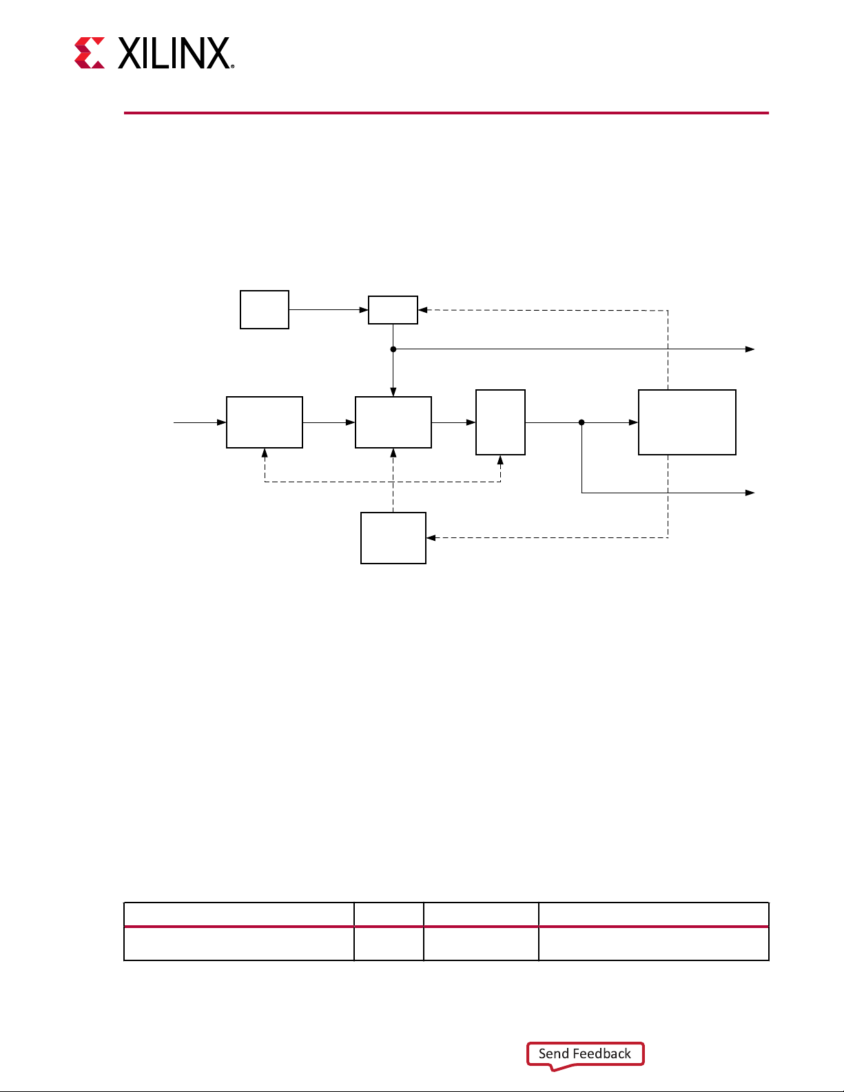
Chapter 4: Receiver
Send Feedback
RX CDR
The RX clock data recovery (CDR) circuit in each UltraScale+ FPGA GTM transceiver channel
extracts the recovered clock and data from an incoming data stream. The following gure
illustrates the architecture of the CDR block. Clock paths are shown with doed lines for clarity.
Figure 40: CDR Block Diagram
PI
Adaptation
DFE
+
FFE
Recovered
Clock
CDR FSM
RX Data
X20925-053118
RXP/N
PLL
CTLE ADC
The GTM transceiver employs the baud-rate phase detecon CDR architecture. Incoming data
rst goes through receiver equalizaon and ADC where the data is sampled. The sampled data
then moves through FFE and DFE before feeding to the CDR state machine and the downstream
transceiver blocks.
The LCPLL provides a base clock to the phase interpolator. The phase interpolator in turn
produces ne, evenly spaced sampling phases to allow the CDR state machine to have ne phase
control. The CDR state machine can track incoming data streams that can have a frequency
oset from the local PLL reference clock.
UG581 (v1.0) January 4, 2019 www.xilinx.com
Virtex UltraScale+ GTM Transceivers 93
Ports and Attributes
The following table denes the CDR ports.
Table 52:
CH[0/1]_RXCDROVRDEN In Async Reserved. Use the recommended value
CDR Ports
Port Dir Clock Domain Description
from the Wizard.
Page 94

Chapter 4: Receiver
Send Feedback
Table 52: CDR Ports (cont'd)
Port Dir Clock Domain Description
CH[0/1]_RXCDRFRRESET In Async Reserved. Use the recommended value
CH[0/1]_RXCDRHOLD In Async Hold the CDR control loop frozen.
CH[0/1]_RXCDRINCPCTRL In Async Reserved. Use the recommended value
CH[0/1]_RXCDRPHRESET In Async Reserved. Use the recommended value
CH[0/1]_RXCDRFREQOS In Async Reserved. Use the recommended value
from the Wizard.
from the Wizard.
from the Wizard.
from the Wizard.
The following table denes the CDR aributes.
Table 53: CDR Attributes
Attribute Type Description
CH[0/1]_RX_CDR_CFG0A 16-bit CDR configuration. Use the recommended value
CH[0/1]_RX_CDR_CFG0B 16-bit CDR configuration. Use the recommended value
CH[0/1]_RX_CDR_CFG1A 16-bit CDR configuration. Use the recommended value
CH[0/1]_RX_CDR_CFG1B 16-bit CDR configuration. Use the recommended value
CH[0/1]_RX_CDR_CFG2A 16-bit CDR configuration. Use the recommended value
CH[0/1]_RX_CDR_CFG2B 16-bit CDR configuration. Use the recommended value
CH[0/1]_RX_CDR_CFG3A 16-bit CDR configuration. Use the recommended value
CH[0/1]_RX_CDR_CFG3B 16-bit CDR configuration. Use the recommended value
CH[0/1]_RX_CDR_CFG4A 16-bit CDR configuration. Use the recommended value
CH[0/1]_RX_CDR_CFG4B 16-bit CDR configuration. Use the recommended value
from the Wizard.
from the Wizard.
from the Wizard.
from the Wizard.
from the Wizard.
from the Wizard.
from the Wizard.
from the Wizard.
from the Wizard.
from the Wizard.
UG581 (v1.0) January 4, 2019 www.xilinx.com
Virtex UltraScale+ GTM Transceivers 94
RX Fabric Clock Output Control
The RX Clock Divider Control block has two main components: serial clock divider control, and
parallel clock divider and selector control. The clock divider and selector details are illustrated in
the following gure.
Page 95

Figure 41: RX Serial and Parallel Clock Divider
Send Feedback
GTM_DUAL (GTM Transceiver Primitive)
Chapter 4: Receiver
TXP/N
MGTREFCLKP
MGTREFCLKN
REFCLK_HROW_CK_SEL
SIPO
ADC DSP CDR
RX CLKGEN
Phase
Interp.
LCPLL
REFCLK SEL
REFCLK Distribution
IBUFDS_GTM
RX PCSRX PMA
RX DATA
/16
Output to
GTM_DUAL
O
ODIV2
RX PROG
DIV
/2
Polarity
Control
RXRECCLK[0/1] from the other GTM RX
channel within the same GTM_DUAL
Gray
Decoder
RXRECCLK[0/1]
Pre-
Coder
Output Clock to BUFG_GT
RX DATA to Downstream
PCS Blocks
RX FIFO
CH[0/1]_RXUSRCLK
CH[0/1]_RXPROGDIVCLK
Output to
MGTREFCLK Pad
X20927-110218
Notes relevant to the gure:
1. CH[0/1]_RXPROGDIVCLK is used as the source of the interconnect logic clock via BUFG_GT.
2. There is only one LCPLL in the GTM_DUAL primive which is shared between the TX/RX.
3. RXRECCLK[0/1] is the same as CH[0/1]_RXPROGDIVCLK. It can be routed to the
MGTREFCLK output pad to be used elsewhere.
RX Programmable Divider
The RX programmable divider shown in Figure 41 uses the LCPLL output clock to generate a
parallel output clock. By using the transceiver LCPLL, RX programmable divider, and BUFG_GT,
CH[0/1]_RXPROGDIVCLK should be used as a clock source for the interconnect logic.
The following tables show the programmable divider ports and aributes, respecvely.
UG581 (v1.0) January 4, 2019 www.xilinx.com
Virtex UltraScale+ GTM Transceivers 95
Page 96

Chapter 4: Receiver
Send Feedback
Table 54: RX Programmable Divider Ports
Port Dir Clock Domain Description
CH[0/1]_RXPROGDIVRESET In Async This active-High port resets the dividers as
CH[0/1]_RXPRGDIVRESETDONE
CH[0/1]_RXPROGDIVCLK Out Clock RXPROGDIVCLK is the parallel clock output
Out Async When the input clock is stable and reset is
well as the RXPRGDIVRESETDONE
indicator. A reset must be performed
whenever the input clock source is
interrupted.
performed, this active-High signal
indicates the reset is completed and the
output clock is stable.
from The RX programmable divider. This
clock is the recommended output to the
interconnect logic through BUFG_GT.
Table 55: RX Programmable Divider Attribute
Attribute Type Description
CH[0/1]_RX_ANA_CFG1 16-bit Reserved.
Bit Name Address Description
RX_PROGDIV_SELFR [13] This attribute is used during the RX programmable
RX_PROGDIV_SEL_DIV66 [12] This attribute is used during the RX programmable
divider ratio selection. Set to 1’b1 to obtain the full
rate of the divided clock. Set to 1’b0 to obtain the
half rate of the divided clock.
divider ratio selection.
RX_PROGDIV_SEL_DIV5
• The attribute must be set to 1’b1 when the
desired divider value is either 16.5, 33, 66, or
132.
• For all other divider values, this should be set to
1’b0.
[11] This attribute is used during the RX programmable
divider ratio selection.
• The attribute must be set to 1’b0 when the
desired divider value is either 16.5, 33, 66, or
132.
• For all other divider values, this should be set to
1’b1.
UG581 (v1.0) January 4, 2019 www.xilinx.com
Virtex UltraScale+ GTM Transceivers 96
Page 97

Chapter 4: Receiver
Send Feedback
Table 55: RX Programmable Divider Attribute (cont'd)
Attribute Type Description
RX_PROGDIV_FBDIV [7:2] This attribute is the main RX programmable divider
selector.
When the following settings are set:
RX_PROGDIV_SEL_DIV66 = 1’b0
RX_PROGDIV_SEL_DIV5 = 1’b1
RX_PROGDIV_SELFR = 1’b1 (or 1’b0)
Valid RX programmable divider ratios are:
6'b011000: 4 (8)
6'b111000: 5 (10)
6'b000000: 8 (16)
6'b100000: 10 (20)
6'b000001: 12 (24)
6'b100001: 15 (30)
6'b000010: 16 (32)
6'b100010: 20 (40)
6'b000101: 24 (48)
6'b100011: 25 (50)
6'b100101: 30 (60)
6'b000110: 32 (64)
6'b100110: 40 (80)
6'b001101: 48 (96)
6'b100111: 50 (100)
6'b101101: 60 (120)
6'b001110: 64 (128)
6'b001111: 80 (160)
6'b101111: 100 (200)
UG581 (v1.0) January 4, 2019 www.xilinx.com
Virtex UltraScale+ GTM Transceivers 97
When the following settings are set:
RX_PROGDIV_SEL_DIV66 = 1’b1
RX_PROGDIV_SEL_DIV5 = 1’b0
RX_PROGDIV_SELFR = 1’b1 (or 1’b0)
Valid RX programmable divider ratios are:
6'b011000: 16.5 (33)
6'b000000: 33 (66)
6'b000010: 66 (132)
Ports and Attributes
The following table denes the ports required for TX fabric clock output control.
Page 98

Chapter 4: Receiver
Send Feedback
Table 56: RX Fabric Clock Output Control Ports
Port Dir Clock Domain Description
CH[0/1]_RXOUTCLKSEL[2:0] In Async This port must be set to 3'b000.
CH[0/1]_RXOUTCLK Out Clock Reserved.
CH[0/1]_RXPROGDIVCLK Out Clock RXPROGDIVCLK is the parallel output clock from
RXRECCLK[0/1] Out Clock RXRECCLK is the same as RXPROGDIVCLK, and it
the RX programmable divider. This clock is the
recommended output to the interconnect logic
through BUFG_GT.
can be routed to the MGTREFCLK output pad.
RX Margin Analysis
As line rates and channel aenuaon increase, the receiver equalizers are more oen enabled to
overcome channel aenuaon. This poses a challenge to system bring-up because the quality of
the link cannot be determined by measuring the far-end eye opening at the receiver pins. At high
line rates, the received eye measurement on the printed circuit board can appear to be
completely closed even though the internal eye aer the receiver equalizer is open.
Because the GTM receiver is ADC-based, the convenonal eye scan used in the previous family
of transceivers (such as GTH and GTY transceivers) is not possible. The GTM RX provides a
sampled eye diagram that can be used to measure and visualize the receiver signal margin aer
the equalizer, as shown in the following gure.
Figure 42: Sampled Eye Diagram for (a) PAM4 and (b) NRZ Modulation
UG581 (v1.0) January 4, 2019 www.xilinx.com
Virtex UltraScale+ GTM Transceivers 98
Page 99

Chapter 4: Receiver
Send Feedback
The sampled eye diagram is constructed by plong one sample per symbol located at the CDR
sampling point (aer the equalizer). By plong mulple samples, the image looks like the gure
above. Sampled eye supports both NRZ and PAM4 modulaon, with the only dierence being
that the NRZ eye consists of two amplitude margin levels, and PAM4 with four disnct amplitude
margin levels.
RX Pre-Coder
UltraScale+ GTM receiver supports pre-coding. Pre-coding can be used to reduce receiver DFE
error propagaon by reducing 1-tap burst error runs into two errors for every error event.
Ports and Attributes
The following table denes the aributes required for RX pre-coder control.
Table 57: Pre-Coder Attributes
Attribute Type Description
CH[0/1]_RX_PCS_CFG0 16-bit Reserved.
Bit Name Address Description
RX_PRECODE_ENDIAN [11] In PAM4 mode, this attribute controls pre-coder
RX_PRECODE_BYP_EN
[10] In PAM4 mode, this attribute enables pre-coding. In
received endianness. In NRZ mode, the default
Wizard value must be used.
1’b0: Non-inverting.
1’b1: Inverting.
NRZ mode, the default Wizard value must be used.
1’b0: Enables pre-code.
1’b1: Disables pre-code.
IMPORTANT! In PAM4 mode, if the pre-coder is enabled for the receiver, the transmier pre-coder
should also be enabled for proper data recovery.
UG581 (v1.0) January 4, 2019 www.xilinx.com
Virtex UltraScale+ GTM Transceivers 99
RX Gray Encoder
The UltraScale+ FPGA GTM receiver supports two types of binary enconding opons: linear and
Gray coding. By using Gray coding, only one bit error per symbol is made for incorrect decisions,
thus reducing the bit-error rate by more than 33%. Table 58 illustrates the dierences between
linear and Gray Coding.
Page 100

Chapter 4: Receiver
Send Feedback
Ports and Attributes
The following table denes the aributes required for RX Gray Encoder control.
Table 58: Gray Encoder Attributes
Attribute Type Description
CH[0/1]_RX_PCS_CFG0 16-bit Reserved.
Bit Name Address Description
RX_GRAY_ENDIAN [13] In PAM4 mode, this attribute controls the received
endianness. In NRZ mode, the default Wizard value
must be used.
1’b0: Non-inverting.
1’b1: Inverting.
RX_GRAY_BYP_EN
[12] In PAM4 mode, this attribute enables Gray
encoding. In NRZ mode, the default Wizard value
must be used.
1’b0: Enables Gray encoding.
1’b1: Disables Gray encoding.
IMPORTANT! In PAM4 mode, if the Gray Encoder is enabled for the receiver, the transmier Gray
Encoder should also be enabled for proper data recovery.
RX Polarity Control
If the RXP and RXN dierenal traces are accidentally swapped on the PCB, the dierenal data
received by the GTM RX is reversed. The GTM RX allows inversion to be done on parallel bytes
in the PCS aer the SIPO to oset reversed polarity on the dierenal pair. The polarity control
funcon uses the CH0_RXPOLARITY and CH1_RXPOLARITY input, which is driven High from
the interconnect logic interface to invert polarity.
UG581 (v1.0) January 4, 2019 www.xilinx.com
Virtex UltraScale+ GTM Transceivers 100
Ports and Attributes
The following table denes the ports required for RX polarity control.
 Loading...