

Page 1

VCU1525
Reconfigurable
Acceleration Platform
User Guide
UG1268 (v1.3) August 7, 2018
Page 2
Revision History
Send Feedback
The following table shows the revision history for this document.
Date Version Revision
08/07/2018 1.3 Revised Step 4: Program the Base Platform.
07/09/2018 1.2 Revised Board Features, Board Specifications, Table 2-1 , Installing the VCU1525 Board
in a Server Chassis, and Figure 3-11. Removed Xilinx constraints file information.
Added Appendix A, Board Installation.
04/02/2018 1.1 Revised Board Specifications and Installing the VCU1525 Board in a Server Chassis.
Updated Tab le 2 -1, Table 2 -2 , and Table 3- 9. Revised paragraph after Ta bl e 3-2.
Added Figure 3-13. Updated Figure 3-14, Figure 3-15, and Figure 3-16. Revised
Appendix B, Regulatory and Compliance Information.
11/13/2017 1.0 Initial Xilinx release.
VCU1525 Acceleration Platform User Guide 2
UG1268 (v1.3) August 7, 2018 www.xilinx.com
Page 3

Table of Contents
Send Feedback
Revision History . . . . . . . . . . . . . . . . . . . . . . . . . . . . . . . . . . . . . . . . . . . . . . . . . . . . . . . . . . . . . . . . . . . . 2
Chapter 1: Introduction
Overview . . . . . . . . . . . . . . . . . . . . . . . . . . . . . . . . . . . . . . . . . . . . . . . . . . . . . . . . . . . . . . . . . . . . . . . . 5
Block Diagram . . . . . . . . . . . . . . . . . . . . . . . . . . . . . . . . . . . . . . . . . . . . . . . . . . . . . . . . . . . . . . . . . . . . 7
Board Features . . . . . . . . . . . . . . . . . . . . . . . . . . . . . . . . . . . . . . . . . . . . . . . . . . . . . . . . . . . . . . . . . . . . 8
Board Specifications . . . . . . . . . . . . . . . . . . . . . . . . . . . . . . . . . . . . . . . . . . . . . . . . . . . . . . . . . . . . . . . 9
Dimensions . . . . . . . . . . . . . . . . . . . . . . . . . . . . . . . . . . . . . . . . . . . . . . . . . . . . . . . . . . . . . . . . . . . . . . . . . . . . . . .9
Environmental . . . . . . . . . . . . . . . . . . . . . . . . . . . . . . . . . . . . . . . . . . . . . . . . . . . . . . . . . . . . . . . . . . . . . . . . . . . . .9
Operating Voltage . . . . . . . . . . . . . . . . . . . . . . . . . . . . . . . . . . . . . . . . . . . . . . . . . . . . . . . . . . . . . . . . . . . . . . . . .10
Chapter 2: Board Setup and Configuration
Board Component Location. . . . . . . . . . . . . . . . . . . . . . . . . . . . . . . . . . . . . . . . . . . . . . . . . . . . . . . . . 11
Default Switch Settings . . . . . . . . . . . . . . . . . . . . . . . . . . . . . . . . . . . . . . . . . . . . . . . . . . . . . . . . . . . . 13
Installing the VCU1525 Board in a Server Chassis . . . . . . . . . . . . . . . . . . . . . . . . . . . . . . . . . . . . . . . . . . . . . . .13
FPGA Configuration . . . . . . . . . . . . . . . . . . . . . . . . . . . . . . . . . . . . . . . . . . . . . . . . . . . . . . . . . . . . . . . 14
Chapter 3: Board Component Descriptions
Overview . . . . . . . . . . . . . . . . . . . . . . . . . . . . . . . . . . . . . . . . . . . . . . . . . . . . . . . . . . . . . . . . . . . . . . . 16
Component Descriptions . . . . . . . . . . . . . . . . . . . . . . . . . . . . . . . . . . . . . . . . . . . . . . . . . . . . . . . . . . . 16
Virtex UltraScale+ XCVU9P-L2FSGD2104E FPGA . . . . . . . . . . . . . . . . . . . . . . . . . . . . . . . . . . . . . . . . . . . . . . . .16
I/O Voltage Rails . . . . . . . . . . . . . . . . . . . . . . . . . . . . . . . . . . . . . . . . . . . . . . . . . . . . . . . . . . . . . . . . . . . . . . . . . .16
DDR4 DIMM Memory . . . . . . . . . . . . . . . . . . . . . . . . . . . . . . . . . . . . . . . . . . . . . . . . . . . . . . . . . . . . . . . . . . . . . .18
Quad SPI Flash Memory . . . . . . . . . . . . . . . . . . . . . . . . . . . . . . . . . . . . . . . . . . . . . . . . . . . . . . . . . . . . . . . . . . . .19
USB JTAG Interface . . . . . . . . . . . . . . . . . . . . . . . . . . . . . . . . . . . . . . . . . . . . . . . . . . . . . . . . . . . . . . . . . . . . . . . .20
FT4232HQ USB-UART Interface . . . . . . . . . . . . . . . . . . . . . . . . . . . . . . . . . . . . . . . . . . . . . . . . . . . . . . . . . . . . . .21
Clock Generation . . . . . . . . . . . . . . . . . . . . . . . . . . . . . . . . . . . . . . . . . . . . . . . . . . . . . . . . . . . . . . . . . . . . . . . . . .24
System Clock and QSFP0 Clock. . . . . . . . . . . . . . . . . . . . . . . . . . . . . . . . . . . . . . . . . . . . . . . . . . . . . . . . . . . . . . .26
QSFP1 Clock . . . . . . . . . . . . . . . . . . . . . . . . . . . . . . . . . . . . . . . . . . . . . . . . . . . . . . . . . . . . . . . . . . . . . . . . . . . . . .28
Programmable MGT and User Clock . . . . . . . . . . . . . . . . . . . . . . . . . . . . . . . . . . . . . . . . . . . . . . . . . . . . . . . . . .29
GTY Transceivers . . . . . . . . . . . . . . . . . . . . . . . . . . . . . . . . . . . . . . . . . . . . . . . . . . . . . . . . . . . . . . . . . . . . . . . . . .30
PCI Express Endpoint Connectivity . . . . . . . . . . . . . . . . . . . . . . . . . . . . . . . . . . . . . . . . . . . . . . . . . . . . . . . . . . .32
28 Gb/s QSFP+ Module Connectors. . . . . . . . . . . . . . . . . . . . . . . . . . . . . . . . . . . . . . . . . . . . . . . . . . . . . . . . . . .33
I2C Bus . . . . . . . . . . . . . . . . . . . . . . . . . . . . . . . . . . . . . . . . . . . . . . . . . . . . . . . . . . . . . . . . . . . . . . . . . . . . . . . . . .34
Status LEDs . . . . . . . . . . . . . . . . . . . . . . . . . . . . . . . . . . . . . . . . . . . . . . . . . . . . . . . . . . . . . . . . . . . . . . . . . . . . . . .38
User I/O . . . . . . . . . . . . . . . . . . . . . . . . . . . . . . . . . . . . . . . . . . . . . . . . . . . . . . . . . . . . . . . . . . . . . . . . . . . . . . . . .39
Board Management Controller . . . . . . . . . . . . . . . . . . . . . . . . . . . . . . . . . . . . . . . . . . . . . . . . . . . . . . . . . . . . . .39
Board Management Controller Voltage Measurements . . . . . . . . . . . . . . . . . . . . . . . . . . . . . . . . . . . . . . .
VCU1525 Board Power System . . . . . . . . . . . . . . . . . . . . . . . . . . . . . . . . . . . . . . . . . . . . . . . . . . . . . . . . . . . . . .44
. . .43
VCU1525 Acceleration Platform User Guide 3
UG1268 (v1.3) August 7, 2018 www.xilinx.com
Page 4

Monitoring Voltage and Current . . . . . . . . . . . . . . . . . . . . . . . . . . . . . . . . . . . . . . . . . . . . . . . . . . . . . . . . . . . . .46
Send Feedback
Vccint Regulator Circuit . . . . . . . . . . . . . . . . . . . . . . . . . . . . . . . . . . . . . . . . . . . . . . . . . . . . . . . . . . . . . . . . . . . .46
Cooling Fan Connector . . . . . . . . . . . . . . . . . . . . . . . . . . . . . . . . . . . . . . . . . . . . . . . . . . . . . . . . . . . . . . . . . . . . .47
Appendix A: Board Installation
Introduction . . . . . . . . . . . . . . . . . . . . . . . . . . . . . . . . . . . . . . . . . . . . . . . . . . . . . . . . . . . . . . . . . . . . . 48
Installing a Board . . . . . . . . . . . . . . . . . . . . . . . . . . . . . . . . . . . . . . . . . . . . . . . . . . . . . . . . . . . . . . . . . 48
Step 1: Set Up the Card and Computer . . . . . . . . . . . . . . . . . . . . . . . . . . . . . . . . . . . . . . . . . . . . . . . . . . . . . . . .48
Step 2: Prepare Board Installation Files. . . . . . . . . . . . . . . . . . . . . . . . . . . . . . . . . . . . . . . . . . . . . . . . . . . . . . . .49
Step 3: Install Board Drivers . . . . . . . . . . . . . . . . . . . . . . . . . . . . . . . . . . . . . . . . . . . . . . . . . . . . . . . . . . . . . . . . .50
Step 4: Program the Base Platform . . . . . . . . . . . . . . . . . . . . . . . . . . . . . . . . . . . . . . . . . . . . . . . . . . . . . . . . . . .50
Step 5: Verify Successful Board Installation . . . . . . . . . . . . . . . . . . . . . . . . . . . . . . . . . . . . . . . . . . . . . . . . . . . .51
Debugging the Installation . . . . . . . . . . . . . . . . . . . . . . . . . . . . . . . . . . . . . . . . . . . . . . . . . . . . . . . . . 52
SDx Debug Command Options . . . . . . . . . . . . . . . . . . . . . . . . . . . . . . . . . . . . . . . . . . . . . . . . . . . . . . . . . . . . . . .53
dmatest Command . . . . . . . . . . . . . . . . . . . . . . . . . . . . . . . . . . . . . . . . . . . . . . . . . . . . . . . . . . . . . . . . . . . . . . . .54
Example Output using VCU1525 . . . . . . . . . . . . . . . . . . . . . . . . . . . . . . . . . . . . . . . . . . . . . . . . . . . . . . . . . . . . .54
Failure to Create a Compute Program . . . . . . . . . . . . . . . . . . . . . . . . . . . . . . . . . . . . . . . . . . . . . . . . . . . . . . . . .55
Useful Debug Operating System Commands . . . . . . . . . . . . . . . . . . . . . . . . . . . . . . . . . . . . . . . . . . . . . . . . . . .56
Other OS Commands. . . . . . . . . . . . . . . . . . . . . . . . . . . . . . . . . . . . . . . . . . . . . . . . . . . . . . . . . . . . . . . . . . . . . . .59
Appendix B: Regulatory and Compliance Information
Overview . . . . . . . . . . . . . . . . . . . . . . . . . . . . . . . . . . . . . . . . . . . . . . . . . . . . . . . . . . . . . . . . . . . . . . . 60
CE Directives. . . . . . . . . . . . . . . . . . . . . . . . . . . . . . . . . . . . . . . . . . . . . . . . . . . . . . . . . . . . . . . . . . . . . 60
CE Standards. . . . . . . . . . . . . . . . . . . . . . . . . . . . . . . . . . . . . . . . . . . . . . . . . . . . . . . . . . . . . . . . . . . . . 60
Electromagnetic Compatibility . . . . . . . . . . . . . . . . . . . . . . . . . . . . . . . . . . . . . . . . . . . . . . . . . . . . . . . . . . . . . . .60
Safety . . . . . . . . . . . . . . . . . . . . . . . . . . . . . . . . . . . . . . . . . . . . . . . . . . . . . . . . . . . . . . . . . . . . . . . . . . . . . . . . . . .61
Markings . . . . . . . . . . . . . . . . . . . . . . . . . . . . . . . . . . . . . . . . . . . . . . . . . . . . . . . . . . . . . . . . . . . . . . . . 61
Appendix C: Additional Resources and Legal Notices
Xilinx Resources . . . . . . . . . . . . . . . . . . . . . . . . . . . . . . . . . . . . . . . . . . . . . . . . . . . . . . . . . . . . . . . . . . 62
Documentation Navigator and Design Hubs . . . . . . . . . . . . . . . . . . . . . . . . . . . . . . . . . . . . . . . . . . . 62
References . . . . . . . . . . . . . . . . . . . . . . . . . . . . . . . . . . . . . . . . . . . . . . . . . . . . . . . . . . . . . . . . . . . . . . 63
Please Read: Important Legal Notices . . . . . . . . . . . . . . . . . . . . . . . . . . . . . . . . . . . . . . . . . . . . . . . . 64
VCU1525 Acceleration Platform User Guide 4
UG1268 (v1.3) August 7, 2018 www.xilinx.com
Page 5
Introduction
X20017-110217
Send Feedback
Overview
The VCU1525 Reconfigurable Acceleration Platform is a peripheral component interconnect
express (PCIe®) Gen3 x16 compliant board featuring the Xilinx® Virtex® UltraScale+™
XCVU9P-L2FSGD2104E FPGA. This Xilinx FPGA-based PCIe accelerator board is designed to
accelerate compute-intensive applications like machine learning, data analytics, and video
processing.
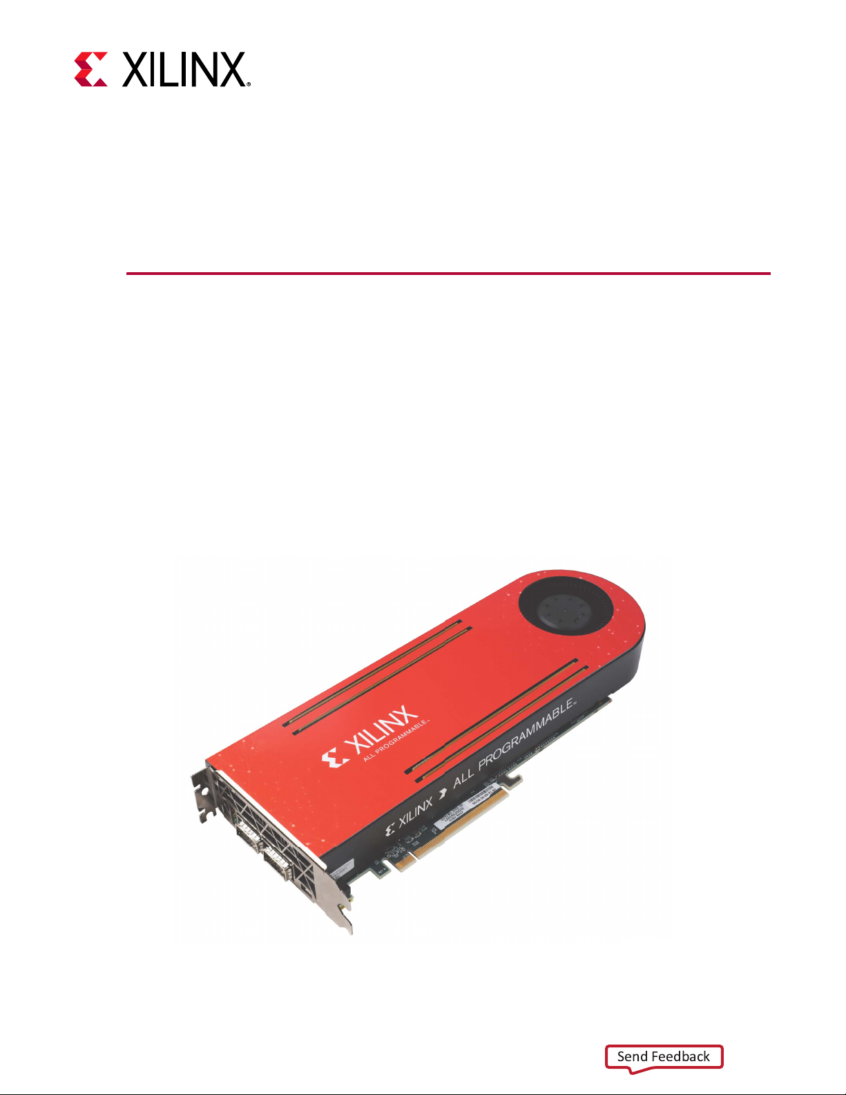
The VCU1525 board is available in both active and passive cooling configurations and
designed to be used in cloud data center servers.
Figure 1-1 shows the VCU1525 active cooling configuration (PC applications).
Chapter 1
X-Ref Target - Figure 1-1
VCU1525 Acceleration Platform User Guide 5
UG1268 (v1.3) August 7, 2018 www.xilinx.com
Figure 1-1: VCU1525 Reconfigurable Acceleration Platform (Active Cooling)
Page 6
X-Ref Target - Figure 1-2
X20018-110217
Send Feedback
Chapter 1: Introduction
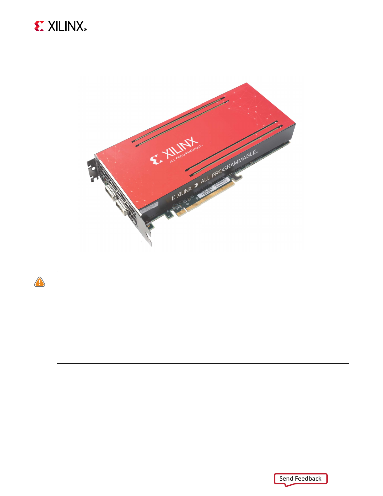
Figure 1-2 shows the VCU1525 passive cooling configuration (data center server
applications).
Figure 1-2: VCU1525 Reconfigurable Acceleration Platform (Passive Cooling)
CAUTION! The VCU1525 board with passive cooling is designed to be installed into a data center
server, where controlled air flow provides direct cooling. The VCU1525 board with active cooling is
designed to be installed into a PC environment where the air flow is uncontrolled, hence this
configuration has the heat sink and fan enclosure cover installed to provide appropriate cooling. In
either cooling configuration, due to the board enclosure, switches are not accessible, nor are LEDs
visible (except the triple-LED module DS3 which protrudes through the left front end PCIe bracket).
Board details revealed in this user guide are provided to aid understanding of board features. If the
cooling enclosure is removed from either configuration of the board and it is powered-up, external fan
cooling airflow MUST be applied to prevent over-temperature shut-down and possible damage to the
board electronics.
See Appendix C, Additional Resources and Legal Notices for references to documents, files,
and resources relevant to the VCU1525 board.
VCU1525 Acceleration Platform User Guide 6
UG1268 (v1.3) August 7, 2018 www.xilinx.com
Page 7
X-Ref Target - Figure 1-3
244-pin DIMM interface
64-bit + ECC dual rank support
x4/x8 UDIMM support
PC4-2400 compatible
C0
244-pin DIMM interface
64-bit + ECC dual rank support
x4/x8 UDIMM support
PC4-2400 compatible
C2
244-pin DIMM interface
64-bit + ECC dual rank support
x4/x8 UDIMM support
PC4-2400 compatible
C3
244-pin DIMM interface
64-bit + ECC dual rank support
x4/x8 UDIMM support
PC4-2400 compatible
C1
DIP SW POWER
QSPI1
QSPI2
PCIe GEN1/2/3 x 1/2/4/8/16
PCIe GEN4 x 8
QSFP #2
QSFP #1
XADC
LEDs
Clocks
VU9P
D2104
X19964-110617
Send Feedback
Chapter 1: Introduction
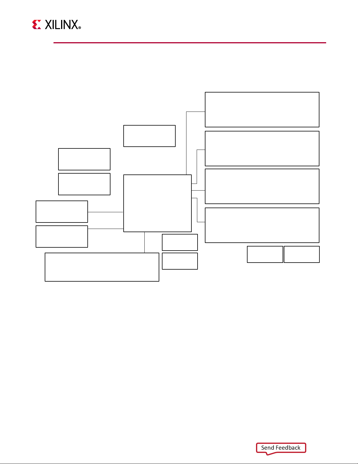
Block Diagram
A block diagram of the VCU1525 board is shown in Figure 1-3.
VCU1525 Acceleration Platform User Guide 7
UG1268 (v1.3) August 7, 2018 www.xilinx.com
Figure 1-3: VCU1525 Board Block Diagram
Page 8

Chapter 1: Introduction
Send Feedback
Board Features
The VCU1525 board features are listed in this section. Detailed information for each feature
is provided in Component Descriptions in Chapter 3.
• Virtex UltraScale+ XCVU9P-L2FSGD2104E FPGA
• Memory (four independent dual-rank DDR4 interfaces)
48 gigabyte (GB) DDR4 memory
°
4x DDR4 16 GB, 2400 mega-transfers per second (MT/s), 64-bit with error correcting
°
code (ECC) DIMM
x4/x8 unregistered dual inline memory module (UDIMM) support
°
• Configuration options
1 gigabit (Gb) Quad Serial Peripheral Interface (SPI) flash memory
°
Micro-AB universal serial bus (USB) J13 JTAG configuration port (FT4232HQ U65
°
bridge)
• 76 GTY transceivers (19 Quads)
16-lane PCI Express (16 GTY)
°
Two QSFP28 100G interfaces (8 GTY)
°
52 GTY not used
°
•Clock sources
Two Si5335A Quad clock generators
°
Si570 I2C programmable LVDS clock generator
°
• USB-to-UART FT4232HQ bridge with Micro-AB USB connector
• PCIe integrated Endpoint block connectivity
Gen1, 2 or 3 x1/x2/x4/x8/x16
°
Gen4 x8
°
•I2C bus
• Status LEDs
• User I/O (4-pole user dual-inline package (DIP) SW3, CPU_RESET PB SW1)
VCU1525 Acceleration Platform User Guide 8
UG1268 (v1.3) August 7, 2018 www.xilinx.com
• Power management with system management bus (SMBus) voltage, current, and
temperature monitoring
• Dynamic power sourcing based on external power supplied
• 75W PCIe slot functional with 35 A max V
current PCIe slot power only
CCINT
Page 9

Chapter 1: Introduction
Send Feedback
• 150 W PCIe slot functional with 110 A max V
PCIe Aux power cable connected
• 225 W PCIe slot functional with 160 A max V
PCIe Aux power cable connected
• Two QSFP28 100G interfaces
• Onboard reprogrammable flash configuration memory
• Front panel JTAG and universal asynchronous receiver-transmitter (UART) access
through the USB port
• FPGA configurable over USB/JTAG and Quad SPI configuration flash memory
• Thermal management with variable rate fan for minimal fan noise
current PCIe slot power and 6-pin
CCINT
current PCIe slot power and 8-pin
CCINT
Board Specifications
Dimensions
Height: 4.2 inch (10.67 cm)
PCB thickness (±5%): 0.062 inch (0.157 cm)
Board length, passive heat sink: 9.2 inch (23.4 cm)
Board length, active heat sink: 11.4 inch (29 cm)
Board thickness with heat sink enclosure installed:
Active: 1.52 inch (3.86 cm)
Passive: 1.44 inch (3.66 cm)
Dual slot PCIe full-length, full height form-factor compliant
Note:
A 3D model of this board is not available.
Environmental
Temperature
Operating: 0°C to +45°C
Storage: –25°C to +60°C
VCU1525 Acceleration Platform User Guide 9
UG1268 (v1.3) August 7, 2018 www.xilinx.com
Page 10

Humidity
Send Feedback
10% to 90% non-condensing
Operating Voltage
Chapter 1: Introduction
PCIe slot +12 VDC, +3.3 VDC, +3.3 V
, External +12 V
AUXDC
DC
VCU1525 Acceleration Platform User Guide 10
UG1268 (v1.3) August 7, 2018 www.xilinx.com
Page 11
Board Setup and Configuration
00
Round callout references a component
on the front side of the board
Square callout references a component
on the back side of the board
00
1
2
3
4
5
16
17
8
9
19 20
18
13
14
7
12
12
6
15
X19972-031618
Send Feedback
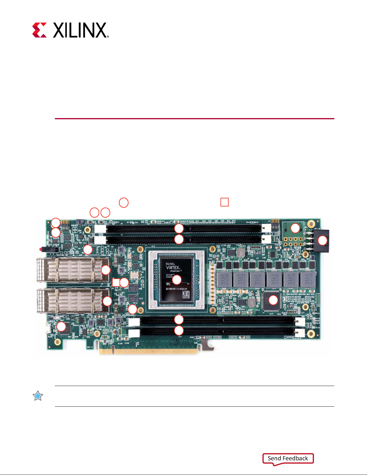
Board Component Location
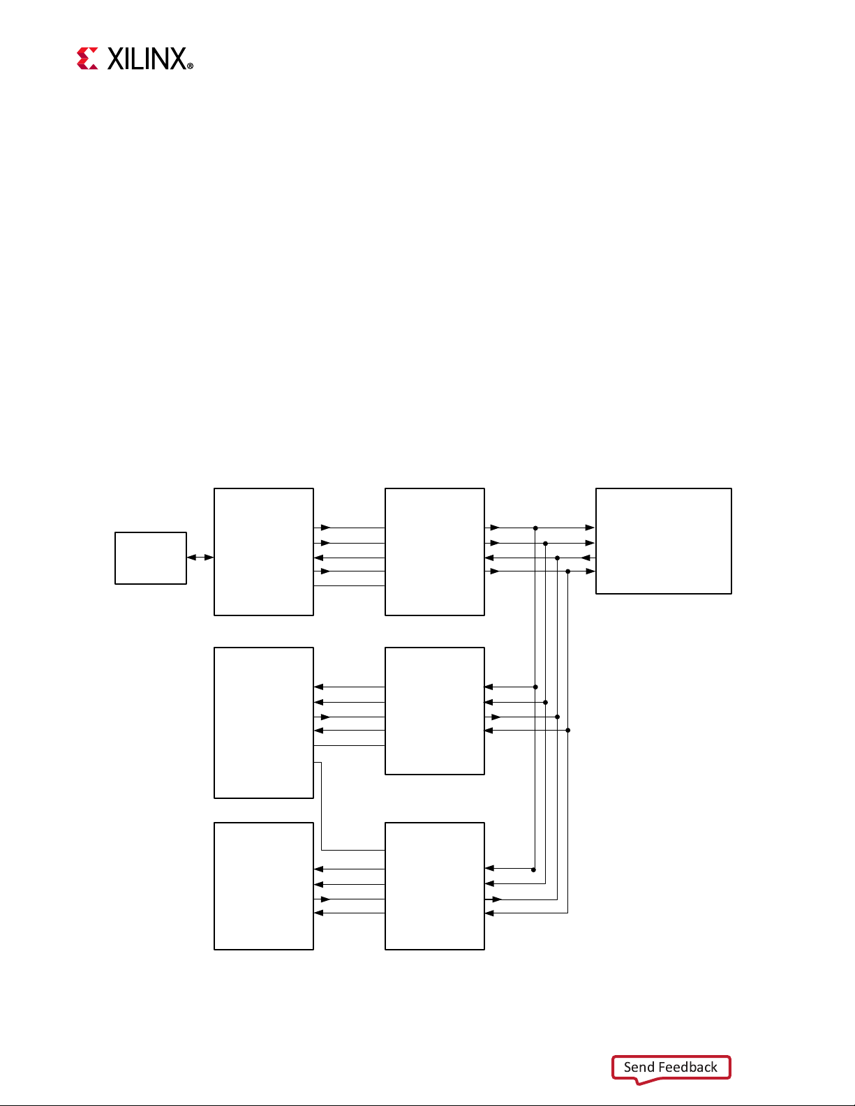
Figure 2-1 shows the location of components on the VCU1525 board. Each component
shown is keyed to Tab le 2- 1 . Ta ble 2- 1 identifies the components, references the respective
schematic page numbers, and links to a detailed functional description of the component
and board features in Chapter 3, Board Component Descriptions.
X-Ref Target - Figure 2-1
Chapter 2
VCU1525 Acceleration Platform User Guide 11
UG1268 (v1.3) August 7, 2018 www.xilinx.com
IMPORTANT: Figure 2-1 is for visual reference only and might not reflect the current revision of the
Figure 2-1: VCU1525 Board Components
board.
Page 12
CAUTION! The VCU1525 board can be damaged by electrostatic discharge (ESD). Follow standard ESD
Send Feedback
prevention measures when handling the board.
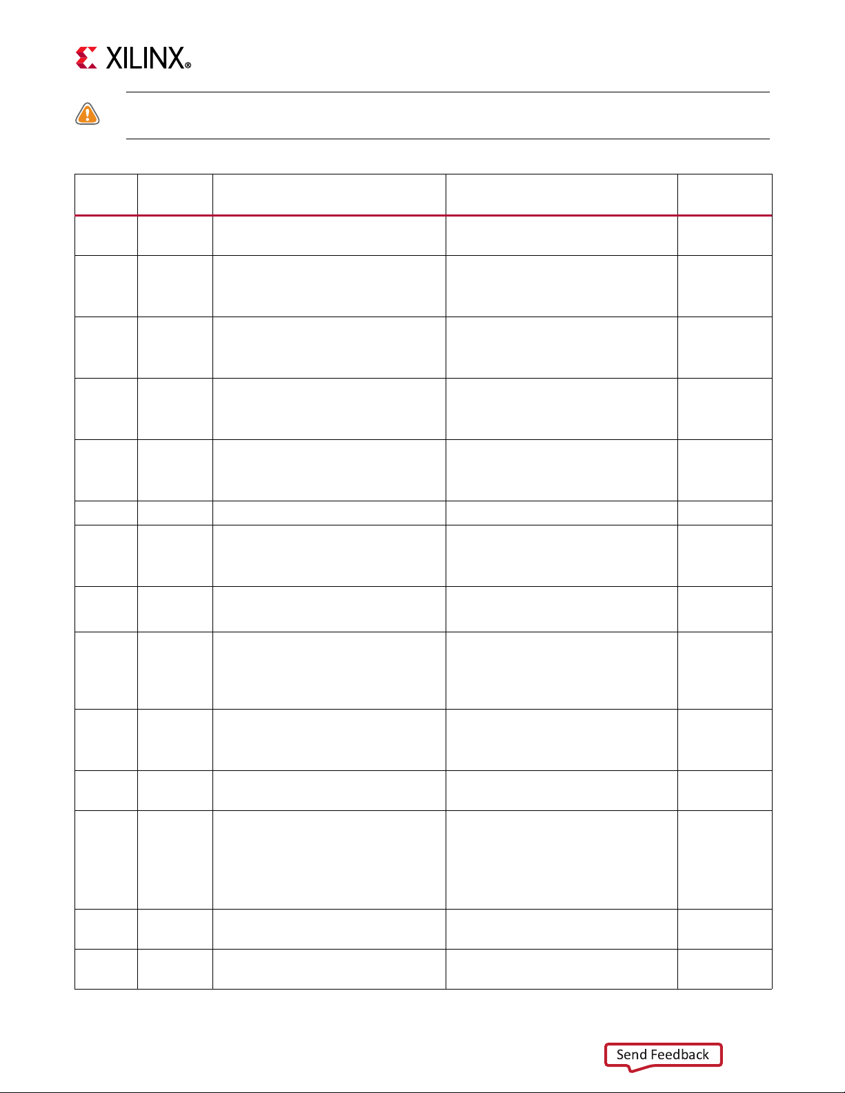
Table 2-1: VCU1525 Board Component Descriptions
Chapter 2: Board Setup and Configuration
Number Ref. Des.
1U13Virtex UltraScale+
XCVU9P-L2FSGD2104E FPGA
2 J14 C0 DDR4 72-bit DIMM memory
(16 GB)
(DDR4 DIMM Memory)
3 J12 C1 DDR4 72-bit DIMM memory
(16 GB)
(DDR4 DIMM Memory)
4 J5 C2 DDR4 72-bit DIMM memory
(16 GB)
(DDR4 DIMM Memory)
5 J2 C3 DDR4 72-bit DIMM memory
(16 GB)
(DDR4 DIMM Memory)
6 U17, U58 Quad SPI Flash Memory (1Gb total) Micron MT25QU01GBBA8E12-0SIT 12
7 U27, J13 USB JTAG bridge w/ USB Micro-AB
connector
(FT4232HQ USB-UART Interface)
Feature
(Link)
Notes
XCVU9P-L2FSGD2104E —
Micron MTA18ASF2G72PZ-2G3B1IG 33
Micron MTA18ASF2G72PZ-2G3B1IG 34
Micron MTA18ASF2G72PZ-2G3B1IG 35
Micron MTA18ASF2G72PZ-2G3B1IG 36
FTDI FT4232HQ-REEL
HIROSE ZX62D-AB-5P8
Schematic
Page
31
8 J1 SMBUS 2X5 1.27mm pitch connector
(Monitoring Voltage and Current)
9 J3 BMC CTLR. JTAG 2 X 5 1.27 mm pitch
connector
(Figure 3-18 U19 MSP432 I2C
Connectivity)
10 U9 SYSCLK_300 300MHz, QSFP0_CLOCK
156.25MHz, 1.8V LVDS
(System Clock and QSFP0 Clock)
11 U12 QSFP1_CLOCK 156.25MHz, 1.8V
LVDS (QSFP1 Clock)
12 U14, U43 USER_SI570_CLOCK, 156.25MHz,
3.3V LVDS
+1 to 4 clock buffer
(Programmable MGT and User
Clock)
13 J7 QSFP0 (28 Gb/s QSFP+ Module
Connectors)
14 J9 QSFP1 (28 Gb/s QSFP+ Module
Connectors)
SAMTEC FTSH-105-01-F-D-K 16
SAMTEC FTSH-105-01-F-D-K 24
SI5335A-B06201-GM 23
SI5335A-B06201-GM 27
Silicon Labs SI570BAB000544DG
Silicon Labs SI53340-B-GM
AMPHENOL FS1-Z38-20Z6-60 23
AMPHENOL FS1-Z38-20Z6-60 27
23
VCU1525 Acceleration Platform User Guide 12
UG1268 (v1.3) August 7, 2018 www.xilinx.com
Page 13
Table 2-1: VCU1525 Board Component Descriptions (Cont’d)
Send Feedback
Chapter 2: Board Setup and Configuration
Number Ref. Des.
15 U19 Board Management Controller
(BMC)
16 JP1 Auxiliary 12V power connector
(Vccint Regulator Circuit)
17 J4 Cooling Fan Connector JST SALES S4B-PH-K-S(LF)(SN) 11
Feature
(Link)
Notes
TI MSP432P401RIPZ 24
LIGHT JIE AARRA001-08MTTRH 17
Default Switch Settings
Default switch settings are listed in Tab l e 2 -2. Switch locations are shown in Figure 2-1.
Table 2-2: Default Switch Settings
Switch Function Default Comments Figure 2-1 Callout Schematic Page
SW3 4-pole GPIO DIP ON, ON, ON, ON 4-pole user DIP 18 11
Tab le 2 -3 shows other visible switch locations.
Table 2-3: Other Visible Switches
Schematic
Page
Component Function Comments Figure 2-1 Callout Schematic Page
SW1 Pushbutton switch CPU_RESET_B 19 11
SW2 Pushbutton switch PROGRAM_B 20 11
Installing the VCU1525 Board in a Server Chassis
Because each server or PC vendors hardware is different, for physical card installation
guidance, see the manufacturer’s PCIe card installation instructions.
For programming and start-up details, see Appendix A, Board Installation.
VCU1525 Acceleration Platform User Guide 13
UG1268 (v1.3) August 7, 2018 www.xilinx.com
Page 14
Chapter 2: Board Setup and Configuration
Send Feedback
FPGA Configuration
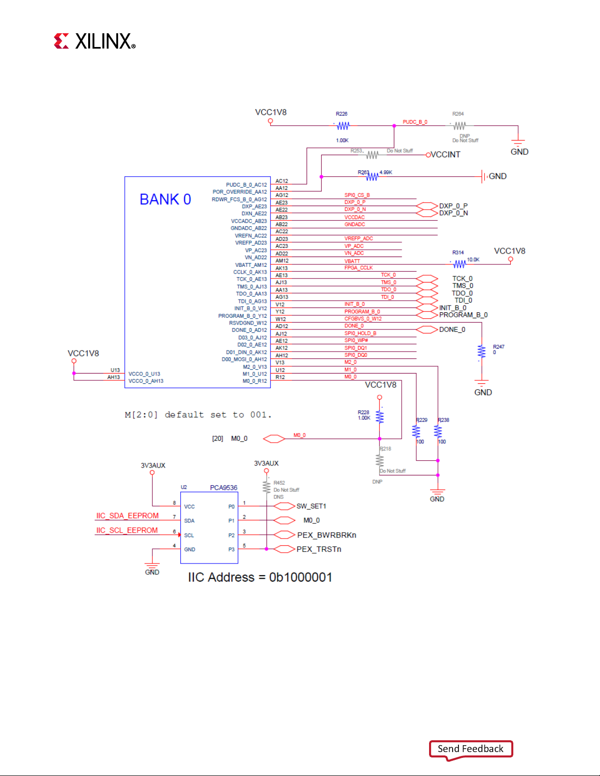
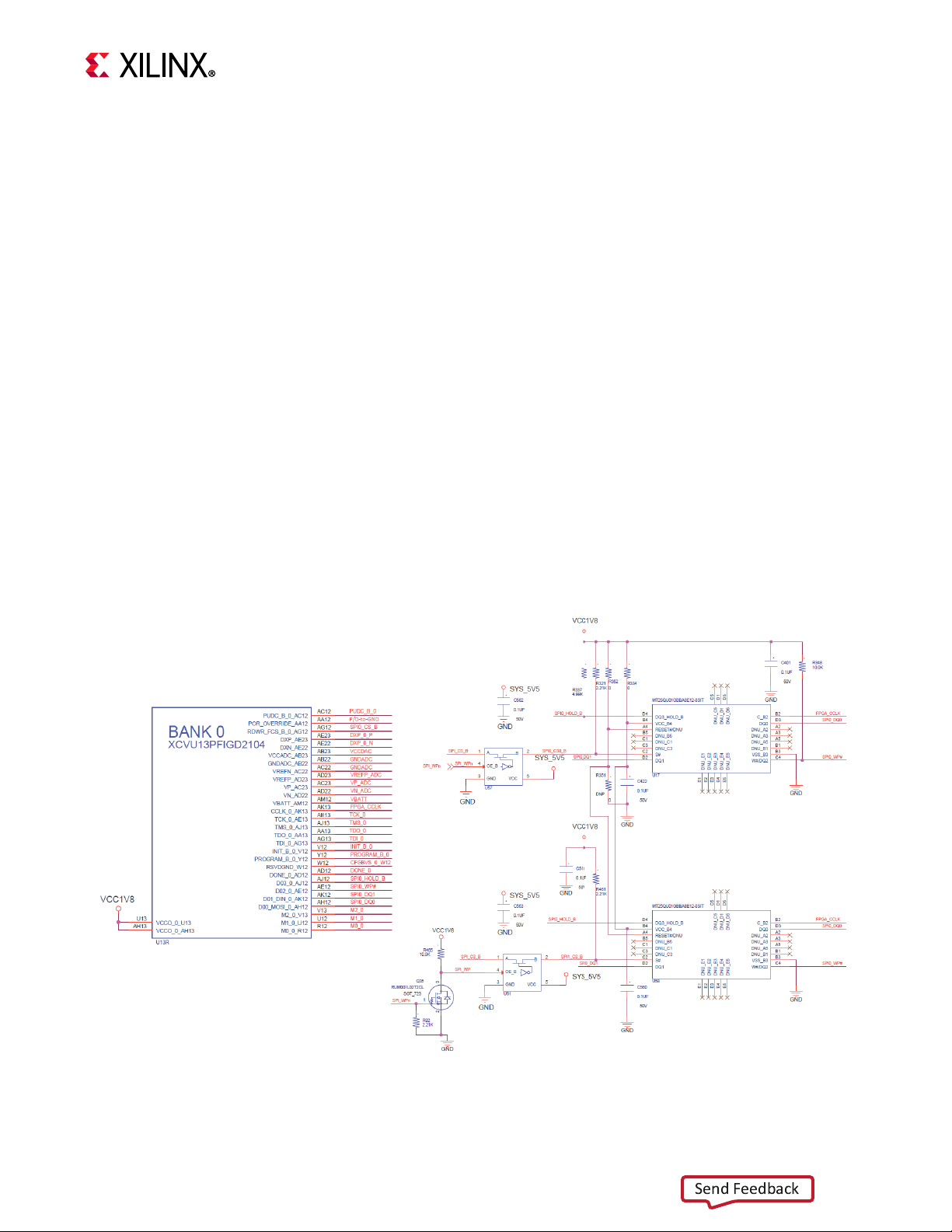
The VCU1525 board supports two UltraScale+ FPGA configuration modes:
• Quad SPI flash memory
• JTAG using USB JTAG configuration port (USB J13/FT4232H U27)
The FPGA bank 0 mode pins are hardwired to M[2:0] = 001 Master SPI mode with
pull-up/down resistors.
At power up, the FPGA is configured by the Quad SPI NOR Flash U17 device (Micron
MT25QU01GBBA8E12-0SIT) with the FPGA_CCLK operating at clock rate of 105 MHz
(EMCCLK) using the Master Serial Configuration mode.
The Quad SPI flash memory NOR device has a capacity of 1 Gb.
While the FPGA default mode selects Quad SPI configuration, JTAG mode overrides it if
invoked. JTAG mode is always available independent of the Mode pin settings.
M0 is pulled up, however it is also connected to the I2C I/O port U2 PCA9536 device (port
P1, pin 2 ). This con nection al lows M0 to b e driven lo w by the MSP432 U19 BMC over I2C (via
the I2C PCS9536 U2 port expander), disabling the Master SPI mode.
For complete details on configuring the FPGA, see UltraScale Architecture Configuration
User Guide (UG570) [Ref 1].
Table 2-4: Configuration Modes
Configuration Mode M[2:0] Bus Width CCLKL Direction
Master SPI 001 x1, x2, x4 FPGA output
JTAG Not applicable - JTAG overrides x1 Not applicable
VCU1525 Acceleration Platform User Guide 14
UG1268 (v1.3) August 7, 2018 www.xilinx.com
Page 15
X-Ref Target - Figure 2-2
X19973-103017
Send Feedback
Chapter 2: Board Setup and Configuration
The configuration circuit is shown in Figure 2-2.
VCU1525 Acceleration Platform User Guide 15
UG1268 (v1.3) August 7, 2018 www.xilinx.com
Figure 2-2: VCU1525 Configuration Circuit
Page 16
Board Component Descriptions
Send Feedback
Overview
This chapter provides a detailed functional description of board components and features.
Tab le 2 -1 identifies the components, references the respective schematic page numbers,
and links to the corresponding detailed functional description in this chapter. Component
locations are shown in Tab le 2 -1.
Component Descriptions
Chapter 3
Virtex UltraScale+ XCVU9P-L2FSGD2104E FPGA
[Figure 2-1, callout 1]
The VCU1525 board is populated with the Virtex® UltraScale+™ XCVU9P-L2FSGD2104E
FPGA.
For more information on Virtex UltraScale+ FPGAs, see Virtex UltraScale+ FPGA Data Sheet:
DC and AC Switching Characteristics (DS923) [Ref 2].
I/O Voltage Rails
There are 13 I/O banks available on the XCVU9P-L2FSGD2104E FPGA and the VCU1525
board.
VCU1525 Acceleration Platform User Guide 16
UG1268 (v1.3) August 7, 2018 www.xilinx.com
Page 17
X-Ref Target - Figure 3-1
MGTY233
MGTY232
MGTY231
MGTY230
MGTY229
MGTY228
MGTY227
MGTY226
MGTY225
MGTY224
MGTY133
MGTY131
MGTY130
MGTY129
MGTY128
MGTY123
MGTY122
MGTY121
MGTY120
72 73 74 71 70 69
66 64 65 61 62 63
67
X19971-103017
Send Feedback
Chapter 3: Board Component Descriptions
Figure 3-1 shows the XCVU9P-L2FSGD2104E bank arrangement.
Figure 3-1: XCVU9P-L2FSGD2104E Bank Arrangement
VCU1525 Acceleration Platform User Guide 17
UG1268 (v1.3) August 7, 2018 www.xilinx.com
Page 18
Chapter 3: Board Component Descriptions
Send Feedback
The voltages applied to the XCVU9P-L2FSGD2104E U13 FPGA I/O banks are listed in
Tab le 3 -1.
Table 3-1: I/O Bank Voltage Rails
XCVU9P-L2FSGD2104E Power Net Name Voltage Connected To
Bank 61 VCC1V2_BTM 1.2V DDR4 C0 DQ[0:15], DQ[40:55]
Bank 62 VCC1V2_BTM 1.2V DDR4 C0 DQ[16:39], DQ[56:63]
Bank 63 VCC1V2_BTM 1.2V DDR4 C0 DQ[64:71], ADDR/CTRL
Bank 64 VCC1V2_BTM 1.2V USB, QSFP0,QSFP1, I2C, GPIO_MSP, SW_DP
Bank 65 VCC1V2_BTM 1.2V DDR4 C1 DQ[64:71], ADDR/CTRL
Bank 66 VCC1V2_BTM 1.2V DDR4 C1 DQ[32:63]
Bank 67 VCC1V8_BTM 1.2V DDR4 C1 DQ[0:31]
Bank 69 VCC1V2_TOP 1.2V DDR4_C2 DQ[32:71]
Bank 70 VCC1V2_TOP 1.2V DDR4 C2 DQ[40:47], ADDR/CTRL
Bank 71 VCC1V2_TOP 1.2V DDR4_C2 DQ[0:31
Bank 72 VCC1V2_TOP 1.2V DDR4 C3 DQ[64:71], ADDR/CTRL
Bank 73 VCC1V2_TOP 1.2V DDR4_C3 DQ[16:31], DQ[40:55]
Bank 74 VCC1V2_TOP 1.2V DDR4_C3 DQ[0:15], DQ[32:39], DQ[56:63]
DDR4 DIMM Memory
[Figure 2-1, callout 2, 3, 4, 5]
Four independent dual-rank DDR4 interfaces are available on the VCU1525 board. The
VCU1525 board is populated with four socketed single-rank Micron
MTA18ASF2G72PZ-2G3B1IG or Samsung M393A2K40BB1-CRC 16GB DDR4 UDIMMs. Each
DDR4 is 72-bits wide (64-bits plus support for ECC).
Memory interface-to-FPGA bank assignment is shown in Ta ble 3- 1. The DDR4 0.6V V
termination voltages are sourced from four independent TI TPS51200DR regulator circuits.
The VCU1525 DDR4 memory interfaces adhere to the constraints guidelines documented in
the "DDR3/DDR4 Design Guidelines" section of the UltraScale Architecture-Based FPGAs
Memory IP LogiCORE IP Product Guide (PG150) [Ref 3]. The VCU1525 board DDR4 memory
interfaces are 40 Ω impedance implementations.
For more details about the Micron DDR4 DIMM, see the Micron MTA18ASF2G72PZ-2G3B1IG
data sheet at the Micron website [Ref 7].
TT
VCU1525 Acceleration Platform User Guide 18
UG1268 (v1.3) August 7, 2018 www.xilinx.com
For more details about the Samsung DDR4 DIMM, see the Samsung M393A2K40BB1-CRC
data sheet at the Samsung website [Ref 8].
Page 19
Chapter 3: Board Component Descriptions
X20038-110617
Send Feedback
Quad SPI Flash Memory
[Figure 2-1, callout 6]
Two Quad Serial Peripheral Interface (SPI) flash memory devices of the same type and wired
in parallel are provided on the VCU1525 board (U17 and U58). A field effect transistor (FET)
switch structure (U57 and U61) implements a chip-select enable mechanism, controlled by
the MSP432 board management controller (BMC). Only one Quad SPI device can be
enabled at a time.
The default selected (bank 0 configuration) Quad SPI flash memory is U17. Each Quad SPI
device provides 1 Gb of nonvolatile storage.
• Part number: MT25QU01GBB8E12-0SIT (Micron)
• Supply voltage: 1.8V
• Datapath width: 4 bits
• Data rate: variable
X-Ref Target - Figure 3-2
Figure 3-2 shows the linear Quad SPI flash memory circuitry on the VCU1525 board. For
more flash memory details, see the Micron MT25QU01GBB8E12-0SIT data sheet at the
Micron website [Ref 7].
VCU1525 Acceleration Platform User Guide 19
UG1268 (v1.3) August 7, 2018 www.xilinx.com
Figure 3-2: Quad SPI 1Gb Flash Memory
Page 20
X-Ref Target - Figure 3-3
FT4232HQ
USB AB
J13
U27
ADBUS0
ADBUS1
ADBUS2
ADBUS3
ADBUS5
TXBN0304
U35
B1
B3
B2
B4
A1
A3
A2
A4
OE_B
3.3V L/S 1.8V
FT TCK
FT TDO
FT TDI
FT TMS
FT OE
XCVU9PFSGD2104
U13R
TCK
TDI
TDO
TMS
BANK 0
TCK
TDI
TDO
TMS
MSP432
U19
P3_0
P3_1
P3_2
P3_3
P3_4
TXBN0304
U33
B1
B3
B2
B4
A1
A3
A2
A4
OE_B
3.3V L/S 1.8V
MSP TCK
MSP TDI
MSP TDO
MSP TMS
MSP EN
PCIe EDGE
CN1
A5
A6
A7
A8
TXBN0304
U34
B1
B3
B2
B4
A1
A3
A2
A4
OE_B
3.3V L/S 1.8V
PEX TCK
PEX TDI
PEX TDO
PEX TMS
P10_4
BD. MGMT.
CONTROLLER
PEX OE
TCK
TDI
TDO
TMS
GPIO
PORT
TCK
TDI
TDO
TMS
X19965-031418
Send Feedback
Chapter 3: Board Component Descriptions
For details on bank 0 pins, see UltraScale Architecture Configuration User Guide (UG570)
[Ref 1].
USB JTAG Interface
[Figure 2-1, callout 7]
The VCU1525 board XCVU9P-L2FSGD2104E FPGA U13 is the only component in the Joint
Test Action Group (JTAG) chain. JTAG configuration is available through the USB-to-JTAG
FTDI FT4232HQ U27 bridge device connected to Micro-AB USB connector J13. The FTDI
JTAG signals are level-shifted through TXBN0304 device U35. The PCIe 16-lane edge
connector CN1 JTAG port is connected in parallel through level-shifter U34. GPIO port 3 of
the U19 MSP432 BMC is also connected through level-shifter U33. Each level-shifter enable
pin is controlled by the BMC to allow only one JTAG connection at a time.
JTAG configuration is allowed at any time regardless of the FPGA mode pin settings.
The JTAG chain block diagram is shown in Figure 3-3.
VCU1525 Acceleration Platform User Guide 20
UG1268 (v1.3) August 7, 2018 www.xilinx.com
Figure 3-3: VCU1525 JTAG Chain Block Diagram
Page 21

Chapter 3: Board Component Descriptions
Send Feedback
For more details about the FT4232HQ device, see the FTDI website [Ref 9].
FT4232HQ USB-UART Interface
[Figure 2-1, callout 7]
The FT4232HQ U27 Quad USB-UART on the VCU1525 board provides two UART connections
through the single Micro-AB USB connector J13.
• Channel AD is configured to support the JTAG chain.
• Channel AC implements a 2-wire TX/RX UART connection to the MSP432 BMC U19.
• Channel BD implements a 2-wire level-shifted TX/RX UART connection to the XVU9P
U13.
• Channel BC is not used.
The USB UART interface circuit is shown in Figure 3-4. For finer details see the VCU1525
schematic 0381795, page 31 [Ref 10].
VCU1525 Acceleration Platform User Guide 21
UG1268 (v1.3) August 7, 2018 www.xilinx.com
Page 22

X-Ref Target - Figure 3-4
X20019-110217
Send Feedback
Chapter 3: Board Component Descriptions
Figure 3-4: Quad USB-UART Interface
The channel BD UART connection from XCVU9P-L2FSGD2104E U13 bank 64 to the
FT4232HQ U27 device is level-shifted via Q36 (TX) and Q37 (RX).
Tab le 3 -2 shows the two UART channel connections between FT4232HQ U27 and
XCVU9P-L2FSGD2104E U13 and MSP432 U19.
Table 3-2: VCU1525 USB Switch Circuit Connections
FT4232HQ U27
Target Pin Net Name
Pin Name Pin
U13.BB20 USB_UART_RX BDBUS1 39
U13.BF18 USB_UART_TX BDBUS0 38
U19.7 FT2232H_UART_RX ACBUS1 27
U19.6 FT2232H_UART_TX ACBUS0 26
VCU1525 Acceleration Platform User Guide 22
UG1268 (v1.3) August 7, 2018 www.xilinx.com
Page 23

X-Ref Target - Figure 3-5
X20020-110217
Send Feedback
Chapter 3: Board Component Descriptions
The VCU1525 board hosts a second USB connector. J17 is a keyed 1.2 mm right-angle
receptacle (Amphenol 10125839-04RAEHLF). J17 is selectable via TI TS3USB221RSER 1-to-2
USB switch U59, which is controlled by the MSP432 U19 BMC. USB switch U59 selects
between the Micro-AB USB connector J13 (port 1) and the J17 4-pin receptacle (port 2). J13
is selected by default at VCU1525 power on. The USB switch circuit is shown in Figure 3-5.
Figure 3-5: USB-UART Interface
Tab le 3 -3 lists the USB switch circuit connections.
Table 3-3: VCU1525 USB Switch Circuit Connections
TS3USB221RSER U59
Pin Pin Name Pin Name
1 1D+ USB1_DP J13.3 D_P USB J13 DP
2 1D- USB1_DN J13.2 D_N USB J13 DN
3 2D+ USB2_DP J17.2 2 USB J17 DP
4 2D- USB2_DN J17.3 3 USB J17 DN
6 OE_B USB_EN_B U19.52 P9_0 U59 USB Switch ENABLE_B
7 D- USB_DN U27.7 DM FT4232HQ U27 DN
8 D+ USB_DP U27.8 DP FT4232HQ U27 DP
9 S USB_SEL U19.53 P9_1 U59 USB Switch Port Select
J17 USB_VBUS2 present USB_PRES U19.24 P10_4 USB J17 pin 1 voltage detection
Schematic
Net Name
Connected To
Description
The FTDI FT4232HQ data sheet is available on the FTDI website [Ref 9].
VCU1525 Acceleration Platform User Guide 23
UG1268 (v1.3) August 7, 2018 www.xilinx.com
Page 24

Chapter 3: Board Component Descriptions
Send Feedback
The TS3USB221RSER data sheet is available on the TI website [Ref 11].
Clock Generation
[Figure 2-1, callout 10, 11, 12]
The VCU1525 board provides eight clock sources to the XCVU9P-L2FSGD2104E device,
listed in Tab l e 3 -4.
Table 3-4: VCU1525 Board Clock Sources
Clock Name Clock Ref. Des. Description
SYSCLK_300 clock buffer U44 source is SI5335A-B06201-GM U9 output CLK0 (300MHz).
DDR4 C0 I/F 300MHz U44 (Q0) Silicon Labs Si53340 3.3V LVDS clock buffer. SYSCLK0_300_P/N
DDR4 C0 I/F bank 63.
DDR4 C1 I/F 300MHz U44 (Q1) Silicon Labs Si53340 3.3V LVDS clock buffer. SYSCLK1_300_P/N
GPIO I/F bank 64.
DDR4 C2 I/F 300MHz U44 (Q2) Silicon Labs Si53340 3.3V LVDS clock buffer. SYSCLK2_300_P/N
DDR4 C2 I/F bank 70.
DDR4 C3 I/F 300MHz U44 (Q3) Silicon Labs Si53340 3.3V LVDS clock buffer. SYSCLK3_300_P/N
DDR4 C3 I/F bank 72.
QSFP0 CLOCK 156.250MHz U9 (CLK1) Silicon Labs Si5335A 1.8 LVDS QSFP0_CLOCK_P/N QSFP0
GTY231 REFCLK1
QSFP1 CLOCK 156.250MHz U12 (CLK1) Silicon Labs Si5335A 1.8 LVDS QSFP1_CLOCK_P/N QSFP1
GTY230 REFCLK1
USER/MGT_SI570_CLOCK buffer U43 source is SI570 U14 (156.250MHz default).
USER_SI570_CLOCK U43 (Q0) Silicon Labs Si53340 3.3V LVDS clock buffer.
USER_SI570_CLOCK_P/N GPIO I/F bank 64.
MGT SI570 CLOCK0 (QSFP0) U43 (Q2) Silicon Labs Si53340 3.3V LVDS clock buffer.
USER_SI570_CLOCK0_P/N QSFP0 GTY231 REFCLK0.
MGT SI570 CLOCK1 (QSFP1) U43 (Q3) Silicon Labs Si53340 3.3V LVDS clock buffer.
USER_SI570_CLOCK0_P/N QSFP1 GTY230 REFCLK0.
PEX_REFCLK (PCIe input) CN1 PCIe edge conn. CN1 input clock 100MHz PEX_REFCLK_P/N
GTY226 REFCLK0.
VCU1525 Acceleration Platform User Guide 24
UG1268 (v1.3) August 7, 2018 www.xilinx.com
Page 25

X-Ref Target - Figure 3-6
U9
U44
BANK 63
DDR4 C0 I/F
AY37/AY38 GC QBC
U13AF
XCVU9PFSGD2104
CLK0
Q0
Q1
Q2
Q3
SYSCLK0_300_/P/N
SYSCLK1_300_P/N
SYSCLK2_300_P/N
SYSCLK3_300_P/N
CLK0
CLK1
CLK2
CLK3
300 MHz
156.25 MHz
90 MHz
33.33 MHz
Si5335A-B06201-GM
BANK 70
DDR4 C2 I/F
F32/E32 GC QBC
U13Z
XCVU9PFSGD2104
Si53340-B-GM
GTY BANK 231
QSFPO I/F
U13AL
REFCLK1
XCVU9PFSGD2104
REFCLK0
BANK 72
DDR4 C3 I/F
J16/H16 GC QBC
U13X
XCVU9PFSGD2104
BANK 64
GPI0 I/F
U13AE
XCVU9PFSGD2104
AW20/AW19 GC
AU19/AV1 GC
U43
CLK0
Q0
Q1
Q2
Q3
Si53340-B-GM
CLK0
CLK1
CLK2
CLK3
300 MHz
156.25 MHz
90 MHz
33.33 MHz
Si5335A-B06201-GM
GTY BANK 230
QSFP1 I/F
U13AK
REFCLK0
XCVU9PFSGD2104
REFCLK1
SYSCLK_300_P/N
QSFP0_CLOCK_P/N
NC
NC
156.250 MHz
DEFAULT
I2C ADDR. 0X5D
U14
Si570BAB000544DG
USER_SI570_CLOCK_P/N
NC
MGT_SI570_CLOCK0_P/N
MGT_SI570_CLOCK1_P/N
U12
MGT_SI570_CLOCK0_P/N
SI570_OUTPUT_P/N
NC
QSFP1_CLOCK_P/N
NC
NC
X19970-103017
Send Feedback
Chapter 3: Board Component Descriptions
The VCU1525 clocking diagram is shown in Figure 3-6.
Figure 3-6: VCU1525 Clocking Diagram
VCU1525 Acceleration Platform User Guide 25
UG1268 (v1.3) August 7, 2018 www.xilinx.com
Page 26

Chapter 3: Board Component Descriptions
Send Feedback
System Clock and QSFP0 Clock
[Figure 2-1, callout 10]
The system clock source is a Silicon Labs SI5335A quad clock generator/buffer (U9).
• Clock generator: Silicon Labs SI5335A-B06201-GM
Frequency Plan: FS1, FS0=01
°
Input Type: crystal, input frequency 25MHz
°
Device Operating Mode: Clock Generator Loop bandwidth 1.6MHz
°
CLK0A/0B: 300MHz 1.8V low-voltage differential signaling (LVDS)
°
CLK1A/1B: 156.25MHz 1.8V LVDS
°
CLK2A/2B: 90MHz 1.8V CMOS (output on A only)
°
CLK3A/3B: 33.333MHz 1.8V CMOS (output on A only)
°
• Low phase jitter of 0.7 ps RMS
Two outputs of the SI5335A U9 are used:
• CLK0A/B: The system clock (SYSCLK) is a LVDS 300MHz clock wired to SI53340 (U44)
1-to-4 clock buffer, which drives four AC-coupled versions of the 300-MHz clock into
the clock capable (global clock (GC)) inputs of three DDR4 interface banks (C0: bank 63;
C1, C2: bank 70; C3: bank 72). The DDR4 C1 interface gets its clock from bank 64 (which
is in the same column as the C1 bank 65 Addr/Ctrl interface).
• CLK1A/B: The QSFP0_CLOCK_P/N clock is an AC-coupled LVDS 156.25-MHz clock wired
to QSFP0 interface GTY bank 231 MGTREFCLK1 P/N input pins K11 and K10.
• CLK2A is not used
• CLK3A is not used.
VCU1525 Acceleration Platform User Guide 26
UG1268 (v1.3) August 7, 2018 www.xilinx.com
Page 27

X-Ref Target - Figure 3-7
X19975-103017
X19976-103017
Send Feedback
Chapter 3: Board Component Descriptions
The system and QSFP0 clock source Si5335A U9 is shown in Figure 3-7.
X-Ref Target - Figure 3-8
Figure 3-7: 300MHz and QSFP0 156.25MHz Clock Source
The 300 MHz clock buffer Si53340 U44 is shown in Figure 3-8.
Figure 3-8: 300 MHz Clock Buffer
VCU1525 Acceleration Platform User Guide 27
UG1268 (v1.3) August 7, 2018 www.xilinx.com
Page 28

Chapter 3: Board Component Descriptions
Send Feedback
QSFP1 Clock
[Figure 2-1, callout 11]
The QSFP1 clock source is a Silicon Labs SI5335A quad clock generator/buffer (U12).
• Clock generator: Silicon Labs SI5335A-B06201-GM
Frequency Plan: FS1, FS0 = 01
°
Input Type: crystal, input frequency 25MHz
°
Device Operating Mode: Clock Generator Loop bandwidth 1.6MHz
°
CLK0A/0B: 300MHz 1.8V LVDS
°
CLK1A/1B: 156.25MHz 1.8V LVDS
°
- CLK2A/2B: 90MHz 1.8V CMOS (output on A only)
- CLK3A/3B: 33.333MHz 1.8V CMOS (output on A only)
• Low phase jitter of 0.7 ps RMS
One output of the SI5335A U12 is used:
•CLK0A/B: are not used.
•CLK1A/B: The QSFP1_CLOCK_P/N clock is an AC-coupled LVDS 156.25 MHz clock wired
to QSFP1 interface GTY bank 230 MGTREFCLK1P/N input pins P11 and P10.
• CLK2A: is not used.
• CLK3A is not used.
VCU1525 Acceleration Platform User Guide 28
UG1268 (v1.3) August 7, 2018 www.xilinx.com
Page 29

X-Ref Target - Figure 3-9
X19977-103017
Send Feedback
Chapter 3: Board Component Descriptions
The QSFP1 Si5335A U12 clock circuit is shown in Figure 3-9.
Figure 3-9: QSFP1 156.25MHz Clock Circuit
Programmable MGT and User Clock
[Figure 2-1, callout 12]
The VCU1525 board has an SI570 programmable low-jitter 3.3V LVDS differential oscillator
(U14) connected to a SI53340 (U43) 1-to-4 LVDS clock buffer.
On power-up, the SI570 user clock defaults to an output frequency of 156.250MHz. User
applications can change the output frequency within the range of 10MHz to 810 MHz
through an inter IC (I2C) interface. Power cycling the VCU1525 board resets this clock to the
default frequency of 156.250MHz.
• Programmable oscillator: Silicon Labs Si570BAB0000544DG (10MHz–810MHz)
• Frequency jitter: 50 ppm
• 3.3V LVDS differential output
• Default frequency 156.250MHz
• I2C address 0x5D
VCU1525 Acceleration Platform User Guide 29
UG1268 (v1.3) August 7, 2018 www.xilinx.com
Page 30

X-Ref Target - Figure 3-10
X19978-103017
Send Feedback
Chapter 3: Board Component Descriptions
Three of the SI53340 (U14) 1-to-4 LVDS clock buffer outputs are used:
• Q0_P/N: USER_SI570_CLOCK_P/N are wired to GPIO and QSFP0/1 control I/O bank 64
GC input pins AU19 and AV19. The I2C_MAIN_SDA/SCL bus is also wired to bank 64.
•Q1_P/N: Not used.
• Q2_P/N: MGT_SI570_CLOCK0_P/N are AC-coupled to QSFP0 I/F GTY bank 231 REFCLK0
pins M11 and M10.
• Q3_P/N: MGT_SI570_CLOCK1_P/N are AC-coupled to QSFP1 I/F GTY bank 230 REFCLK0
pins T11 and T10.
The USER_SI570 and QSFP0/1 MGT_SI570 clock circuit is shown in Figure 3-10.
Figure 3-10: USER and MGT SI570 Clock Circuit
GTY Transceivers
[Figure 2-1, callout 1]
The VCU1525 board provides access to 24 of the 76 GTY transceivers:
• Four GTY transceivers (bank 231) are wired to QSFP28 connector QSFP0 J7.
• Four GTY transceivers (bank 230) are wired to QSFP28 connector QSFP1 J9.
Sixteen GTY transceivers are wired to the PCIe edge connector PEX signals:
• Four GTY transceivers (bank 224) are wired to PCIe edge connector CN1 lanes 15:12.
• Four GTY transceivers (bank 225) are wired to PCIe edge connector CN1 lanes 11:8.
• Four GTY transceivers (bank 226) are wired to PCIe edge connector CN1 lanes 7:4.
• Four GTY transceivers (bank 227) are wired to PCIe edge connector CN1 lanes 3:0.
VCU1525 Acceleration Platform User Guide 30
UG1268 (v1.3) August 7, 2018 www.xilinx.com
Page 31

Chapter 3: Board Component Descriptions
Send Feedback
The GTY transceivers in the XCVU9P-L2FSGD2104E are grouped into four channels or quads.
The reference clock for a quad can be sourced from the quad above or the quad below the
GTY quad of interest. The six GTY quads used on the VCU1525 board have the following
connectivity (also see Figure 3-10):
Quad 231:
• MGTREFCLK0 - MGT_SI570_CLOCK0_C_P/N
• MGTREFCLK1 - QSFP0_CLOCK_P/N
• Contains four GTY transceivers allocated to QSFP0 TX/RX lanes 1:4
Quad 230:
• MGTREFCLK0 - MGT_SI570_CLOCK1_C_P/N
• MGTREFCLK1 - QSFP1_CLOCK_P/N
• Contains four GTY transceivers allocated to QSFP1 TX/RX lanes 1:4
Quad 224:
• MGTREFCLK0 - not connected
• MGTREFCLK1 - not connected
• Contains four GTY transceivers allocated to PCIe lanes 15:12
Quad 225:
• MGTREFCLK0 - not connected
• MGTREFCLK1 - not connected
• Contains four GTY transceivers allocated to PCIe lanes 11:8
Quad 226:
• MGTREFCLK0 - PEX_REFCLK_C_P/N unbuffered PCIe edge connector clock
• MGTREFCLK1 - not connected
• Contains four GTY transceivers allocated to PCIe lanes 7:4
Quad 227:
• MGTREFCLK0 - not connected
VCU1525 Acceleration Platform User Guide 31
UG1268 (v1.3) August 7, 2018 www.xilinx.com
• MGTREFCLK1 - not connected
• Contains four GTY transceivers allocated to PCIe lanes 3:0
Page 32

X-Ref Target - Figure 3-11
BANK 224
MGTY_224_0
MGTY_224_1
MGTY_224_2
MGTY_224_3
MGT_224_REFCLK0
MGT_224_REFCLK1
PEX_TX15/RX15
PEX_TX14/RX14
PEX_TX13/RX13
PEX_TX12/RX12
NC
NC
BANK 225
MGTY_225_0
MGTY_225_1
MGTY_225_3
MGTY_225_4
MGT_225_REFCLK0
MGT_225_REFCLK1
PEX_TX11/RX11
PEX_TX10/RX10
PEX_TX9/RX9
PEX_TX8/RX8
NC
NC
BANK 226
MGTY_226_0
MGTY_226_1
MGTY_226_2
MGTY_226_3
MGT_226_REFCLK0
MGT_226_REFCLK1
PEX_TX7/RX7
PEX_TX6/RX6
PEX_TX5/RX5
PEX_TX4/RX4
PEX_REFCLK
NC
BANK 227
MGTY_227_0
MGTY_227_1
MGTY_227_3
MGTY_227_4
MGT_227_REFCLK0
MGT_227_REFCLK1
PEX_TX3/RX3
PEX_TX2/RX2
PEX_TX1/RX1
PEX_TX0/RX0
NC
NC
BANK 230
MGTY_230_0
MGTY_230_1
MGTY_230_3
MGTY_230_4
MGT_230_REFCLK0
MGT_230_REFCLK1
QSFP1_TX1/RX1
QSFP1_TX2/RX2
QSFP1_TX3/TX3
QSFP1_TX4/RX4
MGT_S1570_CLOCK1
QSFP1_CLOCK
BANK 231
MGTY_231_0
MGTY_231_1
MGTY_231_2
MGTY_231_3
MGT_231_REFCLK0
MGT_231_REFCLK1
QSFP0_TX1/RX1
QSFP0_TX2/RX2
QSFP0_TX3/RX3
QSFP0_TX4/RX4
MGT_SI570_CLOCK0
QSFP0_CLOCK
X19969-062718
Send Feedback
Chapter 3: Board Component Descriptions
Figure 3-11 shows the GTY assignments.
PCI Express Endpoint Connectivity
Figure 3-11: GTY Bank Assignments
[Figure 2-1, PCIe edge connector]
The 16-lane PCI Express edge connector CN1 performs data transfers at the rate of 2.5
giga-transfers per second (GT/s) for Gen1, 5.0 GT/s for Gen2, 8.0 GT/s for Gen3, and 16.0
GT/s for Gen4 applications. The PCIe transmit and receive signal datapaths have a
characteristic impedance of 85 Ω ±10%. The PCIe clock is routed as a 100 Ω differential pair.
The XCVU9P-L2FSGD2104E FPGA (-2 speed grade) included with the VCU1525 board
supports up to Gen3 x16 and Gen4 x8.
The PCIe PEX_REFCLK_P/N pair is input from the CN1 edge connector and AC-coupled
directly to FPGA U1 Quad 226 MGTREFCLK0 pins AM11 (P) and AM10 (N) (also see
Figure 3-11).
VCU1525 Acceleration Platform User Guide 32
UG1268 (v1.3) August 7, 2018 www.xilinx.com
Page 33

X-Ref Target - Figure 3-12
X19979-103017
Send Feedback
Chapter 3: Board Component Descriptions
28 Gb/s QSFP+ Module Connectors
[Figure 2-1, callout 13, 14]
The VCU1525 board hosts dual quad (4-channel) small form-factor pluggable (28 Gb/s
QSFP+) connectors (QSFP0 J7, QSFP1 J9) that accept 28 Gb/s and below QSFP+ optical
modules. Each connector is housed within a single 28 Gb/s QSFP+ cage assembly. QSFP0 J7
RX/TX lanes are wired to GTY bank/quad 231, and QSFP1 J9 RX/TX lanes are wired to GTY
bank/quad 230.
Figure 3-12 shows 28 Gb/s QSFP+ module connector circuitry typical to each connector.
VCU1525 Acceleration Platform User Guide 33
UG1268 (v1.3) August 7, 2018 www.xilinx.com
Figure 3-12: 28 Gb/s QSFP+ Module Connector
The QSFP+ connectors J7 and J9 I2C SCL/SDA are accessible through the TCA9548 I2C
switch U28 IIC_MAIN_SCL/SDA bus. See I2C Bus.
The QSFP+ connectors J7 and J9 I2C control signals are level-shifted by U38/Q5 (QSFP0)
and U48/Q11 (QSFP1) and are connected to FPGA U1 bank 64.
Page 34

X-Ref Target - Figure 3-13
X20503-031418
Send Feedback
Chapter 3: Board Component Descriptions
For additional information about the quad small form-factor pluggable (28 Gb/s QSFP+)
module, see the SFF-8663 and SFF-8679 specifications for the 28 Gb/s QSFP+ at the SNIA
Technology Affiliates website [Ref 12].
I2C Bus
The VCU1525 board implements two I2C bus networks, I2C_FPGA_SDA/SCL (4-channel
PCA9546 U28 at address 0b1110100/0x74) connected to the XCVU9P-L2FSGD2104E U13
only, and I2C_MAIN_SDA/SCL (4-channel PCA9546 U56 at address 0b1110101/0x75),
which is connected to the MSP432 U19 BMC only. The TI PCA9546 bus switch can operate at
speeds up to 400 kHz. The VCU1525 board I2C_FPGA_SDA/SCL bus circuit is shown in
Figure 3-13.
IMPORTANT: PCA9546 U28 RESET_B pin 3 is connected to U13 FPGA bank 64 pin BF19 via level-shifter
Q33. PCA9546 U56 RESET_B pin 3 is connected to U19 MPS432 port 6_4 pin 79. The reset nets
I2C_MAIN_RESET_B_LS on U13 FPGA pin BF19 and I2C_MAIN_RESET_B on MSP432 U19 pin 79 net must
both be driven High to enable I2C bus transactions with the devices connected to U28 and U56.
VCU1525 Acceleration Platform User Guide 34
UG1268 (v1.3) August 7, 2018 www.xilinx.com
Figure 3-13: I2C Bus Circuit
Page 35

X-Ref Target - Figure 3-14
XCVU9P-
2FSGD2104E
Bank 64
I2C
Level Shifter
Transistors
SDA Q34 SDA
SCL Q29 SCL
U13
VCC1V2_TOP 3V3AUX
PCA9546
I2C 1-to-4
Bus Switch
U56
0x75
PCA9546
I2C 1-to-4
Bus Switch
U28
0x74
I2C_MAIN_SDA/SCL
M24C08
8-Kb
EEPROM
U62
0x54
SI570
PROG.
CLOCK
U14
0x5D
CH0 – QSFP0_12C_SDA/SCL
CH1 – QSFP1_I2C_SDA/SCL
CH2 – USER_SI570_CLOCK_SDA/SCL
CH3 – SYSMON_SDA/SCL
CH0
CH1
CH2
CH3
I2C_FPGA_SDA/SCL_LS
X20591-032918
Send Feedback
Chapter 3: Board Component Descriptions
The I2C_FPGA_SDA/SCL topology is shown in Figure 3-14.
FPGA user applications that communicate with devices on one of the downstream I2C buses
Figure 3-14: I2C Bus Topology
must first set up a path to the desired target bus through the U28 bus switch at I2C address
0x74 (0b1110100).
The VCU1525 U28 PCA9546 bus switch hosts both a Si570 programmable clock and an
8-Kbit M24C08 EEPROM on the USER_SI570_CLOCK_SDA/SCL channel 2 I2C bus.
VCU1525 Acceleration Platform User Guide 35
UG1268 (v1.3) August 7, 2018 www.xilinx.com
Page 36

Chapter 3: Board Component Descriptions
Send Feedback
Tab le 3 -5 lists the I2C address of the PCA9546 U28 bus switch target devices.
Table 3-5: I2C_FPGA_SDA/SCL I2C Bus Addresses (FPGA U13 only)
I2C Bus I2C Switch Position
Device
Binary Format Hex Format
I2C Address
PCA9546 4-channel bus switch Not applicable 0b1110100 0x74 U28 PCA9546
QSFP0_I2C_SDA/SCL 0 0b1010000 0x50 J7 QSFP0
QSFP1_I2C_SDA/SCL 1 0b1010000 0x50 J9 QSFP1
USER_SI570_CLOCK_SDA/SCL 2 0b1011101 0x5D U14 SI570
USER_SI570_CLOCK_SDA/SCL 2 0b1010100 0x54 U62 M24C08
SYSMON_SDA/SCL
Notes:
1. SYSMON_SDA/SCL I2C bus is level-shifted to 1.2V by Q31/Q30.
(1)
3 0b0110010 0x32 U13 BANK 65
MSP432 user applications that communicate with devices on one of the downstream I2C
buses must first set up a path to the desired target bus through the U56 bus switch at I2C
address 0x75 (0b1110101).
VCU1525 U56 PCA9546 bus switch hosts three NXP SE98ATP thermal sensors plus a TI
PCA9536 4-bit port expander and an 8-Kbit M24C08 EEPROM on the IIC_SDA/SCL_EEPROM
channel 1 I2C bus. Also, channel 2 supports four DDR4 DIMM sockets on the
DDR4_SDA/SCL bus.
VCU1525 Acceleration Platform User Guide 36
UG1268 (v1.3) August 7, 2018 www.xilinx.com
Page 37

X-Ref Target - Figure 3-15
PCA9546
I2C 1-to-4
Bus Switch
U56
0x75
M24C08
8-Kb
EEPROM
U52
CH0 – FAN_I2C_SDA/SCL
CH1 – IIC_SCA/SCL_EEPROM
CH2 – DDR4_SDA/SCL
CH3 – I2C_FPGA_SCA/SCL
0x54
SE98ATP
Temp.
Sensor
U31
0x18
SE98ATP
Temp.
Sensor
U37
0x19
SE98ATP
Temp.
Sensor
U50
0x1A
C0
288-pin
DDR4
UDIMM/
RDIMM
Socket
SA[2:0]=
000
J14
C1
288-pin
DDR4
UDIMM/
RDIMM
Socket
SA[2:0]=
010
J12
C2
288-pin
DDR4
UDIMM/
RDIMM
Socket
SA[2:0]=
000
J5
C3
288-pin
DDR4
UDIMM/
RDIMM
Socket
SA[2:0]=
011
J2
PCA9536
Port
Expander
U2
0x41
P0 – SW_SET1
P1 – M0_0
P2 – PEX_BWRBRKn
P3 – PEX_TRSTn
I2C_MAIN_SDA/SCL
X20590-032918
Send Feedback
Chapter 3: Board Component Descriptions
The VCU1525 board I2C_MAIN_SDA/SCL bus topology is shown in Figure 3-15.
VCU1525 Acceleration Platform User Guide 37
UG1268 (v1.3) August 7, 2018 www.xilinx.com
Figure 3-15: I2C_FPGA_SDA/SCL Bus Topology
Page 38

Chapter 3: Board Component Descriptions
Send Feedback
Tab le 3 -6 lists the I2C address of the PCA9546 U56 bus switch target devices.
Table 3-6: I2C_MAIN_SDA/SCL I2C Bus Addresses (MSP432 U19 only)
I2C Bus
PCA9546 4-channel bus switch Not applicable 0b1110101 0x75 U56 PCA9546
FAN _I2C_ SDA/SCL 0 0b1001100 0x4C U53 LM96063
EEPROM_IIC_SDA/SCL 1 0b0011000 0x18 U31 SE98ATP
EEPROM_IIC_SDA/SCL 1 0b0011001 0x19 U37 SE98ATP
EEPROM_IIC_SDA/SCL 1 0b0011010 0x1A U50 SE98ATP
EEPROM_IIC_SDA/SCL 1 0b1000001 0x41 U2 PCA9536
EEPROM_IIC_SDA/SCL 1 0b1010100 0x54 U52 M24C08
DDR4_SDA/SCL 2 0b1010xxx 0x50–0x53 J14, J12, J5, J2 Socket
I2C_FPGA_SDA/SCL
Notes:
1. This connection allows the MSP432 U19 to access the U28 switch target devices and FPGA U13.
(1)
I2C Switch
Position
3 Various Various U28 PCA9546
Binary Format Hex Format
I2C Address
Device
Status LEDs
The VCU1525 board is designed to operate with the heat sink and fan enclosure cover
installed. Status light emitting diode (LED) DS3 is a triple-stack LED which is visible through
a cut-out in the PCIe end bracket.
Tab le 3 -7 defines VCU1525 board status LEDs.
Table 3-7: VCU1525 Board Status LEDs
Reference Designator Description
DS1 RED: POWER_GOOD
DS2 BLUE: DONE_0
DS3 RED: STATUS_LED0
DS3 YELLOW: STATUS_LED1
DS3 GREEN: STATUS_LED2
VCU1525 Acceleration Platform User Guide 38
UG1268 (v1.3) August 7, 2018 www.xilinx.com
Page 39

Chapter 3: Board Component Descriptions
Send Feedback
User I/O
[Figure 2-1, callout 18]
The VCU1525 board provides these user and general purpose I/O capabilities:
• 4-position active-Low user DIP switch (callout 18) USER_SW_DP[0:3]: SW3
• DIP switch SW3 (not populated)
Board Management Controller
[Figure 2-1, callout 15]
The VCU1525 hosts an MSP432P401RIPZ board management controller (BMC) U19
comprising a MSP432 ARM® Cortex® microcontroller with integrated ADCs and GPIO for
control, monitoring, and sideband communication with the host system and FPGA.
For MSP432 functional block diagram details, see Figure 1-1. MSP432P401M Functional
Block Diagram in the MSP432P401M data sheet at the Texas Instruments website [Ref 11].
Table 3-8 shows the MSP432 key features.
Table 3-8: Key Features of the MSP432P401RIPZ Device
Feature Value
Flash (KB) 256
SRAM (KB) 64
ADC14 (Channels) 24 external, 2 internal
COMP_E0 (Channels) 8
COMP_E1 (Channels) 8
Timer_A
eUSCI
CHANNEL A: UART, IrDA, SPI 4
CHANNEL B: SPI, I2C 4
20 mA drive I/O 4
Total I/Os 84
Package 100 PZ
Notes:
1. Each number in the sequence represents an instantiation of Timer_A with its associated number
(1)
of capture/compare registers and PWM output generators available. For example, a number
sequence of 3, 5 would represent two instantiations of Timer_A, the first instantiation having 3
and the second instantiation having 5 capture/compare registers and PWM output generators,
respectively.
5, 5, 5, 5
VCU1525 Acceleration Platform User Guide 39
UG1268 (v1.3) August 7, 2018 www.xilinx.com
Page 40

X-Ref Target - Figure 3-16
FPGA
CSn
SPIx4
QSPI1
SPIx4
CSn
CSn
SYSMON
MSP432
SPI WP
I2C I2C
GOLDEN
IMAGE
QSPI2
CSn
SPIx4
1:4 MUX
QSFP
QSFP
I2C Bank64
EEPROMSI570
New
EEPROM for
IP keys
QSFP0
QSFP1
BARE
METAL
User
Controlled
I2C
1:4 MUX
EEPROM/TMP
SNSR
FAN CONT
I2C
DIMMS
Unused
Mux Port
PMBUS
Write Protect to disable BARE METAL
User Control of Golden Image QSPI
and EEPROM for IP Keys.
VCU1525
Write Protect
X20040-032918
I2C connection to FPGA
Send Feedback
Chapter 3: Board Component Descriptions
Figure 3-16 shows the U19 MSP432 I2C connectivity.
VCU1525 Acceleration Platform User Guide 40
UG1268 (v1.3) August 7, 2018 www.xilinx.com
Figure 3-16: U19 MSP432 I2C Connectivity
Figure 3-17 shows the U19 MSP432 circuit. See the schematic 0381795 sheet 24 for finer
details [Ref 10].
Page 41

X-Ref Target - Figure 3-17
X20012-110117
Send Feedback
Chapter 3: Board Component Descriptions
VCU1525 Acceleration Platform User Guide 41
UG1268 (v1.3) August 7, 2018 www.xilinx.com
Figure 3-17: MSP432 Circuit
Page 42

X-Ref Target - Figure 3-18
X20013-110117
Send Feedback
Chapter 3: Board Component Descriptions
Figure 3-18 shows the voltage and sense points monitored by the U19 MSP432. See
schematic 0381795 sheet 24 for finer details [Ref 10].
Figure 3-18: MSP432 Voltage and Sense Points
VCU1525 Acceleration Platform User Guide 42
UG1268 (v1.3) August 7, 2018 www.xilinx.com
Page 43

Chapter 3: Board Component Descriptions
Send Feedback
Board Management Controller Voltage Measurements
The VCU1525 MSP432 U19 board management controller ADC interface allows additional
power system voltage measuring capability. The VCU1525 voltage rail-to-ADC channel
assignments are listed in Tab le 3- 9.
Table 3-9: MSP432 U19 ADC Channel Assignments
Rail Net Name
MSP432 U19
Pin# Name
12V_PEX ADC0 69 P5_5/A0
3V3_PEX ADC1 68 P5_4/A1
3V3AUX ADC2 67 P5_3/A2
12V_AUX ADC3 66 P5_2/A3
DDR4_VPP_BTM ADC4 65 P5_1/A4
SYS_5V5 ADC5 64 P5_0/A5
VCC1V2_TOP ADC6 63 P4_7/A6
VCC1V8 ADC7 62 P4_6/A7
VCC0V85 ADC8 61 P4_5/A8
DDR4_VPP_TOP ADC9 60 P4_4/A9
MGT0V9AVCC ADC10 59 P4_3/A10
12V_SW ADC11 58 P4_2/A11
MGTAVTT ADC12 57 P4_1/A12
3V3PEX_I_IN ADC13 56 P4_0/A13
12VPEX_I_IN ADC14 55 P6_1/A14
VCU1525 Acceleration Platform User Guide 43
UG1268 (v1.3) August 7, 2018 www.xilinx.com
12V_AUX_I_IN ADC15 54 P6_0/A15
Each voltage listed in Tab l e 3 -9 is scaled through a resistor attenuator network and the
resulting scaled voltage is connected to the specified MSP432 board management
controller ADC channel.
Page 44

Chapter 3: Board Component Descriptions
PCIe
12V
LTC3884 1/2
EFF1=92%
LTC3884 2/2
EFF1=92%
LTC3874 1/2
EFF1=92%
LTC3874 2/2
EFF1=92%
LTC3874 1/2
EFF1=92%
LTC3874 2/2
EFF1=92%
FET SW
FET SW
LTC3636
EFF1=92%
LTC3636
EFF1=92%
LTC7150
EFF1=92%
LTC7150
EFF1=92%
LTC3636 1/2
EFF1=92%
LTC3636 2/2
EFF1=90%
MGTAVTT
VCCBRAM/VCCINTIO
DDR4_VCC1V2_TOP_DIMMS
DDR4_VCC1V2_BTM_DIMMS
MGTVCCAUX/VCCAUX/VCCAUXIO
MGTAVCC
LT8607
LT8608
LT8608
TPS51200
TPS51200
TPS51200
TPS51200
DDR4_VTT0
DDR4_VTT1
DDR4_VTT2
DDR4_VTT3
VCCINT_SYS_5V5
DDR4_VPP0
DDR4_VPP1
DDR4_VPP2
12VAUX
5.5 Amps Max
12.5 Amps Max
12V
12VPCIe
2A
12VAux
0.85V
12V 2A
0.85V
2A
0.85V
2A
0.85V
2A
2A
12V
3.5A
12V
0.85V
0.85V
12VSW
0.4A 5.5V
0.75A
2.5V
0.75A
0.3A
0.3A
0.9A 1.2V
8A
0.6A 0.85V
8A
1.2V
20A
1.2V
20A
FAN
VCC_3V3
QSFP0/1
Misc. circuits
PCIe
3V3
3V3PCIe
3.3V
3 Amps
Max
2A
1A
LTC4412 Ideal Switch
EFF1=97%
1.8V
4A
0.9V
4A
PCIe 3.3AUX VCC_3V3A
3.3V
0.5A
12VPCIe
0.6V
0.75A
0.6V
0.75A
0.6V
0.75A
0.6V
0.75A
4.5A peak per DIMM
MTA36ADS4G72PZ – 32GB
2.5V
0.75A
DDR4_VPP3
0.75A
0.75A
2A
1A
1.5A
VCC_INT
150A
EFF1=95%
EFF1=90%
EFF1=90%
MTA36ADS4G72PZ – 32GB
X19966-110117
Send Feedback
VCU1525 Board Power System
The VCU1525 board hosts a Linear Technology based power system. Essential input power
rails are sourced from the 16-lane PCIe connector CN1 through pins A2, A3, B1, and B2
12V_IN (12V), A9, A10, and B8 3V3_PEX_IN (3.3V) and B10 3V3AUX (3.3V).
X-Ref Target - Figure 3-19
The V
voltage regulator has a PMBus interface. Figure 3-19 shows the VCU1525 power
CCINT
system block diagram.
Figure 3-19: VCU1525 Power System Block Diagram
VCU1525 Acceleration Platform User Guide 44
UG1268 (v1.3) August 7, 2018 www.xilinx.com
Page 45

Chapter 3: Board Component Descriptions
Send Feedback
The VCU1525 board uses power regulators from Linear Technology to supply the core and
auxiliary voltages. The V
2-phase (of 6) regulator U41 is PMBus-compliant. The power
CCINT
system regulators are listed in Ta bl e 3 -10.
Table 3-10: Onboard Power System Devices
Power System Regulators Schematic
Rail Name
Ref. Des. Device Type Vout (V) Max. I (A)
VCCINT (Addr. 0x44) U41 LTC3884EUK 0.85 40 14
Non-PMBus Regulators
VCCINT (phases 3 & 4) U40 LTC3874EUFD 0.85 38.5 15
VCCINT (phases 5 & 6) U39 LTC3874EUFD 0.85 38.5 16
SYS_5V5 U18 LT8607 5.5 1 16
VCC0V85 U11 LTC3636 0.85 8 17
VCC1V8 U24 LTC3636EUF 1.8 3 17
MGTVCCAUX U24 Filtered branch of VCC1V8 power supply 17
Number
Page
VCC1V2_TOP (Mem.) U6 LTC7150EY 1.2 17.5 18
VCC1V2_BTM (Mem.) U20 LTC7150EY 1.2 17.5 19
MGTAVTT U25 LTC3636EUF 1.2 8 19
DIMM Regulators
VPP_TOP U7 LT8608 2.5 1.5 21
VPP_BTM U23 LT8608 2.5 1.5 21
DDR4_C0_VTT U53 TPS51200 0.6 3 21
DDR4_C1_VTT U49 TPS51200 0.6 3 21
DDR4_C2_VTT U32 TPS51200 0.6 3 21
DDR4_C3_VTT U30 TPS51200 0.6 3 21
Documentation describing PMBus programmi ng for the L i near Tech nology power controller
is available at the Linear Technology website [Ref 13]. The PCB layout and power system
design meet the recommended criteria described in the Linear Technology website.
VCU1525 Acceleration Platform User Guide 45
UG1268 (v1.3) August 7, 2018 www.xilinx.com
Page 46

Monitoring Voltage and Current
Send Feedback
Chapter 3: Board Component Descriptions
Voltage and current monitoring and control are available for the Linear Technology V
CCINT
power controller U41 via the Linear Technology LTpowerPlay software graphical user
interface and the DC1613A USB-to-PMbus dongle. The onboard Linear Technology U41
LTC3884 power controller listed in Ta ble 3 - 10 is accessed through the 2x5 PMBus connector
J1 provided for use with the Linear Technology DC1613A USB-to-PMbus dongle. This cable
can be ordered from the Linear Technology website [Ref 13]. The associated Linear
Technology LTpowerPlay GUI can be downloaded from the Linear Technology website. See
Vccint Regulator Circuit for more details.
V
(0.85V nom.), V
CCINT
(1.8V nom.), and V
CCAUX
CCBRAM
(0.85V nom.) rail voltages can be
displayed via the SYSMON internal voltage measurement capability.
Vccint Regulator Circuit
The VCU1525 PCIe CN1 edge connector provides limited 12V power (5.5 amperes max.). The
V
increase when the auxiliary 12V power is applied through the 2x4 power connector JP1,
shown on page 17 of the VCU1525 schematic [Ref 10]. JP1 is split into two sections, each
with its own PRSNT detection circuit.
V
power circuit is comprised of six phases to allow a two-step additional power
CCINT
power is incrementally increased as follows:
CCINT
• PCIe edge connector 12V power only results in V
phase 1 voltage at 35 amperes
CCINT
max.
• Plugging a 4-pin 2x2 12V connector into JP1 pins 1-2-5-6 enables 12V AUX0
recognition, and V
phase 2, 3, and 4 come on (phase 1–4 max. current is 110
CCINT
amperes).
• Plugging an additional 4-pin 2x2 12V connector into JP1 pins 3-4-7-8 enables 12V
AUX1 recognition, and V
phase 5 and 6 come on (phase 1–6 max. current is 160
CCINT
amperes).
• The Linear Technology LTpowerPlay GUI (with PMBus access to the primary LTC3884
U41 voltage controller phases 1/2 regulator only) assumes equal current sharing by the
LTC3874 slave controllers (phases 3/4 U40, and phases 5/6 U39), so the total V
CCINT
current reported is the measured phases 1/2 current x 3.
rail
VCU1525 Acceleration Platform User Guide 46
UG1268 (v1.3) August 7, 2018 www.xilinx.com
Page 47

Chapter 3: Board Component Descriptions
Send Feedback
Cooling Fan Connector
[Figure 2-1, callout 17]
The VCU1525 board cooling fan connector J4 location is shown in Figure 2-1. The VCU1525
cooling assembly enclosing the entire board is shown installed in Figure 1-1 VCU1525
Reconfigurable Acceleration Platform (Active Cooling).
Note:
installed.
The VCU1525 board uses a TI LM96063 (U1) fan controller, which autonomously controls the
fan speed by controlling the pulse width modulation (PWM) signal to the fan based on the
die tempera t u r e v ia the FPGA's DXP a n d DXN pins. The fan rotat e s slowly (acoustically quiet)
when the FPGA is cool and rotates faster as the FPGA heats up (acoustically noisy).
The fan speed (PWM) versus the FPGA die temperature algorithm along with the over
temperature set point and fan failure alarm mechanisms are defined by user values
programmed into the LM96063 device register set. The LM96063 has I2C address 0x4B and
is accessed through channel 0 of the U56 PCA9546 I2C mux (address 0x75) as shown in the
I2C Bus section of this document.The LM96063 over-temperature TCRIT# output is wired to
a MAX16052 (U3) supervisory device which turns off the VCU1525 power system voltage
regulators if an over-temperature event is detected.
See the LM96063 [Ref 11] data sheet for more information on the device circuit
implementation on this board.
Figure 1-1 shows the active version of the board showing the whole-board fan enclosure
VCU1525 Acceleration Platform User Guide 47
UG1268 (v1.3) August 7, 2018 www.xilinx.com
Page 48

Board Installation
Send Feedback
Introduction
This appendix provides the information required to install, program, debug, and deploy a
Xilinx® accelerator board to execute applications created with the SDx® environment. The
SDx environment executes in hardware using one of the FPGA boards listed in the
application.
Installing a Board
The VCU1525 card is a high-performance reconfigurable computing card for data center
applications and includes these features:
Appendix A
• XCVU9P-L2FSGD2104E FPGA
• Four 16 GB of DDR4 banks (64 GB total)
The following sections describe how to install a board.
Step 1: Set Up the Card and Computer
1. Make sure the host computer is completely turned off.
2. Install the FPGA board in an open PCIe® slot on the host computer.
3. Turn on the host computer.
Note:
and adequate cooling.
Follow the host computer manufacturer recommendations to ensure proper mounting
VCU1525 Acceleration Platform User Guide 48
UG1268 (v1.3) August 7, 2018 www.xilinx.com
Page 49

Appendix A: Board Installation
Send Feedback
Step 2: Prepare Board Installation Files
The SDx environment provides the xbinst utility, which generates firmware and driver files
for the target board plugged into the deployment computer.
1. Run the following commands to prepare files for the target board installation.
See the SDx Command and Utility Reference Guide (UG1279) [Ref 6] for more details on
the xbinst utility. Depending on the target location, some commands must be run with
root or sudo privilege. Otherwise, access permissions must be changed to enable read
access for all users on that system.
2. Use the following commands to create the deployment area inside/opt/dsa/:
$ mkdir /opt/dsa
$ mkdir /opt/dsa/xilinx_vcu1525_dynamic_5_1
$ cd /opt/dsa/xilinx_vcu1525_dynamic_5_1
3. Execute xbinst to install the files needed for the deployment machine. Output similar
to the following is displayed:
$ xbinst --platform xilinx_vcu1525_dynamic_5_1 -d .
****** xbinst v2018.2 (64-bit)
**** SW Build 2254440 on Sun Jun 10 18:05:35 MDT 2018
** Copyright 1986-2018 Xilinx, Inc. All Rights Reserved.
Attempting to get a license: ap_opencl
Feature available: ap_opencl
INFO: [XBINST 60-895] Target platform:
/opt/Xilinx/SDx/2018.2/platforms/xilinx_vcu1525_dynamic_5_1/xilinx_vcu1525_dynamic_
5_1.xpfm
INFO: [XBINST 60-267] Packaging for PCIe...
INFO: [XBINST 60-1032] Extracting DSA to
./.Xil/xbinst-1273/xilinx_vcu1525_dynamic_5_1
INFO: Adding section [FIRMWARE (3)] using: 'mgmt' (23192 Bytes)
INFO: Adding section [SCHED_FIRMWARE (5)] using: 'sched' (9748 Bytes)
Successfully completed 'xclbincat'
INFO: [XBINST 60-268] Packaging for PCIe...COMPLETE
INFO: [XBINST 60-667] xbinst has successfully created a board installation directory
at /opt/dsa/xilinx_vcu1525_dynamic_5_1.
The files are installed in this location:
/opt/dsa/xilinx_vcu1525_dynamic_5_1/xbinst:
Make a note of the deployment location area because it is required at a later stage.
This section refers to this location as the <xbinst-area> or as the deployment
directory.
VCU1525 Acceleration Platform User Guide 49
UG1268 (v1.3) August 7, 2018 www.xilinx.com
4. Install the drivers as described in Step 3: Install Board Drivers.
Page 50

Appendix A: Board Installation
Send Feedback
Step 3: Install Board Drivers
The drivers for the card must be installed before it can be used to run SDx applications.
1. Go to the board deployment directory generated previously and run the installation
script:
$ cd <xbinst-area>/xbinst
$ sudo ./install.sh -f yes
The script performs the following:
Compiles and installs the Linux kernel device drivers. The force option (-f yes)
°
ensures that the previous drivers are removed first.
Installs the firmware to the Linux firmware area.
°
Installs the Xilinx installable client driver (ICD) to /etc/OpenCL/vendors. The
°
OpenCL® ICD allows multiple implementations of OpenCL to co-exist on the same
system. It allows applications to choose a platform from the list of installed
platforms and dispatches OpenCL API calls to the underlying implementation.
Generates a setup.sh (Bash shell) or setup.csh (for csh/tcsh shells) to set up
°
the run-time environment. To run applications, the setup script must be sourced
before running any application on the target FPGA card, as follows:
$ source <xbinst-area>/setup.sh
Note: To generate only the setup scripts, use ./install.sh -k no. The install script does not
try to install the drivers so this can be run without sudo privileges.
This command must be run if the xbinst installation area is moved to another directory
location because the setup scripts generated export environment variables that use
absolute paths. Re-running the command ensures the scripts are updated accordingly.
Step 4: Program the Base Platform
This section describes how to program the board using the xbsak flash command
directly from the deployment computer and its Linux OS. The command line prompt is used
to program the configuration memory (flash memory device) on the FPGA board with
specified configuration files from which the FPGA can boot.
1. Before programming the board, check which device support archive (DSA) is currently
programmed onto the configuration memory of the board as follows:
VCU1525 Acceleration Platform User Guide 50
UG1268 (v1.3) August 7, 2018 www.xilinx.com
$ sudo <xbinst-area>/runtime/bin/xbsak flash scan
or equivalently:
$ sudo ‘which xbsak flash scan’;
Page 51

Appendix A: Board Installation
Send Feedback
Typical output is:
$ sudo `which xbsak` flash scan
XBFLASH -- Xilinx Board Flash Utility
SCAN found the following devices:
[0]
DBDF: 0000:03:00.1
DSA: xilinx_vcu1525_dynamic_5_1
Flash: SPI
In this example, the board does not need to be re-flashed because it is already
up-to-date.
All of the Xilinx boards are already programmed and are visible with the following
command, which confirms that the board is programmable using the xbsak flash
because it is visible as a PCI device:
$ lspci -d 10ee:
03:00.0 Serial controller: Xilinx Corporation Device 6a90
03:00.1 Serial controller: Xilinx Corporation Device 6a8f
2. Source the setup.{sh,csh} from the xbinst area to use xbsak flash:
$ source <xbinst-area>/setup.{sh|csh}
3. Find the necessary MCS files:
$ find <xbinst-area> -name '*.mcs'
For a Kintex UltraScale KCU1500 board, this command returns two MCS files—the
°
primary and the secondary MCS files that are needed for the xbsak flash command:
$ find -name '*.mcs'
./firmware/xilinx_kcu1500_dynamic_5_0_primary.mcs
./firmware/xilinx_kcu1500_dynamic_5_0_secondary.mcs
$ xbsak flash -m <primary mcs file> -n <secondary mcs file>
For a Virtex UltraScale+-based VCU1525 board, this command returns one MCS file
°
needed for the xbsak flash command:
$ find -name '*.mcs
./firmware/xilinx_vcu1525_dynamic_5_1.mcs
$ xbsak flash -m <mcs file>
Step 5: Verify Successful Board Installation
VCU1525 Acceleration Platform User Guide 51
UG1268 (v1.3) August 7, 2018 www.xilinx.com
During execution of xbinst, a simple, prebuilt executable and the associated xclbin is
included in the <xbinst-area>/test directory. This executable checks that the drivers
and the DSA are correctly installed and that the setup is operating as expected. These steps
are required to perform the installation validation:
Page 52

Appendix A: Board Installation
Send Feedback
1. Source the setup.sh (Bash) or setup.csh (csh/tcsh):
$ source <xbinst-area>/setup.[sh|csh]
2. Change to the test directory and run the validation executable.
If the test directory is not write-enabled, it might be necessary to run the executable
from a different directory with an absolute path to the verify.exe.
3. Execute the following:
$ cd /tmp/
$ <xbinst-area>/test/verify.exe <xbinst-area>/test/verify.xclbin
The system is correctly functioning if the output looks similar to the following:
CL_PLATFORM_VENDOR Xilinx
CL_PLATFORM_NAME Xilinx
Get 1 devices
Using 1th device
loading <..path to..>/verify.xclbin
RESULT:
Hello World
Debugging the Installation
This section covers debugging and troubleshooting. For software support and related
software debug techniques, see the SDx Command and Utility Reference Guide (UG1279)
[Ref 6]. For more information, see Answer Record 43745.
This section lists the commands used to query and investigate different scenarios such as:
• A sanity check needs to be performed on a new board.
• The host application is abruptly interrupted and the board or the driver is in a stale or
unknown mode.
• The deployment machine needs to be rebooted to set everything back to a working
state.
The commands in this section are used for debugging. The first two commands are SDAccel
board utility tools that are further detailed in the SDx Command and Utility Reference Guide
(UG1279) [Ref 6]. The other commands are Linux command line tools: lspci and dmesg.
The utilities for the board installation tool are:
xbsak xbinst
VCU1525 Acceleration Platform User Guide 52
UG1268 (v1.3) August 7, 2018 www.xilinx.com
Page 53

Appendix A: Board Installation
Send Feedback
Two common scenarios that require debugging are:
• A new board is not showing as an SDAccel device using the lspci command, which
indicates that the board is probably not programmed. The board’s firmware needs to be
installed as listed in the installation directory. After the firmware is installed, a sanity
check can be performed before using the application.
• A working board is not behaving properly after an accelerator function design was
running on the board. In this case, an OS or driver issue needs to be resolved.
SDx Debug Command Options
The xbsak scan scans for devices and associated drivers for the host machine. A normal
output is as follows:
$ xbsak scan
Linux:4.4.0-116-generic:#140-Ubuntu SMP Mon Feb 12 21:23:04 UTC 2018:x86_64
Distribution: Ubuntu 16.04.3 LTS
GLIBC: 2.23
--XILINX_OPENCL="/opt/dsa/<board_name>/xbinst"
LD_LIBRARY_PATH="/opt/dsa/<board_name>/xbinst/runtime/lib/x86_64:"
--[0]mgmt:0x6a8f:0x4351:[xclmgmt:2017.4.4:0]
[0]user:0x6a90:0x4351:[xocl:2017.4.5:129]
Determining if Output is Showing an Error
When the xbsak scan command is used, results are as follows:
[0]mgmt:0x6a8f:0x4351:[???:???:???]
[0]user:0x6a90:0x4351:[xocl:2017.4.5:129]
Such output indicates that the management driver, xclmgmt is not loaded; it could either
have been unloaded using the Linux command, $ sudo rmmod xclmgmt, or there was an
error at the OS level.
To fix an unloaded management driver, use this command:
$ sudo modprobe xclmgmt
Otherwise, if the xbsak scan command is used, the results are as follows:
[0]mgmt:0x6a8f:0x4351:[xclmgmt:2017.4.4:0]
[0]user:0x6a90:0x4351:[???:???:???]
This indicates that the user function driver xocl is not loaded; it could have either have
been unloaded with the xbsak list $ sudo rmmod xocl command or there was an
error at the OS level.
To fix this issue, use this command:
VCU1525 Acceleration Platform User Guide 53
UG1268 (v1.3) August 7, 2018 www.xilinx.com
$ sudo modprobe xocl
Page 54

Appendix A: Board Installation
Send Feedback
dmatest Command
Use the xbsak dmatest command to confirm that there are no issues accessing the DDR
device memory from the host, or to ensure that the path from the host to PCIe to device
DDR and corresponding reverse path DDR to device to PCIe to host are still working and
functioning as expected.
The xbsak dmatest command also provides a bandwidth test/benchmark and
confirmation that the board and host computer are operating at the optimum speed. The
maximum performance is achieved with Gen3 by 16 lanes and write speeds o f around 7 GB/s
and read speeds of around 11 GB/s.
Example Output using VCU1525
A typical output for VCU1525 is:
$ xbsak dmatest
Linux:3.10.0-327.el7.x86_64:#1 SMP Thu Nov 19 22:10:57 UTC 2015:x86_64
Distribution: CentOS Linux release 7.2.1511 (Core)
GLIBC: 2.17
--XILINX_OPENCL="/opt/dsa/<board_name>/xbinst"
LD_LIBRARY_PATH="/opt/dsa/<board_name>/xbinst/runtime/lib/x86_64:"
--INFO: Found 1 device(s)
Total DDR size: 65536 MB
Reporting from mem_topology:
Data Validity & DMA Test on DDR[0]
INFO: Host -> PCIe -> MIG write bandwidth = 7284.55 MB/s
INFO: Host <- PCIe <- MIG read bandwidth = 11192 MB/s
Data Validity & DMA Test on DDR[1]
INFO: Host -> PCIe -> MIG write bandwidth = 7514.58 MB/s
INFO: Host <- PCIe <- MIG read bandwidth = 11523.6 MB/s
Data Validity & DMA Test on DDR[2]
INFO: Host -> PCIe -> MIG write bandwidth = 7539.88 MB/s
INFO: Host <- PCIe <- MIG read bandwidth = 11238.2 MB/s
Data Validity & DMA Test on DDR[3]
INFO: Host -> PCIe -> MIG write bandwidth = 7840.42 MB/s
INFO: Host <- PCIe <- MIG read bandwidth = 11264.1 MB/s
INFO: xbsak dmatest successful.
VCU1525 Acceleration Platform User Guide 54
UG1268 (v1.3) August 7, 2018 www.xilinx.com
In the previous output, the memory topology of the programmed design is used by the four
memory banks on the card. Other designs, such as the verify design only, use one DDR
memory bank so the output would show only one channel.
Use the xbsak query command to check the general status of the board. A typical output is:
--INFO: Found 1 device(s)
DSA name: xilinx_vcu1525_dynamic_5_1
Vendor: 10ee
Device: 6a8f
SDevice: 4350
Page 55

SVendor: 10ee
Send Feedback
DDR size: 0x4000000 KB
DDR count: 4
OnChip Temp: 35 C
Power(Beta): **Unable to estimate power**
OCL Frequency:
0: 300 MHz
1: 500 MHz
PCIe: GEN3 x 16
DMA bi-directional threads: 2
MIG Calibrated: true
Device DDR Usage:
Bank[0].mem: 0x0 KB
Bank[0].bo: 0
Bank[1].mem: 0x0 KB
Bank[1].bo: 0
Bank[2].mem: 0x0 KB
Bank[2].bo: 0
Bank[3].mem: 0x0 KB
Bank[3].bo: 0
Total DMA Transfer Metrics:
Chan[0].h2c: 0x2d1ea5a KB
Chan[0].c2h: 0x2c3383b KB
Chan[1].h2c: 0x24a7a51 KB
Chan[1].c2h: 0x232b000 KB
Appendix A: Board Installation
Firewall Last Error Status:
0: 0x0 (GOOD)
1: 0x0 (GOOD)
2: 0x0 (GOOD)
Xclbin ID: 0x5ade7395
Mem Topology:
Bank Type Base Address Size (KB)
[0] bank0 MEM_DDR4 0x0 0x1000000
[1] bank2 MEM_DDR4 0x800000000 0x1000000
[2] bank3 MEM_DDR4 0xc00000000 0x1000000
[3] bank1 MEM_DDR4 0x400000000 0x1000000
Compute Unit Status:
CU[0]: sdx_kernel_wizard_0@0x1800000 (IDLE)
INFO: xbsak query successful.
Failure to Create a Compute Program
To check potential issues, use the clCreateProgramWithBinary()function. This
function can identify issues that occur when programming the FPGA with the provided
xclbin file. One scenario is that the program is not compatible with the currently
programmed bitstream, which derived from the programmed firmware DSA on the
configuration flash memory of the card.
VCU1525 Acceleration Platform User Guide 55
UG1268 (v1.3) August 7, 2018 www.xilinx.com
Page 56

Appendix A: Board Installation
Send Feedback
There are several ways to determine if the DSA matches, but they all need to check the
timestamp programmed into the bitstream of the programmed DSA against the xclbin, by
checking the output of dmesg:
xclbin: TimeStamp:5a27f562 VBNV:
ROM: TimeStamp:5aace1cf VBNV:<board_name>
TimeStamp of ROM did not match Xclbin
If the xbinst installation area used to program the device configuration memory is
accessible, the dsa bin in the firmware directory can be checked using the following
command, which shows the timestamp programmed into the device configuration memory:
/opt/dsa/<board_name>/xbinst/firmware/10ee-6a90-4350-00000000M<####
###>.dsabin
If the xclbin file is accessible, use the xclbinsplit option to split the xclbin into
several files as follows:
• On the deployment machine (after sourcing setup.sh|csh), type the following:
$ $XILINX_OPENCL/runtime/bin/xclbinsplit verify.xclbin
• Alternatively, use the following command:
$ xclbinsplit verify.xclbin
When the SDx tool is setup on the development machine, type the following:
$ $XILINX_SDX/runtime/bin/xclbinsplit verify.xclbin
This produces a set of files for which the split-xclbin.xml lists the timestamp of the
DSA that was used to create it:
<platform vendor="xilinx" boardid="vcu1525" name="dynamic"
featureRomTime="#####">
The output is in decimal representation. To convert to a hexadecimal representation:
$ printf "%x\n" 1512568162
5a27f562
Also, to look directly into the DSA archive file for the same information:
$ unzip $XILINX_SDX/platforms/<board_name>/hw/<board_name>.dsa dsa.xml -d unzip_dsa
[...] inflating: unzip_dsa/dsa.xml
$ grep -i time unzip_dsa/dsa.xml
< ... FeatureRomTimestamp="#####">
VCU1525 Acceleration Platform User Guide 56
UG1268 (v1.3) August 7, 2018 www.xilinx.com
Useful Debug Operating System Commands
This section includes some typical outputs for a VCU1525 board when running debug
commands. Only the relevant output relating to accelerator boards is included. Some
numbers can change depending on the deployment machine.
Page 57

Appendix A: Board Installation
Send Feedback
• lspci: command on Unix-like operating systems that prints ("lists") detailed
information about all buses and devices in the system. It is based on a common
portable library, libpci, that provides access to the configuration space on a variety of
operating systems. Use this command to check if the accelerator board is booted up
correctly, is recognized as a device, and is enumerated. The lspci command lists the
controller addresses as follows:
$ lspci
...
03:00.0 Serial controller: Xilinx Corporation Device 6a90
03:00.1 Serial controller: Xilinx Corporation Device 6a8f
...
Output lines for this command have been omitted for brevity here.
If using a board (as opposed to a board in a cloud environment), use the following
command to query using only the vendor_ID (10ee for Xilinx):
$ lspci -d 10ee:
03:00.0 Serial controller: Xilinx Corporation Device 6a90
03:00.1 Serial controller: Xilinx Corporation Device 6a8f
Where:
• -d is the device.
• 10ee is the ID.
A more verbose output can be generated as follows:
$ lspci -vv -d 10ee:
03:00.0 Serial controller: Xilinx Corporation Device 6a90 (prog-if 01 [16450])
Subsystem: Xilinx Corporation Device 4351
Control: I/O+ Mem+ BusMaster+ SpecCycle- MemWINV- VGASnoop- ParErr- Stepping- SERR-
FastB2B- DisINTx-
Status: Cap+ 66MHz- UDF- FastB2B- ParErr- DEVSEL=fast >TAbort- <TAbort- <MAbort-
>SERR- <PERR- INTx-
Latency: 0, Cache Line Size: 64 bytes
Interrupt: pin A routed to IRQ 46
Region 0: Memory at f6000000 (32-bit, non-prefetchable) [size=32M]
Region 1: Memory at f8040000 (32-bit, non-prefetchable) [size=64K]
Capabilities: <access denied>
Kernel driver in use: xocl
Kernel modules: xocl
03:00.1 Serial controller: Xilinx Corporation Device 6a8f (prog-if 01 [16450])
Subsystem: Xilinx Corporation Device 4351
Control: I/O+ Mem+ BusMaster- SpecCycle- MemWINV- VGASnoop- ParErr- Stepping- SERR-
FastB2B- DisINTx-
Status: Cap+ 66MHz- UDF- FastB2B- ParErr- DEVSEL=fast >TAbort- <TAbort- <MAbort-
>SERR- <PERR- INTx-
Region 0: Memory at f4000000 (32-bit, non-prefetchable) [size=32M]
Region 2: Memory at f8020000 (32-bit, non-prefetchable) [size=128K]
Region 4: Memory at f8000000 (32-bit, non-prefetchable) [size=128K]
Capabilities: <access denied>
Kernel driver in use: xclmgmt
Kernel modules: xclmgmt
VCU1525 Acceleration Platform User Guide 57
UG1268 (v1.3) August 7, 2018 www.xilinx.com
Page 58

Appendix A: Board Installation
Send Feedback
//Using the verbose option shows:
$ lspci -v
03:00.0 Serial controller: Xilinx Corporation Device 6a90 (prog-if 01 [16450])
Subsystem: Xilinx Corporation Device 4351
Flags: bus master, fast devsel, latency 0, IRQ 46
Memory at f6000000 (32-bit, non-prefetchable) [size=32M]
Memory at f8040000 (32-bit, non-prefetchable) [size=64K]
Capabilities: <access denied>
Kernel driver in use: xocl
Kernel modules: xocl
03:00.1 Serial controller: Xilinx Corporation Device 6a8f (prog-if 01 [16450])
Subsystem: Xilinx Corporation Device 4351
Flags: fast devsel
Memory at f4000000 (32-bit, non-prefetchable) [size=32M]
Memory at f8020000 (32-bit, non-prefetchable) [size=128K]
Memory at f8000000 (32-bit, non-prefetchable) [size=128K]
Capabilities: <access denied>
Kernel driver in use: xclmgmt
Kernel modules: xclmgmt
When required, run the lspci command in super-user (sudo) mode to show the
information hidden under the access-denied entries. The output is as follows:
$ sudo lspci -v
...
03:00.0 Serial controller: Xilinx Corporation Device 6a90 (prog-if 01 [16450])
Subsystem: Xilinx Corporation Device 4351
Flags: bus master, fast devsel, latency 0, IRQ 46
Memory at f6000000 (32-bit, non-prefetchable) [size=32M]
Memory at f8040000 (32-bit, non-prefetchable) [size=64K]
Capabilities: [40] Power Management version 3
Capabilities: [60] MSI-X: Enable+ Count=33 MaskedCapabilities: [70] Express Endpoint, MSI 00
Capabilities: [100] Advanced Error Reporting
Capabilities: [1c0] #19
Capabilities: [350] Vendor Specific Information: ID=0001 Rev=1 Len=02c <?>
Capabilities: [400] Access Control Services
Kernel driver in use: xocl
Kernel modules: xocl
03:00.1 Serial controller: Xilinx Corporation Device 6a8f (prog-if 01 [16450])
Subsystem: Xilinx Corporation Device 4351
Flags: fast devsel
Memory at f4000000 (32-bit, non-prefetchable) [size=32M]
Memory at f8020000 (32-bit, non-prefetchable) [size=128K]
Memory at f8000000 (32-bit, non-prefetchable) [size=128K]
Capabilities: [40] Power Management version 3
Capabilities: [70] Express Endpoint, MSI 00
Capabilities: [100] Advanced Error Reporting
Capabilities: [400] Access Control Services
Kernel driver in use: xclmgmt
Kernel modules: xclmgmt
VCU1525 Acceleration Platform User Guide 58
UG1268 (v1.3) August 7, 2018 www.xilinx.com
• dmesg: use to view the messages from the drivers:
$ dmesg
Page 59

Appendix A: Board Installation
Send Feedback
Another dmesg option is dmesg -T. This option provides a timestamp that is
human-readable instead of using the time in seconds since the machine has booted.
If the dmesg command returns too much information, use the following variation, which
clears the buffer before the next use:
$ sudo dmesg -C
lsmod: Lets you check if driver modules are loaded in the OS, as follows:
lsmod | grep -E "^xocl|^xclmgmt"
The output would be similar to the following:
xocl 94208 0
xclmgmt 69632 0
The first column shows the xocl and xclmgmt that are driver modules.The second column
is the size in memory of the drivers.The third column with the 0 indicates the drivers are
currently not in use, also indicating that no application is running on the host and using or
accessing the accelerator board.
Other OS Commands
To insert or remove drivers, use the modprobe and rmmod functions.
VCU1525 Acceleration Platform User Guide 59
UG1268 (v1.3) August 7, 2018 www.xilinx.com
Page 60

Appendix B
Send Feedback
Regulatory and Compliance Information
Overview
This product is designed and tested to conform to the European Union directives and
standards described in this section.
VCU1525 Board — Master Answer Record 69844
For Technical Support, open a Support Service Request.
CE Directives
2006/95/EC, Low Voltage Directive (LVD)
2004/108/EC, Electromagnetic Compatibility (EMC) Directive
CE Standards
EN standards are maintained by the European Committee for Electrotechnical
Standardization (CENELEC). IEC standards are maintained by the International
Electrotechnical Commission (IEC).
Electromagnetic Compatibility
EN 55022:2010, Information Technology Equipment Radio Disturbance Characteristics –
Limits and Methods of Measurement
EN 55024:2010, Information Technology Equipment Immunity Characteristics – Limits and
Methods of Measurement
This is a Class A product. In a domestic environment, this product can cause radio
interference, in which case the user might be required to take adequate measures.
VCU1525 Acceleration Platform User Guide 60
UG1268 (v1.3) August 7, 2018 www.xilinx.com
Page 61

Appendix B: Regulatory and Compliance Information
Send Feedback
Safety
IEC 60950-1:2005, Information technology equipment – Safety, Part 1: General requirements
EN 60950-1:2006, Information technology equipment – Safety, Part 1: General requirements
Markings
This product complies with Directive 2002/96/EC on waste electrical and
electronic equipment (WEEE). The affixed product label indicates that the user
must not discard this electrical or electronic product in domestic household
waste.
This product complies with Directive 2002/95/EC on the restriction of hazardous
substances (RoHS) in electrical and electronic equipment.
This product complies with CE Directives 2006/95/EC, Low Voltage Directive (LVD)
and 2004/108/EC, Electromagnetic Compatibility (EMC) Directive.
VCU1525 Acceleration Platform User Guide 61
UG1268 (v1.3) August 7, 2018 www.xilinx.com
Page 62

Appendix C
Send Feedback
Additional Resources and Legal Notices
Xilinx Resources
For support resources such as Answers, Documentation, Downloads, and Forums, see Xilinx
Support.
Documentation Navigator and Design Hubs
Xilinx® Documentation Navigator provides access to Xilinx documents, videos, and support
resources, which you can filter and search to find information. To open the Xilinx
Documentation Navigator (DocNav):
• From the Vivado® IDE, select Help > Documentation and Tutorials.
• On Windows, select Start > All Programs > Xilinx Design Tools > DocNav.
• At the Linux command prompt, enter docnav.
Xilinx Design Hubs provide links to documentation organized by design tasks and other
topics, which you can use to learn key concepts and address frequently asked questions. To
access the Design Hubs:
• In the Xilinx Documentation Navigator, click the Design Hubs View tab.
• On the Xilinx website, see the Design Hubs page.
Note:
on the Xilinx website.
For more information on Documentation Navigator, see the Documentation Navigator page
VCU1525 Acceleration Platform User Guide 62
UG1268 (v1.3) August 7, 2018 www.xilinx.com
Page 63

Appendix C: Additional Resources and Legal Notices
Send Feedback
References
The most up to date information related to the VCU1525 board and its documentation is
available on the following websites.
VCU1525 Acceleration Development Kit (Active)
VCU1525 Acceleration Development Kit (Passive)
Master Answer Record 69844
These Xilinx documents provide supplemental material useful with this guide:
1. UltraScale Architecture Configuration User Guide (UG570)
2. Virtex UltraScale+ FPGA Data Sheet: DC and AC Switching Characteristics (DS923)
3. UltraScale Architecture-Based FPGAs Memory IP LogiCORE IP Product Guide (PG150)
4. UltraScale Architecture PCB Design User Guide (UG583)
5. Vivado Design Suite User Guide: Using Constraints (UG903)
6. SDx Command and Utility Reference Guide (UG1279)
For additional documents associated with Xilinx devices, design tools, intellectual property,
boards, and kits see the Xilinx documentation website.
The following websites provide supplemental material useful with this guide:
7. Micron Technology: www.micron.com
(MTA18ASF2G72PZ-2G3B1IG, MT25QU01GBB8E12-0SIT)
8. Samsung Electronics: www.samsung.com
(M393A2K40BB1-CRC)
9. Future Technology Devices International Ltd.: www.ftdichip.com
(FT4232HQ)
10. Xilinx VCU1525 schematic 0381795
11. Texas Instruments: www.ti.com
(PCA9546, TS3USB221RSER, LM96063, TXBN0304, MSP432P401RIPZ)
12. SFF-8663, SFF-8679 specification: SNIA Technology Affiliates
VCU1525 Acceleration Platform User Guide 63
UG1268 (v1.3) August 7, 2018 www.xilinx.com
13. Linear Technology: www.linear.com
14. Xilinx, Inc: www.xilinx.com
(XCVU9P-L2FSGD2104E)
15. Silicon Labs: www.silabs.com
(Si5335A, Si570, Si53340)
Page 64

Appendix C: Additional Resources and Legal Notices
Send Feedback
16. PCI Express® standard: www.pcisig.com/specifications
Please Read: Important Legal Notices
The information disclosed to you hereunder (the “Materials”) is provided solely for the selection and use of Xilinx products. To t he
maximum extent permitted by applicable law: (1) Materials are made available "AS IS" and with all faults, Xilinx hereby DISCLAIMS
ALL WARRANTIES AND CONDITIONS, EXPRESS, IMPLIED, OR STATUTORY, INCLUDING BUT NOT LIMITED TO WARRANTIES OF
MERCHANTABILITY, NON-INFRINGEMENT, OR FITNESS FOR ANY PARTICULAR PURPOSE; and (2) Xilinx shall not be liable (whether
in contract or tort, including negligence, or under any other theory of liability) for any loss or damage of any kind or nature related
to, arising under, or in connection with, the Materials (including your use of the Materials), including for any direct, indirect, special,
incidental, or consequential loss or damage (including loss of data, profits, goodwill, or any type of loss or damage suffered as a
result of any action brought by a third party) even if such damage or loss was reasonably foreseeable or Xilinx had been advised
of the possibility of the same. Xilinx assumes no obligation to correct any errors contained in the Materials or to notify you of
updates to the Materials or to product specifications. You may not reproduce, modify, distribute, or publicly display the Materials
without prior written consent. Certain products are subject to the terms and conditions of Xilinx’s limited warranty, please refer to
Xilinx’s Terms of Sale which can be viewed at https://www.xilinx.com/legal.htm#tos; IP cores may be subject to warranty and
support terms contained in a license issued to you by Xilinx. Xilinx products are not designed or intended to be fail-safe or for use
in any application requiring fail-safe performance; you assume sole risk and liability for use of Xilinx products in such critical
applications, please refer to Xilinx’s Terms of Sale which can be viewed at https://www.xilinx.com/legal.htm#tos.
AUTOMOTIVE APPLICATIONS DISCLAIMER
AUTOMOTIVE PRODUCTS (IDENTIFIED AS “XA” IN THE PART NUMBER) ARE NOT WARRANTED FOR USE IN THE DEPLOYMENT OF
AIRBAGS OR FOR USE IN APPLICATIONS THAT AFFECT CONTROL OF A VEHICLE (“SAFETY APPLICATION”) UNLESS THERE IS A
SAFETY CONCEPT OR REDUNDANCY FEATURE CONSISTENT WITH THE ISO 26262 AUTOMOTIVE SAFETY STANDARD (“SAFETY
DESIGN”). CUSTOMER SHALL, PRIOR TO USING OR DISTRIBUTING ANY SYSTEMS THAT INCORPORATE PRODUCTS, THOROUGHLY
TEST SUCH SYSTEMS FOR SAFETY PURPOSES. USE OF PRODUCTS IN A SAFETY APPLICATION WITHOUT A SAFETY DESIGN IS FULLY
AT THE RISK OF CUSTOMER, SUBJECT ONLY TO APPLICABLE LAWS AND REGULATIONS GOVERNING LIMITATIONS ON PRODUCT
LIABILITY.
© Copyright 2017–2018 Xilinx, Inc. Xilinx, the Xilinx logo, Artix, ISE, Kintex, Spartan, Virtex, Vivado, Zynq, and other designated
brands included herein are trademarks of Xilinx in the United States and other countries. All other trademarks are the property of
their respective owners.
VCU1525 Acceleration Platform User Guide 64
UG1268 (v1.3) August 7, 2018 www.xilinx.com
 Loading...