

Page 1

VCU118 Evaluation Board
User Guide
UG1224 (v1.0) December 15, 2016
Page 2

Revision History
Send Feedback
The following table shows the revision history for this document.
Date Version Revision
12/15/2016 1.0 Initial Xilinx release.
VCU118 Board User Guide 2
UG1224 (v1.0) December 15, 2016
www.xilinx.com
Page 3

Table of Contents
Send Feedback
Revision History . . . . . . . . . . . . . . . . . . . . . . . . . . . . . . . . . . . . . . . . . . . . . . . . . . . . . . . . . . . . . . . . . . . . 2
Chapter 1: Introduction
Overview. . . . . . . . . . . . . . . . . . . . . . . . . . . . . . . . . . . . . . . . . . . . . . . . . . . . . . . . . . . . . . . . . . . . . . . . . 5
Additional Resources . . . . . . . . . . . . . . . . . . . . . . . . . . . . . . . . . . . . . . . . . . . . . . . . . . . . . . . . . . . . . . . 5
Block Diagram . . . . . . . . . . . . . . . . . . . . . . . . . . . . . . . . . . . . . . . . . . . . . . . . . . . . . . . . . . . . . . . . . . . . 6
Board Features . . . . . . . . . . . . . . . . . . . . . . . . . . . . . . . . . . . . . . . . . . . . . . . . . . . . . . . . . . . . . . . . . . . . 7
Board Specifications . . . . . . . . . . . . . . . . . . . . . . . . . . . . . . . . . . . . . . . . . . . . . . . . . . . . . . . . . . . . . . . 8
Dimensions . . . . . . . . . . . . . . . . . . . . . . . . . . . . . . . . . . . . . . . . . . . . . . . . . . . . . . . . . . . . . . . . . . . . . . . . . . . . . . .8
Environmental . . . . . . . . . . . . . . . . . . . . . . . . . . . . . . . . . . . . . . . . . . . . . . . . . . . . . . . . . . . . . . . . . . . . . . . . . . . . .8
Operating Voltage . . . . . . . . . . . . . . . . . . . . . . . . . . . . . . . . . . . . . . . . . . . . . . . . . . . . . . . . . . . . . . . . . . . . . . . . . .9
Chapter 2: Board Setup and Configuration
Board Component Location. . . . . . . . . . . . . . . . . . . . . . . . . . . . . . . . . . . . . . . . . . . . . . . . . . . . . . . . . 10
Default Switch and Jumper Settings . . . . . . . . . . . . . . . . . . . . . . . . . . . . . . . . . . . . . . . . . . . . . . . . . . 14
Switches . . . . . . . . . . . . . . . . . . . . . . . . . . . . . . . . . . . . . . . . . . . . . . . . . . . . . . . . . . . . . . . . . . . . . . . . . . . . . . . . .14
Jumpers . . . . . . . . . . . . . . . . . . . . . . . . . . . . . . . . . . . . . . . . . . . . . . . . . . . . . . . . . . . . . . . . . . . . . . . . . . . . . . . . .15
Installing the VCU118 Board in a PC Chassis . . . . . . . . . . . . . . . . . . . . . . . . . . . . . . . . . . . . . . . . . . . 16
FPGA Configuration . . . . . . . . . . . . . . . . . . . . . . . . . . . . . . . . . . . . . . . . . . . . . . . . . . . . . . . . . . . . . . . 17
Chapter 3: Board Component Descriptions
VCU118 Board User Guide www.xilinx.com 3
UG1224 (v1.0) December 15, 2016
Overview. . . . . . . . . . . . . . . . . . . . . . . . . . . . . . . . . . . . . . . . . . . . . . . . . . . . . . . . . . . . . . . . . . . . . . . . 19
Component Descriptions . . . . . . . . . . . . . . . . . . . . . . . . . . . . . . . . . . . . . . . . . . . . . . . . . . . . . . . . . . . 19
Virtex UltraScale+ XCVU9P-L2FLGA2104 Device . . . . . . . . . . . . . . . . . . . . . . . . . . . . . . . . . . . . . . . . . . . . . . . .19
DDR4 Component Memory . . . . . . . . . . . . . . . . . . . . . . . . . . . . . . . . . . . . . . . . . . . . . . . . . . . . . . . . . . . . . . . . .22
RLD3 Component Memory . . . . . . . . . . . . . . . . . . . . . . . . . . . . . . . . . . . . . . . . . . . . . . . . . . . . . . . . . . . . . . . . . .31
Linear BPI Flash Memory . . . . . . . . . . . . . . . . . . . . . . . . . . . . . . . . . . . . . . . . . . . . . . . . . . . . . . . . . . . . . . . . . . .36
Micro-SD Card Interface . . . . . . . . . . . . . . . . . . . . . . . . . . . . . . . . . . . . . . . . . . . . . . . . . . . . . . . . . . . . . . . . . . . .39
Digilent USB JTAG Module . . . . . . . . . . . . . . . . . . . . . . . . . . . . . . . . . . . . . . . . . . . . . . . . . . . . . . . . . . . . . . . . . .40
FMC Connector JTAG Bypass . . . . . . . . . . . . . . . . . . . . . . . . . . . . . . . . . . . . . . . . . . . . . . . . . . . . . . . . . . . . . . . .41
Clock Generation . . . . . . . . . . . . . . . . . . . . . . . . . . . . . . . . . . . . . . . . . . . . . . . . . . . . . . . . . . . . . . . . . . . . . . . . . .41
System Clock . . . . . . . . . . . . . . . . . . . . . . . . . . . . . . . . . . . . . . . . . . . . . . . . . . . . . . . . . . . . . . . . . . . . . . . . . . . . .43
Programmable User Clock 1 . . . . . . . . . . . . . . . . . . . . . . . . . . . . . . . . . . . . . . . . . . . . . . . . . . . . . . . . . . . . . . . . .45
Programmable User Clock 2 (QSFP Clock) . . . . . . . . . . . . . . . . . . . . . . . . . . . . . . . . . . . . . . . . . . . . . . . . . . . . . .47
250 MHz Clock . . . . . . . . . . . . . . . . . . . . . . . . . . . . . . . . . . . . . . . . . . . . . . . . . . . . . . . . . . . . . . . . . . . . . . . . . . . .48
User SMA Clock . . . . . . . . . . . . . . . . . . . . . . . . . . . . . . . . . . . . . . . . . . . . . . . . . . . . . . . . . . . . . . . . . . . . . . . . . . .49
Jitter Attenuated Clock . . . . . . . . . . . . . . . . . . . . . . . . . . . . . . . . . . . . . . . . . . . . . . . . . . . . . . . . . . . . . . . . . . . . .50
GTY Transceivers . . . . . . . . . . . . . . . . . . . . . . . . . . . . . . . . . . . . . . . . . . . . . . . . . . . . . . . . . . . . . . . . . . . . . . . . . .52
PCI Express Endpoint Connectivity . . . . . . . . . . . . . . . . . . . . . . . . . . . . . . . . . . . . . . . . . . . . . . . . . . . . . . . . . . .68
Page 4

28 Gb/s QSFP+ Module Connectors. . . . . . . . . . . . . . . . . . . . . . . . . . . . . . . . . . . . . . . . . . . . . . . . . . . . . . . . . . .72
Send Feedback
FireFly Connector . . . . . . . . . . . . . . . . . . . . . . . . . . . . . . . . . . . . . . . . . . . . . . . . . . . . . . . . . . . . . . . . . . . . . . . . .75
10/100/1000 Mb/s Tri-Speed Ethernet PHY . . . . . . . . . . . . . . . . . . . . . . . . . . . . . . . . . . . . . . . . . . . . . . . . . . . .78
Ethernet PHY Status LEDs . . . . . . . . . . . . . . . . . . . . . . . . . . . . . . . . . . . . . . . . . . . . . . . . . . . . . . . . . . . . . . . . . . .79
Dual USB-to-UART Bridge . . . . . . . . . . . . . . . . . . . . . . . . . . . . . . . . . . . . . . . . . . . . . . . . . . . . . . . . . . . . . . . . . . .80
I2C Bus, Topology, and Switches . . . . . . . . . . . . . . . . . . . . . . . . . . . . . . . . . . . . . . . . . . . . . . . . . . . . . . . . . . . . .81
Status and User LEDs . . . . . . . . . . . . . . . . . . . . . . . . . . . . . . . . . . . . . . . . . . . . . . . . . . . . . . . . . . . . . . . . . . . . . .83
User I/O . . . . . . . . . . . . . . . . . . . . . . . . . . . . . . . . . . . . . . . . . . . . . . . . . . . . . . . . . . . . . . . . . . . . . . . . . . . . . . . . .85
User GPIO LEDs . . . . . . . . . . . . . . . . . . . . . . . . . . . . . . . . . . . . . . . . . . . . . . . . . . . . . . . . . . . . . . . . . . . . . . . . . . .85
User Pushbuttons . . . . . . . . . . . . . . . . . . . . . . . . . . . . . . . . . . . . . . . . . . . . . . . . . . . . . . . . . . . . . . . . . . . . . . . . .86
CPU Reset Pushbutton . . . . . . . . . . . . . . . . . . . . . . . . . . . . . . . . . . . . . . . . . . . . . . . . . . . . . . . . . . . . . . . . . . . . .87
GPIO DIP Switch. . . . . . . . . . . . . . . . . . . . . . . . . . . . . . . . . . . . . . . . . . . . . . . . . . . . . . . . . . . . . . . . . . . . . . . . . . .87
User Pmod GPIO Headers . . . . . . . . . . . . . . . . . . . . . . . . . . . . . . . . . . . . . . . . . . . . . . . . . . . . . . . . . . . . . . . . . . .89
Switches . . . . . . . . . . . . . . . . . . . . . . . . . . . . . . . . . . . . . . . . . . . . . . . . . . . . . . . . . . . . . . . . . . . . . . . . . . . . . . . . .91
FPGA Mezzanine Card Interface. . . . . . . . . . . . . . . . . . . . . . . . . . . . . . . . . . . . . . . . . . . . . . . . . . . . . . . . . . . . . .93
VCU118 Board Power System . . . . . . . . . . . . . . . . . . . . . . . . . . . . . . . . . . . . . . . . . . . . . . . . . . . . . . . . . . . . . .106
FMC VADJ_1V8 Power Rail . . . . . . . . . . . . . . . . . . . . . . . . . . . . . . . . . . . . . . . . . . . . . . . . . . . . . . . . . . . . . . . . .108
Monitoring Voltage and Current . . . . . . . . . . . . . . . . . . . . . . . . . . . . . . . . . . . . . . . . . . . . . . . . . . . . . . . . . . . .108
Cooling Fan . . . . . . . . . . . . . . . . . . . . . . . . . . . . . . . . . . . . . . . . . . . . . . . . . . . . . . . . . . . . . . . . . . . . . . . . . . . . .110
System Controller . . . . . . . . . . . . . . . . . . . . . . . . . . . . . . . . . . . . . . . . . . . . . . . . . . . . . . . . . . . . . . . . . . . . . . . .111
Configuration Options. . . . . . . . . . . . . . . . . . . . . . . . . . . . . . . . . . . . . . . . . . . . . . . . . . . . . . . . . . . . . . . . . . . . .112
Appendix A: VITA 57.1 and 57.4 FMC Connector Pinouts
Overview. . . . . . . . . . . . . . . . . . . . . . . . . . . . . . . . . . . . . . . . . . . . . . . . . . . . . . . . . . . . . . . . . . . . . . . 114
Appendix B: Master Constraints File Listing
Overview. . . . . . . . . . . . . . . . . . . . . . . . . . . . . . . . . . . . . . . . . . . . . . . . . . . . . . . . . . . . . . . . . . . . . . . 116
VCU118 Board Constraints File Listing . . . . . . . . . . . . . . . . . . . . . . . . . . . . . . . . . . . . . . . . . . . . . . . 116
Appendix C: Regulatory and Compliance Information
Overview. . . . . . . . . . . . . . . . . . . . . . . . . . . . . . . . . . . . . . . . . . . . . . . . . . . . . . . . . . . . . . . . . . . . . . . 160
Declaration of Conformity. . . . . . . . . . . . . . . . . . . . . . . . . . . . . . . . . . . . . . . . . . . . . . . . . . . . . . . . . 160
Directives . . . . . . . . . . . . . . . . . . . . . . . . . . . . . . . . . . . . . . . . . . . . . . . . . . . . . . . . . . . . . . . . . . . . . . 160
Standards . . . . . . . . . . . . . . . . . . . . . . . . . . . . . . . . . . . . . . . . . . . . . . . . . . . . . . . . . . . . . . . . . . . . . . 160
Electromagnetic Compatibility . . . . . . . . . . . . . . . . . . . . . . . . . . . . . . . . . . . . . . . . . . . . . . . . . . . . . . . . . . . . . .161
Safety . . . . . . . . . . . . . . . . . . . . . . . . . . . . . . . . . . . . . . . . . . . . . . . . . . . . . . . . . . . . . . . . . . . . . . . . . . . . . . . . . .161
Markings . . . . . . . . . . . . . . . . . . . . . . . . . . . . . . . . . . . . . . . . . . . . . . . . . . . . . . . . . . . . . . . . . . . . . . . 161
Appendix D: Additional Resources and Legal Notices
Xilinx Resources . . . . . . . . . . . . . . . . . . . . . . . . . . . . . . . . . . . . . . . . . . . . . . . . . . . . . . . . . . . . . . . . . 162
Solution Centers. . . . . . . . . . . . . . . . . . . . . . . . . . . . . . . . . . . . . . . . . . . . . . . . . . . . . . . . . . . . . . . . . 162
References . . . . . . . . . . . . . . . . . . . . . . . . . . . . . . . . . . . . . . . . . . . . . . . . . . . . . . . . . . . . . . . . . . . . . 162
Please Read: Important Legal Notices . . . . . . . . . . . . . . . . . . . . . . . . . . . . . . . . . . . . . . . . . . . . . . . 164
VCU118 Board User Guide www.xilinx.com 4
UG1224 (v1.0) December 15, 2016
Page 5
Introduction
Send Feedback
Overview
The VCU118 evaluation board for the Xilinx® Virtex® UltraScale+™ FPGA provides a
hardware environment for developing and evaluating designs targeting the UltraScale+
XCVU9P-L2FLGA2104 device. The VCU118 evaluation board provides features common to
many evaluation systems, including:
• DDR4 and RLD3 component memory
• Dual small form-factor pluggable (QSFP+) connector
• Sixteen-lane PCI Express
®
interface
Chapter 1
• Ethernet PHY
• General purpose I/O
•Two UART interfaces
™
• FireFly
Other features can be supported using modules compatible with the VITA-57.1 FPGA
mezzanine card (FMC) and VITA-57.4 FPGA mezzanine card plus high serial pin
(FMC+ HSPC) connectors on the VCU118 board.
Optical x4 28 G connector
Additional Resources
See Appendix D, Additional Resources and Legal Notices for references to documents, files,
and resources relevant to the VCU118 evaluation board.
VCU118 Board User Guide 5
UG1224 (v1.0) December 15, 2016
www.xilinx.com
Page 6
X-Ref Target - Figure 1-1
X18010-100416
Send Feedback
Chapter 1: Introduction
Block Diagram
A block diagram of the VCU118 evaluation board is shown in Figure 1-1.
VCU118 Board User Guide 6
UG1224 (v1.0) December 15, 2016
Figure 1-1: VCU118 Evaluation Board Block Diagram
www.xilinx.com
Page 7
Chapter 1: Introduction
Send Feedback
Board Features
The VCU118 evaluation board features are listed here. Detailed information for each feature
is provided in Component Descriptions in Chapter 3.
• Virtex UltraScale+ XCVU9P-L2FLGA2104 device
®
•Zynq
• Two 2.5 GB DDR4 80-bit component memory interfaces (five [256 Mb x 16] devices
each)
• 288 MB 72-bit RLD3 memory interface comprised of two 1.125 Gb 36-bit devices
• 1 Gb (128 MB) linear x16 BPI flash memory
• USB JTAG interface using a Digilent module with separate micro-B USB connector
• Clock sources:
°
-7000 AP SoC XC7Z010 based system controller
Si5335A quad clock generator
Three Si570 I2C programmable LVDS clock generators
°
One SG5032 fixed 250 MHz LVDS clock generator
°
Si5328B clock multiplier and jitter attenuator for QSFP
°
Subminiature version A (SMA) connectors (differential)
°
• 52 GTY transceivers (13 Quads)
FMC+ HSPC connector (twenty-four GTY transceivers)
°
2x28 Gb/s QSFP+ connectors (eight GTY transceivers)
°
Samtec Firefly connector (four GTY transceiver)
°
PCIe 16-lane edge connector (sixteen GTY transceivers)
°
• PCI Express endpoint connectivity
Gen1 16-lane (x16)
°
Gen2 16-lane (x16)
°
Gen3 8-lane (x8)
°
• Ethernet PHY SGMII interface with RJ-45 connector
VCU118 Board User Guide 7
UG1224 (v1.0) December 15, 2016
• Dual USB-to-UART bridge with micro-B USB connector
2
C bus
•I
•Status LEDs
• User I/O (4-pole DIP switch, 6 each push-button switches, 8 x LED)
www.xilinx.com
Page 8
Chapter 1: Introduction
Send Feedback
• Two Pmod 2x6 connectors (one male pin header, one right-angle receptacle)
• VITA 57.4 FMC+ HSPC connector J22
•VITA 57.1 FMC HPC1 connector J2
• Power management with PMBus voltage monitoring through Maxim power controllers
and GUI
• 10-bit 0.2 MSPS SYSMON analog-to-digital front end
• Configuration options:
BPI linear flash memory
°
Digilent USB configuration module
°
Platform cable USB II interface 2x7 2 mm connector
°
Board Specifications
Dimensions
Height: 6.927 inch (17.59 cm)
Thickness (±5%): 0.061 inch (0.1549 cm)
Length: 9.5 inch (24.13 cm)
Note:
IMPORTANT: The VCU118 board height exceeds the standard 4.376 inch (11.15 cm) height of a PCI
Express® card.
A 3D model of this board is not available.
Environmental
Temp erature
Operating: 0°C to +45°C
Storage: -25°C to +60°C
VCU118 Board User Guide 8
UG1224 (v1.0) December 15, 2016
Humidity
10% to 90% non-condensing
www.xilinx.com
Page 9

Operating Voltage
Send Feedback
Chapter 1: Introduction
+12 V
DC
VCU118 Board User Guide 9
UG1224 (v1.0) December 15, 2016
www.xilinx.com
Page 10
Board Setup and Configuration
Send Feedback
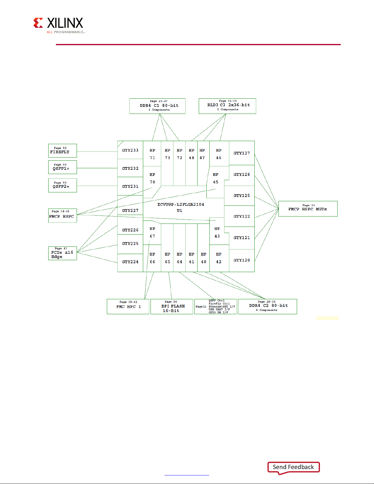
Board Component Location
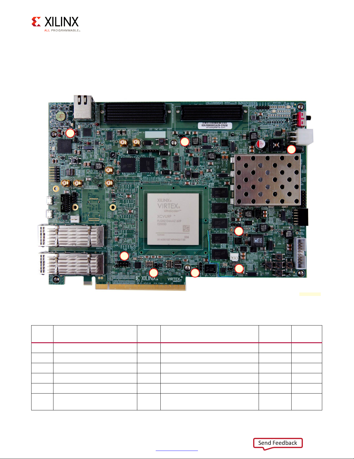
Figure 2-1 shows the VCU118 board component locations. Each numbered component
shown in the figure is keyed to Table 2-1. Table 2-1 identifies the components, references
the respective schematic page numbers, and links to a detailed functional description of the
components and board features in Chapter 3.
IMPORTANT: Figure 2-1 is for visual reference only and might not reflect the current revision of the
board.
CAUTION! The VCU118 board can be damaged by electrostatic discharge (ESD). Follow standard ESD
prevention measures when handling the board.
Chapter 2
VCU118 Board User Guide 10
UG1224 (v1.0) December 15, 2016
www.xilinx.com
Page 11

X-Ref Target - Figure 2-1
Round callout references a component
on the front side of the board
Square callout references a component
on the backside side of the board
9
7
20
19
36
28
38
8
21
14
18
26
17
4
C1
40
5
33
34
22
15
27
23
24
30
39
29
37
25
11
31
31
4
C2
16
13 12 35
6 10
11
2
1
3
00
00
41
X18022-102616
Send Feedback
Chapter 2: Board Setup and Configuration
Table 2-1: VCU118 Board Component Descriptions
Callout Feature Notes
VCU118 Board User Guide 11
UG1224 (v1.0) December 15, 2016
Virtex UltraScale+ XCVU9P-L2FLGA2104
1
Device, (with fan-sink on soldered FPGA)
GTY transceivers, Right Side Quads (six
2
quads)
GTY transceivers, Left Side Quads (seven
3
quads)
DDR4 Component Memory, two 80-bit DDR4
4
component memory I/F, C1 (U60-U64)
Figure 2-1: VCU118 Evaluation Board Components
(bottom) and C2 (U135-U139) (top)
RLD3 Component Memory, RLD3 72-bit
5
component memory I/F C3 (U141-U142)
www.xilinx.com
XCVU9P-L2FLGA2104E
Cofan 30-5530-03
Embedded within FPGA U1 14-15
Embedded within FPGA U1 16-17
C1: 5 x Micron MT40A256M16GE-075E,
C2: 5 x Micron MT40A256M16GE-075E
Micron MT44K32M36RB-083F 31-32
Schematic
Page Number
25-27,
28-30
Page 12
Table 2-1: VCU118 Board Component Descriptions (Cont’d)
Send Feedback
Chapter 2: Board Setup and Configuration
Callout Feature Notes
Linear BPI Flash Memory, BPI 16-bit
6
7
8
9
10
11
12
configuration memory 1 Gb (U133)
Micro-SD Card Interface, (bottom)
Micro-SD card interface connector (J83)
Digilent USB JTAG Module, USB JTAG micro-B
connector (J106)
Digilent USB JTAG Module (U115), with
micro-B connector
Clock Generation, multi-output clock
generator, SYSCLK and other clocks, 1.8V
LVDS (U122)
System Clock, programmable user clock
Si570_0, I
LVDS (U18) (bottom) with 1-to-2 LVDS
MUX/buffer (U157) (top)
Programmable User Clock 1, programmable
user clock Si570_1, I
clock, 3.3V LVDS (U32) with 1-to-2 LVDS
MUX/buffer (U104)
2
C programmable user clock, 3.3V
2
C programmable user
Micron MT28GU01GAAA1EGC-0SIT 54
Molex 5025700893 49
Hirose ZX62D-AB-5P8 24
Digilent JTAG-SMT2-NC 24
SI5335A-B02436-GM, 4 outputs:
300 MHz, 125 MHz, 90 MHz, 33.33 MHz
Silicon Labs SI570BAB0000544DG
(default 156.250 MHz) with Si53340
MUX/buffer
Silicon Labs SI570BAB0000544DG
(default 156.250 MHz) with Si53340
MUX/buffer
Schematic
Page Number
44
44
45
Programmable User Clock 2 (QSFP Clock),
13
14
15 User SMA Clock pair J34(P)/J35(N) Rosenberger 32K10K-400L5 45
16
17
18
19
20
21
22
23
programmable user clock Si570_2, I
programmable user clock, 3.3V LVDS (U38)
250 MHz Clock, fixed SG5032 250 MHz user
clock, 3.3V LVDS (U14) (bottom) with 1-to-2
LVDS MUX/buffer (U21) (bottom)
Jitter Attenuated Clock, jitter attenuated
QSFP clock (U57)
PCI Express Endpoint Connectivity, PCI
Express connector (P1)
Two 28 Gb/s QSFP+ Module Connectors,
QSFP1 (U145), QSFP2 (U123)
10/100/1000 Mb/s Tri-Speed Ethernet PHY
with RJ45, SGMII mode only, (U7, J10)
Ethernet PHY Status LEDs, LEDs are
integrated into J10 bezel
Dual USB-to-UART Bridge, bridge device
(U34) with mini-B connector (J4)
I2C Bus, Topology, and Switches, I
2
C bus MUX (U28) (bottom)
I
I2C Bus, Topology, and Switches, I
2
C bus MUX (U80)
I
2
C
2
C bus,
2
C bus,
Silicon Labs SI570BAB0000544DG
(default 156.250 MHz)
Epson SG5032VAN_250.000000M-KEGA3
with ICS85411AMLF 1-to-2 buffer
Silicon Labs SI5328B 51
8-lane card edge connector 43
Amphenol FS1-Z38-20Z6-10 50
TI DP83867ISRGZ with Wurth
7499111221A RJ45 (with magnetics)
Wurth 7499111221A RJ45 integrated
status LEDs
Silicon Labs CP2105-F01-GM bridge,
Hirose ZX62D-AB-5P8 connector
TI TCA9548APWR 58
TI TCA9548APWR 58
45
45
52
52
53
VCU118 Board User Guide 12
UG1224 (v1.0) December 15, 2016
www.xilinx.com
Page 13
Table 2-1: VCU118 Board Component Descriptions (Cont’d)
Send Feedback
Chapter 2: Board Setup and Configuration
Callout Feature Notes
24
25
26
27
28
29
30 Switches, power on/off slide switch SW1 C&K 1201M2S3AQE2 59
31
32
User GPIO LEDs (DS6-DS10, DS12, DS13,
DS18)
User Pushbuttons, (SW10, SW17, SW9, SW6,
SW7), CPU reset pushbutton (SW5) all
active-High
GPIO DIP Switch, GPIO DIP switch (SW12)
(bottom)
Program_B Pushbutton Switch, program_B
pushbutton switch, FPGA PROG pushbutton
(SW4)
VCU118 XC7Z010 system controller, mode
switch DIP, switch (SW15)
User Pmod GPIO Headers, (J52 right-angle
receptacle, J53 male pin header) (top) with
level shifters (U41,U42) (bottom)
VCU118 Board Power System, power
management system (top and bottom)
Monitoring Voltage and Current, power
management voltage and current sensing
GPIO LEDs, green 0603 Lumex
SML-LX0603GW-TR
E-Switch TL3301EF100QG (north, south,
east, west, center pattern)
4-pole CTS 218-4LPSTRF 55
E-Switch TL3301EF100QG 55
4-pole CTS 218-4LPSTRF 49
J52 Sullins PPPC062LJBN-RC,
J53 Sullins PBC36DAAN,
NXP NVT2008PW
Maxim MAX20751E and MAX15301
dig-ital P.O.L. controllers
TI Current and Power Monitor
INA226AIDGS
Page Number
Schematic
55
55
57
60-75
60-67
33 GTY Transceivers, FMCP HSPC connector J22 Samtec ASP_184329_01 34-38
34 FMC HPC1 Connector J2 Samtec ASP_134486_01 39-42
35
36
37
38
39
41 FireFly Connector, signal and power pair (J6)
40
Notes:
1. The VCU118 board schematics are available for download. See the VCU118 Evaluation Kit.
2. The VCU118 board jumper header locations are shown in Figure 2-2.
Configuration Options, FPGA U1
configuration mode DIP switch, (SW16)
System Controller, VCU118 Zynq-7000 AP
SoC XC7Z010CLG225 (U111)
Monitoring Voltage and Current, VCU118
board power system 2x8 shrouded PMBus
connector (J39)
Digilent USB JTAG Module, USB JTAG
module, shrouded JTAG cable connector (J3)
Power On/Off Slide Switch SW1, power input
connector (J15)
PCI Express Endpoint Connectivity, lane
width select header, (J7)
4-pole CTS 218-4LPSTRF 3
XC7Z010CLG225 46-49
ASSMAN AWHW16G-0202 59
2x7 2 mm Molex 87832-1420 24
2x6 Molex-39-30-1060 59
Samtec Signal: UEC5-019-2-H-D-RA-1,
Samtec Power: UCC8-10-1-H-S-1-A
2x4 0.1 inch male header Sullins
PBC36DAAN
50
43
VCU118 Board User Guide 13
UG1224 (v1.0) December 15, 2016
www.xilinx.com
Page 14
Default Switch and Jumper Settings
Send Feedback
Switches
Default switch settings are listed in Table 2-2. Switch locations are shown in Figure 2-1.
Table 2-2 also references the respective schematic page numbers.
Table 2-2: Default Switch Settings
Chapter 2: Board Setup and Configuration
Switch Function Default Comments
SW1 SPST slide switch OFF Board shipped with power switch off 30 59
SW12 4-pole GPIO 0000 Positions 1-4, GPIO 26 55
SW15 4-pole configuration 0000
SW16 4-pole configuration 0101
Notes:
1. DIP switches are active-High (connected net is pulled High when DIP switch is closed).
Positions 1-4, Zynq-7000 AP SoC System
Controller U111
Position 1, System Controller Enable
Positions 2-4, FPGA U1 mode M[2:0]
Figure 2-1
Callout
28 49
35 3
Schematic
Page
VCU118 Board User Guide 14
UG1224 (v1.0) December 15, 2016
www.xilinx.com
Page 15
X-Ref Target - Figure 2-2
8
6
5
7
3
14
2
X18026-100416
Send Feedback
Chapter 2: Board Setup and Configuration
Jumpers
Figure 2-2 shows the VCU118 board jumper header locations. Each numbered component
shown in the figure is keyed to Table 2-3, which identifies the default jumper settings and
references the respective schematic page numbers.
Table 2-3: Default Jumper Settings
Jumper Function Default Comments
J12 Maxim regulator inhibit Off Used when programming PWR. SYS. 5 59
J14 U30 VADJ_1V8 enable Off
VCU118 Board User Guide 15
UG1224 (v1.0) December 15, 2016
Figure 2-2: VCU118 Board Header Jumper Locations
J5 Power on reset (POR) override 2-3 U1 POR_OVERRIDE pin AG12 to GND 1 3
J7 PCIe lane size select 7-8 16-lane configuration 2 43
J8 SYSCLK source select Off SI5335A 300 MHz default 3 44
J9 USER/MGT_SI570 source select Off SI570 U32 156.250 MHz 4 45
Input to U25 AND, VADJ_1V8
enabled
Figure 2-2
Schematic
Callout
663
Page
www.xilinx.com
Page 16

Table 2-3: Default Jumper Settings (Cont’d)
X17987-100416
Send Feedback
Chapter 2: Board Setup and Configuration
Jumper Function Default Comments
J29 BPI Flash A25 source select 1-2 A25 connected to FPGA U1 pin BE17 7 54
J110
Zynq-7000 AP SoC System
Controller U111 QSPI_IO3
Off
QSPI_IO3 P/U w/20K (On = P/D to
GND)
Figure 2-2
Callout
847
Installing the VCU118 Board in a PC Chassis
Installation of the VCU118 board inside a computer chassis is required when developing or
testing PCI Express® functionality.
When the VCU118 board is used inside a computer chassis (that is, plugged in to the PCIe®
slot), power is provided from the ATX power supply 4-pin peripheral connector through the
ATX adapter cable (Figure 2-3) to J15 on the VCU118 board. The Xilinx part number for this
cable is 2600304. See [Ref 29] for ordering information.
X-Ref Target - Figure 2-3
Schematic
Page
VCU118 Board User Guide 16
UG1224 (v1.0) December 15, 2016
Figure 2-3: ATX Power Supply Adapter Cable
To install the VCU118 board in a PC chassis:
1. On the VCU118 board, remove the six screws retaining the six rubber feet with their
standoffs, and the PCIe bracket. Reinstall the PCIe bracket using two of the previously
removed screws.
2. Power down the host computer and remove the power cord from the PC.
3. Open the PC chassis following the instructions provided with the PC.
4. Select a vacant PCIe expansion slot and remove the expansion cover (at the back of the
chassis) by removing the screws on the top and bottom of the cover.
www.xilinx.com
Page 17
Chapter 2: Board Setup and Configuration
Send Feedback
5. The VCU118 board requires three adjacent PCIe slots. The VCU118 board has a large
cooling fan that exceeds the PCIe top side component height restriction and has several
spring loaded screws on the back side of the board. Ensure the slots closest to the front
and back of the board are free of obstructions.
6. Plug the VCU118 board into the center of the three open slots.
7. Install the top mounting bracket screw into the PC expansion cover retainer bracket to
secure the VCU118 board in its slot.
8. Connect the ATX power supply to the VCU118 board using the ATX power supply
adapter cable as shown in Figure 2-3.
a. Plug the 6-pin 2 x 3 Molex connector on the adapter cable into J15 on the VCU118
board.
b. Plug the 4-pin 1 x 4 peripheral power connector from the ATX power supply into the
4-pin adapter cable connector.
CAUTION! Do NOT plug a PC ATX power supply 6-pin connector into J15 on the VCU118 evaluation
board. The ATX 6-pin connector has a different pin out than J15. Connecting an ATX 6-pin connector
into J15 damages the VCU118 evaluation board and voids the board warranty.
9. Slide the VCU118 board power switch SW1 to the ON position. The PC can now be
powered on.
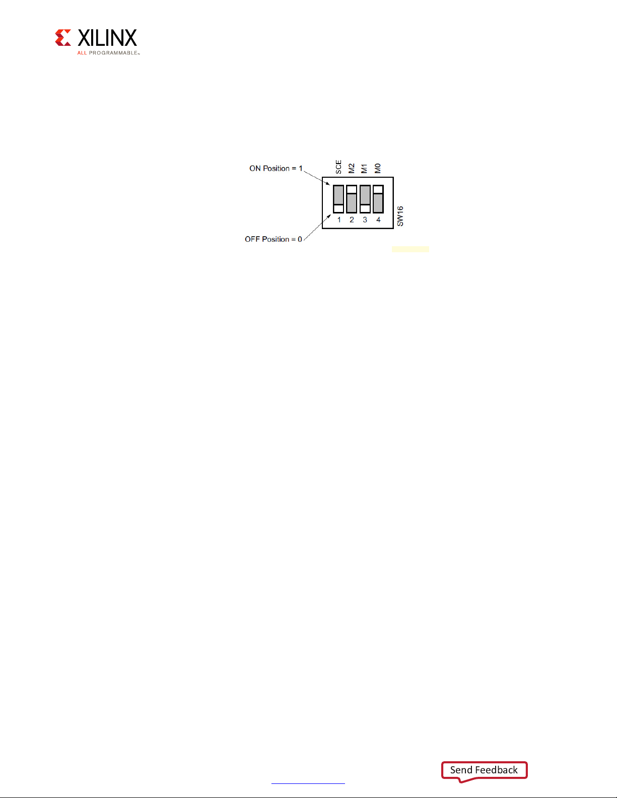
FPGA Configuration
The VCU118 board supports two of the seven UltraScale FPGA configuration modes:
• Master BPI using the onboard linear BPI flash memory
•JTAG using:
USB JTAG configuration port (Digilent module U115)
°
Platform cable USB 2.0, 2 mm, keyed flat cable header (J3)
°
Each configuration interface corresponds to one or more configuration modes and bus
widths, as listed in Table 2-4. The mode switches M2, M1, and M0 are on SW16 positions 2,
3, and 4, respectively. The FPGA default mode setting M[2:0] = 101 selects the JTAG
configuration mode.
Table 2-4: Configuration Modes
VCU118 Board User Guide 17
UG1224 (v1.0) December 15, 2016
Configuration Mode
Master BPI 010 x8,x16 Output
JTAG 101 x1 Not Applicable
SW16 DIP Switch
Settings M[2:0]
Bus Width CCLK Direction
www.xilinx.com
Page 18
Chapter 2: Board Setup and Configuration
;
Send Feedback
For complete details on configuring the FPGA, see UltraScale Architecture Configuration
User Guide (UG570) [Ref 2].
Figure 2-4 shows the configuration mode DIP switch SW16 default switch positions.
X-Ref Target - Figure 2-4
Figure 2-4: SW16 Default Settings
VCU118 Board User Guide 18
UG1224 (v1.0) December 15, 2016
www.xilinx.com
Page 19
Board Component Descriptions
Send Feedback
Overview
This chapter provides a detailed functional description of the board’s components and
features. Table 2-1, page 11 identifies the components, references the respective schematic
page numbers, and links to the corresponding detailed functional description in this
chapter. Component locations are shown in Figure 2-1, page 11.
Component Descriptions
Chapter 3
Virtex UltraScale+ XCVU9P-L2FLGA2104 Device
[Figure 2-1, callout 1]
The VCU118 board is populated with the Virtex UltraScale+ XCVU9P-L2FLGA2104 device.
For more information on Virtex UltraScale+ FPGAs, see Virtex UltraScale+ FPGAs Data
Sheet: DC and AC Switching Characteristics (DS923) [Ref 1].
VCU118 Board User Guide 19
UG1224 (v1.0) December 15, 2016
www.xilinx.com
Page 20
Chapter 3: Board Component Descriptions
To VBATT pin
U1.AT11
X18008-100416
Send Feedback
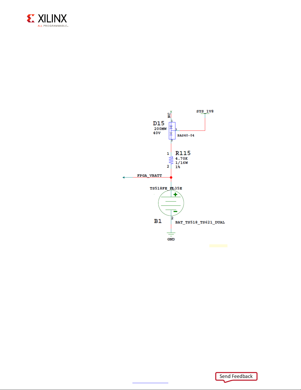
Encryption Key Battery Backup Circuit
The XCVU9P device U1 implements bitstream encryption key technology. The VCU118
board provides the encryption key backup battery circuit shown in Figure 3-1. The Seiko
TS518FE rechargeable 1.5V lithium button-type battery B1 is soldered to the board with the
positive output connected to the XCVU9P device U1 VBATT pin AT11. The battery supply
current I
from the SYS_1V8 1.8V rail through a series diode with a typical forward voltage drop of
0.38V and 4.7 KΩ current limit resistor. The nominal charging voltage is 1.42V.
X-Ref Target - Figure 3-1
specification is 150 nA maximum when the board power is off. B1 is charged
BATT
VCU118 Board User Guide 20
UG1224 (v1.0) December 15, 2016
Figure 3-1: Encryption Key Backup Circuit
www.xilinx.com
Page 21
Chapter 3: Board Component Descriptions
Send Feedback
I/O Voltage Rails
There are 16 I/O banks available on the XCVU9P device and the VCU118 board. The voltages
applied to the FPGA I/O banks used by the VCU118 board are listed in Table 3-1.
Table 3-1: I/O Bank Voltage Rails
FPGA (U1) Bank Power Supply Rail Net Name Voltage
Bank 0 VCC1V8_FPGA 1.8V
HP Bank 40 VCC1V2_FPGA 1.2V
HP Bank 41 VCC1V2_FPGA 1.2V
HP Bank 42 VCC1V2_FPGA 1.2V
HP Bank 43 VADJ_1V8_FPGA 1.8V
HP Bank 45 VADJ_1V8_FPGA 1.8V
HP Bank 46 VCC1V2_FPGA 1.2V
HP Bank 47 VCC1V2_FPGA 1.2V
HP Bank 48 VCC1V2_FPGA 1.2V
HP Bank 64 VCC1V8_FPGA 1.8V
HP Bank 65 VCC1V8_FPGA 1.8V
HP Bank 66 VADJ_1V8_FPGA 1.8V
HP Bank 67 VADJ_1V8_FPGA 1.8V
HP Bank 70 VADJ_1V8_FPGA 1.8V
HP Bank 71 VCC1V2_FPGA 1.2V
HP Bank 72 VCC1V2_FPGA 1.2V
HR Bank 73 VCC1V2_FPGA 1.2V
VCU118 Board User Guide 21
UG1224 (v1.0) December 15, 2016
www.xilinx.com
Page 22

Chapter 3: Board Component Descriptions
Send Feedback
DDR4 Component Memory
[Figure 2-1, callout 4]
The 2.5 GB DDR4 component memory system is comprised of two sets of five 256 Mb x 16
(80-bit wide) DDR4 SDRAM devices (Micron MT40A256M16GE-075E) located at U60-U64
(C1) and U135-U139 (C2). This dual memory system is connected in 80-bit wide interfaces
to the U1 XCVU9P HP banks 71, 72, 73 (C1) and 40, 41, 42 (C2). The DDR4 0.6V VTT
termination voltages (nets DDR4_C1_VTT and DDR4_C2_VTT) are sourced from the TI
TPS51200DR linear regulators U24 and U134. The DDR4 memory interface bank VREF pins
are not connected, which, coupled with an XDC set_property INTERNAL_VREF constraint,
invoke the INTERNAL VREF mode. The connections between the C1 80-bit interface DDR4
component memories and XCVU9P banks 71, 72, and 73 are listed in Table 3-2.
Table 3-2: DDR4 Memory 80-bit I/F C1 to FPGA U1 Banks 71, 72, and 73
FPGA (U1)
Pin
F11 DDR4_C1_DQ0 POD12_DCI G2 DQL0 U60
E11 DDR4_C1_DQ1 POD12_DCI F7 DQL1 U60
F10 DDR4_C1_DQ2 POD12_DCI H3 DQL2 U60
F9 DDR4_C1_DQ3 POD12_DCI H7 DQL3 U60
H12 DDR4_C1_DQ4 POD12_DCI H2 DQL4 U60
G12 DDR4_C1_DQ5 POD12_DCI H8 DQL5 U60
E9 DDR4_C1_DQ6 POD12_DCI J3 DQL6 U60
D9 DDR4_C1_DQ7 POD12_DCI J7 DQL7 U60
R19 DDR4_C1_DQ8 POD12_DCI A3 DQU0 U60
P19 DDR4_C1_DQ9 POD12_DCI B8 DQU1 U60
M18 DDR4_C1_DQ10 POD12_DCI C3 DQU2 U60
M17 DDR4_C1_DQ11 POD12_DCI C7 DQU3 U60
N19 DDR4_C1_DQ12 POD12_DCI C2 DQU4 U60
N18 DDR4_C1_DQ13 POD12_DCI C8 DQU5 U60
N17 DDR4_C1_DQ14 POD12_DCI D3 DQU6 U60
Schematic Net Name I/O Standard
Pin # Pin Name Ref. Des.
Component Memory
VCU118 Board User Guide 22
UG1224 (v1.0) December 15, 2016
M16 DDR4_C1_DQ15 POD12_DCI D7 DQU7 U60
D11 DDR4_C1_DQS0_T DIFF_POD12_DCI G3 DQSL_T U60
D10 DDR4_C1_DQS0_C DIFF_POD12_DCI F3 DQSL_C U60
P17 DDR4_C1_DQS1_T DIFF_POD12_DCI B7 DQSU_T U60
P16 DDR4_C1_DQS1_C DIFF_POD12_DCI A7 DQSU_C U60
G11 DDR4_C1_DM0 POD12_DCI E7 DML_B/DBIL_B U60
R18 DDR4_C1_DM1 POD12_DCI E2 DMU_B/DBIU_B U60
L16 DDR4_C1_DQ16 POD12_DCI G2 DQL0 U61
www.xilinx.com
Page 23
Chapter 3: Board Component Descriptions
Send Feedback
Table 3-2: DDR4 Memory 80-bit I/F C1 to FPGA U1 Banks 71, 72, and 73 (Cont’d)
FPGA (U1)
Pin
K16 DDR4_C1_DQ17 POD12_DCI F7 DQL1 U61
L18 DDR4_C1_DQ18 POD12_DCI H3 DQL2 U61
K18 DDR4_C1_DQ19 POD12_DCI H7 DQL3 U61
J17 DDR4_C1_DQ20 POD12_DCI H2 DQL4 U61
H17 DDR4_C1_DQ21 POD12_DCI H8 DQL5 U61
H19 DDR4_C1_DQ22 POD12_DCI J3 DQL6 U61
H18 DDR4_C1_DQ23 POD12_DCI J7 DQL7 U61
F19 DDR4_C1_DQ24 POD12_DCI A3 DQU0 U61
F18 DDR4_C1_DQ25 POD12_DCI B8 DQU1 U61
E19 DDR4_C1_DQ26 POD12_DCI C3 DQU2 U61
E18 DDR4_C1_DQ27 POD12_DCI C7 DQU3 U61
G20 DDR4_C1_DQ28 POD12_DCI C2 DQU4 U61
F20 DDR4_C1_DQ29 POD12_DCI C8 DQU5 U61
E17 DDR4_C1_DQ30 POD12_DCI D3 DQU6 U61
D16 DDR4_C1_DQ31 POD12_DCI D7 DQU7 U61
Schematic Net Name I/O Standard
Pin # Pin Name Ref. Des.
Component Memory
K19 DDR4_C1_DQS2_T DIFF_POD12_DCI G3 DQSL_T U61
J19 DDR4_C1_DQS2_C DIFF_POD12_DCI F3 DQSL_C U61
F16 DDR4_C1_DQS3_T DIFF_POD12_DCI B7 DQSU_T U61
E16 DDR4_C1_DQS3_C DIFF_POD12_DCI A7 DQSU_C U61
K17 DDR4_C1_DM2 POD12_DCI E7 DML_B/DBIL_B U61
G18 DDR4_C1_DM3 POD12_DCI E2 DMU_B/DBIU_B U61
D17 DDR4_C1_DQ32 POD12_DCI G2 DQL0 U62
C17 DDR4_C1_DQ33 POD12_DCI F7 DQL1 U62
C19 DDR4_C1_DQ34 POD12_DCI H3 DQL2 U62
C18 DDR4_C1_DQ35 POD12_DCI H7 DQL3 U62
D20 DDR4_C1_DQ36 POD12_DCI H2 DQL4 U62
D19 DDR4_C1_DQ37 POD12_DCI H8 DQL5 U62
C20 DDR4_C1_DQ38 POD12_DCI J3 DQL6 U62
B20 DDR4_C1_DQ39 POD12_DCI J7 DQL7 U62
N23 DDR4_C1_DQ40 POD12_DCI A3 DQU0 U62
M23 DDR4_C1_DQ41 POD12_DCI B8 DQU1 U62
R21 DDR4_C1_DQ42 POD12_DCI C3 DQU2 U62
VCU118 Board User Guide 23
UG1224 (v1.0) December 15, 2016
P21 DDR4_C1_DQ43 POD12_DCI C7 DQU3 U62
R22 DDR4_C1_DQ44 POD12_DCI C2 DQU4 U62
www.xilinx.com
Page 24

Chapter 3: Board Component Descriptions
Send Feedback
Table 3-2: DDR4 Memory 80-bit I/F C1 to FPGA U1 Banks 71, 72, and 73 (Cont’d)
FPGA (U1)
Pin
P22 DDR4_C1_DQ45 POD12_DCI C8 DQU5 U62
T23 DDR4_C1_DQ46 POD12_DCI D3 DQU6 U62
R23 DDR4_C1_DQ47 POD12_DCI D7 DQU7 U62
A19 DDR4_C1_DQS4_T DIFF_POD12_DCI G3 DQSL_T U62
A18 DDR4_C1_DQS4_C DIFF_POD12_DCI F3 DQSL_C U62
N22 DDR4_C1_DQS5_T DIFF_POD12_DCI B7 DQSU_T U62
M22 DDR4_C1_DQS5_C DIFF_POD12_DCI A7 DQSU_C U62
B18 DDR4_C1_DM4 POD12_DCI E7 DML_B/DBIL_B U62
P20 DDR4_C1_DM5 POD12_DCI E2 DMU_B/DBIU_B U62
K24 DDR4_C1_DQ48 POD12_DCI G2 DQL0 U63
J24 DDR4_C1_DQ49 POD12_DCI F7 DQL1 U63
M21 DDR4_C1_DQ50 POD12_DCI H3 DQL2 U63
L21 DDR4_C1_DQ51 POD12_DCI H7 DQL3 U63
K21 DDR4_C1_DQ52 POD12_DCI H2 DQL4 U63
J21 DDR4_C1_DQ53 POD12_DCI H8 DQL5 U63
Schematic Net Name I/O Standard
Pin # Pin Name Ref. Des.
Component Memory
K22 DDR4_C1_DQ54 POD12_DCI J3 DQL6 U63
J22 DDR4_C1_DQ55 POD12_DCI J7 DQL7 U63
H23 DDR4_C1_DQ56 POD12_DCI A3 DQU0 U63
H22 DDR4_C1_DQ57 POD12_DCI B8 DQU1 U63
E23 DDR4_C1_DQ58 POD12_DCI C3 DQU2 U63
E22 DDR4_C1_DQ59 POD12_DCI C7 DQU3 U63
F21 DDR4_C1_DQ60 POD12_DCI C2 DQU4 U63
E21 DDR4_C1_DQ61 POD12_DCI C8 DQU5 U63
F24 DDR4_C1_DQ62 POD12_DCI D3 DQU6 U63
F23 DDR4_C1_DQ63 POD12_DCI D7 DQU7 U63
M20 DDR4_C1_DQS6_T DIFF_POD12_DCI G3 DQSL_T U63
L20 DDR4_C1_DQS6_C DIFF_POD12_DCI F3 DQSL_C U63
H24 DDR4_C1_DQS7_T DIFF_POD12_DCI B7 DQSU_T U63
G23 DDR4_C1_DQS7_C DIFF_POD12_DCI A7 DQSU_C U63
L23 DDR4_C1_DM6 POD12_DCI E7 DML_B/DBIL_B U63
G22 DDR4_C1_DM7 POD12_DCI E2 DMU_B/DBIU_B U63
A24 DDR4_C1_DQ64 POD12_DCI G2 DQL0 U64
VCU118 Board User Guide 24
UG1224 (v1.0) December 15, 2016
A23 DDR4_C1_DQ65 POD12_DCI F7 DQL1 U64
C24 DDR4_C1_DQ66 POD12_DCI H3 DQL2 U64
www.xilinx.com
Page 25

Chapter 3: Board Component Descriptions
Send Feedback
Table 3-2: DDR4 Memory 80-bit I/F C1 to FPGA U1 Banks 71, 72, and 73 (Cont’d)
FPGA (U1)
Pin
C23 DDR4_C1_DQ67 POD12_DCI H7 DQL3 U64
B23 DDR4_C1_DQ68 POD12_DCI H2 DQL4 U64
B22 DDR4_C1_DQ69 POD12_DCI H8 DQL5 U64
B21 DDR4_C1_DQ70 POD12_DCI J3 DQL6 U64
A21 DDR4_C1_DQ71 POD12_DCI J7 DQL7 U64
D7 DDR4_C1_DQ72 POD12_DCI A3 DQU0 U64
C7 DDR4_C1_DQ73 POD12_DCI B8 DQU1 U64
B8 DDR4_C1_DQ74 POD12_DCI C3 DQU2 U64
B7 DDR4_C1_DQ75 POD12_DCI C7 DQU3 U64
C10 DDR4_C1_DQ76 POD12_DCI C2 DQU4 U64
B10 DDR4_C1_DQ77 POD12_DCI C8 DQU5 U64
B11 DDR4_C1_DQ78 POD12_DCI D3 DQU6 U64
A11 DDR4_C1_DQ79 POD12_DCI D7 DQU7 U64
D22 DDR4_C1_DQS8_T DIFF_POD12_DCI G3 DQSL_T U64
C22 DDR4_C1_DQS8_C DIFF_POD12_DCI F3 DQSL_C U64
Schematic Net Name I/O Standard
Pin # Pin Name Ref. Des.
Component Memory
A9 DDR4_C1_DQS9_T DIFF_POD12_DCI B7 DQSU_T U64
A8 DDR4_C1_DQS9_C DIFF_POD12_DCI A7 DQSU_C U64
E24 DDR4_C1_DM8 POD12_DCI E7 DML_B/DBIL_B U64
C9 DDR4_C1_DM9 POD12_DCI E2 DMU_B/DBIU_B U64
D14 DDR4_C1_A0 SSTL12_DCI P3 A0 U60-U64
B15 DDR4_C1_A1 SSTL12_DCI P7 A1 U60-U64
B16 DDR4_C1_A2 SSTL12_DCI R3 A2 U60-U64
C14 DDR4_C1_A3 SSTL12_DCI N7 A3 U60-U64
C15 DDR4_C1_A4 SSTL12_DCI N3 A4 U60-U64
A13 DDR4_C1_A5 SSTL12_DCI P8 A5 U60-U64
A14 DDR4_C1_A6 SSTL12_DCI P2 A6 U60-U64
A15 DDR4_C1_A7 SSTL12_DCI R8 A7 U60-U64
A16 DDR4_C1_A8 SSTL12_DCI R2 A8 U60-U64
B12 DDR4_C1_A9 SSTL12_DCI R7 A9 U60-U64
C12 DDR4_C1_A10 SSTL12_DCI M3 A10/AP U60-U64
B13 DDR4_C1_A11 SSTL12_DCI T2 A11 U60-U64
C13 DDR4_C1_A12 SSTL12_DCI M7 A12/BC_B U60-U64
VCU118 Board User Guide 25
UG1224 (v1.0) December 15, 2016
D15 DDR4_C1_A13 SSTL12_DCI T8 A13 U60-U64
G15 DDR4_C1_BA0 SSTL12_DCI N2 BA0 U60-U64
www.xilinx.com
Page 26
Chapter 3: Board Component Descriptions
Send Feedback
Table 3-2: DDR4 Memory 80-bit I/F C1 to FPGA U1 Banks 71, 72, and 73 (Cont’d)
FPGA (U1)
Pin
G13 DDR4_C1_BA1 SSTL12_DCI N8 BA1 U60-U64
H13 DDR4_C1_BG0 SSTL12_DCI M2 BG0 U60-U64
H14 DDR4_C1_A14_WE_B SSTL12_DCI L2 WE_B/A14 U60-U64
H15 DDR4_C1_A15_CAS_B SSTL12_DCI M8 CAS_B_A15 U60-U64
F15 DDR4_C1_A16_RAS_B SSTL12_DCI L8 RAS_B/A16 U60-U64
F14 DDR4_C1_CK_T DIFF_SSTL12_DCI K7 CK_T U60-U64
E14 DDR4_C1_CK_C DIFF_SSTL12_DCI K8 CK_C U60-U64
A10 DDR4_C1_CKE SSTL12_DCI K2 CKE U60-U64
E13 DDR4_C1_ACT_B SSTL12_DCI L3 ACT_B U60-U64
G10 DDR4_C1_PAR SSTL12_DCI T3 PAR U60-U64
C8 DDR4_C1_ODT SSTL12_DCI K3 ODT U60-U64
F13 DDR4_C1_CS_B SSTL12_DCI L7 CS_B U60-U64
R17 DDR4_C1_ALERT_B SSTL12_DCI P9 ALERT_B U60-U64
N20 DDR4_C1_RESET_B LVCMOS12 P1 RESET_B U60-U64
A20 DDR4_C1_TEN SSTL12_DCI N9 TEN U60-U64
Schematic Net Name I/O Standard
Pin # Pin Name Ref. Des.
Component Memory
The connections between the C2 80-bit interface DDR4 component memories (U135-U139)
and XCVU9P banks 40, 41, and 42 are listed in Table 3-3.
Table 3-3: DDR4 Memory 80-bit I/F C2 to FPGA U1 Banks 40, 41, and 42
FPGA (U1)
Pin
BD30 DDR4_C2_DQ0 POD12_DCI G2 DQL0 U135
BE30 DDR4_C2_DQ1 POD12_DCI F7 DQL1 U135
BD32 DDR4_C2_DQ2 POD12_DCI H3 DQL2 U135
BE33 DDR4_C2_DQ3 POD12_DCI H7 DQL3 U135
BC33 DDR4_C2_DQ4 POD12_DCI H2 DQL4 U135
BD33 DDR4_C2_DQ5 POD12_DCI H8 DQL5 U135
BC31 DDR4_C2_DQ6 POD12_DCI J3 DQL6 U135
BD31 DDR4_C2_DQ7 POD12_DCI J7 DQL7 U135
BA32 DDR4_C2_DQ8 POD12_DCI A3 DQU0 U135
BB33 DDR4_C2_DQ9 POD12_DCI B8 DQU1 U135
BA30 DDR4_C2_DQ10 POD12_DCI C3 DQU2 U135
BA31 DDR4_C2_DQ11 POD12_DCI C7 DQU3 U135
Schematic Net Name I/O Standard
Pin # Pin Name Ref. Des.
Component Memory
VCU118 Board User Guide 26
UG1224 (v1.0) December 15, 2016
www.xilinx.com
Page 27
Chapter 3: Board Component Descriptions
Send Feedback
Table 3-3: DDR4 Memory 80-bit I/F C2 to FPGA U1 Banks 40, 41, and 42 (Cont’d)
FPGA (U1)
Pin
AW31 DDR4_C2_DQ12 POD12_DCI C2 DQU4 U135
AW32 DDR4_C2_DQ13 POD12_DCI C8 DQU5 U135
AY32 DDR4_C2_DQ14 POD12_DCI D3 DQU6 U135
AY33 DDR4_C2_DQ15 POD12_DCI D7 DQU7 U135
BF30 DDR4_C2_DQS0_T DIFF_POD12_DCI G3 DQSL_T U135
BF31 DDR4_C2_DQS0_C DIFF_POD12_DCI F3 DQSL_C U135
AY34 DDR4_C2_DQS1_T DIFF_POD12_DCI B7 DQSU_T U135
BA34 DDR4_C2_DQS1_C DIFF_POD12_DCI A7 DQSU_C U135
BE32 DDR4_C2_DM0 POD12_DCI E7 DML_B/DBIL_B U135
BB31 DDR4_C2_DM1 POD12_DCI E2 DMU_B/DBIU_B U135
AV30 DDR4_C2_DQ16 POD12_DCI G2 DQL0 U136
AW30 DDR4_C2_DQ17 POD12_DCI F7 DQL1 U136
AU33 DDR4_C2_DQ18 POD12_DCI H3 DQL2 U136
AU34 DDR4_C2_DQ19 POD12_DCI H7 DQL3 U136
AT31 DDR4_C2_DQ20 POD12_DCI H2 DQL4 U136
Schematic Net Name I/O Standard
Pin # Pin Name Ref. Des.
Component Memory
AU32 DDR4_C2_DQ21 POD12_DCI H8 DQL5 U136
AU31 DDR4_C2_DQ22 POD12_DCI J3 DQL6 U136
AV31 DDR4_C2_DQ23 POD12_DCI J7 DQL7 U136
AR33 DDR4_C2_DQ24 POD12_DCI A3 DQU0 U136
AT34 DDR4_C2_DQ25 POD12_DCI B8 DQU1 U136
AT29 DDR4_C2_DQ26 POD12_DCI C3 DQU2 U136
AT30 DDR4_C2_DQ27 POD12_DCI C7 DQU3 U136
AP30 DDR4_C2_DQ28 POD12_DCI C2 DQU4 U136
AR30 DDR4_C2_DQ29 POD12_DCI C8 DQU5 U136
AN30 DDR4_C2_DQ30 POD12_DCI D3 DQU6 U136
AN31 DDR4_C2_DQ31 POD12_DCI D7 DQU7 U136
AU29 DDR4_C2_DQS2_T DIFF_POD12_DCI G3 DQSL_C U136
AV29 DDR4_C2_DQS2_C DIFF_POD12_DCI F3 DQSL_T U136
AP31 DDR4_C2_DQS3_T DIFF_POD12_DCI B7 DQSU_C U136
AP32 DDR4_C2_DQS3_C DIFF_POD12_DCI A7 DQSU_T U136
AV33 DDR4_C2_DM2 POD12_DCI E7 DML_B/DBIL_B U136
AR32 DDR4_C2_DM3 POD12_DCI E2 DMU_B/DBIU_B U136
VCU118 Board User Guide 27
UG1224 (v1.0) December 15, 2016
BE34 DDR4_C2_DQ32 POD12_DCI G2 DQL0 U137
BF34 DDR4_C2_DQ33 POD12_DCI F7 DQL1 U137
www.xilinx.com
Page 28

Chapter 3: Board Component Descriptions
Send Feedback
Table 3-3: DDR4 Memory 80-bit I/F C2 to FPGA U1 Banks 40, 41, and 42 (Cont’d)
FPGA (U1)
Pin
BC35 DDR4_C2_DQ34 POD12_DCI H3 DQL2 U137
BC36 DDR4_C2_DQ35 POD12_DCI H7 DQL3 U137
BD36 DDR4_C2_DQ36 POD12_DCI H2 DQL4 U137
BE37 DDR4_C2_DQ37 POD12_DCI H8 DQL5 U137
BF36 DDR4_C2_DQ38 POD12_DCI J3 DQL6 U137
BF37 DDR4_C2_DQ39 POD12_DCI J7 DQL7 U137
BD37 DDR4_C2_DQ40 POD12_DCI A3 DQU0 U137
BE38 DDR4_C2_DQ41 POD12_DCI B8 DQU1 U137
BC39 DDR4_C2_DQ42 POD12_DCI C3 DQU2 U137
BD40 DDR4_C2_DQ43 POD12_DCI C7 DQU3 U137
BB38 DDR4_C2_DQ44 POD12_DCI C2 DQU4 U137
BB39 DDR4_C2_DQ45 POD12_DCI C8 DQU5 U137
BC38 DDR4_C2_DQ46 POD12_DCI D3 DQU6 U137
BD38 DDR4_C2_DQ47 POD12_DCI D7 DQU7 U137
BE35 DDR4_C2_DQS4_T DIFF_POD12_DCI G3 DQSL_T U137
Schematic Net Name I/O Standard
Pin # Pin Name Ref. Des.
Component Memory
BF35 DDR4_C2_DQS4_C DIFF_POD12_DCI F3 DQSL_C U137
BE39 DDR4_C2_DQS5_T DIFF_POD12_DCI B7 DQSU_T U137
BF39 DDR4_C2_DQS5_C DIFF_POD12_DCI A7 DQSU_C U137
BC34 DDR4_C2_DM4 POD12_DCI E7 DML_B/DBIL_B U137
BE40 DDR4_C2_DM5 POD12_DCI E2 DMU_B/DBIU_B U137
BB36 DDR4_C2_DQ48 POD12_DCI G2 DQL0 U138
BB37 DDR4_C2_DQ49 POD12_DCI F7 DQL1 U138
BA39 DDR4_C2_DQ50 POD12_DCI H3 DQL2 U138
BA40 DDR4_C2_DQ51 POD12_DCI H7 DQL3 U138
AW40 DDR4_C2_DQ52 POD12_DCI H2 DQL4 U138
AY40 DDR4_C2_DQ53 POD12_DCI H8 DQL5 U138
AY38 DDR4_C2_DQ54 POD12_DCI J3 DQL6 U138
AY39 DDR4_C2_DQ55 POD12_DCI J7 DQL7 U138
AW35 DDR4_C2_DQ56 POD12_DCI A3 DQU0 U138
AW36 DDR4_C2_DQ57 POD12_DCI B8 DQU1 U138
AU40 DDR4_C2_DQ58 POD12_DCI C3 DQU2 U138
AV40 DDR4_C2_DQ59 POD12_DCI C7 DQU3 U138
VCU118 Board User Guide 28
UG1224 (v1.0) December 15, 2016
AU38 DDR4_C2_DQ60 POD12_DCI C2 DQU4 U138
AU39 DDR4_C2_DQ61 POD12_DCI C8 DQU5 U138
www.xilinx.com
Page 29

Chapter 3: Board Component Descriptions
Send Feedback
Table 3-3: DDR4 Memory 80-bit I/F C2 to FPGA U1 Banks 40, 41, and 42 (Cont’d)
FPGA (U1)
Pin
AV38 DDR4_C2_DQ62 POD12_DCI D3 DQU6 U138
AV39 DDR4_C2_DQ63 POD12_DCI D7 DQU7 U138
BA35 DDR4_C2_DQS6_T DIFF_POD12_DCI G3 DQSL_C U138
BA36 DDR4_C2_DQS6_C DIFF_POD12_DCI F3 DQSL_T U138
AW37 DDR4_C2_DQS7_T DIFF_POD12_DCI B7 DQSU_C U138
AW38 DDR4_C2_DQS7_C DIFF_POD12_DCI A7 DQSU_T U138
AY37 DDR4_C2_DM6 POD12_DCI E7 DML_B/DBIL_B U138
AV35 DDR4_C2_DM7 POD12_DCI E2 DMU_B/DBIU_B U138
BF26 DDR4_C2_DQ64 POD12_DCI G2 DQL0 U139
BF27 DDR4_C2_DQ65 POD12_DCI F7 DQL1 U139
BD28 DDR4_C2_DQ66 POD12_DCI H3 DQL2 U139
BE28 DDR4_C2_DQ67 POD12_DCI H7 DQL3 U139
BD27 DDR4_C2_DQ68 POD12_DCI H2 DQL4 U139
BE27 DDR4_C2_DQ69 POD12_DCI H8 DQL5 U139
BD25 DDR4_C2_DQ70 POD12_DCI J3 DQL6 U139
Schematic Net Name I/O Standard
Pin # Pin Name Ref. Des.
Component Memory
BD26 DDR4_C2_DQ71 POD12_DCI J7 DQL7 U139
BC25 DDR4_C2_DQ72 POD12_DCI A3 DQU0 U139
BC26 DDR4_C2_DQ73 POD12_DCI B8 DQU1 U139
BB28 DDR4_C2_DQ74 POD12_DCI C3 DQU2 U139
BC28 DDR4_C2_DQ75 POD12_DCI C7 DQU3 U139
AY27 DDR4_C2_DQ76 POD12_DCI C2 DQU4 U139
AY28 DDR4_C2_DQ77 POD12_DCI C8 DQU5 U139
BA27 DDR4_C2_DQ78 POD12_DCI D3 DQU6 U139
BB27 DDR4_C2_DQ79 POD12_DCI D7 DQU7 U139
BE25 DDR4_C2_DQS8_T DIFF_POD12_DCI G3 DQSL_C U139
BF25 DDR4_C2_DQS8_C DIFF_POD12_DCI F3 DQSL_T U139
BA26 DDR4_C2_DQS9_T DIFF_POD12_DCI B7 DQSU_C U139
BB26 DDR4_C2_DQS9_C DIFF_POD12_DCI A7 DQSU_T U139
BE29 DDR4_C2_DM8 POD12_DCI E7 DML_B/DBIL_B U139
BA29 DDR4_C2_DM9 POD12_DCI E2 DMU_B/DBIU_B U139
AM27 DDR4_C2_A0 SSTL12_DCI P3 A0 U135-U139
AL27 DDR4_C2_A1 SSTL12_DCI P7 A1 U135-U139
VCU118 Board User Guide 29
UG1224 (v1.0) December 15, 2016
AP26 DDR4_C2_A2 SSTL12_DCI R3 A2 U135-U139
AP25 DDR4_C2_A3 SSTL12_DCI N7 A3 U135-U139
www.xilinx.com
Page 30
Chapter 3: Board Component Descriptions
Send Feedback
Table 3-3: DDR4 Memory 80-bit I/F C2 to FPGA U1 Banks 40, 41, and 42 (Cont’d)
FPGA (U1)
Pin
AN28 DDR4_C2_A4 SSTL12_DCI N3 A4 U135-U139
AM28 DDR4_C2_A5 SSTL12_DCI P8 A5 U135-U139
AP28 DDR4_C2_A6 SSTL12_DCI P2 A6 U135-U139
AP27 DDR4_C2_A7 SSTL12_DCI R8 A7 U135-U139
AN26 DDR4_C2_A8 SSTL12_DCI R2 A8 U135-U139
AM26 DDR4_C2_A9 SSTL12_DCI R7 A9 U135-U139
AR28 DDR4_C2_A10 SSTL12_DCI M3 A10/AP U135-U139
AR27 DDR4_C2_A11 SSTL12_DCI T2 A11 U135-U139
AV25 DDR4_C2_A12 SSTL12_DCI M7 A12/BC_B U135-U139
AT25 DDR4_C2_A13 SSTL12_DCI T8 A13 U135-U139
AR25 DDR4_C2_BA0 SSTL12_DCI N2 BA0 U135-U139
AU28 DDR4_C2_BA1 SSTL12_DCI N8 BA1 U135-U139
AU27 DDR4_C2_BG0 SSTL12_DCI M2 BG0 U135-U139
AV28 DDR4_C2_A14_WE_B SSTL12_DCI L2 WE_B/A14 U135-U139
AU26 DDR4_C2_A15_CAS_B SSTL12_DCI M8 CAS_B_A15 U135-U139
Schematic Net Name I/O Standard
Pin # Pin Name Ref. Des.
Component Memory
AV26 DDR4_C2_A16_RAS_B SSTL12_DCI L8 RAS_B/A16 U135-U139
AT26 DDR4_C2_CK_T DIFF_SSTL12_DCI K7 CK_T U135-U139
AT27 DDR4_C2_CK_C DIFF_SSTL12_DCI K8 CK_C U135-U139
AW28 DDR4_C2_CKE SSTL12_DCI K2 CKE U135-U139
AN25 DDR4_C2_ACT_B SSTL12_DCI L3 ACT_B U135-U139
BF29 DDR4_C2_PAR SSTL12_DCI P9 ALERT_B U135-U139
BB29 DDR4_C2_ODT SSTL12_DCI T3 PAR U135-U139
AY29 DDR4_C2_CS_B SSTL12_DCI K3 ODT U135-U139
AR29 DDR4_C2_ALERT_B SSTL12_DCI L7 CS_B U135-U139
BD35 DDR4_C2_RESET_B LVCMOS12 P1 RESET_B U135-U139
AY35 DDR4_C2_TEN SSTL12_DCI N9 TEN U135-U139
The VCU118 dual DDR4 80-bit memory component interfaces adhere to the constraints
guidelines documented in the “DDR3/DDR4 Design Guidelines” section of the UltraScale
Architecture-Based FPGAs Memory IP LogiCORE IP Product Guide (PG150) [Ref 4]. The
VCU118 board DDR4 memory component interface is a 40Ω impedance implementation.
For more information on the internal VREF, see the “Supply Voltages for the SelectIO Pins
VREF” and the “Internal VREF” sections in the UltraScale Architecture SelectIO Resources User
Guide (UG571) [Ref 3]. For more details about the Micron DDR4 component memory, see
the Micron MT40A256M16GE data sheet at the Micron website [Ref 18].
VCU118 Board User Guide 30
UG1224 (v1.0) December 15, 2016
www.xilinx.com
Page 31

Chapter 3: Board Component Descriptions
Send Feedback
RLD3 Component Memory
[Figure 2-1, callout 5]
The 288 MB RLD3 72-bit wide component memory system is comprised of two 36-bit 1.125
Gb RLDRAM3 devices (Micron MT44K32M36RB-083E) located at U141-U142. This memory
system is connected to the XCVU9P HP banks 46, 47, and 48. The RLD3 0.6V VTT termination
voltage (net RLD3_C3_VTT) is sourced from TI TPS51200DR linear regulator U143. The RLD3
memory interface bank VREF pins are not connected, which, coupled with an XDC
set_property INTERNAL_VREF constraint, invoke the INTERNAL VREF mode. The
connections between the RLD3 component memories and XCVU9P banks 46, 47, and 48 are
listed in Table 3-4.
Table 3-4: RLD3 Memory 72-bit I/F to FPGA U1 Banks 46, 47, and 48
FPGA
(U1) Pin
H39 RLD3_C3_72B_DQ0 SSTL12 D11 DQ0 U141
H40 RLD3_C3_72B_DQ1 SSTL12 E10 DQ1 U141
G40 RLD3_C3_72B_DQ2 SSTL12 C8 DQ2 U141
F40 RLD3_C3_72B_DQ3 SSTL12 C10 DQ3 U141
H38 RLD3_C3_72B_DQ4 SSTL12 C12 DQ4 U141
G38 RLD3_C3_72B_DQ5 SSTL12 B9 DQ5 U141
K37 RLD3_C3_72B_DQ6 SSTL12 B11 DQ6 U141
J37 RLD3_C3_72B_DQ7 SSTL12 A8 DQ7 U141
F38 RLD3_C3_72B_DQ8 SSTL12 A10 DQ8 U141
J35 RLD3_C3_72B_DQ9 SSTL12 J10 DQ9 U141
H35 RLD3_C3_72B_DQ10 SSTL12 K11 DQ10 U141
J36 RLD3_C3_72B_DQ11 SSTL12 K13 DQ11 U141
H37 RLD3_C3_72B_DQ12 SSTL12 L8 DQ12 U141
H34 RLD3_C3_72B_DQ13 SSTL12 L10 DQ13 U141
G35 RLD3_C3_72B_DQ14 SSTL12 L12 DQ14 U141
Schematic Net Name I/O Standard
Pin # Pin Name Ref. Des.
Component Memory
F35 RLD3_C3_72B_DQ15 SSTL12 M9 DQ15 U141
F36 RLD3_C3_72B_DQ16 SSTL12 M11 DQ16 U141
G36 RLD3_C3_72B_DQ17 SSTL12 N8 DQ17 U141
E37 RLD3_C3_72B_DQ18 SSTL12 D3 DQ18 U141
E38 RLD3_C3_72B_DQ19 SSTL12 E4 DQ19 U141
C39 RLD3_C3_72B_DQ20 SSTL12 C6 DQ20 U141
B40 RLD3_C3_72B_DQ21 SSTL12 C4 DQ21 U141
A39 RLD3_C3_72B_DQ22 SSTL12 C2 DQ22 U141
VCU118 Board User Guide 31
UG1224 (v1.0) December 15, 2016
www.xilinx.com
Page 32

Chapter 3: Board Component Descriptions
Send Feedback
Table 3-4: RLD3 Memory 72-bit I/F to FPGA U1 Banks 46, 47, and 48 (Cont’d)
FPGA
(U1) Pin
A40 RLD3_C3_72B_DQ23 SSTL12 B5 DQ23 U141
D40 RLD3_C3_72B_DQ24 SSTL12 B3 DQ24 U141
C40 RLD3_C3_72B_DQ25 SSTL12 A6 DQ25 U141
B38 RLD3_C3_72B_DQ26 SSTL12 A4 DQ26 U141
D35 RLD3_C3_72B_DQ27 SSTL12 J4 DQ27 U141
C35 RLD3_C3_72B_DQ28 SSTL12 K3 DQ28 U141
D34 RLD3_C3_72B_DQ29 SSTL12 K1 DQ29 U141
C34 RLD3_C3_72B_DQ30 SSTL12 L6 DQ30 U141
B36 RLD3_C3_72B_DQ31 SSTL12 L4 DQ31 U141
B37 RLD3_C3_72B_DQ32 SSTL12 L2 DQ32 U141
B35 RLD3_C3_72B_DQ33 SSTL12 M5 DQ33 U141
A36 RLD3_C3_72B_DQ34 SSTL12 M3 DQ34 U141
A34 RLD3_C3_72B_DQ35 SSTL12 N6 DQ35 U141
F39 RLD3_C3_72B_DM0 SSTL12 B7 DM0 U141
A35 RLD3_C3_72B_DM1 SSTL12 M7 DM1 U141
Schematic Net Name I/O Standard
Pin # Pin Name Ref. Des.
Component Memory
J39 RLD3_C3_72B_QK0_P DIFF_SSTL12 D9 QK0 U141
J40 RLD3_C3_72B_QK0_N DIFF_SSTL12 E8 QK0_B U141
F34 RLD3_C3_72B_QK1_P DIFF_SSTL12 K9 QK1 U141
E34 RLD3_C3_72B_QK1_N DIFF_SSTL12 J8 QK1_B U141
E39 RLD3_C3_72B_QK2_P DIFF_SSTL12 D5 QK2 U141
D39 RLD3_C3_72B_QK2_N DIFF_SSTL12 E6 QK2_B U141
D37 RLD3_C3_72B_QK3_P DIFF_SSTL12 K5 QK3 U141
C37 RLD3_C3_72B_QK3_N DIFF_SSTL12 J6 QK3_B U141
G37 RLD3_C3_72B_QVLD0 SSTL12 J12 QVLD0 U141
A38 RLD3_C3_72B_QVLD1 SSTL12 J2 QVLD1 U141
T24 RLD3_C3_72B_DQ36 SSTL12 D11 DQ0 U142
R24 RLD3_C3_72B_DQ37 SSTL12 E10 DQ1 U142
R27 RLD3_C3_72B_DQ38 SSTL12 C8 DQ2 U142
P27 RLD3_C3_72B_DQ39 SSTL12 C10 DQ3 U142
P25 RLD3_C3_72B_DQ40 SSTL12 C12 DQ4 U142
N25 RLD3_C3_72B_DQ41 SSTL12 B9 DQ5 U142
P26 RLD3_C3_72B_DQ42 SSTL12 B11 DQ6 U142
N27 RLD3_C3_72B_DQ43 SSTL12 A8 DQ7 U142
P24 RLD3_C3_72B_DQ44 SSTL12 A10 DQ8 U142
VCU118 Board User Guide 32
UG1224 (v1.0) December 15, 2016
www.xilinx.com
Page 33

Chapter 3: Board Component Descriptions
Send Feedback
Table 3-4: RLD3 Memory 72-bit I/F to FPGA U1 Banks 46, 47, and 48 (Cont’d)
FPGA
(U1) Pin
M25 RLD3_C3_72B_DQ45 SSTL12 J10 DQ9 U142
L26 RLD3_C3_72B_DQ46 SSTL12 K11 DQ10 U142
L28 RLD3_C3_72B_DQ47 SSTL12 K13 DQ11 U142
K28 RLD3_C3_72B_DQ48 SSTL12 L8 DQ12 U142
L24 RLD3_C3_72B_DQ49 SSTL12 L10 DQ13 U142
L25 RLD3_C3_72B_DQ50 SSTL12 L12 DQ14 U142
K26 RLD3_C3_72B_DQ51 SSTL12 M9 DQ15 U142
J26 RLD3_C3_72B_DQ52 SSTL12 M11 DQ16 U142
K27 RLD3_C3_72B_DQ53 SSTL12 N8 DQ17 U142
H27 RLD3_C3_72B_DQ54 SSTL12 D3 DQ18 U142
G27 RLD3_C3_72B_DQ55 SSTL12 E4 DQ19 U142
F28 RLD3_C3_72B_DQ56 SSTL12 C6 DQ20 U142
E28 RLD3_C3_72B_DQ57 SSTL12 C4 DQ21 U142
H28 RLD3_C3_72B_DQ58 SSTL12 C2 DQ22 U142
G28 RLD3_C3_72B_DQ59 SSTL12 B5 DQ23 U142
Schematic Net Name I/O Standard
Pin # Pin Name Ref. Des.
Component Memory
E26 RLD3_C3_72B_DQ60 SSTL12 B3 DQ24 U142
E27 RLD3_C3_72B_DQ61 SSTL12 A6 DQ25 U142
G25 RLD3_C3_72B_DQ62 SSTL12 A4 DQ26 U142
B28 RLD3_C3_72B_DQ63 SSTL12 J4 DQ27 U142
A28 RLD3_C3_72B_DQ64 SSTL12 K3 DQ28 U142
C27 RLD3_C3_72B_DQ65 SSTL12 K1 DQ29 U142
B27 RLD3_C3_72B_DQ66 SSTL12 L6 DQ30 U142
B26 RLD3_C3_72B_DQ67 SSTL12 L4 DQ31 U142
A26 RLD3_C3_72B_DQ68 SSTL12 L2 DQ32 U142
D25 RLD3_C3_72B_DQ69 SSTL12 M5 DQ33 U142
D26 RLD3_C3_72B_DQ70 SSTL12 M3 DQ34 U142
C25 RLD3_C3_72B_DQ71 SSTL12 N6 DQ35 U142
N24 RLD3_C3_72B_DM2 SSTL12 B7 DM0 U142
B25 RLD3_C3_72B_DM3 SSTL12 M7 DM1 U142
T26 RLD3_C3_72B_QK4_P DIFF_SSTL12 D9 QK0 U142
R26 RLD3_C3_72B_QK4_N DIFF_SSTL12 E8 QK0_B U142
M27 RLD3_C3_72B_QK5_P DIFF_SSTL12 K9 QK1 U142
M28 RLD3_C3_72B_QK5_N DIFF_SSTL12 J8 QK1_B U142
G26 RLD3_C3_72B_QK6_P DIFF_SSTL12 D5 QK2 U142
VCU118 Board User Guide 33
UG1224 (v1.0) December 15, 2016
www.xilinx.com
Page 34

Chapter 3: Board Component Descriptions
Send Feedback
Table 3-4: RLD3 Memory 72-bit I/F to FPGA U1 Banks 46, 47, and 48 (Cont’d)
FPGA
(U1) Pin
F26 RLD3_C3_72B_QK6_N DIFF_SSTL12 E6 QK2_B U142
D27 RLD3_C3_72B_QK7_P DIFF_SSTL12 K5 QK3 U142
C28 RLD3_C3_72B_QK7_N DIFF_SSTL12 J6 QK3_B U142
J27 RLD3_C3_72B_QVLD2 DIFF_SSTL12 J12 QVLD0 U142
F25 RLD3_C3_72B_QVLD3 DIFF_SSTL12 J2 QVLD1 U142
A29 RLD3_C3_72B_A0 SSTL12 E2 A0 U141-U142
C29 RLD3_C3_72B_A1 SSTL12 F5 A1 U141-U142
D29 RLD3_C3_72B_A2 SSTL12 F4 A2 U141-U142
B30 RLD3_C3_72B_A3 SSTL12 F9 A3 U141-U142
C30 RLD3_C3_72B_A4 SSTL12 F10 A4 U141-U142
A31 RLD3_C3_72B_A5 SSTL12 F12 A5 U141-U142
A30 RLD3_C3_72B_A6 SSTL12 G3 A6 U141-U142
A33 RLD3_C3_72B_A7 SSTL12 F1 A7 U141-U142
B33 RLD3_C3_72B_A8 SSTL12 G11 A8 U141-U142
B32 RLD3_C3_72B_A9 SSTL12 F13 A9 U141-U142
Schematic Net Name I/O Standard
Pin # Pin Name Ref. Des.
Component Memory
B31 RLD3_C3_72B_A10 SSTL12 H13 A10 U141-U142
C33 RLD3_C3_72B_A11 SSTL12 D1 A11 U141-U142
C32 RLD3_C3_72B_A12 SSTL12 H11 A12 U141-U142
D30 RLD3_C3_72B_A13 SSTL12 D13 A13 U141-U142
E29 RLD3_C3_72B_A14 SSTL12 H3 A14 U141-U142
F29 RLD3_C3_72B_A15 SSTL12 G2 A15 U141-U142
D32 RLD3_C3_72B_A16 SSTL12 H4 A16 U141-U142
E32 RLD3_C3_72B_A17 SSTL12 H10 A17 U141-U142
D31 RLD3_C3_72B_A18 SSTL12 G12 A18 U141-U142
E31 RLD3_C3_72B_A19 SSTL12 H1 A19 U141-U142
R28 RLD3_C3_72B_A20 SSTL12 F2 NF_A20 U141-U142
E33 RLD3_C3_72B_BA0 SSTL12 G9 BA0 U141-U142
F33 RLD3_C3_72B_BA1 SSTL12 G5 BA1 U141-U142
F30 RLD3_C3_72B_BA2 SSTL12 H8 BA2 U141-U142
G30 RLD3_C3_72B_BA3 SSTL12 H6 BA3 U141-U142
K29 RLD3_C3_72B_WE_B SSTL12 F6 WE_B U141-U142
L30 RLD3_C3_72B_REF_B SSTL12 F8 REF_B U141-U142
H29 RLD3_C3_72B_CK_P SSTL12 H7 CK U141-U142
H30 RLD3_C3_72B_CK_N SSTL12 G7 CK_B U141-U142
VCU118 Board User Guide 34
UG1224 (v1.0) December 15, 2016
www.xilinx.com
Page 35

Chapter 3: Board Component Descriptions
Send Feedback
Table 3-4: RLD3 Memory 72-bit I/F to FPGA U1 Banks 46, 47, and 48 (Cont’d)
FPGA
(U1) Pin
L29 RLD3_C3_72B_RESET_B SSTL12 A13 RESET_B U141-U142
N29 RLD3_C3_72B_CS_B SSTL12 E12 CS_B U141-U142
K31 RLD3_C3_72B_DK0_P DIFF_SSTL12 D7 DK0 U141
J31 RLD3_C3_72B_DK0_N DIFF_SSTL12 C7 DK0_B U141
K32 RLD3_C3_72B_DK1_P DIFF_SSTL12 K7 DK1 U141
J32 RLD3_C3_72B_DK1_N DIFF_SSTL12 L7 DK1_B U141
J29 RLD3_C3_72B_DK2_P DIFF_SSTL12 D7 DK0 U142
J30 RLD3_C3_72B_DK2_N DIFF_SSTL12 C7 DK0_B U142
H33 RLD3_C3_72B_DK3_P DIFF_SSTL12 K7 DK1 U142
G33 RLD3_C3_72B_DK3_N DIFF_SSTL12 L7 DK1_B U142
Schematic Net Name I/O Standard
Pin # Pin Name Ref. Des.
Component Memory
The VCU118 RLD3 72-bit memory component interface adheres to the constraints
guidelines documented in the RLD3 Design Guidelines section of UltraScale
Architecture-Based FPGAs Memory IP LogiCORE IP Product Guide (PG150) [Ref 4]. The
VCU118 RLD3 memory component interface is a 40Ω impedance implementation. For more
information on the internal VREF, see the "Supply Voltages for the SelectIO Pins", “V
and “Internal V
” sections in UltraScale Architecture SelectIO Resources (UG571) [Ref 3].
REF
For more details about the Micron RLD3 component memory, see the Micron
MT44K32M36RB-083E Data Sheet [Ref 18].
REF
”,
VCU118 Board User Guide 35
UG1224 (v1.0) December 15, 2016
www.xilinx.com
Page 36

Chapter 3: Board Component Descriptions
Send Feedback
Linear BPI Flash Memory
[Figure 2-1, callout 6]
The linear BPI flash memory located at U133 provides 128 MB (1 Gbit) of nonvolatile
storage that can be used for configuration or software storage. The data, address, and
control signals are connected to the U1 XCVU9P bank 65. The BPI flash memory device is
packaged in a 64-pin BGA.
• Part number: MT28GU01GAAA1EGC-0SIT (Micron)
• Supply voltage: 1.8V
• Datapath width: 16 bits (with 26 address lines and 7 control signals)
• Data rate: up to 90 MHz
The linear BPI flash memory can synchronously configure the FPGA in master BPI mode at
the 90 MHz data rate supported by the MT28GU01GAAA1EGC flash memory by using a
configuration bitstream generated with BitGen options for synchronous configuration and
for a configuration clock division of one. The fastest configuration method uses the
external 90 MHz oscillator connected to the FPGA bank 65 EMCCLK pin AL20. By default,
UltraScale FPGAs use the parallel NOR flash asynchronous read in the master BPI
configuration mode.
A full XCVU9P 641,272,864-bit uncompressed bitstream requires 60% of the 1 Gbit linear
BPI NOR flash size, so one XCVU9P bitstream is supported.
The BPI flash upper address A25 pin is wired to pull-up header J29 to allow one of two
compressed bitstreams to be manually selected.
See the UltraScale Architecture Configuration User Guide (UG570) [Ref 2] for more
information.
Add these constraints for compression to designs targeted for the VCU118 board.
• When loading from BPI flash:
set_property BITSTREAM.CONFIG.EXTMASTERCCLK_EN div-1 [current_design]
set_property BITSTREAM.CONFIG.BPI_SYNC_MODE Type1 [current_design]
set_property CONFIG_MODE BPI16 [current_design]
*set_property BITSTREAM.GENERAL.COMPRESS TRUE [current_design]
Note: Compression is an optional setting that can improve indirect flash programming time.
• To match the VCU118 configuration of FPGA U1 bank 0:
set_property CFGBVS GND [current_design]
set_property CONFIG_VOLTAGE 1.8 [current_design]
VCU118 Board User Guide 36
UG1224 (v1.0) December 15, 2016
www.xilinx.com
Page 37

X-Ref Target - Figure 3-2
X18006-100416
Send Feedback
Chapter 3: Board Component Descriptions
Figure 3-2: Linear BPI 128 MB (1 Gbit) Flash Memory
VCU118 Board User Guide 37
UG1224 (v1.0) December 15, 2016
www.xilinx.com
Page 38

Chapter 3: Board Component Descriptions
Send Feedback
The connections between the BPI flash memory and the FPGA are listed in Table 3-4.
Table 3-5: BPI Flash Memory Connections to FPGA U1
FPGA (U1) Pin Net Name I/O Standard
U58 BPI Flash Memory
Pin # Pin Name
AP11 BPI_FLASH_D0 (NA BANK0) F2 DQ0
AN11 BPI_FLASH_D1 (NA BANK0) E2 DQ1
AM11 BPI_FLASH_D2 (NA BANK0) G3 DQ2
AL11 BPI_FLASH_D3 (NA BANK0) E4 DQ3
AM19 BPI_FLASH_D4 LVCMOS18 E5 DQ4
AM18 BPI_FLASH_D5 LVCMOS18 G5 DQ5
AN20 BPI_FLASH_D6 LVCMOS18 G6 DQ6
AP20 BPI_FLASH_D7 LVCMOS18 H7 DQ7
AN19 BPI_FLASH_D8 LVCMOS18 E1 DQ8
AN18 BPI_FLASH_D9 LVCMOS18 E3 DQ9
AR18 BPI_FLASH_D10 LVCMOS18 F3 DQ10
AR17 BPI_FLASH_D11 LVCMOS18 F4 DQ11
AT20 BPI_FLASH_D12 LVCMOS18 F5 DQ12
AT19 BPI_FLASH_D13 LVCMOS18 H5 DQ13
AT17 BPI_FLASH_D14 LVCMOS18 G7 DQ14
AU17 BPI_FLASH_D15 LVCMOS18 E7 DQ15
AR20 BPI_FLASH_A0 LVCMOS18 A1 A0
AR19 BPI_FLASH_A1 LVCMOS18 B1 A1
AV20 BPI_FLASH_A2 LVCMOS18 C1 A2
AW20 BPI_FLASH_A3 LVCMOS18 D1 A3
AU19 BPI_FLASH_A4 LVCMOS18 D2 A4
AU18 BPI_FLASH_A5 LVCMOS18 A2 A5
AV19 BPI_FLASH_A6 LVCMOS18 C2 A6
AV18 BPI_FLASH_A7 LVCMOS18 A3 A7
AW18 BPI_FLASH_A8 LVCMOS18 B3 A8
AY18 BPI_FLASH_A9 LVCMOS18 C3 A9
AY19 BPI_FLASH_A10 LVCMOS18 D3 A10
BA19 BPI_FLASH_A11 LVCMOS18 C4 A11
BA17 BPI_FLASH_A12 LVCMOS18 A5 A12
BB17 BPI_FLASH_A13 LVCMOS18 B5 A13
BB19 BPI_FLASH_A14 LVCMOS18 C5 A14
BC19 BPI_FLASH_A15 LVCMOS18 D7 A15
VCU118 Board User Guide 38
UG1224 (v1.0) December 15, 2016
www.xilinx.com
Page 39

Chapter 3: Board Component Descriptions
Send Feedback
Table 3-5: BPI Flash Memory Connections to FPGA U1 (Cont’d)
FPGA (U1) Pin Net Name I/O Standard
U58 BPI Flash Memory
Pin # Pin Name
BB18 BPI_FLASH_A16 LVCMOS18 D8 A16
BC18 BPI_FLASH_A17 LVCMOS18 A7 A17
AY20 BPI_FLASH_A18 LVCMOS18 B7 A18
BA20 BPI_FLASH_A19 LVCMOS18 C7 A19
BD18 BPI_FLASH_A20 LVCMOS18 C8 A20
BD17 BPI_FLASH_A21 LVCMOS18 A8 A21
BC20 BPI_FLASH_A22 LVCMOS18 G1 A22
BD20 BPI_FLASH_A23 LVCMOS18 H8 A23
BE18 BPI_FLASH_A24 LVCMOS18 B6 A24
BE17 BPI_FLASH_A25 LVCMOS18 B8 A25
NC NC NA H1 A26
BF16 BPI_FLASH_FWE_B LVCMOS18 G8 WE_B
p/u R1018 BPI_FLASH_WP_B (NA BANK0) C6 WP_B
AW17 BPI_FLASH_ADV LVCMOS18 F6 ADV_B
AC12 FPGA_INIT_B (NA BANK0) D4 RST_B
BF17 BPI_FLASH_OE_B LVCMOS18 F8 OE_B
AJ11 BPI_FLASH_CE_B (NA BANK0) B4 CE_B
AL19 BPI_WAIT LVCMOS18 F7 WAIT
AL20 FPGA_CCLK LVCMOS18 E6 CLK
Additional FPGA bitstreams can be stored and used for configuration by setting the warm
boot start address (WBSTAR) register contained in UltraScale FPGAs. More information is
available in the reconfiguration and multi-boot section in the UltraScale Architecture
Configuration User Guide (UG570) [Ref 2]. The configuration section in this document
provides details on the master BPI configuration mode. For more information about the
Micron MT28GU01GAAA1EGC-0SIT, see the Micron Technology website [Ref 18].
Micro-SD Card Interface
[Figure 2-1, callout 7]
The VCU118 board includes a secure digital input/output (SDIO) interface allowing the
U111 XC7Z010 Zynq-7000 AP SoC system controller access to general purpose nonvolatile
micro-SD memory cards and peripherals. The micro-SD card slot is designed to support
50 MHz high speed micro-SD cards.
VCU118 Board User Guide 39
UG1224 (v1.0) December 15, 2016
www.xilinx.com
Page 40

X-Ref Target - Figure 3-3
Digilent
USB
Module
(U115)
TCK
TMS
TDI
TDO
JTAG
Con
(J3)
TDO
TDI
TMS
TCK
1.8V 3.3V
U19
FPGA
TCK
TMS
TDI TDO
1.8V 3.3V
U19
Level-shifted to 3.3V
FMC
HPC1
Connector
TDITDO
FMC+
HSPC
Connector
TDITDO
1.8V 3.3V
U13
Level-shifted to 1.8V
J2 J22
SPST Bus Switch
U132
SPST Bus Switch
U26
N.C. N.C.
Level-shifted to 3.3V
To FMC HSPC J22
and FMC HPC1 J2
U1
System
Ctlr.
(U 111)
TDO
TCK
TMS
TDI
X18023-100416
Send Feedback
Chapter 3: Board Component Descriptions
Digilent USB JTAG Module
[Figure 2-1, callout 8, 9]
JTAG configuration is provided through a Digilent onboard USB-to-JTAG configuration
logic module (U115) where a host computer accesses the VCU118 board JTAG chain
through a type-A (host side) to micro-B (VCU118 board side J106) USB cable.
A 2 mm JTAG header (J3) is also provided in parallel for access by Xilinx download cables,
such as the Platform Cable USB II. JTAG initiated configuration takes priority over the
configuration method selected through the FPGA mode pins M[2:0], wired to SW16
positions [2:4]. The JTAG chain of the VCU118 board is illustrated in Figure 3-3.
For more details about the Digilent USB JTAG Module, see the Digilent website [Ref 21].
Figure 3-3: JTAG Chain Block Diagram
VCU118 Board User Guide 40
UG1224 (v1.0) December 15, 2016
www.xilinx.com
Page 41

Chapter 3: Board Component Descriptions
Send Feedback
FMC Connector JTAG Bypass
When an FMC is attached to the VCU118 board, it is automatically added to the JTAG chain
through electronically controlled single-pole single-throw (SPST) switches U26 (HSPC) and
U132 (HPC1). The SPST switches are in a normally closed state and transition to an open
state when the FMC is attached. Switch U26 adds an attached FMC to the FPGAs JTAG chain
as determined by the FMC_HSPC_H_PRSNT_M2C_B signal. Switch U132 adds an attached
FMC to the FPGAs JTAG chain as determined by the FMC_HPC1_PRSNT_M2C_B signal.
IMPORTANT: The attached FMC must implement a TDI-to-TDO connection through a device or bypass
jumper to ensure that the JTAG chain connects to the FPGA U1.
The JTAG connectivity on the VCU118 board allows a host computer to download bitstreams
to the FPGA using the Xilinx tools. In addition, the JTAG connector allows debug tools such
as the Vivado serial I/O analyzer or a software debugger to access the FPGA. The Xilinx tools
can also program the BPI parallel flash memory.
Clock Generation
[Figure 2-1, callout 10]
The VCU118 evaluation board provides multiple clock sources to the FPGA as listed in
Table 3-6.
Table 3-6: VCU118 Board Clock Sources
Clock Name Clock Ref. Des. Description
System clock 300 MHz U122/U157
System clock 125 MHz U122
EMC clock 90 MHz U122
System control clock 33.333 MHz U122
User clock 10 MHz-810 MHz U32/U104
Silicon Labs Si5335A 1.8V LVDS any frequency quad
clock generator CLK0 drives U157 clock buffer.
(SYSCLK1_300_P/N)
Silicon Labs Si5335A 1.8V LVDS any frequency quad
clock generator CLK1. (CLK_125 MHz)
Silicon Labs Si5335A 1.8V LVCMOS single-ended any
frequency quad clock generator CLK2.
(FPGA_EMCCLK)
Silicon Labs Si5335A 1.8V LVCMOS single-ended any
frequency quad clock generator CLK3. (SYSCTLR_CLK)
2
Silicon Labs Si570 3.3V LVDS I
oscillator, 156.250 MHz default. U32 output Q0 drives
U104 quad clock buffer. (US-ER_SI570_CLOCK_P/N
and MGT_SI570_CLOCK1_P/N through
MGT_SI570_CLOCK3_P/N)
C programmable
VCU118 Board User Guide 41
UG1224 (v1.0) December 15, 2016
QSFP1 Jitter attenuated clock U57
Silicon Labs Si5328B LVDS precision clock
multiplier/jitter attenuator. See Jitter Attenuated
Clock (SI5328_OUT1_P/N)
www.xilinx.com
Page 42

Table 3-6: VCU118 Board Clock Sources (Cont’d)
Send Feedback
Clock Name Clock Ref. Des. Description
QSFP2 Jitter attenuated clock U57
Chapter 3: Board Component Descriptions
Silicon Labs Si5328B LVDS precision clock
multiplier/jitter attenuator. See Jitter Attenuated
Clock (SI5328_OUT2_P/N)
User SMA clock J34(P), J35(N)
User clock input SMAs. See User SMA Clock
(USER_SMA_CLOCK_P and USER_SMA_CLOCK_N).
Silicon Labs Si570 3.3V LVDS I
QSFP clock 10 MHz-810 MHz U38
oscillator, 156.250 MHz default.
(QSFP_SI570_CLOCK_P/N)
Epson SG5032 3.3V LVDS I
Fixed 250 MHz U14/U21
MHz. U14 output drives U21 dual clock buffer.
(250MHZ_CLK1_P/N and 250MHZ_CLK2_P/N)
Table 3-7 lists the VCU118 clock sources to FPGA U1 connections.
Table 3-7: VCU118 Clock Sources to XCVU9P FPGA U1 Connections
Clock Source
Device/U#.Pin#
SI53340/U157.9 SYSCLK1_300_P LVDS G31
SI53340/U157.10 SYSCLK1_300_N LVDS F31
SI5335A/U122.18 CLK_125MHZ_P LVDS AY24
SI5335A/U122.17 CLK_125MHZ_N LVDS AY23
SI5335A/U122.14 FPGA_EMCCLK
SI5335A/U122.10 SYSCTLR_CLK
Schematic Net Name I/O Standard FPGA (U1) Pin
(2)
(2)
LVCMOS18 AL20
LVCMOS18 U111.C7
2
C programmable
2
C oscillator, fixed 250
SI53340/U104.9 USER_SI570_CLOCK_P LVDS H32
SI53340/U104.10 USER_SI570_CLOCK_N LVDS G32
SI53340/U157.13 USER_SI570_CLOCK1_P LVDS AW23
SI53340/U157.14 USER_SI570_CLOCK1_N LVDS AW22
SI53340/U104.11 MGT_SI570_CLOCK1_P NA
SI53340/U104.12 MGT_SI570_CLOCK1_N NA
SI53340/U104.13 MGT_SI570_CLOCK2_P NA
SI53340/U104.14 MGT_SI570_CLOCK2_N NA
SI53340/U104.15 MGT_SI570_CLOCK3_P NA
SI53340/U104.16 MGT_SI570_CLOCK3_N NA
SI5328B/U57.28 SI5328_OUT1_P NA
SI5328B/U57.29 SI5328_OUT1_N NA
SI5328B/U57.28 SI5328_OUT2_P NA
SI5328B/U57.29 SI5328_OUT2_N NA
(2)
(2)
(2)
(2)
(2)
(2)
(1)
(1)
(1)
(1)
AJ9
AJ8
R9
R8
L9
L8
U9
U8
N9
N8
SMA/J34.1 USER_SMA_CLOCK_P LVDS R32
VCU118 Board User Guide 42
UG1224 (v1.0) December 15, 2016
www.xilinx.com
Page 43

Chapter 3: Board Component Descriptions
Send Feedback
Table 3-7: VCU118 Clock Sources to XCVU9P FPGA U1 Connections (Cont’d)
Clock Source
Device/U#.Pin#
SMA/J35.1 USER_SMA_CLOCK_N LVDS P32
SMA/U38.4 QSFP_SI570_CLOCK_P NA
SMA/U38.5 QSFP_SI570_CLOCK_N NA
ICS85411A/U21.1 250MHZ_CLK1_P LVDS E12
ICS85411A/U21.2 250MHZ_CLK1_N LVDS D12
ICS85411A/U21.3 250MHZ_CLK2_P LVDS AW26
ICS85411A/U21.4 250MHZ_CLK2_N LVDS AW27
Notes:
1. Series capacitor coupled, MGT connections I/O standard is not applicable.
2. SI570 U32 SI570_OUTPUT_P/N nets are wired to quad clock buffer U104, (1) also applies.
Schematic Net Name I/O Standard FPGA (U1) Pin
(2)
(2)
W9
W8
System Clock
[Figure 2-1, callout 11]
The system clock source is a Silicon Labs SI5335A quad clock generator U122. The system
clock (SYSCLK) is a LVDS 300 MHz clock sourced from the CLK0A output pair of U122.
SYSCLK is wired to SI53340 U157 clock MUX/quad-buffer input CLK0 P/N inputs (pins 6 (P)
and 7 (N)).
The 3.3V SI53340 U157 has four LVDS output clock pairs:
• U157 output Q0 drives clock pair SYSCLK1_300_P/N, connected to XCVU9P FPGA U1
bank 47 global clock (GC) pins G31 and F31 (series capacitor coupled), respectively.
• U157 output Q1 drives clock pair SYSCLK2_300_P/N which is not connected to XCVU9P
FPGA U1, it is wired to the SI53340 U104 CLK1 input.
• U157 output Q2 drives clock pair USER_SI570_CLOCK1_P/N, connected to XCVU9P
FPGA U1 bank 64 global clock (GC) pins AW23 and AW22, respectively.
• U157 output Q3 is not connected.
Clock generator: U122 Silicon Labs SI5335A-B03426-GM (CLK0A 300 MHz)
• Low phase jitter of 0.7 pS RMS
• LVDS differential output
• Quad clock buffer: Silicon Labs SI53340-B-GM (SYSCLK1, SYSCLK2 300 MHz)
• Additive phase jitter of 43 fs RMS
VCU118 Board User Guide 43
UG1224 (v1.0) December 15, 2016
• LVDS differential output
www.xilinx.com
Page 44

X-Ref Target - Figure 3-4
X18004-102616
Send Feedback
Chapter 3: Board Component Descriptions
The 300 MHz system clock circuit (U122 upper right CLK0 branch) is shown in Figure 3-4.
Figure 3-4: VCU118 System Clock
The VCU118 SYSCLKn_300 clocks have an optional clock oscillator source U18 as shown in
Figure 3-4. SI570 I
²
C programmable low-jitter 3.3V LVDS differential oscillator U18 is
connected to the CLK1 P/N inputs (pins 3 (P) and 4 (N)) of clock MUX/quad buffer SI53340
U157.
The clock MUX input select pin 2 is wired to 2-pin header J8 and a pull-down resistor. The
default J8 setting is jumper OFF, which allows the pull-down resistor to select U157 input
CLK0, the SI5335A quad clock generator U122 CLK0 300 MHz fixed frequency output. SI570
U18 is selected as the U157 source clock when a jumper block is installed on J8, pulling the
U157 select signal High and selecting the U157 CLK1 input. SI570 U18 can be programmed
over the IIC_MAIN bus, either from the FPGA U1 fabric or the Zynq-7000 AP SoC system
controller U111. See the I2C Bus, Topology, and Switches section for more details.
VCU118 Board User Guide 44
UG1224 (v1.0) December 15, 2016
www.xilinx.com
Page 45

Chapter 3: Board Component Descriptions
Send Feedback
On power-up, the U18 SI570 user clock defaults to an output frequency of 156.250 MHz.
The system controller and user applications can change the output frequency within the
range of 10 MHz to 810 MHz. Power cycling the VCU118 evaluation board resets the user
clock to the default frequency of 156.250 MHz.
• Programmable oscillator: Silicon Labs Si570BAB0000544DG (10 MHz-810 MHz)
• Frequency tolerance: 50 ppm
• 3.3V LVDS differential output
Three additional clocks are sourced from the SI5335A U122 quad clock generator:
• Output CLK1: 125 MHz LVDS signal pair CLK_125MHZ_P and CLK_125MHZ_N,
connected to XCVU9P FPGA U1 bank 64 pins AY24 and AY23, respectively.
• Output CLK2: 90.0 MHz single-ended 1.8V LVCMOS, series resistor coupled
FPGA_EMCCLK, connected to XCVU9P FPGA U1 bank 65 dedicated EMCCLK input pin
AL20.
• Output CLK3: 33.3333 MHz single-ended 1.8V LVCMOS, series resistor coupled
SYSCTLR_CLK, connected to system controller.
Programmable User Clock 1
[Figure 2-1, callout 12]
The VCU118 evaluation board has a SI570 programmable low-jitter 3.3V LVDS differential
oscillator (U32) connected to the CLK0 P/N inputs (pins 6 (P) and 7 (N)) of clock
MUX/quad-buffer SI53340 U104.
The 3.3V SI53340 U104 has four LVDS output clock pairs:
• U104 output Q0 drives clock pair USER_SI570_CLOCK_P/N, connected to XCVU9P FPGA
U1 HP bank 47 GC pins H32 and G32, respectively.
• U104 output Q1 drives clock pair MGT_SI570_CLOCK1_P/N, connected to XCVU9P FPGA
U1 GTY BANK 225 MGTREFCLK1 P/N pins AJ9 and AJ8 (series capacitor coupled),
respectively.
• U104 output Q2 drives clock pair MGT_SI570_CLOCK2_P/N, connected to XCVU9P FPGA
U1 GTY bank 232 MGTREFCLK0 P/N pins R9 and R8 (series capacitor coupled),
respectively.
• U104 output Q3 drives clock pair MGT_SI570_CLOCK3_P/N, connected to XCVU9P FPGA
U1 GTY BANK 233 MGTREFCLK0 P/N pins L9 and L8 (series capacitor coupled),
respectively.
VCU118 Board User Guide 45
UG1224 (v1.0) December 15, 2016
www.xilinx.com
Page 46

X-Ref Target - Figure 3-5
X18003-100416
Send Feedback
Chapter 3: Board Component Descriptions
The U104 clock MUX input select pin 2 is wired to 2-pin header J9 and a pull-down resistor.
The default J9 setting is jumper OFF, which allows the pull-down resistor to select U104
input CLK0, the SI570 U32. The SI5335A quad clock generator U122 CLK1 300 MHz fixed
frequency output, wired to U104 input CLK1, is selected as the U104 source clock when a
jumper block is installed on J9, pulling the U104 select signal High and selecting the U104
CLK1 input.
On power-up, the U32 SI570 user clock defaults to an output frequency of 156.250 MHz.
The system controller and user applications can change the output frequency within the
range of 10 MHz to 810 MHz through an I
2
C interface. Power cycling the VCU118 evaluation
board resets the user clock to the default frequency of 156.250 MHz.
• Programmable oscillator: Silicon Labs Si570BAB0000544DG (10 MHz-810 MHz)
• Frequency tolerance: 50 ppm
• 3.3V LVDS differential output
The I²C programmable SI570 U32/SI53340 U104 clock buffer circuit is shown in Figure 3-5.
VCU118 Board User Guide 46
UG1224 (v1.0) December 15, 2016
Figure 3-5: VCU118 Board User and MGT Clocks
www.xilinx.com
Page 47

Chapter 3: Board Component Descriptions
X18002-100416
Send Feedback
Programmable User Clock 2 (QSFP Clock)
[Figure 2-1, callout 13]
The VCU118 evaluation board has a SI570 I²C programmable low-jitter 3.3V LVDS
differential oscillator (U38) connected to FPGA U1 GTY bank 231 MGTREFCLK0 P/N pins U9
and U8 (series capacitor coupled), respectively.
On power-up, the U32 SI570 user clock defaults to an output frequency of 156.250 MHz.
The Zynq-7000 AP SoC system controller or FPGA user IP can change the output frequency
within the range of 10 MHz to 810 MHz through an I²C interface. Power cycling the VCU118
evaluation board resets the user clock to the default frequency of 156.250 MHz.
• Programmable oscillator: Silicon Labs Si570BAB0000544DG (10 MHz-810 MHz)
• Frequency tolerance: 50 ppm
• 3.3V LVDS differential output
The programmable clock circuit is shown in Figure 3-6.
X-Ref Target - Figure 3-6
Figure 3-6: VCU118 Board Programmable QSFP Clock
VCU118 Board User Guide 47
UG1224 (v1.0) December 15, 2016
www.xilinx.com
Page 48

Chapter 3: Board Component Descriptions
250MHZ_N
250MHZ_P
X18001-112216
Send Feedback
250 MHz Clock
[Figure 2-1, callout 14]
The VCU118 evaluation board has an Epson SG5032 3.3V LVDS differential fixed 250 MHz
oscillator (U14) connected to 1-to-2 ICS85411 clock buffer U21.
The 3.3V ICS85411 U21 has two LVDS output clock pairs:
• U21 output Q0 drives clock pair 250MHZ_CLK1_P/N, connected to XCVU9P FPGA U1 HP
bank 71 GC pins E12 and D12, respectively.
• U21 output Q1 drives clock pair 250MHZ_CLK2_P/N, connected to XCVU9P FPGA U1 HP
bank 41 GC pins AW26 and AW27, respectively.
The ICS85411 U21 oscillator is a fixed frequency device:
• Epson SG5032VAN_250.000000M-KEGA3
• Frequency tolerance: 50 ppm
X-Ref Target - Figure 3-7
• 3.3V LVDS differential output
The SG5032 U14/ICS85411A U14/U21 clock circuit is shown in Figure 3-7.
Figure 3-7: VCU118 Board 250 MHz Clocks
VCU118 Board User Guide 48
UG1224 (v1.0) December 15, 2016
www.xilinx.com
Page 49

Chapter 3: Board Component Descriptions
X18000-100416
Send Feedback
User SMA Clock
[Figure 2-1, callout 15]
The VCU118 board provides a pair of SMAs for differential user clock input into FPGA U1 HP
bank 45. The P-side SMA J34 signal USER_SMA_CLOCK_P is connected to FPGA U1 HP bank
45 GC pin R32, with the N-side SMA J35 signal USER_SMA_CLOCK_N connected to U1 HP
bank 45 GC pin P32. Bank 45 VADJ_1V8_FPGA VCCO is nominally 1.8V. The
USER_SMA_CLOCK input voltage swing should not exceed the voltage setting on the
VADJ_1V8_FPGA rail. Any signal connected to the USER_SMA_CLOCK connector inputs must
be equal to or less than the VCCO for bank 45. Valid values for the VADJ rail VADJ_1V8_FPGA
are 1.5V and 1.8V. This value must be confirmed prior to applying signals to the
USER_SMA_CLOCK connectors.
X-Ref Target - Figure 3-8
VCU118 Board User Guide 49
UG1224 (v1.0) December 15, 2016
Figure 3-8: User SMA Clock
www.xilinx.com
Page 50

Chapter 3: Board Component Descriptions
Send Feedback
Jitter Attenuated Clock
[Figure 2-1, callout 16]
The VCU118 board includes a Silicon Labs Si5328B jitter attenuator U57 on the back side of
the board. The FPGA U1 QSFP1/QSFP2 control interface bank 64 can output QSFP RX
differential clocks (QSFP1_RECCLK_P, pin AM23 and QSFP1_RECCLK_N, pin AM22, and
QSFP2_RECCLK_P, pin AP23 and QSFP2_RECCLK_N, pin AP22) for jitter attenuation. The jitter
attenuated clock (SI5328_CLOCK1_C_P (U57 output pin 28), SI5328_CLOCK1_C_N (U57
output pin 29)) is routed as a reference clock to FPGA U1 GTY Quad 231 inputs
MGTREFCLK1P (U1 pin U9) and MGTREFCLK1N (U1 pin U8). The jitter attenuated clock
(SI5328_CLOCK2_C_P (U57 output pin 35), SI5328_CLOCK2_C_N (U57 output pin 34)) is
routed as a reference clock to FPGA U1 GTY Quad 232 inputs MGTREFCLK1P (U1 pin N9) and
MGTREFCLK1N (U1 pin N8).
The primary purpose of this clock is to support synchronous protocols, such as common
packet radio interface (CPRI™) or open base station architecture initiative (OBSAI). These
synchronous protocols perform clock recovery from user-supplied QSFP/QSFP+ modules,
and use the jitter attenuated recovered clock to drive the reference clock inputs of a GTY
transceiver.
The system controller configures SI5328B U57 in free-run mode or automatically switches
over to one of two recovered clock inputs for synchronous operation. Enabling the jitter
attenuation feature requires additional user programming from FPGA IP through the I²C
bus. The jitter attenuated clock circuit is shown in Figure 3-9.
VCU118 Board User Guide 50
UG1224 (v1.0) December 15, 2016
www.xilinx.com
Page 51

X-Ref Target - Figure 3-9
X17999-100416
Send Feedback
Chapter 3: Board Component Descriptions
Figure 3-9: VCU118 Board QSFP Jitter Attenuated Clock
IMPORTANT: The Silicon Labs Si5328 U57 pin 1 reset net SI5328_RST_B must be driven High to enable
the device. U57 pin 1 net SI5328_RST_B is level-shifted to 1.8V by U3 and is connected to FPGA U1 bank
64 pin BC21.
IMPORTANT: The Silicon Labs Si5328 U57 component implements a 3-to-1 multiplexer. One of three
input clocks (XA/B, CKIN1, or CKIN2) is selected via I²C programming.
An active-Low input at U57 pin 1 RST_B performs an external hardware reset of this device.
This resets all internal logic to a known state and forces the device registers to their default
value. The clock outputs are disabled during reset. The part must be programmed after a
reset or a power-on to get a clock output. The reset pin 1 has a weak internal pull-up.
For more details on the Silicon Labs SI5335A, SI570, SI53340, and SI5328B devices, see the
Silicon Labs website [Ref 22].
For UltraScale FPGA clocking information, see UltraScale Architecture Clocking Resources
User Guide (UG572) [Ref 5].
VCU118 Board User Guide 51
UG1224 (v1.0) December 15, 2016
www.xilinx.com
Page 52

Chapter 3: Board Component Descriptions
Send Feedback
GTY Transceivers
The GTY transceivers in the XCVU9P are grouped into four channels or quads. The XCVU9P
has seven GTY quads on the left side of the device and six GTY quads on the right side of the
device.
The VCU118 board provides access to 52 of the 52 GTY transceivers:
• Four of the GTY transceivers are wired to Samtec Firefly Module Connector (J6)
• Four of the GTY transceivers are wired to QSFP1 module connector (U145)
• Four of the GTY transceivers are wired to QSFP2 module connector (U123)
• Sixteen of the GTY transceivers are wired to the PCIe 16-lane edge connector (U2)
• Twenty-four of the GTY transceivers are wired to FMC+ HSPC connector (J22)
The reference clock for a quad can be sourced from the quad above or quad below the GTY
quad of interest.
Right Side Quads
The six GTY quads on the right side of the VCU118 board have connectivity as listed here:
Quad 120:
• MGTREFCLK0 - FMCP_HSPC_GBTCLK5_M2C_C_P/N (J22)
• MGTREFCLK1 - FMCP_HSPC_GBT1_5_P/N (U39)
• Four GTY transceivers allocated to FMC+ HSPC DP[20:23] (J22)
Quad 121:
• MGTREFCLK0 - FMCP_HSPC_GBT0_0_M2C_C_P/N (U40)
• MGTREFCLK1 - FMCP_HSPC_GBT1_0_M2C_C_P/N (U39)
• Four GTY transceivers allocated to FMC+ HSPC DP[0:3] (J22)
Quad 122:
• MGTREFCLK0 - FMCP_HSPC_GBTCLK2_M2C_C_P/N (J22)
• MGTREFCLK1 - FMCP_HSPC_GBT1_2_M2C_C_P/N (U39)
VCU118 Board User Guide 52
UG1224 (v1.0) December 15, 2016
• Four GTY transceivers allocated to FMC+ HSPC DP[8:11] (J22)
www.xilinx.com
Page 53

Chapter 3: Board Component Descriptions
Send Feedback
Quad 125:
• MGTREFCLK0 - FMCP_HSPC_GBTCLK3_M2C_C_P/N (J22)
• MGTREFCLK1 - FMCP_HSPC_GBT1_3_M2C_C_P/N (U39)
• Four GTY transceivers allocated to FMC+ HSPC DP[12:15] (J22)
Quad 126:
• MGTREFCLK0 - FMCP_HSPC_GBT0_1_M2C_C_P/N (U40)
• MGTREFCLK1 - FMCP_HSPC_GBT1_1_M2C_C_P/N (U39)
• Four GTY transceivers allocated to FMC+ HSPC DP[4:7] (J22)
Quad 127:
• MGTREFCLK0 - FMCP_HSPC_GBTCLK4_M2C_C_P/N (J22)
• MGTREFCLK1 - FMCP_HSPC_GBT1_4_M2C_C_P/N (U39)
• Four GTY transceivers allocated to FMC+ HSPC DP[16:19] (J22)
VCU118 Board User Guide 53
UG1224 (v1.0) December 15, 2016
www.xilinx.com
Page 54

Chapter 3: Board Component Descriptions
Send Feedback
Table 3-8 through Table 3-13 list the VCU118 FPGA U1 GTY transceiver bank 120, 122, 123,
125, 126, 127 connections, respectively.
Table 3-8: VCU118 FPGA U1 GTY Transceiver Bank 120 Connections
MGT
Bank
GTY
Bank
120
FPGA
(U1)
Pin
BD42 MGTYTXP0_120 FMCP_HSPC_DP20_C2M_P Z8 DP20_C2M_P
BD43 MGTYTXN0_120 FMCP_HSPC_DP20_C2M_N Z9 DP20_C2M_N
BC45 MGTYRXP0_120 FMCP_HSPC_DP20_M2C_P M14 DP20_M2C_P
BC46 MGTYRXN0_120 FMCP_HSPC_DP20_M2C_N M15 DP20_M2C_N
BB42 MGTYTXP1_120 FMCP_HSPC_DP21_C2M_P Y6 DP21_C2M_P
BB43 MGTYTXN1_120 FMCP_HSPC_DP21_C2M_N Y7 DP21_C2M_N
BA45 MGTYRXP1_120 FMCP_HSPC_DP21_M2C_P M10 DP21_M2C_P
BA46 MGTYRXN1_120 FMCP_HSPC_DP21_M2C_N M11 DP21_M2C_N
AY42 MGTYTXP2_120 FMCP_HSPC_DP22_C2M_P Z4 DP22_C2M_P
AY43 MGTYTXN2_120 FMCP_HSPC_DP22_C2M_N Z5 DP22_C2M_N
AW45 MGTYRXP2_120 FMCP_HSPC_DP22_M2C_P M6 DP22_M2C_P
AW46 MGTYRXN2_120 FMCP_HSPC_DP22_M2C_N M7 DP22_M2C_N
AV42 MGTYTXP3_120 FMCP_HSPC_DP23_C2M_P Y2 DP23_C2M_P
AV43 MGTYTXN3_120 FMCP_HSPC_DP23_C2M_N Y3 DP23_C2M_N
AU45 MGTYRXP3_120 FMCP_HSPC_DP23_M2C_P M2 DP23_M2C_P
AU46 MGTYRXN3_120 FMCP_HSPC_DP23_M2C_N M3 DP23_M2C_N
AN40 MGTREFCLK0P_120 FMCP_HSPC_GBTCLK5_M2C_P Z20 GBTCLK5_M2C_P
AN41 MGTREFCLK0N_120 FMCP_HSPC_GBTCLK5_M2C_N Z21 GBTCLK5_M2C_N
AM38 MGTREFCLK1P_120 FMCP_HSPC_GBT1_5_P 19 Q5_P
AM39 MGTREFCLK1N_120 FMCP_HSPC_GBT1_5_N 20 Q5_N
FPGA (U1) Pin
Name
Schematic Net Name
Connected
Pin
Connected Pin
Name
Connected
Device
FMC+ HSPC J22
U39 ICS855S006I
clock buffer
VCU118 Board User Guide 54
UG1224 (v1.0) December 15, 2016
www.xilinx.com
Page 55

Chapter 3: Board Component Descriptions
Send Feedback
Table 3-9: VCU118 FPGA U1 GTY Transceiver Bank 121 Connections
MGT
Bank
GTY
Bank
121
FPGA
(U1) Pin
AT42 MGTYTXP0_121 FMCP_HSPC_DP0_C2M_P C2 DP0_C2M_P
AT43 MGTYTXN0_121 FMCP_HSPC_DP0_C2M_N C3 DP0_C2M_N
AR45 MGTYRXP0_121 FMCP_HSPC_DP0_M2C_P C6 DP0_M2C_P
AR46 MGTYRXN0_121 FMCP_HSPC_DP0_M2C_N C7 DP0_M2C_N
AP42 MGTYTXP1_121 FMCP_HSPC_DP1_C2M_P A22 DP1_C2M_P
AP43 MGTYTXN1_121 FMCP_HSPC_DP1_C2M_N A23 DP1_C2M_N
AN45 MGTYRXP1_121 FMCP_HSPC_DP1_M2C_P A2 DP1_M2C_P
AN46 MGTYRXN1_121 FMCP_HSPC_DP1_M2C_N A3 DP1_M2C_N
AM42 MGTYTXP2_121 FMCP_HSPC_DP2_C2M_P A26 DP2_C2M_P
AM43 MGTYTXN2_121 FMCP_HSPC_DP2_C2M_N A27 DP2_C2M_N
AL45 MGTYRXP2_121 FMCP_HSPC_DP2_M2C_P A6 DP2_M2C_P
AL46 MGTYRXN2_121 FMCP_HSPC_DP2_M2C_N A7 DP2_M2C_N
AL40 MGTYTXP3_121 FMCP_HSPC_DP3_C2M_P A30 DP3_C2M_P
AL41 MGTYTXN3_121 FMCP_HSPC_DP3_C2M_N A31 DP3_C2M_N
AJ45 MGTYRXP3_121 FMCP_HSPC_DP3_M2C_P A10 DP3_M2C_P
AJ46 MGTYRXN3_121 FMCP_HSPC_DP3_M2C_N A11 DP3_M2C_N
AK38 MGTREFCLK0P_121 FMCP_HSPC_GBT0_0_P 1 Q0 U40 ICS85411A
AK39 MGTREFCLK0N_121 FMCP_HSPC_GBT0_0_N 2 NQ0
FPGA (U1) Pin
Name
Schematic Net Name
Connected
Pin
Connected Pin
Name
Connected
Device
FMC+ HSPC J22
clock buffer
AH38 MGTREFCLK1P_121 FMCP_HSPC_GBT1_0_P 5 Q0_P
AH39 MGTREFCLK1N_121 FMCP_HSPC_GBT1_0_N 6 Q0_N
BF43 MGTRREF_LS MGTRREF_121 R175.1 100Ω 1% P/U to MGTAVTT_FPGA
BF42 MGTAVTTRCAL MGTAVTT_FPGA NA NA NA
U39 ICS855S006I
clock buffer
VCU118 Board User Guide 55
UG1224 (v1.0) December 15, 2016
www.xilinx.com
Page 56

Chapter 3: Board Component Descriptions
Send Feedback
Table 3-10: VCU118 FPGA U1 GTY Transceiver Bank 122 Connections
MGT
Bank
GTY
Bank
122
FPGA
(U1)
Pin
AK42 MGTYTXP0_122 FMCP_HSPC_DP8_C2M_P B28 DP8_C2M_P
AK43 MGTYTXN0_122 FMCP_HSPC_DP8_C2M_N B29 DP8_C2M_N
AG45 MGTYRXP0_122 FMCP_HSPC_DP8_M2C_P B8 DP8_M2C_P
AG46 MGTYRXN0_122 FMCP_HSPC_DP8_M2C_N B9 DP8_M2C_N
AJ40 MGTYTXP1_122 FMCP_HSPC_DP9_C2M_P B24 DP9_C2M_P
AJ41 MGTYTXN1_122 FMCP_HSPC_DP9_C2M_N B25 DP9_C2M_N
AF43 MGTYRXP1_122 FMCP_HSPC_DP9_M2C_P B4 DP9_M2C_P
AF44 MGTYRXN1_122 FMCP_HSPC_DP9_M2C_N B5 DP9_M2C_N
AG40 MGTYTXP2_122 FMCP_HSPC_DP10_C2M_P Z24 DP10_C2M_P
AG41 MGTYTXN2_122 FMCP_HSPC_DP10_C2M_N Z25 DP10_C2M_N
AE45 MGTYRXP2_122 FMCP_HSPC_DP10_M2C_P Y10 DP10_M2C_P
AE46 MGTYRXN2_122 FMCP_HSPC_DP10_M2C_N Y11 DP10_M2C_N
AE40 MGTYTXP3_122 FMCP_HSPC_DP11_C2M_P Y26 DP11_C2M_P
AE41 MGTYTXN3_122 FMCP_HSPC_DP11_C2M_N Y27 DP11_C2M_N
AD43 MGTYRXP3_122 FMCP_HSPC_DP11_M2C_P Z12 DP11_M2C_P
AD44 MGTYRXN3_122 FMCP_HSPC_DP11_M2C_N Z13 DP11_M2C_N
AF38 MGTREFCLK0P_122 FMCP_HSPC_GBTCLK2_M2C_P L12 GBTCLK2_M2C_P
AF39 MGTREFCLK0N_122 FMCP_HSPC_GBTCLK2_M2C_N L13 GBTCLK2_M2C_N
AD38 MGTREFCLK1P_122 FMCP_HSPC_GBT1_2_P 11 Q2_P
AD39 MGTREFCLK1N_122 FMCP_HSPC_GBT1_2_N 12 Q2_N
FPGA (U1) Pin
Name
Schematic Net Name
Connected
Pin
Connected Pin
Name
Connected
Device
FMC+ HSPC J22
U39 ICS855S006I
clock buffer
VCU118 Board User Guide 56
UG1224 (v1.0) December 15, 2016
www.xilinx.com
Page 57

Chapter 3: Board Component Descriptions
Send Feedback
Table 3-11: VCU118 FPGA U1 GTY Transceiver Bank 125 Connections
MGT
Bank
GTY
Bank
125
FPGA
(U1)
Pin
AC40 MGTYTXP0_125 FMCP_HSPC_DP12_C2M_P Z28 DP12_C2M_P
AC41 MGTYTXN0_125 FMCP_HSPC_DP12_C2M_N Z29 DP12_C2M_N
AC45 MGTYRXP0_125 FMCP_HSPC_DP12_M2C_P Y14 DP12_M2C_P
AC46 MGTYRXN0_125 FMCP_HSPC_DP12_M2C_N Y15 DP12_M2C_N
AA40 MGTYTXP1_125 FMCP_HSPC_DP13_C2M_P Y30 DP13_C2M_P
AA41 MGTYTXN1_125 FMCP_HSPC_DP13_C2M_N Y31 DP13_C2M_N
AB43 MGTYRXP1_125 FMCP_HSPC_DP13_M2C_P Z16 DP13_M2C_P
AB44 MGTYRXN1_125 FMCP_HSPC_DP13_M2C_N Z17 DP13_M2C_N
W40 MGTYTXP2_125 FMCP_HSPC_DP14_C2M_P M18 DP14_C2M_P
W41 MGTYTXN2_125 FMCP_HSPC_DP14_C2M_N M19 DP14_C2M_N
AA45 MGTYRXP2_125 FMCP_HSPC_DP14_M2C_P Y18 DP14_M2C_P
AA46 MGTYRXN2_125 FMCP_HSPC_DP14_M2C_N Y19 DP14_M2C_N
U40 MGTYTXP3_125 FMCP_HSPC_DP15_C2M_P M22 DP15_C2M_P
U41 MGTYTXN3_125 FMCP_HSPC_DP15_C2M_N M23 DP15_C2M_N
Y43 MGTYRXP3_125 FMCP_HSPC_DP15_M2C_P Y22 DP15_M2C_P
Y44 MGTYRXN3_125 FMCP_HSPC_DP15_M2C_N Y23 DP15_M2C_N
AB38 MGTREFCLK0P_125 FMCP_HSPC_GBTCLK3_M2C_C_P L8 GBTCLK3_M2C_P
AB39 MGTREFCLK0N_125 FMCP_HSPC_GBTCLK3_M2C_C_N L9 GBTCLK3_M2C_N
Y38 MGTREFCLK1P_125 FMCP_HSPC_GBT1_3_P 13 Q3_P
Y39 MGTREFCLK1N_125 FMCP_HSPC_GBT1_3_N 14 Q3_N
FPGA (U1) Pin
Name
Schematic Net Name
Connected
Pin
Connected Pin
Name
Connected
Device
FMC+ HSPC J22
U39 ICS855S006I
clock buffer
VCU118 Board User Guide 57
UG1224 (v1.0) December 15, 2016
www.xilinx.com
Page 58

Chapter 3: Board Component Descriptions
Send Feedback
Table 3-12: VCU118 FPGA U1 GTY Transceiver Bank 126 Connections
MGT
Bank
GTY
Bank
126
FPGA
(U1)
Pin
T42 MGTYTXP0_126 FMCP_HSPC_DP4_C2M_P A34 DP4_C2M_P
T43 MGTYTXN0_126 FMCP_HSPC_DP4_C2M_N A35 DP4_C2M_N
W45 MGTYRXP0_126 FMCP_HSPC_DP4_M2C_P A14 DP4_M2C_P
W46 MGTYRXN0_126 FMCP_HSPC_DP4_M2C_N A15 DP4_M2C_N
P42 MGTYTXP1_126 FMCP_HSPC_DP5_C2M_P A38 DP5_C2M_P
P43 MGTYTXN1_126 FMCP_HSPC_DP5_C2M_N A39 DP5_C2M_N
U45 MGTYRXP1_126 FMCP_HSPC_DP5_M2C_P A18 DP5_M2C_P
U46 MGTYRXN1_126 FMCP_HSPC_DP5_M2C_N A19 DP5_M2C_N
M42 MGTYTXP2_126 FMCP_HSPC_DP6_C2M_P B36 DP6_C2M_P
M43 MGTYTXN2_126 FMCP_HSPC_DP6_C2M_N B37 DP6_C2M_N
R45 MGTYRXP2_126 FMCP_HSPC_DP6_M2C_P B16 DP6_M2C_P
R46 MGTYRXN2_126 FMCP_HSPC_DP6_M2C_N B17 DP6_M2C_N
K42 MGTYTXP3_126 FMCP_HSPC_DP7_C2M_P B32 DP7_C2M_P
K43 MGTYTXN3_126 FMCP_HSPC_DP7_C2M_N B33 DP7_C2M_N
N45 MGTYRXP3_126 FMCP_HSPC_DP7_M2C_P B12 DP7_M2C_P
N46 MGTYRXN3_126 FMCP_HSPC_DP7_M2C_N B13 DP7_M2C_N
V38 MGTREFCLK0P_126 FMCP_HSPC_GBT0_1_P 3 Q1
V39 MGTREFCLK0N_126 FMCP_HSPC_GBT0_1_N 4 NQ1
T38 MGTREFCLK1P_126 FMCP_HSPC_GBT1_1_P 8 Q1_P U39 ICS855S006I
T39 MGTREFCLK1N_126 FMCP_HSPC_GBT1_1_N 9 Q1_N
FPGA (U1) Pin
Name
Schematic Net Name
Connected
Pin
Connected Pin
Name
Connected Device
FMC+ HSPC J22
U40 ICS85411A
clock buffer
clock buffer
VCU118 Board User Guide 58
UG1224 (v1.0) December 15, 2016
L41 MGTRREF_LN MGTRREF_126 R176.1 100Ω 1% P/U to MGTAVTT_FPGA
L40 MGTAVTTRCAL_LN MGTAVTT_FPGA NA NA NA
www.xilinx.com
Page 59

Chapter 3: Board Component Descriptions
Send Feedback
Table 3-13: VCU118 FPGA U1 GTY Transceiver Bank 127 Connections
MGT
Bank
GTY
Bank
127
FPGA
(U1)
Pin
H42 MGTYTXP0_127 FMCP_HSPC_DP16_C2M_P M26 DP16_C2M_P
H43 MGTYTXN0_127 FMCP_HSPC_DP16_C2M_N M27 DP16_C2M_N
L45 MGTYRXP0_127 FMCP_HSPC_DP16_M2C_P Z32 DP16_M2C_P
L46 MGTYRXN0_127 FMCP_HSPC_DP16_M2C_N Z33 DP16_M2C_N
F42 MGTYTXP1_127 FMCP_HSPC_DP17_C2M_P M30 DP17_C2M_P
F43 MGTYTXN1_127 FMCP_HSPC_DP17_C2M_N M31 DP17_C2M_N
J45 MGTYRXP1_127 FMCP_HSPC_DP17_M2C_P Y34 DP17_M2C_P
J46 MGTYRXN1_127 FMCP_HSPC_DP17_M2C_N Y35 DP17_M2C_N
D42 MGTYTXP2_127 FMCP_HSPC_DP18_C2M_P M34 DP18_C2M_P
D43 MGTYTXN2_127 FMCP_HSPC_DP18_C2M_N M35 DP18_C2M_N
G45 MGTYRXP2_127 FMCP_HSPC_DP18_M2C_P Z36 DP18_M2C_P
G46 MGTYRXN2_127 FMCP_HSPC_DP18_M2C_N Z37 DP18_M2C_N
B42 MGTYTXP3_127 FMCP_HSPC_DP19_C2M_P M38 DP19_C2M_P
B43 MGTYTXN3_127 FMCP_HSPC_DP19_C2M_N M39 DP19_C2M_N
E45 MGTYRXP3_127 FMCP_HSPC_DP19_M2C_P Y38 DP19_M2C_P
E46 MGTYRXN3_127 FMCP_HSPC_DP19_M2C_N Y39 DP19_M2C_N
R40 MGTREFCLK0P_127 FMCP_HSPC_GBTCLK4_M2C_C_P L4 GBTCLK4_M2C_P
R41 MGTREFCLK0N_127 FMCP_HSPC_GBTCLK4_M2C_C_N L5 GBTCLK4_M2C_N
N40 MGTREFCLK1P_127 FMCP_HSPC_GBT1_4_P 16 Q4_P U39
N41 MGTREFCLK1N_127 FMCP_HSPC_GBT1_4_N 17 Q4_N
FPGA (U1) Pin
Name
Schematic Net Name
Connected
Pin
Connected Pin
Name
Connected
Device
FMC+ HSPC J22
ICS855S006I
clock buffer
VCU118 Board User Guide 59
UG1224 (v1.0) December 15, 2016
www.xilinx.com
Page 60

Chapter 3: Board Component Descriptions
Send Feedback
Left Side Quads
The seven GTY quads on the left side of the VCU118 board have connectivity as listed here:
Quad 224:
• MGTREFCLK0 - not connected
• MGTREFCLK1 - not connected
• Four GTY transceivers allocated to PCIe lanes 15:12
Quad 225:
• MGTREFCLK0 - PCIE_CLK1_P/N (U20)
• MGTREFCLK1 - MGT_SI570_CLOCK1_C_P/N (U104)
• Four GTY transceivers allocated to PCIe lanes 11:8
Quad 226:
• MGTREFCLK0 - MGT226_CLK0_P/N (SMA J31 P, J30 N)
• MGTREFCLK1 - not connected
• Four GTY transceivers allocated to PCIe lanes 7:4
Quad 227:
• MGTREFCLK0 - PCIE_CLK2_P/N (U20)
• MGTREFCLK1 - not connected
• Four GTY transceivers allocated to PCIe lanes 3:0
Quad 231:
• MGTREFCLK0 - QSFP_SI570_CLOCK_C_P/N (U38)
• MGTREFCLK1 - SI5328_CLOCK1_C_P/N (U57)
• Four GTY transceivers allocated to QSFP1 (U145)
Quad 232:
• MGTREFCLK0 - MGT_SI570_CLOCK2_C_P/N (U104)
VCU118 Board User Guide 60
UG1224 (v1.0) December 15, 2016
• MGTREFCLK1 - SI5328_CLOCK2_C_P/N (U57)
• Four GTY transceivers allocated to QSFP2 (U123)
www.xilinx.com
Page 61

Chapter 3: Board Component Descriptions
Send Feedback
Quad 233:
• MGTREFCLK0 - MGT_SI570_CLOCK3_C_P/N (U104)
• MGTREFCLK1 - MGT233_CLK1_P/N (SMA J33 P, J32 N)
• Four GTY transceivers allocated to FIREFLY (J6)
Table 3-14 through Table 3-20 list the VCU118 FPGA U1 GTY transceiver bank 224, 225, 226,
227, 231, 232 and 233 connections, respectively.
Table 3-14: VCU118 FPGA U1 GTY Transceiver Bank 224 Connections
MGT
Bank
GTY
Bank
224
FPGA
(U1)
Pin
BE5 MGTYTXP0_224 PCIE_TX15_P A80 HSIP(15)
BE4 MGTYTXN0_224 PCIE_TX15_N A81 HSIN(15)
BB2 MGTYRXP0_224 PCIE_RX15_P B78 HSOP(15)
BB1 MGTYRXN0_224 PCIE_RX15_N B79 HSON(15)
BC5 MGTYTXP1_224 PCIE_TX14_P A76 HSIP(14)
BC4 MGTYTXN1_224 PCIE_TX14_N A77 HSIN(14)
AY2 MGTYRXP1_224 PCIE_RX14_P B74 HSOP(14)
AY1 MGTYRXN1_224 PCIE_RX14_N B75 HSON(14)
BA5 MGTYTXP2_224 PCIE_TX13_P A72 HSIP(13)
BA4 MGTYTXN2_224 PCIE_TX13_N A73 HSIN(13)
AV2 MGTYRXP2_224 PCIE_RX13_P B70 HSOP(13)
AV1 MGTYRXN2_224 PCIE_RX13_N B71 HSON(13)
AW5 MGTYTXP3_224 PCIE_TX12_P A68 HSIP(12)
AW4 MGTYTXN3_224 PCIE_TX12_N A69 HSIN(12)
AT2 MGTYRXP3_224 PCIE_RX12_P B66 HSOP(12)
AT1 MGTYRXN3_224 PCIE_RX12_N B67 HSON(12)
AR9 MGTREFCLK0P_224 NC
AR8 MGTREFCLK0N_224 NC
AN9 MGTREFCLK1P_224 NC
AN8 MGTREFCLK1N_224 NC
FPGA (U1) Pin
Name
Schematic Net
Name
Connected Pin
Connected Pin
Name
Connected
Device
PCIe EDGE Conn.
U2
VCU118 Board User Guide 61
UG1224 (v1.0) December 15, 2016
www.xilinx.com
Page 62

Chapter 3: Board Component Descriptions
Send Feedback
Table 3-15: VCU118 FPGA U1 GTY Transceiver Bank 225 Connections
MGT
Bank
GTY
Bank
225
FPGA
(U1)
FPGA (U1) Pin Name Schematic Net Name
Pin
AU5 MGTYTXP0_225 PCIE_TX11_P A64 HSIP(11)
AU4 MGTYTXN0_225 PCIE_TX11_N A65 HSIN(11)
AP2 MGTYRXP0_225 PCIE_RX11_P B62 HSOP(11)
AP1 MGTYRXN0_225 PCIE_RX11_N B63 HSON(11)
AT7 MGTYTXP1_225 PCIE_TX10_P A60 HSIP(10)
AT6 MGTYTXN1_225 PCIE_TX10_N A61 HSIN(10)
AM2 MGTYRXP1_225 PCIE_RX10_P B58 HSOP(10)
AM1 MGTYRXN1_225 PCIE_RX10_N B59 HSON(10)
AR5 MGTYTXP2_225 PCIE_TX9_P A56 HSIP(9)
AR4 MGTYTXN2_225 PCIE_TX9_N A57 HSIN(9)
AK2 MGTYRXP2_225 PCIE_RX9_P B54 HSOP(9)
AK1 MGTYRXN2_225 PCIE_RX9_N B55 HSON(9)
AP7 MGTYTXP3_225 PCIE_TX8_P A52 HSIP(8)
AP6 MGTYTXN3_225 PCIE_TX8_N A53 HSIN(8)
AJ4 MGTYRXP3_225 PCIE_RX8_P B50 HSOP(8)
AJ3 MGTYRXN3_225 PCIE_RX8_N B51 HSON(8)
AL9 MGTREFCLK0P_225 PCIE_CLK1_P 1 Q0
AL8 MGTREFCLK0N_225 PCIE_CLK1_N 2 NQ0
AJ9 MGTREFCLK1P_225 MGT_SI570_CLOCK1_C_P 11 Q1_P
AJ8 MGTREFCLK1N_225 MGT_SI570_CLOCK1_C_N 12 Q1_N
Connected
Pin
Connected
Pin Name
Connected Device
PCIe EDGE Conn. U2
U20 ICS85411A clock
buffer
U104 SI53340 clock
buffer
VCU118 Board User Guide 62
UG1224 (v1.0) December 15, 2016
www.xilinx.com
Page 63

Chapter 3: Board Component Descriptions
Send Feedback
Table 3-16: VCU118 FPGA U1 GTY Transceiver Bank 226 Connections
MGT
Bank
GTY
Bank
226
FPGA
(U1)
FPGA (U1) Pin Name
Pin
AN5 MGTYTXP0_226 PCIE_TX7_P A47 HSIP(7)
AN4 MGTYTXN0_226 PCIE_TX7_N A48 HSIN(7)
AH2 MGTYRXP0_226 PCIE_RX7_P B45 HSOP(7)
AH1 MGTYRXN0_226 PCIE_RX7_N B46 HSON(7)
AM7 MGTYTXP1_226 PCIE_TX6_P A43 HSIP(6)
AM6 MGTYTXN1_226 PCIE_TX6_N A44 HSIN(6)
AG4 MGTYRXP1_226 PCIE_RX6_P B41 HSOP(6)
AG3 MGTYRXN1_226 PCIE_RX6_N B42 HSON(6)
AK7 MGTYTXP2_226 PCIE_TX5_P A39 HSIP(5)
AK6 MGTYTXN2_226 PCIE_TX5_N A40 HSIN(5)
AF2 MGTYRXP2_226 PCIE_RX5_P B37 HSOP(5)
AF1 MGTYRXN2_226 PCIE_RX5_N B38 HSON(5)
AH7 MGTYTXP3_226 PCIE_TX4_P A35 HSIP(4)
AH6 MGTYTXN3_226 PCIE_TX4_N A36 HSIN(4)
AE4 MGTYRXP3_226 PCIE_RX4_P B33 HSOP(4)
AE3 MGTYRXN3_226 PCIE_RX4_N B34 HSON(4)
AG9 MGTREFCLK0P_226 MGT226_CLK0_P
AG8 MGTREFCLK0N_226 MGT226_CLK0_N
AE9 MGTREFCLK1P_226 NC
AE8 MGTREFCLK1N_226 NC
BD2 MGTRREF_RS MGTRREF_226 R1088.1 100Ω 1% P/U to MGTAVTT_FPGA
BD3 MGTAVTTRCAL_RS MGTAVTT_FPGA NA NA NA
Schematic Net
Name
Connected Pin
(1)
(1)
Connected Pin
Name
J31 1
J30 1
Connected
Device
PCIe EDGE Conn.
SMA Connectors
J31(P), J30(N)
U2
Notes:
1. Ensure that the GTY RefClock being sourced into the RefClock SMAs (J30, J31) is AC coupled for proper clocking operation of
GTY transceivers. Use inline SMA DC blocking capacitors if frequency source output is not AC coupled.
VCU118 Board User Guide 63
UG1224 (v1.0) December 15, 2016
www.xilinx.com
Page 64

Chapter 3: Board Component Descriptions
Send Feedback
Table 3-17: VCU118 FPGA U1 GTY Transceiver Bank 227 Connections
MGT
Bank
GTY
Bank
227
FPGA
(U1)
FPGA (U1) Pin Name
Pin
AF7 MGTYTXP0_227 PCIE_TX3_P A29 HSIN(3)
AF6 MGTYTXN0_227 PCIE_TX3_N A30 HSIP(3)
AD2 MGTYRXP0_227 PCIE_RX3_P B27 HSIN(3)
AD1 MGTYRXN0_227 PCIE_RX3_N B28 HSIP(3)
AD7 MGTYTXP1_227 PCIE_TX2_P A25 HSIN(2)
AD6 MGTYTXN1_227 PCIE_TX2_N A26 HSIP(2)
AC4 MGTYRXP1_227 PCIE_RX2_P B23 HSIN(2)
AC3 MGTYRXN1_227 PCIE_RX2_N B24 HSIP(2)
AB7 MGTYTXP2_227 PCIE_TX1_P A21 HSIN(1)
AB6 MGTYTXN2_227 PCIE_TX1_N A22 HSIP(1)
AB2 MGTYRXP2_227 PCIE_RX1_P B19 HSIN(1)
AB1 MGTYRXN2_227 PCIE_RX1_N B20 HSIP(1)
Y7 MGTYTXP3_227 PCIE_TX0_P A16 HSIN(0)
Y6 MGTYTXN3_227 PCIE_TX0_N A17 HSIP(0)
AA4 MGTYRXP3_227 PCIE_RX0_P B14 HSIN(0)
AA3 MGTYRXN3_227 PCIE_RX0_N B15 HSIP(0)
AC9 MGTREFCLK0P_227 PCIE_CLK2_P 3 Q1
AC8 MGTREFCLK0N_227 PCIE_CLK2_N 4 NQ1
AA9 MGTREFCLK1P_227 NC
AA8 MGTREFCLK1N_227 NC
Schematic Net
Name
Connected Pin
Connected Pin
Name
Connected
Device
PCIe EDGE Conn.
U2
U20 ICS85411A
clock buffer
VCU118 Board User Guide 64
UG1224 (v1.0) December 15, 2016
www.xilinx.com
Page 65

Chapter 3: Board Component Descriptions
Send Feedback
Table 3-18: VCU118 FPGA U1 GTY Transceiver Bank 231 Connections
MGT
Bank
GTY
Bank
231
FPGA
(U1)
FPGA (U1) Pin Name Schematic Net Name
Pin
V7 MGTYTXP0_231 QSFP1_TX1_P 36 TX1P
V6 MGTYTXN0_231 QSFP1_TX1_N 37 TX1N
Y2 MGTYRXP0_231 QSFP1_RX1_P 17 RX1P
Y1 MGTYRXN0_231 QSFP1_RX1_N 18 RX1N
T7 MGTYTXP1_231 QSFP1_TX2_P 3 TX2P
T6 MGTYTXN1_231 QSFP1_TX2_N 2 TX2N
W4 MGTYRXP1_231 QSFP1_RX2_P 22 RX2P
W3 MGTYRXN1_231 QSFP1_RX2_N 21 RX2N
P7 MGTYTXP2_231 QSFP1_TX3_P 33 TX3P
P6 MGTYTXN2_231 QSFP1_TX3_N 34 TX3N
V2 MGTYRXP2_231 QSFP1_RX3_P 14 RX3P
V1 MGTYRXN2_231 QSFP1_RX3_N 15 RX3N
M7 MGTYTXP3_231 QSFP1_TX4_P 6 TX4P
M6 MGTYTXN3_231 QSFP1_TX4_N 5 TX4N
U4 MGTYRXP3_231 QSFP1_RX4_P 25 RX4P
U3 MGTYRXN3_231 QSFP1_RX4_N 24 RX4N
W9 MGTREFCLK0P_231 QSFP_SI570_CLOCK_C_P 4 OUT
W8 MGTREFCLK0N_231 QSFP_SI570_CLOCK_C_N 5 OUT_B
U9 MGTREFCLK1P_231 SI5328_CLOCK1_C_P 28 CLKOUT1_P
U8 MGTREFCLK1N_231 SI5328_CLOCK1_C_N 29 CLKOUT1_N
A4 MGTRREF_RN MGTRREF_231 R1326.1 100Ω 1% P/U to MGTAVTT_FPGA
A5 MGTAVTTRCAL_RN MGTAVTT_FPGA NA NA NA
Connected
Pin
Connected Pin
Name
Connected
Device
QSFP1 U145
U38 SI570 I
prog. osc.
U57 SI5328B
jitter atten.
2
C
VCU118 Board User Guide 65
UG1224 (v1.0) December 15, 2016
www.xilinx.com
Page 66

Chapter 3: Board Component Descriptions
Send Feedback
Table 3-19: VCU118 FPGA U1 GTY Transceiver Bank 232 Connections
MGT
Bank
GTY
Bank
232
FPGA
(U1)
FPGA (U1) Pin Name Schematic Net Name
Pin
L5 MGTYTXP0_232 QSFP2_TX1_P 36 TX1P
L4 MGTYTXN0_232 QSFP2_TX1_N 37 TX1N
T2 MGTYRXP0_232 QSFP2_RX1_P 17 RX1P
T1 MGTYRXN0_232 QSFP2_RX1_N 18 RX1N
K7 MGTYTXP1_232 QSFP2_TX2_P 3 TX2P
K6 MGTYTXN1_232 QSFP2_TX2_N 2 TX2N
R4 MGTYRXP1_232 QSFP2_RX2_P 22 RX2P
R3 MGTYRXN1_232 QSFP2_RX2_N 21 RX2N
J5 MGTYTXP2_232 QSFP2_TX3_P 33 TX3P
J4 MGTYTXN2_232 QSFP2_TX3_N 34 TX3N
P2 MGTYRXP2_232 QSFP2_RX3_P 14 RX3P
P1 MGTYRXN2_232 QSFP2_RX3_N 15 RX3N
H7 MGTYTXP3_232 QSFP2_TX4_P 6 TX4P
H6 MGTYTXN3_232 QSFP2_TX4_N 5 TX4N
M2 MGTYRXP3_232 QSFP2_RX4_P 25 RX4P
M1 MGTYRXN3_232 QSFP2_RX4_N 24 RX4N
R9 MGTREFCLK0P_232 MGT_SI570_CLOCK2_C_P 13 Q2_P
R8 MGTREFCLK0N_232 MGT_SI570_CLOCK2_C_N 14 Q2_N
N9 MGTREFCLK1P_232 SI5328_CLOCK2_C_P 35 CLKOUT2_P
N8 MGTREFCLK1N_232 SI5328_CLOCK2_C_N 34 CLKOUT2_N
Connected
Pin
Connected Pin
Name
Connected
Device
QSFP2 U123
U104 SI53340
clock buffer
U57 SI5328B
jitter atten.
VCU118 Board User Guide 66
UG1224 (v1.0) December 15, 2016
www.xilinx.com
Page 67

Chapter 3: Board Component Descriptions
Send Feedback
Table 3-20: VCU118 FPGA U1 GTY Transceiver Bank 233 Connections
MGT
Bank
GTY
Bank
233
FPGA
(U1) Pin
FPGA (U1) Pin Name Schematic Net Name
G5 MGTYTXP0_233 FIREFLY_TX1_P A3 TX1P
G4 MGTYTXN0_233 FIREFLY_TX1_N A2 TX1N
K2 MGTYRXP0_233 FIREFLY_RX1_P B17 RX1P
K1 MGTYRXN0_233 FIREFLY_RX1_N B18 RX1N
F7 MGTYTXP1_233 FIREFLY_TX2_P B3 TX2P
F6 MGTYTXN1_233 FIREFLY_TX2_N B2 TX2N
H2 MGTYRXP1_233 FIREFLY_RX2_P A17 RX2P
H1 MGTYRXN1_233 FIREFLY_RX2_N A18 RX2N
E5 MGTYTXP2_233 FIREFLY_TX3_P A6 TX3P
E4 MGTYTXN2_233 FIREFLY_TX3_N A5 TX3N
F2 MGTYRXP2_233 FIREFLY_RX3_P B14 RX3P
F1 MGTYRXN2_233 FIREFLY_RX3_N B15 RX3N
C5 MGTYTXP3_233 FIREFLY_TX4_P B6 TX4P
C4 MGTYTXN3_233 FIREFLY_TX4_N B5 TX4N
D2 MGTYRXP3_233 FIREFLY_RX4_P A14 RX4P
D1 MGTYRXN3_233 FIREFLY_RX4_N A15 RX4N
L9 MGTREFCLK0P_233 MGT_SI570_CLOCK3_C_P 15 Q3_P
L8 MGTREFCLK0N_233 MGT_SI570_CLOCK3_C_N 16 Q3_N
J9 MGTREFCLK1P_233 MGT232_CLK1_P
J8 MGTREFCLK1N_233 MGT232_CLK1_N
(1)
(1)
Connected
Pin
J33 1
J32 1
Connected Pin
Name
Connected
Device
QSFP2 U123
U104 SI53340
clock buffer
SMA Connectors
J33(P), J32(N)
Notes:
1. Ensure that the GTY RefClock being sourced into the RefClock SMAs (J32, J33) is AC coupled for proper clocking operation of
GTY transceivers. Use inline SMA DC blocking capacitors if frequency source output is not AC coupled.
For additional information on GTY transceivers, see UltraScale Architecture GTY Transceivers
User Guide (UG578) [Ref 6]. Also see UltraScale FPGAs Transceivers Wizard LogiCORE IP
Product Guide (PG182) [Ref 7].
For additional information about the quad small form factor pluggable (28 Gb/s QSFP+)
module, see the SFF-8663 specification for the 28 Gb/s QSFP+ at the SFF-8663 specification
website [Ref 24].
VCU118 Board User Guide 67
UG1224 (v1.0) December 15, 2016
www.xilinx.com
Page 68

X-Ref Target - Figure 3-10
PCI Express
Eight-Lane
Edge Connector
OE
GND
REFCLK+
REFCLK-
GND
A12
A13
A14
A15
PCIE_CLK_Q0_C_P
PCIE_CLK_Q0_C_N
GND
PCIE_CLK_Q0_P
PCIE_CLK_Q0_N
C62
0.22 μf
0.22 μf
C63
U2
X18024-100616
Send Feedback
Chapter 3: Board Component Descriptions
PCI Express Endpoint Connectivity
[Figure 2-1, callout 17]
The 16-lane PCI Express edge connector U2 performs data transfers at the rate of 2.5 GT/s
for Gen1 applications, 5.0 GT/s for Gen2 applications, and 8.0 GT/s for Gen3 applications.
The PCIe transmit and receive signal data paths have a characteristic impedance of
85Ω ±10%. The PCIe clock is routed as a 100Ω differential pair.
The XCVU9P-L2FLGA2104 (-2 speed grade) is deployed on the VCU118 to support up to
Gen3 x8.
The PCIe reference clock input is from the U2 edge connector. It is AC coupled to FPGA U1
through the MGTREFCLK0 pins of Quad 225. PCIE_CLK_Q0_P is connected to U1 pin AL9,
and the _N net is connected to pin AL8. The PCI Express clock connection is shown in
Figure 3-10.
VCU118 Board User Guide 68
UG1224 (v1.0) December 15, 2016
Figure 3-10: PCIe Edge Connector Clock
The PCIe clock is routed to a 1-to-2 ICS85411A clock buffer U20. The Q0 output of U20 is
wired to the GTY225 MGTHREFCLK0 input (see Table 3-15). The Q1 output of U20 is wired to
the GTY227 MGTHREFCLK0 input (see Table 3-17). The 1-to-2 U20 PCIe clock buffer circuit
is shown in Figure 3-11.
www.xilinx.com
Page 69

X-Ref Target - Figure 3-11
X17998-100416
X17997-100416
Send Feedback
X-Ref Target - Figure 3-12
Chapter 3: Board Component Descriptions
Figure 3-11: PCIe Clock
PCIe lane width/size is selected by jumper J7 shown in Figure 3-12. The default lane size
selection is 16-lane (J7 pins 7 and 8 jumpered).
Figure 3-12: PCI Express Lane Size Select Jumper J7
Table 3-21 lists the PCIe U2 edge connector wiring to FPGA U1.
Table 3-21: VCU118 Board FPGA U1 to PCIe Edge U2 Connections
FPGA (U1) Pin
Y7 MGTYTXP3_227 PCIE_TX0_P A16 HSIN(0)
Y6 MGTYTXN3_227 PCIE_TX0_N A17 HSIP(0)
AB7 MGTYTXP2_227 PCIE_TX1_P A21 HSIN(1)
AB6 MGTYTXN2_227 PCIE_TX1_N A22 HSIP(1)
AD7 MGTYTXP1_227 PCIE_TX2_P A25 HSIN(2)
AD6 MGTYTXN1_227 PCIE_TX2_N A26 HSIP(2)
AF7 MGTYTXP0_227 PCIE_TX3_P A29 HSIN(3)
AF6 MGTYTXN0_227 PCIE_TX3_N A30 HSIP(3)
AH7 MGTYTXP3_226 PCIE_TX4_P A35 HSIP(4)
FPGA (U1) Pin
Name
Schematic Net
Name
Pin Num Pin Name
PCIe Edge U2
VCU118 Board User Guide 69
UG1224 (v1.0) December 15, 2016
www.xilinx.com
Page 70

Chapter 3: Board Component Descriptions
Send Feedback
Table 3-21: VCU118 Board FPGA U1 to PCIe Edge U2 Connections (Cont’d)
FPGA (U1) Pin
AH6 MGTYTXN3_226 PCIE_TX4_N A36 HSIN(4)
AK7 MGTYTXP2_226 PCIE_TX5_P A39 HSIP(5)
AK6 MGTYTXN2_226 PCIE_TX5_N A40 HSIN(5)
AM7 MGTYTXP1_226 PCIE_TX6_P A43 HSIP(6)
AM6 MGTYTXN1_226 PCIE_TX6_N A44 HSIN(6)
AN5 MGTYTXP0_226 PCIE_TX7_P A47 HSIP(7)
AN4 MGTYTXN0_226 PCIE_TX7_N A48 HSIN(7)
AP7 MGTYTXP3_225 PCIE_TX8_P A52 HSIP(8)
AP6 MGTYTXN3_225 PCIE_TX8_N A53 HSIN(8)
AR5 MGTYTXP2_225 PCIE_TX9_P A56 HSIP(9)
AR4 MGTYTXN2_225 PCIE_TX9_N A57 HSIN(9)
AT7 MGTYTXP1_225 PCIE_TX10_P A60 HSIP(10)
AT6 MGTYTXN1_225 PCIE_TX10_N A61 HSIN(10)
AU5 MGTYTXP0_225 PCIE_TX11_P A64 HSIP(11)
AU4 MGTYTXN0_225 PCIE_TX11_N A65 HSIN(11)
FPGA (U1) Pin
Name
Schematic Net
Name
Pin Num Pin Name
PCIe Edge U2
AW5 MGTYTXP3_224 PCIE_TX12_P A68 HSIP(12)
AW4 MGTYTXN3_224 PCIE_TX12_N A69 HSIN(12)
BA5 MGTYTXP2_224 PCIE_TX13_P A72 HSIP(13)
BA4 MGTYTXN2_224 PCIE_TX13_N A73 HSIN(13)
BC5 MGTYTXP1_224 PCIE_TX14_P A76 HSIP(14)
BC4 MGTYTXN1_224 PCIE_TX14_N A77 HSIN(14)
BE5 MGTYTXP0_224 PCIE_TX15_P A80 HSIP(15)
BE4 MGTYTXN0_224 PCIE_TX15_N A81 HSIN(15)
AA4 MGTYRXP3_227 PCIE_RX0_P B14 HSIN(0)
AA3 MGTYRXN3_227 PCIE_RX0_N B15 HSIP(0)
AB2 MGTYRXP2_227 PCIE_RX1_P B19 HSIN(1)
AB1 MGTYRXN2_227 PCIE_RX1_N B20 HSIP(1)
AC4 MGTYRXP1_227 PCIE_RX2_P B23 HSIN(2)
AC3 MGTYRXN1_227 PCIE_RX2_N B24 HSIP(2)
AD2 MGTYRXP0_227 PCIE_RX3_P B27 HSIN(3)
AD1 MGTYRXN0_227 PCIE_RX3_N B28 HSIP(3)
AE4 MGTYRXP3_226 PCIE_RX4_P B33 HSOP(4)
VCU118 Board User Guide 70
UG1224 (v1.0) December 15, 2016
AE3 MGTYRXN3_226 PCIE_RX4_N B34 HSON(4)
AF2 MGTYRXP2_226 PCIE_RX5_P B37 HSOP(5)
www.xilinx.com
Page 71

Chapter 3: Board Component Descriptions
Send Feedback
Table 3-21: VCU118 Board FPGA U1 to PCIe Edge U2 Connections (Cont’d)
FPGA (U1) Pin
AF1 MGTYRXN2_226 PCIE_RX5_N B38 HSON(5)
AG4 MGTYRXP1_226 PCIE_RX6_P B41 HSOP(6)
AG3 MGTYRXN1_226 PCIE_RX6_N B42 HSON(6)
AH2 MGTYRXP0_226 PCIE_RX7_P B45 HSOP(7)
AH1 MGTYRXN0_226 PCIE_RX7_N B46 HSON(7)
AJ4 MGTYRXP3_225 PCIE_RX8_P B50 HSOP(8)
AJ3 MGTYRXN3_225 PCIE_RX8_N B51 HSON(8)
AK2 MGTYRXP2_225 PCIE_RX9_P B54 HSOP(9)
AK1 MGTYRXN2_225 PCIE_RX9_N B55 HSON(9)
AM2 MGTYRXP1_225 PCIE_RX10_P B58 HSOP(10)
AM1 MGTYRXN1_225 PCIE_RX10_N B59 HSON(10)
AP2 MGTYRXP0_225 PCIE_RX11_P B62 HSOP(11)
AP1 MGTYRXN0_225 PCIE_RX11_N B63 HSON(11)
AT2 MGTYRXP3_224 PCIE_RX12_P B66 HSOP(12)
AT1 MGTYRXN3_224 PCIE_RX12_N B67 HSON(12)
FPGA (U1) Pin
Name
Schematic Net
Name
Pin Num Pin Name
PCIe Edge U2
AV2 MGTYRXP2_224 PCIE_RX13_P B70 HSOP(13)
AV1 MGTYRXN2_224 PCIE_RX13_N B71 HSON(13)
AY2 MGTYRXP1_224 PCIE_RX14_P B74 HSOP(14)
AY1 MGTYRXN1_224 PCIE_RX14_N B75 HSON(14)
BB2 MGTYRXP0_224 PCIE_RX15_P B78 HSOP(15)
BB1 MGTYRXN0_224 PCIE_RX15_N B79 HSON(15)
For additional information about UltraScale PCIe functionality, see UltraScale Architecture
Gen3 Integrated Block for PCI Express LogiCORE IP Product Guide (PG156) [Ref 8]. Additional
information about the PCI Express standard is available at the PCI Express® standard
website [Ref 23].
VCU118 Board User Guide 71
UG1224 (v1.0) December 15, 2016
www.xilinx.com
Page 72

X-Ref Target - Figure 3-13
X17996-100416
Send Feedback
Chapter 3: Board Component Descriptions
28 Gb/s QSFP+ Module Connectors
[Figure 2-1, callout 18]
The VCU118 board contains two quad (4-channel) small form-factor pluggable (28 Gb/s
QSFP+) connectors, QSFP1 U145 and QSFP2 U123, which accept 28 Gb/s QSFP+ optical
modules. Each connector is housed within a single 28 Gb/s QSFP+ cage assembly.
Figure 3-13 shows the 28 Gb/s QSFP+ module connector circuitry.
VCU118 Board User Guide 72
UG1224 (v1.0) December 15, 2016
Figure 3-13: 28 Gb/s QSFP+ Module Connectors
www.xilinx.com
Page 73

Chapter 3: Board Component Descriptions
Send Feedback
The connections between the 28 Gb/s QSFP+ module connector U145 and the FPGA are
listed in Table 3-22.
Table 3-22: VCU118 Board FPGA U1 to QSFP+ Module QSFP1 U145 Connections
FPGA
(U1) Pin
V7 MGTYTXP0_231 QSFP1_TX1_P Output 36 TX1P
V6 MGTYTXN0_231 QSFP1_TX1_N Output 37 TX1N
Y2 MGTYRXP0_231 QSFP1_RX1_P Input 17 RX1P
Y1 MGTYRXN0_231 QSFP1_RX1_N Input 18 RX1N
T7 MGTYTXP1_231 QSFP1_TX2_P Output 3 TX2P
T6 MGTYTXN1_231 QSFP1_TX2_N Output 2 TX2N
W4 MGTYRXP1_231 QSFP1_RX2_P Input 22 RX2P
W3 MGTYRXN1_231 QSFP1_RX2_N Input 21 RX2N
P7 MGTYTXP2_231 QSFP1_TX3_P Output 33 TX3P
P6 MGTYTXN2_231 QSFP1_TX3_N Output 34 TX3N
V2 MGTYRXP2_231 QSFP1_RX3_P Input 14 RX3P
V1 MGTYRXN2_231 QSFP1_RX3_N Input 15 RX3N
M7 MGTYTXP3_231 QSFP1_TX4_P Output 6 TX4P
M6 MGTYTXN3_231 QSFP1_TX4_N Output 5 TX4N
U4 MGTYRXP3_231 QSFP1_RX4_P Input 25 RX4P
FPGA (U1) Pin Name
Schematic Net
Name
FPGA (U1)
Direction
Pin Num Pin Name
QSFP1 U145
U3 MGTYRXN3_231 QSFP1_RX4_N Input 24 RX4N
U28.9 SC2 QSFP1_IIC_SCL
U28.8 SD2 QSFP1_IIC_SDA
AM21 IO_L23N_T3U_N9_64 QSFP1_MODSELL
BA22 IO_L10N_T1U_N7_64 QSFP1_RESETL
AL21 IO_L23P_T3U_N8_64 QSFP1_MODPRSL
AP21 IO_L21N_T3L_N5_64 QSFP1_INTL
AN21 IO_L21P_T3L_N4_64 QSFP1_LPMODE
Notes:
1. The QSFP+ connectors U145 I2C SCL/SDA are connected via I2C switch U28 to the IIC_MAIN_SCL/SDA bus. See I2C Bus,
Topology, and Switches.
2. The QSFP+ connector U145 QSFP1 control signals are level-shifted by U17.
(1)
(1)
(2)
(2)
(2)
(2)
(2)
Output 11 SCL
BiDir 12 SDA
Output 8 MODSELL
Output 9 RESETL
Output 27 MODPRSL
Input 28 INTL
Output 31 LPMODE
VCU118 Board User Guide 73
UG1224 (v1.0) December 15, 2016
www.xilinx.com
Page 74

Chapter 3: Board Component Descriptions
Send Feedback
Table 3-23: VCU118 Board FPGA U1 to QSFP+ Module QSFP2 U123 Connections
FPGA
(U1) Pin
L5 MGTYTXP0_232 QSFP2_TX1_P Output 36 TX1P
L4 MGTYTXN0_232 QSFP2_TX1_N Output 37 TX1N
T2 MGTYRXP0_232 QSFP2_RX1_P Input 17 RX1P
T1 MGTYRXN0_232 QSFP2_RX1_N Input 18 RX1N
K7 MGTYTXP1_232 QSFP2_TX2_P Output 3 TX2P
K6 MGTYTXN1_232 QSFP2_TX2_N Output 2 TX2N
R4 MGTYRXP1_232 QSFP2_RX2_P Input 22 RX2P
R3 MGTYRXN1_232 QSFP2_RX2_N Input 21 RX2N
J5 MGTYTXP2_232 QSFP2_TX3_P Output 33 TX3P
J4 MGTYTXN2_232 QSFP2_TX3_N Output 34 TX3N
P2 MGTYRXP2_232 QSFP2_RX3_P Input 14 RX3P
P1 MGTYRXN2_232 QSFP2_RX3_N Input 15 RX3N
H7 MGTYTXP3_232 QSFP2_TX4_P Output 6 TX4P
H6 MGTYTXN3_232 QSFP2_TX4_N Output 5 TX4N
M2 MGTYRXP3_232 QSFP2_RX4_P Input 25 RX4P
FPGA (U1) Pin Name Schematic Net Name
FPGA (U1)
Direction
QSFP2 U123
Pin Num Pin Name
M1 MGTYRXN3_232 QSFP2_RX4_N Input 24 RX4N
U28.11 SC3 QSFP2_IIC_SCL(1) Output 11 SCL
U28.10 SD3 QSFP2_IIC_SDA(1) BiDir 12 SDA
AN23 IO_L20N_T3L_N3_AD1N_64 QSFP2_MODSELL(2) Output 8 MODSELL
AY22 IO_L10P_T1U_N6_QBC_AD4P_64 QSFP2_RESETL(2) Output 9 RESETL
AN24 IO_L20P_T3L_N2_AD1P_64 QSFP2_MODPRSL(2) Output 27 MODPRSL
AT21 IO_T2U_N12_64 QSFP2_INTL(2) Input 28 INTL
AT24 IO_L18N_T2U_N11_AD2N_64 QSFP2_LPMODE(2) Output 31 LPMODE
Notes:
1. The QSFP+ connector U123 I2C SCL/SDA IS connected to the I2C switch U28 to the IIC_MAIN_SCL/SDA bus. See I2C Bus,
Topology, and Switches.
2. The QSFP+ connector U123 QSFP2 control signals are level-shifted by U3.
For additional information about the quad small form factor pluggable (28 Gb/s QSFP+) module, see the SFF-8663
specification for the 28 Gb/s QSFP+ at the SFF-8663 specification website [Ref 24].
VCU118 Board User Guide 74
UG1224 (v1.0) December 15, 2016
www.xilinx.com
Page 75

Chapter 3: Board Component Descriptions
X18030-100416
Send Feedback
FireFly Connector
[Figure 2-1, callout 41]
The VCU118 board contains a 4x28 Gb/s FireFly composite connector pair J6. The FireFly
connector system is a two part connector designed for applications up to 28 Gb/s. It is
based on two connectors, a micro high-speed edge connector (UEC5 Series, shown rear left)
with two rows of 19 positions providing 12 differential lanes and a 10-position positive latch
control signal and power connector (UCC8 Series, shown front right). Figure 3-14 shows the
connector pair.
X-Ref Target - Figure 3-14
Figure 3-14: FireFly Connector System
VCU118 Board User Guide 75
UG1224 (v1.0) December 15, 2016
www.xilinx.com
Page 76

X-Ref Target - Figure 3-15
X17995-100416
Send Feedback
Chapter 3: Board Component Descriptions
Figure 3-15 shows the schematic representation.
Figure 3-15: FireFly Connector Schematic
VCU118 Board User Guide 76
UG1224 (v1.0) December 15, 2016
www.xilinx.com
Page 77

The connections between the J6 and the FPGA are listed in Table 3-24.
Send Feedback
Table 3-24: VCU118 Board FPGA U1 to FireFly J6 Connections
Chapter 3: Board Component Descriptions
FPGA
(U1) Pin
G5 MGTYTXP0_233 FIREFLY_TX1_P Output A3 TX1P
G4 MGTYTXN0_233 FIREFLY_TX1_N Output A2 TX1N
K2 MGTYRXP0_233 FIREFLY_RX1_P Input B17 RX1P
K1 MGTYRXN0_233 FIREFLY_RX1_N Input B18 RX1N
F7 MGTYTXP1_233 FIREFLY_TX2_P Output B3 TX2P
F6 MGTYTXN1_233 FIREFLY_TX2_N Output B2 TX2N
H2 MGTYRXP1_233 FIREFLY_RX2_P Input A17 RX2P
H1 MGTYRXN1_233 FIREFLY_RX2_N Input A18 RX2N
E5 MGTYTXP2_233 FIREFLY_TX3_P Output A6 TX3P
E4 MGTYTXN2_233 FIREFLY_TX3_N Output A5 TX3N
F2 MGTYRXP2_233 FIREFLY_RX3_P Input B14 RX3P
F1 MGTYRXN2_233 FIREFLY_RX3_N Input B15 RX3N
C5 MGTYTXP3_233 FIREFLY_TX4_P Output B6 TX4P
C4 MGTYTXN3_233 FIREFLY_TX4_N Output B5 TX4N
D2 MGTYRXP3_233 FIREFLY_RX4_P Input A14 RX4P
FPGA (U1) Pin Name Schematic Net Name
FPGA (U1)
Direction
FireFly J6
Pin Num Pin Name
D1 MGTYRXN3_233 FIREFLY_RX4_N Input A15 RX4N
U28.20 SCL FIREFLY_SCL(1) Output 8 SCL
U28.19 SDA FIREFLY_SDA(1) BiDir 7 SDA
AN23 IO_L20N_T3L_N3_AD1N_64 FIREFLY_MODSEL_B
AY22 IO_L10P_T1U_N6_QBC_AD4P_64 FIREFLY_RESET_B
AN24 IO_L20P_T3L_N2_AD1P_64 FIREFLY_MODPRS_B
AT21 IO_T2U_N12_64 FIREFLY_INT_B
NA NA UTIL_3V3_L4 NA (power) 1 VCC_TX
NA NA GND NA (power) 2 GND_14
NA NA VCC1V8 NA (power) 9 RSVD_14
NA NA UTIL_3V3_L5 NA (power) 10 VCC_RX
Notes:
1. Wired to bank 64 via level-shifter U33, I/O standard LVCMOS18.
2. Wired to bank 64 via level-shifter U21, I/O standard LVCMOS18.
(1)
(1)
(2)
(2)
Output 4 MODSEL
Output 6 RESETL
Output 3 MODPRS
Input 5 INTL
For additional information about the FireFly connector, see the Samtec website [Ref 26].
VCU118 Board User Guide 77
UG1224 (v1.0) December 15, 2016
www.xilinx.com
Page 78

Chapter 3: Board Component Descriptions
Send Feedback
10/100/1000 Mb/s Tri-Speed Ethernet PHY
[Figure 2-1, callout 19]
The VCU118 evaluation board uses the TI PHY device DP83867ISRGZ (U7) for Ethernet
communications at 10 Mb/s, 100 Mb/s, or 1000 Mb/s. The board supports SGMII mode only.
The PHY connection to a user-provided Ethernet cable is through RJ-45 connector J10, a
Wurth 7499111221A with built-in magnetics and status LEDs.
On power-up, or on reset, the PHY is configured to operate in SGMII mode with PHY
address[4:0] = 00011.
Table 3-25 lists the FPGA U1 to U7 DP83867ISRGZ Ethernet PHY connections.
Table 3-25: FPGA U1 to Ethernet PHY U7 Connections
FPGA (U1)
Pin
AR23 PHY1_MDIO LVCMOS18 17 MDIO
AV23 PHY1_MDC LVCMOS18 16 MDC
AR24 PHY1_PDWN_B_I_INT_B_O LVCMOS18 44 INT_PWDN
AV21 PHY1_SGMII_IN_N LVCMOS18 28 TX_D1_SGMII_SIP
AU21 PHY1_SGMII_IN_P LVCMOS18 27 TX_D0_SGMII_SIN
AV24 PHY1_SGMII_OUT_N LVCMOS18 36 RX_D3_SGMII_SON
AU24 PHY1_SGMII_OUT_P LVCMOS18 35 RX_D2_SGMII_SOP
AU22 PHY1_SGMII_CLK_N LVCMOS18 34 RX_D1_SGMII_CON
AT22 PHY1_SGMII_CLK_P LVCMOS18 33 RX_D0_SGMII_COP
BA21 PHY1_RESET_B LVCMOS18 43 RESET_B
AR22 PHY1_GPIO_0 LVCMOS18 39 GPIO_2
AU23 PHY1_CLKOUT LVCMOS18 18 CLK_OUT
Net Name I/O Standard
DP83867ISRGZ U7
Pin Name
VCU118 Board User Guide 78
UG1224 (v1.0) December 15, 2016
www.xilinx.com
Page 79

Chapter 3: Board Component Descriptions
X17994-121416
Send Feedback
Ethernet PHY Status LEDs
[Figure 2-1, callout 20]
Two Ethernet PHY status LEDs are integrated into the metal frame of the J10 RJ-45
connector. These LEDs are visible on the left edge of the VCU118 board when it is installed
into a PCIe slot in a PC chassis. The two PHY status LEDs are visible within the frame of the
RJ45 Ethernet jack as shown in Figure 3-16. As viewed from the front opening, the left green
LED is the link activity indicator, the right green LED is the 1000BASE-T link mode indicator.
X-Ref Target - Figure 3-16
VCU118 Board User Guide 79
UG1224 (v1.0) December 15, 2016
Figure 3-16: VCU118 Ethernet PHY Status LEDs
A separate discrete LED on top of the board (DS27) indicates link established.
Details about the tri-mode Ethernet MAC core are provided in Tri-Mode Ethernet MAC
LogiCORE IP Product Guide (PG051) [Ref 9]. The TI DP83867ISRGZ data sheet can be found
on the TI website [Ref 25].
www.xilinx.com
Page 80

Chapter 3: Board Component Descriptions
X17993-100416
Send Feedback
Dual USB-to-UART Bridge
[Figure 2-1, callout 21]
The VCU118 evaluation board contains a Silicon Labs CP2105GM dual USB-to-UART bridge
device (U34) that allows a connection to a host computer with a USB port. The USB cable is
supplied in the VCU118 evaluation kit (standard type-A end to host computer, type micro-B
end to VCU118 evaluation board connector J4). The CP2105GM is powered by the USB 5V
provided by the host PC when the USB cable is plugged into the USB port on the VCU118
evaluation board.
The dual UART interface connections are split between two components:
• UART1 SCI 4-wire interface is connected to the XCVU9P U1 FPGA
• UART2 ECI 2-wire interface is connected to the system controller
Silicon Labs provides royalty-free virtual COM port (VCP) drivers for the host computer.
These drivers permit the CP2105GM dual USB-to-UART Bridge to appear as a pair of COM
ports to communications application software (for example, Tera Term or HyperTerm) that
runs on the host computer. The VCP device drivers must be installed on the host PC prior to
establishing communications with the VCU118 evaluation board. The COM port driver list
will show an enhanced com port and a standard com port. The standard com port is
connected to the FPGA and UART IP must be implemented in the FPGA for communications
over this channel. The enhanced com port is connected to the system controller.
X-Ref Target - Figure 3-17
The Silicon Labs CP2105GM dual USB-to-UART bridge circuit is shown in Figure 3-17.
Figure 3-17: VCU118 Dual UART CP2105GM
VCU118 Board User Guide 80
UG1224 (v1.0) December 15, 2016
www.xilinx.com
Page 81

Table 3-26 lists the FPGA U1 connections to dual-UART U34.
Send Feedback
Table 3-26: FPGA U1 to CP2105GM U34 Connections
Chapter 3: Board Component Descriptions
FPGA
(U1) Pin
AW25 RX Input LVCMOS18 USB_UART_TX 21 TXD Output
BB21 TX Output LVCMOS18 USB_UART_RX 20 RXD Input
AY25 CTS Input LVCMOS18 USB_UART_RTS 19 RTS Output
BB22 RTS Output LVCMOS18 USB_UART_CTS 18 CTS Input
Function Direction
The USB UART signal nets are named from the perspective of the CP2105GM device (U34)
I/O
Standard
Schematic Net
Name
CP2105GM Device (U34)
Pin Function Direction
For more technical information on the CP2105GM and the VCP drivers, see the Silicon Labs
website [Ref 12].
Xilinx UART IP is expected to be implemented in the FPGA logic using IP. See the AXI UART
Lite LogiCORE IP Product Guide (PG142) [Ref 10] for more information.
I2C Bus, Topology, and Switches
[Figure 2-1, callouts 22, 23]
2
The VCU118 evaluation board implements a 2-to-1 I
bank 64 (VCCO VCC1V8_FPGA) and system controller are wired to the same
IIC_MAIN_SDA/SCL I²C bus. The common I²C bus is then routed to a pair of 1-to-8 channel
TI TCA9548 bus switches U28 (address 0x74) and U80 (address 0x75). The bus switches can
operate at speeds up to 400 kHz. The VCU118 evaluation board I²C bus topology overview
is shown in Figure 3-18.
C bus arrangement. The FPGA U1 HP
VCU118 Board User Guide 81
UG1224 (v1.0) December 15, 2016
www.xilinx.com
Page 82

X-Ref Target - Figure 3-18
SYS Controller
U111
Level
shifters
always
enabled
SYS_1V8
BANK 501
Level
shifter
always
enabled
UTIL_3V3 to SYS_1V8
U109
MAXIM_CABLE_B
PMBUS_ALERT
MAXIM_CABLE_B
PMBUS_ALERT
UTIL_3V3 to VCC1V2_FPGA
Q27
IIC MUX1
TCA9548
PMBUS
FMCP_HSPC
FMC_HPC1
EEPROM
0x75
0x11-0x1B, 0x70-0x73
0xx##
0xx##
0x50
IIC MUX1
TCA9548
0x74
SI570 x1
NC
QSFPI
0x5D
0x50
SI570_0
SYSMON
0x68
0x5D
0x32
SI5328
Maxim power
regulators
12V_SW
Maxim
Cable
PMBUS SDA, SCL
0x10 – 0x18
U80
U28
Q23
Q21
UTIL_3V3 to
VCC1V8_FPGA
BANK 42
VCC1V2_FPGA
VCC1V8_FPGA
BANK 64
BANK 65
VCC1V8_FPGA
SYSMON IIC
FPGA U1
IIC_MAIN
INA_PMBUS
SI570_2
NC
0x40-0x45, 0x48
0x5D
NC
FIREFLY
QSFP2
0x50
0x50
X18025-102616
Send Feedback
Chapter 3: Board Component Descriptions
Table 3-27: I2C Bus Addresses
TCA9548 8-Channel bus switch N/A 0b1110100 0x74 U28 TCA9548
SI570_1 clock 0 0b1011101 0x5D U32 SI570
Not used 1 N/A N/A N/A
QSFP1 module 2 0b1010000 0x50 U145 28 Gb/s QSFP+
QSFP2 module 3 0b1010000 0x50 U123 28 Gb/s QSFP+
SI5328 clock 4 0b1101000 0x68 U57 SI5328B
SI570_0 clock 5 0b1011101 0x5D U18 SI570
FPGA SYSMON 6 0b0110010 0x32 U1 BANK 65
VCU118 Board User Guide 82
UG1224 (v1.0) December 15, 2016
IMPORTANT: The TCA9548 U28 and U80 RESET_B pin 3 is connected to FPGA U1 Bank 64 pin AL25.
FPGA pin AL25 LVCMOS18 net IIC_MUX_RESET_B must be driven High to enable I²C bus transactions
with the devices connected to U28 and U80.
User applications that communicate with devices on one of the downstream I2C buses must
first set up a path to the desired target bus through the U28 or U80 bus switch at I
address 0x74 (0b1110100) or 0x75 (0b111101), respectively. Table 3-27 lists the address
for each bus.
2
I
C Devices
Figure 3-18: VCU118 IIC Bus
2
I
C
Switch
Position
Binary Format Hex Format
I2C Address
www.xilinx.com
Device
2
C
Page 83

Table 3-27: I2C Bus Addresses (Cont’d)
Send Feedback
Chapter 3: Board Component Descriptions
2
I
C Devices
FireFly Connector 7 0b1010000 0x50 J6 UEC5, UCC8
TCA9548 8-Channel bus switch N/A 0b1110101 0x75 U80 TCA9548
PMBus regulators 0
FMCP HSPC (FMC Plus) 1 0bXXXXX00 0x## J22 FMCP HSPC
FMC HPC1 2 0bXXXXX00 0x## J2 FMC HPC
2
C EEPROM 3 0b1010000 0x50 U12 M24C08
I
PMBus INA226AIDGS power
monitor
SI570_2 clock 5 0b1011101 0x5D U38 SI570
Not used 6 N/A N/A N/A
Not used 7 N/A N/A N/A
I2C
Switch
Position
4
Binary Format Hex Format
0b0010000-0
b0011000
0b0010000-0
b1001000
I2C Address
0x11-0x1B,
0x70-0x73
0x40 -
0x48
Device
Various Maxim
Regulators.MAX15301:U4,U6,U9,
U30,U150,U156;
MAX20751EKX: U164,U165,U166
U8,U23,U27,U29,U35,U36,U37
Information about the TCA9548 is available on the TI Semiconductor website [Ref 25].
Status and User LEDs
[Figure 2-1, callouts 24]
Table 3-28 defines VCU118 board status and user LEDs.
Table 3-28: VCU118 Board Status and User LEDs
Reference Designator Description
DS1 ENET PHY link
DS2 FPGA INIT
DS3 Combined power good
DS4 SYS_2V2 ON
DS5 VCCINTIO_BRAM On
DS6 GPIO_LED_1
DS7 GPIO_LED_0
DS8 GPIO_LED_2
DS9 GPIO_LED_5
DS10 GPIO_LED_4
DS12 GPIO_LED_5
VCU118 Board User Guide 83
UG1224 (v1.0) December 15, 2016
DS13 GPIO_LED_6
www.xilinx.com
Page 84

Chapter 3: Board Component Descriptions
Send Feedback
Table 3-28: VCU118 Board Status and User LEDs (Cont’d)
Reference Designator Description
DS14 UTIL_3V3 On
DS15 MGTAVCC On
DS16 VCC1V2 On
DS17 MGTAVTT On
DS18 GPIO_LED_7
DS19 VADJ_1V8 On
DS20 12V power available at power input jack J15
DS21 VCCINT On
DS24 VCC1V8 On
DS25 MGTVCCAUX On
DS26 12V On
DS27 SYS_2V5 On
DS28 SYS_1V8 On
DS31 GPIO_LED_7
DS32 GPIO_LED_6
DS33 GPIO_LED_5
DS34 FPGA done
DS36 DDR4 C1 VTT On
DS40 SYS_5V0 On
DS42 SYSCTLR INIT
DS43 SYSCTLR status
DS44 SYSCTLR done
DS45 SYSCTLR error
DS46 SYS_1V0 On
DS47 DDR4 C2 VTT On
DS48 RLD3 C1 VTT On
DS49 UTIL_1V35 On
EPHY J10 RT. GREEN ENET PHY LINK1000
EPHY J10 LFT. GREEN ENET link activity
VCU118 Board User Guide 84
UG1224 (v1.0) December 15, 2016
www.xilinx.com
Page 85

Chapter 3: Board Component Descriptions
X17992-100416
Send Feedback
User I/O
[Figure 2-1, callouts 24, 25, 26]
The VCU118 board provides these user and general purpose I/O capabilities:
• Eight user LEDs (callout 24)
GPIO_LED[7-0]: DS31, DS32, DS33, DS10, DS19, DS8, DS6, DS7
°
• Five user pushbuttons and CPU reset switch (callout 25)
GPIO_SW [NESWC]: SW10, SW9, SW8, SW6, SW7
°
CPU_RESET: SW5 (callout 25)
°
• 4-position user DIP switch (callout 26)
GPIO_DIP_SW[3:0]: SW12
°
User GPIO LEDs
X-Ref Target - Figure 3-19
[Figure 2-1, callouts 24]
Figure 3-19 shows the GPIO LED circuit.
VCU118 Board User Guide 85
UG1224 (v1.0) December 15, 2016
Figure 3-19: User LEDs
www.xilinx.com
Page 86

X-Ref Target - Figure 3-20
X17991-100416
Send Feedback
Chapter 3: Board Component Descriptions
User Pushbuttons
[Figure 2-1, callout 25]
Figure 3-20 shows the user pushbuttons circuit.
VCU118 Board User Guide 86
UG1224 (v1.0) December 15, 2016
Figure 3-20: User Pushbuttons
www.xilinx.com
Page 87

X-Ref Target - Figure 3-21
X17990-100416
X17989-100416
Send Feedback
Chapter 3: Board Component Descriptions
CPU Reset Pushbutton
[Figure 2-1, callout 25]
Figure 3-21 shows the CPU reset pushbutton circuit.
X-Ref Target - Figure 3-22
Figure 3-21: CPU Reset Pushbutton
GPIO DIP Switch
[Figure 2-1, callout 26]
Figure 3-22 shows the GPIO DIP switch circuit.
VCU118 Board User Guide 87
UG1224 (v1.0) December 15, 2016
Figure 3-22: GPIO DIP Switch
www.xilinx.com
Page 88

Table 3-29 lists the GPIO connections to FPGA U1.
Send Feedback
Table 3-29: VCU118 GPIO Connections to FPGA U1
Chapter 3: Board Component Descriptions
FPGA (U1) Pin
GPIO LEDs (Active-High) GPIO_LED signals are wired to FET LED drivers
BANK 40 AT32 GPIO_LED_0 Output LVCMOS12 DS7
BANK 40 AV34 GPIO_LED_1 Output LVCMOS12 DS6
BANK 40 AY30 GPIO_LED_2 Output LVCMOS12 DS8
BANK 40 BB32 GPIO_LED_3 Output LVCMOS12 DS9
BANK 40 BF32 GPIO_LED_4 Output LVCMOS12 DS10
BANK 42 AU37 GPIO_LED_5 Output LVCMOS12 DS12
BANK 42 AV36 GPIO_LED_6 Output LVCMOS12 DS13
BANK 42 BA37 GPIO_LED_7 Output LVCMOS12 DS18
Directional pushbuttons (Active-High) are wired in parallel to FPGA BANK 64 and system controller U111
Bank 501
BANK 64 BB24
BANK 501
U111
BANK 64 BE23
BANK 501
U111
A13
B14
Schematic Net
Name
GPIO_SW_N Input LVCMOS18 SW10.3
GPIO_SW_E Input LVCMOS18 SW9.3
FPGA (U1)
Direction
I/O Standard Device
BANK 64 BF22
BANK 501
U111
BANK 64 BE22
BANK 501
U111
BANK 64 BD23
BANK 501
U111
CPU reset pushbutton (active-high)
BANK 73 L19 CPU_RESET Input LVCMOS12 SW5.3
4-Pole DIP SW (active-high)
BANK 73 B17 GPIO_DIP_SW0 Input LVCMOS12 SW12.4
BANK 73 G16 GPIO_DIP_SW1 Input LVCMOS12 SW12.3
BANK 73 J16 GPIO_DIP_SW2 Input LVCMOS12 SW12.2
BANK 72 D21 GPIO_DIP_SW3 Input LVCMOS12 SW12.1
D14
C14
B12
GPIO_SW_W Input LVCMOS18 SW6.3
GPIO_SW_S Input LVCMOS18 SW17.3
GPIO_SW_C Input LVCMOS18 SW7.3
VCU118 Board User Guide 88
UG1224 (v1.0) December 15, 2016
www.xilinx.com
Page 89

X-Ref Target - Figure 3-23
X17988-102616
Send Feedback
Chapter 3: Board Component Descriptions
User Pmod GPIO Headers
[Figure 2-1, callout 29]
The VCU118 evaluation board supports two Pmod GPIO headers J52 and J53. The Pmod
nets connected to these headers are accessed using level shifters U41 (PMOD0 J52) and
U42 (PMOD1 J53). The level shifters are wired to XCVU9P FPGA U1 banks 47 and 67.
Figure 3-23 shows the GPIO Pmod headers J52 (female right-angle) and J53 (male vertical).
VCU118 Board User Guide 89
UG1224 (v1.0) December 15, 2016
Figure 3-23: Pmod Connectors J52 and J53 with Level Shifters U41 and U42
www.xilinx.com
Page 90

Chapter 3: Board Component Descriptions
Send Feedback
Table 3-30 shows the level shifter U41 and U42 connections to FPGA U1
Table 3-30: Pmod Connector J52, J53 Connections through Level Shifter U41, U42 to FPGA U1
FPGA
(U1) Pin
AY14 PMOD0_0_LS LVCMOS18 U41.3 U41.18 PMOD0_0 J52.1
AY15 PMOD0_1_LS LVCMOS18 U41.4 U41.17 PMOD0_1 J52.3
AW15 PMOD0_2_LS LVCMOS18 U41.5 U41.16 PMOD0_2 J52.5
AV15 PMOD0_3_LS LVCMOS18 U41.6 U41.15 PMOD0_3 J52.7
AV16 PMOD0_4_LS LVCMOS18 U41.7 U41.14 PMOD0_4 J52.2
AU16 PMOD0_5_LS LVCMOS18 U41.8 U41.13 PMOD0_5 J52.4
AT15 PMOD0_6_LS LVCMOS18 U41.9 U41.12 PMOD0_6 J52.6
AT16 PMOD0_7_LS LVCMOS18 U41.10 U41.11 PMOD0_7 J52.8
N28 PMOD1_0_LS LVCMOS12 U42.3 U42.18 PMOD1_0 J53.1
M30 PMOD1_1_LS LVCMOS12 U42.4 U42.17 PMOD1_1 J53.3
N30 PMOD1_2_LS LVCMOS12 U42.5 U42.16 PMOD1_2 J53.5
P30 PMOD1_3_LS LVCMOS12 U42.6 U42.15 PMOD1_3 J53.7
Schematic Net
Name
I/O
Standard
Level Shifter
Side A
1.8V
Side A
1.2V
Side B
3.3V
Side B
3.3V
Schematic Net
Name
Pmod Connector
Pin
P29 PMOD1_4_LS LVCMOS12 U42.7 U42.14 PMOD1_4 J53.2
L31 PMOD1_5_LS LVCMOS12 U42.8 U42.13 PMOD1_5 J53.4
M31 PMOD1_6_LS LVCMOS12 U42.9 U42.12 PMOD1_6 J53.6
R29 PMOD1_7_LS LVCMOS12 U42.10 U42.11 PMOD1_7 J53.8
For more information about Pmod connector compatible Pmod modules, see the Digilent
website [Ref 21].
VCU118 Board User Guide 90
UG1224 (v1.0) December 15, 2016
www.xilinx.com
Page 91

Chapter 3: Board Component Descriptions
Send Feedback
Switches
[Figure 2-1, callouts 27, 30]
The VCU118 evaluation board includes a power on/off slide switch and a configuration
pushbutton switch:
• Power on/off slide switch SW1 (callout 30)
• FPGA Program_B SW4, active-Low (callout 27)
Power On/Off Slide Switch SW1
[Figure 2-1, callout 30]
The VCU118 board power switch is SW1. Sliding the switch actuator from the off to on
position applies 12VDC power from the 6-pin mini-fit power input connector J15. Green
LED DS20 illuminates when power is available at the VCU118 power connector J15, and
DS26 illuminates when the VCU118 board power switch is on. See VCU118 Board Power
System for details on the onboard power system.
CAUTION! Do NOT plug a PC ATX power supply 6-pin connector into J15 on the VCU118 evaluation
board. The ATX 6-pin connector has a different pinout than J15. Connecting an ATX 6-pin connector
into J15 damages the VCU118 evaluation board and voids the board warranty.
VCU118 Board User Guide 91
UG1224 (v1.0) December 15, 2016
www.xilinx.com
Page 92

X-Ref Target - Figure 3-24
X17987-100416
X17986-100416
Send Feedback
Chapter 3: Board Component Descriptions
The VCU118 evaluation kit provides the adapter cable shown in Figure 3-24 for powering
the VCU118 board from the ATX power supply 4-pin peripheral connector. The Xilinx part
number for this cable is 2600304, and is equivalent to the Sourcegate Technologies part
number AZCBL-WH-1109-RA4. See [Ref 29] for ordering information.
Figure 3-24: ATX Power Supply Adapter Cable
Figure 3-25 shows the power connector J15, power switch SW1, and indicator LED DS26.
X-Ref Target - Figure 3-25
Figure 3-25: Power On/Off Switch SW1
VCU118 Board User Guide 92
UG1224 (v1.0) December 15, 2016
www.xilinx.com
Page 93

X-Ref Target - Figure 3-26
X17985-100416
Send Feedback
Chapter 3: Board Component Descriptions
Program_B Pushbutton Switch
[Figure 2-1, callout 27]
Switch SW4 grounds the XCVU9P FPGA U1 PROGRAM_B pin when pressed. This action
clears the FPGA configuration. The FPGA_PROG_B signal is connected to XCVU9P FPGA U1
pin AH11. See UltraScale Architecture Configuration User Guide (UG570) [Ref 2] for further
configuration details.
Figure 3-26 shows SW4.
Figure 3-26: Program_B Pushbutton Switch SW4
FPGA Mezzanine Card Interface
[Figure 2-1, callouts 33, 34]
The VCU118 evaluation board supports the VITA 57.1 FPGA mezzanine card (FMC)
specification by providing a subset implementation of the high pin count connector at J2
(HPC1). HPC connectors use a 10 x 40 form factor, populated with 400 pins. The connector
is keyed so that a mezzanine card, when installed on the VCU118 evaluation board, faces
away from the board.
In addition, the VCU118 evaluation board supports the VITA 57.4 FPGA mezzanine card plus
(FMC+ or FMCP) specification by providing a subset implementation of the high pin count
connector at J22 (HSPC). FMC+ connectors use a 14 x 40 form factor, populated with 560
pins. The connector is keyed so that a mezzanine card, when installed on the VCU118
evaluation board, faces away from the board.
VCU118 Board User Guide 93
UG1224 (v1.0) December 15, 2016
www.xilinx.com
Page 94

Chapter 3: Board Component Descriptions
Send Feedback
J2 FMC Connector Type
• Samtec SEAF series, 1.27 mm (0.050 in) pitch. Mates with SEAM series connector. More
information about SEAF series connectors is available at the Samtec website [Ref 26].
More information about the VITA 57.1 FMC specification is available at the VITA FMC
Marketing Alliance website [Ref 27].
• The 400-pin HPC connector defined by the FMC specification (see Appendix A, VITA
57.1 and 57.4 FMC Connector Pinouts) provides connectivity for up to:
160 single-ended or 80 differential user-defined signals
°
10 transceiver differential pairs
°
2 transceiver differential clocks
°
4 differential clocks
°
159 ground and 15 power connections
°
FMC HPC1 Connector J2
[Figure 2-1, callout 34]
The HPC connector at J2 implements a subset of the full FMC HPC connectivity:
• 68 single-ended or 34 differential user-defined pairs (34 LA pairs: LA[00:33])
• Ten GTH transceiver differential pairs
•Two GTH transceiver clocks
• Two differential clocks
• 159 ground and 15 power connections
VCU118 Board User Guide 94
UG1224 (v1.0) December 15, 2016
www.xilinx.com
Page 95

The HPC1 J2 connections to FPGA U1 are documented in Table 3-31.
Send Feedback
Table 3-31: J2 VITA 57.1 FMC HPC1 Connections
Chapter 3: Board Component Descriptions
J2
FMC
HPC1
Schematic Net Name
I/O
Standard
Pin
J2 Sections A/B are no connects (not connected to FPGA U1)
J2 Sections C/D Connections to FPGA U1
C2 NC NA NA
C3 NC NA NA D4 NC NA NA
C6 NC NA NA D5 NC NA NA
C7 NC NA NA D8 FMC_HPC1_LA01_CC_P LVDS AY9
C10 FMC_HPC1_LA06_P LVDS BD13 D9 FMC_HPC1_LA01_CC_N LVDS BA9
C11 FMC_HPC1_LA06_N LVDS BE13 D11 FMC_HPC1_LA05_P LVDS BE14
C14 FMC_HPC1_LA10_P LVDS BB13 D12 FMC_HPC1_LA05_N LVDS BF14
C15 FMC_HPC1_LA10_N LVDS BB12 D14 FMC_HPC1_LA09_P LVDS BA14
C18 FMC_HPC1_LA14_P LVDS AW7 D15 FMC_HPC1_LA09_N LVDS BB14
C19 FMC_HPC1_LA14_N LVDS BB16 D17 FMC_HPC1_LA13_P LVDS AY8
C22 FMC_HPC1_LA18_CC_P LVDS AP12 D18 FMC_HPC1_LA13_N LVDS AY7
C23 FMC_HPC1_LA18_CC_N LVDS AR12 D20 FMC_HPC1_LA17_CC_P LVDS AR14
C26 FMC_HPC1_LA27_P LVDS AL14 D21 FMC_HPC1_LA17_CC_N LVDS AT14
C27 FMC_HPC1_LA27_N LVDS AM14 D23 FMC_HPC1_LA23_P LVDS AN16
C30 FMC_HPC1_IIC_SCL (5) U80.9 D24 FMC_HPC1_LA23_N LVDS AP16
C31 FMC_HPC1_IIC_SDA (5) U80.8 D26 FMC_HPC1_LA26_P LVDS AK15
C34 GA0 = 0 = GND D27 FMC_HPC1_LA26_N LVDS AL15
C35 VCC12_SW D29 FMC_HPC1_TCK_BUF (2) U19.16
C37 VCC12_SW D30 FMCP_HSPC_TDO_HPC1_TDI (3)
C39 UTIL_3V3 D31 FMC_HPC1_TDO (3)
D32 UTIL_3V3
D33 FMC_HPC1_TMS_BUF (2) U19.19
D34 NC
D35 GA1 = 0 = GND
D36 UTIL_3V3
D38 UTIL_3V3
D40 UTIL_3V3
FPGA
(U1)
Pin
J2
FMC
HPC1
Schematic Net Name
I/O
Standard
Pin
D1 VADJ_1V8_PGOOD_LS (1) LVCMOS18 AK35
FPGA
(U1) Pin
U132.1,U
26.2,J22.
D31
U132.2,U
13.8
VCU118 Board User Guide 95
UG1224 (v1.0) December 15, 2016
www.xilinx.com
Page 96

Table 3-31: J2 VITA 57.1 FMC HPC1 Connections (Cont’d)
Send Feedback
Chapter 3: Board Component Descriptions
J2
FMC
HPC1
Schematic Net Name
I/O
Standard
Pin
J2 Sections E/F have only the connections shown
E 3 9 V A D J _ 1 V8 _ F P G A
F40 VADJ_1V8_FPGA
G2 FMC_HPC1_CLK1_M2C_P LVDS AV14
G3 FMC_HPC1_CLK1_M2C_N LVDS AV13 H2 FMC_HPC1_PRSNT_M2C LVCMOS18 BB7
G6 FMC_HPC1_LA00_CC_P LVDS AY9 H4 FMC_HPC1_CLK0_M2C_P LVDS BC9
G7 FMC_HPC1_LA00_CC_N LVDS BA9 H5 FMC_HPC1_CLK0_M2C_N LVDS BC8
G9 FMC_HPC1_LA03_P LVDS BD12 H7 FMC_HPC1_LA02_P LVDS BC11
G10 FMC_HPC1_LA03_N LVDS BE12 H8 FMC_HPC1_LA02_N LVDS BD11
G12 FMC_HPC1_LA08_P LVDS BE15 H10 FMC_HPC1_LA04_P LVDS BF12
G13 FMC_HPC1_LA08_N LVDS BF15 H11 FMC_HPC1_LA04_N LVDS BF11
G15 FMC_HPC1_LA12_P LVDS BC14 H13 FMC_HPC1_LA07_P LVDS BC15
G16 FMC_HPC1_LA12_N LVDS BC13 H14 FMC_HPC1_LA07_N LVDS BD15
G18 FMC_HPC1_LA16_P LVDS AV9 H16 FMC_HPC1_LA11_P LVDS BA16
G19 FMC_HPC1_LA16_N LVDS AV8 H17 FMC_HPC1_LA11_N LVDS BA15
G21 FMC_HPC1_LA20_P LVDS AW11 H19 FMC_HPC1_LA15_P LVDS BB16
G22 FMC_HPC1_LA20_N LVDS AY10 H20 FMC_HPC1_LA15_N LVDS BC16
G24 FMC_HPC1_LA22_P LVDS AW13 H22 FMC_HPC1_LA19_P LVDS AW12
G25 FMC_HPC1_LA22_N LVDS AY13 H23 FMC_HPC1_LA19_N LVDS AY12
G27 FMC_HPC1_LA25_P LVDS AT12 H25 FMC_HPC1_LA21_P LVDS AU11
G28 FMC_HPC1_LA25_N LVDS AU12 H26 FMC_HPC1_LA21_N LVDS AV11
G30 FMC_HPC1_LA29_P LVDS AN15 H28 FMC_HPC1_LA24_P LVDS AP13
G31 FMC_HPC1_LA29_N LVDS AP15 H29 FMC_HPC1_LA24_N LVDS AR13
G33 FMC_HPC1_LA31_P LVDS AM13 H31 FMC_HPC1_LA28_P LVDS AV10
G34 FMC_HPC1_LA31_N LVDS AM12 H32 FMC_HPC1_LA28_N LVDS AW10
G36 FMC_HPC1_LA33_P LVDS AK14 H34 FMC_HPC1_LA30_P LVDS AK12
G37 FMC_HPC1_LA33_N LVDS AK13 H35 FMC_HPC1_LA30_N LVDS AL12
G3 9 V AD J_ 1V 8_F PG A H 37 F MC_ HP C1 _L A3 2_ P L VD S A J1 3
H38 FMC_HPC1_LA32_N LVDS AJ12
H40 VADJ_1V8_FPGA
FPGA
(U1)
Pin
J2 Sections G/H Connections to FPGA U1
J2
FMC
HPC1
Schematic Net Name
I/O
Standard
FPGA
(U1) Pin
Pin
F1 FMC_HPC1_PG_M2C (6) LVCMOS18 BA7
H1 FMC_HPC1_VREF_A_M2C LVCMOS18
VCU118 Board User Guide 96
UG1224 (v1.0) December 15, 2016
www.xilinx.com
Page 97

Table 3-31: J2 VITA 57.1 FMC HPC1 Connections (Cont’d)
Send Feedback
Chapter 3: Board Component Descriptions
J2
FMC
HPC1
Schematic Net Name
I/O
Standard
Pin
J2 Sections J/K are no connects (not connected to FPGA U1)
Notes:
1. U30 MAX15301 VADJ_1V8_FPGA voltage regulator PGOOD level-shifted by U44.
2. FPGA U1 JTAG TCK, TMS pins AE13, AF15 are buffered by U19 SN74AVC8T245.
3. J2 HPC1 TDO-TDI connections to U132 HPC1 FMC JTAG bypass switch (N.C. normally closes/bypassing J2 until an FMC card
is plugged into J2).
4. FMC_HPC1_PRSNT_M2C_B is the HPC1 FMC JTAG bypass switch U132.4 OE control signal and is also connected to the FPGA
U1 pin BB7 via level shifter U44.
5. Connected to the FPGA U1 pins AL24/AM24 IIC_MAIN_SDA/SCL via IIC MUX U80.
6. HPC1 FMC signal FMC_HPC1_PG_M2C is connected to the FPGA U1 pin BA7 via level shifter U44.
FPGA
(U1)
Pin
FMC
HPC1
J2
Pin
Schematic Net Name
I/O
Standard
FPGA
(U1) Pin
The VCU118 evaluation board supports the VITA 57.4 FPGA mezzanine card plus (FMC+ or
FMCP) specification by providing a subset implementations of the high pin count
connectors at J22 (HSPC). FMC+ connectors use a 14 x 40 form factor, populated with 560
pins. The connector is keyed so that a mezzanine card, when installed on the VCU118
evaluation board, faces away from the board.
VCU118 Board User Guide 97
UG1224 (v1.0) December 15, 2016
www.xilinx.com
Page 98

Chapter 3: Board Component Descriptions
Send Feedback
J22 FMC+ Connector Type
• Samtec SEAF series, 1.27 mm (0.050 in) pitch. Mates with SEAM series connector. More
information about SEAF series connectors is available at the Samtec website [Ref 26].
More information about the VITA 57.4 FMC+ specification is available at the VITA FMC
Marketing Alliance website [Ref 27].
• The 560-pin FMC+ connector defined by the FMC specification (see Appendix A, VITA
57.1 and 57.4 FMC Connector Pinouts) provides connectivity for up to:
160 single-ended or 80 differential user-defined signals
°
24 transceiver differential pairs
°
6 transceiver differential clocks
°
4 differential clocks
°
239 ground and 19 power connections
°
FMCP Connector J22
[Figure 2-1, callout 33]
The HPC connector at J22 implements a subset of the full FMCP connectivity:
• 116 single-ended or 58 differential user-defined pairs (34 LA pairs: LA[00:33],
24 HA pairs: HA[00:23])
• 24 transceiver differential pairs
• 6 transceiver differential clocks
• 2 differential clocks
• 239 ground and 16 power connections
VCU118 Board User Guide 98
UG1224 (v1.0) December 15, 2016
www.xilinx.com
Page 99

The FMCP J22 connections to FPGA U1 are documented in Table 3-32.
Send Feedback
Table 3-32: J22 VITA 57.4 FMCP HSCP Connections
Chapter 3: Board Component Descriptions
J22
FMCP
HSCP
Schematic Net Name
I/O
Standard
Pin
J22 Sections A/B Connections to FPGA U1
A2 FMCP_HSPC_DP1_M2C_P LVDS
A3 FMCP_HSPC_DP1_M2C_N LVDS AN46 B4 FMCP_HSPC_DP9_M2C_P LVDS AF43
A6 FMCP_HSPC_DP2_M2C_P LVDS AL45 B5 FMCP_HSPC_DP9_M2C_N LVDS AF44
A7 FMCP_HSPC_DP2_M2C_N LVDS AL46 B8 FMCP_HSPC_DP8_M2C_P LVDS AG45
A10 FMCP_HSPC_DP3_M2C_P LVDS AJ45 B9 FMCP_HSPC_DP8_M2C_N LVDS AG46
A11 FMCP_H SPC_DP3_M2C_N LVDS AJ46 B12 FMCP_HSPC_DP7_M2C_P LVDS N45
A14 FMCP_HSPC_DP4_M2C_P LVDS W45 B13 FMCP_HSPC_DP7_M2C_N LVDS N46
A15 FMCP_H SPC_DP4_M2C_N LVDS W46 B16 FMCP_HSPC_DP6_M2C_P LVDS R45
A18 FMCP_HSPC_DP5_M2C_P LVDS U45 B17 F MCP_HSPC_DP6_M2C_N LVDS R46
A19 FMC P_HSPC_DP5_M2C_N LVDS U46 B20 FMCP_HSPC_GBTCLK1_M2C_P LVDS U39.2
A22 FMCP_HSPC_DP1_C2M_P LVDS AP42 B21 FMCP_HSPC_GBTCLK1_M2C_N LVDS U39.1
A23 FMC P_HSPC_DP1_C2M_N LVDS AP43 B24 FMCP_HSPC_DP9_C2M_P LVDS AJ40
A26 FMCP_HSPC_DP2_C2M_P LVDS AM42 B25 FMCP_HSPC_DP9_C2M_N LVDS AJ41
A27 FMCP_HSPC_DP2_C2M_N LVDS AM43 B28 FMCP_HSPC_DP8_C2M_P LVDS AK42
A30 FMCP_HSPC_DP3_C2M_P LVDS AL40 B29 FMCP_HSPC_DP8_C2M_N LVDS AK43
A31 FMC P_HSPC_DP3_C2M_N LVDS AL41 B32 FMCP_HSPC_DP7_C2M_P LV DS K42
A34 FMCP_HSPC_DP4_C2M_P LVDS T42 B33 FMCP_HSPC_DP7_C2M_N LVDS K43
A35 FMC P_HSPC_DP4_C2M_N LVDS T43 B36 FMCP_HSPC_DP6_C2M_P LVDS M42
A38 FMCP_HSPC_DP5_C2M_P LVDS P42 B37 FMCP_HSPC_DP6_C2M_N LVDS M43
A39 FMCP_HSPC_DP5_C2M_N LVDS P43 B40 NC NA NA
FPGA
(U1)
Pin
AN45
J22
FMCP
HSCP
Schematic Net Name
I/O
Standard
Pin
B1 NC NA NA
FPGA
(U1)
Pin
VCU118 Board User Guide 99
UG1224 (v1.0) December 15, 2016
www.xilinx.com
Page 100

Table 3-32: J22 VITA 57.4 FMCP HSCP Connections (Cont’d)
Send Feedback
Chapter 3: Board Component Descriptions
J22
FMCP
HSCP
Schematic Net Name
I/O
Standard
Pin
J22 Sections C/D Connections to FPGA U1
C2 FMCP_HSPC_DP0_C2M_P LVDS AT42
C3 FMCP_HSPC_DP0_C2M_N LVDS AT43 D4 FMCP_HSPC_GBTCLK0_M2C_P LVDS U40.7
C6 FMCP_HSPC_DP0_M2C_P LVDS AR45 D5 FMCP_HSPC_GBTCLK0_M2C_N LVDS U40.6
C7 FMCP_HSPC_DP0_M2C_N LVDS AR46 D8 FMCP_HSPC_LA01_CC_P LVDS AL30
C10 FMCP_HSPC_LA06_P LVDS AT35 D9 FMCP_HSPC_LA01_CC_N LVDS AL31
C11 FMCP_HSPC_LA06_N LVDS AT36 D11 FMCP_HSPC_LA05_P LVDS AP38
C14 FMCP_HSPC_LA10_P LVDS AP35 D12 FMCP_HSPC_LA05_N LVDS AR38
C15 FMCP_HSPC_LA10_N LVDS AR35 D14 FMCP_HSPC_LA09_P LVDS AJ33
C18 FMCP_HSPC_LA14_P LVDS AG31 D15 FMCP_HSPC_LA09_N LVDS AK33
C19 FMCP_HSPC_LA14_N LVDS AH31 D17 FMCP_HSPC_LA13_P LVDS AJ35
C22 FMCP_HSPC_LA18_CC_P LVDS R31 D18 FMCP_HSPC_LA13_N LVDS AJ36
C23 FMCP_HSPC_LA18_CC_N LVDS P31 D20 FMCP_HSPC_LA17_CC_P LVDS R34
C26 FMCP_HSPC_LA27_P LVDS V33 D21 FMCP_HSPC_LA17_CC_N LVDS P34
C27 FMCP_HSPC_LA27_N LVDS V34 D23 FMCP_HSPC_LA23_P LVDS Y32
C30 FMCP_HSPC_IIC_SCL D24 FMCP_HSPC_LA23_N LVDS W32
C31 FMCP_HSPC_IIC_SDA D26 FMCP_HSPC_LA26_P LVDS V32
C34 GA0 GND D27 FMCP_HSPC_LA26_N LVDS U33
C35 VCC12_SW D29 FMCP_HSPC_TCK_BUF
C37 VCC12_SW D30 FPGA_TDO_FMC_TDI_BUF
C39 UTIL_3V3 D31 FMCP_HSPC_TDO_HPC1_TDI
D32 UTIL_3V3
D33 FMCP_HSPC_TMS_BUF
D34 NC
D35 GA1 GND
D36 UTIL_3V3
D38 UTIL_3V3
D40 UTIL_3V3
FPGA
(U1)
Pin
J22
FMCP
HSCP
Schematic Net Name
I/O
Standard
Pin
D1 VADJ_1V8_PGOOD AK35
FPGA
(U1)
Pin
VCU118 Board User Guide 100
UG1224 (v1.0) December 15, 2016
www.xilinx.com
 Loading...