

Page 1
Product Not Recommended for New Designs
ML365 Virtex-II Pro
QDR II SRAM (200 MHz)
Memory Board User Guide
UG066 (v1.0) June 29, 2004
R
Page 2
Product Not Recommended for New Designs
R
"Xilinx" and the Xilinx logo shown above are registered trademarks of Xilinx, Inc. Any rights not expressly granted herein are reserved.
CoolRunner, RocketChips, Rocket IP, Spartan, StateBENCH, StateCAD, Virtex, XACT, XC2064, XC3090, XC4005, and XC5210 are
registered trademarks of Xilinx, Inc.
The shadow X shown above is a trademark of Xilinx, Inc.
ACE Controller, ACE Flash, A.K.A. Speed, Alliance Series, AllianceCORE, Bencher, ChipScope, Configurable Logic Cell, CORE Generator,
CoreLINX, Dual Block, EZTag, Fast CLK, Fast CONNECT, Fast FLASH, FastMap, Fast Zero Power, Foundation, Gigabit Speeds...and
Beyond!, HardWire, HDL Bencher, IRL, J Drive, JBits, LCA, LogiBLOX, Logic Cell, LogiCORE, LogicProfessor, MicroBlaze, MicroVia,
MultiLINX, NanoBlaze, PicoBlaze, PLUSASM, PowerGuide, PowerMaze, QPro, Real-PCI, RocketIO, SelectIO, SelectRAM, SelectRAM+,
Silicon Xpresso, Smartguide, Smart-IP, SmartSearch, SMARTswitch, System ACE, Testbench In A Minute, TrueMap, UIM, VectorMaze,
VersaBlock, VersaRing, Virtex-II Pro, Virtex-II EasyPath, Wave Table, WebFITTER, WebPACK, WebPOWERED, XABEL, XACTFloorplanner, XACT-Performance, XACTstep Advanced, XACTstep Foundry, XAM, XAPP, X-BLOX +, XC designated products, XChecker,
XDM, XEPLD, Xilinx Foundation Series, Xilinx XDTV, Xinfo, XSI, XtremeDSP and ZERO+ are trademarks of Xilinx, Inc.
The Programmable Logic Company is a service mark of Xilinx, Inc.
All other trademarks are the property of their respective owners.
Xilinx, Inc. does not assume any liability arising out of the application or use of any product described or shown herein; nor does it convey
any license under its patents, copyrights, or maskwork rights or any rights of others. Xilinx, Inc. reserves the right to make changes, at any
time, in order to improve reliability, function or design and to supply the best product possible. Xilinx, Inc. will not assume responsibility for
the use of any circuitry described herein other than circuitry entirely embodied in its products. Xilinx provides any design, code, or
information shown or described herein “as is.” By providing the design, code, or information as one possible implementation of a feature,
application, or standard, Xilinx makes no representation that such implementation is free from any claims of infringement. You are
responsible for obtaining any rights you may require for your implementation. Xilinx expressly disclaims any warranty whatsoever with
respect to the adequacy of any such implementation, including but not limited to any warranties or representations that the implementation
is free from claims of infringement, as well as any implied warranties of merchantability or fitness for a particular purpose. Xilinx, Inc. devices
and products are protected under U.S. Patents. Other U.S. and foreign patents pending. Xilinx, Inc. does not represent that devices shown
or products described herein are free from patent infringement or from any other third party right. Xilinx, Inc. assumes no obligation to
correct any errors contained herein or to advise any user of this text of any correction if such be made. Xilinx, Inc. will not assume any liability
for the accuracy or correctness of any engineering or software support or assistance provided to a user.
Xilinx products are not intended for use in life support appliances, devices, or systems. Use of a Xilinx product in such applications without
the written consent of the appropriate Xilinx officer is prohibited.
The contents of this manual are owned and copyrighted by Xilinx. Copyright 1994-2004 Xilinx, Inc. All Rights Reserved. Except as stated
herein, none of the material may be copied, reproduced, distributed, republished, downloaded, displayed, posted, or transmitted in any form
or by any means including, but not limited to, electronic, mechanical, photocopying, recording, or otherwise, without the prior written consent
of Xilinx. Any unauthorized use of any material contained in this manual may violate copyright laws, trademark laws, the laws of privacy and
publicity, and communications regulations and statutes.
ML365 Virtex-II Pro QDR II SRAM Memory Board User Guide
UG066 (v1.0) June 29, 2004)
The following table shows the revision history for this document.
Version Revision
06/29/04 1.0 Initial Xilinx Release
ML365 Virtex-II Pro QDR II SRAM Mem. Board www.xilinx.com UG066 (v1.0) June 29, 2004
1-800-255-7778
Page 3
Product Not Recommended for New Designs
R
About This Guide
This document describes the design of the ML365 V irtex-II Pro™ QDR II SRAM (200 MHz)
Memory Board, which connects a V irtex-II Pro FPGA to Quad Data Ra te (Q DR) memories .
Guide Contents
This manual contains the following chapters:
• Chapter 1, “Introduction,” describes the purpose of the ML365 board and provides its
key features.
• Chapter 2, “Architecture,” provides a block diagram of the memory board and
describes the key components.
• Chapter 3, “Electrical Requirements,” lists the electrical specif ications for the memory
board.
• Chapter 4, “Signal Integrity Recommendations and Simulations,” provides
information on termination, transmission lines, and duty cycles. It also gives the
results of several IBIS simulations.
• Chapter 5, “Board Layout Guidelines,” provides information on decoupling
capacitors, ground signals, and PCB layout.
• Appendix 1, “Related Documentation,” lists data sheet and external website
references specific to the ML365 components.
• Appendix 2, “FPGA Pinout,” provides the pinout of the Virtex-II Pro FPGA.
• Appendix 3, “Memory Board Schematics and Characterization Results” shows the
schematics for the board.
Preface
Additional Resources
For additional information, go to http://support.xilinx.com. The following table lists
some of the resources you can access from this website. You can also directly access these
resources using the provided URLs.
Resource Description/URL
Tutorials Tutorials covering Xilinx design flows, from design entry to
verification and debugging:
http://support.xilinx.com/support/techsup/tutorials/index.htm
Answer Browser Database of Xilinx so luti on records:
http://support.xilinx.com/xlnx/xil_ans_browser.jsp
ML365 Virtex-II Pro QDR II SRAM Mem. Board www.xilinx.com 3
UG066 (v1.0) June 29, 2004 1-800-255-7778
Page 4
Product Not Recommended for New Designs
Conventions
Resource Description/URL
Application Notes Descriptions of device-specific design techniques and approaches:
http://support.xilinx.com/apps/appsweb.htm
Data Sheets Device-specific information on Xilinx device characteristics,
including readback, boundary scan, configuration, length count,
and debugging:
http://support.xilinx.com/xlnx/xweb/xil_publications_index.jsp
Problem Solvers Interactive tools that allow you to troubleshoot your design issues:
http://support.xilinx.com/support/troubleshoot/psolvers.htm
Tech Tips Latest news, design tips, and patch information for the Xilinx
design environment:
http://www.support.xilinx.com/xlnx/xil_tt_home.jsp
This document uses the following conventions. An example illustrates each convention.
Typographical
The following typographical conventions are used in this document:
Convention Meaning or Use Example
Italic font
Online Document
The following conventions are used in this document:
Convention Meaning or Use Example
Blue text
References to other manuals
Emphasis in text
Cross -reference link to a
location in the current
document
See the Development System
Reference Guide for more
information.
If a wire is drawn so that it
overlaps the pin of a symbol,
the two nets are not connected.
See the section “Additional
Resources” for details.
Refer to “Title Formats” in
Chapter 1 for details.
Blue, underlined text
ML365 Virtex-II Pro QDR II SRAM Mem. Board www.xilinx.com 4
UG066 (v1.0) June 29, 2004 1-800-255-7778
Hyperlink to a website (URL)
Go to http://www.xilinx.com
for the latest speed files.
Page 5
Product Not Recommended for New Designs
Table of Contents
Preface: About This Guide
Guide Contents . . . . . . . . . . . . . . . . . . . . . . . . . . . . . . . . . . . . . . . . . . . . . . . . . . . . . . . . . . . . . . 3
Additional Resources . . . . . . . . . . . . . . . . . . . . . . . . . . . . . . . . . . . . . . . . . . . . . . . . . . . . . . . . 3
Conventions . . . . . . . . . . . . . . . . . . . . . . . . . . . . . . . . . . . . . . . . . . . . . . . . . . . . . . . . . . . . . . . . . 4
Typographical. . . . . . . . . . . . . . . . . . . . . . . . . . . . . . . . . . . . . . . . . . . . . . . . . . . . . . . . . . . . . 4
Online Document . . . . . . . . . . . . . . . . . . . . . . . . . . . . . . . . . . . . . . . . . . . . . . . . . . . . . . . . . . 4
Schedule of Figures. . . . . . . . . . . . . . . . . . . . . . . . . . . . . . . . . . . . . . . . . . . . . . . . . . . . . . . . . . 7
Schedule of Tables . . . . . . . . . . . . . . . . . . . . . . . . . . . . . . . . . . . . . . . . . . . . . . . . . . . . . . . . . . . 9
Chapter 1: Introduction
Overview . . . . . . . . . . . . . . . . . . . . . . . . . . . . . . . . . . . . . . . . . . . . . . . . . . . . . . . . . . . . . . . . . . . 11
Features. . . . . . . . . . . . . . . . . . . . . . . . . . . . . . . . . . . . . . . . . . . . . . . . . . . . . . . . . . . . . . . . . . . . . 12
Chapter 2: Architecture
ML365 Board Block Diagram . . . . . . . . . . . . . . . . . . . . . . . . . . . . . . . . . . . . . . . . . . . . . . . . 13
Block Descriptions . . . . . . . . . . . . . . . . . . . . . . . . . . . . . . . . . . . . . . . . . . . . . . . . . . . . . . . . . . 14
FPGA . . . . . . . . . . . . . . . . . . . . . . . . . . . . . . . . . . . . . . . . . . . . . . . . . . . . . . . . . . . . . . . . . . . 14
Memories. . . . . . . . . . . . . . . . . . . . . . . . . . . . . . . . . . . . . . . . . . . . . . . . . . . . . . . . . . . . . . . . 14
QDR II SRAM (U5, Banks 6 and 7) . . . . . . . . . . . . . . . . . . . . . . . . . . . . . . . . . . . . . . . . . 14
QDR II SRAM (U11, Banks 2 and 3) . . . . . . . . . . . . . . . . . . . . . . . . . . . . . . . . . . . . . . . . 14
QDR II SRAM (U12, Banks 0 and 1) . . . . . . . . . . . . . . . . . . . . . . . . . . . . . . . . . . . . . . . . 14
RS232 (J5). . . . . . . . . . . . . . . . . . . . . . . . . . . . . . . . . . . . . . . . . . . . . . . . . . . . . . . . . . . . . . . . 14
Clocks. . . . . . . . . . . . . . . . . . . . . . . . . . . . . . . . . . . . . . . . . . . . . . . . . . . . . . . . . . . . . . . . . . . 14
200 MHz LVPECL Clock (Y1) . . . . . . . . . . . . . . . . . . . . . . . . . . . . . . . . . . . . . . . . . . . . . 14
250 MHz LVPECL Clock (Y2) . . . . . . . . . . . . . . . . . . . . . . . . . . . . . . . . . . . . . . . . . . . . . 14
SMA Clock Connectors. . . . . . . . . . . . . . . . . . . . . . . . . . . . . . . . . . . . . . . . . . . . . . . . . . 15
User I/Os. . . . . . . . . . . . . . . . . . . . . . . . . . . . . . . . . . . . . . . . . . . . . . . . . . . . . . . . . . . . . . . . 15
GPIO (P19) . . . . . . . . . . . . . . . . . . . . . . . . . . . . . . . . . . . . . . . . . . . . . . . . . . . . . . . . . . . 15
DIP Switch (SW3) . . . . . . . . . . . . . . . . . . . . . . . . . . . . . . . . . . . . . . . . . . . . . . . . . . . . . . 16
LEDs . . . . . . . . . . . . . . . . . . . . . . . . . . . . . . . . . . . . . . . . . . . . . . . . . . . . . . . . . . . . . . . . 16
Push Buttons. . . . . . . . . . . . . . . . . . . . . . . . . . . . . . . . . . . . . . . . . . . . . . . . . . . . . . . . . . 17
Rotary Switch . . . . . . . . . . . . . . . . . . . . . . . . . . . . . . . . . . . . . . . . . . . . . . . . . . . . . . . . . 17
Power On or Off Slide Switch. . . . . . . . . . . . . . . . . . . . . . . . . . . . . . . . . . . . . . . . . . . . . 17
Jumper Settings. . . . . . . . . . . . . . . . . . . . . . . . . . . . . . . . . . . . . . . . . . . . . . . . . . . . . . . . 17
Grounded I/Os. . . . . . . . . . . . . . . . . . . . . . . . . . . . . . . . . . . . . . . . . . . . . . . . . . . . . . . . 17
Liquid Crystal Display . . . . . . . . . . . . . . . . . . . . . . . . . . . . . . . . . . . . . . . . . . . . . . . . . . . . 18
Write Cycle for the LCD . . . . . . . . . . . . . . . . . . . . . . . . . . . . . . . . . . . . . . . . . . . . . . . . . 18
Display Commands . . . . . . . . . . . . . . . . . . . . . . . . . . . . . . . . . . . . . . . . . . . . . . . . . . . . 19
Power. . . . . . . . . . . . . . . . . . . . . . . . . . . . . . . . . . . . . . . . . . . . . . . . . . . . . . . . . . . . . . . . . . . . . . . 23
Power Distribution . . . . . . . . . . . . . . . . . . . . . . . . . . . . . . . . . . . . . . . . . . . . . . . . . . . . . 23
Input Voltage . . . . . . . . . . . . . . . . . . . . . . . . . . . . . . . . . . . . . . . . . . . . . . . . . . . . . . . . . 23
3.3 V Generation . . . . . . . . . . . . . . . . . . . . . . . . . . . . . . . . . . . . . . . . . . . . . . . . . . . . . . . 23
ML365 Virtex-II Pro QDR II SRAM Mem. Board www.xilinx.com 5
UG066 (v1.0) June 29, 2004 1-800-255-7778
Page 6
Product Not Recommended for New Designs
R
2.5 V Generation . . . . . . . . . . . . . . . . . . . . . . . . . . . . . . . . . . . . . . . . . . . . . . . . . . . . . . . 23
1.8 V Generation . . . . . . . . . . . . . . . . . . . . . . . . . . . . . . . . . . . . . . . . . . . . . . . . . . . . . . . 23
1.5 V Generation . . . . . . . . . . . . . . . . . . . . . . . . . . . . . . . . . . . . . . . . . . . . . . . . . . . . . . . 23
FPGA Configuration . . . . . . . . . . . . . . . . . . . . . . . . . . . . . . . . . . . . . . . . . . . . . . . . . . . . . . . . 24
Selecting the Configuration Mode. . . . . . . . . . . . . . . . . . . . . . . . . . . . . . . . . . . . . . . . . . . 24
Serial Configuration. . . . . . . . . . . . . . . . . . . . . . . . . . . . . . . . . . . . . . . . . . . . . . . . . . . . . . . 24
Master Serial Mode . . . . . . . . . . . . . . . . . . . . . . . . . . . . . . . . . . . . . . . . . . . . . . . . . . . . . 24
Slave Serial Mode . . . . . . . . . . . . . . . . . . . . . . . . . . . . . . . . . . . . . . . . . . . . . . . . . . . . . . 24
SystemAce Configuration (Default Mode). . . . . . . . . . . . . . . . . . . . . . . . . . . . . . . . . . . . 25
SelectMap Configuration . . . . . . . . . . . . . . . . . . . . . . . . . . . . . . . . . . . . . . . . . . . . . . . . . . 25
JTAG Configuration. . . . . . . . . . . . . . . . . . . . . . . . . . . . . . . . . . . . . . . . . . . . . . . . . . . . . . . 27
Chapter 3: Electrical Requirements
Power Consumption . . . . . . . . . . . . . . . . . . . . . . . . . . . . . . . . . . . . . . . . . . . . . . . . . . . . . . . . 29
FPGA Internal Power Budget. . . . . . . . . . . . . . . . . . . . . . . . . . . . . . . . . . . . . . . . . . . . . . . . 30
Chapter 4: Signal Integrity Recommendations and Simulations
Termination and Transmission Line Summaries . . . . . . . . . . . . . . . . . . . . . . . . . . . . . 33
Terminations and Transmission Lines for QDR Components . . . . . . . . . . . . . . . . 34
Data and Clock Signals (D, Q, CQ, CQ
Address and Control Signals (A, R
IBIS Simulations. . . . . . . . . . . . . . . . . . . . . . . . . . . . . . . . . . . . . . . . . . . . . . . . . . . . . . . . . . . . 35
Notes on the Simulation Results . . . . . . . . . . . . . . . . . . . . . . . . . . . . . . . . . . . . . . . . . . . . 35
Data Signal Simulations . . . . . . . . . . . . . . . . . . . . . . . . . . . . . . . . . . . . . . . . . . . . . . . . . . . 36
Data Signals from the FPGA to the Memory (HSTL_18_C2 at FPGA) . . . . . . . . . . . . 37
Data Signals from the QDR II SRAM, Component U11 to the FPGA Measured at the FPGA39
Eye Diagram for the Component U11, Bit 4 Signal Measured at the FPGA . . . . . . . . 40
Clock Signal Simulations . . . . . . . . . . . . . . . . . . . . . . . . . . . . . . . . . . . . . . . . . . . . . . . . . . . 41
Typical, Slow, and Fast Cases for Clock Signals . . . . . . . . . . . . . . . . . . . . . . . . . . . . . . . 42
Address and Control Signal Simulations . . . . . . . . . . . . . . . . . . . . . . . . . . . . . . . . . . . . 44
Typical Case Simulation at All Memory Components. . . . . . . . . . . . . . . . . . . . . . . . . . 44
, and CLK) . . . . . . . . . . . . . . . . . . . . . . . . . . . . . 34
, W, BW) . . . . . . . . . . . . . . . . . . . . . . . . . . . . . . . . . . 34
Chapter 5: Board Layout Guidelines
Decoupling Guidelines . . . . . . . . . . . . . . . . . . . . . . . . . . . . . . . . . . . . . . . . . . . . . . . . . . . . . 47
Providing Additional Ground Pins . . . . . . . . . . . . . . . . . . . . . . . . . . . . . . . . . . . . . . . . . . 48
Board Stackup Guidelines. . . . . . . . . . . . . . . . . . . . . . . . . . . . . . . . . . . . . . . . . . . . . . . . . . . 49
Appendix 1: Related Documentation
Appendix 2: FPGA Pinout
Appendix 3: Memory Board Schematics and Characterization Results
Schematics. . . . . . . . . . . . . . . . . . . . . . . . . . . . . . . . . . . . . . . . . . . . . . . . . . . . . . . . . . . . . . . . . . 75
Characterization Results . . . . . . . . . . . . . . . . . . . . . . . . . . . . . . . . . . . . . . . . . . . . . . . . . . . 104
Long-Term Runs . . . . . . . . . . . . . . . . . . . . . . . . . . . . . . . . . . . . . . . . . . . . . . . . . . . . . . . . 104
Corners Results Matrix . . . . . . . . . . . . . . . . . . . . . . . . . . . . . . . . . . . . . . . . . . . . . . . . . . . 104
6 www.xilinx.com ML365 Virtex-II Pro QDR II SRAM Mem. Board
1-800-255-7778 UG066 (v1.0) June 29, 2004
Page 7
Product Not Recommended for New Designs
Schedule of Figures
Chapter 1: Introduction
Figure 1-1: Simplified Block Diagram of Memory Board Interface. . . . . . . . . . . . . . . . . . 11
Chapter 2: Architecture
Figure 2-1: ML365 Board Block Diagram. . . . . . . . . . . . . . . . . . . . . . . . . . . . . . . . . . . . . . . . . 13
Figure 2-2: LCD Write Timing Diagram . . . . . . . . . . . . . . . . . . . . . . . . . . . . . . . . . . . . . . . . . 18
Figure 2-3: Display Initialization Sequence . . . . . . . . . . . . . . . . . . . . . . . . . . . . . . . . . . . . . . 21
Figure 2-4: LCD Panel Character Set . . . . . . . . . . . . . . . . . . . . . . . . . . . . . . . . . . . . . . . . . . . . 22
Figure 2-5: SelectMap Connectors P99 and P111 . . . . . . . . . . . . . . . . . . . . . . . . . . . . . . . . . . 26
Figure 2-6: SystemAce and JTAG Connectors . . . . . . . . . . . . . . . . . . . . . . . . . . . . . . . . . . . . 27
Figure 2-7: JTAG I/O Connector P103. . . . . . . . . . . . . . . . . . . . . . . . . . . . . . . . . . . . . . . . . . . . 28
Chapter 3: Electrical Requirements
Chapter 4: Signal Integrity Recommendations and Simulations
Figure 4-1: Signal Terminations for Transmitted and Received Data. . . . . . . . . . . . . . . . 36
Figure 4-2: Data Signal Bit 4 from the FPGA to the Memory (Typical Case). . . . . . . . . . 37
Figure 4-3: Eye Diagram for Data Bit 4 from the FPGA to the QDR II SRAM, U11. . . . 38
Figure 4-4: Data Signals from the QDR II SRAM U11 at the FPGA (Typical,
Slow/Weak and Fast/Strong Cases) . . . . . . . . . . . . . . . . . . . . . . . . . . . . . . . . . . . . . . . . . . . 39
Figure 4-5: Eye Diagram for Data Bit 4 at the FPGA from Component U11. . . . . . . . . . . 40
Figure 4-6: Clock Signal Terminations. . . . . . . . . . . . . . . . . . . . . . . . . . . . . . . . . . . . . . . . . . . 41
Figure 4-7: Clock K Signal from the FPGA to the QDR II SRAM, Component U11 . . . 42
Figure 4-8: Clock CQ Signal from the FPGA to the QDR II SRAM Component U11 . . 43
Figure 4-9: Address and Control Signal Terminations. . . . . . . . . . . . . . . . . . . . . . . . . . . . . 44
Figure 4-10: Address/Control Signals for the QDR II SRAM, Component U11, Bit 4 . . 45
Chapter 5: Board Layout Guidelines
Figure 5-1: Picture of the Top Layer of the ML365 Revision 1.0b Board. . . . . . . . . . . . . . 50
Figure 5-2: Picture of the Bottom Layer of the ML365 Revision 1.0b Board . . . . . . . . . . . 51
Appendix 1: Related Documentation
Appendix 2: FPGA Pinout
Appendix 3: Memory Board Schematics and Characterization Results
ML365 Virtex-II Pro QDR II SRAM Mem. Board www.xilinx.com 7
UG066 (v1.0) June 29, 2004 1-800-255-7778
Page 8

Product Not Recommended for New Designs
R
8 www.xilinx.com ML365 Virtex-II Pro QDR II SRAM Mem. Board
1-800-255-7778 UG066 (v1.0) June 29, 2004
Page 9

Product Not Recommended for New Designs
Schedule of Tables
Chapter 1: Introduction
Chapter 2: Architecture
Table 2-1: GPIO Header Pins . . . . . . . . . . . . . . . . . . . . . . . . . . . . . . . . . . . . . . . . . . . . . . . . . . . 15
Table 2-2: DIP Switch Connections. . . . . . . . . . . . . . . . . . . . . . . . . . . . . . . . . . . . . . . . . . . . . . 16
Table 2-3: Power-On Status . . . . . . . . . . . . . . . . . . . . . . . . . . . . . . . . . . . . . . . . . . . . . . . . . . . . . 16
Table 2-4: FPGA Configuration Status. . . . . . . . . . . . . . . . . . . . . . . . . . . . . . . . . . . . . . . . . . . 16
Table 2-5: SystemAce Configuration Status . . . . . . . . . . . . . . . . . . . . . . . . . . . . . . . . . . . . . . 16
Table 2-6: Jumper Settings . . . . . . . . . . . . . . . . . . . . . . . . . . . . . . . . . . . . . . . . . . . . . . . . . . . . . 17
Table 2-7: LCD Pin Descriptions and PFGA Connections . . . . . . . . . . . . . . . . . . . . . . . . . . 18
Table 2-8: LCD Write Timing Parameters . . . . . . . . . . . . . . . . . . . . . . . . . . . . . . . . . . . . . . . . 19
Table 2-9: Instruction Code. . . . . . . . . . . . . . . . . . . . . . . . . . . . . . . . . . . . . . . . . . . . . . . . . . . . . 19
Table 2-10: Configuration Modes Supported on the QDR II SRAM Demonstration Board 24
Table 2-11: Jumper Positions for SystemAce Configuration . . . . . . . . . . . . . . . . . . . . . . . . 25
Table 2-12: JTAG Connector Pins (P1) . . . . . . . . . . . . . . . . . . . . . . . . . . . . . . . . . . . . . . . . . . . 27
Chapter 3: Electrical Requirements
Table 3-1: ML365 Power Consumption . . . . . . . . . . . . . . . . . . . . . . . . . . . . . . . . . . . . . . . . . . 29
Table 3-2: XC2VP20FF1152 Estimated Power Consumption . . . . . . . . . . . . . . . . . . . . . . . . 30
Table 3-3: XC2VP20FF1152 Temperature Specifications. . . . . . . . . . . . . . . . . . . . . . . . . . . . 30
Table 3-4: Device Quiescent Power. . . . . . . . . . . . . . . . . . . . . . . . . . . . . . . . . . . . . . . . . . . . . . 30
Table 3-5: CLB Logic Power . . . . . . . . . . . . . . . . . . . . . . . . . . . . . . . . . . . . . . . . . . . . . . . . . . . . 31
Table 3-6: Digital Clock Manager Power . . . . . . . . . . . . . . . . . . . . . . . . . . . . . . . . . . . . . . . . . 31
Table 3-7: Input/Output Power . . . . . . . . . . . . . . . . . . . . . . . . . . . . . . . . . . . . . . . . . . . . . . . . . 31
Chapter 4: Signal Integrity Recommendations and Simulations
Table 4-1: QDR SRAM Terminations. . . . . . . . . . . . . . . . . . . . . . . . . . . . . . . . . . . . . . . . . . . . 33
Chapter 5: Board Layout Guidelines
Table 5-1: Decoupling Capacitor Recommendations. . . . . . . . . . . . . . . . . . . . . . . . . . . . . . . 47
Table 5-2: Suggested Stackup for a 12-layer board. . . . . . . . . . . . . . . . . . . . . . . . . . . . . . . . 49
Appendix 1: Related Documentation
Appendix 2: FPGA Pinout
Table 2-1: FPGA Pin Out. . . . . . . . . . . . . . . . . . . . . . . . . . . . . . . . . . . . . . . . . . . . . . . . . . . . . . . 55
Appendix 3: Memory Board Schematics and Characterization Results
Table 3-1: Corners Results Measurements . . . . . . . . . . . . . . . . . . . . . . . . . . . . . . . . . . . . . . . 104
ML365 Virtex-II Pro QDR II SRAM Mem. Board www.xilinx.com 9
UG066 (v1.0) June 29, 2004 1-800-255-7778
Page 10

Product Not Recommended for New Designs
R
10 www.xilinx.com ML365 Virtex-II Pro QDR II SRAM Mem. Board
1-800-255-7778 UG066 (v1.0) June 29, 2004
Page 11
Product Not Recommended for New Designs
R
Introduction
Overview
The ML365 Virtex-II Pro QDR II SRAM Memory Board provides a communications
platform between a Virtex-II Pro FPGA and high-speed, quad data-rate (QDR) memories
with operating speeds up to 200 MHz. The ML365 has three major functions:
• Test and verify the interoperability of Virtex-II Pro devices with high-speed QDR II
SRAM memories
• Serve as a development platform for Xilinx and its customers to use for building
memory interfaces
• Provide a means by which Xilinx can demonstrate high-speed QDR II SRAM memory
interoperability
Chapter 1
This document describes the functional blocks within the ML365. It also provides various
recommend ations an d requirements for usage of the board, including electrical
requirements, logic analyzer requirements, and signal integrity issues. Simulation results
using IBIS also are included.
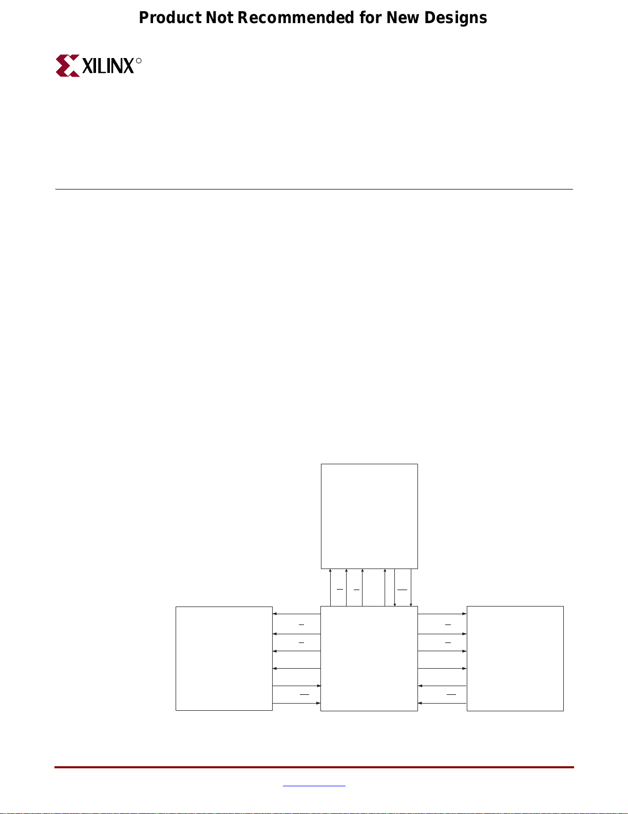
Figure 1-1 shows a simplified block diagram of the ML365 memory interfaces.
QDR II SRAM
1M x 36
FBGA 165
4-Word Burst
C,
QDR II SRAM
1M x 36
FBGA 165
4-Word Burst
(36-bits)
D (36-bits)
C, C
K, K
Addr, Ctrl
Q (36-bits)
CQ, CQ
D
Addr,
K,
C
Ctrl
K
Virtex-II Pro FPGA
XC2VP20FF1152-6
CQ,
CQ
Q
(36-bits)
D (36-bits)
Addr, Ctrl
Q (36-bits)
C, C
K, K
CQ, CQ
QDR II SRAM
1M x 36
FBGA 165
4-Word Burst
ug124_01_062204
Figure 1-1: Simplified Block Diagram of Memory Board Interface
ML365 Virtex-II Pro QDR II SRAM Mem. Board www.xilinx.com 11
UG066 (v1.0) June 29, 2004 1-800-255-7778
Page 12
Features
Product Not Recommended for New Designs
The ML365 demonstrates a 36-bit interface to a 36 MByte, 200 MHz QDR II SRAM
component. There are thr ee independent 36-bit interfaces on the board; one on the le ft side
of the FPGA, the second on the right side of the FPGA, and the third on top of the FPGA.
The key features of the ML365 are summarized as follows:
• One Virtex-II Pro FPGA (XC2VP20FF1152)
• Three QDR II SRAM Components (Samsung K7R323684M or NEC UPD44165364F5)
♦ 18 MBytes
♦ 36-bit Data interface
• Three separate controllers for each 36-bit memory interface
• Characterized 200 MHz clock operation for interfaces A (interface to the FPGA on the
right side, U5) and B (interface to the FPGA on the left side, U11)
• One additional memory interface on the top banks of the FPGA (interface C, U12)
ML365 Virtex-II Pro QDR II SRAM Mem. Board www.xilinx.com 12
UG066 (v1.0) June 29, 2004 1-800-255-7778
Page 13
Product Not Recommended for New Designs
R
Architecture
This chapter provides functional descriptio ns of the major blocks wi thin the ML365 board
design. For additional detailed information on the design, refer to the schematics, which
are located at http://www.xilinx.com/bvdocs/userguides/ug06
ML365 Board Block Diagram
Figure 2-1 shows a block diagram of the ML365 board. Refer to “Block Descriptions” for
additional information on the major blocks.
Chapter 2
6.zip.
RS-232
Serial
Por t
On / Off
Switch
DC 5V
Input Jack
FPGA
Reset
PROG
QDR II SRAM
Mode
DIP
SW
1M x 36
SMA
QDR II SRAM
1M x 36
XC2VP20
FF1152C
Clock
250 MHz
SMA
USER1
Switch
USER2
Switch
QDR II SRAM
Clock
200 MHz
GPIO Header
1M x 36
USER1
LED
USER2
LED
TPS54810
1.8V, 8A
Regulator
SYSTEM ACE
Controller
TQFP144
JTAG
Jumpers
SelectMap
Header
XCONFIG
Header
SystemAce
Reset
JTAG
Header
JTAG
Parallel
PC-IV
Por t
SystemAce
File Select
Rotary Switch
SEIKO 1X16
LCD Display
L167100J000
PT5502N
2.5V, 3A
Regulator
PT5505N
1.5V, 3A
Regulator
PT5501N
3.3V, 3A
Regulator
ug066_c2_01_060804
Figure 2-1: ML365 Board Block Diagram
ML365 Virtex-II Pro QDR II SRAM Mem. Board www.xilinx.com 13
UG066 (v1.0) June 29, 2004 1-800-255-7778
Page 14

Product Not Recommended for New Designs
R
Block Descriptions
This section describes the major blocks of the ML365 board.
FPGA
The ML365 uses a Xilinx XC2VP20FF1152C-6 Virtex-II Pro device. This device is packaged
in a 1152-pin BGA package with a -6 speed grade. Refer to Appendix 2, “FPGA Pinout,”for
a complete pinout of the Virtex-II Pro device.
Memories
The ML365 board supports three types of memories in two speed grades.
QDR II SRAM (U5, Banks 6 and 7)
The QDR II SRAM component connected to FPGA I/O banks 6 and 7 is a 165-pin, 200 MHz
Samsung K7R323684M or NEC UPD44165364F5 SRAM in a Ball Grid Array package. This
component has a 36-bit wide data interface.
Chapter 2: Architecture
QDR II SRAM (U11, Banks 2 and 3)
The QDR II SRAM component connected to FPGA I/O banks 2 and 3 is a 165-pin, 200 MHz
Samsung K7R323684M or NEC UPD44165364F5 SRAM. This component has a 36-bit wide
data interface.
QDR II SRAM (U12, Banks 0 and 1)
The QDR II SRAM component connected to FPGA I/O banks 0 and 1 is a 165-pin, 250 MHz
Samsung K7R323684M or NEC UPD44165364F5 SRAM. This component has a 36-bit wide
data interface.
RS232 (J5)
The ML365 board provides an RS232 serial interface using a Maxim MAX3316ECUP
device. The maximum speed of this device is 460 Kb/s. The RS232 interface is accessible
through a male DB9 serial connector.
Clocks
The ML365 board has 200 MHz and 250 MHz LVPECL (2.5 V) clock oscillators on board. It
also has two SMA connectors for external differential clock inputs.
200 MHz LVPECL Clock (Y1)
The LVPECL clock is an Epson EG-2121CA-200 MHz oscillator with a differential output.
The oscillator runs at 200 MHz ± 100 PPM with an operating voltage of 2.5 V ± 5%. It is
terminated at the FPGA with a 50 ohm resistor. FPGA pins AH17 and AJ17 in Bank 4 serve
as the OSC_200M_N and OSC_200M_P inputs, respectively.
250 MHz LVPECL Clock (Y2)
The LVPECL clock is an Epson EG-2121CA-250 MHz clock oscillator with a differential
output. This oscillator runs at 250 MHz ± 100 PPM with an operating voltage of 2.5 V ± 5%.
14 www.xilinx.com ML365 Virtex-II Pro QDR II SRAM Mem. Board
1-800-255-7778 UG066 (v1.0) June 29, 2004
Page 15

Product Not Recommended for New Designs
Block Descriptions
SMA Clock Connectors
User I/Os
GPIO (P19)
R
FPGA pins AK17 and AL17 in Bank 4 serve as the OSC_250M_N and OSC_250M_P inputs,
respectively.
Two SMA connectors are provided for the input of an off-board differential clock. The
traces from the SMAs are run as a pair to the FPGA where they are terminated with a
50 ohm resistor. AK18 serves as the EXT CLK1 _P input, and AL18 serves as the
EXTCLK1_N input for the SMA connector pair.
This subsection describes the devices that connect to the User I/Os of the ML365 board.
The ML365 board contains 16 General-Purpose I/Os (GPIOs) that are accessible thr ough a
2 x 16 .100" pin header (P19). The odd-numbered pins on each header are connected to an
FPGA pin, and the even-numbered pins on each header are connected to GND (refer to
Table 2-1). The GPIO header pins are accessed through I/Os in Bank 0. The header pins
each have a pull-down resistor of 51 ohms.
Table 2-1: GPIO Header Pins
GPIO Header Pin # FPGA I/O Pin
G1 AL13 G2
G3 AL12 G4
G5 AD16 G6
G7 AE16 G8
G9 AM14 G10
G11 AM13 G12
G13 AF16 G14
G15 AG16 G16
G17 AH15 G18
G19AJ15G20
G21AD17G22
G23 AE17 G24
G25 AH16 G26
GPIO Header Pin #
Ground Connections
G27AJ16G28
G29AK16G30
G31 AF17 G32
ML365 Virtex-II Pro QDR II SRAM Mem. Board www.xilinx.com 15
UG066 (v1.0) June 29, 2004 1-800-255-7778
Page 16
Product Not Recommended for New Designs
R
DIP Switch (SW3)
One 3-position DIP switch (SW3) is connected to the FPGA I/O as shown in Table 2-2.
These switches are used to set the FPGA configuration mode pins M0, M1, and M2.
Table 2-2: DIP Switch Connections
DIP Switch Input FPGA I/O Pin #
DIP1 AF26 (M0)
DIP2 AE26 (M1)
DIP3 AE25 (M2)
LEDs
Eleven surface-mounted blue LEDs are installed as status indicators. Refer to Table 2-3,
Table 2-4, and Table 2-5.
Chapter 2: Architecture
Table 2-3: Power-On Status
Status Indication FPGA I/O Pin #
5.0V on D9
2.5V on D7
3.3V on D5
1.8V on D8
1.5V on D6
Table 2-4: FPGA Configuration Status
Configuration INIT D3
Configuration DONE D4
Table 2-5: SystemAce Configuration Status
System Ace LEDs
User LEDs
Error D2
Status D1
USER1 AF15
USER2 AE15
16 www.xilinx.com ML365 Virtex-II Pro QDR II SRAM Mem. Board
1-800-255-7778 UG066 (v1.0) June 29, 2004
Page 17

Product Not Recommended for New Designs
Block Descriptions
Push Buttons
Rotary Switch
Power On or Off Slide Switch
R
The ML365 board contains five momentary push buttons. Their functions are as follows:
• Program the FPGA
• Reset FPGA
• Reset SystemAce
• USER1
• USER2
The ML365 board contains one eight-position rotary switch used to select the SystemAce
file address. One of eight configuration fi le images is loaded f r om the Compact Flash card
present in the socket.
The power on or off slide switch is a DPST s lide switch used to apply 5V input power to the
board.
Jumper Settings
Table 2-6 list s the jumper settings for the complete PCB.
Table 2-6: Jumper Settings
Pin # Purpose
P6 QDR II U5 DLL enable DLL enable DLL bypass
P7 QDR II U5 ZQ select Minimum Z mode 0.2RQ = 50 ohm
P20 QDR II U11 DLL enable DLL enable DLL bypass
P21 QDR II U11 ZQ select Minimum Z mode 0.2RQ = 50 ohm
P22 QDR II U12 DLL enable DLL enable DLL bypass
P23 QDR II U 12 ZQ select Minimum Z mode 0.2RQ = 50 ohm
P2 System Ace On = Disable after reset
Grounded I/Os
Unused I/Os are connected to GND in all FPGA banks. This was done to improve power
dissipation and SSO ground bounce. Users must not drive any unused I/Os that are
connected to GND.
Jumper Position
1 - 2 2 - 3
Off = Enable after reset
ML365 Virtex-II Pro QDR II SRAM Mem. Board www.xilinx.com 17
UG066 (v1.0) June 29, 2004 1-800-255-7778
Page 18
Product Not Recommended for New Designs
R
Liquid Crystal Display
The Seiko L167100J000 Liquid Crystal Display (LCD) is a 5V, 1-line X16 character display
without a backlight. The LCD is connected to the PCB using two rows of 1 x 16 pin SIP
headers placed 31 mm. apart. The LCD interfaces uses bank 5 of the FPGA. The LCD pin
descriptions and FPGA pinouts are listed in Table 2-7.
Table 2-7: LCD Pin Descriptions and PFGA Connections
Symbol Function FPGA Pin #
Chapter 2: Architecture
V
SS
V
DD
V
O
Power supply (GND) N/A
Power supply (+5V) N/A
Contrast adjustment N/A
RS Register selection AF22
R/W Read / Write selection AG22
E Read / Write enable AE22
DB (0-7) Data bus AF25 (DB0), AL28, AM28, AE24,
AF24, AG25, AH25, AK27 (DB7)
The information needed to control the LCD panel is provided in the following figures and
tables. Figure 2-2 shows the LCD write timing diagram, and Table 2-8 lists the LCD write
timing parameters.
Table 2-9 shows the instruction codes for the LCD. Figure 2-3 shows the Display
Initialization Sequence, and Figure 2-7, the LCD panel character set. For complete
information, refer to the manufacturer’s data sheet.
Write Cycle for the LCD
Reading from the LCD panel memory is not implemented on this demonstration board.
RS
R / W
DB[7:0]
t
AS
PW
EH
E
t
ER
t
DSW
t
t
CYC
EF
t
AH
t
H
E
ug066_c2_02_060704
Figure 2-2: LCD Write Timing Diagram
18 www.xilinx.com ML365 Virtex-II Pro QDR II SRAM Mem. Board
1-800-255-7778 UG066 (v1.0) June 29, 2004
Page 19

Product Not Recommended for New Designs
Block Descriptions
R
Table 2-8: LCD Write Timing Parameters
Enable pause width / High Level PW
Address setup time / RS, R/W - E t
Display Commands
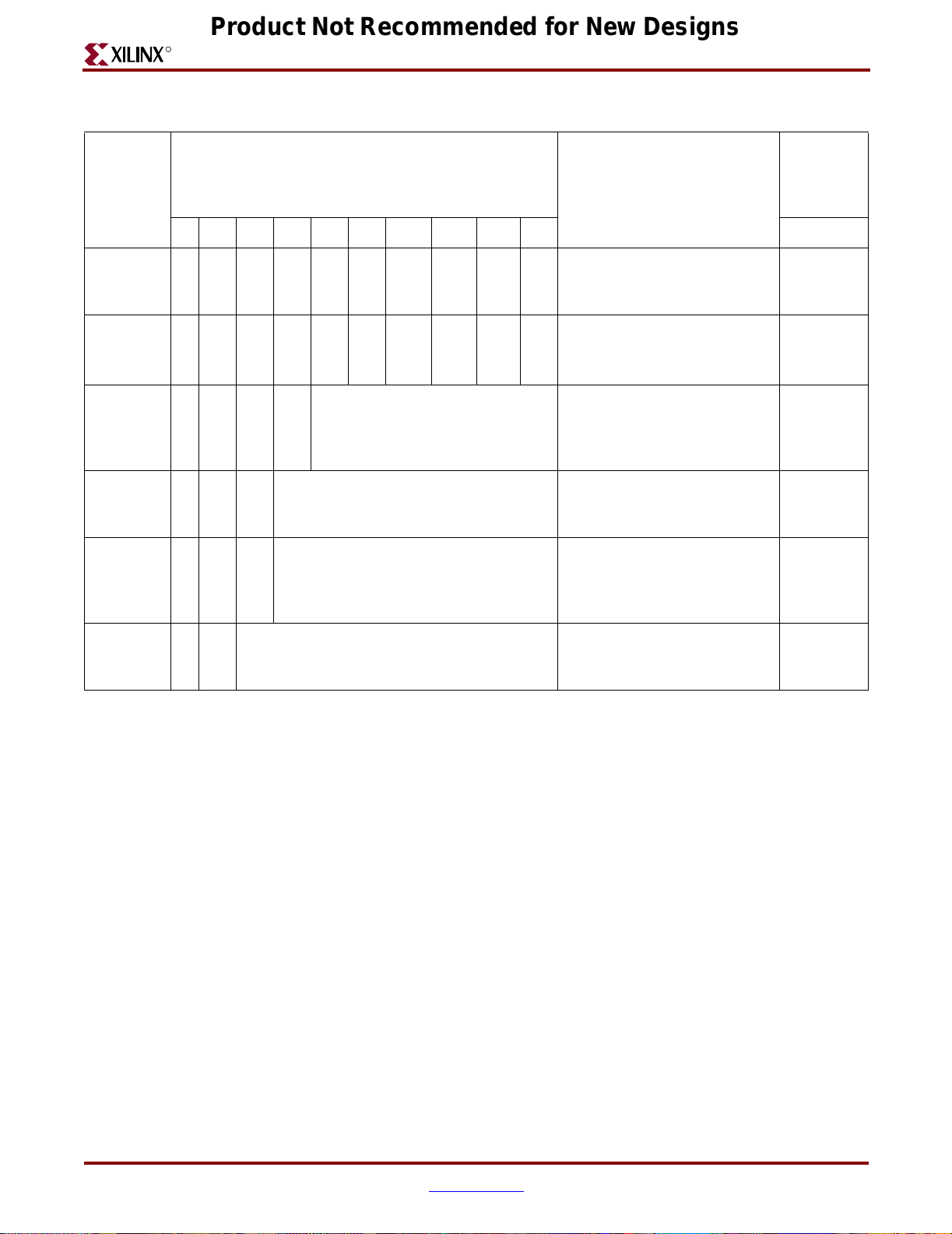
Table 2-9 provides display commands or instruction code for the LCD. Refer to the Table
Notes for additional information.
Table 2-9: Instruction Code
Instruction
Item Symbol
Enable cycle time t
Enable rise and fall time t
Address hold time t
Data setup time t
Data hold time t
Code
Standard
Unit
Minimum Maximum
E500 ns
CYC
230 ns
20 ns
40 ns
10 ns
80 ns
10 ns
ER
DSW
, t
AS
AH
H
EH
EF
Maximum
Execution
Description
(Notes 2 and 3)
Time
(Note 1)
Clear
Display
Return
Home
Entry
Mode
Set
Display
On/Off
Control
RS R/W DB7 DB6 DB5 DB4 DB3 DB2 DB1 DB0
000000 0 0 0 1Clears entire display and sets
Data Display RAM (DDR)
address 0 in the address
counter.
000000 0 0 1 *Sets DDR address0 in the
address counter. Also returns
display being shifted to
original position. DDR
contents remain unchanged.
000000 0 1I/DSSets cursor move direction
and specifies shift of display.
These operations are
performed during data write
and read.
000000 1 D CBSets ON/OFF of entire
display (D), cursor ON/OFF
(C), and blink of cursor
position character (B).
µs -
82
1.64 ms
µs -
40
1.6 ms
µs –
40
1.64 ms
µs
40
ML365 Virtex-II Pro QDR II SRAM Mem. Board www.xilinx.com 19
UG066 (v1.0) June 29, 2004 1-800-255-7778
Page 20
Product Not Recommended for New Designs
R
Table 2-9: Instruction Code
Instruction
RS R/W DB7 DB6 DB5 DB4 DB3 DB2 DB1 DB0
Code
Chapter 2: Architecture
Description
(Notes 2 and 3)
Maximum
Execution
Time
(Note 1)
Cursor or
Display
Shift
Function
Set
Set
CG RAM
Address
Set
DD RAM
Address
Read
Busy Flag
and
Address
Write Data
to CG
or DDR
000001S/CR/L* *Moves cursor and shifts
40 µs
display without changing
DDR contents.
00001DLN F * *Sets interface data length (DL),
40
number of display lines (L),
and character fonts (F).
0001 A
CC
Sets Character Generator
40 µs
RAM (CGR) address. CGR
data is sent and received after
this setting.
00 1 A
DD
Sets DDR address. CGR data
40 µs
is sent and received after this
setting.
01BF A
C
Reads Busy flag (BF)
1 µs
indicating internal operation
is being performed and reads
address counter contents.
1 0 Write Data Writes data into DDR or CGR. 40
µs
µs
*Not applicable
Notes:
1.Maximum execution time is when f
changes.
2.DD RAM: Display data RAM
CG RAM: Character generator RAM
A
: CG RAM address
CG
A
: DDR address - corresponds to cursor address
DD
A
: Address counter used for both DDR and CG RAM address
C
I/D = 1: Increment or I/D = 0: Decrement
S = 1: Display shi ft or S = 0: No Display shift
D=1: Display ON or D=0: Display OFF
C = 1: Cursor ON or C = 0: Cursor OFF
B = 1: Blink ON or B = 0: Blink OFF
S/C = 1: Display shift or S/C = 0: Cursor move
R/L = 1: Shift to the right or R/L = 0: Shift to the left
DL = 1: 8 bits or DL = 0: 4 bits
N=1: 2lines
F=0: 5x 7 dots
BF = 1: In ternally operatin g or BF = 0: Can accept instruction
cp
or f
is 250 kHz. Execution time changes when frequency
osc
20 www.xilinx.com ML365 Virtex-II Pro QDR II SRAM Mem. Board
1-800-255-7778 UG066 (v1.0) June 29, 2004
Page 21
Product Not Recommended for New Designs
Block Descriptions
R
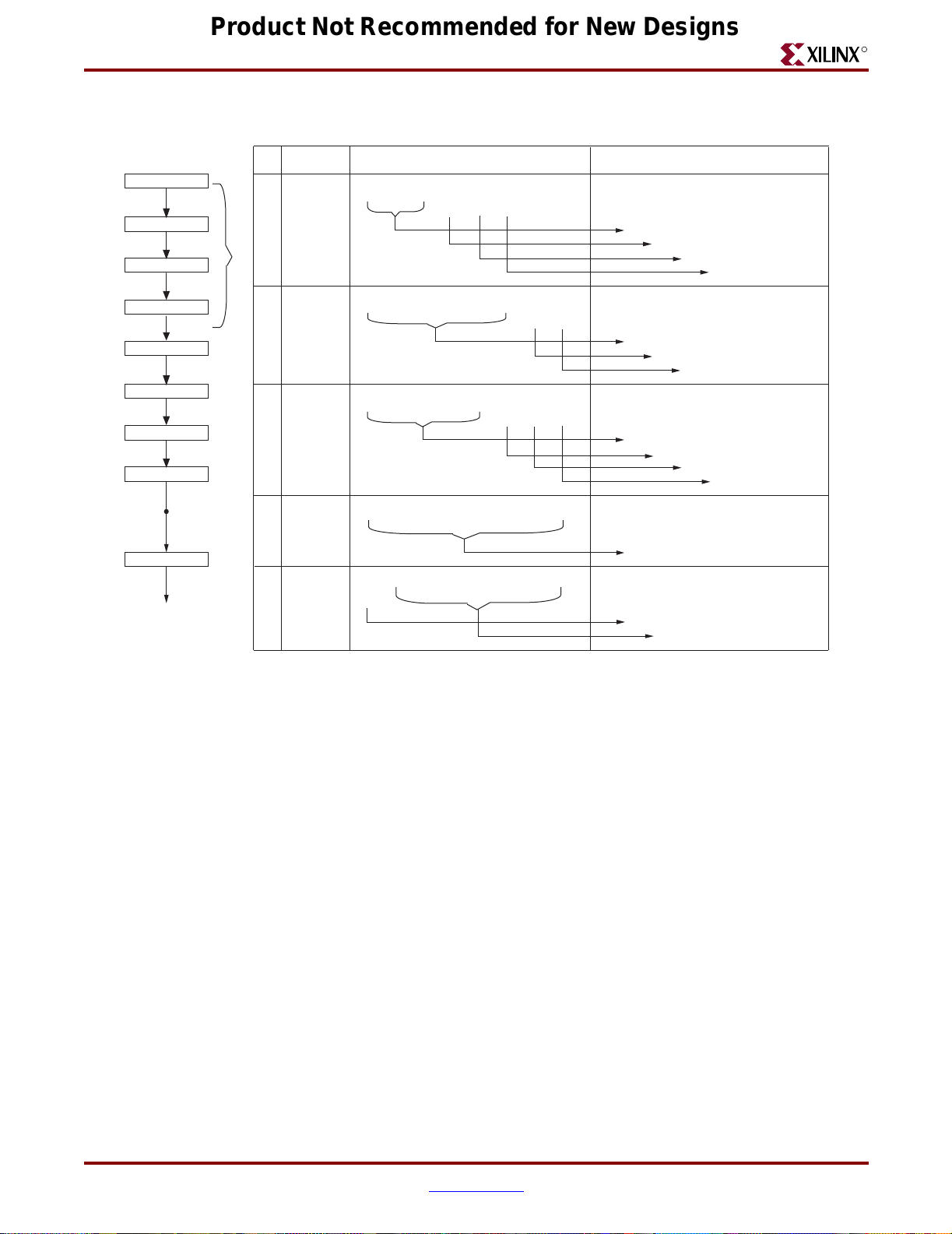
Initialization
Flow Chart
Power On
≥ 15 mS
38 (Hex)
≥ 4.1 mS
38 (Hex)
≥ 100 uS
38 (Hex)
≥ 40 uS
38 (Hex)
≥ 40 uS
06 (Hex)
≥ 40 uS
0E (Hex)
≥ 40 uS
01 (Hex)
≥ 1.64 uS
End of
Initialization
80 (Hex)
≥ 40 uS
Hex Code D
R
E
S
E
T
S
E
Q
U
E
N
C
E
(1)
(2)
38 (Hex)
06 (Hex)
(1)
(2)
(3)
0E (Hex)
(3)
(4)
(4)
01 (Hex)
(5)
80 (Hex)
(5)
7D6D5D4D3D2D1D0
0
01
0000
0
00
1
00000
0
00
1
1000
00
1
0
0000
11
1
1
Function Set
8-bit Data Length
2 Line
5 x 7 Dot Format
Entry Mode Set
Increment One
No Shift
000
Display On/Off Control
Display On
Cursor On
Blink Off
1
Display Clear
Figure 2-3: Display Initialization Sequence
DD RAM Address Set
1st Digit
ug066_c2_03_060804
ML365 Virtex-II Pro QDR II SRAM Mem. Board www.xilinx.com 21
UG066 (v1.0) June 29, 2004 1-800-255-7778
Page 22
Product Not Recommended for New Designs
R
Chapter 2: Architecture
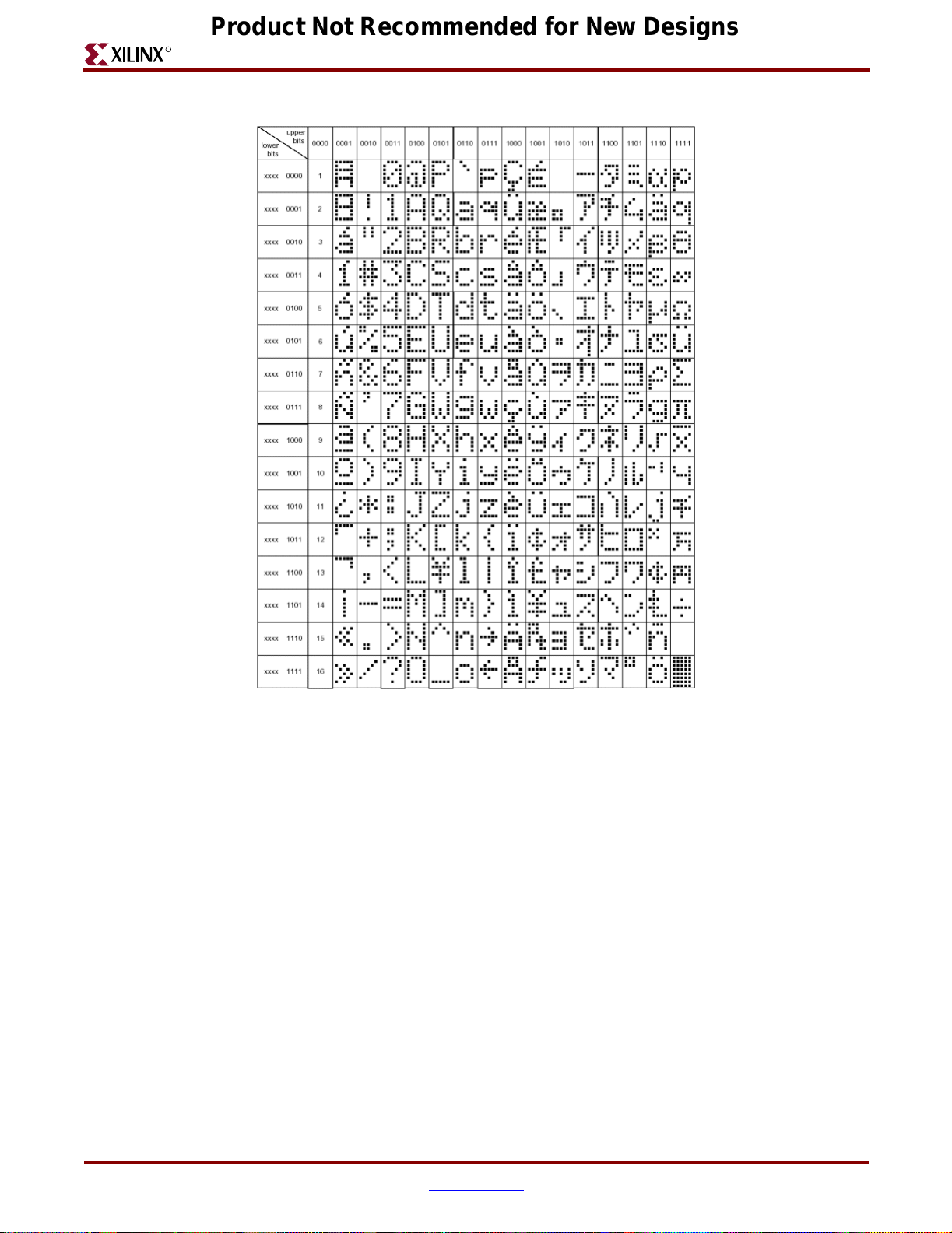
Figure 2-4: LCD Panel Character Set
ug066_c2_04_060704
22 www.xilinx.com ML365 Virtex-II Pro QDR II SRAM Mem. Board
1-800-255-7778 UG066 (v1.0) June 29, 2004
Page 23
Power
Power
Product Not Recommended for New Designs
Power Distribution
The ML365 board uses a 5V +/- 10% input voltage source to generate all the on-board
voltages (1.5V, 1.8V, 2.5V, and 3.3V).
Input Voltage
The input voltage is specified at 5 V @ 6.5 A. The recommended power supply is a CUI Inc.
DTS050650UTC-PSP-SZ. The jack used is a 2 mm. barrel jack. The slide switch turns the
power on or off. Four regulators on the board provide different voltages required by
various components on the board.
3.3 V Generation
The Texas Instruments PT5501N voltage regulator generat es the 3.3 V @ 3 A power. This
power regulator is packaged in a 5-pin, thermally-efficient copper case that is solderable,
and provides the auxiliary supply for some of the FPGA I/Os (V
CCO
).
R
2.5 V Generation
The Texas Instruments PT5502N voltage regulator generat es the 2.5 V @ 3 A power. This
power regulator is packaged in a 5-pin, thermally-ef ficient copper case that is solderable. It
supplies the clock oscillators, System Ace device, LCD Display unit, and for some of the
FPGA I/Os (V
CCAUX
).
1.8 V Generation
The Texas Instruments TSP54810 voltage regulator generates the 1.8 V @ 8 A power. This
power regulator has a thermally-enhanced 28-pin TSSOP package, and supplies the
memory devices.
1.5 V Generation
The Texas Instruments PT5505N voltage regulator generat es the 1.5 V @ 3 A power. This
power regulator is packaged in a 5-pin, thermally-efficient copper case that is solderable,
and provides the core voltage to the FPGA (V
CCINT
).
ML365 Virtex-II Pro QDR II SRAM Mem. Board www.xilinx.com 23
UG066 (v1.0) June 29, 2004 1-800-255-7778
Page 24

Product Not Recommended for New Designs
R
FPGA Configuration
The demonstration board FPGA programming options are very flexible (refer to the
following five configuration modes). For a detailed explanation of the basic Virtex-II
configurations, refer to the Virtex-II Platform FPGA User Guide. The five Virtex-II
configuration modes are:
• Master Serial mode (not used on QDR II Demo Board)
• Slave Serial / SystemAce mode (QDR II Demo Board default)
• Master SelectMap mode
• Slave SelectMap mode
• JT AG mode
Selecting the Configuration Mode
The FPGA programming modes are set with the mode lines (M0, M1, M2) by means of the
3-pole DIP switch (SW5). Table 2-10 shows the programming modes.
Chapter 2: Architecture
Table 2-10: Configuration Modes Supported on the QDR II SRAM Demonstration Board
Mode M2 M1 M0 CCLK Data Width Data DOUT
Master Serial
Slave Serial 1 1 1 In 1 Yes
SystemAce
Master SelectMap 011 Out 8 No
Slave SelectMap 110 In 8 No
JTAG 101 N/A 1 No
(1)
(2)
1. Not used on QDR II Demonstration Board.
2. SystemAce is a Slave Serial configuration mode, and is the default for the QDR II Demonstration Board.
An LED on the Done pin adds a visual aid to detect a good FPGA configuration. If the LED
is “on”, the FPGA configuration is complete.
000 Out 1 Yes
111 N/A N/A N/A
Serial Configuration
The Virtex-II is programmable in serial mode in one of two ways:
Master Serial Mode
This mode is not used in the QDR II Demonstration Board.
Slave Serial Mode
In Slave Serial Mode, the FPGA CCLK pin is driven by an external source. The FPGA is
configured by loading one bit per CCLK cycle in the DIN pin.
24 www.xilinx.com ML365 Virtex-II Pro QDR II SRAM Mem. Board
1-800-255-7778 UG066 (v1.0) June 29, 2004
Page 25

Product Not Recommended for New Designs
FPGA Configuration
SystemAce Configuration (Default Mode)
R
SystemAce is a Slave Serial configuration mode, and is the default mode for the QDR II
Demonstration Board.
If the SystemAce Controller (U2) detects a Compact Flash card present in sock et P2, it
attempts to load a configuration file from the Compact Flash card into the FPGA.
Table 2-11 shows the allowable correct jumper positions.
Table 2-11: Jumper Positions for SystemAce Configuration
Pins Jumpered Function
P1.4 to P113 TCK from SystemAce connected to TCK input of the FPGA
P1.7 to P114 TMS from SystemAce connected to TMS input of the FPGA
P1.5 to P1.6 SystemAce TDO connected to the TDI input of the FPGA
1. Recommended SW5 switch setting for the SystemAce mode is 111; refer to Table 2-10.
SelectMap Configuration
The Virtex-II FPGA is programmable us ing SelectMap, a parallel configuration mode. In
this mode, two possibilities of programming exist:
• Master Mode: FPGA delivers the CCLK download clock
• Slave Mode: FPGA must receive the CCLK clock from the external device
The demonstration board can be programmed in both modes using the SelectMap
connectors; P99 and P111. The FPGA on the demonstration board can be programmed in
slave mode using a MultiLINX cable, or in Master mode when an external device is
plugged into these connectors.
The SelectMap connector P99 carries FPGA bits [7:0]. When SelectMap is not used, the
SelectMap connector pins can also be used as normal I/O.
Figure 2-5 shows the layout of the SelectMap connectors P99 and P111.
ML365 Virtex-II Pro QDR II SRAM Mem. Board www.xilinx.com 25
UG066 (v1.0) June 29, 2004 1-800-255-7778
Page 26
Product Not Recommended for New Designs
R
Chapter 2: Architecture
FPGA CS#
FPGA RFWR#
P99
1
3
5
7
9
11 12
13 14
15
17
SelectMAP Header
2
4
6
8
10
16
18
FPGA BUSY
FPGA D0
FPGA D1
FPGA D2
FPGA D3
FPGA D4
FPGA D5
FPGA D6
FPGA D7
1
2
3
4
5
6
7
8
9
Header 9
Figure 2-5: SelectMap Connectors P99 and P111
P111
5V
GND
CCLK
DONE
DIN
PROG
INIT
ug066_c2_05_060804
26 www.xilinx.com ML365 Virtex-II Pro QDR II SRAM Mem. Board
1-800-255-7778 UG066 (v1.0) June 29, 2004
Page 27
Product Not Recommended for New Designs
FPGA Configuration
JTAG Configuration
The Virtex-II FPGA is programmable in JTAG mode. The JTAG chain contains two onboard devices (FPGA and SystemAce).
The JT AG input connector is P103, wir ed to the TSTCFG pins of the Sys temAce Contr oller
U2. The JT AG input connector is the start of the JT AG chain. The configuration output port
of the SystemAce Controller is wired to the FPGA via P1, P113, and P114 pins as shown in
Table 2-11. The FPGA can be isolated from the JTAG chain by removing the jumper blocks
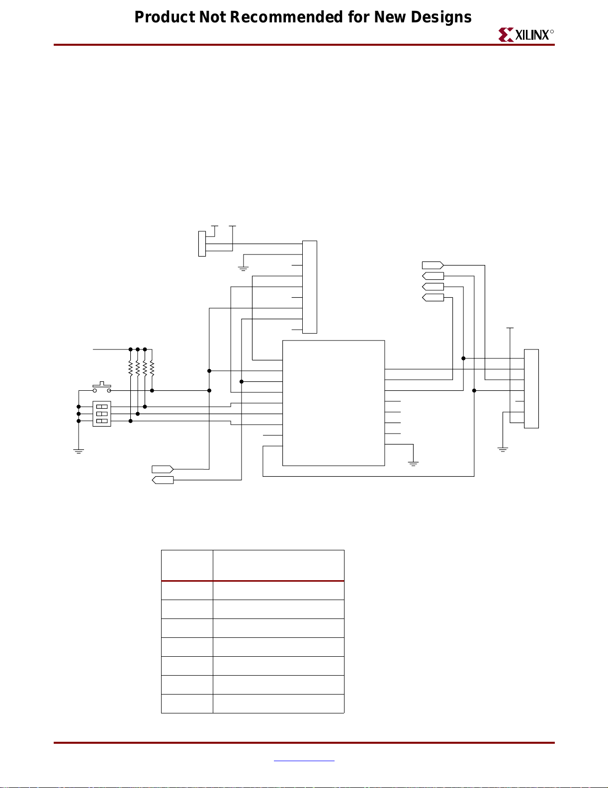
from the P1 pins as specified in Table 2-11. Figure 2-6 shows how to build the JTAG chain,
and Table 2-12 shows the connections for the JTAG connector P1.
+5 V +2.5 V
P111
1
2
P26
PROG_B
CCLK
DIN
PROG
INIT
3
4
5
6
7
8
9
SYSACE_TDO
TCK
TMS
FPGA_TDO
+3.3 V
R
+3.3 V
Pushbutton
SW6
1
DIP Switch
SW5
SYSACE_CFGPROG#
SYSACE_CFGINIT#
10K
Resistors (4)
AH8
CCLK
D30
PROG_B
AL5
IO_L01P_4/INIT_B
AJ7
DONE
AH27
M0
AJ28
M1
AK29
M2
F29
HSWAP_EN
F7
TCK
U1I
XC2V3000
Figure 2-6: SystemAce and JTAG Connectors
Table 2-12: JTAG Connector Pins (P1)
Pin
Number
Function
1 3.3 Volts
2GND
3N/C
TDI
TDO
TMS
PWRDWN_B
DXN
DXP
VBATT
RSVD
D5
F6
AK6
F28
G27
C4
G8
FPGA_TDIC31
FPGA_TDO
TMS
TDO
TCK
ug066_c2_06_062804
P1
7
6
5
4
3
2
1
4TCK
5TDO
6FPGA_TDI
7TMS
ML365 Virtex-II Pro QDR II SRAM Mem. Board www.xilinx.com 27
UG066 (v1.0) June 29, 2004 1-800-255-7778
Page 28

Product Not Recommended for New Designs
R
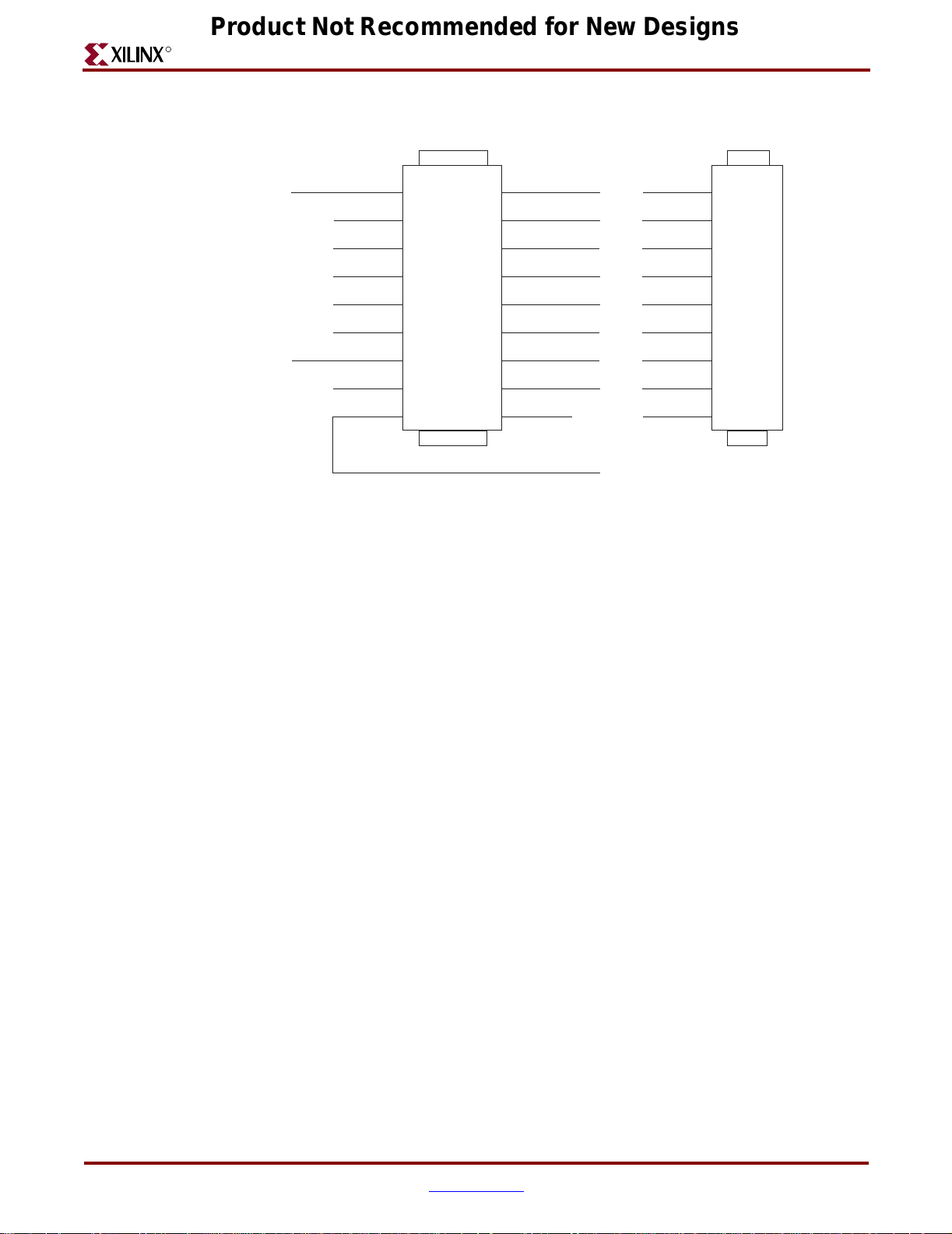
Figure 2-7 shows the JTAG connector P103.
Chapter 2: Architecture
NC
NC
NC
1
2
3
4
5
P103
6
7
8
9
3.3V
GND
TCK
TDO
TDI
TMS
ug124_07_0603_04
Figure 2-7: JTAG I/O Connector P103
28 www.xilinx.com ML365 Virtex-II Pro QDR II SRAM Mem. Board
1-800-255-7778 UG066 (v1.0) June 29, 2004
Page 29
Product Not Recommended for New Designs
R
Electrical Requirements
Power Consumption
Table 3-1 lists the operating voltages, maximum currents, and power consumption used by
the ML365 board devices. Refer to Appendix 1, “Related Documentation,” for more
information on the source material.
Table 3-1: ML365 Power Consumption
Chapter 3
1
Voltag e
(V)
1.8 7236 1 3 Virtex-II Pro User Guide
Device Quantity
Total Available Power
Power Supply 1 5 6500 32.5
FPGA Power (Based on Design)
FPGA (XC2VP20-6 FF1152) 1 6.87 Power Estimator Tool
Board Power
Static Power-on Termination
Resistors (Split 100 ohms)
QDR SRAM (108-bit interface) 3 1.8 800 4.32 Samsung QDR SRAM Data Sheet
200 MHz LVPECL Clock
Oscillator
16-pin GPIO Header 2 2.6 160 .42 Average 10 mA * 16 pins
LEDs 11 — — 0.5 LED Circuits
DIP Switch 1 — — .06 Eight 3.3 kohm pullups
RS232 Serial Port 1 3.3 40 0.13 Maxim MAX3316ECUP Data Sheet
LCD — 2.5/3.3 100 0.33 LCD Datasheet
402
2 4 80 0.64 EPSON EG2121CA Data Sheet
Current
(mA)
Power
(W)
Source
System Ace Compact Flash — 2.5/3.3 150 .049 SystemACE Datasheet
Worst Case Power Consumption: 23.0
1. The resistor count is distributed as follows per devices, and multiplied by the number of devices (3):
- data bus D: 36 (x2 (split termination))
- clocks: CQ, C, K: 6 (x2 (split termination) )
- address bus A: 18 (x2 (split termination))
- R_n_int: 1 (x2 (split termination))
- Control signals: 6 (x2 (split termination))
ML365 Virtex-II Pro QDR II SRAM Mem. Board www.xilinx.com 29
UG066 (v1.0) June 29, 2004 1-800-255-7778
Page 30

Product Not Recommended for New Designs
FPGA Internal Power Budget
The following tables show the power consumption values inside the FPGA based on the
complete QDR design. These results are derived using the Xilinx Power Estimator tool.
Block Select RAM, Block Multiplier, Processor, and MGT Power tables are not included in
this section as they are not used in this application.
• Table 3-2, “XC2VP20FF1152 Estimated Power Consumption,” page 30
• Table 3-3, “XC2VP20FF1152 Temperature Specifications,” page 30
• Table 3-4, “Device Quiescent Power,” page 30
• Table 3-5, “CLB Logic Power,” page 31
• Table 3-6, “D ig ital Clock Manager Power,” page 31
• Table 3-7, “Input/Output Power,” page 31
Table 3-2: XC2VP20FF1152 Estimated Power Consumption
Parameter Value Units
Total Estimated Design Power 6500 mW
Estimated Design VCC
Estimated Design VCC
Estimated Design VCCO 3.3 V Power 100 mW
Estimated Design VCCO 2.5 V Power 173 mW
Estimated Design VCCO 1.8V Power 7859 mW
Estimated Design VCCO 1.5 V Power 0 mW
Estimated Design VCCO 1.2 V Power 0 mW
Table 3-3: XC2VP20FF1152 Temperature Specifications
Parameter Value Units
Ambient Temperature 25 °C
Air Flow 0 LFM
Junction Temperature 107 °C
Table 3-4: Device Quiescent Power
VCC
Subtotal (mW) VCC
INT
1.5 V Power 3500 mW
INT
2.5 V Power 417 mW
AUX
Subtotal (mW)
AUX
450 417
ML365 Virtex-II Pro QDR II SRAM Mem. Board www.xilinx.com 30
UG066 (v1.0) June 29, 2004 1-800-255-7778
Page 31

Product Not Recommended for New Designs
Table 3-5: CLB Logic Power
Name
Frequency
(MHz)
Tot al
Number
of CLB
Slices
Tot al
Number of
Flip/Flop or
Latches
Total Number
of Shift
Register
LUTs
Total
Number of
Select RAM
LUTs
Average
Toggle
Rate
%
Amount of
Routing
Used
VCC
Subtotal
(mW)
User Module 1 200 1299 1302 0 544 40% High 1220
User Module 2 0 0 0 0 0 0% Low 0
Total 1220
Table 3-6: Digital Clock Manager Power
Name
Clock Input Frequency
(MHz)
DCM Frequency Mode VCC
Subtotal (mW)
INT
User DCM 1 200 Low 6
User DCM 2 200 Low 6
Total 12
Table 3-7: Input/Output Power
Tot al
Name
CLK200 200 LVDS_25 1 0 100% 100% 15 DDR 2 8
CLK200_N 200 LVDS_25 1 0 100% 100% 35 DDR 2 8
Frequency
(MHz)
I/O Standard
Type
Number
of
Inputs
Number
Outputs
Tot al
of
Average
Tog gle
IOB
Rate
%
Average
Output
Enable
Rate
%
Average
Output
Load
(pF)
IOB
Registers
VCC
INT
Subtotal
(mW)
VCCO
Subtotal
INT
(mW)
GPIO 200 LVDCI_ 25 (50) 0 16 10% 100% 35 DDR 14 157
D/mem_R_n_ext 200 HSTL_II (1.8v) 0 111 25% 100% 35 DDR 11 752
Q/mem_R_n_int 200 HSTL_II_DCI (1.8v) 111 0 25% 0% 35 DDR 258 3662
Mem Addr/Control 200 HSTL_II_DCI (1.8v) 0 66 10% 100% 35 SDR 18 2431
Mem K/C 200 HSTL_II_DCI (1.8v) 0 12 25% 100% 35 DDR 13 536
Mem CQ 200 HSTL_II_DCI (1.8v) 6 0 25% 0% 35 DDR 25 260
A_R/W, C_R/W 200 HSTL_II (1.8v) 0 12 10% 100% 35 SDR 1 41
Total 344 7859
31 www.xilinx.com ML365 Virtex-II Pro QDR II SRAM Mem. Board
1-800-255-7778 UG066 (v1.0) June 29, 2004
Page 32

Product Not Recommended for New Designs
ML365 Virtex-II Pro QDR II SRAM Mem. Board www.xilinx.com 32
UG066 (v1.0) June 29, 2004 1-800-255-7778
Page 33

Product Not Recommended for New Designs
Termination and Transmission Line Summaries
Chapter 4
Signal Integrity Recommendations and Simulations
This chapter provides the following information:
• Summary of the termination schemes for various signals
(refer to “Termination and Transmission Line Summaries,” page 33).
• IBIS simulations and duty cycle measurements (refer to “IBIS Simulations,” page 35).
R
Termination and Transmission Line Summaries
Table 4-1 summarizes the terminations for the three QDR II SRAM components for both
the FPGA and memory.
Table 4-1: QDR SRAM Terminations
Number Signal Drivers at the FPGA Termination at FPGA Termination at Memory
1 Data (D) HSTL_18_C2_DCI No termination 50 ohm pull-up to 0.9 V
2 Data (Q) HSTL_18_C1 No termination No termination
3 Data Strobe (CQ, CQ
4 Clock (K, K
Address (A) HSTL_18_C2 No termination 100 ohm parallel split
5
Control (R
6
) HSTL_18_C2 50 ohm pull-up to 1.3V No termination
, W, BW) HSTL_18_C2 No termination 100 ohm parallel split
) HSTL_18_C2 50 ohm pull-up to 1.3V 50 ohm pull-up to 0.9 V
termination pull-up to
1.8 V
termination pull-up to
1.8 V
ML365 Virtex-II Pro QDR II SRAM Mem. Board www.xilinx.com 33
UG066 (v1.0) June 29, 2004 1-800-255-7778
Page 34

Product Not Recommended for New Designs
R
Chapter 4: Signal Integrity Recommendations and Simulations
Terminations and Transmission Lines for QDR Components
Data and Clock Signals (D, Q, CQ, CQ, and CLK)
For the QDR signals included in the data bus D, the terminations consist of a 50 ohm
parallel termination pulled-up to 0.9 Volts. As DCI is used in the FPGA, no termination is
required.
Use 50 ohm transmission lines with less than ±1% tolerance on
impedance. The recommendations for the transmission line lengths are:
• All the data and clock signals are point-to-point from the FPGA to each QDR
component. The flight time of the signals going to one individual QDR II SRAM
component need to be matched with respect to the other signals with a ±2% tolerance.
• All signals going to the memory component have been matched within a 200 ps.
window. This timing requirement includes the FPGA internal package skew
(available in Appendix 2, “FPGA Pinout”) and the skew between the ball of the FPGA
to the resistor pack as well as the length of the actual trace.
• The IBIS simulation provided in “IBIS Simulations,” page 35 have been processed
using the actual PCB characteristics, from the PCB layout tool and the memory and
FPGA driver IBIS models.
Address and Control Signals (A, R, W, BW)
For the address and control signals, no termination is r equir e d at the FPGA. At memory, a
50 ohm resistor pulled up to 0.9 V is used to terminate the transmission line.
Use 50 ohm transmission lines with ± 5% tolera
components. The recommendations for the transmission line lengths are as follows:
• All the data and clock signals are point-to-point from the FPGA to each QDR
component. The flight time of the signals going to one individual QDR II SRAM
component need to be matched with respect to to the other signals with a ± 2%
tolerance.
• All signals going to the memory component have been matched within a 200 ps.
window. This timing requirement includes the FPGA internal package skew
(available in Appendix 2, “FPGA Pinout”) and the skew between the ball of the FPGA
to the resistor pack as well as the length of the actual trace.
• The IBIS simulation provided in “IBIS Simulations,” page 35 have been processed
using the actual PCB characteristics, from the PCB layout tool and the memory and
FPGA driver IBIS models.
the transmission line
nce from the FPGA to all the memory
34 www.xilinx.com ML365 Virtex-II Pro QDR II SRAM Mem. Board
1-800-255-7778 UG066 (v1.0) June 29, 2004
Page 35

Product Not Recommended for New Designs
IBIS Simulations
IBIS Simulations
This section summarizes the various simulations run on the ML365 Board using IBIS. The
simulations have been completed using the Cadence SPECCTRAQuest tool. These
simulations account for specific PCB characteristics, ensuring high fidelity waveforms. For
each waveform presented in this section, the results of the test conditions are provided.
The simulations have been divided into the following categories:
Data Signal Simulations
R
♦ Data signals from the FPGA to the QDR II SRAM, U11, Component B, Data D,
Bit 4
- Typical Case
- Slow Weak Case
- Fast Strong Case
- Eye Diagram
♦ Data signals from the QDR II SRAM to the FPGA, U11, Component B, Data Q,
Bit 4
- Typical Case
- Slow Weak Case
- Fast Strong Case
- Eye Diagram
Clock Signal Simulations
♦ Clock signals from the FPGA to the QDR II SRAM, U11, Component B
- Typical Case
- Slow Weak Case
- Fast Strong Case
Address and Control Signal Simulations
♦ Address and control signals from the FPGA to the QDR II SRAM Memory
Component
- QDR II SRAM, U11, Component B, Address Bit 4 (Typical, Slow/Weak, and
Fast/Strong Cases)
Notes on the Simulation Results
The provided waveforms show the results of each simulation. The signals in these
waveforms are color-coded:
• Purple signal: T y pical driver
• Green signal: Fast/strong driv er
• Blue signal: Slow/weak driver
For the eye diagram, the typical drivers are used.
ML365 Virtex-II Pro QDR II SRAM Mem. Board www.xilinx.com 35
UG066 (v1.0) June 29, 2004 1-800-255-7778
Page 36

Product Not Recommended for New Designs
R
Data Signal Simulations
All of the data signal simulation use the following test conditions for typical, slow/weak,
and fast/strong cases:
• Topology for data signals: 50-ohm transmission lines
• Transmit:
♦ At the memory: 100-ohm parallel split termination pulled-up to V
(equivalent to a 50-ohm termination pulled up to V
♦ At the FPGA: HSTL_18_C2 drivers
• Receive:
♦ At the FPGA: HSTL_18_C1_DCI receivers (internal termination, VRP, and VRN
pins connected to reference resistors)
Figure 4-1 shows signal terminations for transmitted and received data.
Chapter 4: Signal Integrity Recommendations and Simulations
= 1.8 V
= 0.9V)
ref
V
dd
dd
FPGA
FPGA
QDR II SRAM
QDR II SRAM
ml365_01_061504
Figure 4-1: Signal Terminations for Transmitted and Received Data
36 www.xilinx.com ML365 Virtex-II Pro QDR II SRAM Mem. Board
1-800-255-7778 UG066 (v1.0) June 29, 2004
Page 37

IBIS Simulations
Data Signals from the FPGA to the Memory (HSTL_18_C2 at FPGA)
Product Not Recommended for New Designs
R
The simulations in this subsection test the data signals from the FPGA to the memory.
Simulations were performed for the following cases: typical, slow/weak, and fast/strong
(refer to Figure 4-2).
Figure 4-2: Data Signal Bit 4 from the FPGA to the Memory (Typical Case)
An eye diagram is provided as well (refer to Fi
ML365 Virtex-II Pro QDR II SRAM Mem. Board www.xilinx.com 37
UG066 (v1.0) June 29, 2004 1-800-255-7778
gure 4-3).
Page 38

Product Not Recommended for New Designs
R
Chapter 4: Signal Integrity Recommendations and Simulations
Figure 4-3: Eye Diagram for Data Bit 4 from the FPGA to the QDR II SRAM, U11
38 www.xilinx.com ML365 Virtex-II Pro QDR II SRAM Mem. Board
1-800-255-7778 UG066 (v1.0) June 29, 2004
Page 39

IBIS Simulations
Data Signals from the QDR II SRAM, Component U11 to the FPGA Measured at the FPGA
Product Not Recommended for New Designs
R
The simulations in this subsection test the data signals from the last memory component to
the FPGA. Simulations were performed for the following cases: typical, slow/weak, and
fast/strong. An eye diagram is provided as well (refer to Figure 4-5).
Figure 4-4 sho
ws the simulation waveforms for this case.
Figure 4-4: Data Signals from the QDR II SRAM U11 at the FPGA (Typical,
Slow/Weak and Fast/Strong Cases)
ML365 Virtex-II Pro QDR II SRAM Mem. Board www.xilinx.com 39
UG066 (v1.0) June 29, 2004 1-800-255-7778
Page 40

Product Not Recommended for New Designs
R
Eye Diagram for the Component U11, Bit 4 Signal Measured at the FPGA
Figure 4-5 shows the eye diagram for the data signals from the FPGA to the last memory
component.
Chapter 4: Signal Integrity Recommendations and Simulations
Figure 4-5: Eye Diagram for Data Bit 4 at the FPGA from Component U11
40 www.xilinx.com ML365 Virtex-II Pro QDR II SRAM Mem. Board
1-800-255-7778 UG066 (v1.0) June 29, 2004
Page 41

Product Not Recommended for New Designs
Clock Signal Simulations
Clock Signal Simulations
The simulations in this subsection test the uni-directional Clock K signal from the FPGA to
the QDR II SRAM, Component B. Simulations were performed for the following cases:
typical, slow/weak, and fast/strong. All of the clock signal simulations use the following
test conditions for typical, slow/weak, and fast/strong cases (refer to Figure 4-6).
• Topology for clock signals: 50-ohm transmission lines
• Clock K
♦ At the memory: 100-ohm parallel split termination pulled-up to V
(equivalent to a 50-ohm termination pulled up to V
♦ At the FPGA: HSTL_18_C2 drivers
• CQ Clock
♦ At the FPGA: HSTL_18_C1 receivers, 100-ohm parallel split termination pulled-
up to V
dd
= 0.9V)
ref
dd
= 1.8 V (equivalent to a 50-ohm termination pulled up to V
V
K Clock
dd
= 1.8 V
= 0.9V)
ref
R
FPGA
FPGA
QDR II SRAM
V
dd
QDR II SRAM
CQ Clock
ml365_02_062804
Figure 4-6: Clock Signal Terminations
ML365 Virtex-II Pro QDR II SRAM Mem. Board www.xilinx.com 41
UG066 (v1.0) June 29, 2004 1-800-255-7778
Page 42

Product Not Recommended for New Designs
R
Typical, Slow, and Fast Cases for Clock Signals
Figure 4-7 shows the simulation waveforms for this case.
Chapter 4: Signal Integrity Recommendations and Simulations
Figure 4-7: Clock K Signal from the FPGA to the QDR II SRAM, Component U11
Figure 4-8 shows the
QDR II SRAM, Component U11.
simulation waveforms for the Clock K Signal from the FPGA to the
42 www.xilinx.com ML365 Virtex-II Pro QDR II SRAM Mem. Board
1-800-255-7778 UG066 (v1.0) June 29, 2004
Page 43

Product Not Recommended for New Designs
Clock Signal Simulations
R
Figure 4-8: Clock CQ Signal from the FPGA to the QDR II SRAM Component U11
ML365 Virtex-II Pro QDR II SRAM Mem. Board www.xilinx.com 43
UG066 (v1.0) June 29, 2004 1-800-255-7778
Page 44

Product Not Recommended for New Designs
R
Chapter 4: Signal Integrity Recommendations and Simulations
Address and Control Signal Simulations
The simulations in this subsection test the uni-directional address and control signals fr om
the FPGA to the QDR II SRAM, Component B, U11, Bi t 4. S imulations wer e performed for
typical, slow/weak, and fast/strong driver cases.
All of the clock signal simulations use the following test conditions for typical, slow weak,
ast strong cases
and f
• Topology for data signals: 50-ohm Transmission lines
• At the memory: 100-ohm parallel split termination pulled up to Vdd = 1.8 V
(equivalent to 50-ohm termination pulled up to Vref = 0.9V)
• At the FPGA: HSTL_18_C2 drivers
Figure 4-9 shows address and control signal terminations.
V
dd
Figure 4-9: Address and Control Signal Terminations
Typical Case Simulation at All Memory Components
Figure 4-10 shows the typical case simulation waveforms for the QDR II SRAM,
Component B, Bit 4.
QDR II SRAMFPGA
ml365_03_061504
44 www.xilinx.com ML365 Virtex-II Pro QDR II SRAM Mem. Board
1-800-255-7778 UG066 (v1.0) June 29, 2004
Page 45

Product Not Recommended for New Designs
Address and Control Signal Simulations
R
Figure 4-10: Address/Control Signals for the QDR II SRAM, Component U11, Bit 4
ML365 Virtex-II Pro QDR II SRAM Mem. Board www.xilinx.com 45
UG066 (v1.0) June 29, 2004 1-800-255-7778
Page 46

Product Not Recommended for New Designs
R
Chapter 4: Signal Integrity Recommendations and Simulations
46 www.xilinx.com ML365 Virtex-II Pro QDR II SRAM Mem. Board
1-800-255-7778 UG066 (v1.0) June 29, 2004
Page 47

Product Not Recommended for New Designs
R
Board Layout Guidelines
This chapter provides information on decoupling capacitors, ground signals, and PCB
layout.
Decoupling Guidelines
This section lists the decoupling capacitors used with the major components of the ML365
board. Refer to the board schematics for the exact placement.
Chapter 5
Table 5-1 lists the decoupling capacitors for the Virtex-II Pr o FPGA and the QDR II SRAM.
VAUX and VDD are common to these two devices. Refer to the Xilinx application note
XAPP623 for the implementation methodology. A balanced decoupling network is
implemented for each bank, VCCINT, VAUX, and VREF.
Table 5-1: Decoupling Capacitor Recommendations
Decoupling
Capacitors
Pin(s)
VCC 5V
LCD, RS232
3.3V
System ACE
0.01µF ceramic capacitor, X7R, C0402 8
0.047µF ceramic capacitor, X7R , C0603 4
2.2µF ceramic capacitor, X7R, C1206 4
33µF ceramic capacitor, 10V, C7343 0
330µF solid tantalum capacitor, 10V, C7343 3
0.01µF ceramic capacitor, X7R, C0402 14
0.047µF ceramic capacitor, X7R , C0603 7
2.2µF ceramic capacitor, X7R, C1206 7
33µF ceramic capacitor, 10V, C7343 1
Capacitor Value Distribution
330µF solid tantalum capacitor, 10V, C7343 4
ML365 Virtex-II Pro QDR II SRAM Mem. Board www.xilinx.com 47
UG066 (v1.0) June 29, 2004 1-800-255-7778
Page 48

Product Not Recommended for New Designs
R
Table 5-1: Decoupling Capacitor Recommendations
Decoupling
Capacitors
Pin(s)
Capacitor Value Distribution
Chapter 5: Board Layout Guidelines
VAUX 2.5V
1 capacitor per
pin, in a
balanced
decoupling
network.
VCCO 1.8V
HSTL 1.8V
electrical
standard
VCCINT 1.5V
1 capacitor per
pin, in a
balanced
decoupling
network.
VTT 0.9V
HSTL 1.8V/2
for FPGA Vref
inputs
0.01µF ceramic capacitor, X7R, C0402 31
0.047µF ceramic capacitor, X7R , C0603 14
2.2µF ceramic capacitor, X7R, C1206 7
33µF ceramic capacitor, 10V, C7343 4
330µF solid tantalum capacitor, 10V, C7343 2
0.01µF ceramic capacitor, X7R, C0402 76
0.047µF ceramic capacitor, X7R , C0603 38
2.2µF ceramic capacitor, X7R, C1206 23
33µF ceramic capacitor, 10V, C7343 9
330µF solid tantalum capacitor, 10V, C7343 7
0.01µF ceramic capacitor, X7R, C0402 30
0.047µF ceramic capacitor, X7R , C0603 11
2.2µF ceramic capacitor, X7R, C1206 11
33µF ceramic capacitor, 10V, C7343 8
330µF solid tantalum capacitor, 10V, C7343 6
0.01µF ceramic capacitor, X7R, C0402 5
0.047µF ceramic capacitor, X7R , C0603 1
2.2µF ceramic capacitor, X7R, C1206 4
33µF ceramic capacitor, 10V, C7343 0
330µF solid tantalum capacitor, 10V, C7343 0
VTT 0.9V
HSTL 1.8V/2
for memory
Vref inputs
0.01µF ceramic capacitor, X7R, C0402 13
0.047µF ceramic capacitor, X7R , C0603 9
2.2µF ceramic capacitor, X7R, C1206 0
33µF ceramic capacitor, 10V, C7343 0
330µF solid tantalum capacitor, 10V, C7343 0
Providing Additional Ground Pins
Unused and No Connect pinscan be connected to ground to improve the thermal
dissipation through the metal planes in the Printed Circuit Boar d. Since DCI can be used in
the FPGA, the heat resulting from its use can be significant.
48 www.xilinx.com ML365 Virtex-II Pro QDR II SRAM Mem. Board
1-800-255-7778 UG066 (v1.0) June 29, 2004
Page 49

Product Not Recommended for New Designs
Board Stackup Guidelines
Board Stackup Guidelines
Table 5-2 shows a suggested stackup for a 12-layer board (4 signal layers, 6 dedicated
planes, 2 layers with both signals and ground planes). Figure 5-1 shows the top layer of the
ML365 (Revision 1.0b) board, and Figure 5-2 shows the bottom layer of the board.
Table 5-2: Suggested Stackup for a 12-layer board
12-Layer
Board
Stackup#
1 Plane GND Gnd 1 / Sig 1 Ground plane, some memory traces
2 Plane +2.5V/ +5V Pwr 1 Carve out two power planes on this layer
3 Signal +1.8V/ +2.5V Sig 2 Some HSTL traces to the memory on this layer
4 Signal +1.8V/ +2.5V Sig 3 Some HSTL traces to the memory on this layer
5 Plane GND Gnd 2 Ground plane
Type Layer Trace / Spacing Comments
R
6 Plane +1.5V Pwr 2 1.5V power plane
7 Plane +0.9V Pwr 3 0.9V reference plane
8 Plane GND Gnd 3 Ground plane
9 Signal +1.8V/ +2.5V Sig 4 Some HSTL traces to the memory on this layer
10 Signal GND Sig 5 Ground plane
11 Plane +1.8V & +3.3V Pwr 4 Carve out two power planes on this layer
12 Plane GND Gnd 4 / Sig 6 Ground plane, some memory traces
ML365 Virtex-II Pro QDR II SRAM Mem. Board www.xilinx.com 49
UG066 (v1.0) June 29, 2004 1-800-255-7778
Page 50

Product Not Recommended for New Designs
R
Chapter 5: Board Layout Guidelines
Figure 5-1: Picture of the Top Layer of the ML365 Revision 1.0b Board
50 www.xilinx.com ML365 Virtex-II Pro QDR II SRAM Mem. Board
1-800-255-7778 UG066 (v1.0) June 29, 2004
Page 51

Product Not Recommended for New Designs
Board Stackup Guidelines
R
Figure 5-2: Picture of the Bottom Layer of the ML365 Revision 1.0b Board
ML365 Virtex-II Pro QDR II SRAM Mem. Board www.xilinx.com 51
UG066 (v1.0) June 29, 2004 1-800-255-7778
Page 52

Product Not Recommended for New Designs
R
Chapter 5: Board Layout Guidelines
52 www.xilinx.com ML365 Virtex-II Pro QDR II SRAM Mem. Board
1-800-255-7778 UG066 (v1.0) June 29, 2004
Page 53

Product Not Recommended for New Designs
R
Related Documentation
This appendix provides references to documents and web pages for components on the
ML365 board.
• Xilinx, Inc.
♦ Virtex-II Pro X™ Platform FPGAs
http://www.xilinx.com/bvdocs/publications/ds083.pdf
♦ System ACE CompactFlash Solution
http://direct.xilinx.com/bvdocs/publications/ds080.pdf
• Texas Instruments
♦ TI PT5505N 1.5Vout 3Amp 3.3V/5V-Input Adjustable Step-Down ISR
http://focus.ti.com/docs/prod/folders/print/pt5505.html
♦ TI PT5502N 2.5Vout 3Amp 3.3V/5V-Input Adjustable Step-Down ISR
http://focus.ti.com/docs/prod/folders/print/pt5502.html
♦ TI PT5501A 3.3Vout 3Amp 5V-Input Adjustable Step-Down ISR
http://focus.ti.com/docs/prod/folders/print/pt5501.html
♦ TPS54810PWP 5V Input 8A Synchronous Buck Converter with Adjustable
Output Voltage (1.8V)
http://focus.ti.com/docs/prod/folders/print/tps54810.html
♦ Maxim MAX3316ECUP RS232 Interface
http://pdfserv.maxim-ic.com/en/ds/MAX3316E-MAX3319E.pdf
Appendix 1
• Samsung
♦ Samsung QDR II SRAM Components
http://www.samsung.com/Products/Semiconductor/SRAM/SyncSRAM/QDR
I_II/36Mbit/K7R323684M/ds_k7r323684m.pdf
• Epson
♦ Epson EG-2121CA 2.5V PECL Osc., EG2121CA-200.0000M-PHPAB
Epson EG-2121CA 2.5V PECL Osc., EG2121CA-250.0000M-PHPAB
http://www.epson-ed.info/FOE2003/e_prdct/EG2121CA.html
• Agilent Technologies
♦ Logic Analyzer: Agilent Technologies 16753/54/ 55/ 56 Logic Analyzer
http://cp.literature.agilent.com/litweb/pdf/5988-9043EN.pdf
♦ Logic Analyzer Probes: Agilent Technologies Connector-based Probes
http://cp.literature.agilent.com/litweb/pdf/16760-97012.pd
ML365 Virtex-II Pro QDR II SRAM Mem. Board www.xilinx.com 53
UG066 (v1.0) June 29, 2004 1-800-255-7778
f
Page 54

Product Not Recommended for New Designs
R
Appendix 1: Related Documentation
54 www.xilinx.com ML365 Virtex-II Pro QDR II SRAM Mem. Board
1-800-255-7778 UG066 (v1.0) June 29, 2004
Page 55

Product Not Recommended for New Designs
FPGA Pinout
Table 2-1 su mmarizes the pinout of the XC2VP20FF1152-6 FPGA in the ML365 board.
I/O pin names marked as GND refer to unused I/Os that are directly connected to GND.
I/O pin names marked as PULLDOWN refer to unused I/Os that are connected to GND
through a zero ohm resistor. The zero ohm resistor can be removed to use the
corresponding I/O for any test purposes.
Table 2-1: FPGA Pin Out
R
Appendix 2
Slice
Coordinates
X1Y111 E29 0 IO_L01N_0/VRP_0 R114/C430 11097.26
X1Y111 E28 0 IO_L01P_0/VRN_0 R117/C370 10150.32
X1Y111 H26 0 IO_L02N_0 QDR_DREAD_C0 6327.18
X1Y111 G26 0 IO_L02P_0 QDR_DREAD_C1 7905.95
X3Y111 H25 0 IO_L03N_0 QDR_DREAD_C2 5691.71
X3Y111 G25 0 IO_L03P_0/VREF_0 Vref(0.9V) 6996.94
X5Y111 J25 0 IO_L05_0/No_Pair QDR_DREAD_C3 5273.75
X5Y111 K24 0 IO_L06N_0 QDR_DREAD_C4 3344.34
X5Y111 J24 0 IO_L06P_0 QDR_DREAD_C5 4601.94
X7Y111 F26 0 IO_L07N_0 QDR_DREAD_C6 9207.2
X7Y111 E26 0 IO_L07P_0 QDR_DREAD_C7 10718.03
X7Y111 D30 0 IO_L08N_0 QDR_DREAD_C8 15834.96
X7Y111 D29 0 IO_L08P_0 QDR_DREAD_C9 14848.81
X9Y111 K23 0 IO_L09N_0 QDR_DREAD_C10 3066.04
X9Y111 J23 0 IO_L09P_0/VREF_0 Vref(0.9V) 4323.64
X11Y111 H22 0 IO_L37N_0 QDR_DREAD_C11 4727.82
Pin
Numbers
Virtex-II Pro
Bank
Number
Package
Functional
Name
I/O
Pin
Names
Package
Flight
Times
(In Microns)
X11Y111 G22 0 IO_L37P_0 QDR_DREAD_C12 5923
X11Y111 D26 0 IO_L38N_0 QDR_DREAD_C13 15218.77
X11Y111 C26 0 IO_L38P_0 QDR_DREAD_C14 15469.57
X13Y111 K21 0 IO_L39N_0 QDR_DREAD_C15 5505.04
X13Y111 J21 0 IO_L39P_0 QDR_DREAD_C16 4965.14
ML365 Virtex-II Pro QDR II SRAM Mem. Board www.xilinx.com 55
UG066 (v1.0) June 29, 2004 1-800-255-7778
Page 56

Product Not Recommended for New Designs
R
Table 2-1: FPGA Pin Out
Slice
Coordinates
Pin
Numbers
Virtex-II Pro
Bank
Number
Package
Functional
Name
X19Y111 F22 0 IO_L43N_0 QDR_DREAD_C17 7541.44
X19Y111 E22 0 IO_L43P_0 QDR_DREAD_C18 8910.89
X19Y111 E25 0 IO_L44N_0 QDR_DREAD_C19 12735.3
X19Y111 D25 0 IO_L44P_0 QDR_DREAD_C20 13832.18
X21Y111 H21 0 IO_L45N_0 QDR_DREAD_C21 6364.26
X21Y111 G21 0 IO_L45P_0/VREF_0 Vref(0.9V) 7704.24
X23Y111 D22 0 IO_L46N_0 QDR_DREAD_C22 9988.1
X23Y111 D23 0 IO_L46P_0 QDR_DREAD_C23 11050.72
X23Y111 D24 0 IO_L47N_0 QDR_DREAD_C24 12302.96
X23Y111 C24 0 IO_L47P_0 QDR_DREAD_C25 13516.13
X25Y111 K20 0 IO_L48N_0 QDR_DREAD_C26 3126.3
X25Y111 J20 0 IO_L48P_0 QDR_DREAD_C27 4150.17
Appendix 2: FPGA Pinout
I/O
Pin
Names
Package
Flight
Times
(In Microns)
X27Y111 F21 0 IO_L49N_0 QDR_DREAD_C28 7682.05
X27Y111 E21 0 IO_L49P_0 QDR_DREAD_C29 8634.04
X27Y111 C21 0 IO_L50_0/No_Pair QDR_DREAD_C30 13499.9
X29Y111 C22 0 IO_L53_0/No_Pair QDR_DREAD_C31 15061.08
X29Y111 L19 0 IO_L54N_0 QDR_DREAD_C32 2263.39
X29Y111 K19 0 IO_L54P_0 QDR_DREAD_C33 3226.4
X31Y111 G20 0 IO_L55N_0 QDR_DREAD_C34 6227.05
X31Y111 F20 0 IO_L55P_0 QDR_DREAD_C35 7549.54
X31Y111 D21 0 IO_L56N_0 R_n_int_C 10983.43
X31Y111 D20 0 IO_L56P_0 GND 10275.3
X33Y111 J19 0 IO_L57N_0 GND 3969.14
X33Y111 H19 0 IO_L57P_0/VREF_0 Vref(0.9V) 5173.85
X35Y111 G19 0 IO_L67N_0 GND 6064.32
X35Y111 F19 0 IO_L67P_0 GND 8063.93
X35Y111 E19 0 IO_L68N_0 GND 9549.27
X35Y111 D19 0 IO_L68P_0 GND 10957.97
X37Y111 L18 0 IO_L69N_0 GND 2444
X37Y111 K18 0 IO_L69P_0/VREF_0 Vref(0.9V) 3320.11
X43Y111 G18 0 IO_L73N_0 GND 5890.16
X43Y111 F18 0 IO_L73P_0 GND 7223.69
X45Y111 E18 0 IO_L74N_0/GCLK7P QDR_CQ_C 8692.96
X45Y111 D18 0 IO_L74P_0/GCLK6S QDR_CQ_n_C 9819.09
56 www.xilinx.com ML365 Virtex-II Pro QDR II SRAM Mem. Board
1-800-255-7778 UG066 (v1.0) June 29, 2004
Page 57

Product Not Recommended for New Designs
Table 2-1: FPGA Pin Out
Package
Flight
Times
(In Microns)
Slice
Coordinates
Pin
Numbers
Virtex-II Pro
Bank
Number
Package
Functional
Name
I/O
Pin
Names
X45Y111 J18 0 IO_L75N_0/GCLK5P GND 3858.95
X45Y111 H18 0 IO_L75P_0/GCLK4S GND 5131.43
X47Y111 H17 1 IO_L75N_1/GCLK3P GND 5131.43
X47Y111 J17 1 IO_L75P_1/GCLK2S GND 3858.95
X47Y111 D17 1 IO_L74N_1/GCLK1P GND 10242.07
X47Y111 E17 1 IO_L74P_1/GCLK0S GND 8752.34
X49Y111 F17 1 IO_L73N_1 GND 7223.69
X49Y111 G17 1 IO_L73P_1 GND 5890.16
X55Y111 K17 1 IO_L69N_1/VREF_1 Vref(0.9V) 3320.11
X55Y111 L17 1 IO_L69P_1 QDR_DWRITE_C0 2444
X57Y111 D16 1 IO_L68N_1 QDR_DWRITE_C1 10931.46
R
X57Y111 E16 1 IO_L68P_1 QDR_DWRITE_C2 9549.27
X57Y111 F16 1 IO_L67N_1 QDR_DWRITE_C3 8063.93
X57Y111 G16 1 IO_L67P_1 QDR_DWRITE_C4 6064.32
X59Y111 H16 1 IO_L57N_1/VREF_1 Vref(0.9V) 5173.85
X59Y111 J16 1 IO_L57P_1 QDR_DWRITE_C5 3969.14
X61Y111 D15 1 IO_L56N_1 QDR_DWRITE_C6 10275.3
X61Y111 D14 1 IO_L56P_1 QDR_DWRITE_C7 10983.43
X61Y111 F15 1 IO_L55N_1 QDR_DWRITE_C8 7549.54
X61Y111 G15 1 IO_L55P_1 QDR_DWRITE_C9 6227.05
X63Y111 K16 1 IO_L54N_1 QDR_DWRITE_C10 3226.4
X63Y111 L16 1 IO_L54P_1 QDR_DWRITE_C11 2263.39
X63Y111 C13 1 IO_L53_1/No_Pair QDR_DWRITE_C12 15102.5
X65Y111 C14 1 IO_L50_1/No_Pair QDR_DWRITE_C13 13541.32
X65Y111 E14 1 IO_L49N_1 QDR_DWRITE_C14 8634.04
X65Y111 F14 1 IO_L49P_1 QDR_DWRITE_C15 7682.05
X67Y111 J15 1 IO_L48N_1 QDR_DWRITE_C16 4150.17
X67Y111 K15 1 IO_L48P_1 QDR_DWRITE_C17 3084.88
X69Y111 C11 1 IO_L47N_1 QDR_DWRITE_C18 13513.12
X69Y111 D11 1 IO_L47P_1 QDR_DWRITE_C19 12295.94
X69Y111 D12 1 IO_L46N_1 QDR_DWRITE_C20 11050.72
X69Y111 D13 1 IO_L46P_1 QDR_DWRITE_C21 9988.1
X71Y111 G14 1 IO_L45N_1/VREF_1 Vref(0.9V) 7704.24
ML365 Virtex-II Pro QDR II SRAM Mem. Board www.xilinx.com 57
UG066 (v1.0) June 29, 2004 1-800-255-7778
Page 58

Product Not Recommended for New Designs
R
Table 2-1: FPGA Pin Out
Slice
Coordinates
Pin
Numbers
Virtex-II Pro
Bank
Number
Package
Functional
Name
X71Y111 H14 1 IO_L45P_1 QDR_DWRITE_C22 6364.26
X73Y111 D10 1 IO_L44N_1 QDR_DWRITE_C23 13570.63
X73Y111 E10 1 IO_L44P_1 QDR_DWRITE_C24 12296.5
X73Y111 E13 1 IO_L43N_1 QDR_DWRITE_C25 8910.89
X73Y111 F13 1 IO_L43P_1 QDR_DWRITE_C26 7591.45
X79Y111 J14 1 IO_L39N_1 QDR_DWRITE_C27 4903.25
X79Y111 K14 1 IO_L39P_1 QDR_DWRITE_C28 5404.41
X81Y111 C9 1 IO_L38N_1 QDR_DWRITE_C29 15339.71
X81Y111 D9 1 IO_L38P_1 QDR_DWRITE_C30 14631.43
X81Y111 G13 1 IO_L37N_1 QDR_DWRITE_C31 5923
X81Y111 H13 1 IO_L37P_1 QDR_DWRITE_C32 4727.82
X83Y111 J12 1 IO_L09N_1/VREF_1 Vref(0.9V) 4323.64
Appendix 2: FPGA Pinout
I/O
Pin
Names
Package
Flight
Times
(In Microns)
X83Y111 K12 1 IO_L09P_1 QDR_DWRITE_C33 3066.04
X85Y111 D6 1 IO_L08N_1 QDR_DWRITE_C34 15105.89
X85Y111 D5 1 IO_L08P_1 QDR_DWRITE_C35 16085.61
X85Y111 E9 1 IO_L07N_1 QDR_C_n_C 10718.03
X85Y111 F9 1 IO_L07P_1 QDR_C_C 9223.77
X87Y111 J11 1 IO_L06N_1 QDR_K_n_C 4601.94
X87Y111 K11 1 IO_L06P_1 QDR_K_C 3344.34
X87Y111 J10 1 IO_L05_1/No_Pair QDR_W_n_C 5273.75
X89Y111 G10 1 IO_L03N_1/VREF_1 Vref(0.9V) 6996.94
X89Y111 H10 1 IO_L03P_1 QDR_R_n_C 5691.71
X91Y111 G9 1 IO_L02N_1 R_n_ext_C 7905.95
X91Y111 H9 1 IO_L02P_1 6327.18
X91Y111 E7 1 IO_L01N_1/VRP_1 R116/C431 10150.32
X91Y111 E6 1 IO_L01P_1/VRN_1 R115/C371 11097.26
X91Y111 D2 2 IO_L01N_2/VRP_2 R119/C432 7113.13
X91Y110 D1 2 IO_L01P_2/VRN_2 R118/C375 4624.16
X90Y111 F8 2 IO_L02N_2 QDR_SA_C0 3390.64
X90Y110 F7 2 IO_L02P_2 QDR_SA_C1 5566.52
X90Y109 E4 2 IO_L03N_2 QDR_SA_C2 6738.57
X90Y108 E3 2 IO_L03P_2 QDR_SA_C3 14050.12
X91Y107 E2 2 IO_L04N_2/VREF_2 Vref(0.9V) 15547.77
58 www.xilinx.com ML365 Virtex-II Pro QDR II SRAM Mem. Board
1-800-255-7778 UG066 (v1.0) June 29, 2004
Page 59

Product Not Recommended for New Designs
Table 2-1: FPGA Pin Out
Package
Flight
Times
(In Microns)
Slice
Coordinates
Pin
Numbers
Virtex-II Pro
Bank
Number
Package
Functional
Name
I/O
Pin
Names
X91Y106 E1 2 IO_L04P_2 QDR_SA_C4 15132.61
X90Y107 J8 2 IO_L05N_2 QDR_SA_C5 6469.14
X90Y106 J7 2 IO_L05P_2 QDR_SA_C6 7292.33
X90Y105 F5 2 IO_L06N_2 QDR_SA_C7 10666.81
X90Y104 F4 2 IO_L06P_2 QDR_SA_C8 11858.77
X91Y103 H2 2 IO_L31N_2 QDR_SA_C9 12137.04
X91Y102 H1 2 IO_L31P_2 QDR_SA_C10 13451.41
X90Y103 M10 2 IO_L32N_2 QDR_SA_C11 3062.48
X90Y102 M9 2 IO_L32P_2 QDR_SA_C12 4123.3
X90Y101 K5 2 IO_L33N_2 QDR_SA_C13 8267.43
X90Y100 K4 2 IO_L33P_2 QDR_SA_C14 9537.04
X91Y99 J2 2 IO_L34N_2/VREF_2 Vref(0.9V) 12149.07
R
X91Y98 K2 2 IO_L34P_2 QDR_SA_C15 11352.59
X90Y99 L8 2 IO_L35N_2 QDR_SA_C16 5592.79
X90Y98 L7 2 IO_L35P_2 QDR_SA_C17 6793.53
X90Y97 L6 2 IO_L36N_2 GND 7367.37
X90Y96 L5 2 IO_L36P_2 GND 8143.52
X91Y95 K1 2 IO_L37N_2 QDR_BW_n_C0 12423.45
X91Y94 L1 2 IO_L37P_2 QDR_BW_n_C1 12451.17
X90Y95 N10 2 IO_L38N_2 QDR_BW_n_C2 2788.42
X90Y94 N9 2 IO_L38P_2 QDR_BW_n_C3 3972.59
X90Y93 M7 2 IO_L39N_2 GND 5610.09
X90Y92 M6 2 IO_L39P_2 GND 6975.04
X91Y91 L2 2 IO_L40N_2/VREF_2 Vref(0.9V) 11195.56
X91Y90 M2 2 IO_L40P_2 R_n_int_B 12186.54
X90Y91 N8 2 IO_L41N_2 QDR_DREAD_B0 4920.17
X90Y90 N7 2 IO_L41P_2 QDR_DREAD_B1 6104.35
X90Y89 L4 2 IO_L42N_2 QDR_DREAD_B2 9001.57
X90Y88 L3 2 IO_L42P_2 QDR_DREAD_B3 10259.17
X91Y87 M4 2 IO_L43N_2 QDR_DREAD_B4 8536.05
X91Y86 M3 2 IO_L43P_2 QDR_DREAD_B5 9772.91
X90Y87 P10 2 IO_L44N_2 QDR_DREAD_B6 2638.82
X90Y86 P9 2 IO_L44P_2 QDR_DREAD_B7 3823
X90Y85 N6 2 IO_L45N_2 QDR_DREAD_B8 6306.01
ML365 Virtex-II Pro QDR II SRAM Mem. Board www.xilinx.com 59
UG066 (v1.0) June 29, 2004 1-800-255-7778
Page 60

Product Not Recommended for New Designs
R
Table 2-1: FPGA Pin Out
Slice
Coordinates
Pin
Numbers
Virtex-II Pro
Bank
Number
Package
Functional
Name
X90Y84 N5 2 IO_L45P_2 QDR_DREAD_B9 7563.61
X91Y83 M1 2 IO_L46N_2/VREF_2 Vref(0.9V) 11667.8
X91Y82 N1 2 IO_L46P_2 QDR_CQ_n_B 11804.99
X90Y83 P8 2 IO_L47N_2 GND 4770.58
X90Y82 P7 2 IO_L47P_2 GND 5954.75
X90Y81 N4 2 IO_L48N_2 GND 8437.77
X90Y80 N3 2 IO_L48P_2 GND 9778.21
X91Y79 N2 2 IO_L49N_2 QDR_DREAD_B10 10426.76
X91Y78 P2 2 IO_L49P_2 QDR_DREAD_B11 10530.82
X90Y79 R10 2 IO_L50N_2 QDR_DREAD_B12 2488.12
X90Y78 R9 2 IO_L50P_2 QDR_DREAD_B13 3672.29
X90Y77 P6 2 IO_L51N_2 QDR_DREAD_B14 6499.99
Appendix 2: FPGA Pinout
I/O
Pin
Names
Package
Flight
Times
(In Microns)
X90Y76 P5 2 IO_L51P_2 QDR_DREAD_B15 7603.44
X91Y75 P4 2 IO_L52N_2/VREF_2 Vref(0.9V) 8102.88
X91Y74 P3 2 IO_L52P_2 GND 9339.48
X90Y75 T11 2 IO_L53N_2 QDR_DREAD_B16 1247.81
X90Y74 U11 2 IO_L53P_2 QDR_DREAD_B17 1919.47
X90Y73 R7 2 IO_L54N_2 QDR_DREAD_B18 4872.84
X90Y72 R6 2 IO_L54P_2 QDR_DREAD_B19 6425.42
X91Y71 P1 2 IO_L55N_2 QDR_DREAD_B20 11291.77
X91Y70 R1 2 IO_L55P_2 QDR_DREAD_B21 11455.67
X90Y71 T10 2 IO_L56N_2 QDR_DREAD_B22 2752.93
X90Y70 T9 2 IO_L56P_2 QDR_DREAD_B23 3871.63
X90Y69 R4 2 IO_L57N_2 QDR_DREAD_B24 8013.89
X90Y68 R3 2 IO_L57P_2 QDR_DREAD_B25 9271.49
X91Y67 R2 2 IO_L58N_2/VREF_2 Vref(0.9V) 9961.47
X91Y66 T2 2 IO_L58P_2 QDR_CQ_B 10173.21
X90Y67 T8 2 IO_L59N_2 GND 4753.73
X90Y66 T7 2 IO_L59P_2 GND 5872.43
X90Y65 T6 2 IO_L60N_2 GND 6031.43
X90Y64 T5 2 IO_L60P_2 GND 7055.3
X91Y63 T4 2 IO_L85N_2 QDR_DREAD_B26 7724.5
X91Y62 T3 2 IO_L85P_2 QDR_DREAD_B27 9056.44
X90Y63 U10 2 IO_L86N_2 QDR_DREAD_B28 2340.31
60 www.xilinx.com ML365 Virtex-II Pro QDR II SRAM Mem. Board
1-800-255-7778 UG066 (v1.0) June 29, 2004
Page 61

Product Not Recommended for New Designs
Table 2-1: FPGA Pin Out
Package
Flight
Times
(In Microns)
Slice
Coordinates
Pin
Numbers
Virtex-II Pro
Bank
Number
Package
Functional
Name
I/O
Pin
Names
X90Y62 U9 2 IO_L86P_2 QDR_DREAD_B29 3459.01
X90Y61 U6 2 IO_L87N_2 QDR_DREAD_B30 5801.93
X90Y60 U5 2 IO_L87P_2 QDR_DREAD_B31 6851.4
X91Y59 U2 2 IO_L88N_2/VREF_2 Vref(0.9V) 9665.64
X91Y58 V2 2 IO_L88P_2 GND 10394.2
X90Y59 U8 2 IO_L89N_2 QDR_DREAD_B32 4393.22
X90Y58 U7 2 IO_L89P_2 QDR_DREAD_B33 5511.92
X90Y57 U4 2 IO_L90N_2 QDR_DREAD_B34 7649.57
X90Y56 U3 2 IO_L90P_2 QDR_DREAD_B35 8839.91
R
X91Y55 V3 3 IO_L90N_3 QDR_DWRITE_B0 8537.7
X91Y54 V4 3 IO_L90P_3 QDR_DWRITE_B1 7799.59
X91Y53 V7 3 IO_L89N_3 QDR_DWRITE_B2 5407.06
X91Y52 V8 3 IO_L89P_3 QDR_DWRITE_B3 4483.54
X90Y53 V5 3 IO_L88N_3 QDR_DWRITE_B4 6547.9
X90Y52 V6 3 IO_L88P_3 QDR_DWRITE_B5 5998.02
X91Y51 W2 3 IO_L87N_3/VREF_3 Vref(0.9V) 9812.03
X91Y50 Y2 3 IO_L87P_3 QDR_DWRITE_B6 10611.96
X91Y49 V9 3 IO_L86N_3 QDR_DWRITE_B7 3327.27
X91Y48 V10 3 IO_L86P_3 QDR_DWRITE_B8 2405.17
X90Y49 W3 3 IO_L85N_3 QDR_DWRITE_B9 8919.9
X90Y48 W4 3 IO_L85P_3 QDR_DWRITE_B10 8159.47
X91Y47 Y1 3 IO_L60N_3 QDR_DWRITE_B11 11148.48
X91Y46 AA1 3 IO_L60P_3 QDR_DWRITE_B12 11691.6
X91Y45 V11 3 IO_L59N_3 QDR_DWRITE_B13 1638.53
X91Y44 W11 3 IO_L59P_3 QDR_DWRITE_B14 1610.19
X90Y45 W5 3 IO_L58N_3 QDR_DWRITE_B15 6678.99
X90Y44 W6 3 IO_L58P_3 QDR_DWRITE_B16 5936.59
X91Y43 Y3 3 IO_L57N_3/VREF_3 Vref(0.9V) 8909.69
X91Y42 Y4 3 IO_L57P_3 QDR_DWRITE_B17 8145.63
X91Y41 W7 3 IO_L56N_3 QDR_DWRITE_B18 5773.96
X91Y40 W8 3 IO_L56P_3 QDR_DWRITE_B19 4826.38
X90Y41 Y6 3 IO_L55N_3 QDR_DWRITE_B20 5961.45
X90Y40 Y7 3 IO_L55P_3 QDR_DWRITE_B21 5219.05
ML365 Virtex-II Pro QDR II SRAM Mem. Board www.xilinx.com 61
UG066 (v1.0) June 29, 2004 1-800-255-7778
Page 62

Product Not Recommended for New Designs
R
Table 2-1: FPGA Pin Out
Slice
Coordinates
Pin
Numbers
Virtex-II Pro
Bank
Number
Package
Functional
Name
X91Y39 AA2 3 IO_L54N_3 QDR_DWRITE_B22 10317.88
X91Y38 AB2 3 IO_L54P_3 QDR_DWRITE_B23 11488.21
X91Y37 W9 3 IO_L53N_3 QDR_DWRITE_B24 3619.48
X91Y36 W10 3 IO_L53P_3 QDR_DWRITE_B25 2590.48
X90Y37 AA3 3 IO_L52N_3 QDR_DWRITE_B26 9502.86
X90Y36 AA4 3 IO_L52P_3 QDR_DWRITE_B27 8801.88
X91Y35 AB1 3 IO_L51N_3/VREF_3 Vref(0.9V) 12006.27
X91Y34 AC1 3 IO_L51P_3 QDR_DWRITE_B28 12342.28
X91Y33 Y9 3 IO_L50N_3 QDR_DWRITE_B29 3554
X91Y32 Y10 3 IO_L50P_3 QDR_DWRITE_B30 2606.42
X90Y33 AA5 3 IO_L49N_3 QDR_DWRITE_B31 7683.23
X90Y32 AA6 3 IO_L49P_3 QDR_DWRITE_B32 7555.89
Appendix 2: FPGA Pinout
I/O
Pin
Names
Package
Flight
Times
(In Microns)
X91Y31 AB3 3 IO_L48N_3 QDR_DWRITE_B33 9319.47
X91Y30 AB4 3 IO_L48P_3 QDR_DWRITE_B34 8556.07
X91Y29 AA7 3 IO_L47N_3 QDR_DWRITE_B35 5836.46
X91Y28 AA8 3 IO_L47P_3 4888.88
X90Y29 AB5 3 IO_L46N_3 QDR_SA_B0 7371.9
X90Y28 AB6 3 IO_L46P_3 QDR_SA_B1 6629.5
X91Y27 AC2 3 IO_L45N_3/VREF_3 Vref(0.9V) 10601.93
X91Y26 AD2 3 IO_L45P_3 QDR_SA_B2 11866.32
X91Y25 AA9 3 IO_L44N_3 QDR_SA_B3 3704.71
X91Y24 AA10 3 IO_L44P_3 QDR_SA_B4 2717.14
X90Y25 AC3 3 IO_L43N_3 QDR_SA_B5 9702.33
X90Y24 AC4 3 IO_L43P_3 QDR_SA_B6 8911.96
X91Y23 AD1 3 IO_L42N_3 QDR_SA_B7 12256.07
X91Y22 AE1 3 IO_L42P_3 QDR_SA_B8 12534.09
X91Y21 AB7 3 IO_L41N_3 QDR_SA_B9 5986.05
X91Y20 AB8 3 IO_L41P_3 QDR_SA_B10 5038.48
X90Y21 AC6 3 IO_L40N_3 QDR_SA_B11 6521.49
X90Y20 AC7 3 IO_L40P_3 QDR_SA_B12 5779.09
X91Y19 AD3 3 IO_L39N_3/VREF_3 Vref(0.9V) 9751.53
X91Y18 AD4 3 IO_L39P_3 QDR_SA_B13 9046.71
X91Y17 AB9 3 IO_L38N_3 QDR_SA_B14 3854.3
X91Y16 AB10 3 IO_L38P_3 QDR_SA_B15 2906.72
62 www.xilinx.com ML365 Virtex-II Pro QDR II SRAM Mem. Board
1-800-255-7778 UG066 (v1.0) June 29, 2004
Page 63

Product Not Recommended for New Designs
Table 2-1: FPGA Pin Out
Package
Flight
Times
(In Microns)
Slice
Coordinates
Pin
Numbers
Virtex-II Pro
Bank
Number
Package
Functional
Name
I/O
Pin
Names
X90Y17 AD5 3 IO_L37N_3 QDR_SA_B16 8126.55
X90Y16 AD6 3 IO_L37P_3 QDR_SA_B17 8070.54
X91Y15 AE2 3 IO_L36N_3 QDR_BW_n_B0 11537.91
X91Y14 AF2 3 IO_L36P_3 QDR_BW_n_B1 11948.48
X91Y13 AD7 3 IO_L35N_3 QDR_BW_n_B2 6675.24
X91Y12 AD8 3 IO_L35P_3 QDR_BW_n_B3 5651.11
X90Y13 AE4 3 IO_L34N_3 QDR_K_B 9342.05
X90Y12 AE5 3 IO_L34P_3 QDR_K_n_B 8811.79
X91Y11 AG1 3 IO_L33N_3/VREF_3 Vref(0.9V) 12986.31
X91Y10 AG2 3 IO_L33P_3 R_n_ext_B 12391.44
X91Y9 AC9 3 IO_L32N_3 QDR_R_n_B 4005.01
X91Y8 AC10 3 IO_L32P_3 QDR_W_n_B 3336.69
R
X90Y9 AF3 3 IO_L31N_3 QDR_C_B 10624.52
X90Y8 AF4 3 IO_L31P_3 QDR_C_n_B 10021.36
X91Y7 AL1 3 IO_L06N_3 GND 15821.97
X91Y6 AL2 3 IO_L06P_3 GND 15583.83
X91Y5 AG7 3 IO_L05N_3 GND 9638.17
X91Y4 AH8 3 IO_L05P_3 DONE 9015.73
X90Y5 AH5 3 IO_L04N_3 GND 9452.34
X90Y4 AH6 3 IO_L04P_3 GND 9308.27
X91Y3 AK3 3 IO_L03N_3/VREF_3 Vref(0.9V) 12802.28
X91Y2 AK4 3 IO_L03P_3 GND 12761.57
X91Y1 AJ7 3 IO_L02N_3 GND 12205.75
X91Y0 AJ8 3 IO_L02P_3 GND 10415.12
X90Y1 AJ4 3 IO_L01N_3/VRP_3 R120/C433 11311.2
X90Y0 AJ5 3 IO_L01P_3/VRN_3 R121/C372 10985.88
X90Y0 AL5 4 IO_L01N_4/DOUT FPGA_BUSY 13235.56
X90Y0 AL6 4 IO_L01P_4/INIT_B INIT_B 12205.78
X90Y0 AG9 4 IO_L02N_4/D0 FPGA_DO 6285.75
X90Y0 AH9 4 IO_L02P_4/D1 FPGA_D1 7853.38
X88Y0 AK6 4 IO_L03N_4/D2 FPGA_D2 11359.7
X88Y0 AK7 4 IO_L03P_4/D3 FPGA_D3 11413.02
X86Y0 AF10 4 IO_l05_4/No_Pair GND 5273.75
ML365 Virtex-II Pro QDR II SRAM Mem. Board www.xilinx.com 63
UG066 (v1.0) June 29, 2004 1-800-255-7778
Page 64

Product Not Recommended for New Designs
R
Table 2-1: FPGA Pin Out
Slice
Coordinates
Pin
Numbers
Virtex-II Pro
Bank
Number
Package
Functional
Name
X86Y0 AL7 4 IO_L06N_4/VRP_4 GND 12583.91
X86Y0 AM7 4 IO_L06P_4/VRN_4 GND 13750.42
X84Y0 AE11 4 IO_L07N_4 GND 3596.07
X84Y0 AF11 4 IO_L07P_4/VREF_4 GND 4532.67
X84Y0 AG10 4 IO_L08N_4 RS232_R1OUT 7946.43
X84Y0 AH10 4 IO_L08P_4 RS232_T1IN 8820.26
X82Y0 AK8 4 IO_L09N_4 GND 11291.37
X82Y0 AL8 4 IO_L09P_4/VREF_4 GND 11372.97
X80Y0 AE13 4 IO_L37N_4 GND 2723.68
X80Y0 AF13 4 IO_L37P_4 GND 3918.86
X80Y0 AG13 4 IO_L38N_4 USER1_PB 8007.13
X80Y0 AH13 4 IO_L38P_4 GND 8774.61
Appendix 2: FPGA Pinout
I/O
Pin
Names
Package
Flight
Times
(In Microns)
X78Y0 AJ11 4 IO_L39N_4 GND 8630.23
X78Y0 AK11 4 IO_L39P_4 GND 9736.03
X72Y0 AE14 4 IO_L43N_4 GND 3696.3
X72Y0 AF14 4 IO_L43P_4 USER2_PB 5289.64
X72Y0 AJ13 4 IO_L44N_4 GND 9198.92
X72Y0 AK13 4 IO_L44P_4 GND 10605.95
X70Y0 AL11 4 IO_L45N_4 GND 10900.17
X70Y0 AM11 4 IO_L45P_4/VREF_4 GND 12224.04
X68Y0 AE15 4 IO_L46N_4 USER2_LED 3132.45
X68Y0 AF15 4 IO_L46P_4 USER1_LED 3969.05
X68Y0 AG14 4 IO_L47N_4 GND 8129.77
X68Y0 AH14 4 IO_L47P_4 GND 9100.75
X66Y0 AL13 4 IO_L48N_4 BANK4_LA1 9870.11
X66Y0 AL12 4 IO_L48P_4 BANK4_LA2 11409.38
X64Y0 AD16 4 IO_L49N_4 BANK4_LA3 2710.75
X64Y0 AE16 4 IO_L49P_4 BANK4_LA4 3442.92
X64Y0 AJ14 4 IO_L50_4/No_Pair GND 8953.05
X62Y0 AK14 4 IO_L53_4/No_Pair GND 9556.17
X62Y0 AM14 4 IO_L54N_4 BANK4_LA5 12003.32
X62Y0 AM13 4 IO_L54P_4 BANK4_LA6 12348.43
X60Y0 AF16 4 IO_L55N_4 BANK4_LA7 3887.4
X60Y0 AG16 4 IO_L55P_4 BANK4_LA8 4909.89
64 www.xilinx.com ML365 Virtex-II Pro QDR II SRAM Mem. Board
1-800-255-7778 UG066 (v1.0) June 29, 2004
Page 65

Product Not Recommended for New Designs
Table 2-1: FPGA Pin Out
Package
Flight
Times
(In Microns)
Slice
Coordinates
Pin
Numbers
Virtex-II Pro
Bank
Number
Package
Functional
Name
I/O
Pin
Names
X60Y0 AH15 4 IO_L56N_4 BANK4_LA9 7000
X60Y0 AJ15 4 IO_L56P_4 BANK4_LA10 8217.31
X58Y0 AL14 4 IO_L57N_4 GND 10563
X58Y0 AL15 4 IO_L57P_4/VREF_4 GND 10160.18
X56Y0 AD17 4 IO_L67N_4 BANK4_LA11 2503.07
X56Y0 AE17 4 IO_L67P_4 BANK4_LA12 3464.19
X56Y0 AH16 4 IO_L68N_4 BANK4_LA13 7362.9
X56Y0 AJ16 4 IO_L68P_4 BANK4_LA14 9128.85
X54Y0 AK16 4 IO_L69N_4 BANK4_LA15 9447.56
X54Y0 AL16 4 IO_L69P_4/VREF_4 GND 10269.32
X48Y0 AF17 4 IO_L73N_4 BANK4_LA16
X48Y0 AG17 4 IO_L73P_4 BANK4_LACLK
R
X46Y0 AH17 4 IO_L74N_4/GCLK3S OSC_200M_N
X46Y0 AJ17 4 IO_L74P_4/GCLK2P OSC_200M_P
X46Y0 AK17 4 IO_L75N_4/GCLK1S OSC_250M_N
X46Y0 AL17 4 IO_L75P_4/GCLK0P OSC_250M_P
X44Y0 AL18 5 IO_L75N_5/GCLK7S EXTCLK1_N
X44Y0 AK18 5 IO_L75P_5/GCLK6P EXTCLK1_P
X44Y0 AJ18 5 IO_L74N_5/GCLK5S GND
X44Y0 AH18 5 IO_L74P_5/GCLK4P GND
X42Y0 AG18 5 IO_L73N_5 TRST#
X42Y0 AF18 5 IO_L73P_5 HALT#
X36Y0 AL19 5 IO_L69N_5/VREF_5 GND
X36Y0 AK19 5 IO_L69P_5 SYSACE_MPCE#
X34Y0 AJ19 5 IO_L68N_5 SYSACE_MPOE#
X34Y0 AH19 5 IO_L68P_5 SYSACE_MPBIRQ
X34Y0 AE18 5 IO_L67N_5 SYSACE_MPWE#
X34Y0 AD18 5 IO_L67P_5 SYSACE_MPBRDY
X32Y0 AL20 5 IO_L57N_5/VREF_5 SYSACE_CLK
X32Y0 AL21 5 IO_L57P_5 SYSACE_MPA6
X30Y0 AJ20 5 IO_L56N_5 SYSACE_MPA5
X30Y0 AH20 5 IO_L56P_5 SYSACE_MPA4
X30Y0 AG19 5 IO_L55N_5 SYSACE_MPA3
ML365 Virtex-II Pro QDR II SRAM Mem. Board www.xilinx.com 65
UG066 (v1.0) June 29, 2004 1-800-255-7778
Page 66

Product Not Recommended for New Designs
R
Table 2-1: FPGA Pin Out
Slice
Coordinates
Pin
Numbers
Virtex-II Pro
Bank
Number
Package
Functional
Name
X30Y0 AF19 5 IO_L55P_5 SYSACE_MPA2
X28Y0 AM22 5 IO_L54N_5 SYSACE_MPA1
X28Y0 AM21 5 IO_L54P_5 SYSACE_MPA0
X28Y0 AK21 5 IO_L53_5/No_Pair SYSACE_MPD7
X26Y0 AJ21 5 IO_L50_5/No_Pair SYSACE_MPD6
X26Y0 AE19 5 IO_L49N_5 SYSACE_MPD5
X26Y0 AD19 5 IO_L49P_5 SYSACE_MPD4
X24Y0 AL23 5 IO_L48N_5 SYSACE_MPD3 11409.38
X24Y0 AL22 5 IO_L48P_5 SYSACE_MPD2 9870.11
X22Y0 AH21 5 IO_L47N_5 SYSACE_MPD1 9029.19
X22Y0 AG21 5 IO_L47P_5 SYSACE_MPD0 8186.49
X22Y0 AF20 5 IO_L46N_5 GND 3969.05
Appendix 2: FPGA Pinout
I/O
Pin
Names
Package
Flight
Times
(In Microns)
X22Y0 AE20 5 IO_L46P_5 GND 3132.45
X20Y0 AM24 5 IO_L45N_5/VREF_5 GND 12224.04
X20Y0 AL24 5 IO_L45P_5 GND 10900.17
X18Y0 AK22 5 IO_L44N_5 GND 10795.23
X18Y0 AJ22 5 IO_L44P_5 GND 9429.62
X18Y0 AF21 5 IO_L43N_5 GND 5289.64
X18Y0 AE21 5 IO_L43P_5 MASTER_RESET# 3696.3
X12Y0 AK24 5 IO_L39N_5 GND 9736.03
X12Y0 AJ24 5 IO_L39P_5 GND 8630.23
X10Y0 AH22 5 IO_L38N_5 GND 8786.32
X10Y0 AG22 5 IO_L38P_5 LCD_R_W# 8056.83
X10Y0 AF22 5 IO_L37N_5 LCD_RS 3918.86
X10Y0 AE22 5 IO_L37P_5 LCD_E 2723.68
X8Y0 AL27 5 IO_L09N_5/VREF_5 GND 11372.97
X8Y0 AK27 5 IO_L09P_5 LCD_DB7 11420.7
X6Y0 AH25 5 IO_L08N_5 LCD_DB6 8344.01
X6Y0 AG25 5 IO_L08P_5 LCD_DB5 7652.81
X6Y0 AF24 5 IO_L07N_5/VREF_5 LCD_DB4 4532.67
X6Y0 AE24 5 IO_L07P_5 LCD_DB3 3596.07
X4Y0 AM28 5 IO_L06N_5/VRP_5 LCD_DB2 13858.11
X4Y0 AL28 5 IO_L06P_5/VRN_5 LCD_DB1 12527.75
X4Y0 AF25 5 IO_L05_5/No_Pair LCD_DB0
66 www.xilinx.com ML365 Virtex-II Pro QDR II SRAM Mem. Board
1-800-255-7778 UG066 (v1.0) June 29, 2004
Page 67

Product Not Recommended for New Designs
Table 2-1: FPGA Pin Out
Package
Flight
Times
(In Microns)
Slice
Coordinates
Pin
Numbers
Virtex-II Pro
Bank
Number
Package
Functional
Name
I/O
Pin
Names
X2Y0 AK28 5 IO_L03N_5/D4 FPGA_D4
X2Y0 AK29 5 IO_L03P_5/D5 FPGA_D5
X0Y0 AH26 5 IO_L02N_5/D6 FPGA_D6
X0Y0 AG26 5 IO_L02P_5/D7 FPGA_D7
X0Y0 AL29 5 IO_L01N_5/RDWR_B FPGA_RDWR#
X0Y0 AL30 5 IO_L01P_5/CS_B FPGA_CS#
X0Y0 AJ30 6 IO_L01P_6/VRN_6 R122/C373 10985.88
X0Y1 AJ31 6 IO_L01N_6/VRP_6 R97/C434 11321.01
X1Y0 AJ27 6 IO_L02P_6 QDR_K_n_A 10529.58
X1Y1 AJ28 6 IO_L02N_6 QDR_K_A 11720.34
X1Y2 AK31 6 IO_L03P_6 R_n_ext_A 12761.57
R
X1Y3 AK32 6 IO_L03N_6/VREF_6 Vref(0.9V) 12802.28
X0Y4 AH29 6 IO_L04P_6 QDR_BW_n_A0 9308.27
X0Y5 AH30 6 IO_L04N_6 QDR_BW_n_A1 9452.34
X1Y4 AH27 6 IO_L05P_6 QDR_BW_n_A2 8891.47
X1Y5 AG28 6 IO_L05N_6 QDR_BW_n_A3 9638.17
X1Y6 AL33 6 IO_L06P_6 QDR_C_n_A 15583.83
X1Y7 AL34 6 IO_L06N_6 QDR_C_A 15821.97
X0Y8 AF31 6 IO_L31P_6 QDR_W_n_A 10021.36
X0Y9 AF32 6 IO_L31N_6 QDR_R_n_A 10624.52
X1Y8 AC25 6 IO_L32P_6 GND 3336.69
X1Y9 AC26 6 IO_L32N_6 GND 4005.01
X1Y10 AG33 6 IO_L33P_6 GND 12391.44
X1Y11 AG34 6 IO_L33N_6/VREF_6 Vref(0.9V) 12986.31
X0Y12 AE30 6 IO_L34P_6 GND 8811.79
X0Y13 AE31 6 IO_L34N_6 GND 9342.05
X1Y12 AD27 6 IO_L35P_6 GND 5651.11
X1Y13 AD28 6 IO_L35N_6 QDR_DWRITE_A35 6675.24
X1Y14 AF33 6 IO_L36P_6 QDR_DWRITE_A34 11948.48
X1Y15 AE33 6 IO_L36N_6 QDR_DWRITE_A33 11537.91
X0Y16 AD29 6 IO_L37P_6 QDR_DWRITE_A32 8070.54
X0Y17 AD30 6 IO_L37N_6 QDR_DWRITE_A31 8126.55
X1Y16 AB25 6 IO_L38P_6 QDR_DWRITE_A30 2906.72
ML365 Virtex-II Pro QDR II SRAM Mem. Board www.xilinx.com 67
UG066 (v1.0) June 29, 2004 1-800-255-7778
Page 68

Product Not Recommended for New Designs
R
Table 2-1: FPGA Pin Out
Slice
Coordinates
Pin
Numbers
Virtex-II Pro
Bank
Number
Package
Functional
Name
X1Y17 AB26 6 IO_L38N_6 QDR_DWRITE_A29 3854.3
X1Y18 AD31 6 IO_L39P_6 QDR_DWRITE_A28 9046.71
X1Y19 AD32 6 IO_L39N_6/VREF_6 Vref(0.9V) 9751.53
X0Y20 AC28 6 IO_L40P_6 QDR_DWRITE_A27 5779.09
X0Y21 AC29 6 IO_L40N_6 QDR_DWRITE_A26 6521.49
X1Y20 AB27 6 IO_L41P_6 QDR_DWRITE_A25 5038.48
X1Y21 AB28 6 IO_L41N_6 QDR_DWRITE_A24 5986.05
X1Y22 AE34 6 IO_L42P_6 QDR_DWRITE_A23 12534.09
X1Y23 AD34 6 IO_L42N_6 QDR_DWRITE_A22 12256.07
X0Y24 AC31 6 IO_L43P_6 QDR_DWRITE_A21 8911.96
X0Y25 AC32 6 IO_L43N_6 QDR_DWRITE_A20 9702.33
X1Y24 AA25 6 IO_L44P_6 QDR_DWRITE_A19 2717.14
Appendix 2: FPGA Pinout
I/O
Pin
Names
Package
Flight
Times
(In Microns)
X1Y25 AA26 6 IO_L44N_6 QDR_DWRITE_A18 3704.71
X1Y26 AD33 6 IO_L45P_6 QDR_DWRITE_A17 11866.32
X1Y27 AC33 6 IO_L45N_6/VREF_6 Vref(0.9V) 10601.93
X0Y28 AB29 6 IO_L46P_6 QDR_DWRITE_A16 6629.5
X0Y29 AB30 6 IO_L46N_6 QDR_DWRITE_A15 7371.9
X1Y28 AA27 6 IO_L47P_6 QDR_DWRITE_A14 4888.88
X1Y29 AA28 6 IO_L47N_6 QDR_DWRITE_A13 5836.46
X1Y30 AB31 6 IO_L48P_6 QDR_DWRITE_A12 8556.07
X1Y31 AB32 6 IO_L48N_6 QDR_DWRITE_A11 9319.47
X0Y32 AA29 6 IO_L49P_6 QDR_DWRITE_A10 7555.89
X0Y33 AA30 6 IO_L49N_6 QDR_DWRITE_A9 7683.23
X1Y32 Y25 6 IO_L50P_6 QDR_DWRITE_A8 2606.42
X1Y33 Y26 6 IO_L50N_6 QDR_DWRITE_A7 3554
X1Y34 AC34 6 IO_L51P_6 QDR_DWRITE_A6 12342.28
X1Y35 AB34 6 IO_L51N_6/VREF_6 Vref(0.9V) 12006.27
X0Y36 AA31 6 IO_L52P_6 QDR_DWRITE_A5 8801.88
X0Y37 AA32 6 IO_L52N_6 QDR_DWRITE_A4 9502.86
X1Y36 W25 6 IO_L53P_6 QDR_DWRITE_A3 2590.48
X1Y37 W26 6 IO_L53N_6 QDR_DWRITE_A2 3619.48
X1Y38 AB33 6 IO_L54P_6 QDR_DWRITE_A1 11488.21
X1Y39 AA33 6 IO_L54N_6 QDR_DWRITE_A0 10317.88
X0Y40 Y28 6 IO_L55P_6 GND 5219.05
68 www.xilinx.com ML365 Virtex-II Pro QDR II SRAM Mem. Board
1-800-255-7778 UG066 (v1.0) June 29, 2004
Page 69

Product Not Recommended for New Designs
Table 2-1: FPGA Pin Out
Package
Flight
Times
(In Microns)
Slice
Coordinates
Pin
Numbers
Virtex-II Pro
Bank
Number
Package
Functional
Name
I/O
Pin
Names
X0Y41 Y29 6 IO_L55N_6 GND 5961.45
X1Y40 W27 6 IO_L56P_6 GND 4826.38
X1Y41 W28 6 IO_L56N_6 GND 5773.96
X1Y42 Y31 6 IO_L57P_6 QDR_SA_A17 8145.63
X1Y43 Y32 6 IO_L57N_6/VREF_6 Vref(0.9V) 8909.69
X0Y44 W29 6 IO_L58P_6 QDR_SA_A16 5936.59
X0Y45 W30 6 IO_L58N_6 QDR_SA_A15 6678.99
X1Y44 W24 6 IO_L59P_6 QDR_SA_A14 1610.19
X1Y45 V24 6 IO_L59N_6 QDR_SA_A13 1638.53
X1Y46 AA34 6 IO_L60P_6 QDR_SA_A12 11691.6
X1Y47 Y34 6 IO_L60N_6 QDR_SA_A11 11148.48
X0Y48 W31 6 IO_L85P_6 QDR_SA_A10 8159.47
R
X0Y49 W32 6 IO_L85N_6 QDR_SA_A9 8919.9
X1Y48 V25 6 IO_L86P_6 QDR_SA_A8 2405.17
X1Y49 V26 6 IO_L86N_6 QDR_SA_A7 3327.27
X1Y50 Y33 6 IO_L87P_6 QDR_SA_A6 10611.96
X1Y51 W33 6 IO_L87N_6/VREF_6 Vref(0.9V) 9812.03
X0Y52 V29 6 IO_L88P_6 QDR_SA_A5 5998.02
X0Y53 V30 6 IO_L88N_6 QDR_SA_A4 6547.9
X1Y52 V27 6 IO_L89P_6 QDR_SA_A3 4483.54
X1Y53 V28 6 IO_L89N_6 QDR_SA_A2 5407.06
X1Y54 V31 6 IO_L90P_6 QDR_SA_A1 7799.59
X1Y55 V32 6 IO_L90N_6 QDR_SA_A0 8537.7
X0Y56 U32 7 IO_L90P_7 GND 8839.91
X0Y57 U31 7 IO_L90N_7 GND 7626.14
X0Y58 U28 7 IO_L89P_7 QDR_DREAD_A0 5511.92
X0Y59 U27 7 IO_L89N_7 QDR_DREAD_A1 4393.22
X1Y58 V33 7 IO_L88P_7 GND 10394.2
X1Y59 U33 7 IO_L88N_7/VREF_7 Vref(0.9V) 9665.64
X0Y60 U30 7 IO_L87P_7 QDR_DREAD_A2 6851.4
X0Y61 U29 7 IO_L87N_7 QDR_DREAD_A3 5801.93
X0Y62 U26 7 IO_L86P_7 QDR_DREAD_A4 3459.01
X0Y63 U25 7 IO_L86N_7 QDR_DREAD_A5 2340.31
ML365 Virtex-II Pro QDR II SRAM Mem. Board www.xilinx.com 69
UG066 (v1.0) June 29, 2004 1-800-255-7778
Page 70

Product Not Recommended for New Designs
R
Table 2-1: FPGA Pin Out
Slice
Coordinates
Pin
Numbers
Virtex-II Pro
Bank
Number
Package
Functional
Name
X1Y62 T32 7 IO_L85P_7 QDR_DREAD_A6 9056.44
X1Y63 T31 7 IO_L85N_7 QDR_DREAD_A7 7724.5
X0Y64 T30 7 IO_L60P_7 GND 7055.3
X0Y65 T29 7 IO_L60N_7 GND 6031.43
X0Y66 T28 7 IO_L59P_7 GND 5872.43
X0Y67 T27 7 IO_L59N_7 GND 4753.73
X1Y66 T33 7 IO_L58P_7 QDR_CQ_A 10173.21
X1Y67 R33 7 IO_L58N_7/VREF_7 Vref(0.9V) 9961.47
X0Y68 R32 7 IO_L57P_7 QDR_DREAD_A8 9271.49
X0Y69 R31 7 IO_L57N_7 QDR_DREAD_A9 8013.89
X0Y70 T26 7 IO_L56P_7 QDR_DREAD_A10 3871.63
X0Y71 T25 7 IO_L56N_7 QDR_DREAD_A11 2752.93
Appendix 2: FPGA Pinout
I/O
Pin
Names
Package
Flight
Times
(In Microns)
X1Y70 R34 7 IO_L55P_7 QDR_DREAD_A12 11455.67
X1Y71 P34 7 IO_L55N_7 QDR_DREAD_A13 11291.77
X0Y72 R29 7 IO_L54P_7 QDR_DREAD_A14 6425.42
X0Y73 R28 7 IO_L54N_7 QDR_DREAD_A15 4872.84
X0Y74 U24 7 IO_L53P_7 QDR_DREAD_A16 1919.47
X0Y75 T24 7 IO_L53N_7 QDR_DREAD_A17 1247.81
X1Y74 P32 7 IO_L52P_7 GND 9339.48
X1Y75 P31 7 IO_L52N_7/VREF_7 Vref(0.9V) 8102.88
X0Y76 P30 7 IO_L51P_7 GND 7603.44
X0Y77 P29 7 IO_L51N_7 GND 6499.99
X0Y78 R26 7 IO_L50P_7 QDR_DREAD_A18 3672.29
X0Y79 R25 7 IO_L50N_7 QDR_DREAD_A19 2488.12
X1Y78 P33 7 IO_L49P_7 QDR_DREAD_A20 10530.82
X1Y79 N33 7 IO_L49N_7 QDR_DREAD_A21 10426.76
X0Y80 N32 7 IO_L48P_7 QDR_DREAD_A22 9778.21
X0Y81 N31 7 IO_L48N_7 QDR_DREAD_A23 8437.77
X0Y82 P28 7 IO_L47P_7 QDR_DREAD_A24 5954.75
X0Y83 P27 7 IO_L47N_7 QDR_DREAD_A25 4770.58
X1Y82 N34 7 IO_L46P_7 GND 11804.99
X1Y83 M34 7 IO_L46N_7/VREF_7 Vref(0.9V) 11667.8
X0Y84 N30 7 IO_L45P_7 GND 7563.61
X0Y85 N29 7 IO_L45N_7 GND 6306.01
70 www.xilinx.com ML365 Virtex-II Pro QDR II SRAM Mem. Board
1-800-255-7778 UG066 (v1.0) June 29, 2004
Page 71

Product Not Recommended for New Designs
Table 2-1: FPGA Pin Out
Package
Flight
Times
(In Microns)
Slice
Coordinates
Pin
Numbers
Virtex-II Pro
Bank
Number
Package
Functional
Name
I/O
Pin
Names
X0Y86 P26 7 IO_L44P_7 GND 3823
X0Y87 P25 7 IO_L44N_7 GND 2638.82
X1Y86 M32 7 IO_L43P_7 QDR_CQ_n_A 9772.91
X1Y87 M31 7 IO_L43N_7 GND 8536.05
X0Y88 L32 7 IO_L42P_7 QDR_DREAD_A26 10259.17
X0Y89 L31 7 IO_L42N_7 QDR_DREAD_A27 9001.57
X0Y90 N28 7 IO_L41P_7 QDR_DREAD_A28 6104.35
X0Y91 N27 7 IO_L41N_7 QDR_DREAD_A29 4920.17
X1Y90 M33 7 IO_L40P_7 GND 12186.54
X1Y91 L33 7 IO_L40N_7/VREF_7 Vref(0.9V) 11195.56
X0Y92 M29 7 IO_L39P_7 QDR_DREAD_A30 6975.04
X0Y93 M28 7 IO_L39N_7 QDR_DREAD_A31 5610.09
R
X0Y94 N26 7 IO_L38P_7 QDR_DREAD_A32 3972.59
X0Y95 N25 7 IO_L38N_7 QDR_DREAD_A33 2788.42
X1Y94 L34 7 IO_L37P_7 QDR_DREAD_A34 12451.17
X1Y95 K34 7 IO_L37N_7 QDR_DREAD_A35 12423.45
X0Y96 L30 7 IO_L36P_7 GND 8143.52
X0Y97 L29 7 IO_L36N_7 R_n_int_A 7340.48
X0Y98 L28 7 IO_L35P_7 GND 6793.53
X0Y99 L27 7 IO_L35N_7 GND 5592.79
X1Y98 K33 7 IO_L34P_7 GND 11352.59
X1Y99 J33 7 IO_L34N_7/VREF_7 Vref(0.9V) 12123.95
X0Y100 K31 7 IO_L33P_7 GND 9537.04
X0Y101 K30 7 IO_L33N_7 GND 8267.43
X0Y102 M26 7 IO_L32P_7 GND 4123.3
X0Y103 M25 7 IO_L32N_7 GND 3062.48
X1Y102 H34 7 IO_L31P_7 GND 13451.41
X1Y103 H33 7 IO_L31N_7 GND 12137.04
X0Y104 F31 7 IO_L06P_7 GND 11858.77
X0Y105 F30 7 IO_L06N_7 GND 10666.81
X0Y106 J28 7 IO_L05P_7 GND 7292.33
X0Y107 J27 7 IO_L05N_7 GND 6469.14
X1Y106 E34 7 IO_L04P_7 GND 15132.61
X1Y107 E33 7 IO_L04N_7/VREF_7 Vref(0.9V) 13663.12
ML365 Virtex-II Pro QDR II SRAM Mem. Board www.xilinx.com 71
UG066 (v1.0) June 29, 2004 1-800-255-7778
Page 72

Product Not Recommended for New Designs
R
Table 2-1: FPGA Pin Out
Slice
Coordinates
Pin
Numbers
Virtex-II Pro
Bank
Number
Package
Functional
Name
X0Y108 E32 7 IO_L03P_7 GND 13396.34
X0Y109 E31 7 IO_L03N_7 GND 11802.85
X0Y110 F28 7 IO_L02P_7 GND 11146.23
X0Y111 F27 7 IO_L02N_7 GND 12438.46
X1Y110 D34 7 IO_L01P_7/VRN_7 R98/C374 15547.77
X1Y111 D33 7 IO_L01N_7/VRP_7 R99/C435 14050.12
J26 PROG_B PROG_B
K25 HSWAP_EN HSWAP
K26 DXP
G27 DXN
G8 RSVD
Appendix 2: FPGA Pinout
I/O
Pin
Names
Package
Flight
Times
(In Microns)
K9 VBATT GND
K10 TMS JTAG_TMS
J9 TCK JTAG_TCK
H7 DO FPGA_TDO
AE9 CCLK FPGA_CCLK
AF9 PWRDWN_B PWRDWN
AE10 DONE FPGA_DONE
AE25 M2 M2
AF26 M0 M0
AE26 M1 M1
H28 TDI FPGA_TDI
A29 TXNPAD4
A28 TXPPAD4
A27 RXPPAD4
A26 RXNPAD4
A21 TXNPAD6
A20 TXPPAD6
A19 RXPPAD6
A18 RXNPAD6
A17 TXNPAD7
A16 TXPPAD7
A15 RXPPAD7
72 www.xilinx.com ML365 Virtex-II Pro QDR II SRAM Mem. Board
1-800-255-7778 UG066 (v1.0) June 29, 2004
Page 73

Product Not Recommended for New Designs
Table 2-1: FPGA Pin Out
Slice
Coordinates
Numbers
A14 RXNPAD7
A9 TXNPAD9
A8 TXPPAD9
A7 RXPPAD9
A6 RXNPAD9
AP6 RXNPAD16
AP7 RXPPAD16
AP8 TXPPAD16
AP9 TXNPAD16
AP14 RXNPAD18
AP15 RXPPAD18
AP16 TXPPAD18
Pin
Virtex-II Pro
Bank
Number
Package
Functional
Name
I/O
Pin
Names
R
Package
Flight
Times
(In Microns)
AP17 TXNPAD18
AP18 RXNPAD19
AP19 RXPPAD19
AP20 TXPPAD19
AP21 TXNPAD19
AP26 RXNPAD21
AP27 RXPPAD21
AP28 TXPPAD21
AP29 TXNPAD21
ML365 Virtex-II Pro QDR II SRAM Mem. Board www.xilinx.com 73
UG066 (v1.0) June 29, 2004 1-800-255-7778
Page 74

Product Not Recommended for New Designs
R
Appendix 2: FPGA Pinout
74 www.xilinx.com ML365 Virtex-II Pro QDR II SRAM Mem. Board
1-800-255-7778 UG066 (v1.0) June 29, 2004
Page 75

Product Not Recommended for New Designs
R
Memory Board Schematics and Characterization Results
This section provides schematics for the ML365 Virtex II QDR SRAM Memory
Demonstration Board, as well as characterization results.
Schematics
Appendix 3
The pages that follow show the schematics for the ML365 Memory board:
ML365 Virtex-II Pro QDR II SRAM Mem. Board www.xilinx.com 75
UG066 (v1.0) June 29, 2004 1-800-255-7778
Page 76

Product Not Recommended for New Designs
R
1
Appendix 3: Memory Board Schematics and Characterization Results
of
12805/17/04 10:25:18
1
<Doc> 12
M L365 QDR II SRAM Interface Board
B
Title
Size Document Number R ev
Date: S heet
C435
Highest Ref. Des. #:
D11
L5
2
J5
P47
Q8
R538
SW8
U13
Revision Notes are on Sheet 28
3
4
Y3
2
3
4
Latest Schematic Rev.: 12, on Date 03/15/2004
5
2 0 Top Hierarchical Block Diagram
3 0 Clock Sources: Epson EC2121CA OSC, SMA’s
4 3 SystemAce Controller & CF Socket, JTAG Conn.
5 8 QDRII Samsung K7R323684M-FC20 SRAM 1 (A)
6 5 QDRII SRAM 1 Termination Resistors
8 5 QDRII SRAM 2 Termination Resistors placeholder
1 12 Notes Page
7 8 QDRII Samsung K7R323684M-FC20 SRAM 2 (B)
Sheet# Rev# Description
D D
22 0 LCD I/F Connector, MC74LCX541D level shifters
24 0 Power: +5V, +3.3V, +2.5V, +1.5V
11 11 XC2VP20 Bank 0 VCCo=+1.8V, VRef=+0.9V_FPGA
10 5 QDRII SRAM 3 Termination Resistors placeholder
12 11 XC2VP20 Bank 1 VCCo=+1.8V, VRef=+0.9V_FPGA
13 11 XC2VP20 Bank 2 VCCo=+1.8V, VRef=+0.9V_FPGA
14 11 XC2VP20 Bank 3 VCCo=+1.8V, VRef=+0.9V_FPGA
15 12 XC2VP20 Bank 4 RS232 I/F & User PB/LED VCCo=+2.5V, VRef=None
16 5 XC2VP20 Bank 5 SystemACE I/F, LCD I/F, SelectMAP header VCCo=+2.5V, VRef=None
17 11 XC2VP20 Bank 6 QDRII SRAM 1 DWRITE & ADDRESS I/F VCCo=+1.8V, VRef=+0.9V_FPGA
18 11 XC2VP20 Bank 7 QDRII SRAM 1 DREAD I/F VCCo=+1.8V, Vref=+0.9V_FPGA
19 5 XC2VP20 Config Block, XCONFIG Conn., JTAG jumpers, VCCINT, VCCAUX, GND blocks
9 8 QDRII Samsung K7R323684M-FC25 SRAM 3 (C)
C C
20 0 XC2VP20 MGT’s not used, wired to +2.5V
B B
23 0 RS232 I/F MAX3316ECUP 2.5V & DB9F Serial Connector
21 0 XC2VP20 No Connect blocks, wired to GND
26 9 Decoupling Caps for FPGA and QDR
27 10 Additional Decoupling Caps
25 5 Power: +1.8V, +0.9V_QDR, +0.9V_FPGA
A A
5
28 12 Rev. Notes
Notes Page
76 www.xilinx.com ML365 Virtex-II Pro QDR II SRAM Mem. Board
1-800-255-7778 UG066 (v1.0) June 29, 2004
Page 77

Schematics
Product Not Recommended for New Designs
1
GND_S IGNAL
+0.9V_QD R
+1.8V
+5V
+3.3V
+1.8V
+1.5V
POWER_IF
+3.3V
+3.3V
LCD _RS
LCD _R_W #
LCD_E
LCD_DB[7:0]
RS 232_T1IN
RS232_R1O UT
+1.5V
+1.8V
+5V
+5V
LCD_RS
LCD_R_W#
LCD_E
HALT#
TRS T#
TCK
TM S
FPGA_TD O
SYSACE_TDO
SYSACE_MPBRDY
SYSACE_MPBIRQ
SYSACE_CFG PR O G #
SYSA C E_CFG INIT#
SYSACE_ M PC E#
SYSACE_MPOE#
SYSACE_ M PW E#
SYSA C E_M PA[6:0]
SYSACE_MPD [7:0]
+2.5V
+2.5V
GND_S IGNAL
GND_SIGNAL
LCD_DB[7:0]
CONFIG_EE PRO M
+3.3V
TCK
TMS
+5V
+0.9V_QD R
Seiko L167100J000
HALT#
TRST#
FPGA_TD O
2
Samsung K7R323684M-FC25
3
QDR3
QDR_K_C
QDR_K_n_C
QDR_R_n_C
QDR_W_n_C
QDR_DREAD_C[35:0]
QDR_DWRITE_C[35:0]
QDR_SA_C[17:0]
QDR_BW_n_C[3:0]
C
4
QDR1
Samsung K7R323684M-FC20
QDR_W_n_C
QDR_R_n_C
QDR_K_C
Q DR_K_n_C
QDR_C_n_C
QDR_C_C
QDR_C_C
QDR_C_n_C
QDR_CQ_n_C
QDR_CQ_C
+0.9V_QDR
GND_SIGNAL
+0.9V_QDR
+1.8V
+1.8V
QDR_ CQ _C
QD R _CQ _n_C
QD R_BW_n_C[3:0]
QDR_SA_C[ 17:0]
QDR_DWRITE_C[35:0]
QD R _DR EA D _C[35:0]
+1.8V
+0.9V_QDR
GND_SIGNAL
QDR_DREAD_A[35:0]
QDR_DWRITE_A[35:0]
QDR_SA_A[17:0]
QDR_BW_n_A[3:0]
Q DR_SA_A[17:0]
Q DR _BW _n_A[3:0]
QDR_DREAD_A[35: 0]
QDR_DW RITE_A[35:0]
QDR_SA_A[17:0]
QDR_BW_n_A[3:0]
QDR_DREAD_A[35:0]
QDR_DWRITE_A[35:0]
QDR_W_n_C
QDR_R_n_C
QDR_K_C
QDR_K_n_C
QDR_C_n_C
QDR_C_C
QDR_CQ _C
QDR_CQ _n_C
QDR_W_n_A
QDR_R_n_A
QDR_W _n_A
Q DR_R_n_A
QDR_R_n_A
QDR_W_n_A
QDR_BW_n_C[3:0]
QDR_SA_C[ 17:0]
QDR_DW RITE _C[35:0]
QDR_DREAD_C[35:0]
QDR_CQ _n_A
QDR_CQ _A
QDR_C_n_A
QDR_C_A
QDR_K_A
QDR_K_n_A
QDR_K_A
Q DR _K_n_A
QDR_K_A
QDR_K_n_A
QDR_C_A
Q DR_C_n_A
QDR _CQ _A
QDR_C_A
QDR_C_n_A
AB
QDR_CQ_n _A
QDR_CQ_A
QDR_CQ_n_A
+0.9v_FP G A
+1.5V
+1.5V
+0.9V_FPGA
+1.8V
+2.5V
+1.8V
+3.3V
+2.5V
+5V
+3.3V
GND_S IGNAL
+5V
GND_SIGNAL
LCD_RS
LCD_R_W #
LCD_E
LCD_DB[7:0]
RS232_T1IN
RS232_R1O UT
HALT#
TRST#
TCK
TMS
FPGA_TD O
SYSACE_TDO
SYSACE_MPBRDY
SYSACE_MPBIRQ
SYSACE_CFGPROG#
SYSACE_CFGINIT#
SYSACE_MPCE#
SYSACE_MPOE#
SYSACE_MPWE#
SYSACE_MPA[6:0]
SYSACE_MPD[7:0]
SYSACE_CLK
LCD
V2PR O _XC2VP20_FF1152
+0.9V_FPGA
+0.9V_QDR
GND_S IGNAL
+0.9V_FP GA
RS232_DR IVER
SYSACE_TDO
SYSACE_MPBRDY
SYSACE_MPBIRQ
SYSACE_CFGINIT#
SYSACE_MPCE#
SYSACE_MPOE#
SYSACE_MPWE#
SYSACE_MPA[6:0]
SYSACE_MPD[7:0]
SYSACE_CLK
GND_SIGNAL
+2.5V
GND_S IGNAL
+2.5V
GND_SIGNAL
RS232_T1IN
RS232_R1OUT
GND_SIGNAL
+3.3V
+2.5V
SYSACE_CFGPROG#
SystemAce
R
of
22801/22/04 09:07:48
1
<Doc> 0
M L365 QDR II SRAM Interface Board
B
Title
Size Document Number R ev
Date: S heet
2
3
GND_SIG N AL
+3.3V
+2.5V
4
QDR_DREAD_B[35:0]
QDR_DWRITE_B[35:0]
QDR_SA_B[17:0]
QDR_BW_n_B[3:0]
QDR_W_n_B
QDR_R_n_B
QDR_K_B
QDR_K_n_B
Q DR _BW _n_B[3:0]
Q DR_SA_B[17:0]
QDR_DW RITE_B[35:0]
QDR_DREAD_B[35: 0]
5
GND_S IGNAL
+1.8V
+0.9V_QDR GND_S IGNAL
QDR_DREAD_B[35:0]
QDR2
Samsung K7R323684M-FC20
D D
QDR_K_B
QDR_W _n_B
Q DR_R_n_B
QDR_R_n_B
QDR_W_n_B
QDR_SA_B[17:0]
QDR_BW_n_B[3:0]
QDR_DWRITE_B[35:0]
+1.8V
+0.9V_QDR
GND_SIGNAL
Q DR _K_n_B
QDR_K_B
QDR_K_n_B
C C
QDR_C_B
QDR_C_n_B
QDR_CQ _B
QDR_CQ _n_B
QDR_C_B
QDR_C_n_B
QDR_C_B
Q DR_C_n_B
QDR _C Q _B
QDR_CQ_n_B
QDR_CQ_B
QDR_CQ_n _B
EXTCLK1_P
EXTCLK1_N
EXTCLK1_ P
OSC_250M_P
O SC _200M_N
OSC_200M_P
O SC _250M_N
GND_S IGNAL
+2.5V
+2.5V
OS C_250M_N
OS C_250M_P
GND_SIGNAL
OS C_200M_N
OS C_200M_P
EXTCLK1_N
EXTCLK1_P
CLO CK S
B B
A A
V2Pro QDR Board Top
OSC_200M_P
OSC_200M_N
OSC_250M_P
OSC_250M_N
EXTCLK1_N
ML365 Virtex-II Pro QDR II SRAM Mem. Board www.xilinx.com 77
UG066 (v1.0) June 29, 2004 1-800-255-7778
5
Page 78

Product Not Recommended for New Designs
R
1
Appendix 3: Memory Board Schematics and Characterization Results
of
32801/22/04 09:07:44
+2.5V
GND_S IGNAL
+2.5V
1
<Doc> 0
ML365 QDR II SRAM Interface Board
B
Title
Size Document Number R ev
Date: S heet
2
EXTCLK1_ P
EXTCLK1_N
3
EXTCLK1_ P
R7
15
1
4
J1
234
50 ohm term. R’s at FPGA Bank5
EXTCLK1_N
R8
15
1
CON_SMB_ST
CON_SMB_ST
J2
234
5
5
Differential Inputs for Test Equip. clock
2
O SC _200M_N
OSC_200M_P
O SC _200M_N
OSC_200M_P
5
4
6
PECL out
C5
0.01uF
C1
0.1uF
C4
3.3uF
+2.5V
4.7K
R2
OUT
VCC
/OUT
Y1
OE1NC2GND
200.000MHz
SMT LCC package
200MHz
3
EG2121CA200.0000M-PHPAB
50 ohm term. R’s at FPGA Bank4
C6
0.01uF
C2
0.1uF
C3
3.3uF
+2.5V
4.7K
R1
O SC _250M_N
OSC_250M_P
3
OSC_250M_P
O SC _250M_N
250MHz
5
4
6
PECL out
OUT
VCC
/OUT
Y2
OE1NC2GND
250.000MHz
SMT LCC package
250MHz
3
EG2121CA250.0000M-PHPAB
4
5
5
CLOCKS
D D
78 www.xilinx.com ML365 Virtex-II Pro QDR II SRAM Mem. Board
1-800-255-7778 UG066 (v1.0) June 29, 2004
C C
B B
A A
Page 79

Schematics
Product Not Recommended for New Designs
TRS T#
+2.5V
+3.3V
GND_S IGNAL
+2.5V
1
38
VCC113VCC2
J3
31
R27 1K
34
35
IORD#
R28 1K
IOWR#
+2.5V
46
BVD245BVD1
33
VS2#40VS1#
+3.3V
43
24
WP
MH151MH252MH353MH454MH555MH656MH757MH858MH9
INPACK#
A0910A0811A0712A0614A0515A0416A0317A0218A0119A00
A108D0021D0122D0223D032D043D054D065D076D0847D0948D1049D1127D1228D1329D1430D15
R29 1K
R30 1K
39
41
59
60
MH10
CD2#25CD1#26CE1#7CE2#
32
20
1
GND1
CSEL#
RESET
REG#44WAIT#42RDY/BSY#37WE#36OE#
50
GND2
CF_Socket
9
R23 0
R224.7K
2468101214
P1
13579
R214.7K
R204.7K
R194.7K
R184.7K
R164.7K
TRS T#
PO W ER_IS_ON
111315
16
HE ADER 8X2
R
of
42801/22/04 09:07:46
1
<Doc> 3
M L365 QDR II SRAM Interface Board
B
Title
Size Document Number R ev
Date: S heet
2
+3.3V
4.7K
R31
D2
SW1
SW PUSHBU TTON
MOM. PB FOR SysAce RESET
4.7K
R9
+3.3V +3.3V
3
72
74
108
RESET#
33
P16
128
P15
109
P14
92
P13
73
P12
55
P11
37
P10
17
P9
+3.3V
4
+2.5V
1
VCCL8
126
VCCL7
99
VCCL6
94
VCCL5
84
VCCL4
57
VCCL3
25
VCCL2
15
VCCL1
10
POR_RESET
POR_TEST
POR_BYPASS
118
116
CFD15
114
CFD14
107
CFD13
105
CFD12
U1
47
C9
0.01uF
C8
0.1uF
C7
3.3uF
SYSACE_CLK 2.5V signal excursion
constraint R’s (copied from ML300 pcb)
+2.5V+3.3V
5
+
12
R24
R17
D D
100
4.7K
R25 100
Y3
4
VDD
OE1GND
SYSACE_CLK
15
R26
3
OUT
2
104
106
113
115
117
CFD005CFD016CFD028CFD03
CFD04
CFD05
CFD06
CFD07
CFD087CFD0911CFD1012CFD11
121
CFA10
125
CFA09
130
132
CFA08
134
CFA07
135
CFA06
137
CFA05
CFA04
139
CFA03
TQFP144
SystemAce Controller
MPBRDY39MPIRQ41MPCE#
MPA0445MPA0544MPA0643MPD0066MPD0165MPD0263MPD0362MPD0461MPD0560MPD0659MPD0758MPD0856MPD0953MPD1052MPD1151MPD1250MPD1349MPD1448MPD15
MPA0367MPA0268MPA0169MPWE#76MPOE#
MPA00
70
16-bit mode not supported
SYSACE_MPD7
SYSACE_MPD6
SYSACE_MPD5
SYSACE_MPD4
SYSACE_MPD3
SYSACE_MPD2
SYSACE_MPD1
SYSACE_MPD0
SYSA C E_M PA5
SYSA C E_M PA6
SYSA C E_M PA3
SYSA C E_M PA4
SYSA C E_M PA2
SYSA C E_M PA0
SYSA C E_M PA1
SYSACE_ M PB RD Y
33.0000MHz
SG-8002CA 3.3V CMOS
SYSACE_MPD [7:0]
SYS ACE_MPA[6:0]
SYSACE_MPD [7:0]
SYS ACE_MPA[6:0]
SYSACE_MPBRDY
C C
141
SYSA C E_M PIRQ
CFA02
SYSACE_MPBI RQ
138
119
142
CFA004CFA01
CFCE2#
CFCE1#
42
77
SYSACE_M PW E#
SYS ACE_MPO E#
SYSACE_MPC E#
SYSACE_M PW E#
SYS ACE_MPO E#
SYSACE_MPC E #
103
140
133
131
3
CFWE#
CFCD2#13CFCD1#
CFREG#
CFWAIT#
CFGRSVD
NC12NC214NC316NC419NC520NC621NC722NC823NC924NC1027NC1128NC1229NC13
CLK
93
SYSACE_CLK
TM S
SYSACE_T DO
SYSACE_CLK
12
12
96
123
95
CFOE#
ERRLED
STATLED
TCK
FPGA _TDO
CFPROG# goes to PROG_B
CFGINIT# comes from INIT_B
B B
RED
D1
RED
143
127
124
122
NC19
NC20
NC21
NC22
NC2390NC2471NC25
30
31
+2.5V
SYSACE_CFGINIT#
SYSACE_CF GPR OG#
+2.5V
40
NC1838NC1736NC1634NC1532NC14
R10
R33
R32
R15
R14
4.7K
4.7K
4.7K
1K
1K
GND18
GND17
GND16
GND15
GND14
GND13
GND12
GND11
GND10
GND9
GND8
GND7
GND6
GND5
GND4
GND3
GND2
GND1
TSTTD I
TSTTC K
TSTTMS
TSTTD O
CFGMOD EPIN
CFG ADDR0
CFG ADDR1
CFG ADDR2
CFG TDI
CFG TCK
CFG TMS
CFG TDO
CFGPR OG#
CFG INIT#
SYSAC E_TSTTD O
9
SYSACE_T STTD I
144
136
129
120
112
111
110
100
91
83
75
64
54
46
35
26
18
102
101
98
97
89
86
87
88
81
80
85
82
79
78
R12 4.7K
SYSACE _TS TTCK
R13 4.7K
R11 4.7K
HALT#
SYSACE_TSTTMS
HALT#
SystemAc e_Controller
SYSACE_T DO
TM S
TCK
SYSACE_T STTD I
FPGA_ TDO
HDR_7x2_2MM
SYSACE _TS TTCK
2468101214
13579
SYSAC E_TSTTD O
SYSACE_TSTTMS
P2
CFPROG = O.C. output
4
P1P2P4P8
2
1
3
07
4
5
6
SW2
2
516 3
A A
12
SysAceAddr_RotarySW
2
P3
11
13
3
HEADER 1x2
4
Disable SysAce after RESET
5
CONFIG via SystemAce CF
ML365 Virtex-II Pro QDR II SRAM Mem. Board www.xilinx.com 79
UG066 (v1.0) June 29, 2004 1-800-255-7778
Page 80

Product Not Recommended for New Designs
R
Appendix 3: Memory Board Schematics and Characterization Results
1
2
K7R323684M
3
+0.9V_QDR
+1.8V
GND_S IGNAL
C367
0.1uF
Q DR _BW _n_A[3:0]
QDR_ CQ _A
QDR_CQ_n _A
QDR_DREAD_A[35:0]QDR_DW RITE_A[35:0]
QDR_DREAD_A[35: 0]
QDR_ DR E AD _A 35
QDR_ DR E AD _A 34
QDR_ DR E AD _A 33
QDR_ DR E AD _A 32
QDR_ DR E AD _A 31
QDR_ DR E AD _A 30
QDR_ DR E AD _A 29
QDR_ DR E AD _A 28
QDR_ DR E AD _A 27
QDR_ DR E AD _A 26
QDR_ DR E AD _A 25
QDR_ DR E AD _A 24
QDR_ DR E AD _A 23
QDR_ DR E AD _A 22
QDR_ DR E AD _A 21
QDR_ DR E AD _A 20
QDR_ DR E AD _A 19
QDR_ DR E AD _A 18
QDR_ DR E AD _A 17
QDR_ DR E AD _A 16
QDR_ DR E AD _A 15
QDR_ DR E AD _A 14
QDR_ DR E AD _A 13
F1
L1
P1
C2
J2
M2
E1
Q30
Q32K1Q33
Q35
Q28
Q31
Q34
Q27B1Q29
D3
K3
N3
F2
P3
Q23
Q25
Q21
G9
E9
D9
B2
B10
F10
Q19
Q15
Q16
Q18
Q20E3Q22G3Q24L2Q26
Q17
Q14
Q DR _BW _n_A[3:0]
Q DR _BW _n_A0
Q DR _BW _n_A1
Q DR _BW _n_A2
Q DR _BW _n_A3
QDR_ DR E AD _A 12
QDR_ DR E AD _A 11
QDR_ DR E AD _A 10
QDR_DREA D _A9
QDR_DREA D _A8
QDR_DREA D _A7
QDR_DREA D _A6
QDR_DREA D _A5
QDR_DREA D _A4
QDR_DREA D _A3
QDR_DREA D _A2
QDR_DREA D _A1
QDR_DREA D _A0
QDR_CQ_n _A
QDR _C Q _A
Q DR _A_DLL_n
QDR _A_ZQ
A1
H1
A11
L11Q4J10Q6E11Q8B11
P9
C10
M10
F11
K11
K9
N9
L10
Q9
Q13
Q12
Q10
Q11
P11
Q2
Q7
Q5
Q3
H11
Q1
Q0
ZQ
CQ
/CQ
/Doff
+0.9V_QDR
H2
C6
NC1
P7.1 to P7.2 = min. Z
P6.1 to P6.2 = DLL enabled
VREF1
P7
123
P7.3 to P7.2 = 50 ohm Z
P6
123
P6.3 to P6.2 = DLL off
H10
VREF2
VDDQ1H3VDDQ2E4VDDQ3F4VDDQ4G4VDDQ5H4VDDQ6J4VDDQ7K4VDDQ9
HEADER 3
HEADER 3
+1.8V
E8
L4
VDDQ8
VDDQ10F8VDDQ11G8VDDQ12H8VDDQ13J8VDDQ14K8VDDQ15L8VDDQ16
ZQ impedance "tuning" set to 50 ohms
R38
249 1%
0
R41
0
R40
R42
1K
H9
+1.8V
+0.9V_QDR
+1.8V
+1.8V+1.8V
+1.8V
J7
VDD1F5VDD2G5VDD3H5VDD4J5VDD5K5VDD6F7VDD7G7VDD8H7VDD9
K7
VDD10
of
52801/22/04 09:07:43
1
<Doc> 8
M L365 QDR II SRAM Interface Board
B
Title
Size Document Number R ev
Date: S heet
2
200MHz -FC20
FBGA 165
K7R323684M
1M x 36
4-word burst
VSS25
VSS24
VSS23
VSS22
VSS21
VSS20
VSS19
VSS18
VSS17
VSS16
VSS15
VSS14
VSS13
VSS12
VSS11
VSS10
VSS9
VSS8
VSS7
VSS6
VSS5
VSS4
VSS3
VSS2
VSS1
N8
M8
D8
C8
M7
L7
E7
D7
M6
L6
K6
J6
H6
G6
F6
E6
D6
M5
L5
E5
D5
N4
M4
D4
C4
3
4
U5
5
P2
Q DR_DW RITE_A35
QDR_DW RITE_A[35:0]
D33M1D34
D35
N1
Q DR_DW RITE_A34
Q DR_DW RITE_A33
Q DR _W RITE_A[35:0]
D31J1D30
D32
K2
Q DR_DW RITE_A30
Q DR_DW RITE_A31
Q DR_DW RITE_A32
D29
E2
G1
Q DR_DW RITE_A29
Q DR_DW RITE_A28
+1.8V
D D
D28D1D27
C1
N2
Q DR_DW RITE_A26
Q DR_DW RITE_A27
D25
M3
Q DR_DW RITE_A25
Q DR_DW RITE_A24
Q DR_DW RITE_A23
D23J3D21
F3
Q DR_DW RITE_A22
Q DR_DW RITE_A21
D19
D20D2D22G2D24L3D26
B3
C3
Q DR_DW RITE_A20
Q DR_DW RITE_A18
Q DR_DW RITE_A19
R469 100
R468 100
R467 100
D16
D17
D18
B9
C9
Q DR_DW RITE_A17
Q DR_DW RITE_A16
Q DR _BW _n_A0
D14
D15
F9
D10
G10
Q DR_DW RITE_A14
Q DR_DW RITE_A15
Q DR_DW RITE_A13
Q DR _BW _n_A1
Q DR _BW _n_A2
Q DR _BW _n_A3
D12
D11
D13
J9
L9
Q DR_DW RITE_A11
Q DR_DW RITE_A12
D8
D10
D9
M9
C11
N10
Q DR _DW RITE_A8
Q DR _DW RITE_A9
Q DR_DW RITE_A10
D6
D7
E10
D11
Q DR _DW RITE_A6
Q DR _DW RITE_A7
R473 100
R472 100
R471 100
R470 100
C C
D4
D5
J11
G11
Q DR _DW RITE_A5
Q DR _DW RITE_A4
D2
D3
K10
M11
Q DR _DW RITE_A1
Q DR _DW RITE_A2
Q DR _DW RITE_A3
D1
N11
P10
Q DR _DW RITE_A0
SA0B4SA2C5SA3C7SA1
SA7P4SA4N5SA8P5SA13
SA5N6SA6N7SA9P7SA14R7SA15
Q DR _SA_A4
Q DR _SA_A5
Q DR _SA_A6
Q DR _SA_A7
Q DR _SA_A8
Q DR_SA_A10
Q DR _SA_A9
+1.8V
SA10
P8
Q DR_SA_A11
B B
/BW3
D0
/BW0B7/BW2
/BW1
B8
B5
A5
A7
Q DR _SA_A3
Q DR _SA_A2
Q DR _SA_A0
Q DR _SA_A1
Q DR_SA_A[17:0]
Q DR _SA_A[17:0]
Q DR_SA_A[17:0]
SA11R3SA12
R4
R5
Q DR_SA_A12
Q DR_SA_A13
R8
R9
Q DR_SA_A15
Q DR_SA_A16
Q DR_SA_A14
SA17
SA16
A3
A9
Q DR_SA_A17
NC_SA_64Mb
VSS_SA_128Mb
VSS_SA_256Mb
A2
A10
QDR_W _n_A
R465 100
R464 100
R463 100
R462 100 R466 100
R461 100
R460 100
/WA4/R
A8
Q DR_R_n_A
Q DR_R_n_A
QDR_W _n_A
/KA6K
B6
QDR_K_A
Q DR _K_n_A
QDR_K _A
Q DR_K_n_A
CP6/C
R6
QDR_C_A
Q DR_C_n_A
QDR_C_A
Q DR_C_n_A
TDOR1TDI
TCKR2TMS
R11
R10
R39
0
R281 100
R280 100
R279 100
R278 100
R277 100
R276 100
A A
4
5
QDRII SRAM 1
80 www.xilinx.com ML365 Virtex-II Pro QDR II SRAM Mem. Board
1-800-255-7778 UG066 (v1.0) June 29, 2004
Page 81

Schematics
Product Not Recommended for New Designs
R
1
2
3
QDR_W RITE_A[35:0]
QDR_DW RITE_A[35:0]
QD R _SA_A[17:0]
QD R _SA_A[17:0]
QD R _SA_A17
R363 100
R361 100
R359 100
R357 100
R355 100
R353 100
R351 100
R349 100
R347 100
R345 100
R343 100
R341 100
R339 100
R337 100
R335 100
R524 100
R513 100
R511 100
QD R _SA_A16
QD R _SA_A15
QD R _SA_A14
QD R _SA_A13
QD R _SA_A12
QD R _SA_A11
QD R _SA_A10
QD R _SA_A9
QD R _SA_A8
QD R _SA_A7
QD R _SA_A6
QD R _SA_A5
QD R _SA_A4
QD R _SA_A3
QD R _SA_A2
QD R _SA_A1
QD R _SA_A0
Title
of
62801/22/04 09:07:44
1
<Doc> 5
M L365 QDR II SRAM Interface Board
B
Date: S heet
Size Document Number R ev
2
3
+1.8V
+1.8V
GND_SIG NA L
R364 100
R362 100
R360 100
R358 100
R356 100
R354 100
R352 100
R350 100
R348 100
R346 100
R344 100
R342 100
R340 100
R338 100
R336 100
R515 100
R514 100
R512 100
QDR_DW RITE_A34
QDR_DW RITE_A35
QDR_DW RITE_A33
R333 100
R331 100
R329 100
R327 100
R325 100
R313 100
R322 100
R320 100
R96 100
R94 100
R92 100
4
5
+1.8V +1.8V
R90 100
R86 100
R84 100
R82 100
R80 100
R78 100
R76 100
R74 100
R72 100
R70 100
R68 100
R66 100
R64 100
R62 100
R60 100
R58 100
R56 100
R54 100
R52 100
R50 100
R48 100
R46 100
R534 100
R532 100
R43 100
D D
QDR_DW RITE_A28
QDR_DW RITE_A30
QDR_DW RITE_A26
QDR_DW RITE_A29
QDR_DW RITE_A31
QDR_DW RITE_A32
QDR_DW RITE_A27
QDR_DW RITE_A25
QDR_DW RITE_A20
QDR_DW RITE_A24
QDR_DW RITE_A22
QDR_DW RITE_A23
C C
QDR_DW RITE_A17
QDR_DW RITE_A15
QDR_DW RITE_A16
QDR_DW RITE_A12
QDR_DW RITE_A10
QDR_DW RITE_A11
QDR_DW RITE_A19
QDR_DW RITE_A21
QDR_DW RITE_A14
QDR_DW RITE_A18
QDR_DW RITE_A13
QD R_DW RITE_A9
B B
QD R_DW RITE_A4
QD R_DW RITE_A7
QD R_DW RITE_A5
QD R_DW RITE_A6
QD R_DW RITE_A8
QD R_DW RITE_A0
QD R_DW RITE_A3
QD R_DW RITE_A2
QD R_DW RITE_A1
R334 100
R332 100
R330 100
R328 100
R326 100
R324 100
R323 100
R321 100
R95 100
R93 100
R91 100
R89 100
R87 100
R85 100
R83 100
R81 100
R79 100
R77 100
R75 100
R73 100
R71 100
R69 100
R67 100
R65 100
R63 100
R61 100
R59 100
R57 100
R55 100
R53 100
R51 100
R49 100
R47 100
R45 100
R533 100
R44 100
A A
4
5
QDRII SRAM 1 Termination
ML365 Virtex-II Pro QDR II SRAM Mem. Board www.xilinx.com 81
UG066 (v1.0) June 29, 2004 1-800-255-7778
Page 82

Product Not Recommended for New Designs
R
Appendix 3: Memory Board Schematics and Characterization Results
of
72801/22/04 09:07:45
1
QDR_DREAD_B[35:0]
2
QDR_DREAD_B[35:0]
QD R _DR EAD_B20
QD R _DR EAD_B27
QD R _DR EAD_B19
QD R _DR EAD_B33
QD R _DR EAD_B35
QD R _DR EAD_B34
K7R323684M
P1
M2
Q35
Q34
QD R _DR EAD_B32
L1
QD R _DR EAD_B31
QD R _DR EAD_B30
J2
Q32K1Q33
Q31
QD R _DR EAD_B29
F1
Q30
E1
QD R _DR EAD_B28
C2
Q28
Q27B1Q29
QD R _DR EAD_B25
QD R _DR EAD_B26
N3
P3
Q25
QD R _DR EAD_B24
QD R _DR EAD_B22
QD R _DR EAD_B23
K3
Q23
QD R _DR EAD_B21
F2
Q21
Q20E3Q22G3Q24L2Q26
D3
Q19
QD R _DR EAD_B17
QD R _DR EAD_B18
B2
B10
Q18
Q17
QD R _DR EAD_B15
QD R _DR EAD_B16
E9
D9
Q16
QD R _DR EAD_B13
QD R _DR EAD_B14
F10
Q15
Q14
QD R _DR EAD_B12
G9
K9
Q13
QD R _DR EAD_B11
L10
Q12
Q11
QDR_DREA D _B9
QD R _DR EAD_B10
N9
P9
Q9
Q10
QD R _BW _n_B[3:0]
QD R _BW _n_B[3:0]
QDR_DREA D _B7
QDR_DREA D _B8
C10
Q7
QD R _BW _n_B0
QDR_DREA D _B6
QD R _BW _n_B1
QDR_DREA D _B5
QDR_CQ_n_B
QDR_ C Q _B
QD R _BW _n_B2
QD R _BW _n_B3
+0.9V_QDR
QDR_CQ_n_B
QDR_B_DL L_n
QDR_ B _ZQ
QDR_ C Q _B
QDR_DREA D _B1
QDR_DREA D _B4
QDR_DREA D _B2
QDR_DREA D _B0
QDR_DREA D _B3
C6
A1
H1
A11
L11Q4J10Q6E11Q8B11
M10
F11
K11
P11
H11
Q2
Q1
Q5
Q3
Q0
ZQ
CQ
/CQ
NC1
/Doff
C368
0.1uF
P21
123
P21.1 to P21.2 = min. Z
P21.3 to P21.2 = 50 ohm Z
P20.1 to P20.2 = DLL enabled
P20.3 to P20.2 = DLL off
H2
H10
VREF1
VREF2
VDDQ1H3VDDQ2E4VDDQ3F4VDDQ4G4VDDQ5H4VDDQ6J4VDDQ7K4VDDQ9
HE ADER 3
P20
123
HE ADER 3
E8
L4
VDDQ8
ZQ impedance "tuning" set to 50 ohms
R160
249 1%
0
R159
0
R158
R157
1K
+1.8V
H9
VDDQ10F8VDDQ11G8VDDQ12H8VDDQ13J8VDDQ14K8VDDQ15L8VDDQ16
+0.9V_QDR
+0.9V_QDR
+1.8V+1.8V
+1.8V
J7
VDD1F5VDD2G5VDD3H5VDD4J5VDD5K5VDD6F7VDD7G7VDD8H7VDD9
+1.8V
K7
VDD10
+1.8V
+1.8V
GND_SIG NA L
Title
1
<Doc> 8
M L365 QDR II SRAM Interface Board
B
Date: S heet
Size Document Number R ev
2
200MHz -FC20
VSS25
N8
VSS24
M8
3
FBGA 165
K7R323684M
1M x 36
4-word burst
VSS23
VSS22
VSS21
VSS20
VSS19
VSS18
VSS17
VSS16
VSS15
VSS14
VSS13
VSS12
VSS11
VSS10
VSS9
VSS8
VSS7
VSS6
VSS5
VSS4
VSS3
VSS2
VSS1
D8
C8
M7
L7
E7
D7
M6
L6
K6
J6
H6
G6
F6
E6
D6
M5
L5
E5
D5
N4
M4
D4
C4
3
TDOR1TDI
SA0B4SA2C5SA3C7SA1
SA7P4SA4N5SA8P5SA13
D31J1D30
D23J3D21
D19
D25
D33M1D34
D29
D32
D35
D28D1D27
F3
E2
K2
P2
N1
C1
N2
G1
QDR_DW RITE_B33
QDR_DW RITE_B32
QDR_DW RITE_B31
QDR_W RITE_B[35:0]
D D
QDR_DW RITE_B30
+1.8V
M3
QDR_DW RITE_B29
QDR_DW RITE_B28
QDR_DW RITE_B27
QDR_DW RITE_B26
QDR_DW RITE_B25
QDR_DW RITE_B24
QDR_DW RITE_B23
QDR_DW RITE_B22
QDR_DW RITE_B21
QDR_DW RITE_B20
R483 100
R482 100
R481 100
R480 100
4
U11
QDR_DW RITE_B35
QDR_DW RITE_B34
QDR_DW RITE_B[35:0]
5
QDR_DW RITE_B[35:0]
D12
D14
D16
D17
D18
B3
QDR_DW RITE_B18
QD R _BW _n_B0
B9
QDR_DW RITE_B17
QD R _BW _n_B1
C9
QDR_DW RITE_B16
QD R _BW _n_B2
D10
QDR_DW RITE_B15
QD R _BW _n_B3
D11
D15
D13
J9
L9
F9
M9
G10
QDR_DW RITE_B14
QDR_DW RITE_B13
QDR_DW RITE_B12
QDR_DW RITE_B11
QDR_DW RITE_B10
D20D2D22G2D24L3D26
C3
QDR_DW RITE_B19
D2
D4
D6
D8
D10
D3
D9
C11
N10
QD R_DW RITE_B9
QD R_DW RITE_B8
R487 100
R486 100
R485 100
R484 100
D0
D7
D5
D1
/BW0B7/BW2
/BW1
A5
A7
J11
E10
K10
P10
D11
N11
G11
M11
QD R_DW RITE_B7
QD R_DW RITE_B6
QD R_DW RITE_B5
QD R_DW RITE_B4
QD R _BW _n_B0
QD R _BW _n_B2
QD R_DW RITE_B3
QD R_DW RITE_B2
QD R_DW RITE_B1
QD R_DW RITE_B0
QD R _BW _n_B1
C C
/BW3
B5
QD R _SA_B0
QD R _BW _n_B3
QD R _SA_B[17:0]
QD R _SA_B[17:0]
SA5N6SA6N7SA9P7SA14R7SA15
B8
QD R _SA_B2
QD R _SA_B3
QD R _SA_B4
QD R _SA_B5
QD R _SA_B6
QD R _SA_B1
QD R _SA_B[17:0]
QD R _SA_B7
QD R _SA_B8
QD R _SA_B9
+1.8V
P8
QD R _SA_B10
SA10
QD R _SA_B11
NC_SA_64Mb
SA17
SA11R3SA12
SA16
VSS_SA_128Mb
VSS_SA_256Mb
A3
A9
A2
R4
R5
R8
R9
A10
QD R _SA_B12
QD R _SA_B13
QD R _SA_B14
QD R _SA_B15
QD R _SA_B16
QD R _SA_B17
R479 100
R478 100R285
R477 100R284
R476 100R283
R475 100R282
R474 100
B B
/WA4/R
QDR_W _n_B
QDR_W _n_B
A8
QD R_R_n_B
QD R_R_n_B
/KA6K
B6
QDR_K_B
QD R _K_n_B
QDR_K_B
QD R _K_n_B
CP6/C
R6
QDR_C_B
QD R_C_n_B
QDR_C_B
QD R_C_n_B
TCKR2TMS
R11
R10
R156
0
R287
100
R286
100
100
100
100
100
QDRII SRAM 2
A A
82 www.xilinx.com ML365 Virtex-II Pro QDR II SRAM Mem. Board
1-800-255-7778 UG066 (v1.0) June 29, 2004
4
5
Page 83

Schematics
Product Not Recommended for New Designs
R
Title
of
82801/22/04 09:07:46
1
<Doc> 5
M L365 QDR II SRAM Interface Board
B
Date: S heet
Size Document Number R ev
2
3
+1.8V
QDR_W RITE_B[35:0]
1
QDR_DW RITE_B[35:0]
2
+1.8V
3
QD R _SA_B[17:0]
QD R _SA_B[17:0]
QD R _SA_B13
QD R _SA_B14
QD R _SA_B15
QD R _SA_B16
QD R _SA_B17
R410 100
R408 100
R406 100
R404 100
R402 100
R400 100
R398 100
R396 100
R394 100
R392 100
R390 100R391 100
R388 100
R386 100
R384 100
R382 100
R520 100
R518 100
R516 100
QD R _SA_B12
QD R _SA_B11
QD R _SA_B10
QD R _SA_B9
QD R _SA_B8
QD R _SA_B7
QD R _SA_B6
QD R _SA_B5
QD R _SA_B4
QD R _SA_B3
QD R _SA_B2
QD R _SA_B1
QD R _SA_B0
+1.8V
GND_SIG NA L
R411 100
R409 100
R407 100
R405 100
R403 100
R401 100
R399 100
R397 100
R395 100
R393 100
R389 100
R387 100
R385 100
R383 100
R521 100
R519 100
R517 100
QDR_DW RITE_B35
QDR_DW RITE_B34
QDR_DW RITE_B31
QDR_DW RITE_B30
QDR_DW RITE_B29
QDR_DW RITE_B28
QDR_DW RITE_B26
QDR_DW RITE_B25
QDR_DW RITE_B23
QDR_DW RITE_B21
QDR_DW RITE_B20
QDR_DW RITE_B19
QDR_DW RITE_B18
QDR_DW RITE_B17
QDR_DW RITE_B16
QDR_DW RITE_B13
QDR_DW RITE_B12
QDR_DW RITE_B33
QDR_DW RITE_B32
R380 100
R378 100
R376 100
R374 100
R372 100
R370 100
R368 100
R366 100
R214 100
R212 100
R210 100
4
5
+1.8V
R208 100
R206 100
R204 100
R202 100
R200 100
R198 100
R196 100
R194 100
R192 100
R190 100
R188 100
R186 100
R527 100
R184 100
R182 100
R180 100
R178 100
R176 100
R174 100
R172 100
R170 100
R168 100
R166 100
R164 100
R162 100
D D
QDR_DW RITE_B27
QDR_DW RITE_B24
QDR_DW RITE_B22
C C
QDR_DW RITE_B11
QDR_DW RITE_B15
QDR_DW RITE_B14
QDR_DW RITE_B10
QD R_DW RITE_B7
QD R_DW RITE_B5
QD R_DW RITE_B3
QD R_DW RITE_B2
QD R_DW RITE_B1
QD R_DW RITE_B9
QD R_DW RITE_B8
QD R_DW RITE_B6
B B
QD R_DW RITE_B0
QD R_DW RITE_B4
R381 100
R379 100
R377 100
R375 100
R373 100
R371 100
R369 100
R367 100
R365 100
R213 100
R211 100
R209 100
R207 100
R205 100
R203 100
R201 100
R199 100
R197 100
R195 100
R193 100
R191 100
R189 100
R187 100
R185 100
R183 100
R181 100
R179 100
R177 100
R175 100
R173 100
R171 100
R169 100
R167 100
R165 100
R163 100
R161 100
A A
4
5
QDRII SRAM 2 Termination
ML365 Virtex-II Pro QDR II SRAM Mem. Board www.xilinx.com 83
UG066 (v1.0) June 29, 2004 1-800-255-7778
Page 84

Product Not Recommended for New Designs
R
1
QD R _DR EAD_C[35:0]
2
QD R _DR EAD_C[35:0]
Appendix 3: Memory Board Schematics and Characterization Results
C369
QDR_BW _n_C[3:0]
QDR_BW _n_C[3:0]
QDR_BW _n_C0
QDR_BW _n_C1
QDR_BW _n_C2
QDR_BW _n_C3
QDR _C Q _C
QD R _CQ _n_C
0.1uF
P23
123
P23.1 to P23.2 = min. Z
P23.3 to P23.2 = 50 ohm Z
P22.1 to P22.2 = DLL enabled
P22.3 to P22.2 = DLL off
HE ADER 3
P22
123
HE ADER 3
+0.9V_QDR
+1.8V
+1.8V
+0.9V_QDR
ZQ impedance "tuning" set to 50 ohms
R219
249 1%
+1.8V+1.8V
0
R218
0
R217
R216
1K
+1.8V
of
92801/22/04 09:07:47
GND_SIG NA L
Title
1
<Doc> 8
M L365 QDR II SRAM Interface Board
B
Date: S heet
Size Document Number R ev
2
QDR_DREAD_C35
QDR_DREAD_C34
QDR_DREAD_C33
K7R323684M
P1
M2
Q35
Q34
QDR_DREAD_C32
QDR_DREAD_C31
QDR_DREAD_C30
QDR_DREAD_C29
F1
L1
J2
E1
Q30
Q32K1Q33
Q31
QDR_DREAD_C28
QDR_DREAD_C27
QDR_DREAD_C26
QDR_DREAD_C25
QDR_DREAD_C24
QDR_DREAD_C23
N3
C2
P3
Q25
Q28
Q27B1Q29
QDR_DREAD_C22
QDR_DREAD_C21
QDR_DREAD_C20
QDR_DREAD_C19
D3
K3
F2
Q23
Q21
Q20E3Q22G3Q24L2Q26
QDR_DREAD_C18
QDR_DREAD_C17
QDR_DREAD_C16
QDR_DREAD_C15
QDR_DREAD_C14
E9
D9
B2
B10
F10
Q19
Q15
Q16
Q18
Q17
QDR_DREAD_C13
QDR_DREAD_C12
QDR_DREAD_C11
QDR_DREAD_C10
QD R _DREAD_C9
G9
K9
N9
L10
P9
Q13
Q12
Q10
Q14
Q11
QD R _DREAD_C8
QD R _DREAD_C7
C10
Q9
QD R _DREAD_C6
QD R _DREAD_C5
F11
Q7
QD R _DREAD_C4
QD R _DREAD_C3
K11
Q5
QD R _DREAD_C2
QD R _DREAD_C1
L11Q4J10Q6E11Q8B11
M10
Q2
Q3
QD R _DREAD_C0
P11
Q1
Q0
E8
L4
VDDQ8
VDDQ10F8VDDQ11G8VDDQ12H8VDDQ13J8VDDQ14K8VDDQ15L8VDDQ16
+1.8V
+0.9V_QDR
QD R _CQ _n_C
QDR _C Q _C
QD R _C_DLL_n
QDR _C _ZQ
H11
A1
A11
H1
H2
H10
C6
ZQ
CQ
/CQ
NC1
/Doff
VREF1
VREF2
VDDQ1H3VDDQ2E4VDDQ3F4VDDQ4G4VDDQ5H4VDDQ6J4VDDQ7K4VDDQ9
H9
VDD1F5VDD2G5VDD3H5VDD4J5VDD5K5VDD6F7VDD7G7VDD8H7VDD9
+1.8V
J7
K7
VDD10
250MHz -FC25
VSS25
N8
VSS24
M8
VSS23
D8
VSS22
C8
CP6/C
R6
QDR_C_n_C
VSS21
M7
VSS20
L7
VSS19
E7
VSS18
D7
VSS17
M6
VSS16
L6
VSS15
K6
VSS14
J6
VSS13
H6
VSS12
G6
VSS11
F6
VSS10
E6
VSS9
D6
VSS8
M5
VSS7
L5
VSS6
E5
VSS5
D5
VSS4
N4
VSS3
M4
VSS2
D4
VSS1
C4
TDOR1TDI
TCKR2TMS
R11
R10
R215
0
R293
100
R292
100
R291
100
R290
100
R289
100
R288
100
3
4
5
3
FBGA 165
K7R323684M
1M x 36
4-word burst
SA0B4SA2C5SA3C7SA1
SA7P4SA4N5SA8P5SA13
D31J1D30
D23J3D21
D19
D25
D33M1D34
D29
D32
D35
D28D1D27
F3
E2
K2
P2
N1
C1
N2
G1
M3
U12
4
QDR_DW R IT E_C 35
QDR_DW R IT E_C 34
QDR_DW R IT E_C 33
QDR_DW R IT E_C 32
QDR_DW R IT E_C 31
QDR_DW R IT E_C 30
QDR_DW R IT E_C 29
QDR_DW R IT E_C 28
QDR_DW R IT E_C 27
QDR_DW R IT E_C 26
QDR_DW R IT E_C 25
QDR_DW R IT E_C 24
QDR_DW R IT E_C 23
QDR_DW R IT E_C 22
QDR_DW R IT E_C 21
QDR_DW R IT E_C 20
+1.8V
QDR_DW RITE_C[35:0]
5
QDR_W R ITE_C[35:0]
QDR_DW RITE_C[35:0]
D12
D14
D16
D17
D18
B3
QDR_DW R IT E_C 18
QDR_BW _n_C0
B9
QDR_DW R IT E_C 17
QDR_BW _n_C1
C9
QDR_DW R IT E_C 16
QDR_BW _n_C2
D15
D10
QDR_DW R IT E_C 15
QDR_BW _n_C3
D11
D13
J9
L9
F9
M9
G10
QDR_DW R IT E_C 14
QDR_DW R IT E_C 13
QDR_DW R IT E_C 12
QDR_DW R IT E_C 11
QDR_DW R IT E_C 10
D20D2D22G2D24L3D26
C3
QDR_DW R IT E_C 19
R497 100
R496 100
R495 100
R494 100
D2
D4
D6
D8
D10
D3
D9
C11
N10
QDR_DW RITE_C9
QDR_DW RITE_C8
R501 100
R500 100
R499 100
R498 100
D0
D7
D5
D1
/BW0B7/BW2
/BW1
A7
J11
E10
K10
P10
D11
N11
G11
M11
QDR_DW RITE_C7
QDR_DW RITE_C6
QDR_DW RITE_C5
QDR_DW RITE_C4
QDR_DW RITE_C3
QDR_DW RITE_C2
QDR_DW RITE_C1
QDR_DW RITE_C0
QDR_BW _n_C0
QDR_BW _n_C2
QDR_BW _n_C1
A5
/BW3
B5
QDR_BW _n_C3
QDR_SA_C[1 7:0]
QD R_SA_C0
QDR_SA_C[1 7:0]
B8
QD R_SA_C1
QD R_SA_C2
QDR_SA_C[1 7:0]
QD R_SA_C3
SA5N6SA6N7SA9P7SA14R7SA15
P8
QDR_SA_C10
QD R_SA_C4
QD R_SA_C5
QD R_SA_C6
QD R_SA_C7
QD R_SA_C8
QD R_SA_C9
+1.8V
SA11R3SA12
SA10
R4
R5
QDR_SA_C12
QDR_SA_C13
QDR_SA_C11
SA16
A9
R8
R9
QDR_SA_C14
QDR_SA_C15
QDR_SA_C16
QDR_SA_C17
NC_SA_64Mb
SA17
VSS_SA_128Mb
A3
A2
A10
R493 100
R492 100
R491 100
R490 100
R489 100
R488 100
/WA4/R
VSS_SA_256Mb
A8
QDR_R_n_C
QD R _W _n_C
/KA6K
B6
QDR_K_C
QD R_K_n_C
QDR_C_C
QDR_C_C
QDR_R_n_C
QDR_K_C
QDR_C_n_C
QD R_K_n_C
D D
C C
QD R _W _n_C
B B
A A
QDRII SRAM 3
84 www.xilinx.com ML365 Virtex-II Pro QDR II SRAM Mem. Board
1-800-255-7778 UG066 (v1.0) June 29, 2004
Page 85

Schematics
Product Not Recommended for New Designs
QDR_W R ITE_C[35:0]
QDR_SA_C[1 7:0]
R
of
10 2801/22/04 09:07:47
1
QDR_SA_C[1 7:0]
QDR_DW RITE_C[35:0]
QDR_SA_C17
QDR_SA_C16
QDR_SA_C15
QDR_SA_C14
QDR_SA_C13
QDR_SA_C12
QDR_SA_C11
QDR_SA_C10
QD R_SA_C9
QD R_SA_C8
QD R_SA_C7
R458 100
R456 100
R454 100
R452 100
R450 100
2
+1.8V
3
4
5
+1.8V
R448 100
R446 100
R444 100
R442 100
R440 100
R438 100
R436 100
R434 100
R432 100
R430 100
R530 100
R528 100
R522 100
QDR_DW R ITE _C33
QDR_DW R ITE _C29
QDR_DW R ITE _C28
QDR_DW R IT E_C 30
QDR_DW R IT E_C 31
QDR_DW R IT E_C 32
QDR_DW R IT E_C 34
QDR_DW R IT E_C 35
R428 100
R426 100
R424 100
R422 100
R420 100
R418 100
R416 100
R414 100
R412 100
R272 100
R270 100
R268 100
R266 100
R264 100
R262 100
R260 100
R258 100
R256 100
R254 100
R252 100
R250 100
R248 100
R246 100
R244 100
R242 100
R240 100
R238 100
R236 100
R234 100
R232 100
R230 100
R228 100
R226 100
R224 100
R222 100
R220 100
D D
QDR_DW R ITE _C23
QDR_DW R IT E_C 24
QDR_DW R IT E_C 25
QDR_DW R IT E_C 26
QDR_DW R IT E_C 27
QD R_SA_C6
QDR_DW R IT E_C 22
C C
QD R_SA_C5
QDR_DW R IT E_C 21
QD R_SA_C4
QDR_DW R ITE _C20
QD R_SA_C3
QDR_DW R ITE _C19
QD R_SA_C2
QDR_DW R ITE _C18
QD R_SA_C1
QDR_DW R ITE _C17
QD R_SA_C0
QDR_DW R IT E_C 16
R459 100
R457 100
R455 100
R453 100
R451 100
R449 100
R447 100
R445 100
R443 100
R441 100
R439 100
R437 100
R435 100
R433 100
R431 100
R531 100
R529 100
R523 100
QDR_DW R ITE _C15
QDR_DW R ITE _C14
QDR_DW R ITE _C13
QDR_DW R ITE _C12
QDR_DW RITE_C8
QDR_DW RITE_C5
QDR_DW RITE_C4
QDR_DW RITE_C2
QDR_DW RITE_C3
QDR_DW RITE_C6
QDR_DW RITE_C7
QDR_DW RITE_C9
QDR_DW R IT E_C 10
QDR_DW R IT E_C 11
B B
+1.8V
+1.8V
GND_SIG NA L
QDR_DW RITE_C1
QDR_DW RITE_C0
R429 100
R427 100
R425 100
R423 100
R421 100
R419 100
R417 100
R415 100
R413 100
R273 100
R271 100
R269 100
R267 100
R265 100
R263 100
R261 100
R259 100
R257 100
R255 100
R253 100
R251 100
R249 100
R247 100
R245 100
R243 100
R241 100
R239 100
R237 100
R235 100
R233 100
R231 100
R229 100
R227 100
R225 100
R223 100
R221 100
A A
1
<Doc> 5
M L365 QDR II SRAM Interface Board
B
Title
Date: S heet
Size Document Number R ev
2
3
4
5
QDRII SRAM 3 Termination
ML365 Virtex-II Pro QDR II SRAM Mem. Board www.xilinx.com 85
UG066 (v1.0) June 29, 2004 1-800-255-7778
Page 86

Product Not Recommended for New Designs
R
Appendix 3: Memory Board Schematics and Characterization Results
+5V
+3.3V
+2.5V
+1.8V
+1.5V
+0.9V_FPGA
of
GND_SIG NA L
11 2803/15/04 08:49:10
1
2
+1.8V
3
QDR_DREAD_C28
QDR_DREAD_C27
QDR_DREAD_C26
QDR_DREAD_C25
QDR_DREAD_C24
C24
J20
F21
D24
K20
QDR_DREAD_C34
QDR_DREAD_C33
QDR_DREAD_C32
QDR_DREAD_C31
QDR_DREAD_C30
QDR_DREAD_C29
C21
C22
E21
K19
L19
R_n_ext_C
R504 100
R_n_int_C
QDR_DREAD_C35
F20
D20
G20
D21
J19
IN
+1.8V
H19
G19
+3.3V
+5V
+5V
R3 100
QDR _C Q _C
R295 100
R294 100
E18
K18
F19
D19
F18
E19
L18
G18
+2.5V
+3.3V
+2.5V
QDR _C Q _C
QD R _CQ _n_C
QD R _CQ _n_C
R503 100
R502 100
D18
H18
J18
M20
M21
M22
L23
M18
M19
+1.8V
+1.8V
+1.5V
+1.5V
+0.9V_FPGA
+0.9V_FPGA
GND_SIG NA L
Title
1
<Doc> 11
M L365 QDR II SRAM Interface Board
B
Date: S heet
Size Document Number R ev
2
3
IO_L49P_0
IO_L54P_0
IO_L67P_0
IO_L68P_0
IO_L47P_0
IO_L48P_0
IO_L55P_0
IO_L54N_0
IO_L55N_0
IO_L56N_0
IO_L50_0/No_Pair
IO_L53_0/No_Pair
IO_L56P_0
IO_L57N_0
IO_L47N_0
IO_L48N_0
IO_L49N_0
U6A
IO_L01N_0/VRP_0
IO_L01P_0/VRN_0
IO_L02N_0
IO_L02P_0
IO_L03N_0
IO_L03P_0/VREF_0
IO_L05_0/No_Pair
IO_L06N_0
IO_L06P_0
IO_L07N_0
IO_L07P_0
IO_L08N_0
IO_L08P_0
IO_L09N_0
J24
F26
K24
QD R _DREAD_C6
QD R _DREAD_C5
QD R _DREAD_C4
E26
D30
D29
QD R _DREAD_C9
QD R _DREAD_C8
QD R _DREAD_C7
IO_L09P_0/VREF_0
J23
K23
QDR_DREAD_C11
QDR_DREAD_C10
J25
E29
E28
H26
H25
G26
QD R _DREAD_C2
QD R _DREAD_C1
QD R _DREAD_C0
QD R _DR EAD_C[35:0]
QD R _DR EAD_C[35:0]
G25
QD R _DREAD_C3
4
+0.9V_FPGA +0.9V_FPGA
R117
51
+1.8V
R114
51
C430
0.1uF
C370
5
0.1uF
D D
IO_L67N_0
IO_L68N_0
IO_L69N_0
IO_L57P_0/VREF_0
IO_L37N_0
IO_L37P_0
IO_L38N_0
IO_L38P_0
IO_L39N_0
IO_L39P_0
J21
F22
K21
H22
D26
C26
G22
QDR_DREAD_C17
QDR_DREAD_C16
QDR_DREAD_C15
QDR_DREAD_C14
QDR_DREAD_C13
QDR_DREAD_C12
C C
IO_L73P_0
IO_L73N_0
IO_L69P_0/VREF_0
IO_L74P_0/GCLK6S
IO_L75P_0/GCLK4S
IO_L74N_0/GCLK7P
IO_L75N_0/GCLK5P
IO_L43N_0
IO_L43P_0
IO_L44N_0
IO_L44P_0
IO_L45N_0
IO_L45P_0/VREF_0
IO_L46N_0
E22
E25
D25
H21
D22
G21
QDR_DREAD_C23
QDR_DREAD_C22
QDR_DREAD_C21
QDR_DREAD_C20
QDR_DREAD_C19
QDR_DREAD_C18
VCCO_0_7
IO_L46P_0
VCCO_0_1
D23
C29
VCCO_0_8
VCCO_0_2
F25
E20
VCCO_0_9
VCCO_0_10
VCCO_0_11
VCCO_0_3
VCCO_0_4
VCCO_0_5
L20
L21
VCCO_0_12
VCCO_0_6
L22
XC2VP20
BANK0
+1.8V
250MHz DCM driven
QDRII SRAM 3 (QDR C) DREAD Interface
B B
A A
4
5
BANK0
86 www.xilinx.com ML365 Virtex-II Pro QDR II SRAM Mem. Board
1-800-255-7778 UG066 (v1.0) June 29, 2004
Page 87

Schematics
Product Not Recommended for New Designs
+0.9V_FPGA
1
R_n_ext_C
OUT
+0.9V_FPGA
+1.8V
+1.8V
R
of
12 2803/15/04 08:49:10
GND_SIG NA L
1
<Doc> 11
M L365 QDR II SRAM Interface Board
B
Title
Date: S heet
Size Document Number R ev
2
3
QDR_DW RITE_C[35:0]
QDR_DW RITE_C[35:0]
QDR_DW R ITE _C26
QDR_DW R ITE _C25
QDR_DW R ITE _C24
QDR_DW R ITE _C23
QDR_DW R ITE _C22
QDR_DW R ITE _C21
QDR_DW R ITE _C20
D13
D12
IO_L46P_1
IO_L46N_1
QDR_DW R ITE _C27
H14
E10
F13
G14
D10
E13
IO_L45P_1
IO_L44P_1
IO_L43P_1
IO_L44N_1
IO_L43N_1
IO_L45N_1/VREF_1
QDR_DW R ITE _C29
QDR_DW R ITE _C28
K14
J14
C9
IO_L39P_1
IO_L39N_1
U6B
IO_L75N_1/GCLK3P
IO_L75P_1/GCLK2S
IO_L74N_1/GCLK1P
IO_L74P_1/GCLK0S
IO_L73N_1
IO_L73P_1
IO_L69N_1/VREF_1
IO_L69P_1
IO_L68N_1
J17
H17
4
+0.9V_FPGA +0.9V_FPGA
IO_L68P_1
L17
F17
F16
E17
K17
E16
D17
D16
G17
QDR_DW RITE_C3
QDR_DW RITE_C2
QDR_DW RITE_C1
QDR_DW RITE_C0
QDR_DW R ITE _C30
QDR_DW R ITE _C32
QDR_DW R ITE _C31
D9
H13
J12
G13
IO_L38P_1
IO_L37P_1
IO_L38N_1
IO_L37N_1
IO_L09N_1/VREF_1
IO_L57N_1/VREF_1
IO_L57P_1
IO_L56N_1
IO_L67N_1
IO_L67P_1
J16
H16
D15
G16
QDR_DW RITE_C6
QDR_DW RITE_C5
QDR_DW RITE_C4
QDR_DW R ITE _C35
QDR_DW R ITE _C34
QDR_DW R ITE _C33
K12
D5
D6
IO_L09P_1
IO_L08N_1
IO_L56P_1
IO_L55N_1
F15
D14
G15
QDR_DW RITE_C9
QDR_DW RITE_C8
QDR_DW RITE_C7
QDR_C_n_C
QDR_C_C
QD R_K_n_C
QDR_C_C
QDR_C_n_C
QDR_K_C
QD R_K_n_C
F9
E9
J11
IO_L08P_1
IO_L07P_1
IO_L07N_1
IO_L06N_1
IO_L55P_1
IO_L54N_1
IO_L54P_1
IO_L53_1/No_Pair
L16
K16
C13
QDR_DW R ITE _C13
QDR_DW R ITE _C12
QDR_DW R ITE _C11
QDR_DW R ITE _C10
QDR_R_n_C
QDR_K_C
QD R _W _n_C
QDR_R_n_C
QD R _W _n_C
R_n_ext_C
K11
H10
H9
G10
J10
G9
IO_L06P_1
IO_L03P_1
IO_L02P_1
IO_L02N_1
IO_L05_1/No_Pair
IO_L03N_1/VREF_1
IO_L50_1/No_Pair
IO_L48N_1
IO_L48P_1
IO_L47N_1
IO_L49N_1
IO_L49P_1
J15
F14
K15
E14
C14
C11
QDR_DW R ITE _C19
QDR_DW R ITE _C18
QDR_DW R ITE _C17
QDR_DW R ITE _C16
QDR_DW R ITE _C15
QDR_DW R ITE _C14
E7
E6
L15
M13
VCCO_1_7
VCCO_1_8
IO_L01N_1/VRP_1
IO_L01P_1/VRN_1
IO_L47P_1
VCCO_1_1C6VCCO_1_2
E15
D11
M15
M14
VCCO_1_9
VCCO_1_10
VCCO_1_3
VCCO_1_4
L12
F10
R116
51
R115
51
M17
M16
VCCO_1_12
VCCO_1_11
VCCO_1_5
VCCO_1_6
L13
L14
C431
0.1uF
C371
0.1uF
BANK1
+1.8V
+1.8V
XC2VP20
250MHz DCM driven
QDRII SRAM 3 (QDR C) DWRITE Interface
2
3
4
5
BANK1
D D
ML365 Virtex-II Pro QDR II SRAM Mem. Board www.xilinx.com 87
UG066 (v1.0) June 29, 2004 1-800-255-7778
C C
B B
A A
5
Page 88

Product Not Recommended for New Designs
R
1
Appendix 3: Memory Board Schematics and Characterization Results
+0.9V_FPGA
+0.9V_FPGA
+1.8V
+1.8V
of
GND_SIG NA L
13 2803/15/04 08:49:10
1
QDR_CQ_n_B
R296 100
+1.8V
2
R506 100
+0.9V_FPGA+0.9V_FPGA
U6C
3
R119
51
R118
51
+1.8V
C375
0.1uF
QDR_DREAD_B[35:0]
QDR_DREAD_B[35:0]
QDR_CQ_n_B
QD R _DR EAD_B11
QD R _DR EAD_B10
N1
P7
N3
P2
M1
P8
N4
N2
IO_L46P_2
IO_L47P_2
IO_L48P_2
IO_L47N_2
IO_L48N_2
IO_L49N_2
IO_L46N_2/VREF_2
IO_L01N_2/VRP_2
IO_L01P_2/VRN_2
IO_L02N_2F8IO_L02P_2F7IO_L03N_2E4IO_L03P_2E3IO_L04N_2/VREF_2
E2
D2
D1
QD R_SA_C0
QD R_SA_C1
QD R_SA_C2
QD R_SA_C3
QD R_SA_C4
+1.8V
QD R _DR EAD_B12
QD R _DR EAD_B13
QD R _DR EAD_B14
QD R _DR EAD_B15
QD R _DR EAD_B16
QD R _DR EAD_B17
QD R _DR EAD_B19
QD R _DR EAD_B18
R9
P5
P3
U11
R6
P4
R10
P6
T11
R7
IO_L49P_2
IO_L50P_2
IO_L51P_2
IO_L52P_2
IO_L53P_2
IO_L50N_2
IO_L51N_2
IO_L53N_2
IO_L54N_2
IO_L52N_2/VREF_2
IO_L04P_2E1IO_L05N_2J8IO_L05P_2J7IO_L06N_2F5IO_L06P_2F4IO_L31N_2H2IO_L31P_2H1IO_L32N_2
IO_L32P_2M9IO_L33N_2K5IO_L33P_2K4IO_L34N_2/VREF_2
M10
QDR_SA_C12
QDR_SA_C13
QDR_SA_C14
QDR_SA_C10
QDR_SA_C11
QD R_SA_C5
QD R_SA_C6
QD R_SA_C7
QD R_SA_C8
QD R_SA_C9
R507 100
QD R _DR EAD_B25
QD R _DR EAD_B22
QD R _DR EAD_B23
QD R _DR EAD_B20
QD R _DR EAD_B24
QD R _DR EAD_B21
QDR_ C Q _B
R1
T9
R3
T2
R2
P1
T10
R4
IO_L54P_2
IO_L55P_2
IO_L56P_2
IO_L57P_2
IO_L55N_2
IO_L56N_2
IO_L57N_2
IO_L58N_2/VREF_2
IO_L34P_2K2IO_L35N_2L8IO_L35P_2L7IO_L36N_2L6IO_L36P_2L5IO_L37N_2K1IO_L37P_2L1IO_L38N_2
J2
QDR_SA_C15
QDR_SA_C16
QDR_SA_C17
QDR_BW _n_C0
QDR_BW _n_C1
QDR_ C Q _B
R525 100
QD R _DR EAD_B27
QD R _DR EAD_B26
QD R _DR EAD_B28
T7
T5
T3
T8
T6
T4
U10
IO_L58P_2
IO_L59P_2
IO_L60P_2
IO_L85P_2
IO_L59N_2
IO_L60N_2
IO_L85N_2
IO_L86N_2
IO_L38P_2N9IO_L39N_2M7IO_L39P_2M6IO_L40N_2/VREF_2
IO_L40P_2M2IO_L41N_2N8IO_L41P_2N7IO_L42N_2L4IO_L42P_2L3IO_L43N_2M4IO_L43P_2M3IO_L44N_2
L2
N10
R_n_int_B
QDR_DREA D _B0
QDR_BW _n_C2
QDR_BW _n_C3
QD R _DR EAD_B30
QD R _DR EAD_B29
QD R _DR EAD_B31
U9
U6
IO_L86P_2
IO_L87N_2
QDR_DREA D _B1
QDR_DREA D _B3
QDR_DREA D _B2
U5
IO_L87P_2
QD R _DR EAD_B33
QD R _DR EAD_B34
QD R _DR EAD_B35
QD R _DR EAD_B32
V2
U7
U3
U2
U8
U4
IO_L88P_2
IO_L89P_2
IO_L90P_2
IO_L89N_2
IO_L90N_2
IO_L88N_2/VREF_2
IO_L44P_2P9IO_L45N_2N6IO_L45P_2
N5
P10
QDR_DREA D _B6
QDR_DREA D _B5
QDR_DREA D _B9
QDR_DREA D _B7
QDR_DREA D _B8
QDR_DREA D _B4
R12
P12
R11
VCCO_2_7
VCCO_2_8R5VCCO_2_9
VCCO_2_10
VCCO_2_1F3VCCO_2_2K6VCCO_2_3
VCCO_2_4
N11
M11
T12
U12
VCCO_2_11
VCCO_2_12
VCCO_2_5
VCCO_2_6
P11
N12
BANK2
XC2VP20
+1.8V
<Doc> 11
M L365 QDR II SRAM Interface Board
B
Title
Date: S heet
Size Document Number R ev
2
3
QDRII SRAM 2 (QDR B) DREAD Interface
C432
0.1uF
QDR_SA_C[1 7:0]
4
QDR_SA_C[1 7:0]
5
QDR_BW _n_C[3:0]
QDR_BW _n_C[3:0]
+1.8V
R505 100
R4 100
IN
R_n_ext_B
QDRII SRAM 3 (QDR C) SA (address) Interface
BANK2
D D
88 www.xilinx.com ML365 Virtex-II Pro QDR II SRAM Mem. Board
1-800-255-7778 UG066 (v1.0) June 29, 2004
C C
B B
A A
4
5
Page 89

Schematics
Product Not Recommended for New Designs
R
of
14 2803/15/04 08:49:10
1
DONE
R_n_ext_B
OUT
C372
0.1uF
2
QD R _SA_B[17:0]
QD R _SA_B[17:0]
QD R _SA_B4
QD R _SA_B5
QD R _SA_B6
QD R _SA_B2
QD R _SA_B3
QD R _SA_B7
QD R _SA_B8
QD R _SA_B9
QD R _SA_B11
QD R _SA_B13
QD R _SA_B10
QD R _SA_B12
AE1
AD1
AB7
IO_L42P_3
IO_L42N_3
IO_L41N_3
AB8
AC7
AC6
IO_L41P_3
IO_L40N_3
IO_L40P_3
QD R _SA_B14
AD3
AD4
IO_L39P_3
IO_L39N_3/VREF_3
3
+0.9V_FPGA
AC2
AD2
AA10
AC4
AA9
AC3
IO_L45P_3
IO_L44P_3
IO_L43P_3
IO_L44N_3
IO_L43N_3
IO_L45N_3/VREF_3
QD R _SA_B15
QD R _SA_B16
AB10
AB9
AD5
IO_L38P_3
IO_L38N_3
QD R _BW _n_B[3:0]
QD R _BW _n_B[3:0]
QD R _BW _n_B0
QD R _BW _n_B1
QD R _SA_B17
AD6
AF2
AE2
IO_L37P_3
IO_L37N_3
IO_L36N_3
QDR_K_B
QD R _BW _n_B3
QD R _BW _n_B2
AD8
AD7
AE4
IO_L36P_3
IO_L35P_3
IO_L35N_3
QDR_K_B
QD R _K_n_B
QD R_R_n_B
QD R_R_n_B
QD R _K_n_B
R_n_ext_B
AG1
AE5
AG2
AC9
IO_L34P_3
IO_L33P_3
IO_L34N_3
IO_L32N_3
IO_L33N_3/VREF_3
QDR_C_B
QDR_W _n_B
QDR_C_B
QDR_W _n_B
QD R_C_n_B
AC10
AF4
AF3
IO_L32P_3
IO_L31N_3
QD R_C_n_B
AL2
AL1
IO_L31P_3
IO_L06P_3
IO_L06N_3
DONE
AH8
AG7
AH5
IO_L05P_3
IO_L05N_3
IO_L04N_3
AK3
AJ4
AH6
AK4
AJ8
AJ7
IO_L04P_3
IO_L03P_3
IO_L02P_3
IO_L02N_3
IO_L03N_3/VREF_3
AJ5
IO_L01N_3/VRP_3
IO_L01P_3/VRN_3
U6D
AA12
AB11
VCCO_3_7
VCCO_3_8
AC11
AB12
VCCO_3_9
VCCO_3_10
51
C433
51
AE6
AJ3
VCCO_3_11
VCCO_3_12
R121
0.1uF
R120
XC2VP20
BANK3
+1.8V
+0.9V_FPGA
+0.9V_FPGA
+1.8V
+1.8V
GND_SIG NA L
Title
1
<Doc> 11
M L365 QDR II SRAM Interface Board
B
Date: S heet
Size Document Number R ev
2
3
IO_L90N_3V3IO_L90P_3V4IO_L89N_3V7IO_L89P_3V8IO_L88N_3V5IO_L88P_3V6IO_L87N_3/VREF_3
IO_L87P_3Y2IO_L86N_3V9IO_L86P_3
IO_L85N_3W3IO_L85P_3W4IO_L60N_3Y1IO_L60P_3
IO_L59N_3
IO_L59P_3
IO_L58N_3W5IO_L58P_3W6IO_L57N_3/VREF_3
IO_L57P_3Y4IO_L56N_3W7IO_L56P_3W8IO_L55N_3Y6IO_L55P_3Y7IO_L54N_3
IO_L54P_3
IO_L53N_3W9IO_L53P_3
IO_L52N_3
IO_L52P_3
IO_L51N_3/VREF_3
IO_L51P_3
IO_L50N_3Y9IO_L50P_3
IO_L49N_3
IO_L49P_3
IO_L48N_3
IO_L48P_3
IO_L47N_3
IO_L47P_3
IO_L46N_3
IO_L46P_3
VCCO_3_1
VCCO_3_2
VCCO_3_3Y5VCCO_3_4
VCCO_3_5
W2
V10
4
+0.9V_FPGA
QD R_DW RITE_B3
QD R_DW RITE_B0
QD R_DW RITE_B2
QD R_DW RITE_B7
QD R_DW RITE_B1
QD R_DW RITE_B4
QD R_DW RITE_B5
QD R_DW RITE_B6
QD R_DW RITE_B8
Y3
V11
AA1
W11
QDR_DW RITE_B13
QDR_DW RITE_B14
QDR_DW RITE_B11
QDR_DW RITE_B10
QDR_DW RITE_B12
QD R_DW RITE_B9
AA2
QDR_DW RITE_B21
QDR_DW RITE_B18
QDR_DW RITE_B16
QDR_DW RITE_B15
QDR_DW RITE_B17
QDR_DW RITE_B19
QDR_DW RITE_B20
QDR_DW RITE_B22
Y10
AB2
AA3
AA4
AB1
AA5
AA6
AB3
AB4
AA7
AA8
AB5
AC1
W10
QDR_DW RITE_B29
QDR_DW RITE_B23
QDR_DW RITE_B24
QDR_DW RITE_B25
QDR_DW RITE_B26
QDR_DW RITE_B27
QDR_DW RITE_B28
AB6
QDR_DW RITE_B34
QDR_DW RITE_B30
QDR_DW RITE_B31
QDR_DW RITE_B32
QDR_DW RITE_B33
QDR_DW RITE_B35
QD R _SA_B0
QD R _SA_B1
VCCO_3_6
Y11
Y12
V12
W12
AA11
+1.8V
QDRII SRAM 2 (QDR B) DWRITE & SA (Address) Interfaces
QDR_DW RITE_B[35:0]
5
QDR_DW RITE_B[35:0]
BANK3
D D
ML365 Virtex-II Pro QDR II SRAM Mem. Board www.xilinx.com 89
UG066 (v1.0) June 29, 2004 1-800-255-7778
C C
B B
A A
4
5
Page 90

Product Not Recommended for New Designs
R
Appendix 3: Memory Board Schematics and Characterization Results
of
15 2803/15/04 08:49:11
1
2
Logic Analyzer Header
3
BANK4_LA2
BANK4_LA3
BANK4_LA4
BANK4_LA5
BANK4_LA6
BANK4_LA1
1357911131517192123252729
P19
246
8
1012141618202224262830
AH14
AG14
BANK4_LA7
BANK4_LA8
BANK4_LA9
BANK4_LA1
BANK4_LA2
BANK4_LA3
AL12
AL13
AD16
BANK4_LA12
BANK4_LA11
BANK4_LA13
BANK4_LA10
BANK4_LA4
BANK4_LA5
AE16
AJ14
AK14
BANK4_LA15
BANK4_LA14
BANK4_LA6
BANK4_LA7
AM13
AM14
AF16
BANK4_LA16
31
HE ADER 16X2
32
BANK4_LA8
BANK4_LA9
BANK4_LA10
AG16
AJ15
AL14
AH15
R140
51
R141
51
R142
51
R143
51
R144
51
R145
51
R146
51
R147
51
51
R155
51
R154
51
R153
51
R152
51
R151
51
R150
51
R149
51
R148
BANK4_LA11
BANK4_LA12
AL15
AE17
AD17
P47
BANK4_LA13
BANK4_LA14
BANK4_LA15
AL16
AJ16
AH16
AK16
BANK4_LACLK
12
HEAD E R 1x2
OSC_200M_N
OSC_200M_P
OSC_200M_N
BANK4_LA16
BANK4_LACLK
AG17
AF17
AH17
51
R88
OSC_200M_P
OSC_250M_P
OSC_250M_N
OSC_250M_P
OSC_250M_N
AJ17
AL17
AK17
+2.5V
+2.5V
User 1
D10
RED
GND_SIG NA L
Q7
BSS138
S
D
1 2
G
+3.3V
+3.3V
51
R301
51
R300
51
R299
51
R298
Vfwd=1.9V, Ifwd=20mA
R137
270
AJ10
AK15
AM6
AD13
AD14
AD15
R136
10K
Title
1
<Doc> 12
M L365 QDR II SRAM Interface Board
B
Date: S heet
Size Document Number R ev
2
3
IO_L47P_4
IO_L48P_4
IO_L49P_4
IO_L54P_4
IO_L67P_4
IO_L68P_4
IO_L67N_4
IO_L68N_4
IO_L69N_4
IO_L69P_4/VREF_4
IO_L57P_4/VREF_4
IO_L37N_4
IO_L37P_4
IO_L38N_4
IO_L38P_4
IO_L39N_4
IO_L39P_4
IO_L43N_4
AJ11
AF13
AF14
AK11
AE14
AH13
AG13
User 2
User 1
SW 7
SW 6
SW PUSHBUTTO N
IO_L73P_4
IO_L73N_4
IO_L74P_4/GCLK2P
IO_L74N_4/GCLK3S
IO_L75N_4/GCLK1S
IO_L43P_4
IO_L44N_4
IO_L44P_4
IO_L45N_4
IO_L45P_4/VREF_4
AJ13
AL11
AK13
AM11
R538
4.7K
R537
4.7K
SW PUSHBUTTO N
VCCO_4_7
VCCO_4_8
IO_L75P_4/GCLK0P
IO_L46N_4
IO_L46P_4
VCCO_4_1
VCCO_4_2
AF15
AE15
AC13
AC14
AC15
VCCO_4_9
VCCO_4_10
VCCO_4_11
VCCO_4_3
VCCO_4_4
VCCO_4_5
AC16
AC17
VCCO_4_12
VCCO_4_6
AD12
BANK4
XC2VP20
+2.5V
+3.3V +3.3V
Vfwd=1.9V, Ifwd=20mA
R139
270
R138
10K
User 2
D11
RED
Q8
BSS138
S
D
1 2
G
IO_L55P_4
IO_L54N_4
IO_L55N_4
IO_L56N_4
IO_L50_4/No_Pair
IO_L53_4/No_Pair
IO_L56P_4
IO_L57N_4
IO_L47N_4
IO_L48N_4
IO_L49N_4
U6E
4
IO_L01N_4/DOUT
IO_L02N_4/D0
IO_L02P_4/D1
IO_L03N_4/D2
IO_L03P_4/D3
IO_L07P_4/VREF_4
IO_L07N_4
IO_L05_4/No_Pair
IO_L06N_4/VRP_4
IO_L06P_4/VRN_4
IO_L08N_4
IO_L08P_4
IO_L09N_4
IO_L09P_4/VREF_4
AL5
AL7
AK6
AK7
AH9
FPGA_BUSY
AG9
FPGA_D1
FPGA_D0
FPGA_D2
FPGA_D3
RS-232 Interface
User PB’s and LED’s
AL8
AK8
AM7
AF11
AF10
AE11
AE13
AH10
AG10
RS 232_R1OUT
RS 232_T1IN
Vref not required
FPGA_D1
FPGA_D0
FPGA_D2
5
FPGA_BUSY
FPGA_D3
RS232_T1IN
RS232_R1OUT
BANK4
D D
90 www.xilinx.com ML365 Virtex-II Pro QDR II SRAM Mem. Board
1-800-255-7778 UG066 (v1.0) June 29, 2004
C C
B B
A A
4
5
Page 91

Schematics
Product Not Recommended for New Designs
1
FPGA_D0
FPGA_D1
FPGA_D2
FPGA_D3
FPGA_BUSY
FPGA_D7
FPGA_D6
FPGA_D5
FPGA_D4
FPGA_D3
FPGA_D2
FPGA_D1
FPGA_D0FPG A_CS#
P12
1 2
3 4
2
LCD _RS
LCD_E
LCD_R_W #
LCD_DB [7:0]
R106
10K
+2.5V
LCD_DB [7:0]
LCD_E
LCD_R_W #
SW 5
Master Reset switch (N.O.)
SW PUSHBUTTO N
LCD _RS
LCD_DB5
LCD_DB6
LCD_DB4
LCD_DB7
LCD_DB0
LCD_DB1
LCD_DB2
LCD_DB3
5 6
FPGA_BUSY
7 8
9 10
11 12
13 14
15 16
17 18
SelectMAP Header
DOUT
FPGA_RDW R#
+2.5V
SYS ACE_M PA[6:0]
SYSACE_ C LK
SYSACE_ CLK
SYS ACE_M PA[6:0]
+2.5V
R
of
Title
16 2803/15/04 08:49:11
1
<Doc> 5
M L365 QDR II SRAM Interface Board
B
Date: S heet
Size Document Number R ev
2
GND_SIG NA L
SYSACE_M PD[7:0]
SYSACE_M PD [7:0]
3
U6F
SystemAce and LCD Interfaces
4
R275
51
R274
51
5
AE20
AL24
AJ22
AM24
AF20
AK22
IO_L46P_5
IO_L45P_5
IO_L44P_5
IO_L46N_5
IO_L44N_5
IO_L45N_5/VREF_5
IO_L75N_5/GCLK7S
IO_L75P_5/GCLK6P
IO_L74N_5/GCLK5S
IO_L74P_5/GCLK4P
IO_L73N_5
IO_L73P_5
AJ18
AL18
AF18
AK18
AH18
AG18
EXTCLK1_ N
EXTCL K1_P
HALT#
TRST #
HALT#
TRST #
EXTCLK 1_P
EXTCLK1_ N
AE21
AJ24
AG22
AF21
AK24
AH22
IO_L43P_5
IO_L39P_5
IO_L38P_5
IO_L43N_5
IO_L39N_5
IO_L38N_5
IO_L69N_5/VREF_5
IO_L69P_5
IO_L68N_5
IO_L68P_5
IO_L67N_5
IO_L67P_5
AJ19
AL19
AK19
AE18
AH19
AD18
SYS ACE_M PBRDY
SYSACE_M PCE #
SYS ACE_M POE#
SYSACE_M PBIRQ
SYSACE _M P W E #
SYSACE_M PCE #
SYS ACE_M POE#
SYSACE_ M P W E #
SYS ACE_M PBRDY
SYSACE_M PBIRQ
AK27
AG25
AE22
AL27
AF24
AH25
AF22
IO_L09P_5
IO_L08P_5
IO_L37P_5
IO_L08N_5
IO_L37N_5
IO_L09N_5/VREF_5
IO_L07N_5/VREF_5
IO_L56N_5
IO_L56P_5
IO_L55N_5
IO_L55P_5
IO_L54N_5
IO_L57P_5
IO_L57N_5/VREF_5
AJ20
AL21
AL20
AF19
AH20
AG19
AM22
SYS ACE_M PA1
SYS ACE_M PA4
SYS ACE_M PA6
SYS ACE_M PA5
SYS ACE_M PA3
SYS ACE_M PA2
AE24
AM28
AL28
AF25
AK28
IO_L07P_5
IO_L03N_5/D4
IO_L05_5/No_Pair
IO_L06N_5/VRP_5
IO_L06P_5/VRN_5
IO_L54P_5
IO_L53_5/No_Pair
IO_L50_5/No_Pair
IO_L49N_5
IO_L49P_5
AJ21
AK21
AE19
AD19
AM21
SYSACE_M PD4
SYSACE_M PD6
SYSACE_M PD5
SYSACE_M PD7
SYSACE_M PD3
SYS ACE_M PA0
AL29
AK29
AG26
AH26
IO_L03P_5/D5
IO_L02P_5/D7
IO_L02N_5/D6
IO_L01N_5/RDWR_5
IO_L48N_5
IO_L48P_5
IO_L47N_5
IO_L47P_5
AL23
AL22
AH21
AG21
SYSACE_M PD0
SYSACE_M PD1
SYSACE_M PD2
AL30
AD21
AD22
AD23
VCCO_5_7
VCCO_5_8
IO_L01P_5/CS_B
VCCO_5_1
VCCO_5_2
AC18
AC19
AC20
AJ25
AK20
VCCO_5_9
VCCO_5_10
VCCO_5_3
VCCO_5_4
AC21
AC22
AM29
VCCO_5_11
VCCO_5_12
VCCO_5_5
VCCO_5_6
AD20
BANK5
XC2VP20
+2.5V
3
4
5
D D
ML365 Virtex-II Pro QDR II SRAM Mem. Board www.xilinx.com 91
UG066 (v1.0) June 29, 2004 1-800-255-7778
C C
B B
A A
BANK5
Page 92

Product Not Recommended for New Designs
R
1
Appendix 3: Memory Board Schematics and Characterization Results
+0.9V_FPGA
+0.9V_FPGA
+1.8V
+1.8V
of
17 2803/15/04 08:49:11
GND_SIG NA L
1
QD R_DW RITE_A2
QD R_DW RITE_A3
W25
AA32
W26
IO_L53P_6
IO_L52N_6
IO_L31N_6
IO_L32P_6
AF32
AC25
AC26
QD R_DW RITE_A0
QD R_DW RITE_A1
AB33
Y28
AA33
Y29
IO_L54P_6
IO_L55P_6
IO_L53N_6
IO_L54N_6
IO_L55N_6
IO_L32N_6
IO_L33P_6
IO_L33N_6/VREF_6
IO_L34P_6
IO_L34N_6
AE30
AE31
AG33
AG34
QD R _SA_A[17:0]
QD R _SA_A[17:0]
QD R _SA_A17
W27
Y31
W28
IO_L56P_6
IO_L57P_6
IO_L56N_6
IO_L35P_6
IO_L35N_6
IO_L36P_6
AF33
AD27
AD28
QDR_DW RITE_A35
QDR_DW RITE_A34
QDR_DW RITE_A33
QD R _SA_A11
QD R _SA_A12
QD R _SA_A13
QD R _SA_A14
QD R _SA_A15
QD R _SA_A16
W29
W24
AA34
Y32
W30
V24
Y34
IO_L58P_6
IO_L59P_6
IO_L60P_6
IO_L58N_6
IO_L59N_6
IO_L57N_6/VREF_6
IO_L36N_6
IO_L37P_6
IO_L37N_6
IO_L38P_6
IO_L38N_6
IO_L39P_6
AE33
AB25
AB26
AD29
AD30
AD31
AD32
QDR_DW RITE_A32
QDR_DW RITE_A28
QDR_DW RITE_A30
QDR_DW RITE_A31
QDR_DW RITE_A29
QD R _SA_A5
QD R _SA_A6
QD R _SA_A7
QD R _SA_A8
QD R _SA_A9
QD R _SA_A10
W31
V25
Y33
V29
W33
W32
V26
IO_L85P_6
IO_L86P_6
IO_L87P_6
IO_L60N_6
IO_L85N_6
IO_L86N_6
IO_L87N_6/VREF_6
IO_L39N_6/VREF_6
IO_L40P_6
IO_L40N_6
IO_L41P_6
IO_L41N_6
IO_L42P_6
IO_L42N_6
AB27
AB28
AE34
AC28
AC29
AD34
AC31
QDR_DW RITE_A22
QDR_DW RITE_A23
QDR_DW RITE_A21
QDR_DW RITE_A27
QDR_DW RITE_A25
QDR_DW RITE_A24
QDR_DW RITE_A26
QD R _SA_A2
QD R _SA_A3
QD R _SA_A4
V27
V30
V28
IO_L88P_6
IO_L89P_6
IO_L88N_6
IO_L43P_6
IO_L43N_6
IO_L44P_6
AA25
AA26
AC32
QDR_DW RITE_A19
QDR_DW RITE_A18
QDR_DW RITE_A20
QD R _SA_A0
QD R _SA_A1
V31
V32
IO_L90P_6
IO_L89N_6
IO_L90N_6
IO_L44N_6
IO_L45P_6
IO_L45N_6/VREF_6
AD33
AC33
QDR_DW RITE_A17
AA24
AB23
VCCO_6_7
VCCO_6_8
VCCO_6_1
VCCO_6_2
V23
W23
AC24
AB24
VCCO_6_9
VCCO_6_3
Y23
Y24
AE29
AJ32
VCCO_6_10
VCCO_6_11
VCCO_6_12
VCCO_6_4
VCCO_6_5
VCCO_6_6
Y30
AA23
BANK6
XC2VP20
+1.8V
<Doc> 11
M L365 QDR II SRAM Interface Board
B
Title
Date: S heet
Size Document Number R ev
2
3
QDRII SRAM 1 Memory Interface 36 bit
QDR_DWRITE_A[35:0] and QDR_SA_A[17:0]
QDR_DW RITE_A[35:0]
QDR_DW RITE_A[35:0]
2
QDR_DW RITE_A10
QDR_DW RITE_A15
QDR_DW RITE_A14
QDR_DW RITE_A16
QDR_DW RITE_A12
QDR_DW RITE_A11
+0.9V_FPGA+0.9V_FPGA
AB29
AA27
AB30
IO_L46P_6
IO_L46N_6
QDR_DW RITE_A13
AB31
AA28
IO_L47P_6
IO_L48P_6
IO_L47N_6
QD R_DW RITE_A9
AA29
AB32
AA30
IO_L49P_6
IO_L48N_6
IO_L49N_6
QD R_DW RITE_A8
QD R_DW RITE_A7
Y25
Y26
IO_L50P_6
IO_L50N_6
QD R_DW RITE_A6
AC34
IO_L51P_6
QD R_DW RITE_A4
QD R_DW RITE_A5
AA31
AB34
IO_L52P_6
IO_L51N_6/VREF_6
U6G
3
IO_L01P_6/VRN_6
IO_L01N_6/VRP_6
IO_L02P_6
IO_L02N_6
IO_L03P_6
IO_L03N_6/VREF_6
IO_L04P_6
IO_L04N_6
IO_L05P_6
IO_L05N_6
IO_L06P_6
IO_L06N_6
IO_L31P_6
AJ30
AJ31
AJ27
AJ28
AL33
AL34
AF31
AK31
AK32
AH29
AH30
AH27
AG28
R122
51
+1.8V
C373
0.1uF
R97
51
QD R _K_n_A
R_n_ext_A
QDR_K_A
QD R _BW _n_A0
QD R _BW _n_A1
QD R _BW _n_A2
QD R _BW _n_A3
QDR_C_A
QD R_C_n_A
QDR_W _n_A
QD R_R_n_A
C434
0.1uF
QD R _K_n_A
QDR_K_A
QD R _BW _n_A[3:0]
QD R_C_n_A
QD R _BW _n_A[3:0]
QDR_C_A
QDR_W _n_A
QD R_R_n_A
4
OUT
R_n_ext_A
5
BANK6
D D
92 www.xilinx.com ML365 Virtex-II Pro QDR II SRAM Mem. Board
1-800-255-7778 UG066 (v1.0) June 29, 2004
C C
B B
A A
4
5
Page 93

Schematics
Product Not Recommended for New Designs
R
of
18 2803/15/04 08:49:11
1
U6H
N30
P26
N29
IO_L45P_7
IO_L45N_7
IO_L90P_7
IO_L90N_7
U32
U31
U28
QDR_CQ_n_A
R302 100
QDR_CQ_n_A
M32
P25
M31
IO_L44P_7
IO_L43P_7
IO_L44N_7
IO_L43N_7
IO_L89P_7
IO_L89N_7
IO_L88P_7
IO_L88N_7/VREF_7
V33
U27
U33
QD R _DR EAD_A26
QD R _DR EAD_A27
L32
L31
IO_L42P_7
IO_L42N_7
IO_L87P_7
IO_L87N_7
U30
U29
QD R _DR EAD_A28
QD R _DR EAD_A29
N28
M33
N27
IO_L41P_7
IO_L41N_7
IO_L86P_7
IO_L86N_7
T32
U26
U25
+1.8V
L33
IO_L40P_7
IO_L85P_7
T31
R509 100
QD R _DR EAD_A30
QD R _DR EAD_A31
QD R _DR EAD_A32
QD R _DR EAD_A33
QD R _DR EAD_A34
QD R _DR EAD_A35
M29
N26
L34
M28
N25
K34
IO_L39P_7
IO_L38P_7
IO_L37P_7
IO_L39N_7
IO_L38N_7
IO_L40N_7/VREF_7
IO_L85N_7
IO_L60P_7
IO_L60N_7
IO_L59P_7
IO_L59N_7
IO_L58P_7
T30
T29
T28
T27
T33
R33
R_n_ext_A
IN
R510 100
R_n_int_A
J33
L30
L28
K33
L29
L27
IO_L36P_7
IO_L35P_7
IO_L34P_7
IO_L37N_7
IO_L36N_7
IO_L35N_7
IO_L34N_7/VREF_7
IO_L58N_7/VERF_7
IO_L57P_7
IO_L57N_7
IO_L56P_7
IO_L56N_7
IO_L55P_7
IO_L55N_7
T26
T25
P34
R32
R31
R34
R526 100
K31
M26
K30
IO_L33P_7
IO_L32P_7
IO_L33N_7
IO_L54P_7
IO_L54N_7
IO_L53P_7
R29
R28
U24
H34
F31
M25
H33
F30
IO_L31P_7
IO_L06P_7
IO_L32N_7
IO_L31N_7
IO_L53N_7
IO_L52P_7
IO_L52N_7/VREF_7
IO_L51P_7
T24
P32
P31
P30
P29
J28
E34
J27
IO_L05P_7
IO_L06N_7
IO_L05N_7
IO_L51N_7
IO_L50P_7
IO_L50N_7
P33
R26
R25
E33
E32
F28
E31
F27
IO_L04P_7
IO_L03P_7
IO_L02P_7
IO_L03N_7
IO_L02N_7
IO_L04N_7/VREF_7
IO_L49P_7
IO_L49N_7
IO_L48P_7
IO_L48N_7
IO_L47P_7
IO_L47N_7
P28
P27
N33
N32
N31
D34
D33
N24
P23
VCCO_7_7
VCCO_7_8
IO_L01P_7/VRN_7
IO_L01N_7/VRP_7
IO_L46P_7
IO_L46N_7/VREF_7
VCCO_7_1
VCCO_7_2
T23
N34
U23
M34
R23
P24
VCCO_7_9
VCCO_7_10
VCCO_7_3
VCCO_7_4
F32
K29
C374
0.1uF
R98
51
C435
0.1uF
R99
51
R24
R30
VCCO_7_11
VCCO_7_12
VCCO_7_5
VCCO_7_6
N23
M24
BANK7
+1.8V
QDR_DREAD_A[35:0]
+1.8V
2
3
QDR_DREAD_A[35:0]
+0.9V_FPGA +0.9V_FPGA
+0.9V_FPGA
+0.9V_FPGA
+1.8V
XC2VP20
+1.8V
GND_SIG NA L
+1.8V
QDR_DREAD_A[35:0]
Title
1
<Doc> 11
M L365 QDR II SRAM Interface Board
B
Date: S heet
Size Document Number R ev
2
3
QDR_DREA D _A0
QDR_DREA D _A1
QDR_DREA D _A2
QDR_DREA D _A3
QDR_DREA D _A4
QDR_DREA D _A5
QDR_DREA D _A6
QDR_DREA D _A7
QDR_DREA D _A8
QDR_DREA D _A9
QD R _DR EAD_A10
QD R _DR EAD_A11
QD R _DR EAD_A12
QD R _DR EAD_A13
QD R _DR EAD_A14
QD R _DR EAD_A15
QD R _DR EAD_A16
QD R _DR EAD_A17
QD R _DR EAD_A18
QD R _DR EAD_A19
QD R _DR EAD_A20
QD R _DR EAD_A21
QD R _DR EAD_A22
QD R _DR EAD_A23
QD R _DR EAD_A24
QDR_ C Q _A
4
+1.8V
5
R5 100
R508 100
QDR_ C Q _A
QD R _DR EAD_A25
QDRII SRAM 1 (A) Memory Interface 36 bit
BANK7
D D
ML365 Virtex-II Pro QDR II SRAM Mem. Board www.xilinx.com 93
UG066 (v1.0) June 29, 2004 1-800-255-7778
C C
B B
A A
4
5
Page 94

Product Not Recommended for New Designs
R
AC30
AE3
AE32
H23
GND110
GND111
GND112
GND113
1
U6M
GND79W1GND81
GND82
GND80
W15
W16
W14
P19
P20
P21
GND40
GND41
GND42
GND43R8GND44
Appendix 3: Memory Board Schematics and Characterization Results
V13
V22
W13
W22
Y13
Y22
AA13
AA22
AB13
AB14
AB15
AB16
AB17
AB18
AB19
VCCINT30
VCCINT31
VCCINT8
VCCINT9
N16
N17
AM18
AM31
VCCAUX18
VCCAUX19
VCCINT32
VCCINT10
N18
N19
AM32
VCCAUX20
VCCINT33
VCCINT34
VCCINT11
VCCINT12
N20
N21
VCCINT35
VCCINT36
VCCINT37
VCCINT13
VCCINT14
VCCINT15
P13
N22
AB20
VCCINT38
VCCINT16
P22
AG8
GND114
GND83
W17
R14
AG12
GND115
GND84
W18
R15
GND45
AG15
GND116
GND85
W19
R16
GND46
AG20
GND117
GND86
W20
R17
GND47
AG23
W21
R18
AG27
GND118
GND87
W34
R19
GND48
J34
GND119
GND120
GND88
GND89Y8GND90
R20
GND50
GND49
AH7
GND121
Y14
R21
GND51
AH28
GND122
GND91
Y15
R27
AJ6
GND123
GND92
Y16
GND53T1GND52
AJ29
GND124
GND93
Y17
T14
GND54
AK5
GND125
GND94
Y18
T15
GND55
AK12
GND126
GND95
Y19
T16
GND56
AK23
GND127
GND96
Y20
T17
GND57
AL4
AK30
GND128
GND97
Y21
Y27
T19
T18
GND58
AL31
GND129
GND98
AA14
T20
GND59
AM1
GND131
GND130
GND99
GND100
AA15
T21
GND61
GND60
AM2
GND132
GND101
AA16
T34
GND62
AM10
AA17
U14
AM16
GND134
GND133
GND102
GND103
AA18
U15
GND64
GND63
AM19
GND135
GND104
AA19
U16
GND65
AM25
GND136
GND105
AA20
U17
GND66
AM33
GND137
GND106
AA21
U18
GND67
AM34
AC5
U19
AN1
GND139
GND138
GND107
GND108
AC8
U20
GND68
GND69
AN34
GND140
GND109
AC27
U21
GND70
V14
V15
GND71
GND2
XC2VP20
V18
V17
V16
GND74
GND73
GND72
GND75
V19
V20
GND76
GND77
V21
GND78
VCCINT23
VCCINT24
VCCINT25
VCCINT26
VCCINT27
VCCINT28
VCCINT29
U6K
VCCINT1
VCCINT2
VCCINT3
VCCINT4
VCCINT5
VCCINT6
VCCINT7
L11
L24
N13
N14
N15
M12
M23
U34
V34
AL3
AL32
AM3
AM4
AM17
VCCAUX11
VCCAUX12
VCCAUX13
VCCAUX14
VCCAUX15
VCCAUX16
VCCAUX17
AB21
AB22
VCCINT39
VCCINT40
VCCINT17
VCCINT18
R13
R22
AC12
AC23
VCCINT41
VCCINT19
T13
T22
AD11
AD24
VCCINT42
VCCINT43
VCCINT44
VCCINT20
VCCINT21
VCCINT22
U13
U22
VCCINT
XC2VP20
Title
of
19 2803/15/04 08:49:10
1
<Doc> 5
M L365 QDR II SRAM Interface Board
B
Date: S heet
Size Document Number R ev
U6L
2
GND1
GND2
GND3C1GND4C2GND5
GND6
GND7
GND8
GND9
GND10
GND11D4GND12
B34
C10
C16
C19
C25
C33
AF34
3
C34
chain,jumper P8-5 and P8-6
For use with SysAce driving the JTAG
4
+2.5V
P9
XCONFIG
+5V
123
P26
HE ADER 3
+2.5V
5
GND13E5GND14
GND15
GND16
GND17F6GND18
F29
E12
E23
E30
D31
P8
4.7K
R110
4.7K
R109
4.7K
R108
220
R107
5V
DIN
GND
CCLK
DONE
PROG
123456789
R304 4.7K
DONE
FPGA_D0
DONE
FPGA_D0
GND19G7GND20
GND21B1GND22H8GND23
GND24
GND25
H12
H15
H20
G28
13579
11
246
8
10
12
SYSACE_T DO
FPGA_TDO
TCK
TM S
TCK
TM S
FPGA_TDO
U6I
SYSACE_T DO
INIT
HE ADER 9
10K
10K
10K
10K
to D0 pin on Bank4
GND26J1GND27
H27
HE ADER 6X2
R105
R104
R103
R102
GND28
GND29K3GND30
GND31M5GND32M8GND33
K32
AF1
H28
H7
TDI
TDO
CCLK
PROG_B
J26
AE9
SW 4
SW PUSHBUTTO N
GND1
GND34
GND35
GND36
GND37
GND38
GND39
P14
P15
P16
P17
P18
M27
M30
active low
K26
K9
K10
G27
AF9
G8
DXP
TMS
DXN
RSVD
VBATT
PWRDWN_B
MISC
XC2VP20
DONE
M0
M1
HSWAP_EN
TCK
IO_L01P_4/INIT_B
J9
K25
AL6
AF26
AE10
AE26M2AE25
5
6
SW 3
SW DIP-3
1234
XC2VP20
U6J
VCCAUX
XC2VP20
VCCAUX1C3VCCAUX2C4VCCAUX3
VCCAUX4
VCCAUX5
VCCAUX6
VCCAUX7D3VCCAUX8
VCCAUX9U1VCCAUX10
V1
C17
C18
C31
C32
D32
+2.5V +2.5V+1.5V +1.5V
+2.5V
R305 4.7K
R306 4.7K
INIT
SYSACE_CF GPR O G#
Vfwd=1.9V, Ifwd=20mA
+3.3V +3.3V
SYSACE_CFGINIT #
D3
RED
R112
270
R101
4.7K
100
R100
+2.5V
Q1
BSS138
S
D
1 2
G
DONE
Q2
BSS138
S
D
1 2
D4
G
GRN
4.7K
R113
R111 4.7K
Do Not Install
+1.5V
+1.5V
+2.5V
+2.5V
+3.3V
+3.3V
+5V
GND_SIG NA L
+5V
2
3
4
5
D D
C C
B B
A A
MISC CONFIGURATION and POWER
94 www.xilinx.com ML365 Virtex-II Pro QDR II SRAM Mem. Board
1-800-255-7778 UG066 (v1.0) June 29, 2004
Page 95

Schematics
Product Not Recommended for New Designs
AP20
AP21
AN20
TXPPAD19
TXNPAD19
AVCCAUXTX19
AN18
AVCCAUXRX19
1
AM20
GNDA19
AP28
AP29
TXPPAD21
TXNPAD21
AN28
AVCCAUXTX21
AN26
AVCCAUXRX21
AM27
GNDA21
+2.5V
+2.5V
R
of
GND_SIG NA L
20 2803/15/04 08:49:11
1
U6S
RXNPAD19
RXPPAD19
VTTXPAD19
VTRXPAD19
RXNPAD21
RXPPAD21
VTTXPAD21
AP18
AP19
AN21
2
AP8
AN8
AP9
TXPPAD16
TXNPAD16
AVCCAUXTX16
U6R
RXNPAD16
RXPPAD16
VTTXPAD16
AP6
AP7
AN9
3
A17
B16
A16
TXPPAD7
TXNPAD7
AVCCAUXTX7
U6Q
RXNPAD7
RXPPAD7
VTTXPAD7
A14
A15
B17
4
AN19
AN6
AVCCAUXRX16
VTRXPAD16
AN7
B14
AVCCAUXRX7
VTRXPAD7
B15
AM8
GNDA16
C15
GNDA7
AP26
AP27
AP16
AP17
TXPPAD18
TXNPAD18
RXNPAD18
RXPPAD18
AP14
AP15
A9
A8
TXPPAD9
TXNPAD9
RXNPAD9A6RXPPAD9
A7
AN29
AN16
AVCCAUXTX18
VTTXPAD18
AN17
B8
AVCCAUXTX9
VTTXPAD9
B9
VTRXPAD21
AN27
AN14
AVCCAUXRX18
VTRXPAD18
AN15
B6
AVCCAUXRX9
VTRXPAD9
B7
XC2VP20
BANK5 MGT
AM15
GNDA18
XC2VP20
BANK4 MGT
C8
GNDA6
XC2VP20
BANK1 MGT
Title
<Doc> 0
M L365 QDR II SRAM Interface Board
B
Date: S heet
Size Document Number R ev
2
3
4
B26
A28
A29
B28
TXPPAD4
TXNPAD4
AVCCAUXTX4
U6P
RXNPAD4
RXPPAD4
5
L4
HZ0805E601R-00
1
2
+2.5V
D D
C C
VTTXPAD4
A26
A27
B29
C27
GNDA4
AVCCAUXRX4
VTRXPAD4
B27
A20
A21
TXNPAD6
RXNPAD6
A18
A19
TXPPAD6
RXPPAD6
B20
AVCCAUXTX6
VTTXPAD6
B21
B B
B18
AVCCAUXRX6
VTRXPAD6
B19
C20
GNDA6
XC2VP20
BANK0 MGT
A A
MGTs BANK0
ML365 Virtex-II Pro QDR II SRAM Mem. Board www.xilinx.com 95
UG066 (v1.0) June 29, 2004 1-800-255-7778
5
Page 96

Product Not Recommended for New Designs
R
Appendix 3: Memory Board Schematics and Characterization Results
of
21 2803/15/04 08:49:11
1
AN2
AN3
AP2
AP3
AM5
AP4
AP5
AN5
AN4
AN10
AN11
AP10
AP11
AM12
AP12
AP13
AN13
AN12
AN22
AN23
AP22
AP23
AM23
AP24
AP25
AN25
AN24
AN30
AN31
AP30
AP31
AM30
AP32
AP33
AN33
2
PAD14_NC1
PAD14_NC2
PAD14_NC3
PAD14_NC4
PAD14_NC5
PAD14_NC6
PAD14_NC7
PAD14_NC8
PAD14_NC9
PAD17_NC1
PAD17_NC2
PAD17_NC3
PAD17_NC4
PAD17_NC5
PAD17_NC6
PAD17_NC7
PAD17_NC8
PAD17_NC9
PAD20_NC1
PAD20_NC2
PAD20_NC3
PAD20_NC4
PAD20_NC5
PAD20_NC6
PAD20_NC7
PAD20_NC8
PAD20_NC9
U6O
PAD2_NC1
PAD2_NC2
PAD2_NC3
PAD2_NC4
PAD2_NC5
PAD2_NC6
PAD2_NC7
PAD2_NC8
PAD2_NC9
PAD5_NC1
PAD5_NC2
PAD5_NC3
PAD5_NC4
PAD5_NC5
PAD5_NC6
PAD5_NC7
PAD5_NC8
PAD5_NC9
PAD8_NC1
PAD8_NC2
PAD8_NC3
PAD8_NC4
PAD8_NC5
PAD8_NC6
PAD8_NC7
PAD8_NC8
PAD8_NC9
B32
B33
A33
A32
A31
A30
B31
B30
B24
B25
A25
A24
A23
A22
B23
B22
B12
B13
A13
A12
A11
A10
B11
C30
3
C23
B10
C12
AN32
PAD23_NJC1
PAD23_NJC2
PAD23_NJC3
PAD23_NJC4
PAD23_NJC5
PAD23_NJC6
PAD23_NJC7
PAD23_NJC8
PAD23_NJC9
PAD11_NC1B4PAD11_NC2B5PAD11_NC3A5PAD11_NC4A4PAD11_NC5C5PAD11_NC6A3PAD11_NC7A2PAD11_NC8B3PAD11_NC9
MGT NO CONNS
B2
XC2VP20
GND_SIG NA L
Title
1
<Doc> 0
M L365 QDR II SRAM Interface Board
B
Date: S heet
Size Document Number R ev
2
3
AJ12
AK10
AK9
AH4
AL9
NC4_4
NC4_5
NC3_12
NC3_13
AJ1
AM9
NC4_6
NC3_14
AJ2
AG11
AF7
AH11
NC4_7
NC3_15
AF8
AH12
NC4_8
NC4_9
NC3_16
NC3_17
AK1
NC4_10
NC3_18
AK2
NC4_11
NC3_19
AG5
AL10
NC4_12
NC3_20
AG6
XC2VP20
BANK NO CONNS
A A
4
5
NO CONNECTS
AJ26
AF23
AH32
AD25
G33
H30
H29
L26
L25
F34
F33
G30
G29
G32
G31
AG29
AG30
NC7_16
NC7_17
NC7_18
NC1_3D8NC1_4E8NC1_5
F12
G12
NC7_19
NC7_20
NC1_6
NC1_7
G11
NC6_1
NC1_8
NC1_9C7NC1_10D7NC1_11
H11
AK33
NC6_2
E11
H32
H31
K28
K27
J32
J31
J30
J29
G34
NC7_1
NC7_2
NC7_3
NC7_4
NC7_5
NC7_6
NC7_7
NC7_8
NC7_9
NC7_10
NC7_11
NC7_12
NC7_13
NC7_14
NC7_15
U6N
4
5
F24
NC0_1
E24
D D
NC0_2
D28
NC0_3
NC0_7
NC0_8
NC0_13
NC0_6
NC0_5
NC0_12
NC0_11
NC0_9
NC0_10
NC1_1
NC1_2
J22
J13
F23
K22
E27
H24
C28
G24
K13
D27
G23
AK34
AF27
AF28
AJ33
NC6_3
NC6_4
NC6_5
NC6_6
NC1_12
NC2_1G4NC2_2G3NC2_3G6NC2_4G5NC2_5F2NC2_6F1NC2_7
F11
NC6_7
AJ34
C C
AH31
NC6_8
NC6_9
NC6_10
AD26
AG31
AG32
NC6_11
NC6_12
NC6_13
NC6_14
NC2_8L9NC2_9H6NC2_10H5NC2_11G2NC2_12
L10
AF29
AF30
AE27
AE28
AH33
NC6_15
NC6_16
NC6_17
NC6_18
NC6_19
NC2_13J6NC2_14J5NC2_15J4NC2_16J3NC2_17K8NC2_18K7NC2_19H4NC2_20
G1
AH34
NC6_20
AL25
NC5_1
AK25
NC5_2
AJ23
NC5_3
AH23
H3
AH24
NC5_4
NC5_5
AG24
AH1
NC5_6
NC3_1
AM26
AH2
NC5_7
NC3_2
AL26
AE7
NC5_8
NC3_3
AK26
AE8
NC5_9
NC3_4
AF5
NC5_10
NC5_11
NC3_5
NC3_6
AF6
AE23
NC5_12
NC3_7
AG3
AG4
NC3_8
AE12
AF12
AJ9
NC4_1
NC4_2
NC4_3
NC3_9
NC3_10
NC3_11
AD9
AH3
AD10
B B
96 www.xilinx.com ML365 Virtex-II Pro QDR II SRAM Mem. Board
1-800-255-7778 UG066 (v1.0) June 29, 2004
Page 97

Schematics
Product Not Recommended for New Designs
+3.3V
+5V
1
+3.3V
GND_S IGNAL
+5V
R
of
22 2801/22/04 09:07:47
1
<Doc> 0
ML365 QDR II SRAM Interface Board
B
Title
Size Document Number R ev
Date: S heet
2
LCD_DB0
LCD_DB1
1
D02D13D24D35D46D57D68D7
/OE1
U2
/OE2
3
R34 100
this divider should give approx. 0.1V at junction
R35 4.7K
+5V
+5V TTL
4
VCC3.3
19
20
+3.3V
LCD_REGSEL
LCD _DATA 0
LCD_RD/W R
LCD_DRIVE
LCD_ EN
123456789101112131415
P5
123456789101112131415
P4
LCD_DB2
18
LCD _DATA 1
LCD_DB3
LCD_DB4
LCD_DB5
LCD _DATA 2
LCD _DATA 3
LCD _DATA 4
LCD_DB6
LCD_DB7
9
LCD _DATA 5
LCD _DATA 6
LCD_DB[7:0]
LCD_DB [7:0]
10
GND
O711O612O513O414O315O216O117O0
MC74LCX541DT
LCD _DATA 7
16
16
+2.5V
HEADER 16
HEADER 16
LCD_RS
LCD_ RS
LVCMOS25
1
/OE1
U3
VCC3.3
supply
19
20
2.3v to 3.6V
LCD_R_W#
LCD_E
LCD_R_W #
LCD_E
D02D13D24D35D46D57D68D7
/OE2
18
10
9
GND
O711O612O513O414O315O216O117O0
MC74LCX541DT
2
3
4
This LCD requires two rows of 16 pins to support it physically
Place the 1X16 SIP headers 31mm apart per the LCD spec sheet
5
LCD CONNECTOR
1x16 INLINE .025SQ. PINS
16 char x 2 line
Seiko L167100J000
LCD
D D
ML365 Virtex-II Pro QDR II SRAM Mem. Board www.xilinx.com 97
UG066 (v1.0) June 29, 2004 1-800-255-7778
C C
B B
A A
5
Page 98

Product Not Recommended for New Designs
R
1
Appendix 3: Memory Board Schematics and Characterization Results
of
23 2801/22/04 09:07:48
+2.5V
GND_SIG N AL
1
GND2
CONN_ DSUB _9-S
DB9 Female
GND1
J5
162738495
GND1/2 are mounting holes
2
L1 H Z0805E601R-00
L2 H Z0805E601R-00
1 2
1 2
+2.5V
<Doc> 0
ML365 QDR II SRAM Interface Board
B
Title
Size Document Number R ev
Date: S heet
2
check pin 2 and 3 for RX and TX
R1IN RX
T1OU T TX
C13
0.1uF
VN
VCC
VP
5
C2P
MA X3316ECUP
C1P2C1N
0.1uF
R37
100
17
8
16
T2OUT
R1IN
9
R2IN
GN D
18
3
6
20
C2N
NC311NC4
T1OUT
TSSO P20
T1IN
R1OUT
T2IN
NC11NC2
4
14
10
R2OUT
15
13
12
R36
100
C10
3
+2.5V
7
19
3
C14
0.1uF
U4
C12
C11
4
5
D D
0.1uF
0.1uF
RS 232_T1IN
RS232_R1O U T
RS 232_T1IN
RS232_R1OUT
C C
B B
A A
RS232 DRIVER
98 www.xilinx.com ML365 Virtex-II Pro QDR II SRAM Mem. Board
1-800-255-7778 UG066 (v1.0) June 29, 2004
4
5
Page 99

Schematics
Product Not Recommended for New Designs
P10
+5V
SLID E_DP DT
SW8
1 324
INPUT_+5V
J4
1
11223
Barrel Jack
HEADER 1
6
3
PJ002ASM
P11
HEADER 1
1
5
R124
1K
CK-L202MS02
FR1111C
Vfwd = 1.9V
D9
RED
GND_S IGNAL
1
2
3
GND_S IGNAL
+2.5V
+5V
+5V
+5V
+3.3V
5
1
U10
R123
1
P13
HEADER 1
9
INH
VoADJ
+3.3V
4.7K
+3.3V @ 3A
4
Vo
MH4
Vin
MH16MH2
2
may be too high, s/b 3.3K
8
MH3
7
+5V
+3.3V +2.5V
DB1111C
Vfwd = 3.3V
D5
12
12
GN D
BLUE
+1.5V
+3.3V +2.5V
If = 10mA
1 2
+
C287
10uF
C363
100uF
+
PT5501N
Fixed 3.3V vertical
3
+1.5V
+1.5V
5V = Red
3.3V = Blue
1.5V = Yellow
2.5V = Green
Q3
BSS138
S
D
G
R128 4.7K
5V input via barrel jack
If = 20mA
R
of
24 2801/22/04 09:07:45
1
<Doc> 0
ML365 QDR II SRAM Interface Board
B
Title
Size Document Number R ev
Date: S heet
2
1 2
3
C362
1uF
change to blue? Slide switch is for ON - OFF
D7
1K
PG1112C
Vfwd = 2.2V
If = 20mA
HEADER 1
+2.5V @ 3A
9
MH4
VoADJ
INH
MH16MH2
GRN
Q5
BSS138
S
D
1 2
G
R127 4.7K
+
12
C29
330uF
+
12
C361
100uF
4
8
Vo
MH3
PT5502N
Fixed 2.5V vertical
GN D
3
Vin
2
7
2.5V VCCAUX for FPGA
C359
1uF
Make layout template and duplicate for each reg.
A A
4
5
LOCAL POWER REGULATION
R131
1K
FY1111C
Vfwd = 1.9V
If = 20mA
Q4
BSS138
S
D
8
7
MH3
D6
YEL
12
12
GN D
+
C346
+
C357
1 2
10uF
100uF
PT5505N
Fixed 2.5V vertical
3
G
R125 4.7K
+5V
4
+1.5V
1
P14
HEADER 1
+1.5V @ 3A
4
9
Vo
MH4
VoADJ
5
INH
1
5
Vin
MH16MH2
U7
2
R132
+5V
+2.5V
1
P15
5
1
U9
1.5V VCCINT for FPGA
C356
+5V +5V
1uF
D D
C C
+5V
B B
ML365 Virtex-II Pro QDR II SRAM Mem. Board www.xilinx.com 99
UG066 (v1.0) June 29, 2004 1-800-255-7778
Page 100

Product Not Recommended for New Designs
R
Appendix 3: Memory Board Schematics and Characterization Results
of
25 2801/22/04 09:07:45
1
<Doc> 5
ML365 QDR II SRAM Interface Board
B
Title
Size Document Number R ev
Date: S heet
2
3
+0.9V_FP GA
+0.9V for QDR
P18
+0.9V_QDR
1
+0.9V_FPGA
+0.9V_FP GA
HEADER 1
2
13
R130
+0.9V for FPGA
50_25turn
+1.8V
+1.8V
+1.8V
+5V
GND_S IGNAL
+5V
GND_S IGNAL
+0.9V_QDR
+0.9V_QDR
+0.9V_FPGA
R134
1K
GRN
12
287 1%
1206
1 2
+
C28
330uF
P17
HEADER 1
1
2
+0.6V to +1.2V ref for FPGA
13
R536
1K_25turn
Q6
BSS138
S
D
G
R126 4.7K
12
+
C386
CD ESRE151M06R
150uF_A lum P oly
L5 2.5uH
R311
9.76K 1%
+0.9V_QDR
R135
1K
1206
+0.9V_QDR+1.8V
Nominal 0.9V for QDR ref
1
1.8V = Green
D8
R133
P16
2
HEADER 1
1
+1.8V @ 8A
3
1K
+5V
PG1112C
Vfwd = 2.2V
If = 20mA
+1.8V
R310
C384
3900pF
R309
10.0K 1%
C383
180pF
R308
C382
5600pF
3.48K 1%
R307
4.7K
4
U13
1
3
2
AGND
COMP
VSENSE
28
C381
0.047uF
4
5
PH16PH27PH38PH49PH510PH611PH712PH813PH9
BOOT
PWRGD
14
PowerPad
PGND115PGND216PGND317PGND418PGND519VIN120VIN221VIN322VIN423VIN524VBIAS25SS/ENA26SYNC27RT
TPS54810
29
Panasonic ETQP6F2R5SFA 2.5uH 10.8A 5 mOhm
1.8V for FPGA and QDR
C385
10uF
C378
10uF
C377
10uF
Ceramic X5R 0805 6.3V
5
C376
220uF
12
+5V
+
D D
C380
C379
R312
0.1uF
0.018uF
0
Do NOT Install
C C
B B
C298
0.01uF
06030603
X7RX7R
+
12
C297
330uF
C296
0.001uF
R129
22.6
1206
4
L3
PM 1812-2R2J
2.2uH 380mA 1812
1 2
JW Miller PM1812-2R2J
5
A A
LOCAL POWER REGULATION
100 www.xilinx.com ML365 Virtex-II Pro QDR II SRAM Mem. Board
1-800-255-7778 UG066 (v1.0) June 29, 2004
 Loading...