

Page 1

MIPI CSI-2 Receiver
Subsystem v4.0
Product Guide
Vivado Design Suite
PG232 July 02, 2019
Page 2

Table of Contents
Send Feedback
IP Facts
Chapter 1: Overview
Sub-Core Details. . . . . . . . . . . . . . . . . . . . . . . . . . . . . . . . . . . . . . . . . . . . . . . . . . . . . . . . . . . . . . . . . . . 6
Applications . . . . . . . . . . . . . . . . . . . . . . . . . . . . . . . . . . . . . . . . . . . . . . . . . . . . . . . . . . . . . . . . . . . . . 12
Unsupported Features. . . . . . . . . . . . . . . . . . . . . . . . . . . . . . . . . . . . . . . . . . . . . . . . . . . . . . . . . . . . . 13
Licensing and Ordering . . . . . . . . . . . . . . . . . . . . . . . . . . . . . . . . . . . . . . . . . . . . . . . . . . . . . . . . . . . . 13
Chapter 2: Product Specification
Standards . . . . . . . . . . . . . . . . . . . . . . . . . . . . . . . . . . . . . . . . . . . . . . . . . . . . . . . . . . . . . . . . . . . . . . . 14
Performance. . . . . . . . . . . . . . . . . . . . . . . . . . . . . . . . . . . . . . . . . . . . . . . . . . . . . . . . . . . . . . . . . . . . . 14
Resource Utilization. . . . . . . . . . . . . . . . . . . . . . . . . . . . . . . . . . . . . . . . . . . . . . . . . . . . . . . . . . . . . . . 17
Port Descriptions . . . . . . . . . . . . . . . . . . . . . . . . . . . . . . . . . . . . . . . . . . . . . . . . . . . . . . . . . . . . . . . . . 17
Register Space . . . . . . . . . . . . . . . . . . . . . . . . . . . . . . . . . . . . . . . . . . . . . . . . . . . . . . . . . . . . . . . . . . . 21
Chapter 3: Designing with the Subsystem
General Design Guidelines . . . . . . . . . . . . . . . . . . . . . . . . . . . . . . . . . . . . . . . . . . . . . . . . . . . . . . . . . 37
Shared Logic . . . . . . . . . . . . . . . . . . . . . . . . . . . . . . . . . . . . . . . . . . . . . . . . . . . . . . . . . . . . . . . . . . . . . 37
I/O Planning . . . . . . . . . . . . . . . . . . . . . . . . . . . . . . . . . . . . . . . . . . . . . . . . . . . . . . . . . . . . . . . . . . . . . 42
Clocking. . . . . . . . . . . . . . . . . . . . . . . . . . . . . . . . . . . . . . . . . . . . . . . . . . . . . . . . . . . . . . . . . . . . . . . . . 44
Resets . . . . . . . . . . . . . . . . . . . . . . . . . . . . . . . . . . . . . . . . . . . . . . . . . . . . . . . . . . . . . . . . . . . . . . . . . . 47
Protocol Description . . . . . . . . . . . . . . . . . . . . . . . . . . . . . . . . . . . . . . . . . . . . . . . . . . . . . . . . . . . . . . 48
Chapter 4: Design Flow Steps
Customizing and Generating the Subsystem . . . . . . . . . . . . . . . . . . . . . . . . . . . . . . . . . . . . . . . . . . . 51
Constraining the Subsystem . . . . . . . . . . . . . . . . . . . . . . . . . . . . . . . . . . . . . . . . . . . . . . . . . . . . . . . . 60
Simulation . . . . . . . . . . . . . . . . . . . . . . . . . . . . . . . . . . . . . . . . . . . . . . . . . . . . . . . . . . . . . . . . . . . . . . 62
Synthesis and Implementation . . . . . . . . . . . . . . . . . . . . . . . . . . . . . . . . . . . . . . . . . . . . . . . . . . . . . . 62
Chapter 5: Application Example Design
Application Example Design Overview . . . . . . . . . . . . . . . . . . . . . . . . . . . . . . . . . . . . . . . . . . . . . . . . 63
Setup Details . . . . . . . . . . . . . . . . . . . . . . . . . . . . . . . . . . . . . . . . . . . . . . . . . . . . . . . . . . . . . . . . . . . . 65
Implementing the Example Design . . . . . . . . . . . . . . . . . . . . . . . . . . . . . . . . . . . . . . . . . . . . . . . . . . . 70
MIPI CSI-2 RX Subsystem v4.0 2
PG232 July 02, 2019 www.xilinx.com
Page 3

Appendix A: Verification, Compliance, and Interoperability
Send Feedback
Hardware Validation . . . . . . . . . . . . . . . . . . . . . . . . . . . . . . . . . . . . . . . . . . . . . . . . . . . . . . . . . . . . . . 78
Appendix B: Debugging
Finding Help on Xilinx.com . . . . . . . . . . . . . . . . . . . . . . . . . . . . . . . . . . . . . . . . . . . . . . . . . . . . . . . . . 81
Debug Tools . . . . . . . . . . . . . . . . . . . . . . . . . . . . . . . . . . . . . . . . . . . . . . . . . . . . . . . . . . . . . . . . . . . . . 82
Hardware Debug . . . . . . . . . . . . . . . . . . . . . . . . . . . . . . . . . . . . . . . . . . . . . . . . . . . . . . . . . . . . . . . . . 83
Interface Debug . . . . . . . . . . . . . . . . . . . . . . . . . . . . . . . . . . . . . . . . . . . . . . . . . . . . . . . . . . . . . . . . . . 84
Appendix C: Additional Resources and Legal Notices
Xilinx Resources . . . . . . . . . . . . . . . . . . . . . . . . . . . . . . . . . . . . . . . . . . . . . . . . . . . . . . . . . . . . . . . . . . 87
Documentation Navigator and Design Hubs . . . . . . . . . . . . . . . . . . . . . . . . . . . . . . . . . . . . . . . . . . . 87
References . . . . . . . . . . . . . . . . . . . . . . . . . . . . . . . . . . . . . . . . . . . . . . . . . . . . . . . . . . . . . . . . . . . . . . 88
Revision History . . . . . . . . . . . . . . . . . . . . . . . . . . . . . . . . . . . . . . . . . . . . . . . . . . . . . . . . . . . . . . . . . . 89
Please Read: Important Legal Notices . . . . . . . . . . . . . . . . . . . . . . . . . . . . . . . . . . . . . . . . . . . . . . . . 90
MIPI CSI-2 RX Subsystem v4.0 3
PG232 July 02, 2019 www.xilinx.com
Page 4
IP Facts
Send Feedback
Introduction
The Mobile Industry Processor Interface (MIPI)
Camera Serial Interface (CSI-2) RX subsystem
implements a CSI-2 receive interface according
to the MIPI CSI-2 standard v2.0 [Ref 1] with
underlying MIPI D-PHY standard v1.2. The
subsystem captures images from MIPI CSI-2
camera sensors and outputs AXI4-Stream video
data ready for image processing. The
subsystem allows fast selection of the top level
parameters and automates most of the lower
level parameterization. The AXI4-Stream video
interface allows a seamless interface to other
AXI4-Stream-based subsystems.
Features
• Support for 1 to 4 D-PHY lanes
• Line rates ranging from 80 to 2500Mb/s
• Multiple Data Type support (RAW, RGB, YUV)
• AXI IIC support for Camera Control
Interface (CCI)
• Filtering based on Virtual Channel Identifier
• Support for 1, 2, or 4 pixels per sample at
the output as defined in the Xilinx
AXI4-Stream Video IP and System Design
Guide (UG934) [Ref 2] format
• AXI4-Lite interface for register access to
configure different subsystem options
• Dynamic selection of active lanes within the
configured lanes during subsystem
generation.
• Support for MIPI CSI-2 standard v2.0
features such as VCX, RAW16, and RAW20
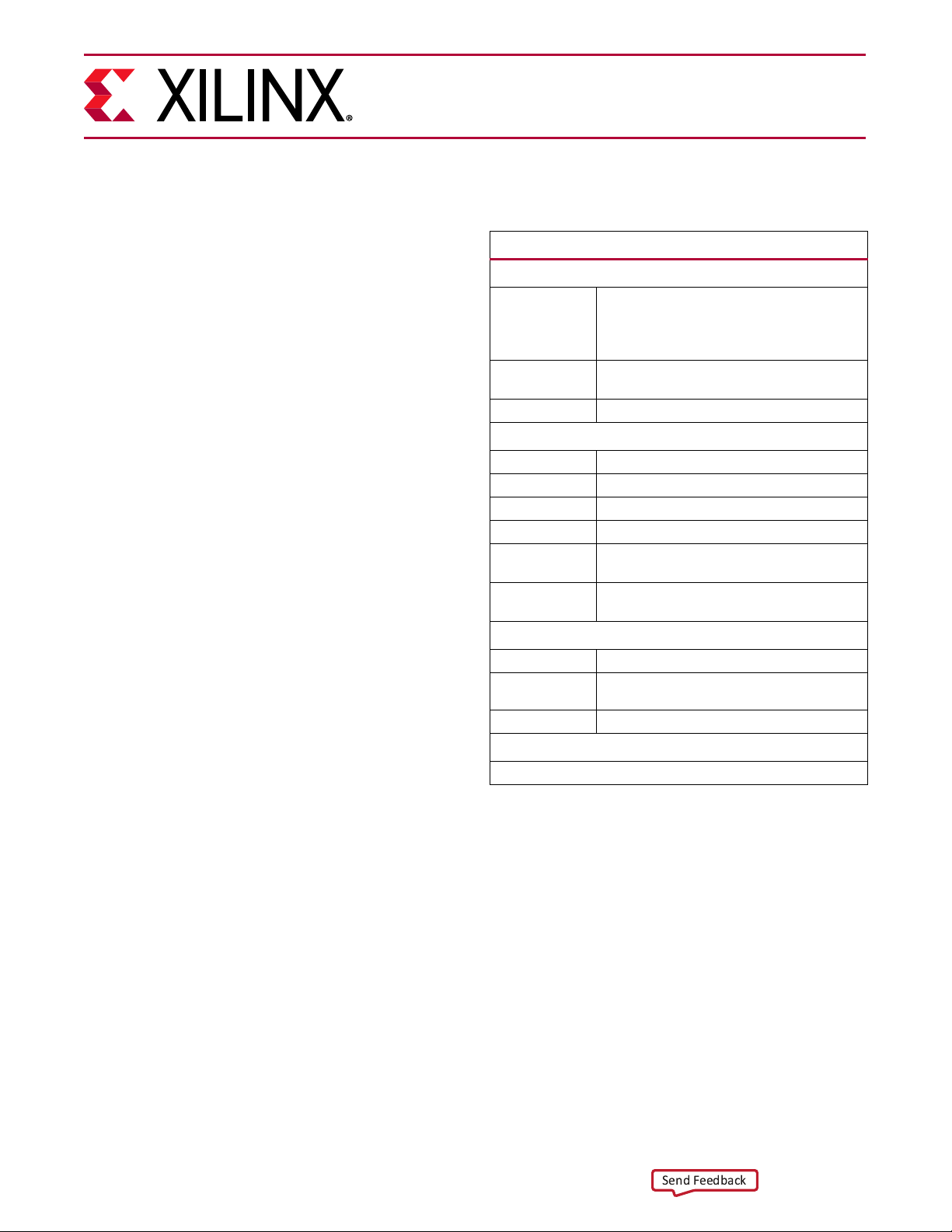
IP Facts Table
Subsystem Specifics
UltraScale+™,
Supported
Device Family
Supported User
Interfaces
Resources Performance and Resource Utilization web page
(1)
Zynq® UltraScale+ MPSoC,
Zynq®-7000 SoC,
7 Series FPGAs
AXI4-Lite, AXI4-Stream
Provided with Subsystem
Design Files Encrypted RTL
Example Design Vivado IP Integrator
Test Bench Not Provided
Constraints File XDC
Simulation
Model
Supported
S/W Driver
(2)
Tested Design Flows
Design Entry Vivado® Design Suite
Simulation
Synthesis Vivado Synthesis
For supported simulators, see the
Xilinx Design Tools: Release Notes Guide.
Not Provided
Standalone and Linux
(3)
Support
Provided by Xilinx at the Xilinx Support web page
Notes:
1. For a complete list of supported devices, see the Vivado IP
catalog.
2. Standalone driver details can be found in the SDK directory
(<install_directory>/SDK/<release>/data/embeddedsw/doc/
xilinx_drivers.htm). Linux OS and driver support information
is available from the
Xilinx Wiki page.
3. For the supported versions of the tools, see the
Xilinx Design Tools: Release Notes Guide.
• Interrupt generation to indicate subsystem
status information
• Internal D-PHY allows direct connection to
image sources
MIPI CSI-2 RX Subsystem v4.0 4
PG232 July 02, 2019 www.xilinx.com Product Specification
Page 5
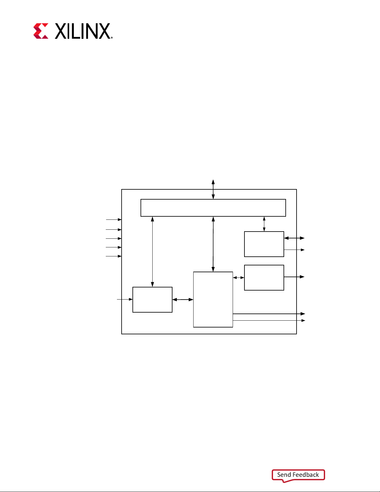
Overview
AXI Crossbar
AXI IIC
Video
Format
Bridge
MIPI CSI-2 RX
Controller
MIPI D-PHY
Video Interface
(AXI4-Stream)
Embedded Non-Image
Interface (AXI4-Stream)
csirxss_csi_irq
csirxss_iic_irq
Serial Interface
AXI4-Lite Interface
IIC Interface
PPI
dphy_clk_200M
lite_aclk
lite_aresetn
video_aclk
video_aresetn
Send Feedback
The MIPI CSI-2 RX subsystem allows you to quickly create systems based on the MIPI
protocol. It interfaces between MIPI-based image sensors and an image sensor pipe. An
internal high speed physical layer design, D-PHY, is provided that allows direct connection
to image sources. The top level customization parameters select the required hardware
blocks needed to build the subsystem. Figure 1-1 shows the subsystem architecture.
X-Ref Target - Figure 1-1
Chapter 1
MIPI CSI-2 RX Subsystem v4.0 5
PG232 July 02, 2019 www.xilinx.com
Figure 1-1: Subsystem Architecture
The subsystem consists of the following sub-cores:
•MIPI D-PHY
• MIPI CSI-2 RX Controller
• AXI CrossbarVideo Format Bridge
•AXI IIC
Page 6

Chapter 1: Overview
Send Feedback
Sub-Core Details
MIPI D-PHY
The MIPI D-PHY IP core implements a D-PHY RX interface and provides PHY protocol layer
support compatible with the CSI-2 RX interface. The MIPI D-PHY IP core also supports the
deskew pattern detection for line rates >1.5 Gb/s. See the MIPI D-PHY LogiCORE IP Product
Guide (PG202) [Ref 3] for details. MIPI D-PHY implementation differs for the UltraScale+
devices and the 7 Series devices with respect to I/O.
For UltraScale+ devices, the Vivado IDE provides a Pin Assignment Tab to select the
required I/O. However, for the 7 series devices the clock capable I/O should be selected
manually. In addition, the 7 series devices do not have a native MIPI IOB support. You will
have to target either HR bank I/O or HP bank I/O for the MIPI IP implementation. For more
information on MIPI IOB compliant solution and guidance, refer D-PHY Solutions (XAPP894)
[Ref 15].
MIPI CSI-2 RX Controller
The MIPI CSI-2 RX Controller core consists of multiple layers defined in the MIPI CSI-2 RX
1.1 specification, such as the lane management layer, low level protocol and byte to pixel
conversion.
The MIPI CSI-2 RX Controller core receives 8-bit data per lane, with support for up to 4
lanes, from the MIPI D-PHY core through the PPI. As shown in Figure 1-1 the byte data
received on the PPI is then processed by the low level protocol module to extract the real
image information. The final extracted image is made available to the user/processor
interface using the AXI4-Stream protocol. The lane management block always operates on
32-bit data received from PPI irrespective number of lanes.
MIPI CSI-2 RX Subsystem v4.0 6
PG232 July 02, 2019 www.xilinx.com
Page 7
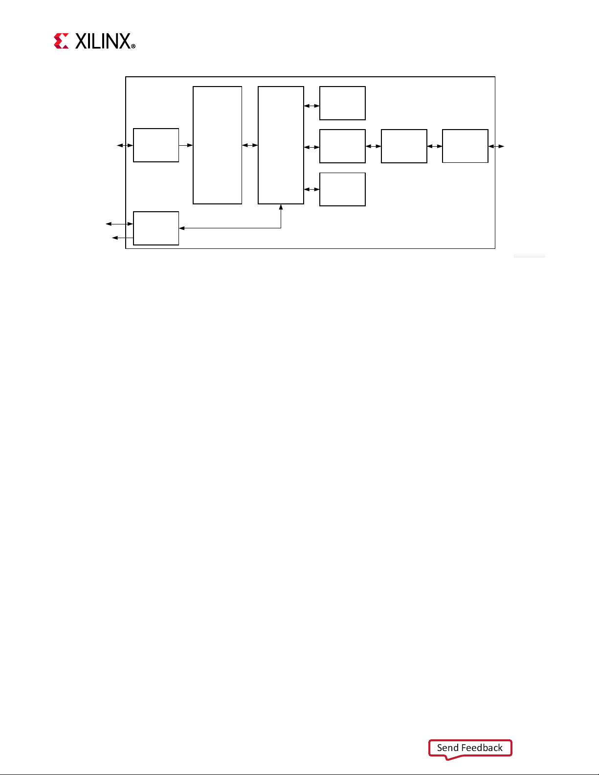
Chapter 1: Overview
PHY Protocol
Interface
(PPI)
Lane
Management
Control
FSM
PHECC
Processing
Data
Processing
CRC
Checker
Buffer
AXI4-
Stream
Register
Interface
AXI4-Stream
PPI
AXI4-Lite
Interrupt
X16317-031116
Send Feedback
X-Ref Target - Figure 1-2
Figure 1-2: MIPI CSI-2 RX Controller Core
Features of this core include:
• 1–4 lane support, with register support to select active lanes (the actual number of
available lanes to be used)
• Short and long packets with all word count values supported
• Primary and many secondary video formats supported
• Data Type (DT) interleaving
• Virtual Channel Identifier (VC) interleaving
• Combination of Data Type and VC interleaving
• Multi-lane interoperability
• Error Correction Code (ECC) for 1-bit error correction and 2-bit error detection in
packet header
• CRC check for payload data
• Long packet ECC/CRC forwarding capability for downstream IPs
• Maximum data rate of 2.5 Gb/s
• Pixel byte packing based on data format
• AXI4-Lite interface to access core registers
• Low power state detection
• Error detection (D-PHY Level Errors, Packet Level Errors, Protocol Decoding Level Errors)
MIPI CSI-2 RX Subsystem v4.0 7
PG232 July 02, 2019 www.xilinx.com
• AXI4-Stream interface with 32/64-bit TDATA width support to offload pixel information
externally
• Interrupt support for indicating internal status/error information
Page 8
Chapter 1: Overview
Send Feedback
As shown in Tab le 1-1 the embedded non-image (with data type code 0x12) AXI4-Stream
interface data width is selected based on the Data Type selected.
Table 1-1: Embedded Non-Image AXI4-Stream Interface TDATA Widths
Data Type (DT) AXI4-Stream Interface TDATA Width
RAW6 32
RAW7 32
RAW8 32
RAW10 64
RAW12 64
RAW14 64
RAW16 64
RAW20 64
All RGB 64
YUV 422 8–bit 64
YUV 422 10–bit 64
Abrupt termination events such as a soft reset, disabling a core while a packet is being
written to the line buffer, or a line buffer full condition results in early termination. The
termination is implemented by assertion of EOL on the video interface or TLAST and
TUSER[1] on the embedded non-image interface, based on the current long packet being
processed.
ECC/CRC Forwarding
Sideband signals of AXI4-Stream interface [Include/Exclude Video Format Bridge and
Embedded non-image interface] report E CC an d CRC data receive d from th e source [s e nsor]
to downstream IPs. This allows to re-calculate ECC/CRC by the downstream IPs in certain
functional safety applications. See Port Descriptions for details on signal mapping.
In error scenarios like abrupt termination due to soft reset, disabling the core while packet
transfer in progress, line buffer in full condition, word count of received packet is greater
than the actual payload, these sideband signals do not report the correct ECC and CRC.
VCX Support
The MIPI CSI-2 standard v2.0 specific VCX support feature is used to extend the maximum
number of available virtual channels to 16. When this feature is enabled, the virtual channel
is deduced by combining the 2-bit VC field (LSB) and the 2-bit VCX field (MSB) from the
packet header.
MIPI CSI-2 RX Subsystem v4.0 8
PG232 July 02, 2019 www.xilinx.com
Page 9

Chapter 1: Overview
Send Feedback
AXI Crossbar
The AXI Crossbar core is used in the subsystem to route AXI4-Lite requests to
corresponding sub-cores based on the address. See the AXI Interconnect LogiCORE IP
Product Guide [Ref 4] for details.
Video Format Bridge
The Video Format Bridge core uses the user-selected VC and Data Type information to filter
onl y the re quired AXI4- Stre am dat a beats . This AXI4-Strea m data is further processed based
on the Data Type information and the output is based on the requested number of pixels
per beat. The output interface adheres to the protocol defined in the AXI4-Stream Video IP
and System Design Guide (UG934) [Ref 2].
The Video Format Bridge core processes the data type selected in the Vivado Integrated
Design Environment (IDE) and filters out all other data types except for RAW8 and User
Defined Byte-based Data types (0x30 to 0x37) received from the CSI-2 RX Controller.
Irrespective of the Vivado IDE selection, RAW8 and User Defined Byte-based Data types are
always processed by the Video Format Bridge core. This allows multiple data-type support,
one main data-type from the Vivado IDE for pixel data and a User Defined Byte-based Data
type for metadata. When multiple data types are transferred (for example, RAW10 and User
Defined Byte-based Data) the actual placement pixel data bits are defined in the
AXI4-Stream Video IP and System Design Guide (UG934) [Ref 2].
For unaligned transfers there is no way to specify the partial final output (TKEEP) for the
output interface. Ensure that you take this into consideration and discard the unintended
bytes in the last beats when there are un-aligned transfers.
video_out Port Width
The width of the data port in the video_out interface depends on the data type selected
and number of pixels per beat selected. The width is a maximum of the RAW8 and the data
type selected in the Vivado IDE multiplied by number of pixels per beat. This is then
rounded to the nearest byte boundary as per the AXI4-Stream protocol.
Example 1: RAW10 and Two Pixels per Clock Selected in the Vivado IDE
• Single pixel width of RAW10 =10
• Single pixel width of RAW8 = 8
For the selected two pixels per clock, the effective pixels widths are 20 and 16 for RAW10
and RAW8 respectively. The video_out port width is configured as the maximum of the
individual pixel widths, and rounded to the nearest byte boundary. This results in a
video_out port width of 24.
MIPI CSI-2 RX Subsystem v4.0 9
PG232 July 02, 2019 www.xilinx.com
Page 10

Chapter 1: Overview
Send Feedback
Example 2: RAW7 and Four Pixels per Clock Selected in the Vivado IDE
• Single pixel width of RAW7 = 7
• Single pixel width of RAW8 = 8
With four pixels per clock selected, the effective pixels widths are 28 and 32 for RAW7 and
RAW8 respectively. The video_out port width is configured as the maximum of the
individual pixel widths, and rounded to nearest byte boundary. This results in a video_out
port width of 32.
Pixel Packing for Multiple Data Types
When multiple pixels are transferred with different pixel width, the pixels with lower width
are justified to most significant bits.
Example 1
When RAW12 and RAW8 are transferred with two pixels per clock, the data port width of the
video_out interface is 24-bits. Within the 24-bits the RAW8 pixels are aligned to the most
significant bits as shown in the following table:
IMPORTANT: In a multi pixel scenario pixel width varies, pixels with lower width are justified to the
most significant bit.
Table 1-2: Pixel Packing for RAW12 and RAW8 Data Types
Bit Positions23222120191817161514131211109876543210
RAW12
RAW8
Notes:
1. p0 to p11 is the 1st pixel bits of RAW12; q0 to q11 is the 2nd pixel bits of RAW12.
2. p0 to p7 is the 1st pixel bits of RAW8; q0 to q7 is the 2nd pixel bits of RAW8.
q11 q10 q9 q8 q7 q6 q5 q4 q3 q2 q1 q0 p11 p10 p9 p8 p7 p6 p5 p4 p3 p2 p1 p0
q7 q6 q5 q4 q3 q2 q1 q0 p7 p6 p5 p4 p3 p2 p1 p0
Example 2
When the core is configured with RAW6 and two pixels per clock, the video_out port
width is set to 16-bits. Within the 16-bits the RAW6 and RAW8 pixels are aligned to the
most significant bits as shown in the following table:
MIPI CSI-2 RX Subsystem v4.0 10
PG232 July 02, 2019 www.xilinx.com
Page 11
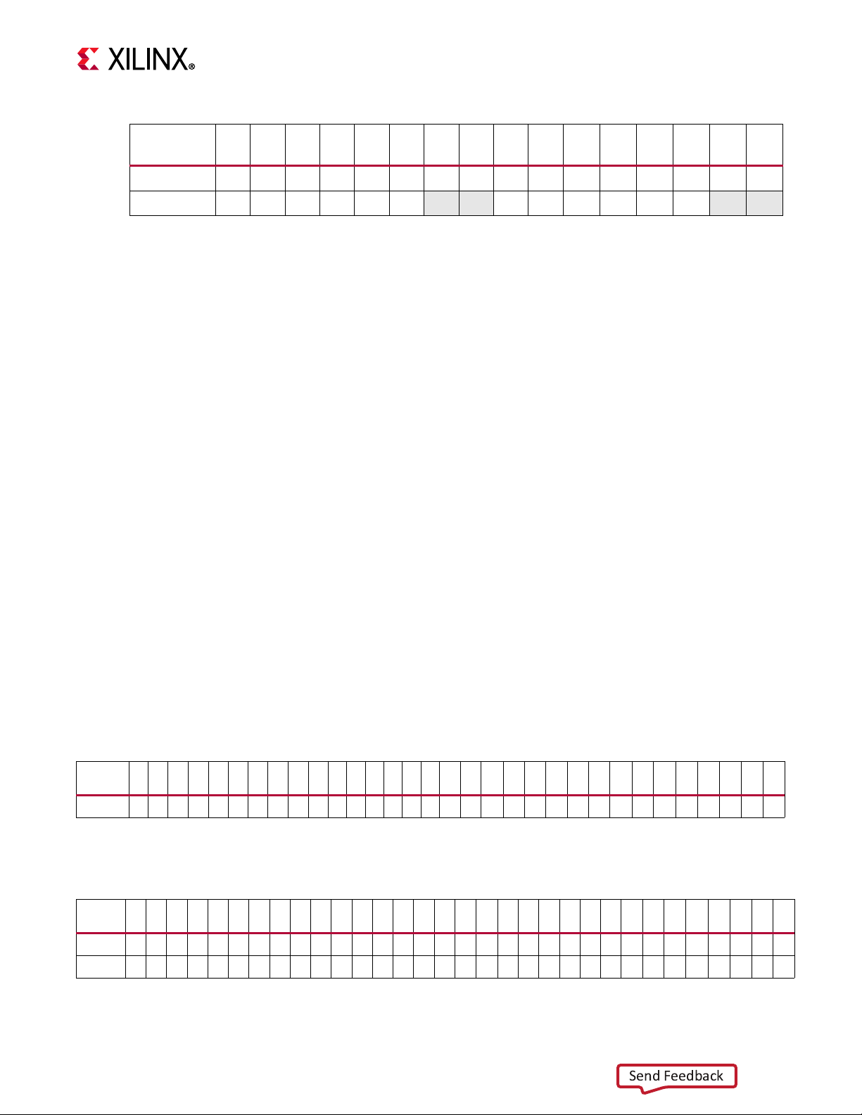
Table 1-3: Pixel Packing for RAW8 and RAW6 Data Types
Send Feedback
Chapter 1: Overview
Bit
Positions
RAW8
RAW6
Notes:
1. p0 to p7 is the 1st pixel bits of RAW8; q0 to q7 is the 2nd pixel bits of RAW8.
2. p0 to p5 is the 1st pixel bits of RAW6; q0 to q5 is the 2nd pixel bits of RAW6.
15141312111098765 4 3 2 1 0
q7 q6 q5 q4 q3 q2 q1 q0 p7 p6 p5 p4 p3 p2 p1 p0
q5 q4
q3 q2 q1 q0
p5 p4 p3 p2 p1 p0
Pixel Packing for Embedded Non-Image Data Types
AXI4-Stream TDATA width is based on main data type selected from the Vivado® IDE. The
position of embedded non-image data type bytes on emb_nonimg_tdata are listed
below:
• 1st byte on emb_nonimg_tdata[7:0]
•2nd byte on emb_nonimg_tdata[15:8] and so on.
Pixel Packing When Video Format Bridge is Not Present
The width of the data port in the video_out can be selected from Vivado IDE, under CSI-2
Options TDATA width. MI P I CSI-2 RX Subsyste m follows t he Recommended Memory Storage
section of the MIPI CSI-2 specifications to output pixels, when a video format bridge is not
present.
For more information the data type packing, refer MIPI Alliance Standard for Camera Serial
Interface CSI-2 Specification [Ref 1].
Example
Pixel mapping for different data types are shown in the following table:
Table 1-4: Pixel Packing for RAW8 Data Type
Bit
Position
RAW8
Notes:
1. p0 to p7 is the 1st pixel bits of RAW8; q0 to q7 is the 2nd pixel bits of RAW8.
Table 1-5: Pixel Packing for RAW10 Data Type
Position
RAW10
RAW10
31 30 29 28 27 26 25 24 23 22 21 20 19 18 17 16 15 14 13 12 11 10 9 8 7 6 5 4 3 2 1 0
s7 s6 s5 s4 s3 s2 s1 s0 r7 r6 r5 r4 r3 r2 r1 r0 q7 q6 q5 q4 q3 q2 q1 q0 p7 p6 p5 p4 p3 p2 p1 p0
Bit
31 30 29 28 27 26 25 24 23 22 21 20 19 18 17 16 15 14 13 12 11 10 9 8 7 6 5 4 3 2 1 0
s9 s8 s7 s6 s5 s4 s3 s2 r9 r8 r7 r6 r5 r4 r3 r2 q9 q8 q7 q6 q5 q4 q3 q2 p9 p8 p7 p6 p5 p4 p3 p2
v9 v8 v7 v6 v5 v4 v3 v2 u9 u8 u7 u6 u5 u4 u3 u2 t9 t8 t7 t6 t5 t4 t3 t2 s1 s0 r1 r0 q1 q0 p1 p0
MIPI CSI-2 RX Subsystem v4.0 11
PG232 July 02, 2019 www.xilinx.com
Page 12

Chapter 1: Overview
Send Feedback
Table 1-5: Pixel Packing for RAW10 Data Type
Bit
Position
RAW10
Notes:
1. In RAW10, MSB 8-bits of 4 pixels are transferred first, followed by LSB 2-bits of each pixel.
31 30 29 28 27 26 25 24 23 22 21 20 19 18 17 16 15 14 13 12 11 10 9 8 7 6 5 4 3 2 1 0
y9 y8 y7 y6 y5 y4 y3 y2 x9 x8 x7 x6 x5 x4 x3 x2 w1 w0 v1 v0 u1 u0 t1 t0 w9 w8 w7 w6 w5 w4 w3 w2
Table 1-6: Pixel Packing for RGB888 Data Type
Bit
Position
RGB888
RGB888
Notes:
1. In RGB888, a0 to a7 represents the B component, b0 to b7 represents the G component and c0 to c7 represents the R
313029282726252423222120191817161514131211109876543210
d7 d6 d5 d4 d3 d2 d1 d0 c7 c6 c5 c4 c3 c2 c1 c0 b7 b6 b5 b4 b3 b2 b1 b0 a7 a6 a5 a4 a3 a2 a1 a0
h7 h6 h5 h4 h3 h2 h1 h0 g7 g6 g5 g4 g3 g2 g1 g0 f7 f6 f5 f4 f3 f2 f1 f0 e7 e6 e5 e4 e3 e2 e1 e0
component.
AXI IIC
The Camera Control Interface (CCI) of the MIPI CSI-2 specification is compatible with the
fast mode variant of the I2C interface with 400 kHz operation and 7-bit slave addressing.
The AXI IIC is made available as part of this subsystem depending on user selections. See
the AXI IIC Bus Interface v2.0 LogiCORE IP Product Guide (PG090) [Ref 5] for details.
Applications
The Xilinx MIPI CSI-2 RX controller implements a Camera Serial Interface between a camera
sensor and a programmable device performing baseband processing. Bandwidth
requirement for the camera sensor interface has gone up due to the development of higher
resolution cameras. Traditional parallel interfaces require an increasing number of signal
lines resulting in higher power consumption. The new high speed serial interfaces, such as
MIPI CSI specifications, address these expanding bandwidth requirements without
sacrificing power. MIPI is a group of protocols defined by the mobile industry group to
standardize all interfaces within mobile platforms such as mobile phones and tablets.
However the large volumes and the economies of scale of the mobile industry is forcing
other applications to also adopt these standards. As such MIPI-based camera sensors are
being increasingly used in applications such as driver assistance technologies in automotive
applications, video security surveillance cameras, video conferencing and emerging
applications such as virtual and augmented reality.
MIPI CSI-2 RX Subsystem v4.0 12
PG232 July 02, 2019 www.xilinx.com
Page 13

Chapter 1: Overview
Send Feedback
Unsupported Features
• Some YUV Data Types (YUV 420 (8-bit and 10-bit)) are not supported when the Video
Format Bridge is included.
• Dynamic linerate is not supported.
• 8 lanes support is not included.
• Data scramble feature is not supported.
• Latency reduction and transport efficiency features are not supported.
Licensing and Ordering
License Checkers
If the IP requires a license key, the key must be verified. The Vivado® design tools have
several license checkpoints for gating licensed IP through the flow. If the license check
succeeds, the IP can continue generation. Otherwise, generation halts with error. License
checkpoints are enforced by the following tools:
• Vivado synthesis
• Vivado implementation
• write_bitstream (Tcl command)
IMPORTANT: IP license level is ignored at checkpoints. The test confirms a valid license exists. It does
not check IP license level.
License Type
This Xilinx module is provided under the terms of the Xilinx Core License Agreement. The
module is shipped as part of the Vivado® Design Suite. For full access to all core
functionalities in simulation and in hardware, you must purchase a license for the core.
Contact your local Xilinx sales representative for information about pricing and availability.
For more information, visit the MIPI CSI-2 RX Subsystem product web page.
MIPI CSI-2 RX Subsystem v4.0 13
PG232 July 02, 2019 www.xilinx.com
Information about other Xilinx LogiCORE IP modules is available at the Xilinx Intellectual
Property page. For information on pricing and availability of other Xilinx LogiCORE IP
modules and tools, contact your local Xilinx sales representative.
Page 14

Product Specification
Send Feedback
Standards
• MIPI Alliance Standard for Camera Serial Interface CSI-2 v1.1 [Ref 1]
•MIPI Alliance Physical Layer Specifications, D-PHY Specification v1.1 [Ref 6]
• Processor Interface, AXI4-Lite: see the Vivado Design Suite: AXI Reference Guide
(UG1037) [Ref 7]
• Output Pixel Interface: see the AXI4-Stream Video IP and System Design Guide (UG934)
[Ref 2]
Chapter 2
Performance
This section details the performance information for various core configurations.
Latency
The CSI2 RX Subsystem core latency is the time from the start-of-transmission (SoT) pattern
on the serial lines to the tvalid signal assertion at CSI-2 Rx Subsystem output. This includes
the D-PHY latency, MIPI RX Controller latency and VFB latency (if Video Format Bridge is
included in the Subsystem).
Figure 2-1 represents the latency calculation for the subsystem
MIPI CSI-2 RX Subsystem v4.0 14
PG232 July 02, 2019 www.xilinx.com
Page 15

X-Ref Target - Figure 2-1
1-4-'76<79&7=78)1
(4,= :*&
V\F]XIGPO(SQEMR
:MHIS'PSGO(SQEMR
7IVMEP0MRIW
(4,=0EXIRG]
'SRXVSPPIV0EXIRG]
:*&0EXIRG]
44-
7XVIEQMRK-*
7XVIEQMRK-*
1-4-'7-6<
'SRXVSPPIV
<
Send Feedback
Chapter 2: Product Specification
D-PHY latency:
The MIPI D-PHY RX core latency is the time from the start-of-transmission (SoT) pattern on
the serial lines to the activehs signal assertion on the PPI .The HS_SETTLE period contributes
significantly in the D-PHY latency calculation.
Tab le 2-1 provides the latency numbers for various core configurations.
Table 2-1: D-PHY Latency
Data Type Pixel Mode Line Rate
RAW20 Single
RAW8 Single
RAW8 Dual
RAW8 Quad
RAW10 Single
Figure 2-1: MIPI CSI2 RX Subsystem Latency Calculation
Latency in
rxbyteclk
(HS_SETTLE +
internal latency)
1000 26(23+3)
1000 26(23+3)
1000 26(23+3)
1000 26(23+3)
1000 26(23+3)
MIPI CSI-2 RX Subsystem v4.0 15
PG232 July 02, 2019 www.xilinx.com
RAW10 Dual
RAW10 Quad
Notes: All the calculations are made for a single lane design with a fixed
video clock of 148 MHz.
1200 30(26+4)
800 22(20+2)
Page 16
Chapter 2: Product Specification
Send Feedback
MIPI CSI-2 RX Controller latency:
The MIPI CSI-2 RX Controller core latency is the time from the activehs assertion on the PPI
Interface to valid signal assertion on the controller output.
Tab le 2-2 provides the latency numbers for various core configurations.
Table 2-2: MIPI CSI2 RX Controller latency
Data Type Pixel Mode Line Rate
RAW20 Single
RAW8 Single
RAW8 Dual
RAW8 Quad
RAW10 Single
RAW10 Dual
RAW10 Quad
Notes: All the calculations are made for a single lane design with a fixed video clock of 148
MHz.
1000 25 60
1000 21 49
1000 21 49
1000 21 49
1000 25 60
1200 26 63
800 24 56
Latency in
rxbyteclk
Latency in Video
Clock
Video Format Bridge (VFB) latency:
The VFB core latency is the time time from the VFB input stream interface ‘tvalid’ to VFB
output stream interface ‘tvalid’.
Tab le 2-3 provides the latency numbers for various core configurations.
Table 2-3: VFB latency
MIPI CSI-2 RX Subsystem v4.0 16
PG232 July 02, 2019 www.xilinx.com
Data Type Pixel Mode Line Rate
RAW20 Single
RAW8 Single
RAW8 Dual
RAW8 Quad
RAW10 Single
RAW10 Dual
RAW10 Quad
Notes: All the calculations are made for a fixed video clock of 148 MHz.
1000 10 24
1000 1 3
1000 1 3
1000 1 4
1000 2 6
1200 3 6
800 1 3
Latency in
rxbyteclk
Latency in Video
Clock
Page 17
Chapter 2: Product Specification
Send Feedback
Tab le 2-4 provides the overall latency numbers of MIPI CSI2 RX Subsystem for various core
configurations.
Table 2-4: MIPI CSI2 RX Subsystem Latency
Data Type Pixel Mode Line Rate
RAW20 Single
RAW8 Single
RAW8 Dual
RAW8 Quad
RAW10 Single
RAW10 Dual
RAW10 Quad
Notes:
1. All the calculations are made for a single lane design with a fixed video
clock of 148 MHz.
2. The latency is improved by increasing the number of lanes.
1000 61
1000 48
1000 48
1000 48
1000 53
1200 59
800 47
Latency in
rxbyteclk
Resource Utilization
For full details about performance and resource utilization, visit the Performance and
Resource Utilization web page.
MIPI CSI-2 RX Subsystem v4.0 17
PG232 July 02, 2019 www.xilinx.com
Port Descriptions
The MIPI CSI-2 RX Subsystem I/O signals are described in Ta ble 2 - 5.
Table 2-5: Port Descriptions
Signal Name Direction Description
lite_aclk Input AXI clock
lite_aresetn Input AXI reset. Active-Low
S00_AXI*
dphy_clk_200M Input Clock for D-PHY core. Must be 200 MHz.
video_aclk Input Subsystem clock
video_aresetn
(1)
Input Subsystem reset. Active-Low.
AXI4-Stream Video Interface when Video Format Bridge is Present
video_out_tvalid Output Data valid
AXI4-Lite interface, defined in the Vivado Design Suite: AXI
Reference Guide (UG1037) [Ref 7]
Page 18

Table 2-5: Port Descriptions (Cont’d)
Send Feedback
Signal Name Direction Description
video_out_tready Input Slave ready to accept the data
n is based on TUSER width selected in the Vivado IDE
95-80 CRC
79-72 ECC
71-70 Reserved
69-64 Data Type
(3)
Chapter 2: Product Specification
video_out_tuser[n-1:0] Output
video_out_tlast Output End of line
video_out_tdata[n-1:0] Output
video_out_tdest[9:0] Output
63-48 Word Count
47-32 Line Number
31-16 Frame Number
15-2 Reserved
1 Packet Error
0Start of Frame
Data
n is based on Data type and number of pixels selected in the
Vivado IDE (see video_out Port Width).
9-4 Data Type
3-0 Virtual Channel Identifier (VC)
(2)
AXI4-Stream Interface when Embedded Non-image Interface is Selected
Data
emb_nonimg_tdata[n-1:0] output
emb_nonimg_tdest[3:0] Output
n is based on Data type selected in the Vivado IDE (see
Tabl e 1- 1).
Specifies the Virtual Channel Identifier (VC) value of the
embedded non-image packet
MIPI CSI-2 RX Subsystem v4.0 18
PG232 July 02, 2019 www.xilinx.com
emb_nonimg_tkeep[n/8-1:0] Output Specifies valid bytes
emb_nonimg_tlast Output End of line
emb_nonimg_tready Input Slave ready to accept data
Page 19

Table 2-5: Port Descriptions (Cont’d)
Send Feedback
Signal Name Direction Description
95-80 CRC
79-72 ECC
71-70 Reserved
69-64 Data Type
(3)
Chapter 2: Product Specification
emb_nonimg_tuser[95:0] Output
emb_nonimg_tvalid Output Data valid
63-48 Word Count
47-32 Line Number
31-16 Frame Number
15-2 Reserved
1 Packet Error
0 Start of frame
AXI4-Stream Interface when Video Format Bridge is Not Present
video_out_tdata[n-1:0] Output
video_out_tdest[n-1:0] Output
video_out_tkeep[n/8-1:0] Output Specifies valid bytes
video_out_tlast Output End of line
video_out_tready Input Slave ready to accept data
Data
n is based on TDATA width selected in the Vivado IDE.
n is based on TDEST width selected in the Vivado IDE:
9-4 Data type
3-0 Virtual Channel Identifier (VC)
n is based on TUSER width selected in the Vivado IDE
95-80 CRC
(3)
(2)
MIPI CSI-2 RX Subsystem v4.0 19
PG232 July 02, 2019 www.xilinx.com
79-72 ECC
71-70 Reserved
69-64 Data Type
video_out_tuser[n-1:0] Output
video_out_tvalid Output Data valid
63-48 Word Count
47-32 Line Number
31-16 Frame Number
15-2 Reserved
1 Packet Error
0 Start of frame
(2)
Other Signals
csirxss_csi_irq Output Interrupt (active-High) from CSI-2 RX Controller
csirxss_iic_irq Output Interrupt (active-High) from AXI IIC
Page 20

Chapter 2: Product Specification
Send Feedback
Table 2-5: Port Descriptions (Cont’d)
Signal Name Direction Description
Xilinx 7 series FPGA
mipi_dphy_if Output DPHY interface
rxbyteclkhs Output PPI high-speed receive byte clock
system_rst_out Output Reset indication due to PLL reset (active-High)
dlyctrl_rdy_out Output
clk_300m Input 300 MHz clock for IDELAYCTRL
Ready signal output from IDEALYCTRL, stating delay values
are adjusted as per vtc changes
UltraScale+ Shared Logic outside Subsystem
mipi_phy_if Output DPHY interface
rxbyteclkhs Output PPI high-speed receive byte clock
clkoutphy_out Output PHY serial clock
system_rst_out Output Reset indication due to PLL reset (active-High)
pll_lock_out Output PLL lock indication (active-High)
UltraScale+ Shared logic in the Subsystem
mipi_phy_if Output DPHY interface
Inferred bitslice ports. The core infers bitslice0 of a nibble for
strobe propagation within the byte group; <x> indicates byte
group (0,1,2,3); <y> indicates bitslice0 position (0 for the
lower nibble, 6 for the upper nibble)
bg<x>_pin<y>_nc Input
• RTL Design: There is no need to drive any data on these
ports.
• IP Integrator: These ports must be brought to the top level
of the design to properly apply the constraints.
Note:
Pins are available only for UltraScale+ families.
MIPI CSI-2 RX Subsystem v4.0 20
PG232 July 02, 2019 www.xilinx.com
clkoutphy_in Input PHY serial clock
pll_lock_in Input PLL Lock indication
rxbyteclkhs Output PPI high-speed receive byte clock
Notes:
1. The active-High reset for the MIPI D-PHY core is generated internally by setting the external
active-Low reset (video_aresetn) to 0.
2. Each frame start packet with Virtual Channel (VC) identifier will be mapped to the first image packet and the first
embedded non-image with the corresponding VC.
3. As CRC appears at the end of the MIPI packet, ECC and CRC are reported ONLY during the last beat of the stream
transfer when TLAST and TVALID are asserted. You need to ignore ECC/CRC reported during other beats of the
transfer. See Interface Debug for more details.
Page 21

Chapter 2: Product Specification
Send Feedback
Register Space
This section details registers available in the MIPI CSI-2 RX Subsystem. The address map is
split into following regions:
• MIPI CSI-2 RX Controller core
•AXI IIC core
•MIPI D-PHY core
Each IP core is given an address space of 64K. Example offset addresses from the system
base address when the AXI IIC and MIPI D-PHY registers are enabled are shown in Tabl e 2-6.
Table 2-6: Sub-Core Address Offsets
IP Cores Offset
MIPI CSI-2 RX Controller 0x0_0000
AXI IIC 0x1_0000
MIPI D-PHY 0x2_0000
(1)
Notes:
1. When the AXI IIC core is not present, the MIPI D-PHY offset moves up and starts at 0x1_0000. The software driver
handles this seamlessly.
MIPI CSI-2 RX Controller Core Registers
Tab le 2-7 specifies the name, address, and description of each firmware addressable
register within the MIPI CSI-2 RX controller core.
Table 2-7: MIPI CSI-2 RX Controller Core Registers
Address Offset Register Name Description
0x00 Core Configuration Register Core configuration options
0x04
0x08 Reserved
0x0C Reserved
0x10 Core Status Register Internal status of the core
0x14 Reserved
0x18 Reserved
0x1C Reserved
Protocol Configuration
Register
(1)
Protocol configuration options
MIPI CSI-2 RX Subsystem v4.0 21
PG232 July 02, 2019 www.xilinx.com
0x20
0x24 Interrupt Status Register Interrupt status register
Global Interrupt Enable
Register
Global interrupt enable registers
Page 22

Chapter 2: Product Specification
Send Feedback
Table 2-7: MIPI CSI-2 RX Controller Core Registers (Cont’d)
Address Offset Register Name Description
0x28 Interrupt Enable Register Interrupt enable register
0x2C Reserved
0x30 Generic Short Packet Register Short packet data
0x34 VCX Frame Error Register VCX Frame Error Register
0x38 Reserved
0x3C
Lane<n> Information Registers
0x40 Lane0 Information Lane 0 status information
0x44 Lane1 Information Lane 1 status information
0x48 Lane2 Information Lane 2 status information
0x4C Lane3 Information Lane 3 status information
0x50 Reserved
0x54 Reserved
0x58 Reserved
0x5C Reserved
Image Information 1 Registers (VC0 to VC15) and Image Information 2 Registers (VC0 to VC15)
0x60 Image Information 1 for VC0
0x64 Image Information 2 for VC0
0x68 Image Information 1 for VC1
Clock Lane Information
Register
Clock lane status information
Image information 1 of the current processing packet
with VC of 0
Image information 2 of the current processing packet
with VC of 0
Image information 1 of the current processing packet
with VC of 1
MIPI CSI-2 RX Subsystem v4.0 22
PG232 July 02, 2019 www.xilinx.com
0x6C Image Information 2 for VC1
0x70 Image Information 1 for VC2
0x74 Image Information 2 for VC2
0x78 Image Information 1 for VC3
0x7C Image Information 2 for VC3
0x80 Image Information 1 for VC4
0x84 Image Information 2 for VC4
0x88 Image Information 1 for VC5
Image information 2 of the current processing packet
with VC of 1
Image information 1 of the current processing packet
with VC of 2
Image information 2 of the current processing packet
with VC of 2
Image information 1 of the current processing packet
with VC of 3
Image information 2 of the current processing packet
with VC of 3
Image information 1 of the current processing packet
with VC of 4
Image information 2 of the current processing packet
with VC of 4
Image information 1 of the current processing packet
with VC of 5
Page 23

Chapter 2: Product Specification
Send Feedback
Table 2-7: MIPI CSI-2 RX Controller Core Registers (Cont’d)
Address Offset Register Name Description
0x8C Image Information 2 for VC5
0x90 Image Information 1 for VC6
0x94 Image Information 2 for VC6
0x98 Image Information 1 for VC7
0x9C Image Information 2 for VC7
0xA0 Image Information 1 for VC8
0xA4 Image Information 2 for VC8
0xA8 Image Information 1 for VC9
0xAC Image Information 2 for VC9
0xB0
0xB4
Image Information 1 for
VC10
Image Information 2 for
VC10
Image information 2 of the current processing packet
with VC of 5
Image information 1 of the current processing packet
with VC of 6
Image information 2 of the current processing packet
with VC of 6
Image information 1 of the current processing packet
with VC of 7
Image information 2 of the current processing packet
with VC of 7
Image information 1 of the current processing packet
with VC of 8
Image information 2 of the current processing packet
with VC of 8
Image information 1 of the current processing packet
with VC of 9
Image information 2 of the current processing packet
with VC of 9
Image information 1 of the current processing packet
with VC of 10
Image information 2 of the current processing packet
with VC of 10
0xB8
0xBC
0xC0
0xC4
0xC8
0xCC
0xD0
0xD4
0xD8
Image Information 1 for
VC11
Image Information 2 for
VC11
Image Information 1 for
VC12
Image Information 2 for
VC12
Image Information 1 for
VC13
Image Information 2 for
VC13
Image Information 1 for
VC14
Image Information 2 for
VC14
Image Information 1 for
VC15
Image information 1 of the current processing packet
with VC of 11
Image information 2 of the current processing packet
with VC of 11
Image information 1 of the current processing packet
with VC of 12
Image information 2 of the current processing packet
with VC of 12
Image information 1 of the current processing packet
with VC of 13
Image information 2 of the current processing packet
with VC of 13
Image information 1 of the current processing packet
with VC of 14
Image information 2 of the current processing packet
with VC of 14
Image information 1 of the current processing packet
with VC of 15
MIPI CSI-2 RX Subsystem v4.0 23
PG232 July 02, 2019 www.xilinx.com
Page 24

Chapter 2: Product Specification
Send Feedback
Table 2-7: MIPI CSI-2 RX Controller Core Registers (Cont’d)
Address Offset Register Name Description
0xDC
Notes:
1. Access type and reset value for all the reserved bits in the registers is read-only with value 0.
2. Register accesses should be word aligned and there is no support for a write strobe. WSTRB is not used internally.
3. Only the lower 7-bits (6:0) of the read and write address of the AXI4-Lite interface are decoded. This means that
accessing address 0x00 and 0x80 results in reading the same address of 0x00.
4. Reads and writes to addresses outside this table do not return an error.
Image Information 2 for
VC15
Image information 2 of the current processing packet
with VC of 15
Core Configuration Register
The Core Configuration register is described in Ta ble 2 -8 and allows you to enable and
disable the MIPI CSI-2 RX Controller core and apply a soft reset during core operation.
Table 2-8: Core Configuration Register (0x00)
Bits Name Reset Value Access Description
31–2 Reserved N/A N/A Reserved
1: Resets the core
0: Takes core out of soft reset
All registers reset to their default value (except for this
bit, Core Enable and Active lanes configuration).
In addition to resetting registers when this bit is set to 1:
1 Soft Reset 0x0 R/W
• Shut down port is not asserted on the PPI lanes
• Internal FIFOs (PPI, Packet, Generic Short Packet) are
flushed
• Control Finite State Machine (FSM) stops processing
current packet. Any partially written packet to
memory is marked as errored. This packet, when
made available through the AXI4-Stream interface,
reports the error on TUSER[1].
MIPI CSI-2 RX Subsystem v4.0 24
PG232 July 02, 2019 www.xilinx.com
1: Enables the core to receive and process packets
0: Disables the core for operation
When disabled:
• Shuts down port assertion on the PPI lanes
0Core Enable0x1 R/W
Notes:
1. The short packet and line buffer FIFO full conditions take a few clocks to reflect in the register clock domain from
the core clock domain due to Clock Domain Crossing (CDC) blocks.
• Internal FIFOs (PPI, Packet, Generic Short Packet) are
flushed
• Control FSM stops processing current packet
Any partially written packet to memory is marked as
errored. This packet, when made available through
the AXI4-Stream interface, reports the error on
TUSER[1].
Page 25

Chapter 2: Product Specification
Send Feedback
Protocol Configuration Register
The Protocol Configuration register is described in Ta ble 2 -9 and allows you to configure
protocol specific options such as the number of lanes to be used.
Table 2-9: Protocol Configuration Register (0x04)
Bits Name Reset Value Access Description
31–5 Reserved N/A N/A Reserved
Maximum lanes of the core
Number of lanes configured
4–3 Maximum Lanes
2 Reserved N/A Reserved
1–0 Active Lanes
(1)
during core generation
Number of lanes configured
during core generation
R
(2)
/W
R
0x0—1 Lane
0x1—2 Lanes
0x2—3 Lanes
0x3—4 Lanes
Active lanes in the core
0x0—1 Lane
0x1—2 Lanes
0x2 —3 Lanes
0x3—4 Lanes
(3)
Notes:
1. M ax im um La ne s can no t exceed the number of lanes as set by the Serial Data Lanes parameter at generation time.
2. A read from this register reflects the current number of lanes being used by core. This is useful when dynamically
updating the active lanes during core operation to ensure that the core is using the new active lanes information.
See Chapter 3, Designing with the Subsystem for more information.
3. Active Lanes cannot exceed the Maximum Lanes as set in the Protocol Configuration register setting of bits 4–3.
Core Status Register
The Core Status register is described in Tabl e 2-10 .
Table 2-10: Core Status Register (0x10)
Bits Name Reset Value Access Description
Counts number of long packets written to
the line buffer
31–16 Packet Count 0x0 R
15–4 Reserved N/A N/A N/A
3 Short packet FIFO Full 0x0 R
• No roll-over of this counter reported/
supported
• Count includes error packets (if any)
Indicates the current status of short packet
FIFO full condition
MIPI CSI-2 RX Subsystem v4.0 25
PG232 July 02, 2019 www.xilinx.com
2 Short packet FIFO not empty 0x0 R
FIFO not empty: Indicates the current status
of short packet FIFO not empty condition
Page 26

Chapter 2: Product Specification
Send Feedback
Table 2-10: Core Status Register (0x10) (Cont’d)
Bits Name Reset Value Access Description
1 Stream Line buffer Full 0x0 R
Soft reset/Core disable
0
in progress
0x0 R
Indicates the current status of line buffer
full condition
Set to 1 by the core to indicate that
internal soft reset/core disable activities
are in progress
Global Interrupt Enable Register
The Global Interrupt Enable register is described in Ta bl e 2- 1 1.
Table 2-11: Global Interrupt Enable Register (0x20)
Bits Name Reset Value Access Description
31–1 Reserved N/A N/A Reserved
Master enable for the device interrupt output to
the system
0 Global Interrupt enable 0x0 R/W
1: Enabled—the corresponding Interrupt Enable
register (IER) bits are used to generate interrupts
0: Disabled—Interrupt generation blocked
irrespective of IER bits
Interrupt Status Register
The Interrupt Status register (ISR) is described in Tabl e 2 -12 and captures the error and
status information for the core.
Table 2-12: Interrupt Status Register (0x24)
Bits Name
31 Frame Received 0x0 R/W1C
30 VCX Frame Error RO 0x0
30–23 Reserved N/A N/A N/A
22 Word Count (WC) corruption 0x0 R/W1C
Reset
Value
Access
(1)
Asserted when the Frame End (FE) short
packet is received for the current frame
Asserted when the VCX Frame error is
detected
Asserted when WC field of packet header
corrupted and core receives less bytes than
indicated in WC field. Such a case can occur
only where more than 2-bits of header are
corr upted which E CC algorithm cannot report
and the corruption is such that the ECC
algorithm reports a higher Word Count (WC)
value as part of ECC correction.
In such case core limits processing of the
packet on reduced number of bytes received
through PPI interface.
Description
MIPI CSI-2 RX Subsystem v4.0 26
PG232 July 02, 2019 www.xilinx.com
Page 27

Table 2-12: Interrupt Status Register (0x24) (Cont’d)
Send Feedback
Chapter 2: Product Specification
Bits Name
21 Incorrect lane configuration 0x0 R/W1C
20 Short packet FIFO full 0x0 R/W1C
19 Short packet FIFO not empty 0x0 R/W1C
18 Stream line buffer full 0x0 R/W1C Asserts when the line buffer is full
17 Stop state 0x0 R/W1C
16 Reserved N/A N/A N/A
15 Reserved N/A N/A N/A
14 Reserved N/A N/A N/A
SoT error
13
(ErrSoTHS)
SoT sync error
12
(ErrSotSyncHS)
ECC 2-bit error
11
(ErrEccDouble)
Reset
Access
Value
0x0 R/W1C
0x0 R/W1C
0x0 R/W1C
(1)
Asserted when Active lanes is greater than
Maximum lanes in the protocol configuration
register
Active-High signal asserted when the short
packet FIFO full condition detected
Active-High signal asserted when short
packet FIFO not empty condition detected
Active-High signal indicates that the lane
module is currently in Stop state
Indicates Start-of-Transmission (SoT) error
detected
Indicates SoT synchronization completely
failed
As serte d when an ECC syndrome is compu ted
and two bit errors detected in the received
packet header
(3)
(3)
Description
(2)
(3)
ECC 1-bit error
(Detected and Corrected)
10
(ErrEccCorrected)
CRC error
9
(ErrCrc)
Unsupported Data Type
8
(ErrID)
Frame synchronization
7
error for VC3
(ErrFrameSync)
Frame level error for VC3
6
(ErrFrameData)
Frame synchronization
5
error for VC2
(ErrFrameSync)
Frame level error for VC2
4
(ErrFrameData)
0x0 R/W1C
0x0 R/W1C
0x0 R/W1C
0x0 R/W1C
0x0 R/W1C
0x0 R/W1C
0x0 R/W1C
Asserted when an ECC syndrome was
computed and a single bit error in the packet
header was detected and corrected
Asserted when the computed CRC code is
different from the received CRC code
Asserted when a packet header is decoded
with an unrecognized or not implemented
data ID
Asserted when an FE is not paired with a
Frame Start (FS) on the same virtual channel
Asserted after an FE when the data payload
received between FS and FE contains errors.
The data payload errors are CRC errors.
Ass erted when an FE i s not paire d wit h a FS o n
the same virtual channel
Asserted after an FE when the data payload
received between FS and FE contains errors.
The data payload errors are CRC errors.
(4)
(4)
MIPI CSI-2 RX Subsystem v4.0 27
PG232 July 02, 2019 www.xilinx.com
Page 28

Table 2-12: Interrupt Status Register (0x24) (Cont’d)
Send Feedback
Chapter 2: Product Specification
Bits Name
Frame synchronization
3
error for VC1
(ErrFrameSync)
Frame level error for VC1
2
(ErrFrameData)
Frame synchronization
1
error for VC0
(ErrFrameSync)
Frame level error for VC0
0
(ErrFrameData)
Notes:
1. W1C = Write 1 to clear.
2. In a line buffer full condition, reset the core using the external reset, video_aresetn.
3. Reported through the PPI.
4. An ErrSotSyncHS error also generates this error signal.
5. Short packet and line buffer FIFO full conditions take a few clock periods to reflect in the register clock domain
from the core clock domain due to Clock Domain Crossing (CDC) blocks.
6. All PPI si gnals ca pt ured in the ISR take a f ew clock pe ri ods to refl ec t in the r eg ister cloc k d omain from the PPI clo ck
domain due to CDC blocks.
7. Frame level errors due to ErrSotSyncHS are mapped to the recent VC processed by the ECC block of the core.
8. Set conditions take priority over the reset conditions for the ISR bits.
9. Signal names in brackets are defined in the MIPI Alliance Standard for Camera Serial Interface CSI-2 [Ref 1].
Reset
Access
Value
0x0 R/W1C
0x0 R/W1C
0x0 R/W1C
0x0 R/W1C
(1)
Ass erted when an FE i s not paire d wit h a FS o n
the same virtual channel
Asserted after an FE when the data payload
received between FS and FE contains errors.
The data payload errors are CRC errors.
Asserted when a FE is not paired with a FS on
the same virtual channel
Asserted after an FE when the data payload
received between FS and FE contains errors.
The data payload errors are CRC errors.
Description
(4)
(4)
Tables 2-13 to 2-24 provide detailed information about the bits in Ta ble 2 - 12.
Table 2-13: Incorrect Lane Configuration
Set Condition(s)
Reset Sequence Write 1 to clear this bit.
Priority Set condition takes priority over reset sequence.
Impact
Set by the core when incorrect lane configuration is programmed.
Ex: Maximum available lanes =2 and “Active lanes” configured as 3
This is a core configuration error and the core cannot function as desired. This error
should be corrected before proceeding further.
Table 2-14: Stream Line Buffer Full
Set Condition(s) Set by the core when the line buffer storing pixel data is full.
Reset Sequence Write 1 to clear this bit.
Priority Set condition takes priority over reset sequence.
Core reports this condition on stream interface using an error indication on the
Impact
TUSER[1] port if a partial packet is being written to line buffer. Because PPI does not
allow back pressure, you need to ensure that this condition does not occur.
MIPI CSI-2 RX Subsystem v4.0 28
PG232 July 02, 2019 www.xilinx.com
Page 29

Chapter 2: Product Specification
Send Feedback
Table 2-15: Control Error, Escape Entry Error, Escape Ultra Low Power Mode, Stopstate
Set Condition(s)
Reset Sequence Write 1 to clear this bit.
Priority Set condition takes priority over reset sequence.
Impact Current packet being processed does not have any impact.
Set by the core when the condition for the corresponding signal as defined in the
MIPI CSI-2 specification [Ref 1] is seen, reported through the PPI interface.
Table 2-16: SoT Error
Set Condition(s)
Reset Sequence Write 1 to clear this bit.
Priority Set condition takes priority over reset sequence.
Impact
Set by the core when the current packet being processed has Start-of-Transmission
(SoT) Error reported through PPI Interface.
Current packet under process does not have any impact as synchronization is still
achieved. This is considered to be a “soft error” in the leader sequence and
confidence in the payload data is reduced.
Table 2-17: SoT Sync Error
Set Condition(s)
Reset Sequence Write 1 to clear this bit.
Priority Set condition takes priority over reset sequence.
Set by the core when current packet being processed has Start-of-Transmission
Synchronization Error reported through PPI interface.
Impact
The current packet being processed is not processed further. The core waits for the
next packet to process.
Table 2-18: ECC 2-Bit Error
Set Condition(s)
Reset Sequence Write 1 to clear this bit.
Priority Set condition takes priority over reset sequence.
Impact
Set by the core when an ECC syndrome was computed and two bit-errors are detected
in the received Packet Header.
Current packet being processed is not processed further as WC is not usable, and thus
the packet end cannot be estimated.The core waits for the next packet to process.
Table 2-19: ECC 1-Bit Error
Set Condition(s)
Reset Sequence Write 1 to clear this bit.
Priority Set condition takes priority over reset sequence.
Impact Current packet being processed does not have any impact.
Set by the core when an ECC syndrome was computed and a single bit-error in the
Packet Header was detected and corrected.
Table 2-20: CRC Error
Se t Con dition(s) Set by the co re whe n the computed C RC code is different than the received CRC code.
MIPI CSI-2 RX Subsystem v4.0 29
PG232 July 02, 2019 www.xilinx.com
Reset Sequence Write 1 to clear this bit.
Page 30

Table 2-20: CRC Error (Cont’d)
Send Feedback
Priority Set condition takes priority over reset sequence.
Chapter 2: Product Specification
Impact
Current packet being processed does not have any impact, but the payload might be
corrupted.
Table 2-21: Unsupported Data Type
Set Condition(s)
Reset Sequence Write 1 to clear this bit.
Priority Set condition takes priority over reset sequence.
Impact
Set by the core when a Packet Header is decoded with an unrecognized or
un-implemented data ID.
Current packet being processed is not processed further. The core waits for the next
packet to process.
Table 2-22: Frame Synchronization Error
Set Condition(s)
Reset Sequence Write 1 to clear this bit.
Priority Set condition takes priority over reset sequence.
Impact
Set by the core when a Frame End (FE) is not paired with a Frame Start (FS) on the
same virtual channel. An ErrSotSyncHS should also generate this error signal.
Based on the different sources for this error packet might or might not be processed
(that is, stored in the line buffer).
Table 2-23: ErrFrameSync Sources
Source Impact on Packet Processing
FS followed by FS Processed
ErrEccDouble Not processed
FE followed FE Processed
ErrSotSyncHS Not processed
VC Mapping
In the event of an ErrEccDouble error, the VC is mapped to the VC reported in the current
packet header (even if corrupted).
In the event of an ErrSotSyncHS error, the VC is mapped to the previous VC processed
because in this case the packet header is not available.
Table 2-24: Frame Level Error
Set Condition(s)
Reset Sequence Write 1 to clear this bit.
Priority Set condition takes priority over reset sequence.
Impact
Set by the core after an FE when the data payload received between FS and FE
contains errors.
Current packet being processed does not have any impact but the payload might be
corrupted.
MIPI CSI-2 RX Subsystem v4.0 30
PG232 July 02, 2019 www.xilinx.com
Page 31

Chapter 2: Product Specification
Send Feedback
Interrupt Enable Register
The Interrupt Enable register (IER) is described in Ta b le 2-2 5 and allows you to selectively
generate an interrupt at the output port for each error/status bit in the ISR. An IER bit set
to 0 does not inhibit an error/status condition from being captured, but inhibits it from
generating an interrupt.
Table 2-25: Interrupt Enable Register (0x28)
Bits Name Reset Value Access Description
31 Frame Received 0x0 R/W
30–23 Reserved N/A N/A
22 Word Count (WC) corruption 0x0 R/W
21 Incorrect lane configuration 0x0 R/W
20 Short packet FIFO full 0x0 R/W
19 Short packet FIFO empty 0x0 R/W
18 Stream line buffer full 0x0 R/W
17 Stop state 0x0 R/W
16 Reserved N/A N/A
15 Reserved N/A N/A
14 Reserved N/A N/A
13 SoT error 0x0 R/W
12 SoT Sync error 0x0 R/W
11 ECC 2-bit error 0x0 R/W
10 ECC 1-bit error (Detected and Corrected) 0x0 R/W
9 CRC error 0x0 R/W
8 Unsupported Data Type 0x0 R/W
7 Frame synchronization error for VC3 0x0 R/W
6 Frame level error for VC3 0x0 R/W
5 Frame synchronization error for VC2 0x0 R/W
4 Frame level error for VC2 0x0 R/W
3 Frame synchronization error for VC1 0x0 R/W
2 Frame level error for VC1 0x0 R/W
1 Frame synchronization error for VC0 0x0 R/W
0 Frame level error for VC0 0x0 R/W
Set bits in this register to 1 to
generate the required
interrupts. Set to 0 to disable
the interrupt.
For a description of the
specific interrupt you are
enabling/disabling in this
register see the ISR
descriptions in Table 2 -12.
MIPI CSI-2 RX Subsystem v4.0 31
PG232 July 02, 2019 www.xilinx.com
Page 32

Chapter 2: Product Specification
Send Feedback
Generic Short Packet Register
The Generic Short Packet register is described in Table 2 -26. Packets received with generic
short packet codes are stored in a 31-deep internal FIFO and are made available through
this register. The following conditions reset the FIFO:
•External reset on video_aresetn
• Core disable or soft reset through register settings.
Table 2-26: Generic Short Packet Register (0x30)
Bits Name Reset Value Access Description
31–24 Reserved N/A N/A Reserved
23–8 Data 0x0 R 16-bit short packet data
7–6 Virtual Channel 0x0 R Virtual channel number
5–0 Data Type 0x0 R Generic short packet code
VCX Frame Error Register
The VCX Frame Error register is described in Table. It captures the frame level and frame
synchronization errors for the VC extension channels.
Table 2-27: VCX Frame Error (0x34)
Bits Name Access
31–24 Reserved N/A N/A Reserved
23 Frame
synchronization
error for VC15
22 Frame level error
for VC15
21 Frame
synchronization
error for VC14
20 Frame level error
for VC14
19 Frame
synchronization
error for VC13
R/W1C 0x0 Asserted when an FE is not paired with a Frame
R/W1C 0x0 Asserted after an FE when the data payload
R/W1C 0x0 Asserted when an FE is not paired with a Frame
R/W1C 0x0 Asserted after an FE when the data payload
R/W1C 0x0 Asserted when an FE is not paired with a Frame
Default
Value
Description
Start (FS) on the same virtual channel.
received between FS and FE contains errors. The
data payload errors are CRC errors.
Start (FS) on the same virtual channel.
received between FS and FE contains errors. The
data payload errors are CRC errors.
Start (FS) on the same virtual channel.
MIPI CSI-2 RX Subsystem v4.0 32
PG232 July 02, 2019 www.xilinx.com
18 Frame level error
for VC13
R/W1C 0x0 Asserted after an FE when the data payload
received between FS and FE contains errors. The
data payload errors are CRC errors.
Page 33

Table 2-27: VCX Frame Error (0x34) (Cont’d)
Send Feedback
Chapter 2: Product Specification
Bits Name Access
17 Frame
synchronization
error for VC12
16 Frame level error
for VC12
15 Frame
synchronization
error for VC11
14 Frame level error
for VC11
13 Frame
synchronization
error for VC10
12 Frame level error
for VC10
11 Frame
synchronization
error for VC9
R/W1C 0x0 Asserted when an FE is not paired with a Frame
R/W1C 0x0 Asserted after an FE when the data payload
R/W1C 0x0 Asserted when an FE is not paired with a Frame
R/W1C 0x0 Asserted after an FE when the data payload
R/W1C 0x0 Asserted when an FE is not paired with a Frame
R/W1C 0x0 Asserted after an FE when the data payload
R/W1C 0x0 Asserted when an FE is not paired with a Frame
Default
Value
Description
Start (FS) on the same virtual channel.
received between FS and FE contains errors. The
data payload errors are CRC errors.
Start (FS) on the same virtual channel.
received between FS and FE contains errors. The
data payload errors are CRC errors.
Start (FS) on the same virtual channel.
received between FS and FE contains errors. The
data payload errors are CRC errors.
Start (FS) on the same virtual channel.
10 Frame level error
for VC9
9Frame
synchronization
error for VC8
8 Frame level error
for VC8
7Frame
synchronization
error for VC7
6 Frame level error
for VC7
5Frame
synchronization
error for VC6
4 Frame level error
for VC6
R/W1C 0x0 Asserted after an FE when the data payload
received between FS and FE contains errors. The
data payload errors are CRC errors.
R/W1C 0x0 Asserted when an FE is not paired with a Frame
Start (FS) on the same virtual channel.
R/W1C 0x0 Asserted after an FE when the data payload
received between FS and FE contains errors. The
data payload errors are CRC errors.
R/W1C 0x0 Asserted when an FE is not paired with a Frame
Start (FS) on the same virtual channel.
R/W1C 0x0 Asserted after an FE when the data payload
received between FS and FE contains errors. The
data payload errors are CRC errors.
R/W1C 0x0 Asserted when an FE is not paired with a Frame
Start (FS) on the same virtual channel.
R/W1C 0x0 Asserted after an FE when the data payload
received between FS and FE contains errors. The
data payload errors are CRC errors.
MIPI CSI-2 RX Subsystem v4.0 33
PG232 July 02, 2019 www.xilinx.com
Page 34

Table 2-27: VCX Frame Error (0x34) (Cont’d)
Send Feedback
Chapter 2: Product Specification
Bits Name Access
3Frame
synchronization
error for VC5
2 Frame level error
for VC5
1Frame
synchronization
error for VC4
0 Frame level error
for VC4
R/W1C 0x0 Asserted when an FE is not paired with a Frame
R/W1C 0x0 Asserted after an FE when the data payload
R/W1C 0x0 Asserted when an FE is not paired with a Frame
R/W1C 0x0 Asserted after an FE when the data payload
Default
Value
Description
Start (FS) on the same virtual channel.
received between FS and FE contains errors. The
data payload errors are CRC errors.
Start (FS) on the same virtual channel.
received between FS and FE contains errors. The
data payload errors are CRC errors.
Clock Lane Information Register
The Clock Lane Information register is described in Tab le 2-2 8 . The Stop state is captured in
this register.
Table 2-28: Clock Lane Information Register (0x3C)
Bits Name Reset Value Access Description
31–2 Reserved N/A N/A Reserved
1 Stop state 0x0 R Stop state on clock lane
0 Reserved N/A N/A Reserved
Lane<n> Information Registers
The Lane<n> Information register, where n is 0, 1, 2 or 3, is described in Tab le 2-2 9 and
provides the status of the <n> data lane. This register is reset when any write to the
Protocol Configuration register is detected, irrespective of whether the Protocol
Configuration register contents are updated or not.
Table 2-29: Lane 0, 1, 2, 3 Information Register (0x40, 0x44, 0x48, 0x4C)
Bits Name Reset Value Access Description
31–6 Reserved N/A N/A Reserved
Detection of Stop state
5Stop state 0x0 R
4 Reserved N/A N/A Reserved
3 Reserved N/A N/A Reserved
2 Reserved N/A N/A Reserved
Active-High signal indicates that the lane
module is currently in stop state
(2)
MIPI CSI-2 RX Subsystem v4.0 34
PG232 July 02, 2019 www.xilinx.com
Page 35

Chapter 2: Product Specification
Send Feedback
Table 2-29: Lane 0, 1, 2, 3 Information Register (0x40, 0x44, 0x48, 0x4C) (Cont’d)
Bits Name Reset Value Access Description
(2)
1 SoT error 0x0 R
0 SoT Sync error 0x0 R
Notes:
1. Lane Information registers are present only for the maximum defined number of lanes. Reads to others registers
gives 0x0.
2. All bits are reported through the PPI.
Detection of SoT Error (ErrSotHS)
Indicates SoT error detected
Detection of SoT Synchronization Error
(ErrSotSyncHS)
Indicates that SoT synchronization failed
Image Information 1 Registers (VC0 to VC15)
The Image Information 1 registers are described in Ta ble 2 -30 and provide image
information for line count and byte count per VC. The byte count gets updated whenever a
long packet (from Data Types 0x18 and above) for the corresponding virtual channel is
processed by the control FSM. The line coun t is u pdated whenever the packet is written into
the line buffer.
Table 2-30: Image Information 1 Registers (0x60, 0x68, 0x70, 0x78)
Bits Name Reset Value Access Description
31–16 Line count 0x0 R Number of long packets written to line buffer
15–0 Byte count 0x0 R
Byte count of current packet being processed
by the control FSM
Image Information 2 Registers (VC0 to VC15)
The Image Information 2 registers are described in Ta ble 2 -31 and provide the image
information Data Type. The Data Type is updated whenever a long packet (Data Types 0x18
and above) for the corresponding virtual channel is processed by the control FSM.
Table 2-31: Image Information 2 Registers (0x64, 0x6C, 0x74, 0x7C)
Bits Name Reset Value Access Description
31–6 Reserved N/A N/A Reserved
5–0 Data Type 0x0 R
Data Ty pe of cu rr en t p ac ke t b ei ng pr oc es se d b y
control FSM
AXI IIC Registers
The AXI IIC registers are available when Include IIC is selected in the Vivado IDE. For details
about AXI IIC registers, see the AXI IIC Bus Interface v2.0 LogiCORE IP Product Guide (PG090)
[Ref 5].
MIPI CSI-2 RX Subsystem v4.0 35
PG232 July 02, 2019 www.xilinx.com
Page 36

Chapter 2: Product Specification
Send Feedback
MIPI D-PHY Registers
The MIPI D-PHY registers are available when D-PHY Register Interface is selected in
Vivado IDE. For details about MIPI D-PHY registers, see the MIPI D-PHY LogiCORE IP Product
Guide (PG202) [Ref 3].
MIPI CSI-2 RX Subsystem v4.0 36
PG232 July 02, 2019 www.xilinx.com
Page 37

Designing with the Subsystem
Send Feedback
This chapter includes guidelines and additional information to facilitate designing with the
subsystem.
General Design Guidelines
The subsystem fits into a image sensor pipe receive path. The input to the subsystem must
be connected to an image source such as an image s enso r transmitting data that adheres to
the MIPI protocol. The output of the subsystem is image data in AXI4-Stream format. Based
on the throughput requirement the output interface can be tuned using customization
parameters available for the subsystem.
Because the MIPI protocol does not allow throttling on the input interface, the module
connected to the output of this subsystem should have sufficient bandwidth for the data
generated by the image sensor.
Chapter 3
The Protocol Configuration Register [1:0] can be used to dynamically configure the active
lanes used by the subsystem using the following guidelines:
1. Program the required lanes in the Protocol Configuration register (only allowed when
“Enable Active Lanes” is set in the Vivado IDE).
2. The subsystem internally updates the new lanes information after the current packet
complete indication is seen (that is, when the current active lanes indicate a Stop state
condition) and a subsequent RxByteClkHS signal is seen on the PPI.
3. A read from the Protocol Configuration register reflects the new value after the
subsystem has successfully updated the new lanes information internally.
4. Do not send the new updated lanes traffic until the read from Protocol Configuration
registers reflects the new value.
Shared Logic
Shared Logic provides a flexible architecture that works both as a stand-alone subsystem
and as part of a larger design with one of more subsystem instances. This minimizes the
MIPI CSI-2 RX Subsystem v4.0 37
PG232 July 02, 2019 www.xilinx.com
Page 38

Chapter 3: Designing with the Subsystem
'SQTSRIRX
2EQI"CI\HIW
'SQTSRIRX2EQI"
'SQTSRIRX2EQI"CWYTTSVX
7LEVIH0SKMG
'SQTSRIRX2EQI"CGSVI
<
-4-7]WXIQ
'SQTSRIRX2EQI"
7LEVIH0SKMG
'SQTSRIRX2EQI"CGSVI
<
Send Feedback
amount of HDL modifications required, but at the same time retains the flexibility of the
subsystem.
Shared logic in the CSI-2 RX Subsystem allows you to share PLLs with multiple instances of
the CSI-2 RX Subsystem within the same I/O bank.
There is a level of hierarchy called <component_name>_support. Figure 3-1 and Figure 3-2
show two hierarchies where the shared logic is either contained in the subsystem or in the
example design. In these figures, <component_name> is the name of the generated
subsystem. The difference between the two hierarchies is the boundary of the subsystem. It
is controlled using the Shared Logic option in the Vivado IDE Shared Logic tab for the MIPI
CSI-2 RX Subsystem. The shared logic comprises a PLL and some BUFGs (maximum of 4).
X-Ref Target - Figure 3-1
X-Ref Target - Figure 3-2
Figure 3-1: Shared Logic Included in the Subsystem
Figure 3-2: Shared Logic Outside the Subsystem
MIPI CSI-2 RX Subsystem v4.0 38
PG232 July 02, 2019 www.xilinx.com
Page 39

Chapter 3: Designing with the Subsystem
Send Feedback
Shared Logic in the Subsystem
Selecting Shared Logic in the Core implements the subsystem with the PLL inside the
subsystem to generate all the clocking requirement of the PHY layer.
Select Include Shared Logic in Core if:
• You do not require direct control over the PLL generated clocks
• You want to manage multiple customizations of the subsystem for multi-subsystem
designs
• This is the first MIPI CSI-2 RX Subsystem in a multi-subsystem system
These components are included in the subsystem, and their output ports are also provided
as subsystem outputs.
Shared Logic Outside Subsystem
The PLLs are outside this subsystem instance.
Select Include Shared Logic in example design if:
• This is not the first MIPI CSI-2 RX Subsystem instance in a multi-subsystem design that
shares PLLs generated from other MIPI CSI-2 RX Subsystem that is configured with
shared logic in the Core mode.
To fully utilize the PLL, customize one MIPI CSI-2 RX Subsystem with shared logic in the
subsystem and one with shared logic in the example design. You can connect the PLL
outputs from the first MIPI CSI-2 RX Subsystem to the second subsystem.
There should be at least one MIPI CSI-2 RX Subsystem with 'include shared Logic in the
Core' mode whose outputs for shared resources can be used in other MIPI CSI-2 RX
Subsystem generated with 'include shared logic in example design' mode.
Figure 3-3 sho ws the s harab le reso urce c onnect ions from the MIPI CSI-2 RX Subsys tem with
shared logic included (MIPI_CSI_SS_Master) to the instance of another MIPI CSI-2 RX
Subsystem without shared logic (MIPI_CSI_SS_Slave00 and MIPI_CSI_SS_Slave01) for
UltraScale+ devices.
MIPI CSI-2 RX Subsystem v4.0 39
PG232 July 02, 2019 www.xilinx.com
Page 40

X-Ref Target - Figure 3-3
Send Feedback
Chapter 3: Designing with the Subsystem
Figure 3-3: Shared Logic in the Example Design
Note: The master and slave cores can be configured with the different line rates when operating
<1.5 Gb/s. However, when operating>1.5 Gb/s with Deskew detection feature enabled, the master
and slave cores should be configured with the same line rate when sharing clkoutphy within IO
bank. There must be at least one core with master mode in a system whose clocks can be shared with
slave mode cores.
IMPORTANT: Initialize all MIPI interfaces in the same HP IO Bank at the same time. For example,
multiple CSI-2 or D-PHY instances in a system. For more information on implementing multiple
interfaces in the same HP IO Bank, see UltraScale Architecture SelectIO Resources (UG571) [Ref 16].
MIPI CSI-2 RX Subsystem v4.0 40
PG232 July 02, 2019 www.xilinx.com
Page 41

Chapter 3: Designing with the Subsystem
Send Feedback
X-Ref Target - Figure 3-4
Figure 3-4: Clock Sharing in MIPI CSI-2 TX and MIPI CSI-2 RX Subsystems
IMPORTANT: MIPI CSI-2 TX Subsystem and MIPI CSI-2 RX Subsystem share clocking resources, in such
scenario MIPI CSI-2 TX Subsystem need to be configured using Include Shared Logic in Core option
under Shared Logic tab.
IMPORTANT: The master and slave can be configured with the different line rate when sharing
clkoutphy within IO bank.
MIPI CSI-2 RX Subsystem v4.0 41
PG232 July 02, 2019 www.xilinx.com
Page 42

Chapter 3: Designing with the Subsystem
Send Feedback
I/O Planning
The MIPI CSI-2 RX Subsystem provides an I/O planner feature for I/O selection. In the Pin
Assignment tab, dedicated byte clocks (DBC) or quad byte clocks (QBC) are listed for the
clock lane for the selected HP I/O bank. For the QBC clock lane, all of the I/O pins are listed
for data lane I/O selection but for the DBC clock lane only the byte group I/O pins are listed
for data lane I/O selection.
Eight MIPI CSI-2 RX Subsystem IP cores can be implemented per IO bank based on BITSLICE
and BITSLICE_CONTROL instances in the UltraScale+ devices.
IMPORTANT: If the RX data lane I/O pins are selected non-contiguously then an additional
one, two, or three I/O pins (RX_BITSLICE) are automatically used for clock/Strobe propagation.
Therefore, it is recommended that you select adjacent I/O pins for the RX configuration to
make efficient use of the I/O. The propagation of strobes to the RX data pins follows the
inter-byte and inter-nibble clocking rules given in the UltraScale Architecture SelectIO
Resources User Guide (UG571) [Ref 16]. All lanes of a particular MIPI CSI-2 RX Subsystem
instance need to be in the same HP IO bank which is automatically controlled by the Pin
Assignment tab of the XGUI for Ultrascale+ devices. Multiple MIPI CSI-2 RX Subsystem
instances sharing clocking resources also need to be in the same HP IO bank.
Figure 3-5 shows the eight MIPI CSI-2 RX Subsystem IP cores configured with one clock
lane and two data lanes and implemented in a single HP I/O bank.
The csi2_rx_master is configured with Include Shared Logic in core option and the
remaining cores are configured with Include Shared Logic in example design. The
constant clkoutphy signal is generated within the PLL of the csi2_rx_master core
irrespective of line rate and is shared with all other slave IP cores (csi2_rx_slave1 to
csi2_rx_slave7) with different line rates.
Note:
clkoutphy within IO bank.
The master and slave cores can be configured with the different line rate when sharing
MIPI CSI-2 RX Subsystem v4.0 42
PG232 July 02, 2019 www.xilinx.com
Page 43

X-Ref Target - Figure 3-5
Send Feedback
Chapter 3: Designing with the Subsystem
MIPI CSI-2 RX Subsystem v4.0 43
PG232 July 02, 2019 www.xilinx.com
Figure 3-5: MIPI CSI-2 RX Subsystem Core Shared Logic Use Case for Single I/O Bank
Maximum number of MIPI CSI-2 interfaces which can be connected to single HP IO bank
depends on the number of clock capable pins available on that bank. For example, HP IO
Bank 67 on ZCU102 UltraScale+ device has eight clock capable pins as shown below, which
allows eight MIPI CSI-2 RX interfaces to use same HP IO Bank.
Page 44

X-Ref Target - Figure 3-6
Send Feedback
Clocking
Chapter 3: Designing with the Subsystem
Figure 3-6: Subsystem Customization Screen - Pin Assignment
The subsystem clocks are described in Ta ble 3 - 1. Clock frequencies should be selected to
match the throughput requirement of the downstream video pipe IP cores.
Table 3-1: Subsystem Clocks
Clock Name Description
lite_aclk
video_aclk
dphy_clk_200M
clkoutphy_out
clkoutphy_in
Notes:
1. The lite_aclk clock should be less than or equal to video_aclk.
2. Maximum recommended video clock is 250 MHz for UltraScale+ devices and 175 MHz for 7 Series devices. If
(1)
(2)
required, a higher throughput can be achieved by increasing the Pixels per clock option from Single to Dual or
Quad.
AXI4-Lite clock used by the register interface of all IP cores in the subsystem.
Clock used as core clock for all IP cores in the subsystem.
See the MIPI D-PHY LogiCORE IP Product Guide (PG202) [Ref 3] for information
on this clock.
The clkoutphy_out signal is generated within the PLL with 2500 Mb/s line
rate when the Include Shared logic in core option is selected.
The clkoutphy_in signal should be connected to the clkoutphy_out signal
generated when the Include Shared logic in core option is selected.
The MIPI CSI-2 RX Subsystem clocking structure is illustrated in Figure 3-7 and Tabl e 3 -2.
MIPI CSI-2 RX Subsystem v4.0 44
PG232 July 02, 2019 www.xilinx.com
Page 45

X-Ref Target - Figure 3-7
/LQH5DWH
/DQHV
ESS
GLYLGHE\
ESS
GLYLGHE\
ESS
GLYLGHE\
ESS
GLYLGHE\
ESS
GLYLGHE\
ESS
GLYLGHE\
VLQJOH
GXDO
TXDG
rxbyteclkhs
Core clock
Pixel Clock
Video Clock
Clock Dividers
;
Send Feedback
Chapter 3: Designing with the Subsystem
Figure 3-7: Clocking Structure
Table 3-2: Clocking
Clock Function Frequency Example
Rxbyteclkhs Byte clock for all
lane PPI operation.
Core
clock
Pixel
clock
(1)(2)
Core clock for the
modules.
Internal pixel clock For 8 bpp clock = core
1/8 of line rate Line rate = 1000 Mb/s
Rxbyteclkhs = 1000/8 = 125 MHz
Lanes/4 of rxbyteclkhs Example 1
Line rate = 1000 Mb/s, Lanes = 4
Core clock = 125*4/4 = 125 MHz
Example 2
Lane rate = 1000 Mb/s, Lanes = 3
Core clock = 125*3/4 = 93.75 MHz
clock/(32/8)
For 24 bpp clock = core
clock /(32/24)
MIPI CSI-2 RX Subsystem v4.0 45
PG232 July 02, 2019 www.xilinx.com
Page 46

Chapter 3: Designing with the Subsystem
Send Feedback
Table 3-2: Clocking (Cont’d)
Clock Function Frequency Example
(1)
Video
clock
Notes:
1. This clock is not used in the system. It is only listed to illustrate the clock relations.
2. bbp is bits per pixel.
Clock used for
video interface
for single pixel video
clock=pixel clock
for dual pixel video
clock=pixel clock/2
for quad pixel video
clock=pixel clock/4
Example 1
125 MHz for single pixel wide
125 MHz/2=62.5 MHz for dual pixel
125 MHz/4=31.25 MHz for quad pixel
Example 2
93.75 MHz for single pixel wide
93.75 MHz/2=46.875 MHz for dual pixel
93.75 MHz/4 = 23.43 MHz for quad pixel
The read path of the lane management block in the CSI-2 RX Controller opera tes on a 32-bit
data path (irrespective of the number of lanes) and uses the video clock for processing the
data. Therefore, the minimum required video clock should be greater than or equal to the
effective PPI clock divided by 4.
The following examples illustrate this:
• For a MIPI interface with 1000 Mb/s per lane, 1 lane design, the effective rate at which
the lane management block is written is 125 MHz. Because the lane management block
read path operates on a 32-bit (4-byte) data path, the minimum required video clock is
125 MHz / 4 or higher.
• For a MIPI interface with 800 Mb/s, 2 lane design, the effective rate at which the lane
management block is written is 100 MHz * 2. Because the lane management block read
path operates on a 32
–bit (4-byte) data path, the minimum required video clock is
(100 MHz * 2) / 4 or higher.
• For a MIPI interface with 700 Mb/s per lane, 3 lane design, the effective rate at which
the lane management block is written is 87.5 MHz * 3. Because the lane management
block read path operates on a 32-bit (4-byte) data path, the minimum required video
clock is (87.5 MHz * 3) / 4 or higher.
• For a MIPI interface with 1200 Mb/s per lane, 4 lane design, the effective rate at which
the lane management block is written is 150 MHz * 4. Because the lane management
block read path operates on 32-bit (4-byte) data path, the minimum required video
clock is (150 MHz * 4) / 4 or higher.
• Apart from the minimum video clock requirement mentioned above, it is equally
important to ensure that at any given time, the output bandwidth of the subsystem is
greater than or equal to the input bandwidth.
MIPI CSI-2 RX Subsystem v4.0 46
PG232 July 02, 2019 www.xilinx.com
The following example illustrates this-
Page 47

Chapter 3: Designing with the Subsystem
video_aclk
video_aresetn
core_rst(DPHY)
stopstate
cp/cn
dp/dn
LP-11
LP-11
dphy_clk_200M of 40 cycles
Power on reset sequence for DPHY
Send Feedback
• For a MIPI interface with 1000 Mb/s per lane, 1 lane, quad pixel mode design
processing RAW10 data, the minimum required video clock is (1000 * 1) / 4 / 10 or
higher. Where 10 represents the number of bits in one RAW10 pixel.
• Below is the equation used to calculate the minimum required video clock
video_aclk1(MHz) = Line Rate(Mb/s) * Data Lanes / 8 / 4
video_aclk2(MHz) = (Line Rate(Mb/s) * Data Lanes) / Pixel Mode /
Number of Bits Per Pixel
The effective minimun required video clock is:
video_aclk(MHz) = Max { video_aclk1 , video_aclk2}
Resets
The subsystem has two reset ports:
• lite_aresetn: Active-Low reset for the AXI4-Lite register interface.
• video_aresetn: Active-Low reset for the subsystem blocks.
The duration of video_aresetn sh ould be a minim um of 40 dphy_clk_200M cycles to
propagate the reset throughout the system. See Figure 3-8.
X-Ref Target - Figure 3-8
Figure 3-8: MIPI CSI-2 RX Reset
Tab le 3-3 summarizes all resets available to the MIPI CSI-2 RX Subsystem and the
components affected by them.
Table 3-3: Resets
MIPI CSI-2 RX Subsystem v4.0 47
PG232 July 02, 2019 www.xilinx.com
Sub-core Lite_aresetn Video_aresetn
MIP I CS I-2 R X Con tro ller
MIPI D-PHY
Connected to s_axi_aresetn core
port
Connected to s_axi_aresetn core
port
Connected to
m_axis_aresetn
core
port
Inverted signal connected to core_rst
core port
Page 48

Table 3-3: Resets (Cont’d)
Send Feedback
Sub-core Lite_aresetn Video_aresetn
Chapter 3: Designing with the Subsystem
Video Format Bridge N/A
AXI IIC
AXI Crossbar Connected to aresetn core port N/A
Connected to s_axi_aresetn core
port
Connected to
port
N/A
s_axis_aresetn
core
Note: The effect of each reset (lite_resetn, video_aresetn) is determined by the ports of the
sub-cores to which they are connected. See the individual sub-core product guides for the effect of
each reset signal.
Protocol Description
Programming Sequence
This section contains the programming sequence for the subsystem. Program and enable
the components of subsystem in the following order:
1. AXI IIC (if included)
2. MIPI CSI-2 RX Controller
3. MIPI D-PHY (if register interface is enabled)
Address Map Example
Tab le 3-4 shows an example based on a subsystem base address of 0x44A0_0000 (32-bits)
when the AXI IIC core is included and the MIPI D-PHY register interface is enabled.
Table 3-4: Address Map Example
Core Base Address
MIPI CSI-2 RX Controller 0x44A0_0000
AXI IIC 0x44A1_0000
MIPI D-PHY 0x44A2_0000
Notes:
1. When the AXI IIC IP core is not present and the MIPI D-PHY register interface is enabled, the base address of the
MIPI D-PHY starts with 0x44A1_0000.
(1)
AXI IIC IP Core Programming
See the AXI IIC Bus Interface v2.0 LogiCORE IP Product Guide (PG090) [Ref 5] for AXI IIC IP
core programming details.
MIPI CSI-2 RX Subsystem v4.0 48
PG232 July 02, 2019 www.xilinx.com
Page 49

Chapter 3: Designing with the Subsystem
lite_aclk
Core Enable
Core Status[0]
Disable operation in progress
change settings
Send Feedback
MIPI CSI-2 RX Controller Core Programming
The MIPI CSI-2 RX Controller programming sequence is as follows and Figure 3-9 shows a
graphical representation of the sequence:
1. After power on reset (video_aresetn), the core enable bit is, by default, set to 1 so
the core starts processing packets sent on the PPI. The Active Lanes parameter is set to
Maximum Lanes (configured in the Vivado IDE using the Serial Data Lanes parameter).
2. Disabling and re-enabling the core
Disable the core using the Core Configuration Register (set the Core Enable bit to 0
°
or the Soft reset bit to 1).
Wait until the core clears the Soft reset/Core enable in progress bit by reading the
°
Core Status Register.
Change the required core settings (for example, active lanes configuration, enabling
°
interrupts)
Re-enable the core (set the Core Enable bit to 1 or the Soft Reset bit to 0)
°
X-Ref Target - Figure 3-9
Figure 3-9: Core Programming Sequence
Active Lanes Configuration
The Protocol Configuration Register [1:0] can be used to dynamically configure the active
lanes used by the subsystem using the following guidelines:
1. Program the required lanes in the Protocol Configuration register (only allowed when
Enable Active Lanes is set in the Vivado IDE).
2. The subsystem internally updates the new lanes information after the current packet
complete indication is seen (for example, when the current active lanes indicate a Stop
state condition) and a subsequent RxByteClkHS signal is seen on the PPI.
3. A read from the Protocol Configuration register reflects the new value after the
subsystem has successfully updated the new lanes information internally.
4. Do not send the new updated lanes traffic until the read from Protocol Configuration
registers reflects the new value.
MIPI CSI-2 RX Subsystem v4.0 49
PG232 July 02, 2019 www.xilinx.com
Page 50

Chapter 3: Designing with the Subsystem
Send Feedback
Note: The Active Lane bit field will not be updated if the RxByteClkHS is absent. This will be
indicated by the MIPI DPHY RX Clock lane being in stop state. After updating the active lanes field,
if the MIPI DPHY RX Clock lane is in stop state, you can continue without waiting for the Active Lane
bit field getting updated. Once the DPHY RX Clock Lane is out of stop state, you can check for this
field to get updated with programmed value
MIPI D-PHY IP Core Programming
See the MIPI D-PHY LogiCORE IP Product Guide (PG202) [Ref 3] for MIPI D-PHY IP core
programming details.
MIPI CSI-2 RX Subsystem v4.0 50
PG232 July 02, 2019 www.xilinx.com
Page 51

Design Flow Steps
Send Feedback
This chapter describes customizing and generating the subsystem, constraining the
subsystem, and the simulation, synthesis and implementation steps that are specific to this
subsystem. More detailed information about the standard Vivado® design flows and the IP
integrator can be found in the following Vivado Design Suite user guides:
• Vivado Design Suite User Guide: Designing IP Subsystems using IP Integrator (UG994)
[Ref 8]
• Vivado Design Suite User Guide: Designing with IP (UG896) [Ref 9]
• Vivado Design Suite User Guide: Getting Started (UG910) [Ref 10]
• Vivado Design Suite User Guide: Logic Simulation (UG900) [Ref 11]
Chapter 4
Customizing and Generating the Subsystem
This section includes information about using Xilinx tools to customize and generate the
subsystem in the Vivado Design Suite.
If you are customizing and generating the subsystem in the Vivado IP integrator, see the
Vivado Design Suite User Guide: Designing IP Subsystems using IP Integrator (UG994) [Ref 8]
for detailed information. IP integrator might auto-compute certain configuration values
when validating or generating the design. To check whether the values do change, see the
description of the parameter in this chapter. To view the parameter value, run the
validate_bd_design command in the Tcl console.
You can customize the IP for use in your design by specifying values for the various
parameters associated with the subsystem using the following steps:
1. Select the IP from the Vivado IP catalog.
2. Double-click the selected IP or select the Customize IP command from the toolbar or
right-click menu.
For details, see the Vivado Design Suite User Guide: Designing with IP (UG896) [Ref 9] and
the Vivado Design Suite User Guide: Getting Started (UG910) [Ref 10].
MIPI CSI-2 RX Subsystem v4.0 51
PG232 July 02, 2019 www.xilinx.com
Note:
The layout depicted here might vary from the current version.
Figures in this chapter are illustrations of the Vivado Integrated Design Environment (IDE).
Page 52

X-Ref Target - Figure 4-1
Send Feedback
Chapter 4: Design Flow Steps
The subsystem configuration screen for UltraScale+ device is shown in Figure 4-1.
MIPI CSI-2 RX Subsystem v4.0 52
PG232 July 02, 2019 www.xilinx.com
Figure 4-1: Subsystem Customization Screen - Board
Component Name: The Compone nt Name is use d as the name of the top -leve l wrapp er file
for the subsystem. The underlying netlist still retains its original name. Names must begin
with a letter and must be composed from the following characters: a through z, 0 through
9, and “_”. The default is mipi_csi2_rx_subsystem_0.
Board Tab
The Board tab page provides board automation related parameters. The subsystem board
configuration screen is shown in Figure 4-1.
Board Interface: Select the board parameters.
• Custom: Allows user to configure custom values (no board automation support).
Page 53

X-Ref Target - Figure 4-2
Send Feedback
Chapter 4: Design Flow Steps
• fmc_hpc0_connector_EV_CSI2Rx_l2: Applicable only for ZCU102 board with
FMC_HPC0 connector selected as LI-IMX274MIPI-FMC V1.0 during board selection for
2-lane MIPI CSI-2 Rx Subsystem.
• fmc_hpc0_connector_EV_CSI2Rx_l2: Applicable only for ZCU102 board with
FMC_HPC0 connector selected as LI-IMX274MIPI-FMC V1.0 during board selection for
4-lane MIPI CSI-2 Rx Subsystem.
This selection automatically configures the MIPI CSI-2 Rx Subsystem to support
IMX274 camera sensor which can be connected to EV FMC card. For more information,
see the LI-IMX274MIPI-FMC product page.
Configuration Tab
The Configuration tab page provides core related configuration parameters. The subsystem
configuration screen is shown in Figure 4-2.
MIPI CSI-2 RX Subsystem v4.0 53
PG232 July 02, 2019 www.xilinx.com
Figure 4-2: Subsystem Customization Screen - Configuration
Page 54

Chapter 4: Design Flow Steps
Send Feedback
Pixel Format: Select Data Type (pixel format) as per the CSI-2 protocol (RAW6, RAW7,
RAW8, RAW10, RAW12, RAW14, RGB888, RGB666, RGB565, RGB555, RGB444, YUV422_8bit).
Serial Data Lanes: Select the maximum number of D-PHY lanes for this sub syst em instance.
Values are 1, 2, 3, or 4.
Enable AXI IIC: Select to add the AXI IIC core (for CCI support).
Include Video Format Bridge (VFB): Opti on to include or exclude the Vi deo Format Bridge
core in the subsystem.
Support CSI Spec V2_0: Select to enable CSI V2.0 features (RAW16, RAW20 support and
VCX feature support).
Support VCX Feature: Option to include or exclude VCX feature.
Line Rate (Mb/s): Select the line rate for the MIPI D-PHY core. Value in the range, 80 to
2500 Mb/s based on the device selected. Vivado IDE automatically limits the line rates
based on the device selected. For details about family/device specific line rate support refer
UltraScale Architecture SelectIO Resources User Guide (UG571)[Ref 16]. See the respective 7
Series family device data sheet for details on the upper line rate limits.
D-PHY Register Interface: Select to enable the register interface for the MIPI D-PHY core.
Enable Deskew Detection: Select to enable Deskew sequence detection and centre
alignment of clock and data lanes in MIPI D-PHY.
Note:
Applicable only for line rates above 1500 Mb/s
Calibration Mode: Select the calibration for 7 Series MIPI D-PHY RX Subsystem. Values are
None, Fixed, or Auto. When set to None, the Calibration Mode does not add IDELAY2
primitive. Fixed as Calibration Mode will set IDELAYE2 TAP value set in IDELAY Tap Value.
Auto as Calibration Mode will add IDELAYE2 primitive and tap value will be configured by
D-PHY RX IP based on received traffic and calibration algorithm.
IDELAY Tap Value: Select the IDELAY TAP value used for calibration in Fixed mode. Value in
the range, 1 to 31.
Include IDELAYCTRL in core: Select to include IDEL AYCTRL in core. Only available in FIXED
and AUTO calibration modes. For multiple MIPI CSI-2 Rx IP cores that are sharing single IO
bank, select Include IDELAYCTRL option in the IP for the auto calibration mode. Only one
IDELAYCTRL is available per a single clock region. If multiple MIPI CSI-2 RX cores exist in
single clock region, select this option for only one MIPI CSI-2 RX IP core. For the rest of MIPI
CSI-2 RX cores, this option should be unselected.
MIPI CSI-2 RX Subsystem v4.0 54
PG232 July 02, 2019 www.xilinx.com
Note:
This option is applicable only for 7 Series MIPI CSI-2 RX IP configurations.
Page 55

Chapter 4: Design Flow Steps
Send Feedback
IODELAY_GROUP Name: This parameter is used to select the IODELAY_GROUP Name for
the IDELAYCTRL. All core instances in the same bank sharing IDELAYCTRL should have the
same name for this parameter. Select a unique name per bank.
Note:
Enable 300 MHz clock for IDELAYCTRL: Select to enable external 300 MHz clock port.
Only available in AUTO calibration mode. This 300 MHz port is used for connecting to
IDELAYCTRL. When you disable this option, IDELAYCTRL uses 200 MHz clock
(dphy_clk_200M).
Embedded non-image Interface: Select to process and offload embedded non-image
CSI-2 packets (with data type code 0x12) using a separate AXI4-Stream interface. If
unselected, such packets are not processed and are ignored by the CSI-2 RX controller.
Filter User Defined data types: Select to Filter user defined data types (0x30 to 0x37) and
do not output on Image interface (unsupported ErrId ISR[8] will not be set even filtering is
enabled). If unselected, such packets are processed and presented on image interface.
Line Buffer Depth: Depth of internal RAM used to accommodate throttling on the output
video interface. Values are 128, 256, 512, 1024, 2048, 4096, 8192, or 16384.
Note:
Pixels Per Clock: Select the number of pixels to output per clock on output interface.
Values are 1 (single pixel), 2 (dual pixel), or 4 (quad pixel).
Available only for 7 series configurations.
There is no throttling allowed on the input to the PPI.
TUSER Width: Width of the sideband signal [TUSER] to report information like the line
number, frame number, ECC, and CRC.
Allowed VC: Select the VC values to be used to while processing the packets. Values are All,
0, 1, 2, or 3.
Enable CRC: When set, CRC computation is performed on the packet payload and any
errors are reported.
Enable Active Lanes: When set, the core supports the dynamic configuration of the
number of active lanes from the maximum number of lanes selected during core generation
using the parameter Serial Data Lanes. For example, when Serial Data Lanes is set to 3, the
number of active lanes can be programmed using the protocol configuration register to be
1, 2, or 3. The core reports an error when the active lanes setting is greater than the serial
lanes setting through the interrupt status register, bit 21.
Shared Logic Tab
The Shared Logic tab page provides shared logic inclusion parameters. The subsystem
shared logic configuration screen is shown in Figure 4-3.
MIPI CSI-2 RX Subsystem v4.0 55
PG232 July 02, 2019 www.xilinx.com
Page 56

X-Ref Target - Figure 4-3
Send Feedback
Chapter 4: Design Flow Steps
Figure 4-3: Subsystem Customization Screen - Shared Logic
Shared Logic: Select whether the PLL are included in the core or in the example design.
Valu es ar e:
• Include Shared Logic in core
• Include Shared Logic in example design
MIPI CSI-2 RX Subsystem v4.0 56
PG232 July 02, 2019 www.xilinx.com
Page 57

Chapter 4: Design Flow Steps
Send Feedback
Pin Assignment Tab
The Pin Assignment tab page allows to select pins. The subsystem pin assignment
configuration screen is shown in Figure 4-4.
X-Ref Target - Figure 4-4
Note:
This tab is not available for Xilinx 7 Series device configurations.
MIPI CSI-2 RX Subsystem v4.0 57
PG232 July 02, 2019 www.xilinx.com
Figure 4-4: Subsystem Customization Screen - Pin Assignment
HP IO Bank Selection: Select the HP I/O bank for clock lane and data lane implementation.
Clock Lane: Select the LOC for clock lane. This selection determines the I/O byte group
within the selected HP I/O bank.
Data Lane 0/1/2/3: Displays the Data lanes 0, 1, 2, and 3 LOC based on the clock lane
selection.
Application Example Design
The Application Example Design tab page provides example design parameters. The
subsystem application example design configuration screen is shown in Figure 4-5.
Page 58

X-Ref Target - Figure 4-5
Send Feedback
Chapter 4: Design Flow Steps
MIPI CSI-2 RX Subsystem v4.0 58
PG232 July 02, 2019 www.xilinx.com
Figure 4-5: Subsystem Customization Screen - Application Example Design
Target B o a rd: Target board on which the Application example design to be built.
Supported value(s) are ZCU102.
FMC Model: FMC Model to connect MIPI Camera Sensor and MIPI Display. Supported
value(s) are LI-IMX274MIPI-FMC V1.0 Single Sensor.
Design Topology: Application example design configuration type. Select
MIPI_Video_Pipe_Camera_to_Display t o view the f low from c amera rec e ive path t o display
path either on HDMI monitor or MIPI DSI display.
Page 59

Chapter 4: Design Flow Steps
Send Feedback
User Parameters
Tab le 4-1 shows the relationship between the fields in the Vivado IDE and the User
Parameters (which can be viewed in the Tcl Console).
Table 4-1: Vivado IDE Parameter to User Parameter Relationship
Vivado IDE Parameter User Parameter Default Value
Pixel Format CMN_PXL_FORMAT RAW8
Serial Data Lanes CMN_NUM_LANES 1
Allowed VC CMN_VC All
Pixels Per Clock CMN_NUM_PIXELS 1
Enable AXI IIC(CCI) CMN_INC_IIC True
Include video Format Bridge (VFB) CMN_INC_VFB True
Support CSI Spec V2_0 C_EN_CSI_V2_0 False
Support VCX Feature C_EN_VCX False
Line Rate (Mb/s) DPY_LINE_RATE 1000
D-PHY Register Interface DPY_EN_REG_IF False
Calibration Mode C_CAL_MODE None
IDELAY Tap Value C_IDLY_TAP 1
Include IDELAYCTRL in Core C_SHARE_IDLYCTRL False
Enable 300 MHZ Clock for
IDELAYCTRL
Embedded non-image Interface CSI_EMB_NON_IMG False
Line Buffer Depth CSI_BUF_DEPTH 2048
Enable CRC C_CSI_EN_CRC True
Enable Active Lanes C_CSI_EN_ACTIVELANES False
Shared Logic Support Level 0
HP IO Bank Selection
Clock Lane CLK_LANE_IO_LOC Value based on part selected
Data Lane0 DATA_LANE0_IO_LOC Value based on part selected
Data Lane1 DATA_LANE1_IO_LOC Value based on part selected
Data Lane2 DATA_LANE2_IO_LOC Value based on part selected
Data Lane3 DATA_LANE3_IO_LOC Value based on part selected
C_EN_CLK300M False
HP_IO_BANK_SELECTIO
N
Value based on part selected.
MIPI CSI-2 RX Subsystem v4.0 59
PG232 July 02, 2019 www.xilinx.com
HS_SETTLE Parameter (ns) C_HS_SETTLE_NS
Filter User Defined data types
C_CSI_FILTER_USERDATA
TYPE
145
Hidden parameter which can be
Note:
used to set HS_SETTLE value. Can be set
through Tcl flow.
False
Page 60

Chapter 4: Design Flow Steps
Send Feedback
Table 4-1: Vivado IDE Parameter to User Parameter Relationship (Cont’d)
Vivado IDE Parameter User Parameter Default Value
Target Board C_EXDES_BOARD ZCU102
FMC Model C_EXDES_FMC
Design Topology C_EXDES_CONFIG MIPI_Video_Pipe_Camera_to_Display
TDATA Width AXIS_TDATA_WIDTH 32
TDEST Width AXIS_TDEST_WIDTH 4
TUSER Width (CSI-2 options) AXIS_TUSER_WIDTH 96
TUSER Width (VFB options) VFB_TU_WIDTH 1
LI-IMX274MIPI-FMC V1.0 Single
Sensor
Output Generation
For details, see the Vivado Design Suite User Guide: Designing with IP (UG896) [Ref 9].
Constraining the Subsystem
This section contains information about constraining the subsystem in the Vivado Design
Suite.
Required Constraints
The XDC constraints are delivered when the subsystem is generated.
Device, Package, and Speed Grade Selections
The maximum possible line rate per lane is dependent on device selected.
For details about family/device specific line rate support refer UltraScale Architecture
SelectIO Resources User Guide (UG571)[Ref 16] . See the respective Xilinx 7 series FPGA
family device data sheet for details on the upper line rate limits.
Clock Frequencies
See Clocking.
Clock Management
The MIPI CSI-2 RX Subsystem generates the required clock constraints when generated
using out-of-context mode with <component_name>_fixed_ooc.xdc. You can use these or
update as required for other clock constraints.
MIPI CSI-2 RX Subsystem v4.0 60
PG232 July 02, 2019 www.xilinx.com
Page 61

Chapter 4: Design Flow Steps
Send Feedback
Clock Placement
This section is not applicable for this subsystem.
Banking
The MIPI CSI-2 RX Subsystem MIPI D-PHY sub-core provides a Pin Assignment tab in the
Vivado IDE to select the HP I/O bank. The clock lane and data lane(s) are implemented on
the selected I/O bank BITSLICE(s).
Note:
This tab is not available for Xilinx 7 series FPGA device configurations.
Transceiver Placement
This section is not applicable for this subsystem.
I/O Standard and Placement
MIPI standard serial I/O ports should use MIPI_DPHY_DCI for the I/O standard in the XDC
file for UltraScale+ family. The LOC and I/O standards must be specified in the XDC file for
all input and output ports of the design. The MIPI CSI-2 RX Subsystem, MIPI D-PHY
sub-core generates the I/O pin LOC for the pins that are selected during IP customization.
No I/O pin LOC are provided for Xilinx 7 series FPGA designs.
You will have to manually select the clock capable I/O for Xilinx 7 series FPGA RX clock lane
and restrict the I/O selection within the I/O bank.
It is recommended to select the IO bank with VRP pin connected for UltraScale+ MIPI CSI-2
RX Subsystem configurations. If VRP pin is present in other I/O bank in the sa me I/O column
of the device the following DCI_CASCADE XDC constraint should be used. For example, I/O
bank 65 has a VPR pin and the D-PHY TX IP is using the IO bank 66.
MIPI CSI-2 RX Subsystem v4.0 61
PG232 July 02, 2019 www.xilinx.com
set_property DCI_CASCADE {66} [get_iobanks 65]
Page 62

Chapter 4: Design Flow Steps
Send Feedback
Simulation
Simulation supported example design is not available for MIPI CSI-2 RX Subsystem.
However user can generate MIPI CSI-2 Tx Subsystem simulation example design to analyze
the simulation behavior of MIPI CSI-2 Rx Subsystem. MIPI CSI-2 RX Subsystem provides an
Application Example Design which can be implemented on the hardware. See Chapter 5,
Application Example Design for details.
For comprehensive information about Vivado simulation components, as well as
information about using supported third-party tools, see the Vivado Design Suite User
Guide: Logic Simulation (UG900) [Ref 11].
Synthesis and Implementation
For details about synthesis and implementation, see the Vivado Design Suite User Guide:
Designing with IP (UG896) [Ref 9].
MIPI CSI-2 RX Subsystem v4.0 62
PG232 July 02, 2019 www.xilinx.com
Page 63

Application Example Design
Send Feedback
This chapter contains step-by-step instructions for generating an MIPI CSI-2 Rx Subsystem
application example design from the MIPI CSI-2 Rx Subsystem by using the Vivado® flow.
Table 5-1: Hardware Details of the Application Example Design
Chapter 5
Topolog y H ardware P ro ce ss or
MIPI Video
Pipe Camera
to Display
• ZCU102 Rev 1.0
• AUOS display panel (B101UAN01.7_H/
W 1A)
• LI-IMX274MIPI-FMC camera sensor
module
• HDMI monitor supporting 4K@30 fps
with at least 12 bpc color depth
Zynq®
MPSoC
Lanes, Line-rate, and Data
Type
4 Lanes,1440 Mb/s Lane,
RAW10
Application Example Design Overview
The Application Example Design demonstrates the usage of the MIPI CSI-2 RX Subsystem
and MIPI DSI TX Subsystem on Zynq Ultra Scale+ ZCU102 board. On the capture path, the
system receives images captured by IMX274 image sensor. Processed images are displayed
on either the HDMI monitor or MIPI DSI Display.
A block diagram of the MIPI CSI-2 Rx Subsystem Application Example Design is shown in
Figure 5-1.
MIPI CSI-2 RX Subsystem v4.0 63
PG232 July 02, 2019 www.xilinx.com
Page 64

X-Ref Target - Figure 5-1
Send Feedback
Chapter 5: Application Example Design
Figure 5-1: MIPI CSI-2 Rx Subsystem Application Example Design Block Diagram
The MIPI CSI-2 RX Subsystem decodes, processes video data and presents on AXI4-Stream
data with two pixels data per clock. The RAW video data is then converted into RGB data
using the Demosaic IP, V_Gamma_Lut, V_Proc_SS CSC IPs, two pixels at a time.
RGB data is then fed to the Video Test Pattern Generator IP (V-TPG). The TPG is available in
the design to act as an alternate source of video in case no MIPI CSI-2 video source is
present. The TPG (in pass-through mode) sends video packets across the AXI4-Stream data
in dual pixel per beat mode to an AXI4-Stream broadcaster.
The broadcaster is used to broadcast the stream to the MIPI DSI TX Subsystem or HDMI TX
Subsystem to be displayed. The HDMI TX Subsystem is available as an alternative if a MIPI
DSI -compl iant display panel is not a vailab le. Us ing the GPIO I P, one o f the d estination v ideo
paths is selected. The GPIO enables the TREADY signal in the selected path. If the MIPI DSI
TX Subsystem path is chosen, the video is passed through a video processing subsystem
configured as a Scaler. This is required as the MIPI DSI Panel works on a fixed resolution of
1920x1200. All videos must either be up scaled (480p, 720p, 1080p) or downscaled (4K) to
1920x1200 resolution for the MIPI DSI display panel.
The entire system runs at 300 MHz video clock frequency.
Note:
design:
You must have the hardware evaluation license for the following IPs to build the complete
MIPI CSI-2 RX Subsystem
°
MIPI DSI TX Subsystem
°
HDMI Subsystem
°
Test pattern generator
°
MIPI CSI-2 RX Subsystem v4.0 64
PG232 July 02, 2019 www.xilinx.com
Page 65

Chapter 5: Application Example Design
Send Feedback
Setup Details
This section lists the prerequisites and setup required for ZCU102 based application
example design.
Prerequisites
Prior to working on the rest of instructions in this section, ensure that you have the
following hardware available with you.
• Zynq® UltraScale+™ ZCU102 Rev 1.0 board and power supply
• JTAG USB Platform cable or USB cable Type A to micro - B
• USB cable Type A to micro-B for USB-UART
•HDMI cable
• HDMI Monitor supporting 4K@30 fps with at least 12 bpc color depth
• AUOS DSI Display panel (B101UAN01.7_H/W 1A) with ribbon cable
• LI-IMX274MIPI-FMC Camera sensor module
• Host PC (to program and communicate with the program via UART)
Hardware Setup
1. Connect the ribbon cable to the AUO display panel.
X-Ref Target - Figure 5-2
MIPI CSI-2 RX Subsystem v4.0 65
PG232 July 02, 2019 www.xilinx.com
Figure 5-2: Connect Ribbon Cable to AUO Display Panel
2. Connect the other end of the ribbon cable to the LI-IMX274MIPI-FMC Camera sensor
module.
Page 66

X-Ref Target - Figure 5-3
Send Feedback
Chapter 5: Application Example Design
Figure 5-3: LI-IMX274MIPI-FMC Camera Sensor Module
3. Setup the hardware connections:
a. Mount the LI-IMX274MIPI-FMC Camera sensor module on the ZCU102 board HPC0
FMC Slot.
X-Ref Target - Figure 5-4
Figure 5-4: LI-IMX274MIPI-FMC Camera Sensor Module
b. Connect the HDMI cable to the ZCU102 HDMI port (top port) (Figure 5-4).
MIPI CSI-2 RX Subsystem v4.0 66
PG232 July 02, 2019 www.xilinx.com
c. Connect the other end of the HDMI cable to the HDMI monitor.
d. Switch on the HDMI monitor, and select HDMI as input source.
e. Connect USB-UART type A to micro USB cable from the host PC to the UART micro
USB port of board.
Page 67

Chapter 5: Application Example Design
Send Feedback
f. Connect the USB-JTAG programming cable from host PC to JTAG micro USB port of
board.
g. Ensure the board switches and jumpers are in position as shown in Figure 5-5.
Ensure that all SW6 switches are set to the ON position to allow programming from
JTAG.
h. Connect the USB UART and JTAG programming cables to the Windows host
computer where xsdb and hw_server are running.
4. Connect the power supply cable and turn on the ZCU102 board.
MIPI CSI-2 RX Subsystem v4.0 67
PG232 July 02, 2019 www.xilinx.com
Page 68

X-Ref Target - Figure 5-5
Send Feedback
Chapter 5: Application Example Design
MIPI CSI-2 RX Subsystem v4.0 68
PG232 July 02, 2019 www.xilinx.com
Figure 5-5: ZCU 102 Board
5. Start a Hyper Terminal program on the host PC with the following settings:
Baud rate: 115200
°
Data Bits: 8
°
Parity: None
°
Page 69

Stop Bits: 1
Send Feedback
°
Flow Control: None
°
Chapter 5: Application Example Design
Note:
blurred while running the application.
Use the focus ring around the camera lens to adjust focus if the image is out of focus or
Running the Design on the Hardware
IMPORTANT: Before running the design on the Hardware, you need to build the project and generate
the required bit/elf files. See Implementing the Example Design for more details.
1. Connect the JTAG cable and USB-UART cable to the board.
2. Go to Imports directory under the Application Example Design project
Example:
E:/myip/myip_ex/imports:
3. Launch the Xilinx System Debugger by selecting Start > All Programs > Xilinx
DesignTools > Vivado 2019.1 > Vivado 2019.1 Tcl Shell.
4. Invoke Xilinx System Debugger.
(xsdb)Vivado% xsdb
5. Run the following command in XSDB prompt to program FPGA and to execute the
application.
xsdb% source xsdb.tcl
6. To observe the results, start a Hyper Terminal program on the host PC and configure its
serial port (Interface 0) to 115200 baud rate with the default configuration. Ensure that
the UART cable is connected to the board and the PC.
The UART console displays a menu in the console. You are prompted for design related
inputs.
a. Initially, the application asks you if the camera sensor and display panel are
connected. Enter either y or n.
Note:
available. The system displays the Camera sensor is set as Disconnected, and/or
the DSI Display panel is set as Disconnected error message on the console.
If you answer n, it is assumed that the camera or the DSI panel or both are not
b. Under the Main Menu, you are prompted for video source, display device and
resolution details.
- Press s to select the Sensor as video source and show live sensor data capture.
- Press t to select the Video Test Pattern generator as the video source and will
show rainbow pattern on screen.
MIPI CSI-2 RX Subsystem v4.0 69
PG232 July 02, 2019 www.xilinx.com
Page 70

Chapter 5: Application Example Design
Send Feedback
- Press h to switch the display to HDMI monitor if not already displayed.
- Press d to switch the display to DSI panel.
- Press r to bring up the resolution menu.
Note:
console. All resolutions support only four (4) lanes. The supported lane and other
pipeline configurations are listed under the Current Pipe Configuration section
displayed on the console.
Selecting an invalid option prompts an Unknown option error message on the
Implementing the Example Design
1. Open the Vivado Design Suite.
The Vivado IDE Getting Started page contains links to open or create projects and to
view documentation.
X-Ref Target - Figure 5-6
MIPI CSI-2 RX Subsystem v4.0 70
PG232 July 02, 2019 www.xilinx.com
Figure 5-6: Vivado IDE - Getting Started
2. In the Getting Started page, click Create Project to start the New Project wizard.
3. In the Project Name page, name the new project and enter the project location. Make
sure to check the Create project subdirectory option and click Next.
4. In the Project Type page, specify the type of project to create as RTL Project, make sure
to uncheck the Do not specify sources at this time option, and click Next.
Page 71

Chapter 5: Application Example Design
Send Feedback
5. In the Add Sources page, click Next.
6. In the Add Existing IP (optional) dialog box, click Next.
7. In the Add Constraints (optional) dialog box, click Next.
X-Ref Target - Figure 5-7
Figure 5-7: Vivado IDE - Create New Project
8. In the Default Part dialog box, click Boards to specify the board for the target device
(ZCU102 supported). Then click Next.
MIPI CSI-2 RX Subsystem v4.0 71
PG232 July 02, 2019 www.xilinx.com
Page 72

X-Ref Target - Figure 5-8
Send Feedback
Chapter 5: Application Example Design
Figure 5-8: Vivado IDE - Default Part
9. Review the New Project Summary page. Verify that the data appears as expected, per
the steps above, and click Finish.
X-Ref Target - Figure 5-9
MIPI CSI-2 RX Subsystem v4.0 72
PG232 July 02, 2019 www.xilinx.com
Figure 5-9: Vivado IDE - New Project Summary
Page 73

Chapter 5: Application Example Design
Send Feedback
10. Click IP Catalog and select MIPI CSI-2 Rx Subsystem under Video Connectivity, then
double click on it.
X-Ref Target - Figure 5-10
Figure 5-10: Vivado IDE - IP Catalog
For the Application Example Design flow, IP configuration is based on options
°
selected in ‘Application Example Design’ tab.
You can rename the IP component name.
°
11. Configure MIPI CSI-2 Rx Subsystem ‘Application Example Design’ tab, then click OK.
MIPI CSI-2 RX Subsystem v4.0 73
PG232 July 02, 2019 www.xilinx.com
Page 74

X-Ref Target - Figure 5-11
Send Feedback
Chapter 5: Application Example Design
Figure 5-11: Vivado IDE - Customize IP
The Generate Output Products dialog box appears.
Click Generate. You may optionally click Skip if you want to skip generating the output
products.
MIPI CSI-2 RX Subsystem v4.0 74
PG232 July 02, 2019 www.xilinx.com
Page 75

X-Ref Target - Figure 5-12
Send Feedback
Chapter 5: Application Example Design
Figure 5-12: Vivado IDE - Generate Output Products
12. Right click on the MIPI CSI-2 Rx Subsystem component under Design source, and click
Open IP Example Design.
Note:
would take some time to completely build the design.
As this step involves the generation of complete system involving multiple subsystems, it
MIPI CSI-2 RX Subsystem v4.0 75
PG232 July 02, 2019 www.xilinx.com
Page 76

X-Ref Target - Figure 5-13
Send Feedback
Figure 5-13: Vivado IDE - Open IP Example Design
13. Choose the target project location, then click OK.
X-Ref Target - Figure 5-14
Chapter 5: Application Example Design
MIPI CSI-2 RX Subsystem v4.0 76
PG232 July 02, 2019 www.xilinx.com
Figure 5-14: Open IP Example Design - Select Example Project Directory
14. The overall system IPI block diagram of the ZCU102 based application example design
is generated. You may proceed to Run Synthesis, Implementation, and Generate
Bit stream to val idate t he design on b oard o r use th e IPI system as a reference for camera
capture to video display path. Click Generate Output Products option to see the
available synthesis options.
Page 77

X-Ref Target - Figure 5-15
Send Feedback
Chapter 5: Application Example Design
Figure 5-15: Overall System IPI Block Diagram
Known Issues
• Short duration of flickering appears while changing available options such as resolution
change from the Application Menu.
• Sometimes, MIPI DSI Display goes blank when you switch from HDMI to DSI.
MIPI CSI-2 RX Subsystem v4.0 77
PG232 July 02, 2019 www.xilinx.com
Page 78

Verification, Compliance, and
Send Feedback
Interoperability
The MIPI CS I-2 RX Subsys tem has been verified using both simulation and hardware testing.
A highly parameterizable transaction-based simulation test suite has been used to verify
the subsystem. The tests include:
• Different lane combinations and line rates
• High-Speed Data reception with short/long packets, different virtual channels and
different data types.
• All possible interleaving cases (data type and virtual channel)
• All possible output pixel, data type combinations.
• Recovery from error conditions
Appendix A
• Register read and write access
Hardware Validation
The MIPI CSI-2 RX Subsystem is tested in hardware for functionality, performance, and
reliability using Xilinx® evaluation platforms. The MIPI CSI-2 RX Subsystem verification test
suites for all possible modules are continuously being updated to increase test coverage
across the range of possible parameters for each individual module.
A series of MIPI CSI-2 RX Subsystem test scenarios are validated using the Xilinx
development boards listed in Tab l e A-1. These boards permit the prototyping of system
designs where the MIPI CSI-2 RX Subsystem processes different short/long packets received
on serial lines.
Table A-1: Xilinx Development Board
Target Family Evaluation Board Characterization Board
Zynq® UltraScale+™ MPSoC ZCU102 N/A
Zynq 7000 ZC702 N/A
MIPI CSI-2 RX Subsystem v4.0 78
PG232 July 02, 2019 www.xilinx.com
Xilinx 7 series FPGA devices do not have a native MIPI IOB support. You will have to target
either the HR bank I/O or the HP bank I/O for the MIPI IP implementation. For more
Page 79

Appendix A: Verification, Compliance, and Interoperability
Send Feedback
information on MIPI IOB compliant solution and guidance, refer D-PHY Solutions (XAPP894)
[Ref 15].
A series of interoperability test scenarios listed in Tab l e A-2 and Ta b le A- 3 are validated
using different core configurations and resolutions. All ZCU102 designs use the native MIPI
IO available in the UltraScale+ FPGA.
Table A-2: Interoperability Testing UltraScale+ Device
Sensor Board/Device Tested Configuration Resolution
480p@60fps
Omnivision
OV13850
ZCU102/
xczu9eg-ffvb1156-2-e
1200Mb/s 1, 2, 4 Lanes
RAW8, RAW10, RAW12
720p@60fps
1080p@60fps
4k@30fps
1440Mb/s
4 Lanes
RAW10, RAW12
149Mb/s, 594Mb/s
1, 2, 4 Lanes
RAW10, RAW12
490Mb/s 4 Lanes RAW10
All supported modes
by sensor
All-pixel (QVGA) and
Window cropping
modes
480p@60fps
720p@60fps
1080p@60fps
Sony IMX274
Sony IMX224
ON Semi AR0330
ZCU102/
xczu9eg-ffvb1156-2-e
ZCU102/
xczu9eg-ffvb1156-2-e
ZCU102/
xczu9eg-ffvb1156-2-e
All Xilinx 7 series FPGA interop designs use the external Meticom (MC20901) based solution
which implements MIPI D-PHY IO.
Table A-3: Interoperability Testing with Xilinx 7 Series FPGA Devices
Sensor Board/Device Tested Configuration Calibration Mode Resolution
Auto Enable 300 MHz
Sony IMX274
Sony IMX274
ZC702/
xc7z020clg484-1
ZC702/
xc7z020clg484-1
576Mb/s 4 Lanes
RAW10
1152Mb/s 2 Lanes
RAW10
clock for
IDELAYCTRL=false
Auto Enable 300 MHz
clock for
IDELAYCTRL=true
1080p@60fps
1080p@60fps
MIPI CSI-2 RX Subsystem v4.0 79
PG232 July 02, 2019 www.xilinx.com
ON Semi
AR0330
ON Semi
AR0330
ON Semi
AR0330
KC705/
xc7k325tffg900-2
KC705/
xc7k325tffg900-2
ZC702/
xc7z020clg484-1
490Mb/s 4 Lanes
RAW10
588Mb/s 4 Lanes
RAW12
490Mb/s 4 Lanes
RAW10
480p@60fps
720p@60fps
None
None
None 480p@60fps
1080p@60fps
2304x1296@6
0fps
1080p@60fps
2304x1296@6
0fps
Page 80

Appendix A: Verification, Compliance, and Interoperability
Send Feedback
All Xilinx 7 series FPGA loopback designs use the XM107 [Ref 19] loopback card.
Table A-4: Loopback Testing with Xilinx 7 Series FPGA Devices
Board/Device Line Rate Lanes Calibration Mode
AC701/ xc7a200tfbg676-2 1250 4 Auto False
KC705/ xc7k325tffg900-2 1250 4 Auto False
VC709/ xc7vx690tffg1761-2 1250 4 Auto False
ZC702/ xc7z020clg484-1 928 4 Auto True
ZC706/ xc7z045ffg900-2 1250 4 Auto True
Clock Selection
(C_EN_CLK300M)
Following board guidelines such as equal trace lengths helps in achieving higher line rates.
For PCB guidelines refer to UltraScale Architecture PCB Design User Guide (UG583) [Ref 17].
MIPI CSI-2 RX Subsystem v4.0 80
PG232 July 02, 2019 www.xilinx.com
Page 81

Debugging
Send Feedback
This appendix includes details about resources available on the Xilinx Support website and
debugging tools.
TIP: If the IP generation halts with an error, there might be a license issue. See License Checkers in
Chapter 1 for more details.
Finding Help on Xilinx.com
To help in the design and debug process when using the MIPI CSI-2 Receiver Subsystem,
the Xilinx Support web page contains key resources such as product documentation, release
notes, answer records, information about known issues, and links for obtaining further
product support.
Appendix B
Documentation
This product guide is the main document associated with the MIPI CSI-2 Receiver
Subsystem. This guide, along with documentation related to all products that aid in the
design process, can be found on the Xilinx Support web page or by using the Xilinx
Documentation Navigator.
Download the Xilinx Documentation Navigator from the Downloads page. For more
information about this tool and the features available, open the online help after
installation.
Answer Records
Answer Records include information about commonly encountered problems, helpful
information on how to resolve these problems, and any known issues with a Xilinx product.
Answer Records are created and maintained daily ensuring that users have access to the
most accurate information available.
MIPI CSI-2 RX Subsystem v4.0 81
PG232 July 02, 2019 www.xilinx.com
Page 82

Appendix B: Debugging
Send Feedback
Answer Records for this subsystem can be located by using the Search Support box on the
main Xilinx support web page. To maximize your search results, use proper keywords such
as:
•Product name
• Tool message(s)
• Summary of the issue encountered
A filter search is available after results are returned to further target the results.
For the MIPI CSI-2 Receiver Subsystem Master Answer Record see Xilinx Answer 65242.
Technical Support
Xilinx provides technical support at the Xilinx Support web page for this IP product when
used as described in the product documentation. Xilinx cannot guarantee timing,
functionality, or support if you do any of the following:
• Implement the solution in devices that are not defined in the documentation.
• Customize the solution beyond that allowed in the product documentation.
• Change any section of the design labeled DO NOT MODIFY.
To contact Xilinx Technical Support, navigate to the Xilinx Support web page.
Debug Tools
There are many tools available to address MIPI CSI-2 Receiver Subsystem design issues. It is
important to know which tools are useful for debugging various situations.
Vivado Design Suite Debug Feature
The Vivado® D esign Suite debug fe atur e inserts logic anal yzer and virtual I/O core s directly
into your design. The debug feature also allows you to set trigger conditions to capture
application and integrated block port signals in hardware. Captured signals can then be
analyzed. This feature in the Vivado IDE is used for logic debugging and validation of a
design running in Xilinx devices.
MIPI CSI-2 RX Subsystem v4.0 82
PG232 July 02, 2019 www.xilinx.com
The Vivado logic analyzer is used with the logic debug IP cores, including:
• ILA 2.0 (and later versions)
• VIO 2.0 (and later versions)
See the Vivado Design Suite User Guide: Programming and Debugging (UG908) [Ref 13].
Page 83

Appendix B: Debugging
Send Feedback
Hardware Debug
Hardware issues can range from link bring-up to problems seen after hours of testing. This
section provides debug steps for common issues. The Vivado debug feature is a valuable
resource to use in hardware debug. The signal names mentioned in the following individual
sections can be probed using the debug feature for debugging the specific problems.
General Checks
• Ensure MIPI DPHY and MIPI CSI-2 RX Controller cores are in the enable state by reading
the registers.
• Ensure Incorrect Lane Configuration is not set in the MIPI CSI-2 RX Controller Interrupt
Status register.
• Ensure line buffer full condition is not set in the MIPI CSI-2 RX Controller Interrupt
Status register. Core setting this bit implies that the input data rate is higher than the
output data rate. Consider either decreasing input data rate (DPHY Line rate) or
increase output data rate (Select appropriate output pixel per Clock: Single, Dual,
Quad).
• Ensure that the PULLUP constraints required for the AXI IIC core pins are set at the
system-level XDC when the AXI IIC core is enabled. (See the AXI IIC Bus Interface v2.0
LogiCORE IP Product Guide (PG090) [Ref 5] for more information).
• Following MIPI CSI-2 RX Controller registers can be monitored to confirm reception of
data packets
Packet count in Core Status register
°
Data type and Byte count in Image Information registers
°
Frame received bit in Interrupt Status register
°
• No packets received by MIPI CSI-2 Subsystem
Possible causes:
°
- No packets received at MIPI DPHY level itself
- Frame end packets not received or not passed the ECC checks at MIPI CSI-2 RX
Subsystem level
Debug instructions:
°
- Verify MIPI DPHY packet count registers. If the packet counts at MIPI DPHY level
are not getting reported, debug connections/paths from source to MIPI DPHY
Input
MIPI CSI-2 RX Subsystem v4.0 83
PG232 July 02, 2019 www.xilinx.com
Page 84

Appendix B: Debugging
Send Feedback
- Verify MIPI CSI-2 RX Controller interrupt status register to see if any ECC errors
getting reported. If there is frequent ECC 2-bit error getting reported means
some of the packets are not getting processed by MIPI CSI-2 RX Controller.
• Packets received by MIPI CSI-2 Subsystem with PPI Level Errors (like SoT Error, SoT sync
Error) and/or Controller level errors (like ECC 1-bit, ECC 2-bit, CRC).
Possible causes:
°
- Lane position mismatch between source (sensor) and MIPI CSI-2 RX Subsystem.
- Noise detected by MIPI DPHY as a valid packet
Debug instructions:
°
- Verify Lane positions of source (sensor) and MIPI CSI-2 RX Subsystem are
matching. Lane0 holds first byte of the packet, Lane1 holds the next byte and so
on.
- When HS_SETTLE parameter of MIPI DPHY is not sufficient enough during LP to
HS transition, MIPI DPHY may detect noise as a valid packet and when
subsequently processed by MIPI CSI-2 RX Controller reports these packets are
erroneous packets. Increase HS_SETTLE value either through MIPI DPHY registers
or through C_HS_SETTLE_NS parameter(hidden) available in MIPI CSI-2 RX
Subsystem.
For more de bug in format ion on MIPI DP HY, refer the MIPI D-PHY LogiCORE IP Product Guide
(PG202) [Ref 3]. To debug further, capture the PPI signals using the Vivado® Logic analyzer
and confirm the bytes received through source (sensor) are as expected for short and long
packets.
Interface Debug
AXI4-Lite Interfaces
Read from a register that does not have all 0s as a default to verify that the interface is
functional. See Figure B-1 for a read t iming diagram. Outp ut s_axi_arready asserts when
the read address is valid, and output s_axi_rvalid asserts when the read data/response
is valid. If the interface is unresponsive, ensure that the following conditions are met:
•The lite_aclk inputs are connected and toggling.
• The interface is not being held in reset, and lite_aresetn is an active-Low reset.
• The main subsystem clocks are toggling and that the enables are also asserted.
MIPI CSI-2 RX Subsystem v4.0 84
PG232 July 02, 2019 www.xilinx.com
• If the simulation has been run, verify in simulation and/or a debug feature capture that
the waveform is correct for accessing the AXI4-Lite interface.
Page 85

X-Ref Target - Figure B-1
Send Feedback
AXI4-Stream Interfaces
Appendix B: Debugging
Figure B-1: AXI4-Lite Timing
If data is not being transmitted or received, check the following conditions:
•If transmit <interface_name>_tready is stuck Low following the
<interface_name>_tvalid input being asserted, the subsystem cannot send data.
•If the receive <interface_name>_tvalid is stuck Low, the subsystem is not
receiving data.
• Check that the video_aclk and dphy_clk_200M inputs are connected and toggling.
• Check subsystem configuration.
• Ensure “Stream line buffer full” condition not getting reported in subsystem Interrupt
Status register.
Sideband Information on AXI4-Stream Interfaces
• Sideband information such as frame and line number appear on the TUSER signal of
the AXI4-Stream interface.
• Start of fame, frame number, line number, word count, and data type need to be
sampled by the user on the first beat of the transfer.
• Packet Error, ECC, and CRC need to be sampled by the user on the last beat of the
transfer.
MIPI CSI-2 RX Subsystem v4.0 85
PG232 July 02, 2019 www.xilinx.com
Note:
Protocol section of MIPI CSI-2 standard v2.0 [Ref 1] for more details.
The side band information are optionally sent by the sensor. Please refer to the Low Level
Page 86

Appendix B: Debugging
Send Feedback
Figure B-1: Sideband Information (TUSER) Timing Diagram
MIPI CSI-2 RX Subsystem v4.0 86
PG232 July 02, 2019 www.xilinx.com
Page 87

Appendix C
Send Feedback
Additional Resources and Legal Notices
Xilinx Resources
For support resources such as Answers, Documentation, Downloads, and Forums, see Xilinx
Support.
Documentation Navigator and Design Hubs
Xilinx® Documentation Navigator provides access to Xilinx documents, videos, and support
resources, which you can filter and search to find information. To open the Xilinx
Documentation Navigator (DocNav):
• From the Vivado® IDE, select Help > Documentation and Tutorials.
• On Windows, select Start > All Programs > Xilinx Design Tools > DocNav.
• At the Linux command prompt, enter docnav.
Xilinx Design Hubs provide links to documentation organized by design tasks and other
topics, which you can use to learn key concepts and address frequently asked questions. To
access the Design Hubs:
• In the Xilinx Documentation Navigator, click the Design Hubs View tab.
• On the Xilinx website, see the Design Hubs page.
Note:
on the Xilinx website.
For more information on Documentation Navigator, see the Documentation Navigator page
MIPI CSI-2 RX Subsystem v4.0 87
PG232 July 02, 2019 www.xilinx.com
Page 88

Appendix C: Additional Resources and Legal Notices
Send Feedback
References
These documents provide supplemental material useful with this product guide:
1. MIPI Alliance Standard for Camera Serial Interface CSI-2: mipi.org/specifications/
camera-interface#CSI2
2. AXI4-Stream Video IP and System Design Guide (UG934)
3. MIPI D-PHY LogiCORE IP Product Guide (PG202)
4. AXI Interconnect LogiCORE IP Product Guide (PG059)
5. AXI IIC Bus Interface v2.0 LogiCORE IP Product Guide (PG090)
6. MIPI Alliance Physical Layer Specifications, D-PHY Specification: http://mipi.org/
specifications/physical-layer#D-PHY Specification
7. Vivado Design Suite: AXI Reference Guide (UG1037)
8. Vivado Design Suite User Guide: Designing IP Subsystems using IP Integrator (UG994)
9. Vivado Design Suite User Guide: Designing with IP (UG896)
10. Vivado Design Suite User Guide: Getting Started (UG910)
11. Vivado Design Suite User Guide: Logic Simulation (UG900)
12. ISE to Vivado Design Suite Migration Guide (UG911)
13. Vivado Design Suite User Guide: Programming and Debugging (UG908)
14. Vivado Design Suite User Guide: Implementation (UG904)
15. D-PHY Solutions (XAPP894)
16. UltraScale Architecture SelectIO Resources User Guide (UG571)
17. UltraScale Architecture PCB Design User Guide (UG583)
18. LI-IMX274MIPI-FMC product page: LI-IMX274MIPI-FMC
19. FMC XM107 Loopback Card User Guide (UG539)
MIPI CSI-2 RX Subsystem v4.0 88
PG232 July 02, 2019 www.xilinx.com
Page 89

Appendix C: Additional Resources and Legal Notices
Send Feedback
Revision History
The following table shows the revision history for this document.
Date Version Revision
07/02/2019 4.0
05/22/2019 4.1
12/05/2018 4.0
04/04/2018 3.0
• Extended line rate support up to 2500 Mb/s
• Added support for Deskew sequence detection at MIPI D-PHY
• Corrected the doc version.
• Updated the minimum video clock requirement in chapter 3.
• Added MIPI CSI2 RX Subsystem Latency Calculation.
• Corrected Data corruption for certain word counts during RAW20 data type
reception.
• Updated video_out_tdest and emb_nonimg_tdest port size.
• Updated Table 2-5 to include VCX Frame Error register, Image Information 1,
and Image Information 2 Registers for VC4 to VC15.
• Updated Table 1-1 to include RAW16, RAW20, and YUV 422 10 bit data types.
• Updated Table 4-1 User Parameters.
• Included new GUI options for MIPI CSI-2 Standard v2.0 compatibility in the
Configuration Tab.
• Updated examples in the Pixel Packing for Multiple Data Types section to
match the alignment described in AXI4-Stream Video IP and System Design
Guide (UG934).
• ECC and CRC of long packets are made available on TUSER ports of output
stream interfaces.
• Added support for additional 7 series devices.
• Added dynamic configuration capability for IDELAY Tap values in fixed
calibration mode of 7 series.
MIPI CSI-2 RX Subsystem v4.0 89
PG232 July 02, 2019 www.xilinx.com
10/04/2017 3.0
04/05/2017 2.2
11/30/2016 2.1
10/05/2016 2.1
04/06/2016 2.0
11/18/2015 1.0
• Added Application Example Design to demonstrate a full end-to-end system
from capture to display on ZCU102
• Added Board automation support for LI-IMX274MIPI-FMC V1.0 FMC model
• Word Count (WC) corruption limited to current packet. Additional bit in ISR
added to report this conditions
• MIPI DPHY v3.1 changes integrated
• Added calibration mode parameters for FIXED and AUTO modes
• MIPI D-PHY 3.0 changes integrated
• Added 7 Series support
• MIPI D-PHY 2.0 changes integrated
• Shared logic support
• Video Format Bridge core changes to support RAW8 and User Defined
Byte-based Data at all times along with the Vivado IDE selected data type.
Initial Xilinx release.
Page 90

Appendix C: Additional Resources and Legal Notices
Send Feedback
Please Read: Important Legal Notices
The information disclosed to you hereunder (the “Materials”) is provided solely for the selection and use of Xilinx products. To t he
maximum extent permitted by applicable law: (1) Materials are made available “AS IS” and with all faults, Xilinx hereby DISCLAIMS
ALL WARRANTIES AND CONDITIONS, EXPRESS, IMPLIED, OR STATUTORY, INCLUDING BUT NOT LIMITED TO WARRANTIES OF
MERCHANTABILITY, NON-INFRINGEMENT, OR FITNESS FOR ANY PARTICULAR PURPOSE; and (2) Xilinx shall not be liable (whether
in co nt ract or tor t, in cl ud in g neglig en ce , o r u nder any ot he r t heory of liability) for any loss or damage of any kind or nature related
to, arising under, or in connection with, the Materials (including your use of the Materials), including for any direct, indirect,
special, incidental, or consequential loss or damage (including loss of data, profits, goodwill, or any type of loss or damage
suffered as a result of any action brought by a third party) even if such damage or loss was reasonably foreseeable or Xilinx had
been advised of the possibility of the same. Xilinx assumes no obligation to correct any errors contained in the Materials or to
notify you of updates to the Materials or to product specifications. You may not reproduce, modify, distribute, or publicly display
the Materials without prior written consent. Certain products are subject to the terms and conditions of Xilinx’s limited warranty,
please refer to Xilinx’s Terms of Sale which can be viewed at https://www.xilinx.com/legal.htm#tos; IP cores may be subject to
warranty and support terms contained in a license issued to you by Xilinx. Xilinx products are not designed or intended to be
fail-safe or for use in any application requiring fail-safe performance; you assume sole risk and liability for use of Xilinx products
in such critical applications, please refer to Xilinx’s Terms of Sale which can be viewed at https://www.xilinx.com/legal.htm#tos.
AUTOMOTIVE APPLICATIONS DISCLAIMER
AUTOMOTIVE PRODUCTS (IDENTIFIED AS “XA” IN THE PART NUMBER) ARE NOT WARRANTED FOR USE IN THE DEPLOYMENT OF
AIRBAGS OR FOR USE IN APPLICATIONS THAT AFFECT CONTROL OF A VEHICLE (“SAFETY APPLICATION”) UNLESS THERE IS A
SAFETY CONCEPT OR REDUNDANCY FEATURE CONSISTENT WITH THE ISO 26262 AUTOMOTIVE SAFETY STANDARD (“SAFETY
DESIGN”). CUSTOMER SHALL, PRIOR TO USING OR DISTRIBUTING ANY SYSTEMS THAT INCORPORATE PRODUCTS, THOROUGHLY
TEST SUCH SYSTEMS FOR SAFETY PURPO SE S. U SE O F PR ODU CT S I N A S AFETY APPLICATION WITHOUT A SAFETY DESIGN IS FULLY
AT THE RISK OF CUSTOMER, SUBJECT ONLY TO APPLICABLE LAWS AND REGULATIONS GOVERNING LIMITATIONS ON PRODUCT
LIABILITY.
© Copyright 2015–2019 Xilinx, Inc. Xilinx, the Xilinx logo, Artix, ISE, Kintex, Spartan, Virtex, Vivado, Zynq, and other designated
brands included herein are trademarks of Xilinx in the United States and other countries. All other trademarks are the property of
their respective owners.
MIPI CSI-2 RX Subsystem v4.0 90
PG232 July 02, 2019 www.xilinx.com
 Loading...