

Page 1
0
PLB PCI Full Bridge (v1.00a)
DS508 March 21, 2006
0 0
Introduction
The PLB PCI Full Bridge design provides full bridge
functionality between the Xilinx 64-bit PLB and a 32-bit
Revision 2.2 compliant Peripheral Component
Interconnect (PCI) bus. The bridge is referred to as the
PLB PCI Bridge in this document.
The Xilinx PLB is a 64-bit bus subset of the IBM PLB
described in the 64-Bit Processor Local Bus Architecture
Specification v3.5. Details on the Xilinx PLB and the PLB
IPIF are found in the Processor IP Reference Guide. This
guide is accessed via EDK help or the Xilinx website at:
http://www.xilinx.com/ise/embedded/proc_ip_ref_
guide.pdf.
The LogiCORE PCI v3.0 core provides an interface with
the PCI bus. Details of the LogiCORE PCI 32 v3.0 core
operation is found in the
v3.0 Product Specification and the Xilinx The Real-PCI
Design Guide v3.0.
Xilinx LogiCORE PCI Interface
Product Specification
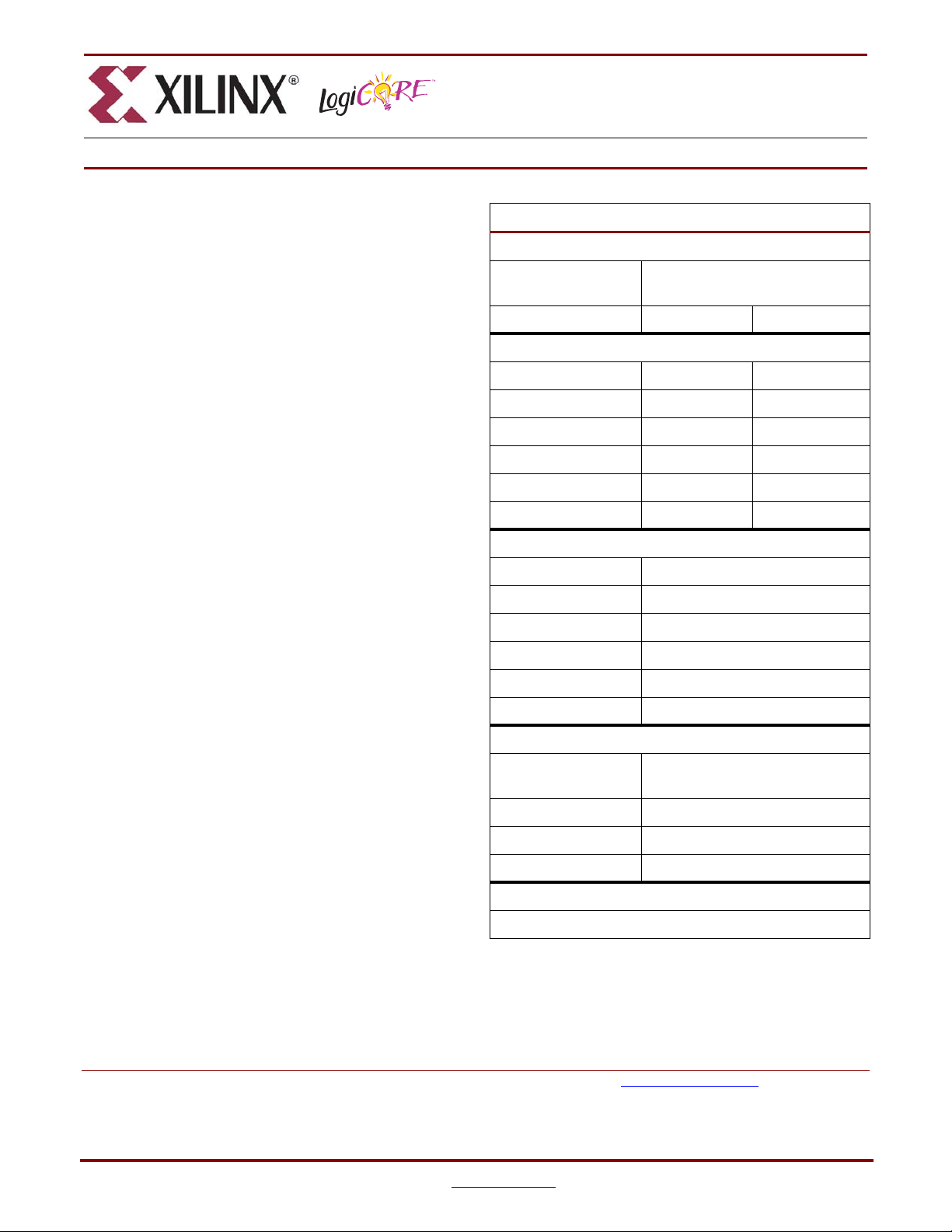
LogiCORE™ Facts
Core Specifics
Supported Device
Family
Version of Core plb_pci v1.00a
Resources Used
Virtex-IIP Min Max
I/O (PCI) 49 50
I/O (PLB-related) 397 433
LUTs 3350 3870
FFs 2570 2970
Block RAMs 8 8
Documentation Product Specification
Design File Formats VHDL
C
Provided with Core
Virtex™-II Pro, Virtex-4
ESS
Host bridge functionality (often called North bridge
functionality) is an optional functionality.
Configuration Read and Write PCI commands can be
performed from the PLB-side of the bridge. The PLB
PCI Bridge supports a 32-bit/33 MHz PCI bus only.
Exceptions to the support of PCI commands supported
by the v3.0 core are outlined in the
The PLB PCI Bridge design has parameters that allow
customers to configure the bridge to suit their
application. The parameterizable features of the design
are discussed in the
Bus Interface Parameters section.
A
Features section.
RLY AC
E
Constraints File example UCF-file
Verification N/A
Instantiation Template N/A
Reference Designs None
Design Tool Requirements
Xilinx Implementation
Tools
Verification N/A
Simulation ModelSim SE/EE 5.8d or later
Synthesis XST
Support
Support provided by Xilinx, Inc.
8.1.1i or later
© 2005 Xilinx, Inc. All rights reserved. All Xilinx trademarks, registered trademarks, patents, and further disclaimers are as listed at http://www.xilinx.com/legal.htm. All other trademarks and
registered trademarks are the property of their respective owners. All specifications are subject to change without notice.
NOTICE OF DISCLAIMER: Xilinx is providing this design, code, or information "as is." By providing the design, code, or information as one possible implementation of this feature, application,
or standard, Xilinx makes no representation that this implementation is free from any claims of infringement. You are responsible for obtaining any rights you may require for your implementation. Xilinx expressly disclaims any warranty whatsoever with respect to the adequacy of the implementation, including but not limited to any warranties or representations that this implementation is free from claims of infringement and any implied warranties of merchantability or fitness for a particular purpose.
DS508 March 21, 2006 www.xilinx.com 1
Product Specification
Page 2

PLB PCI Full Bridge (v1.00a)
Features
• Independent PLB and PCI clocks
• 33 MHz, 32-bit PCI bus support
• Utilizes two pairs of FIFOs to exploit the separate master and slave PLB IPIF modules.
• Includes a master IP module for remote PCI initiator transactions, which follows the protocol for
interfacing with the master IPIF module utilizing Xilinx LocalLink protocol. The PLB PCI Bridge
translates the PCI initiator request to PLB IPIF master transactions.
• Includes a slave IP module for remote PLB master transactions, which follows the protocol for
interfacing with the slave IPIF module utilizing Xilinx IPIC protocol. The PLB PCI Bridge translates
the PLB master request to PCI initiator transactions. The SRAM-like interface is utilized at the IPIC
interface for data transfers.
• The PLB IPIF slave attachment has a timer that limits the time for both read and write dataphase
operations to complete. When the timer expires, Sl_MErr signal is asserted. See PLB IPIF Product
Specification for details.
• Full bridge functionality
- PLB Master read and write of a remote PCI target (both single and burst)
- PCI Initiator read and write to a remote PLB slave (both single and multiple).
- I/O read and I/O write commands are supported only for PLB master read and writes of PCI
I/O space as designated by its associated memory designator parameter. All memory space on
the PLB-side is designated as memory space in the PCI sense, therefore, I/O commands cannot
be used to access memory on the PLB-side.
- Configuration read and writes are supported (including self-configuration transactions) only
when upper word address lines are utilized for IDSEL lines. The Configuration Read and Write
commands are automatically executed by writing to the Configuration Data Port Register. Data
in the Configuration Address Port Register and the Configuration Bus Number/Subordinate Bus
Number Register are used in execution of the configuration transaction per PCI 2.2 specification.
• PCI Memory Read Line (MRL) command is supported in which the v3.0 core is a target. MRL is
aliased to a Memory Read command which has a single data phase on the PCI.
• PCI Memory Write Invalidate (MWI) command is supported in which the v3.0 core is a target. The
v3.0 core does not support this command when it is an initiator. MWI is aliased to a Memory Write
command which has a single data phase on the PCI.
• Supports up to 6 PLB devices, in the sense defined by independent parameters and unique PLB
memory space for each device
- Each device has the following parameters: PLB BAR, high (upper) address, memory designator,
and translation for mapping PLB address space to PCI address space. Byte addressing integrity is
maintained by default in all transfers. Address translation is performed by high-order bit
substitution. High-order bit definition can be done with parameters or dynamically via registers.
EARLY ACCESS
• Supports up to 3 PCI devices (or BARs in PCI context) with unique memory PCI memory space.
The v3.0 core supports up to 3 PCI BAR.
- Each device has the following parameters: PCI BAR, length, memory designator, and translation
for mapping PCI address space to PLB address space. Byte addressing integrity is maintained by
2 www.xilinx.com DS508 March 21, 2006
Product Specification
Page 3

PLB PCI Full Bridge (v1.00a)
default in all transfers. Address translation is performed by high-order bit substitution.
High-order bit definition is defined only by parameters
•Registers include
- Interrupt and interrupt enable registers at different hierarchal levels
-Reset
- Configuration Address Port, Configuration Data Port and Bus Number/Subordinate Bus
Number
- High-order bits for PLB to PCI address translation
- Bridge Device number on PCI bus
• PLB-side Interrupts include
- PLB Master Read SERR and PERR
- PLB Master Read Target Abort
- PLB Master Write SERR and PERR
- PLB Master Write Target Abort
- PLB Master Write Master Abort
- PLB Master Burst Write Retry and Retry Disconnect
-PLB Master Burst Write Retry Timeout
- PCI Initiator Read and Write SERR
• Asynchronous FIFOs with backup capability
• Synchronization circuits for signals that cross time-domain boundaries
• Responds to the PCI latency timer
• Completes posted write operations prior to initiating new operations
• Signal set required for integrating a PCI bus arbiter in the FPGA with the PLB PCI bridge is
available at the top-level of the PLB PCI bridge module. The signal set includes PCLK, RST_N,
FRAME_I, REQ_N_toArb and IRDY_I
• Supports PCI clock generated in FPGA
• Parameterized control of IO-buffer insertion of INTR_A and REQ_N IO-buffers
• All address translations performed by high-order bit substitution. The number of bits substituted
depends on the address range
- Parameterized selection of IPIF BAR high-order bits defined by programmable registers for
dynamic translation operation or by parameters for reduced resource utilization
Y
L
ACCESS
AR
• Parameterized selection of device ID number (when configuration functionality is included)
defined by a programmable register for dynamic device number definition or by parameter to
reduce resource utilization
E
• The PLB PCI bridge does not have an integral DMA
• Input signal to provide the means to asynchronous asset INTR_A from a user supplied register (i.e.,
a PLB GPIO). The signal is Bus2PCI_INTR is an active high signal
• PCI Monitor output port to monitor PCI bus activity
DS508 March 21, 2006 www.xilinx.com 3
Product Specification
Page 4
PLB PCI Full Bridge (v1.00a)
System Reset
When the bridge is reset, both RST_N and PLB_reset must be simultaneously held at reset for at least
twenty clock periods of the slowest clock.
Evaluation Version
The PLB PCI Bridge is delivered with a hardware evaluation license. When programmed into a Xilinx
device, the core will function in hardware for about 8 hours at the typical frequency of operation. To use
the PLB PCI Bridge without this timeout limitation, a full license must be purchased.
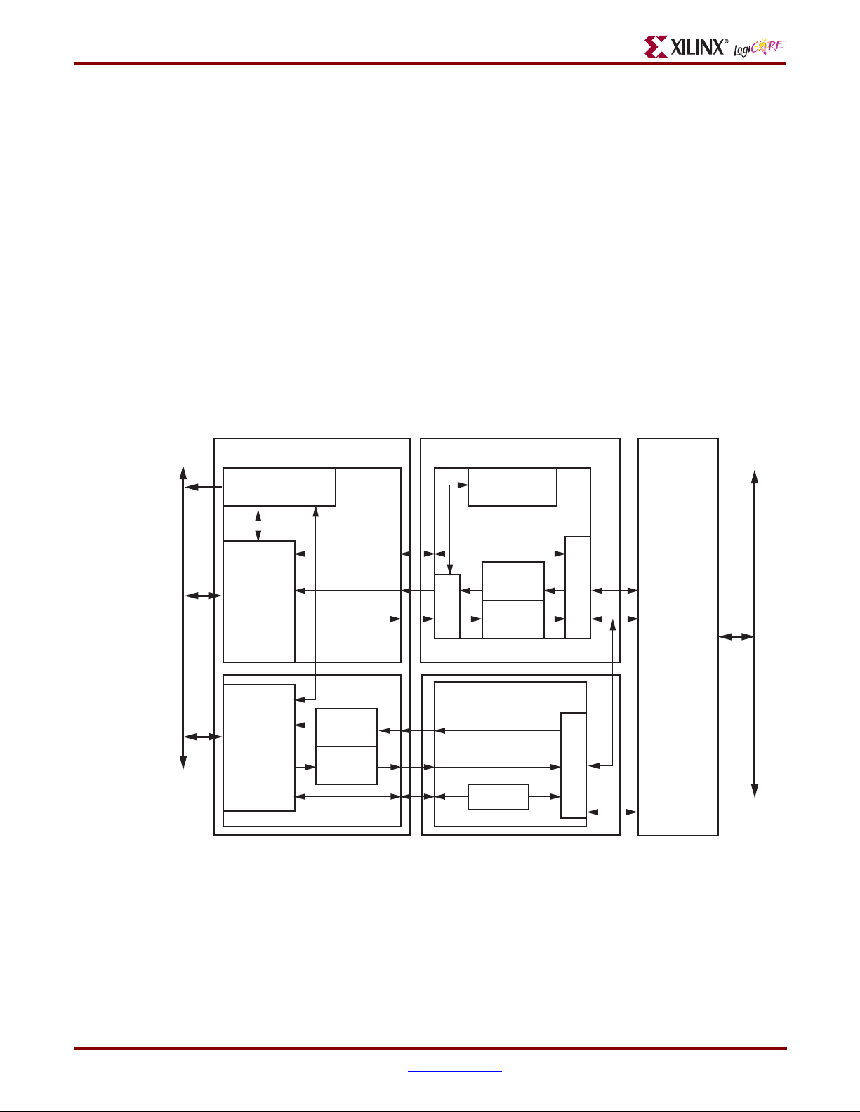
Functional Description
The PLB PCI Bridge design is shown in Figure 1 and described in the following sections. As shown,
PLB IPIF PCI Bridge is comprised of three main modules:
• The PLB IPIF (Processor Local Bus Intellectual Property InterFace). It interfaces to the PLB bus.
• The IPIF v3.0 Bridge. It interfaces between the PLB IPIF and the v3.0 core.
• The LogiCORE PCI32 Interface v3.0 core. It interfaces to the PCI bus.
Figure Top x-ref 1
Interrupt
Module
PLB IPIF
IPIF/V3 Bridge Xilinx
v3.0 PCI Core
Bridge
Registers
PLB Bus
Slave
Attachment
Master
Attachment
PCI2IPIF
FIFO
IPIF2PCI
FIFO
Slave SM
Master SM
PCI2IPIF
FIFO
IPIF2PCI
FIFO
Initiator
Target
PCI Bus
EARLY ACCESS
ds508_01_112205
Figure 1: PLB PCI Full Bridge Block Diagram
LogiCore Version 3.0 32-bit PCI Core Requirements
The PLB PCI bridge uses the 32-bit Xilinx LogiCore Version 3 IP core. Before the bridge can perform
transactions on the PCI bus, the v3.0 core must be configured via configuration transactions from either
the PCI-side or if configuration functionality is included in the bridge configuration, from the PLB-side.
Both a design guide and an implementation guide are available for the Xilinx LogiCore v3.0 PCI IP
4 www.xilinx.com DS508 March 21, 2006
Product Specification
Page 5

PLB PCI Full Bridge (v1.00a)
core. These documents detail the v3.0 core operation, including configuration cycles, and are available
from Xilinx.
As required by the LogiCORE v3.0 core, GNT_N must be asserted for two clock cycles to initiate a PCI
transaction by the PLB PCI Bridge.
Bus Interface Parameters
Because many features in the IPIF v3.0 Bridge design can be parameterized, the user can realize a PLB
PCI Full Bridge uniquely tailored while using only the resources required for the desired functionality.
This approach also achieves the best possible performance with the lowest resource usage.
shown the features that can be parameterized in the PLB PCI Bridge design.
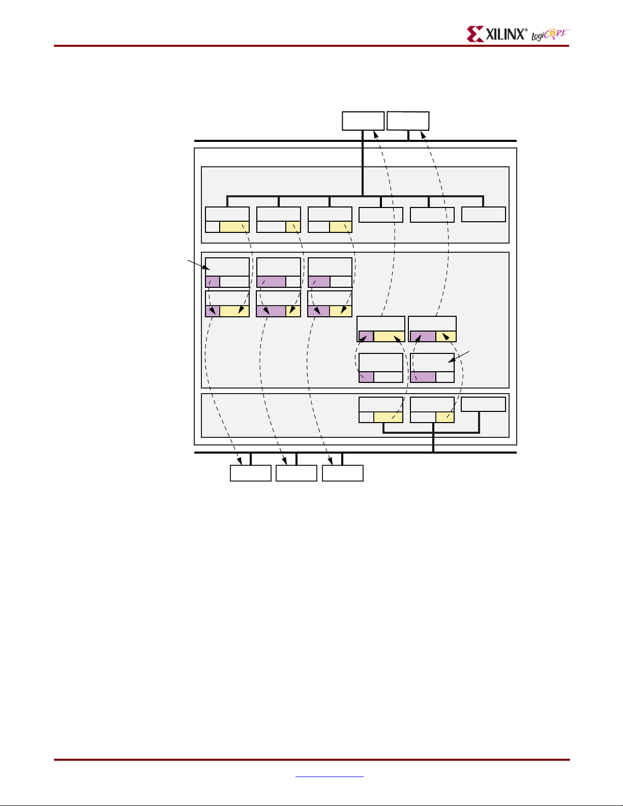
Address Translation
Address space on the PCI side that is accessible from the PLB side must be translated to a 2N contiguous
block on the PLB side. Up to six contiguous blocks are possible. Each block has parameters for base
address (C_IPIFBAR_N), high address, address translation vector, and memory designator (memory or
I/O).
All address space on the PLB side that is accessible from the PCI side must be translated to a maximum
of three 2
v3.0 core supports up to 3 BARs. Each block has parameters for length, which must be a 2
address translation vector. Only PCI memory space is supported.
N
contiguous blocks on the PCI side. Up to three blocks are possible because the LogiCore PCI
Tab le 1
N
range, and
Address translations in both directions are performed as follows:
• High-order address bits are substituted for the address vector before crossing to the other bus
domain. The number of high-order bits substituted in the PLB address presented to the bridge is
given by the number of bits that are the same between the C_IPIFBAR_N and C_
IPIF_HIGHADDR_N parameters. The number of high-order bits substituted in the PCI address
presented to the bridge for a translation from PCI to PLB domains is given by the bus width minus
the parameter C_PCIBAR_LEN_N.
• The low-order bits are transferred directly between bus domains. The bits substituted in a
translation from PLB to PCI domains can be selected via a parameter
(C_INCLUDE_BAROFFSET_REG) as either a parameter (C_IPIFBAR2PCIBAR_N) or a
programmable register for each BAR. The bits that are substituted for in a translation from PCI to
PLB domains is defined by a parameter (C_PCIBAR2IPIFBAR_M) for each BAR.
Figure 2 shows two sets of base address register (BAR) parameters and how they are used. The two sets
are independent sets: one set for the up to six PLB-side device (IPIFBAR) address ranges and another
set for the up to three PCI-side device (PCIBAR) address ranges.
This document includes three examples of how to use the two sets of base address register (BAR)
parameters:
Example 1, shown in Figure 2, outlines the use of the two sets of BAR parameters.
Example 2 outlines the use of the IPIFBAR parameters sets for the specific address translations of PLB
addresses within the range of a given IPIFBAR to a remote PCI address space.
E
AR
Y
L
ACCESS
DS508 March 21, 2006 www.xilinx.com 5
Product Specification
Page 6
PLB PCI Full Bridge (v1.00a)
Example 3 outlines the use of the PCIBAR parameter sets for the address translation of PCI addresses
within the range of a given PCIBAR to a remote PLB address space.
Figure Top x-ref 2
PLB Bus
PLB PCI Full Bridge
IPIF
C_IPIFBAR_NUM = 3
BAR_10
BAR_11
IPIFBAR_0
Note 1
PCI Bus
Figure 2: Translation of Addresses Bus-to-Bus with High-Order Bit Substitution
(high-order
bit sub)
Addr to PCI
IPIFBAR_1
(high-order
bit sub)
Addr to PCI
v3.0 LogiCORE
C_PCIBAR_NUM = 2
PBAR_21 PBAR_22PBAR_20
IPIFBAR_2
(high-order
bit sub)
Addr to PCI
IPIFBAR_3 IPIFBAR_4
IPIF to v3.0 LogiCORE Bridge
Addr to PLB
(high-order
bit sub)
PCIBAR_0
Addr to PLB
(high-order
bit sub)
PCIBAR_1
IPIFBAR_5
Note 2
PCIBAR_2
ds508_02_112205
Example 1
Because address translations are performed only when the PLB PCI Bridge is configured with FIFOs,
the example shown in
Figure 2 is for an PLB PCI Bridge configuration with FIFOs only. In this example, it
is assumed that C_INCLUDE_BAROFFSET_REG=0, therefore, the parameters C_IPIFBAR2PCIBAR_N
define the high-order bits for substitution in translating the address on the PLB bus to the PCI bus.
The PLB parameters are C_IPIFBAR_N, C_IPIF_HIGHADDR_N, and C_IPIFBAR2PCIBAR_N for N=0
EARLY ACCESS
to 5.
The PCI parameters are C_PCIBAR_LEN_M and C_PCIBAR2IPIFBAR_M for M=0 to 2.
Example 2
Example 2 shows of the settings of the two independent sets of base address register (BAR) parameters
for specifics of address translation of PLB addresses within the range of a given IPIFBAR to a remote
PCI address space. Note that this setting does not depend on the PCIBARs of the PLB PCI Bridge.
6 www.xilinx.com DS508 March 21, 2006
Product Specification
Page 7

PLB PCI Full Bridge (v1.00a)
As in example 1, it is assumed that the parameter C_INCLUDE_BAROFFSET_REG=0, therefore the
C_IPIFBAR2PCIBAR_N parameters define the address translation.
In this example, where C_IPIFBAR_NUM=4, the following assignments for each range are made:
C_IPIFBAR_0=0x12340000
C_IPIF_HIGHADDR_0=0x1234FFFF
C_IPIFBAR2PCIBAR_0=0x5671XXXX (Bits 16-31 are don’t cares)
C_IPIFBAR_1=0xABCDE000
C_IPIF_HIGHADDR_1=0xABCDFFFF
C_IPIFBAR2PCIBAR_1=0xFEDC0xXX (Bits 19-31 are don’t cares)
C_IPIFBAR_2=0xFE000000
C_IPIF_HIGHADDR_2=0xFFFFFFFF
C_IPIFBAR2PCIBAR_2=0x40xXXXXX (Bits 7-31 are don’t cares)
C_IPIFBAR_3=0x00000000
C_IPIF_HIGHADDR_3=0x0000007F
C_IPIFBAR2PCIBAR_3=8765438X (Bits 25-31 are don’t cares)
Accessing the PLB PCI Bridge IPIFBAR_0 with address 0x12340ABC on the PLB bus yields
0x56710ABC on the PCI bus.
Accessing the PLB PCI Bridge IPIFBAR_1 with address 0xABCDF123 on the PLB bus yields
0xFEDC1123 on the PCI bus.
Accessing the PLB PCI Bridge IPIFBAR_2 with address 0xFFFEDCBA on the PLB bus yields
0x41FEDCBA on the PCI bus.
Accessing the PLB PCI Bridge IPIFBAR_3 with address 0x00000071 on the PLB bus yields
Ox876543F1 on the PCI bus.
Example 3
Example 3 outlines address translation of PCI addresses within the range of a given PCIBAR to PLB
address space. Note that this translation is independent of the PLB PCI Bridge IPIF BARs.
The parameters C_PCIBAR2IPIFBAR_M parameters define the address translation for all
C_PCIBAR_NUM.
In this example, where C_PCIBAR_NUM=2, the following range assignments are made:
BAR 0 is set to 0xABCDE800 by host
C_PCIBAR_LEN_0=11
C_PCIBAR2IPIFBAR_0=0x123450XX (Bits 21-31 are don’t cares)
BAR 1 is set to 0x12000000 by host
C_PCIBAR_LEN_1=25
C_PCIBAR2IPIFBAR_1=0xFEXXXXXX (Bits 7-31 are don’t cares)
Accessing the PLB PCI Bridge PCIBAR_0 with address 0xABCDEFF4 on the PCI bus yields
0x123457F4 on the PLB bus.
E
AR
Y
L
ACCESS
DS508 March 21, 2006 www.xilinx.com 7
Product Specification
Page 8

PLB PCI Full Bridge (v1.00a)
Accessing the PLB PCI Bridge PCIBAR_1 with address 0x1235FEDC on the PCI bus yields
0xFE35FEDC on the PLB bus.
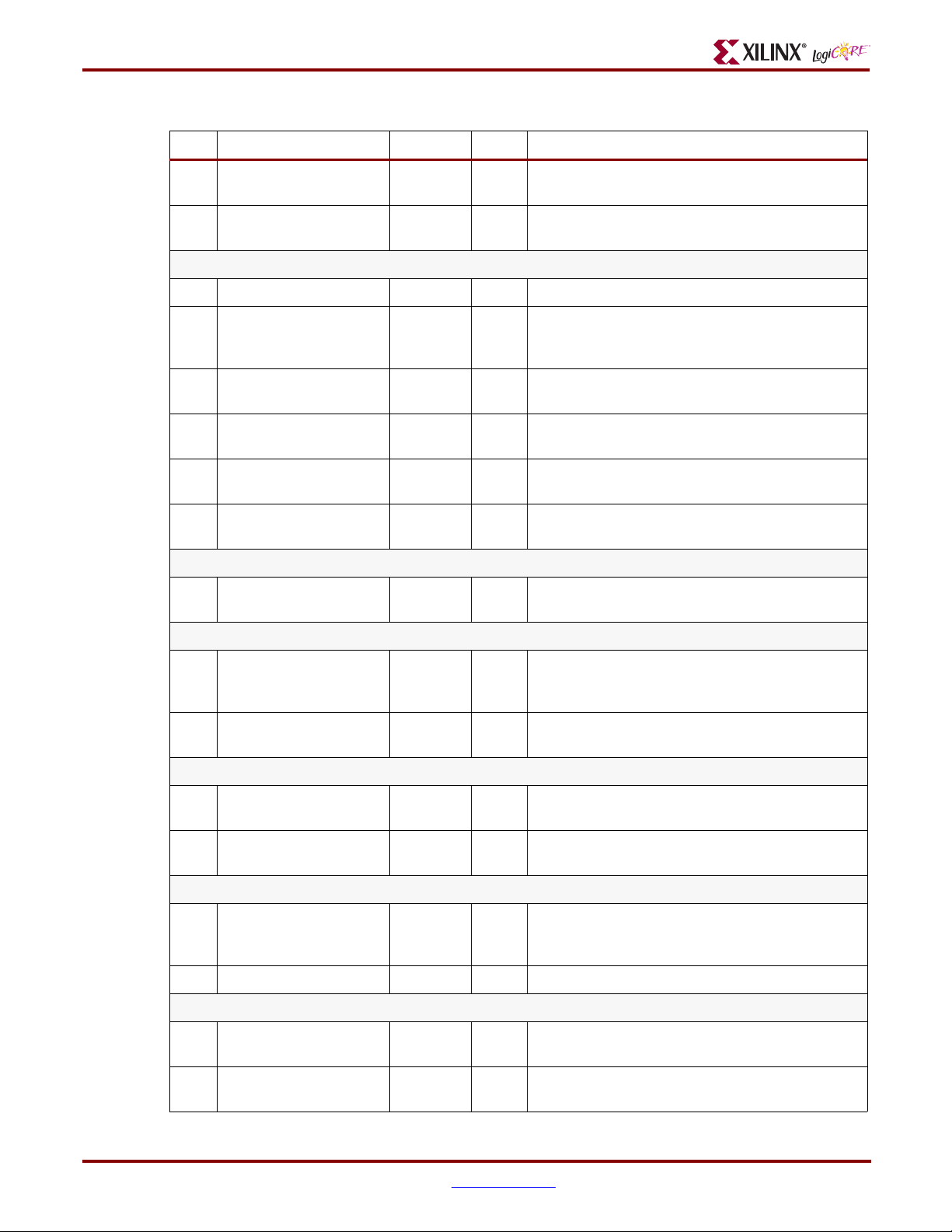
Table 1: PLB PCI Bridge Interface Design Parameters
Generic
G1 Number of IPIF devices
G2 IPIF device 0 BAR C_IPIFBAR_0 Valid PLB address
G3
G4
G5
Feature /
Description
IPIF BAR high address 0C_IPIFBAR_
PCI BAR to which IPIF
BAR 0 is mapped
unless
C_INCLUDE_BAROFF
SET_REG = 1
IPIF BAR 0 memory
designator
Parameter
Name
Bridge Features Parameter Group
C_IPIFBAR
_NUM
HIGHADDR_0
C_IPIFBAR2
PCIBAR_0
C_IPIF_SPACE
TYPE_0
1
Allowable Values
1-6; Parameters listed
below corresponding to
unused BARs are
ignored, but must be
valid values. BAR label
0 is the required bar for
all values 1-6 and the
index increments from 0
as BARs are added
Valid PLB address
Vector of length
C_PLB_AWIDTH
0 = I/O space
1 = Memory space
(1)
(1)
Default
Val ue
6 integer
0xFFFFFFFF
0x00000000
0xFFFFFFFF
1 integer
VHDL
Type
std_logic_
vector
std_logic_
vector
std_logic_
vector
G6 IPIF device 1 BAR C_IPIFBAR_1 Valid PLB address
G7
G8
G9
G10 IPIF device 2 BAR C_IPIFBAR_2 Valid PLB address
G11
G12
IPIF BAR high address 1C_IPIFBAR_
HIGHADDR_1
PCI BAR to which IPIF
BAR 1 is mapped
unless
C_INCLUDE_BAROFF
SET_REG = 1
IPIF BAR 1 memory
designator
C_IPIFBAR2
PCIBAR_1
C_IPIF_SPACE
TYPE_1
Valid PLB address
Vector of length
C_PLB_AWIDTH
0 = I/O space
1 = Memory space
EARLY ACCESS
IPIF BAR high address 2C_IPIFBAR_
HIGHADDR_2
PCI BAR to which IPIF
BAR 2 is mapped
unless
C_INCLUDE_BAROFF
SET_
REG = 1
C_IPIFBAR2
PCIBAR_2
Valid PLB address
Vector of length
C_PLB_AWIDTH
(1)
(1)
(1)
(1)
0xFFFFFFFF
0x00000000
0xFFFFFFFF
1 integer
0xFFFFFFFF
0x00000000
0xFFFFFFFF
std_logic_
vector
std_logic_
vector
std_logic_
vector
std_logic_
vector
std_logic_
vector
std_logic_
vector
8 www.xilinx.com DS508 March 21, 2006
Product Specification
Page 9

Table 1: PLB PCI Bridge Interface Design Parameters (Contd)
PLB PCI Full Bridge (v1.00a)
Generic
G13
G14 IPIF device 3 BAR C_IPIFBAR_3 Valid PLB address
G15
G16
G17
G18 IPIF device 4 BAR C_IPIFBAR_4 Valid PLB address
G19
G20
Feature /
Description
IPIF BAR 2 memory
designator
IPIF BAR high
address 3
PCI BAR to which IPIF
BAR 3 is mapped
unless
C_INCLUDE_BAROFF
SET_REG = 1.
IPIF BAR 3 memory
designator
IPIF BAR high
address 4
PCI BAR to which IPIF
BAR 4 is mapped
unless
C_INCLUDE_BAROFF
SET_REG = 1
Parameter
Name
C_IPIF_SPACE
TYPE_2
C_IPIFBAR_
HIGHADDR_3
C_IPIFBAR2
PCIBAR_3
C_IPIF_SPACE
TYPE_3
C_IPIFBAR_
HIGHADDR_4
C_IPIFBAR2
PCIBAR_4
Allowable Values
0 = I/O space
1 = Memory space
Valid PLB address
Vector of length
C_PLB_AWIDTH
0 = I/O space
1 = Memory space
Valid PLB address
Vector of length
C_PLB_AWIDTH
(1), (2)
(1), (2)
(1), (2)
(1), (2)
Default
Val ue
1 integer
0xFFFFFFFF
0x00000000
0xFFFFFFFF
1 integer
0xFFFFFFFF
0x00000000
0xFFFFFFFF
VHDL
Type
std_logic_
vector
std_logic_
vector
std_logic_
vector
std_logic_
vector
std_logic_
vector
std_logic_
vector
G21
G22 IPIF device 5 BAR C_IPIFBAR_5 Valid PLB address
G23
G24
G25
IPIF BAR 4 memory
designator
IPIF BAR high
address 5
PCI BAR to which IPIF
BAR 5 is mapped
unless
C_INCLUDE_BAROFF
SET_
REG = 1
IPIF BAR 5 memory
designator
C_IPIF_SPACE
TYPE_4
C_IPIFBAR_
HIGHADDR_5
Y
L
C_IPIFBAR2
PCIBAR_5
C_IPIF_SPACE
TYPE_5
0 = I/O space
1 = Memory space
ACCESS
Valid PLB address
Vector of length
C_PLB_AWIDTH
0 = I/O space
1 = Memory space
AR
1-3; Parameters listed
below corresponding to
E
G26 Number of PCI devices
C_PCIBAR_
NUM
unused BARs are
ignored, but must be
valid values. BAR label
0 is the required bar for
all values 1-3 and the
index increments from 0
as BARs are added
(1), (2)
(1), (2)
1 integer
0xFFFFFFFF
0x00000000
0xFFFFFFFF
1 integer
3 integer
std_logic_
vector
std_logic_
vector
std_logic_
vector
DS508 March 21, 2006 www.xilinx.com 9
Product Specification
Page 10

PLB PCI Full Bridge (v1.00a)
Table 1: PLB PCI Bridge Interface Design Parameters (Contd)
Generic
G27
G28
G29
G30
G31
G32
G33 PCI address bus width
G34 PCI data bus width
Feature /
Description
IPIF BAR to which PCI
BAR 0
is mapped
Power of 2 in the size in
bytes of PCI BAR 0
space
IPIF BAR to which PCI
BAR 1 is mapped
Power of 2 in the size in
bytes of PCI BAR 1
space
IPIF BAR to which PCI
BAR 2 is mapped
Power of 2 in the size in
bytes of PCI BAR 2
space
Parameter
Name
C_PCIBAR2
IPIFBAR_0
C_PCIBAR_
LEN_0
C_PCIBAR2IPI
FBAR_1
C_PCIBAR_
LEN_1
C_PCIBAR2
IPIFBAR_2
C_PCIBAR_
LEN_2
C_PCI_ABUS_
WIDTH
C_PCI_DBUS_
WIDTH
Allowable Values
Vector of length
C_PLB_AWIDTH
5 to 29 16 integer
Vector of length
C_PLB_AWIDTH
5 to 29 16 integer
Vector of length
C_PLB_AWIDTH
5 to 29 16 integer
32 32 integer
32 32 integer
Default
Val ue
0x00000000
0x00000000
0x00000000
VHDL
Type
std_logic_
vector
std_logic_
vector
std_logic_
vector
G35
G36
G37
G38
G39
Both PCI2IPIF FIFO
address bus widths.
Usable depth is
2^C_PCI2IPIF_FIFO_A
BUS_WIDTH - 3
Both IPIF2PCI FIFO
address bus widths.
Usable depth is
2^C_IPIF2PCI_FIFO_A
BUS_WIDTH - 3
Include explicit
instantiation of INTR_A
io-buffer (must be 1 to
include io-buffer)
Include explicit
instantiation of REQ_N
EARLY ACCESS
io-buffer (must be 1 to
include io-buffer)
Minimum PCI2IPIF
FIFO occupancy level
that triggers the bridge
to initiate a prefetch PCI
read of a remote PCI
agent
C_PCI2IPIF_
FIFO_ABUS_
WIDTH
C_IPIF2PCI_
FIFO_ABUS_
WIDTH
C_INCLUDE_
INTR_A_BUF
C_INCLUDE_
REQ_N_BUF
C_TRIG_PCI_
READ_OCC_
LEVEL
4-14 9 integer
4-14 9 integer
0 = not included
1 = included
0 = not included
1 = included
5 to the lesser of 24 or
the PCI2IPIF FIFO
DEPTH-3. PCI2IPIF
FIFO DEPTH given by
2^C_PCI2IPIF_FIFO_
ABUS_WIDTH
1 integer
1 integer
32 integer
10 www.xilinx.com DS508 March 21, 2006
Product Specification
Page 11

Table 1: PLB PCI Bridge Interface Design Parameters (Contd)
PLB PCI Full Bridge (v1.00a)
Generic
G40
G41
G42
Feature /
Description
PCI2IPIF FIFO
occupancy level in
double words that
triggers the bridge to
initiate an IPIF burst
write to remote PLB
device
IPIF2PCI FIFO
occupancy level that
starts data transfer
(Both as initiator and
target on PCI) to PCI
agent with multiple data
phases per transfer
(must meet 16 PCI
period maximum).
Minimum IPIF2PCI
FIFO occupancy level
that triggers bridge to
initiate a prefetch IPIF
read of a remote PLB
slave
Parameter
Name
C_TRIG_IPIF_
WRBURST_
OCC_LEVEL
C_TRIG_PCI_
DATA_XFER_
OCC_LEVEL
C_TRIG_IPIF_
READ_OCC_
LEVEL
Allowable Values
2 to the lesser of 24 or
the PCI2IPIF FIFO
DEPTH-3. PCI2IPIF
FIFO DEPTH given by
2^C_PCI2IPIF_FIFO_A
BUS_WIDTH
2 to the lesser of 24 or
the IPIF2PCI FIFO
DEPTH-3. IPIF2PCI
FIFO DEPH given by
2^C_IPIF2PCI_FIFO_
ABUS_WIDTH
2 to the lesser of 24 or
the IPIF2PCI FIFO
DEPTH-3. IPIF2PCI
FIFO DEPH given by
2^C_IPIF2PCI_FIFO_
ABUS_WIDTH
Default
Val ue
8 integer
8 integer
16 integer
VHDL
Type
Number of PCI retry
G43
G44
G45
G46 Device base address
G47
G48
G49
attempts in IPIF
posted-write operations
Number of PCI clock
periods between retries
in posted- write
operations
Number of IPIF retry
attempts in
posted-write PCI
initiator operations
Device absolute high
address
Include the registers for
high-order bits to be
AR
substituted in
translation
E
Include the register for
local bridge device
number when
configuration
functionality
(C_INCLUDE_PCI_CO
NFIG =1) is included
C_NUM_PCI_R
ETRIES_IN_
WRITES
C_NUM_PCI_P
RDS_BETWN_
RETRIES_IN_
WRITES
C_NUM_IPIF_
RETRIES_IN_
Y
WRITES
L
C_BASE
ADDR
C_HIGHADDR Valid PLB address
C_INCLUDE_
BAROFFSET_
REG
C_INCLUDE_D
EVNUM_REG
Any integer 3 integer
Any integer 6 integer
ACCESS
Any integer 6 integer
Valid PLB address
1 = include
0 = exclude
1 = include
0 = exclude
(1), (2)
(1), (2)
0xFFFFFFFF
0x00000000
0 integer
0 integer
std_logic_
vector
std_logic_
vector
DS508 March 21, 2006 www.xilinx.com 11
Product Specification
Page 12

PLB PCI Full Bridge (v1.00a)
Table 1: PLB PCI Bridge Interface Design Parameters (Contd)
Generic
G50
G51
G52
G53
Feature /
Description
Number of IDELAY
controllers instantiated.
Ignored it not Virtex-4
Includes IDELAY
primitive on GNT_N.
Set by tcl-scripts and
ignored if not Virtex-4.
Provides a means for
BSB to pass LOC
coordinates for
IDELAYCTRLs for a
given board to
EDK and is optional for
user to set LOC
constraints. This
parameter has no
impact on bridge
functionality.
PCI Configuration
Space Header Device IDC_DEVICE_ID 16-bit vector 0x0000
Parameter
Name
C_NUM_
IDELAYCTRL
C_INCLUDE_
GNT_DELAY
C_IDELAY
CTRL_LOC
v3.0 Core Parameters Group
Allowable Values
2-6
(Virtex-4 only)
1=Include IDELAY
primitive
(Virtex-4 only)
0=No IDELAY primitive
See Device
Implementation section,
subsection Virtex-4
Support for allowed
values
Default
Val ue
2 integer
0 integer
NOT_SET string
VHDL
Type
std_logic_
vector
G54
G55
G56
G57
G58
G59
G60
PCI Configuration
Space Header Vendor
ID
PCI Configuration
Space Header Class
Code
PCI Configuration
Space Header Rev ID
PCI Configuration
Space Header
Subsystem ID
PCI Configuration
Space Header
Subsystem Vendor ID
EARLY ACCESS
PCI Configuration
Space Header
Maximum Latency
PCI Configuration
Space Header
Minimum Grant
C_VENDOR_
ID
C_CLASS_
CODE
C_REV_ID 8-bit vector 0x00
C_SUB
SYSTEM_ID
C_SUBSYSTE
M_VENDOR_
C_MAX_LAT 8-bit vector 0x0F
C_MIN_GNT 8-bit vector 0x04
Configuration
16-bit vector 0x0000
24-bit vector 0x000000
16-bit vector 0x0000
ID16-bit vector 0x0000
std_logic_
vector
std_logic_
vector
std_logic_
vector
std_logic_
vector
std_logic_
vector
std_logic_
vector
std_logic_
vector
12 www.xilinx.com DS508 March 21, 2006
Product Specification
Page 13

Table 1: PLB PCI Bridge Interface Design Parameters (Contd)
PLB PCI Full Bridge (v1.00a)
Generic
G61
G62
G63
G64
G65
G66 PLB Address width
G67 PLB Data width
Feature /
Description
Include configuration
functionality via IPIF
transactions
Number of IDSEL
signals supported
PCI address bit that PCI
v3.0 core IDSEL is
connected to
PLB master ID bus
width (set automatically
by XPS)
Number of masters on
PLB bus (set
automatically by XPS)
Parameter
Name
C_INCLUDE_
PCI_CONFIG
C_NUM_
IDSEL
C_BRIDGE_
IDSEL_ADDR_
BIT
IPIF Parameters Group
C_PLB_MID_
WIDTH
C_PLB_NUM_
MASTERS
C_PLB_
AWIDTH
C_PLB_
DWIDTH
Allowable Values
0 = Not included
1 = Included
1 to 16 8 integer
31 down to 16
Must be <= 15 +
C_NUM_IDSEL.
AD(31 down to 0) index
labeling
log2(C_PLB_NUM_MA
STERS)
1-16 8 integer
32 (only allowed value 32 integer
64 (only allowed value 64 integer
Default
Val ue
1 integer
16 integer
3 integer
VHDL
Type
G68
Notes:
1. The range specified must comprise a complete, contiguous power of two range, such that the range = 2n and
the n least significant bits of the Base Address are zero.
2. The minimum address range specified by C_BASEADDR and C_HIGHADDR must be at least 0x1FF.
C_BASEADDR must be a multiple of the range, where the range is C_HIGHADDR - C_BASEADDR + 1.
Specifies the target
technology
C_FAMILY
See PLB IPIF data
sheet
virtex2 string
ACCESS
Y
L
AR
E
DS508 March 21, 2006 www.xilinx.com 13
Product Specification
Page 14

PLB PCI Full Bridge (v1.00a)
PLB PCI Bus Interface I/O Signals
The I/O signals for the PLB PCI Bridge are listed in Tab le 2. The interfaces referenced in this table are
shown in Figure 1 in the PLB PCI Bridge block diagram.
Table 2: PLB PCI Bridge I/O Signals
Port Signal Name Interface I/O Description
P1 IP2INTC_Irpt Internal O Interrupt from IP to the Interrupt Controller
P2 PLB_Clk PLB Bus I PLB main bus clock. See table note 1.
P3 PLB_Rst PLB Bus I PLB main bus reset. See table note 1.
PLB_ABus(0:C_PLB_
P4
AWIDTH-1)
P5 PLB_PAValid PLB Bus I
PLB_masterID(0:C_PLB
P6
_MID_WIDTH-1)
System Signals
PLB Signals
PLB Bus I Note 1 applies from P4 to P53.
PLB Bus I
P7 PLB_abort PLB Bus I
P8 PLB_RNW PLB Bus I
PLB_BE(0:[C_PLB_DWI
P9
DTH/8]-1)
P10 PLB_MSize(0:1) PLB Bus I
P11 PLB_size(0:3) PLB Bus I
P12 PLB_type(0:2) PLB Bus I
PLB_wrDBus(0:C_PLB_
P13
DWIDTH-1)
P14 PLB_wrBurst PLB Bus I
P15 PLB_rdBurst PLB Bus I
P16 Sl_addAck PLB Bus O
P17 Sl_SSize(0:1) PLB Bus O
P18 Sl_wait PLB Bus O
P19 Sl_rearbitrate PLB Bus O
P20 Sl_wrDAck PLB Bus O
P21 Sl_wrComp PLB Bus O
EARLY ACCESS
PLB Bus I
PLB Bus I
P22 Sl_wrBTerm PLB Bus O
Sl_rdDBus(0:C_PLB_D
P23
WIDTH-1)
P24 Sl_rdWdAddr(0:3) PLB Bus O
P25 Sl_rdDAck PLB Bus O
P26 Sl_rdComp PLB Bus O
14 www.xilinx.com DS508 March 21, 2006
PLB Bus O
Product Specification
Page 15

PLB PCI Full Bridge (v1.00a)
Table 2: PLB PCI Bridge I/O Signals (Contd)
Port Signal Name Interface I/O Description
P27 Sl_rdBTerm PLB Bus O
Sl_MBusy(0:C_PLB_NU
P28
M_MASTERS-1)
Sl_MErr(0:C_PLB_NUM
P29
_MASTERS-1)
P30 PLB_MAddrAck PLB Bus I
P31 PLB_MSSize(0:1) PLB Bus I
P32 PLB_MRearbitrate PLB Bus I
P33 PLB_MBusy PLB Bus I
P34 PLB_MErr PLB Bus I
P35 PLB_MWrDAck PLB Bus I
PLB_MRdDBus(0:C_PL
P36
B_DWIDTH-1)
PLB Bus O
PLB Bus O
PLB Bus I
P37 PLB_MRdWdAddr(0:3) PLB Bus I
P38 PLB_MRdDAck PLB Bus I
P39 PLB_MRdBTerm PLB Bus I
P40 PLB_MWrBTerm PLB Bus I
P41 M_request PLB Bus O
P42 M_priority PLB Bus O
P43 M_buslock PLB Bus O
P44 M_RNW PLB Bus O
M_BE(0:[C_PLB_DWIDT
P45
H/8]-1)
P46 M_MSize(0:1) PLB Bus O
P47 M_size(0:3) PLB Bus O
P48 M_type(0:2) PLB Bus O
P49 M_abort PLB Bus O
M_ABus(0:C_PLB_AWI
P50
DTH-1)
P51
M_wrDBus(0:C_PLB_D
WIDTH-1)
AR
PLB Bus O
Y
L
PLB Bus O
PLB Bus O
ACCESS
P52 M_wrBurst PLB Bus O
P53 M_rdBurst PLB Bus O Table note 1 applies from P53 to P4.
P54
DS508 March 21, 2006 www.xilinx.com 15
Product Specification
E
AD[C_PCI_DBUS_WIDT
H-1:0]
PCI Address and Data Path Signals
PCI Bus I/O Time-multiplexed address and data bus
Page 16
PLB PCI Full Bridge (v1.00a)
Table 2: PLB PCI Bridge I/O Signals (Contd)
Port Signal Name Interface I/O Description
CBE[(C_PCI_DBUS_WI
P55
DTH/8)-1:0]
PCI Bus I/O Time-multiplexed bus command and byte enable bus
P56 PA R PCI Bus I/O
PCI Transaction Control Signals
P57 FRAME_N PCI Bus I/O Driven by an initiator to indicate a bus transaction
P58 DEVSEL_N PCI Bus I/O
P59 TRDY_N PCI Bus I/O
P60 IRDY_N PCI Bus I/O
P61 STOP_N PCI Bus I/O
P62 IDSEL PCI Bus I
PCI Interrupt Signals
P63 INTR_A PCI Bus O
PCI Error Signals
P64 PERR_N PCI Bus I/O
Generates and checks even parity across AD and
CBE
Indicates that a target has decoded the address
presented during the address phase and is claiming
the transaction
Indicates that the target is ready to complete the
current data phase
Indicates that the initiator is ready to complete the
current data phase
Indicates that the target has requested to stop the
current transaction
Indicates that the interface is the target of a
configuration cycle
Indicates that LogiCORE PCI interface requests an
interrupt
Indicates that a parity error was detected while the
LogiCORE PCI interface was the target of a write
transfer or the initiator of a read transfer
P65 SERR_N PCI Bus I/O
PCI Arbitration Signals
P66 REQ_N PCI Bus O
P67 GNT_N PCI Bus I
PCI System Signals
EARLY ACCESS
P68 RST_N PCI Bus I
P69 PCLK PCI Bus I PCI bus clock signal
PCI Bus Internal Arbiter Signals
P70 REQ_N_toArb Internal O
P71 FRAME_I Internal O
Indicates that a parity error was detected during an
address cycle, except during special cycles
Indicates to the arbiter that the LogiCORE PCI
initiator requests access to the bus
Indicates that the arbiter has granted the bus to the
LogiCORE PCI initiator
PCI bus reset signal is used to bring PCI-specific
registers, sequences, and signals to a consistent
state
Input from PCI Bus REQ_N available at top-level as
output from bridge
Input from PCI Bus FRAME_N availalble at top-level
as output from bridge
16 www.xilinx.com DS508 March 21, 2006
Product Specification
Page 17
PLB PCI Full Bridge (v1.00a)
Table 2: PLB PCI Bridge I/O Signals (Contd)
Port Signal Name Interface I/O Description
P72 IRDY_I Internal O
PCI 64-bit Extensions (reserved for future support of 64-bit PCI)
P73 PA R6 4 PCI Bus I/O
P74 ACK64_N PCI Bus I/O
P75 REQ64_N PCI Bus I/O
User Asserted PCI Interrupt Signal
P76 Bus2PCI_INTR Internal I
Virtex-4 Only, IDELAY Clock
P77 RCLK Internal I
PCI Bus Monitoring Debug Vector Signal
P78 PCI_monitor(0:47) Internal O Output vector to monitor PCI Bus.
Input from PCI Bus IRDY_N availalble at top-level as
output from bridge
Generates and checks even parity across AD[63:32]
and CBE[7:4]
Indicates that a target has decoded the address
presented during the address phase and is claiming
the transaction as a 64-bit target
Driven by the initiator to indicate a 64-bit bus
transaction
Active high signal to asynchronously assert INTR_A.
Inverted signal drives INTR_N user application input
of v3.0 core. See v3.0 core documents for details on
INTR_N functionality.
200 MHz clock input to IDELAY elements of Virtex-4
buffers. Ignored if not Virtex-4 architecture.
Notes:
1. This signal’s function and timing are defined in the IBM 64-Bit Processor Local Bus Architecture Specification
Version 3.5.
The REQ_N_toArb facilitates an interface to an internal (i.e., in the FPGA) pci arbiter. The v3.0 input
buffer for GNT_N is removed. This allows an internal connection to GNT_N when using an internal
arbiter. When an external arbiter is used, GNT_N_fromArb is not needed.
REQ_N is a 3-stated I/O. The REQ_N_toArb port is available to maintain a v3.0 core-like interface. The
REQ_N_toArb port allows the use of the same port list for PCI bus interface and the ucf-file for the v3.0
core is the standard file.
The v3.0 core requires that GNT_N be asserted for two clock cycles to initiate a transaction upon
receiving grants.
Bus2PCI_INTR is an active High signal. It allows asynchronous assertion of INTR_A on the PCI bus.
The signal is driven by user supplied circuitry (i.e., a PLB GPIO IP core). If it is not connected in the
mhs-file, then EDK 8.1 tools will tie the signal Low. The signal is inverted in the PLB PCI Bridge and
AND’d with the bridge interrupt signal (active Low) to drive the INTR_N input of the v3.0 core. This
signal then asynchronously drives INTR_A on the PCI bus. See the v3.0 core specifications on INTR_A
behavior relative to v3.0 input INTR_N. The v3.0 core command register interrupt disable bit controls the
INTR_A operation and v3.0 core status register Interrupt status bit flags if v3.0 core INTR_A is asserted.
E
AR
Y
L
ACCESS
DS508 March 21, 2006 www.xilinx.com 17
Product Specification
Page 18

PLB PCI Full Bridge (v1.00a)
Port and Parameter Dependencies
The dependencies between the IPI v3.0 Bridge design port (i.e., I/O signals) and parameters are shown
in
Tab le 1.
Table 3: PLB PCI Bridge Parameters-Port Dependencies
Generic Parameter Affects Depends Description
G1 C_IPIFBAR_NUM G5-G25
G2 C_IPIFBAR_0 G3 G3
Bridge Features Parameter Group
The set of PLB/IPIF BAR-parameters of
N = 0 to C_IPIFBAR_NUM-1 are
meaningful. When C_IPIFBAR_NUM <
6, the parameters of N =
C_IPIFBAR_NUM up to and including 5
have no effect. If C_IPIFBAR_NUM = 6,
the set of PLB/IPIF BAR-parameters of N
= 0 to 5 are all meaningful (i.e., G2-G25
are meaningful).
G2 to G3 define range in PLB-memory
space that is responded to by this device
(IPIF BAR)
G2 to G3 define range in PLB-memory
G3 C_IPIFBAR_HIGHADDR_0 G2 G2
G4 C_IPIFBAR2PCIBAR_0
G5 C_IPIF_SPACETYPE_0
G6 C_IPIFBAR_1 G7 G1 and G7
G7 C_IPIFBAR_HIGHADDR_1 G6 G1 and G6
G8 C_IPIFBAR2PCIBAR_1
G9 C_IPIF_SPACETYPE_1 G1 Meaningful only if G1>1
G2, G3 and
G48
G1, G6, G7
and G48
EARLY ACCESS
G10 C_IPIFBAR_2 G11
G1 and
G11
space that is responded to by this device
(IPIF BAR)
Meaningful only if G48 = 0 and in this
case only high-order bits that are the
same in G2 and G3 are meaningful.
Meaningful only if G1>1, then G6 to G7
define the range in PLB-memory space
that is responded to by this device (IPIF
BAR)
Meaningful only if G1>1, then G6 to G7
define the range in PLB-memory space
that is responded to by this device (IPIF
BAR)
Meaningful only if G48 = 0 and G1>1. In
this case only high-order bits that are the
same in G6 and G7 are meaningful.
Meaningful only if G1>2, then G10 to
G11 define the range in PLB-memory
space that is responded to by this device
(IPIF BAR)
Meaningful only if G1>2, then G10 to
G11 C_IPIFBAR_HIGHADDR_2 G10
18 www.xilinx.com DS508 March 21, 2006
G1 and
G10
G11 define the range in PLB-memory
space that is responded to by this device
(IPIF BAR)
Product Specification
Page 19

PLB PCI Full Bridge (v1.00a)
Table 3: PLB PCI Bridge Parameters-Port Dependencies (Contd)
Generic Parameter Affects Depends Description
G1, G10,
G12 C_IPIFBAR2PCIBAR_2
G13 C_IPIF_SPACETYPE_2 G1 Meaningful only if G1>2
G14 C_IPIFBAR_3 G15
G15 C_IPIFBAR_HIGHADDR_3 G14
G16 C_IPIFBAR2PCIBAR_3
G17 C_IPIF_SPACETYPE_3 G1 Meaningful only if G1>3
G18 C_IPIFBAR_4 G19
G19 C_IPIFBAR_HIGHADDR_4 G18
G11 and
G48
G1 and
G15
G1 and
G14
G1, G14,
G15 and
G48
G1 and
G19
G1 and
G18
Meaningful only if G48 = 0 and G1>2. In
this case only high-order bits that are the
same in G10 and G11 are meaningful.
Meaningful only if G1>3, then G14 to
G15 define the range in PLB-memory
space that is responded to by this device
(IPIF BAR)
Meaningful only if G1>3, then G14 to
G15 define the range in PLB-memory
space that is responded to by this device
(IPIF BAR)
Meaningful only if G48 = 0 and G1>3. In
this case only high-order bits that are the
same in G14 and G15 are meaningful.
Meaningful only if G1>4, then G18 to
G19 define the range in PLB-memory
space that is responded to by this device
(IPIF BAR)
Meaningful only if G1>4, then G18 to
G19 define the range in PLB-memory
space that is responded to by this device
(IPIF BAR)
G1, G18,
G20 C_IPIFBAR2PCIBAR_4
G21 C_IPIF_SPACETYPE_4 G1 Meaningful only if G1>4
G22 C_IPIFBAR_5 G23
Y
G19 and
G48
ACCESS
G1 and
G23
L
G23 C_IPIFBAR_HIGHADDR_5 G22
G24 C_IPIFBAR2PCIBAR_5
G25 C_IPIF_SPACETYPE_5 G1 Meaningful only if G1=6
E
AR
G1 and
G22
G1, G22,
G23 and
G48
Meaningful only if G48 = 0 and G1>4. In
this case only high-order bits that are the
same in G6 and G7 are meaningful.
Meaningful only if G1=6, then G6 to G7
define the range in PLB-memory space
that is responded to by this device (IPIF
BAR)
Meaningful only if G1=6, then G6 to G7
define the range in PLB-memory space
that is responded to by this device (IPIF
BAR)
Meaningful only if G48 = 0 and G1=6. In
this case only high-order bits that are the
same in G22 and G23 are meaningful.
DS508 March 21, 2006 www.xilinx.com 19
Product Specification
Page 20

PLB PCI Full Bridge (v1.00a)
Table 3: PLB PCI Bridge Parameters-Port Dependencies (Contd)
Generic Parameter Affects Depends Description
G26 C_PCIBAR_NUM G27-G32
The set of PCI/v3.0 BAR-parameters of
N = 0 to C_PCIBAR_NUM-1 are
meaningful and the parameters of N =
C_PCIBAR_NUM up to and including 2
have no effect. If C_PCIBAR_NUM = 3,
the set of PCI/v3.0 BAR-parameters of N
= 0 to 2 are all meaningful (i.e., G27-G32
are meaningful)
G27 C_PCIBAR2IPIFBAR_0 G28
G28 C_PCIBAR_LEN_0
G29 C_PCIBAR2IPIFBAR_1 G30
G30 C_PCIBAR_LEN_1 Not meaningful if G26=1
G31 C_PCIBAR2IPIFBAR_2 G32
G32 C_PCIBAR_LEN_2 Not meaningful if G26=1-2
G33 C_PCI_ABUS_WIDTH Only 1 setting
G34 C_PCI_DBUS_WIDTH Only 1 setting
G35
G36
G37
G38 C_INCLUDE_REQ_N_BUF P66
C_PCI2IPIF_FIFO_ABUS_
WIDTH
C_IPIF2PCI_FIFO_ABUS_
WIDTH
C_INCLUDE_INTR_A_
BUF
P63
Only the high-order bits above the length
defined by G28 are meaningful
Only the high-order bits above the length
defined by G30 are meaningful. Not
meaningful if G26=1
Only the high-order bits above the length
defined by G30 are meaningful. Not
meaningful if G26=1-2
If G37 = 0, an io-buffer for P63 is not
explicitly instantiated
If G38 = 0, an io-buffer for P66 is not
explicitly instantiated
Must be set to 5 to the lesser of 24 or the
G39
G40
G41
G42
20 www.xilinx.com DS508 March 21, 2006
C_TRIG_PCI_READ_OCC
_LEVEL
C_TRIG_IPIF_
EARLY ACCESS
WRBURST_OCC_LEVEL
C_TRIG_PCI_DATA_XFER
_OCC_LEVEL
C_TRIG_IPIF_READ_OCC
_LEVEL
G35
G35
G36
G36
PCI2IPIF FIFO DEPTH-1 where the
PCI2IPIF FIFO-1 depth is given by
2^G35
Must be set to 2 to the lesser of 24 or the
PCI2IPIF FIFO DEPTH-1 where the
PCI2IPIF FIFO-1 depth is given by
2^G35
Must be set to 2 to the lesser of 24 or the
IPIF2PCI FIFO DEPTH-3 where
IPIF2PCI FIFO DEPTH given by 2^G36
Must be set to 1 to the lesser of 24 or the
IPIF2PCI FIFO DEPTH-1 where
IPIF2PCI FIFO DEPTH given by 2^G36
Product Specification
Page 21

PLB PCI Full Bridge (v1.00a)
Table 3: PLB PCI Bridge Parameters-Port Dependencies (Contd)
Generic Parameter Affects Depends Description
G43
G44
G45
G46 C_BASEADDR G47 G47
G47 C_HIGHADDR G46 G46
G48
G49
G50 C_NUM_IDELAYCTRL G68 If G68 ≠ Virtex-4, G50 has no meaning
C_NUM_PCI_RETRIES_IN
_WRITES
C_NUM_PCI_PRDS_BET
WN_RETRIES_IN_
WRITES
C_NUM_IPIF_RETRIES_
IN_WRITES
C_INCLUDE_BAROFFSET
_REG
C_INCLUDE_DEVNUM_
REG
G4, G8,
G12, G16,
G20 and
G24
G63 G61, G62
G1
G46 to G47 define range in PLB-memory
space that is responded to by PLB PCI
bridge register address space
G46 to G47 define range in PLB-memory
space that is responded to by PLB PCI
bridge register address space
If G48=1, G4, G8, G12, G16, G20 and
G24 have no meaning. The number of
registers included is set by G1
If G61=0, G49 has no meaning. If G49
and G61=1, G63 has no meaning.
Meaningful bits in the Device Number
register are defined by G62
G51 C_INCLUDE_GNT_DELAY G68 If G68 ≠ Virtex-4, G51 has no meaning
If G68 ≠ Virtex-4, G52 has no meaning. If
G52 C_IDELAYCTRL_LOC
G53 C_DEVICE_ID
G54 C_VENDOR_ID
G55 C_CLASS_CODE
G56 C_REV_ID
G57 C_SUBSYSTEM_ID
G58
G59 C_MAX_LAT
G60 C_MIN_GNT
G61
C_SUBSYSTEM_VENDOR
_ID
AR
E
C_INCLUDE_PCI_
CONFIG
G50 and
G68
ACCESS
v3.0 Core Parameters Group
Y
L
Configuration
G62, G63,
P62
G68=Virtex-4, G52 must include the
number of LOC coordinates specified by
G50
If G61=1, signal P62 has an internal
connection and the top-level port P62
has no internal connection
DS508 March 21, 2006 www.xilinx.com 21
Product Specification
Page 22

PLB PCI Full Bridge (v1.00a)
Table 3: PLB PCI Bridge Parameters-Port Dependencies (Contd)
Generic Parameter Affects Depends Description
G62 C_NUM_IDSEL
G63
G64 C_PLB_MID_WIDTH
G65 C_PLB_NUM_MASTERS
G66 C_PLB_AWIDTH
C_BRIDGE_IDSEL_ADDR
_BIT
G49 and
G63
G62
IPIF Parameters Group
G61 and
G63
G49, G61
and G62
If G61=0, G62 has no meaning. If
G61=1, G62 sets the number of devices
supported in configuration operations.
Must be sufficiently large to include the
address bit defined by G63. If G49=1,
G62 restricts the allowed values that are
meaningful in the Device Number
Register
If G61=0 or G49=1, G63 has no
meaning. If G61=1 and G49=0, G63
must be consistent with the setting of
G62
G67 C_PLB_DWIDTH
G68 C_FAMILY G50-52
If G68 ≠ Virtex-4, G50-52 have no
meanings.
Supported PCI Bus Commands
The list of commands supported by the LogiCORE PCI interface is provided in Tab le 4.
Table 4: Supported PCI Bus Commands
Command PLB PCI Bridge
Code Name Ta rget Initiator
0000 Interrupt Acknowledge No No
0001 Special Cycle No No
0010 I/O Read No Ye s
0011 I/O Write No Ye s
0100 Reserved Ignore Ignore
0101 Reserved Ignore Ignore
0110 Memory Read Ye s Ye s
0111 Memory Write Ye s Ye s
1000 Reserved Ignore Ignore
EARLY ACCESS
1001 Reserved Ignore Ignore
1010 Configuration Read Ye s Optional
1011 Configuration Write Ye s Optional
1100 Memory Read Multiple Ye s Ye s
22 www.xilinx.com DS508 March 21, 2006
Product Specification
Page 23

PLB PCI Full Bridge (v1.00a)
Table 4: Supported PCI Bus Commands
1101 Dual Address Cycle Ignore No
1110 Memory Read Line Ye s No
1111 Memory Write Invalidate Ye s No
PLB PCI Bridge Register Descriptions
The PLB PCI Bridge contains addressable registers for read/write operations as shown in Tab le 5. The
base address for these registers is set by the base address parameter (C_BASEADDR). The address of
each register is then calculated by an offset to the base address as shown in
in the user area of the PCI configuration header are mirrored in the IPIF register space as read-only
registers; this is included for debug utility. The registers that exist in a given PLB PCI bridge depend on
the configuration of the bridge.
Table 5: PLB PCI Bus Interface Registers
Register Name PLB Address Access
Device Interrupt Status Register (ISR) C_BASEADDR + 0x00 Read/TOW
Tab le 5. Registers that reside
Device Interrupt Pending Register (IPR) C_BASEADDR + 0x04 Read/Write
Device Interrupt Enable Register (IER) C_BASEADDR + 0x08 Read/Write
Device Interrupt ID (IID) C_BASEADDR + 0x18 Read
Global Interrupt Enable Register (GIE) C_BASEADDR + 0x1C Read/Write
Bridge Interrupt Register C_BASEADDR + 0x20 Read/TOW
Bridge Interrupt Enable Register C_BASEADDR + 0x28 Read/Write
Reset Module C_BASEADDR + 0x80 Read/Write
Configuration Address Port C_BASEADDR + 0x10C Read/Write
Configuration Data Port C_BASEADDR + 0x110 Read/Write
Bus Number/Subordinate Bus Number C_BASEADDR + 0x114 Read/Write
IPIFBAR2PCIBAR_0 high-order bits C_BASEADDR + 0x180 Read/Write
IPIFBAR2PCIBAR_1 high-order bits C_BASEADDR + 0x184 Read/Write
IPIFBAR2PCIBAR_2 high-order bits C_BASEADDR + 0x188 Read/Write
IPIFBAR2PCIBAR_3 high-order bits C_BASEADDR + 0x18C Read/Write
IPIFBAR2PCIBAR_4 high-order bits C_BASEADDR + 0x190 Read/Write
IPIFBAR2PCIBAR_5 high-order bits C_BASEADDR + 0x194 Read/Write
Host Bridge device number C_BASEADDR + 0x198 Read/Write
AR
Y
L
ACCESS
E
DS508 March 21, 2006 www.xilinx.com 23
Product Specification
Page 24

PLB PCI Full Bridge (v1.00a)
Register and Parameter Dependencies
The addressable registers in the PLB PCI Bridge depend on the parameter settings shown in Tab le 6.
Table 6: Register and Parameter Dependencies
Device Interrupt Status Register (ISR) Always present
Device Interrupt Pending Register (IPR) Always present
Device Interrupt Enable Register (IER) Always present
Device Interrupt ID (IID) Always present
Global Interrupt Enable Register (GIE) Always present
Bridge Interrupt Register Always present
Bridge Interrupt Enable Register Always present
Reset Module Always present
Configuration Address Port Present only if G61=1
Configuration Data Port Present only if G61=1
Register Name Parameter Dependence
Bus Number/Subordinate Bus Number Present only if G61=1
IPIFBAR2PCIBAR_0 High-Order Bits Present only if G48=1
IPIFBAR2PCIBAR_1 High-Order Bits Present only if G1>1 and G48=1
IPIFBAR2PCIBAR_2 High-Order Bits Present only if G1>2 and G48=1
IPIFBAR2PCIBAR_3 High-Order Bits Present only if G1>3 and G48=1
IPIFBAR2PCIBAR_4 High-Order Bits Present only if G1>4 and G48=1
IPIFBAR2PCIBAR_5 High-Order Bits Present only if G1=6 and G48=1
Host Bridge Device Number Present only if G49=1
PLB PCI Bridge Interrupt Registers Descriptions
The interrupt module registers are always included in the bridge.
Interrupt Module Specifications
The interrupt registers are in the interrupt module that is instantiated in the IPIF module of the PLB PCI
Bridge. Details on the IPIF interrupt module including discussion of ISR, IPR, IER and IID are in the
PLB IPIF Interrupt Product Specification in the Processor IP Reference Guide.
EARLY ACCESS
24 www.xilinx.com DS508 March 21, 2006
Product Specification
Page 25

PLB PCI Full Bridge (v1.00a)
Global Interrupt Enable Register Description
A global enable is provided to globally enable or disable interrupts from the PCI device. This bit is
AND’d with the output to the interrupt controller. Bit assignment is shown in
other registers, this bit is the MSB on the PLB. This bit is read/write and cleared upon reset.
Table 7: Global Interrupt Enable Register Bit Definitions (Bit assignment assumes 32-bit bus)
Ta bl e 7. Unlike most
Bit(s) Name Access
Interrupt Global
0
1-31 Read 0x0 Unassigned-
Bridge Interrupt Register Description
The PLB PCI Bridge has twelve interrupt conditions. The Bridge Interrupt Enable Register enables each
interrupt independently. Bit assignment in the Interrupt register for a 32-bit data bus is shown in
Tab le 8. The interrupt register is read-only and bits are toggled by writing a 1 to the bit(s) being cleared.
All bits are cleared upon reset. For more information, see the PLB IPIF Interrupt Product Specification;
the module is labeled PLB Interrupt module, but is used in the PLB IPIF.
Table 8: Bridge Interrupt Register Bit Definitions (Bit Assignment Assumes 32-bit Bus)
Bit(s) Name Access
0-18 Read 0x0 Unassigned
19
20
21 Reserved 0x0 Reserved
22
23
Enable
PCI Initiator
Write SERR
PCI Initiator
Read SERR
PLB Master
Write Retry
Timeout
PLB Master
Write Retry
Disconnect
Read/Write 0x0
Read/Write
1 to clear
Read/Write
1 to clear
Read/Write
1 to clear
AR
Read/Write
1 to clear
E
24
PLB Master
Write Retry
Read/Write
1 to clear
Reset
Val ue
Reset
Val ue
0x0
0x0
Y
L
0x0
0x0
0x0
Description
Interrupt Global Enable- PLB bit (0) is the Interrupt
Global Enable bit. Enables all individually enabled
interrupts to be passed to the interrupt controller.
• 0 - Not enabled
• 1 - Enabled
Description
PCI Initiator Write SERR- Interrupt(19) indicates a SERR
ACCESS
error was detected during a PCI initiator write of data to a
PLB slave.
PCI Initiator Read SERR- Interrupt(20) indicates a SERR
error was detected during a PCI initiator read of data from a
PLB slave.
PLB Master Burst Write Retry Timeout- Interrupt(22)
indicates the automatic PCI write retries were not
successful due to a latency timeout on the last retry during
a PLB Master burst write to a PCI target.
PLB Master Burst Write Retry Disconnect- Interrupt(23)
indicates the automatic PCI write retries were not
successful due to a target disconnect on the last retry during
a PLB Master burst write to a PCI target.
PLB Master Write Retry- Interrupt(24) indicates the
automatic PCI write retries were not successful due to a PCI
retry on the last retry during a PLB Master burst write to a
PCI target.
DS508 March 21, 2006 www.xilinx.com 25
Product Specification
Page 26

PLB PCI Full Bridge (v1.00a)
Table 8: Bridge Interrupt Register Bit Definitions (Bit Assignment Assumes 32-bit Bus) (Contd)
Bit(s) Name Access
25
26
27
28
29
30
31
PLB Master
Write Master
Abort
PLB Master
Write Target
Abort
PLB Master
Write PERR
PLB Master
Write SERR
PLB Master
Read Target
Abort
PLB Master
Read PERR
PLB Master
Read SERR
Read/Write
1 to clear
Read/Write
1 to clear
Read/Write
1 to clear
Read/Write
1 to clear
Read/Write
1 to clear
Read/Write
1 to clear
Read/Write
1 to clear
Reset
Val ue
0x0
0x0
0x0
0x0
0x0
0x0
0x0
Description
PLB Master Write Master Abort- Interrupt(25) indicates
that the PLB PCI Bridge asserted a PCI master abort due to
no response from a target.
PLB Master Write Target Abort- Interrupt(26) indicates a
PCI target abort occurred during a PLB Master Write to a
PCI target.
PLB Master Write PERR- Interrupt(27) indicates a PERR
error is detected on a PLB Master write to a PCI target.
PLB Master Write SERR- Interrupt(28) indicates that a
SERR error was detected by the v3.0 core when performing
as a PCI initiator writing data to a PCI target.
PLB Master Read Target Abort- Interrupt(29) indicates
that a target abort was detected by the v3.0 core when
performing as a PCI initiator reading data from a PCI target.
PLB Master Read PERR- Interrupt(30) indicates that a
PERR was detected by the v3.0 core when performing as a
PCI initiator reading data from a PCI target.
PLB Master Read SERR- Interrupt(31) indicates that a
SERR error was detected by the v3.0 core when performing
as a PCI initiator reading data from a PCI target.
Bridge Interrupt Enable Register Description
The PLB PCI Bridge has interrupt enable features as described in IPSPEC048 PLB Device Interrupt
Architecture. Bit assignment in the Bridge Interrupt Enable Register is shown in
Tab le 9. The interrupt
enable register is read/write. All bits are cleared upon reset.
Table 9: Bridge Interrupt Enable Register Bit Definitions (Bit assignment assumes 32-bit bus)
Bit(s) Name Access
0-18 Read 0x0 Unassigned-
PCI Initiator
19
Write SERR
Read/Write 0x0
EARLY ACCESS
PCI Initiator
20
Read SERR
21 Reserved 0x0 • Reserved
PLB Master
Write Retry
22
Timeout
Read/Write 0x0
Read/Write 0x0
Reset
Val ue
Description
PCI Initiator Write SERR Enable- Enables this interrupt to
be passed to the interrupt controller.
• 0 - Not enabled.
• 1 - Enabled.
PCI Initiator Read SERR Enable- Enables this interrupt to
be passed to the interrupt controller.
• 0 - Not enabled.
• 1 - Enabled.
PLB Master Burst Write Retry Timeout Enable- Enables
this interrupt to be passed to the interrupt controller.
• 0 - Not enabled.
• 1 - Enabled.
26 www.xilinx.com DS508 March 21, 2006
Product Specification
Page 27

PLB PCI Full Bridge (v1.00a)
Table 9: Bridge Interrupt Enable Register Bit Definitions (Bit assignment assumes 32-bit bus) (Contd)
Bit(s) Name Access
PLB Master
23
24
25
26
27
28
29
30
31
Write Retry
Disconnect
PLB Master
Write Retry
PLB Master
Write Master
Abort
PLB Master
Write Target
Abort
PLB Master
Write PERR
PLB Master
Write SERR
PLB Master
Read Target
Abort
PLB Master
Read PERR
PLB Master
Read SERR
Read/Write 0x0
Read/Write 0x0
Read/Write 0x0
Read/Write 0x0
Read/Write 0x0
Read/Write 0x0
Read/Write 0x0
Read/Write 0x0
Read/Write 0x0
Reset
Val ue
Y
L
PLB Master Burst Write Retry Disconnect Enable-
Enables this interrupt to be passed to the interrupt controller.
• 0 - Not enabled.
• 1 - Enabled.
PLB Master Write Retry Enable- Enables this interrupt to be
passed to the interrupt controller.
• 0 - Not enabled.
• 1 - Enabled.
PLB Master Write Master Abort Enable- Enables this
interrupt to be passed to the interrupt controller.
• 0 - Not enabled.
• 1 - Enabled.
PLB Master Write Target Abort Enable- Enables this
interrupt to be passed to the interrupt controller.
• 0 - Not enabled.
• 1 - Enabled.
PLB Master Write PERR Enable- Enables this interrupt to be
passed to the interrupt controller.
• 0 - Not enabled.
• 1 - Enabled.
PLB Master Write SERR Enable- Enables this interrupt to be
passed to the interrupt controller.
• 0 - Not enabled.
• 1 - Enabled.
PLB Master Read Target Abort Enable- Enables this
ACCESS
interrupt to be passed to the interrupt controller.
• 0 - Not enabled.
• 1 - Enabled.
PLB Master Read PERR Enable- Enables this interrupt to be
passed to the interrupt controller.
• 0 - Not enabled.
• 1 - Enabled.
PLB Master Read SERR Enable- Enables this interrupt to be
passed to the interrupt controller.
• 0 - Not enabled.
• 1 - Enabled.
AR
PLB PCI Bridge Reset Register Description
Description
The IP Reset module is always instantiated in the PLB PCI Bridge. Details on the IPIF Reset module can
be found in the
PCI Bridge, independently of other modules in the system. The MIR is not included.
DS508 March 21, 2006 www.xilinx.com 27
Product Specification
E
Processor IP Reference Guide. The IP Reset module permits the software reset of the PLB
Page 28

PLB PCI Full Bridge (v1.00a)
Configuration Address Port Register Description
The Configuration Address Port Register exists only if the bridge is configured with PCI host bridge
configuration functionality (i.e.,
hardwired as in
are 32-bit accesses. Data is latched on a write in all 32-bits except where bits are hard-wired. A read
yields all 32-bits. Reset clears all bits. Eight and sixteen bit accesses are not supported, therefore, such
accesses are not passed on as IO accesses. Byte address integrity is maintained from PCI little endian
word format when writing/reading data to/from the Configuration Address Port Register which is
defined in big endian word format.
Table 10: Configuration Address Port Register Bit Definitions (Bit assignment assumes 32-bit bus)
C_INCLUDE_PCI_CONFIG=1). This register is read/write with s ome b its
Ta bl e 10. Definition of this register is a subset of the PCI 2.2. All accesses to the register
Bit(s) Name Access
0-5 D0-D5 Read/Write 0x0
6-7 D6-D7 Read 0x0 Hard-wired to 0, read-only
8-12 D8-D12 Read/Write 0x0 Identifies the target PCI Device (0-31)
13-15 D13-D15 Read/Write 0x0 Identifies the target function (1-8)
16-23 D16-D23 Read/Write 0x0 Identifies the target PCI Bus (1-256)
24 D24 Read/Write 0x0 Active high enable bit
25-31 D25-D31 Read 0x0 Reserved and hardwired to 0.
Reset
Val ue
Description
Identifies the target word address (32bits) within the
function’s configuration space (1-64)
Configuration Data Port Register Description
The Configuration Data Port Register exists only if the bridge is configured with PCI host bridge
configuration functionality (i.e.,
of this register follows PCI 2.2. All accesses to the register are 32-bit accesses. A read initiates a
configuration read command and a write initiates a configuration write command. Determination of
whether the command is a type 0 or type 1 depends on the comparison results of the bus number
compare. The fields are defined in
from PCI little endian word format when writing/reading data to/from the Configuration Data Port
register which is defined in big endian word format.
Table 11: Configuration Data Port Address Register Bit Definitions (Bit Assignment Assumes 32-bit Bus)
C_INCLUDE_PCI_CONFIG=1). This register is read/write and definition
Tab le 11. Reset clears all bits. Byte address integrity is maintained
Bit(s) Name Access
0-31 D0 - D31 Read/Write 0x0
EARLY ACCESS
Reset
Val ue
Description
Read or write causes automatic execution of Configuration
Read Command or Configuration Write Command using
address/bus information in the Configuration Address Port
register.
Bus Number/Subordinate Bus Number Register Description
The Bus Number/Subordinate Bus Number Register exists only if the bridge is configured with PCI
host bridge configuration functionality (i.e.,
All accesses to the register are 32-bit accesses. The bus number is an 8-bit value defining the primary
28 www.xilinx.com DS508 March 21, 2006
C_INCLUDE_PCI_CONFIG=1). This register is read/write.
Product Specification
Page 29

PLB PCI Full Bridge (v1.00a)
bus number. The highest subordinate bus number is also an 8-bit value. The fields are defined in
Tab le 12. Reset clears all bits.
Table 12: Bus Number/Subordinate Bus Number Register Bit Definitions (Bit Assignment Assumes 32-bit
Bus)
Bit(s) Name Access
0-7 D0- D7 Read 0x0 Reserved
8-15 D8 - D15 Read/Write 0x0 Bus number
16-23 D16 - D23 Read 0x0 Reserved
24-31 D24 - D31 Read/Write 0x0 Maximum subordinate bus number
IPIFBAR2PCIBAR_N High-Order Bits Register Description
When configured to include these registers (i.e., C_INCLUDE_BAROFFSET_REG=1), the values in the
registers are used to translate addresses on the PLB bus to the PCI. The register values are used instead
of the corresponding parameter C_IPIFBAR2PCIBAR_N for translation by high-order bit substitution.
The parameters C_IPIFBAR2PCIBAR_N have no effect on the bridge operation if the registers for
address translation are included.
The number of registers present is given by the number of IPIF BAR configured in the IPIF (i.e.,
C_IPIFBAR_NUM). The actual width of the Nth register is given by the number of high-order bits that
define the complete address range corresponding to the Nth IPIF BAR. When the register is read,
32-bits are returned with the low-order bits hard-wired to zero.
The IPIFBAR2PCIBAR_N registers are included in the bridge via the parameter
C_INCLUDE_BAROFFSET_REG.
These read/write registers allow dynamic, run-time changes of the high-order bits for the substitution
in the translation of an address from the PLB bus to the PCI bus. Low-order bits pass directly from the
PLB bus to the PCI bus. When the register is read, 32-bits are read with the low-order bits set to zero.
Tab le 13 shows the data format. The programmability of these registers allows PLB address
transactions to access any target on the PCI bus which has been arbitrarily assigned a PCI BAR by a
remote or local Host Bridge. Dynamic, run-time changes in the high-order bits for address translation
of PLB PCI bridge PCI BAR range translation to PLB slaves is not needed because the PLB slave
addresses are defined at build time.
Including these registers makes the parameters, C_IPIFBAR2PCIBAR_N, irrelevant because the value
in the Nth programmable register replaces the values of the corresponding parameter,
C_IPIFBAR2PCIBAR_N, in translating the PLB address to the PCI bus. When the registers are included,
the parameters, C_IPIFBAR2PCIBAR_N, for N=0 to C_IPIFBAR_NUM-1, have no effect.
Table 13: IPIFBAR2PCIBAR_N High-Order Bits (Bit assignment assumes 32-bit bus)
Bit(s) Name Access
AR
E
0-M D0 - DM Read/Write 0x0
M+1-31 DM+1 - D31 Read Only 0x0 Low-order bits set to zero
Reset
Value
Y
L
Reset
Val ue
Description
ACCESS
Description
M+1 high-order bits that are substituted in address
translation from Nth IPIFBAR access to PCI address
space
DS508 March 21, 2006 www.xilinx.com 29
Product Specification
Page 30

PLB PCI Full Bridge (v1.00a)
The example below shows how the IPIFBAR2PCIBAR_N registers assignments define translation of
PLB addresses within the range of a given IPIFBAR to PCI address space.
Setting C_INCLUDE_BAROFFSET_REG=1 includes high-order bit registers for all IPIFBARs defined
by C_IPIFBAR_NUM.
In this example where C_IPIFBAR_NUM=4, the following assignments for each range are made.
C_IPIFBAR_0=0x12340000
C_IPIF_HIGHADDR_0=0x1234FFFF
C_IPIFBAR2PCIBAR_0=Don’t care
C_IPIF_SPACETYPE_0=1
C_IPIFBAR_1=0xABCDE000
C_IPIF_HIGHADDR_1=0xABCDFFFF
C_IPIFBAR2PCIBAR_1=Don’t care
C_IPIF_SPACETYPE_1=0
C_IPIFBAR_2=0xFE000000
C_IPIF_HIGHADDR_2=0xFFFFFFFF
C_IPIFBAR2PCIBAR_2=Don’t care
C_IPIF_SPACETYPE_2=1
C_IPIFBAR_3=0x00000000
C_IPIF_HIGHADDR_3=0x0000007F
C_IPIFBAR2PCIBAR_3=Don’t care
C_IPIF_SPACETYPE_3=1
Associated with each IPIF BAR for C_IPIFBAR_N for N=0 to 3 are four registers for the high-order bits
to be substituted when making the translation to PCI memory and /IO space. For the previous
example, the following registers are set.
Register for C_IPIFBAR_0 (IPIFBAR2PCIBAR_0 High-Order Bit Register):
Programmable register for 16 high-order bits. The data in the register is substituted for the 16 msb of
the address that is translated to PCI bus.
Register for C_IPIFBAR_1 (IPIFBAR2PCIBAR_1 High-Order Bit Register):
Programmable register for 19 high-order bits. The data in the register is substituted for the 19 msb of
the address that is translated to PCI bus.
Register for C_IPIFBAR_2 (IPIFBAR2PCIBAR_2 High-Order Bit Register):
Programmable register for 7 high-order bits. The data in the register is substituted for the 7 msb of the
address that is translated to PCI bus.
Register for C_IPIFBAR_3 (IPIFBAR2PCIBAR_3 High-Order Bit Register):
Programmable register for 25 high-order bits. The data in the register is substituted for the 25 msb of
the address that is translated to PCI bus.
The remaining low-order bits are set to zero when a read of these registers is performed.
EARLY ACCESS
Writing 0x56710000 to IPIFBAR2PCIBAR_0 High-Order Bit Register and then accessing the PLB PCI
bridge IPIFBAR_0 with address 0x12340ABC on the PLB bus would yield 0x56710ABC on the PCI bus.
30 www.xilinx.com DS508 March 21, 2006
Product Specification
Page 31

PLB PCI Full Bridge (v1.00a)
Writing 0xFEDC0000 to IPIFBAR2PCIBAR_1 High-Order Bit Register and then accessing the PLB PCI
bridge IPIFBAR_1 with address 0xABCDF123 on the PLB bus would yield 0xFEDC1123 on the PCI bus.
Writing 0x40000000 to IPIFBAR2PCIBAR_2 High-Order Bit Register and then accessing the PLB PCI
bridge IPIFBAR_2 with address 0xFFFEDCBA on the PLB bus would yield 0x41FEDCBA on the PCI
bus.
Writing 0x12345680 to IPIFBAR2PCIBAR_3 High-Order Bit Register and then accessing the PLB PCI
bridge IPIFBAR_3 with address 0x0000004A on the PLB bus would yield 0x123456CA on the PCI bus.
Host Bridge Device Number Register Description
The Host Bridge Device Number register is included by setting C_INCLUDE_DEVNUM_REG=1. The
register can be included only if configuration functionality is included (i.e.,
C_INCLUDE_PCI_CONFIG=1).
This register is read/write and is four bits wide. Tab le 14 shows specifics of the data format. The
programmability of this register allows programmable definition of the bridge device number and
corresponding address bit that is internally connected to its IDSEL signal. The maximum value that can
be loaded in this register is given by the value set by parameter C_NUM_IDSEL minus 1 because the
device number must be consistent with the number of devices that are supported in configuation
transactions.
Table 14: Host Bridge Device Number (Bit assignment assumes 32-bit bus)
Bit(s) Name Access
0-27 D0-D27 Read Only 0x0 Set to zero.
28-31 D28 - D31 Read/Write 0x0
Reset
Val ue
Defines the device number of the PLB PCI bridge when
configured as a Host Bridge.
ACCESS
Y
L
AR
E
Description
DS508 March 21, 2006 www.xilinx.com 31
Product Specification
Page 32

PLB PCI Full Bridge (v1.00a)
PLB PCI Transactions
The following subsections discuss details of the following types of transactions for the PLB PCI bridge
to realize data throughputs as high as 132 MB/sec. This assumes the PLB clock is 100 MHz or higher.
Lower data rates will be realized with lower PLB clock rates for some transactions.
• The section, PLB Master Initiates a Read Request of a PCI target, discusses the PLB master read of a
PCI target where the v3.0 core is the PCI initiator.
• The section, PLB Master Initiates a Write Request to a PCI Target, discusses the PLB master write to
a PCI target where the v3.0 core is the PCI initiator.
• The section, PCI Initiator Initiates a Read Request of a PLB Slave, discusses the remote PCI initiator
read of a PLB device where the v3.0 core is the PCI target
• The section, PCI Initiator Initiates a Write Request to a PLB Slave, discusses the remote PCI initiator
write to a PLB device where the v3.0 core is the PCI target.
• The section, Configuration Transactions, discusses PLB master read and write of a PCI target
configuration space where the v3.0 core is the PCI initiator.
PLB transactions that are supported are limited to the subset of PLB transactions that are supported by
the IPIF. This limitation is caused by the time-multiplexed architecture of the PCI bus where addressing
is required to be incremented by 4 bytes per data phase. When operating as a master, the IPIF can either
perform single transactions (i.e., 1-8 bytes) or bursts of an arbitrary length. The length is determined by
the PCI initiator supplying the data and/or by how fast the PCI initiator supplies/accepts the data.
When the IPIF is operating as a PLB slave, it performs single transfers of 1-8 bytes, burst transfers of
any number of double words, and 4, 8 or 16-word line transactions. The IPIF always performs line read
requests on the IPIC with the address double word aligned, independent of the target word requested.
This is required because the PCI time-multiplexed address and data bus requires sequential
addressing. PCI commands that are supported include I/O read, I/O write, memory read, memory
write, memory read multiple, memory read line, and memory write invalidate.
translations of PLB transactions to PCI commands, while in Tab le 16 shows the translations of PCI
commands to PLB transactions.
Tab le 15 shows the
The PCI transactions that are supported is limited to a subset of all PCI transactions because some
features on the PCI are not supported on the PLB. Specifically, dynamic byte enable during multiple
data phase transfers is not supported in burst transactions on the PLB. The PLB supports only full
double words in burst read and write transactions. It is the user’s responsibility to insure that all byte
enables are asserted for remote PCI initiator transactions with multiple data phases.
The Sl_wait signal is utilized in bridge PLB slave responses because the latency in the bridge, and the
possibly-slower PCI clock which would not allow completion of read operations prior to a PLB IPIF
time-out. The IPIF has a timer limiting the bridge response time, however, the timer is inhibited when
Sl_wait is asserted. Bus lock is utilized to eliminate arbitration cycles when appropriate.
Table 15: Translation Table for PLB transactions to PCI commands
Remote PLB Master
Single Read (<=8 bytes) I/O Read Memory Read Not Supported
Read Burst transfer double
32 www.xilinx.com DS508 March 21, 2006
EARLY ACCESS
Transaction
word
PCI I/O Space
Prefetchable or
Non-prefetchable
I/O Read Memory Read Multiple Not Supported
PCI Memory Space
Prefetchable
PCI Memory Space
Non-prefetchable
Product Specification
Page 33

PLB PCI Full Bridge (v1.00a)
Table 15: Translation Table for PLB transactions to PCI commands (Contd)
Sequential Read, 4, 8 and
16-word cacheline read
Single Write (<=8 bytes) I/O Write Memory Write Not Supported
(1)
I/O Read Memory Read Multiple Not Supported
Write Burst transfer double
word
Sequential fill, 4, 8 and
16-word cacheline write
Notes:
1. The PLB IPIF aligns the address on the IPIC to a double word boundary which is then presented on the PCI
bus. This is independent of the target word presented.
2. The 405 always sources the first word on the line (i.e., sequential fill) on write.
Table 16: Translation Table for PCI commands to PLB transactions
PCI Initiator Command PLB Memory Prefetchable PLB Memory Non-prefetchable
I/O Read Not Supported Not Supported
I/O Write Not Supported Not Supported
Memory Read PLB Single Read Not Supported
Memory Read Multiple PLB Burst Read with all BE asserted
Memory Read Line PLB Single Read Not Supported
Memory Write
(single data phase)
Memory Write
(multiple data phase)
(2)
2
I/O Write
I/O Write
PLB Single Write Not Supported
PLB Burst Write of length defined by
available data in FIFO
Memory Write (multiple
data phase)
Memory Write (multiple
data phase)
(1)
(2)
Not Supported
Not Supported
Not Supported
Not Supported
Memory Write Invalidate PLB Burst Write Not Supported
Notes:
1. The PLB does not support dynamic byte enable (BE) in burst read transactions so when Memory Read Multiple
is translated to a PLB burst read, all BE are asserted during the PLB read operation.
2. The PLB does not support dynamic byte enable (BE) in burst write transactions so when Memory Write Multiple
is translated to a PLB burst write, all BE are asserted during the PLB write operation.
For all the transactions listed above, the following design requirements are specified:
Y
ACCESS
L
• Both PCI and PLB clocks will be independent global buffers. For Virtex-4, RCLK must also be
driven by global buffer.
• The PLB clock can be slower or faster than the PCI clock. For Virtex-4, RCLK must be 200 MHz.
• Address space on the PCI side accessible from the PLB side must be translated to a 2N contiguous
block on the PLB side. Up to six independent blocks are possible. Each block has parameters for
base address (BAR), high address which must define a 2
memory designator (memory or I/O).
• All address space on the PLB side that is accessible from the PCI side must be translated to a
maximum of three 2
possible because the LogiCore PCI v3.0 core supports up to 3 BARs. Each block has parameters for
length which must be a 2
of PCI memory space is supported. Space type is mirrored in the PCI configuration registers.
E
AR
N
range, address translation vector, and
N
contiguous blocks on the PCI side. Up to three independent blocks are
N
range, and address translation vector. Only memory space in the sense
DS508 March 21, 2006 www.xilinx.com 33
Product Specification
Page 34

PLB PCI Full Bridge (v1.00a)
• Address translations in both directions are performed by high-order address bits substitution in the
address vector before crossing to the other bus domain. Byte addressing integrity is maintained
between buses.
• The user’s system must be designed to accomodate certain restrictions on throttling by the PLB PCI
Bridge. Both PLB and PCI burst transactions may be broken up into multiple transactions on the
target or slave bus due to restrictions on bus protocol and modules in the PLB PCI bridge.
Additional PLB and PCI transactions are automatically initiated when needed to complete a
transaction. The first restriction is that the v3.0 core does not permit throttling of data as either the
initiator or target except for insertion of wait states prior to the first data transfer. Another
restriction is, that as a master on the PLB, the PLB PCI Bridge is not allowed to throttle, but the PCI
remote initiator can cause the need to throttle on the PLB. This is particularly true when the PCI
clock is significantly slower than the PLB clock. The PLB PCI Bridge circumvents the throttling
limitations by terminating transactions as needed and reinitiating the request to continue as
needed. Parameters allow the user to optimize the burst size for high data throughput and
minimizing the number of transactions needed to complete the desired burst transactions.
• The interrupt status register in the IPIF contains information to identify an error conditions during
the implementation of the PLB PCI bridge and the troubleshooting of the system. To clear the
interrupt register bits that were "set" with an error condition, a write of a "1" to the bit position
corresponding to the operation must be performed.
• The v3.0 core does not permit throttling of data at either the initiator or target except for insertion of
wait states prior to the first data transfer. Consequently, if the PLB device requires throttling that
affects the PCI transaction, the PLB PCI Bridge must terminate the transaction. If the v3.0 core is the
initiator, a new PCI transaction must be initiated to continue data transfer. Although PLB masters
are not allowed to throttle data flow, the combined IPIF and PLB PCI Bridge operation can result in
the need for throttling data on the PCI bus, especially when the PLB clock is slower than the PCI
clock. The PLB PCI Bridge handles throttling by terminating initiator transactions as needed and
continuing the PLB master request with a new PCI transaction. Similarly, new PLB transactions are
automatically initiated when needed to complete a PCI initiator transaction.
PLB Master Initiates a Read Request of a PCI target
This section discusses the operation of a PLB master initiating single, burst and cacheline reads of a
remote PCI target. In these transactions, the v3.0 core is the PCI initiator.
The operation is similar whether the PCI space is memory or I/O space with the exception of the
command sent to the v3.0 core. A parameter associated with each BAR must be consistent with the
remote PCI device memory type as either I/O or memory. Based on this parameter setting, either I/O
or memory commands are asserted. The PLB IPIF and bridge can accept both fixed length and arbitrary
length (i.e., burst length is determined by PLB_rdBurst signal) burst transactions on the PLB. Only one
PLB master read of a PCI target is supported at a time.
Commands supported in PLB master read operations are I/O read, memory read, and memory read
multiple. The command used is based on the address and qualifier decode, which includes the address,
memory type (i.e., I/O or memory type), and if burst is asserted.
transactions to PCI commands.
EARLY ACCESS
Ta bl e 15 shows translations of PLB
The address presented on the PLB is translated to the PCI address space by high-order bit substitution
with the 2 lsbs set as follows:
• If the target PCI address space is memory space, the 2 lsbs are set to 00 (i.e., linear incrementing
34 www.xilinx.com DS508 March 21, 2006
Product Specification
Page 35

PLB PCI Full Bridge (v1.00a)
mode).
• If the PCI target address space is IO-space, the 2 LSBs are passed unchanged from that presented on
the PLB bus.
If the PLB transaction is not a burst (i.e., PLB_rdBurst is not high), a single PCI transaction (I/O or
Memory Read command) is performed and the PLB transaction is terminated on the first double word
transaction. This results in low data throughput.
If the transaction is a PLB burst transaction (i.e., PLB_rdBurst is high) and the space type is memory, the
PLB PCI Bridge issues a memory read multiple command on the PCI bus and attempts to fill the bridge
PCI2IPIF FIFO. Throttling can be performed by the PLB PCI bridge supplying data to the remote PLB
master by delaying acknowledgements until the data is loaded in the FIFO. All data is transmitted to
the PLB Dbus as soon as it is received. Because the PCI bus is usually slower than the PLB, significant
throttling time can occur. If the PLB PCI Bridge fills the FIFO in the bridge or the latency timer expires,
the PLB PCI Bridge terminates the prefetch read operation. The prefetch read operation can be
terminated by the remote PCI target as well.
The user must specify when the PLB PCI Bridge is to start another prefetch read of the remote PCI
target by setting the paramter C_TRIG_PCI_READ_OCC_LEVEL. This parameter is a number which is
compared to the number of words in the PCI2PLB FIFO. If the number of words in the PCI2PLB FIFO
is less than C_TRIG_PCI_READ_OCC_LEVEL, the PLB PCI Bridge starts prefetch reads of the remote
PCI target. The PLB PCI Bridge determines the address to insure consecutive data is prefetched.
If the PCI2IPIF_FIFO is emptied before more data can be prefetched, the PLB transaction will be
terminated. When the PLB master terminates the transaction with data remaining in the FIFO, the FIFO
is flushed. Because the data is required to be prefetchable, data is not lost when the FIFO is flushed.
Dynamic byte enable is not supported in Xilinx PLB burst operations and is not supported in the PLB
Master read of a PCI target. All byte enable bits are asserted in PLB master burst read operations.
To comply with the PCI specification, PLB masters are required to re-issue commands when a PCI retry
is asserted. PCI retries are communicated to the PLB master by asserting PLB rearbitrate without an
interrupt.
It is the responsibility of the master to properly read data from non-prefetchable PCI targets. For
example, the master must perform single transaction reads of non-prefetchable PCI targets to avoid
destructive read operations of a PCI target.
Abnormal Terminations
In the context of the PLB PCI bridge, cacheline transactions are special cases of a burst. Abnormal
terminations during a cacheline read operation have the same response as a burst read transaction.
• If a parity error occurs during the address phase, the PLB PCI Bridge causes an IPIF timeout for
most cases and always asserts the PLB Master Read SERR interrupt. If the remote PCI target follows
the response recommended by the PCI specification to not claim the transactions, the PLB PCI
Bridge terminates the transaction with a master abort and an IPIF timeout occurs. When an IPIF
timeout occurs, Slv_MErr is asserted by the IPIF. If the target does not follow PCI specification
recommendation and transfers data, then depending on the target decode speed and the PLB/PCI
clock ratio, data may be transferred with PLB Master Read SERR interrupt being asserted.
E
AR
Y
L
ACCESS
• If a SERR occurs during a valid data phase on a single transfer, the PLB PCI Bridge causes an IPIF
timeout and asserts the PLB Master Read SERR interrupt. When an IPIF timeout occurs, Slv_MErr
is asserted by the IPIF.
DS508 March 21, 2006 www.xilinx.com 35
Product Specification
Page 36

PLB PCI Full Bridge (v1.00a)
• If a SERR occurs during a valid data phase on a burst transfer, the PLB PCI Bridge causes an IPIF
timeout and asserts the IPIF Master Read SERR interrupt. SERR error on data phase could occur on
the first PCI transaction or on a subsequent transaction due to an abnormal disconnect that allowed
automatic reissue of the PCI read command. Most of the data transferred prior to the SERR
assertion will be transferred. Terminating the data transfer to the PLB master depends on the
throttling done by the target device and PLB/PCI clock ratio. After the SERR error is transferred
across the time-domain boundary, an IPIF timeout is allowed to occur and the IPIF asserts
Slv_MErr. In all cases, the PLB Master Read SERR interrupt is asserted.
• If the PLB PCI Bridge performs a master abort due to no response from a target, a PLB IPIF time-out
occurs.
• If on either a single transfer or the first data phase of a burst transfer, a PCI retry from the PCI target
occurs, the PLB PCI Bridge will immediately retry the read request and continue retying the request
until the transfer completes.
• If during a single transfer the target disconnects with data, the transfer will be completed.
• If on a single transfer, a PERR error is detected, data is transferred and the PLB Master Read PERR
interrupt is asserted. The PERR status register bit is set as well.
• If the target disconnects on a burst transfer, either with or without data, the v3.0 core terminates the
PCI transaction. When the PCI2IPIF FIFO occupancy is below the predetermined level (i.e.,
C_TRIG_PCI_READ_OCC_LEVEL), another PCI transaction is attempted as long as the PLB
master request is active. If a retry is issued on a subsequent PCI transfer, and the PLB master is
requesting more data, an automatic retry is issued when the FIFO occupancy is below the
predetermined level.
• If a PERR error is detected on a burst transfer, the PLB PCI Bridge aborts the PCI transaction and
data transfer to the IPIF is stopped and an IPIF timeout is allowed to occur. When an IPIF timeout
occurs, Slv_MErr is asserted by the IPIF. The PLB Master Read PERR interrupt is asserted and the
PERR status register bit is set as well.
• If the initiator latency timer expires on a burst transfer, the PLB PCI Bridge terminates the PCI
transaction. When the PCI2IPIF FIFO occupancy is below the predetermined level, another PCI
transaction is attempted as long as the PLB master request is active.
• If a target abort occurs, data transfer to the IPIF is stopped and an IPIF timeout is allowed to occur.
In addition, the PLB Target Abort Master Read interrupt is asserted. When an IPIF timeout occurs,
Slv_MErr is asserted by the IPIF. Recall that a target abort indicates that the target cannot proceed
with subsequent transactions; this is expected to be a major failure most likely requiring a reset.
• If the address attempts to go beyond the valid range on a burst transfer, the PLB PCI Bridge
terminates the PCI read operation on the last valid address. The FIFO contains only data from valid
addresses and transfers to the IPIF continue until the PLB master terminates the transaction or the
FIFO is empty. Note that the PLB IPIF does not test for the case of the implied incrementing of the
PLB address incrementing beyond a valid range on a burst, hence, the request can continue when
the FIFO is empty. If this occurs, the bridge will allow an IPIF timeout to occur. When an IPIF
timeout occurs, Slv_MErr is asserted by the IPIF.
EARLY ACCESS
36 www.xilinx.com DS508 March 21, 2006
Product Specification
Page 37

PLB PCI Full Bridge (v1.00a)
Tab le 17 summarizes the abnormal conditions with which a PCI target can respond and how the
response is translated to the PLB master.
Table 17: Response of PLB Master/v3.0 Initiator read of a remote PCI target with abnormal condition on
PCI bus
Abnormal condition Single transfer
IPIF timeout and Slv_MErr is
SERR (includes parity error on
address phase)
PLB PCI Bridge Master abort
(no PCI target response)
Target disconnect without data
(PCI Retry)
Target disconnect without data
(after one completed data
phase)
Target disconnect with data Completes
PERR
Latency timer expiration
asserted (most cases; see above
text) and IPIF Master Read SERR
interrupt asserted
PLB IPIF timeout and Slv_MErr is
asserted
Immediate automatic retry Immediate automatic retry
N/A
Data is transferred and the PLB
Master Read PERR interrupt
asserted
N/A because v3.0 core waits for one
transfer after timeout occurs
Burst
(PLB_rdBurst asserted)
IPIF timeout and Slv_MErr is
asserted (most cases; see above
text) and PLB Master Read SERR
interrupt asserted
PLB IPIF timeout and Slv_MErr is
asserted
Data is being buffered in PLB PCI
Bridge PCI2IPIF FIFO. The PCI
transaction is terminated by the
disconnect. At a parameterized FIFO
occupancy level, the PLB PCI Bridge
issues another PCI transaction at
correct address. If a PCI retry is
asserted, the PCI read automatically
retried. The bridge inhibits IPIF
timeout while trying to get the
requested data.
Data transfer to IPIF is stopped, an
IPIF timeout is allowed which results
in Slv_Err asserted and PLB Master
Read PERR interrupt is asserted
ACCESS
Same as target disconnect
with/without data
Data transfer to IPIF is stopped,
immediately allow PLB IPIF timeout
which results in Slv_MErr being
asserted and assert the PLB Target
Abort Master Read interrupt
Stop PCI transaction after last valid
address; allow data transfer to IPIF to
continue. IPIF timeout and assertion
of Slv_MErr occurs if the PLB master
request continues when FIFO is
empty.
Ta r g e t A b o r t
Address increments beyond
valid range
Immediately allow PLB IPIF timeout
which results in Slv_MErr being
asserted and set the PLB Target
Abort Master Read interrupt
N/A
Y
L
AR
PLB Master Initiates a Write Request to a PCI Target
This section discusses the operation of an PLB master initiating single, burst and cache line write
transactions to a remote PCI target. All PLB write transactions are posted-writes. Because both single
PLB writes and burst PLB writes to the bridge are fire-and-forget, any error in completing the write
occurs mostly likely after the PLB transaction is completed. The errors are signaled by an interrupt
DS508 March 21, 2006 www.xilinx.com 37
Product Specification
E
Page 38

PLB PCI Full Bridge (v1.00a)
when an incomplete PCI transactions occur or when PCI errors occur. Details of the abnormal
terminations are discussed in a later section. In these transactions, the v3.0 core is the PCI initiator.
The operation is essentially the same whether the PCI space is memory or I/O space; the only
difference is the command sent to the v3.0 core by the PLB PCI Bridge. The bridge can accept both fixed
length and arbitrary length burst transactions on the PLB. All PLB burst transfers are 64-bits per data
phase; dynamic byte enable is not supported by the PLB protocol. The length of a burst defined as
arbitrary length is defined by the master signal
cacheline write transactions to be sequential fill type, independent of the target word; however, the PLB
IPIF requires the address received during a cacheline write operation to be the first word of the line
being written.
Commands supported in PLB master write operations are I/O write and memory write (both single
and burst). The command used is based on the address/qualifier decode, which includes the address,
memory type (i.e., I/O or memory type), if a double word is written and if
Tab le 15 shows translations of PLB transactions to PCI commands.
The address presented on the PLB is translated to the PCI address space by high-order bit substitution
with the 2 lsbs set as follows. If the target PCI address space is memory space, the 2 lsbs are set to 00
(i.e., linear incrementing mode). If the PCI target address space is IO-space, the 2 LSBs are passed
unchanged from that presented on the PLB bus.
PLB_wrBurst. The PLB specification requires all
PLB_wrBurst is asserted.
Both single and burst write transfers are posted so the data is buffered in the IPIF2PCI FIFO, which has
a depth defined by the parameter C_IPIF2PCI_FIFO_ABUS_WIDTH. Due to the FIFO backup
requirement of the v3.0 core, the FIFO usable buffer depth is the actual depth minus 3 words.
Data is loaded in the FIFO on each clock cycle that the write request is asserted and the address decode
is valid. If the transaction is not a burst (i.e., PLB_wrBurst is not high), two cases can occur because the
PLB bus is 64-bit and the PCI bus is 32-bit. If the PLB transfer is a single word or bytes within a single
word, a single PCI transaction (I/O or Memory Write command) is performed. If the PLB transfer is a
double word or bytes within both words of the double word, a burst of 2 words is performed on the PCI
bus. In PLB burst transfers (i.e., PLB_wrBurst is asserted), the data is buffered and the PCI transfer is
initiated when the FIFO is filled to the level defined by the parameter
C_TRIG_PCI_DATA_XFER_OCC_LEVEL or when the PLB write is completed.
Only one PLB master write to a PCI target is supported at a time. Write transactions are not queued in
the bridge. After the PLB write to the bridge is completed and while a write to PCI is being completed,
the PLB PCI Bridge asserts PLB rearbitrate to terminate subsequent PLB transactions. When a posted
write is complete, another write request from a PLB master can be initiated.
Consistent with the PCI specification, the PLB PCI Bridge re-issues commands when an PCI retry is
asserted. To avoid permanent livelock, the posted write is attempted to be completed up to a
predefined number of retries defined by the parameter C_NUM_PCI_RETRIES_IN_WRITES.
Re-issuing the write operation on the PCI is automatic.
It is the responsibility of the master to properly write data to a PCI target from non-prefetchable PLB
sources. For example, it must perform single transaction reads of non-prefetchable PLB sources to
avoid loss of data in fire-and-forget writes to a PCI target.
EARLY ACCESS
In addition, the user must insure that any burst writes do not attempt to write beyond a valid address
range. The PLB IPIF does not check for valid address during data phases. Therefoe, during a burst, it
will accept data that is correlated to an address beyond the current range. The PLB PCI Bridge will
transfer the data on the PCI if it is received without error flagging. It is the user’s responsibility not to
38 www.xilinx.com DS508 March 21, 2006
Product Specification
Page 39

PLB PCI Full Bridge (v1.00a)
burst write data from the PLB to PCI beyond the valid IPIF BAR address range. The PLB PCI Bridge
does not support fast back-to-back PCI transactions.
Abnormal Terminations
In the context of the PLB PCI bridge, cacheline transactions are special cases of a burst. Abnormal
terminations during a cacheline write operation have the same response as a burst write transaction.
Recall that the PLB IPIF specification requires that the targetword of a cacheline write be the first word
of the line.
• If a SERR error, including a parity error during the address phase, is detected on either a single or
burst transfer, the PLB Master Write SERR interrupt is asserted. If the PLB transfer is in progress,
Sl_MErr
• If on either a single or burst write the PLB PCI Bridge asserts a master abort due to no response
from a target, the PLB PCI Bridge asserts a PLB Master Write Master Abort interrupt. The IPIF2PCI
FIFO will be flushed when the Master Abort Write interrupt is asserted. If the PLB transfer is in
progress, Sl_MErr
• If on a single transfer or on the first data cycle of a burst transfer a PCI retry from the PCI target
occurs, the PLB PCI Bridge will automatically perform up to a parameterized number of retries.
The number of retries is set by C_NUM_PCI_RETRIES_IN_WRITES. A parameterized wait time
before a retry occurs is set by C_NUM_PCI_PRDS_BETWN_RETRIES_IN_WRITES. Both
parameters are set at build time. During the time retries are possible, subsequent PLB master write
operations to a PCI target will be inhibited by assertion of PLB rearbitrate. If the retries are not
successful (i.e., disconnects or more PCI retries occur), a PLB Master Write interrupt identifying the
failure mode will be asserted. The IPIF2PCI FIFO will be flushed upon asserting any of the three
PLB Master Write Retry interrupts. Consistent with the PCI Spec, the PLB master is required to
perform the write again if the last of the automatic retries was terminated with a PCI retry.
is asserted with Sl_wrDAck.
is asserted with Sl_wrDAck.
• If on a single transfer the target disconnects with data, the transfer will be completed.
• If the target disconnects, either with or without data after the first data phase of a burst transfer, the
IPIF/v3.0 core terminates the PCI transaction. If the IPIF2PCI FIFO is not empty, another PCI
transaction is attempted. Due to pipelining in the v3.0 core, the IPIF2PCI_FIFO must backup 1-3
words, depending on the type of target disconnect. The PLB PCI Bridge performs up to a
parameterized number of retries (C_NUM_PCI_RETRIES_IN_WRITES). A parameterized wait
time (C_NUM_PCI_PRDS_BETWN_RETRIES_IN_WRITES) before a retry occurs is included. Both
parameters are set at build time and are the same as defined for PCI retry situation. During the time
retries are in progress, subsequent PLB master write operations to a PCI target are inhibited. If the
PCI transaction retries are not successful due to any combination of PCI retries, disconnection, or
time out, a PLB Master Write Retry interrupt, PLB Master Write Retry Disconnect interrupt, or PLB
Master Write Retry Timeout interrupt, respectively, will be asserted. The actual interrupt that is
asserted is defined by the type of disconnect that occurred on the last of the prescribed number of
retries. The IPIF2PCI FIFO is flushed upon asserting one of the PLB Master Write interrupts.
Consistent with the PCI Spec, the PLB master is required to perform the write again if the last of the
automatic retries was terminated with a PCI retry.
• If on a single transfer or on a burst transfer a PERR error during data phase is detected, the PLB PCI
Bridge aborts the PCI transaction and a PLB Master Write PERR interrupt is asserted. If the burst
transfer is still in progress, an
upon asserting the PERR Write interrupt. The Detected Parity Error status register bit is set as well.
• If on a burst transfer, the initiator latency timer expires, the PLB PCI Bridge terminates the PCI
E
AR
Sl_MErr is asserted with Sl_wrDAck. The IPIF2PCI FIFO is flushed
Y
L
ACCESS
DS508 March 21, 2006 www.xilinx.com 39
Product Specification
Page 40

PLB PCI Full Bridge (v1.00a)
transaction. The PLB PCI Bridge performs retries up to a parameterized number of times as
described earlier for the condition of disconnects with/without data. A time-out cannot occur
during a single transfer because the v3.0 core requires completion of one data transfer after the
latency timer expires.
• If a target abort occurs during either a single or burst write operation, the PLB Master Write Target
Abort interrupt is asserted. If a burst write is in progress, Sl_MErr is asserted with Sl_wrDAck.
Recall that a target abort often indicates that the target cannot proceed with subsequent
transactions; this is expected to be a major failure most likely requiring a reset.
• If the remote PLB master burst writes beyond a valid address range, the PLB IPIF will accept the
data because the PLB IPIF does not check for valid address with data phase. However, the PLB PCI
Bridge will not accept the data and the data will remain buffered in the PLB IPIF. In this situation, a
PLB IPIF timeout will occur for each double word buffered in the IPIF. Because the write is posted,
the PLB transaction has completed on the PLB and Slv_MErr is not asserted. When each timeout
occurs, the double word presented at the IPIC is discarded and the next double word is presented
at the IPIC. After the last timeout occurs and the last valid data is transferred successfully to the
PCI target, the bridge is available for a new write transaction.
Tab le 18 summarizes the abnormal conditions that a PCI target can respond with and how the response
is translated to the PLB master.
Table 18: Response of PLB Master/v3.0 Initiator write to a remote PCI target with abnormal condition on
PCI bus
Abnormal
condition
SERR (includes
parity error on
address phase)
PLB PCI Bridge
Master abort (no
PCI target
response)
Ta rg e t
disconnect
without data
(PCI Retry)
Ta rg e t
disconnect
without data
(after one
completed data
phase)
Ta rg e t
disconnect with
data
EARLY ACCESS
Single transfer
PLB Master Write SERR interrupt
asserted
PLB Master Abort Write interrupt
asserted
Automatically retried a parameterized
number of times. If the last of the PCI
write command retries fails due to a PCI
Retry, the PLB Master Write Retry
interrupt is asserted.
N/A
Completes
(PLB_wrBurst asserted)
If transfer is in progress, Sl_MErr is asserted with
Sl_wrDAck. PLB Master Write SERR interrupt
asserted
If transfer is in progress, Sl_MErr is asserted with
Sl_wrDAck. PLB Master Abort Write interrupt
asserted and FIFO flushed.
Automatically retried a parameterized number of
times. If the last of the PCI write command retries
fails due to a PCI Retry, the PLB Master Write
Retry interrupt is asserted.
Automatically retried a parameterized number of
times. If the last of the PCI write command retries
fails due to a Disconnect with(out) Data, the PLB
Master Write Retry Disconnect interrupt is
asserted.
Burst
PERR
40 www.xilinx.com DS508 March 21, 2006
Transaction completes and PLB Master
Write PERR interrupt asserted
PLB Master Write PERR interrupt asserted. If the
burst write is still in progress, Sl_MErr is asserted
with Sl_wrDAck. FIFO is flushed.
Product Specification
Page 41

PLB PCI Full Bridge (v1.00a)
Table 18: Response of PLB Master/v3.0 Initiator write to a remote PCI target with abnormal condition on
PCI bus (Contd)
Automatically retried a parameterized number of
times. If the last of the PCI write command retries
Latency timer
expiration
N/A because v3.0 core waits for one
transfer after timeout occurs
fails due to a Latency Timer expiration, the PLB
Master Burst Write Retry Timeout interrupt is
asserted. The PLB master must reissue command
per PCI spec if last termination was a retry.
Target Abort
Remote PLB
master bursts
data beyond
valid address
range
PCI Initiator Initiates a Read Request of a PLB Slave
This section discusses the operation of a remote PCI initiator asserting both single and multiple read
commands to read data from a remote PLB slave. For these transactions, the v3.0 core is the PCI target.
Because all PLB address space must be memory space in the PCI sense, memory read, memory read
multiple and memory read line are the only read commands from a remote PCI initiator that the PLB
PCI Bridge will respond to. The I/O read command will be ignored and the configuration read
command will be responded to by the v3.0 core, but has limited impact on the PLB PCI Bridge.
The PLB PCI Bridge determines if the PCI read command is translated to a PLB read as a burst or a
single read operation based on the PCI command asserted by the PCI initiator.
translations of PCI commands to PLB transactions. During an execution of PCI read commands, a PLB
rearbitrate from a remote PLB slave is translated to a PCI retry. Only one PCI initiator read of a PLB
slave is supported at a time.
Assert PLB Master Write Target Abort
interrupt
N/A
Assert PLB Master Write Target Abort interrupt. If
the burst write is still in progress, Sl_MErr is
asserted with Sl_wrDAck.
The PLB PCI Bridge will not accept the data and a
PLB IPIF timeout will occur for each double word
buffered in the IPIF. Because the write is posted,
the PLB transaction has completed on the PLB
and Slv_MErr is not asserted. After the last
timeout occurs and the last valid data is
transferred successfully to the PCI target, the
bridge is available for a new write transaction.
Tab le 16 shows
ACCESS
For memory read commands (i.e., not memory read multiple), the address presented on the PCI is
translated to the PLB address space by high-order bit substitution with the 2 lsbs set as defined by the
byte enable vector for the first data phase. The lsbs are set to the lowest address of the byte lane asserted
in the byte enable vector as required by the Xilinx PLB specification. Byte enables from the PCI bus are
passed correctly to the PLB in single PLB read transactions. For memory read multiple read commands,
the address presented on the PLB is double word aligned.
Every memory read multiple command that translates to a burst read operation is performed with the
full 64 bits on the PLB independent of the byte enable specified by the PCI initiator. The byte enable bits
asserted by the PCI initiator in memory read multiple operations of an PLB slave are ignored, and all
byte are read during the PLB burst read operation per PLB protocol. Hence, dynamic byte enable is not
supported by PCI initiator burst read from PLB slaves. The system designer must insure that a burst
read with all byte enables asserted is not destructive. The user must insure that corrupting the fidelity
of the PCI read command with arbitrary byte enables asserted by translating to a PLB burst with all
byte enable asserted is not destructive.
DS508 March 21, 2006 www.xilinx.com 41
Product Specification
E
AR
Y
L
Page 42

PLB PCI Full Bridge (v1.00a)
Furthermore, it is the responsibility of the PCI initiator to properly read data from non-prefetchable
PLB slaves. For example, it must perform single transaction reads of non-prefetchable PLB slaves to
avoid destructive read operations of a PLB slave. However, some protection is provided in the
hardware as described in a later subsection.
As shown in Tab le 16, memory read commands (i.e., not multiple) are translated to single PLB
transactions. A remote PCI initiator can request more than one data transfer with the memory read
command, but on the first data phase, the PLB PCI Bridge handles each data request as single PLB
transactions with a disconnect with data on the PCI bus. This behavior is due to the characteristic of the
v3.0 core which does not allow throttling data except as a wait before the first data phase complete.
Data throughput will be low when memory read commands are utilized.
Data throughput can be very high with memory read multiple transactions. Memory read multiple
commands of memory are translated to PLB burst read transactions of length defined by the PLB PCI
Bridge. The bridge will attempt to fill the IPIF2PCI FIFO. Unless the remote PLB slave terminates the
transaction the bridge will fill the FIFO with one burst prefetch read. The prefetch read will not read
beyond the high-address defined by the PCI BAR length parameter. After the remote PCI initiator
terminates the read transaction, the IPIF2PCI_FIFO is flushed of prefetched data that has not been read
by the remote PCI initiator.
When read data is received from a remote PLB slave, the data is loaded in the IPIF2PCI FIFO and
synchronized across the PLB/PCI time domain boundary which takes up to two PCI clock cycles to
accomplish. The PLB slave can throttle the data read by the remote PCI initiator. If the FIFO is emptied
(i.e., the PCI initiator is accepting data faster than the PLB slave is providing it), the PLB PCI Bridge
must disconnect with data because the v3.0 core does not allow throttling after the first data phase.
Throttling by the PLB slave and the v3.0 restriction of not allowing throttling of data except as a wait
before the first data phase completes can cause low data throughput. Impact on system performance
can be minimized by optimizing the parameter that sets the FIFO level when the first data is transferred
on the PCI bus during a memory read multiple operation. The parameter is
C_TRIG_PCI_XFER_OCC_LEVEL and setting this parameter throttles the first data phase until the
FIFO has buffered the number of words set by the parameter. This insures that the transfer is at least
this number of words even if the remote PLB slave throttles on the PLB bus.
Another parameter that can increase data throughput is the FIFO occupancy level that triggers the
bridge to prefetch more data from the remote PLB slave (C_TRIG_IPIF_READ_OCC_LEVEL). Properly
setting this parameter helps insure that the FIFO does not empty while the remote PCI initiator is
requesting data.
In a PCI initiator read multiple command of a PLB slave, the Master IP module attempts to keep the
IPIF2PCI_FIFO full of data read from an PLB slave device for subsequent transfer to the PCI initiator. If
the word address presented on the PCI bus is mid-double word aligned (i.e., 0x4 or 0xC), a single word
is read from the PLB slave before the burst prefetch read is started to attempt to fill the FIFO. Data
remaining in the FIFO when the PCI initiator terminates the memory read multiple command is
discarded. Prefetch is not performed on memory read commands (i.e., not memory read multiple).
EARLY ACCESS
The PLB PCI Bridge operates the same, independently of whether PLB clock is faster or slower than the
PCI clock. Single data request on the PCI bus are translated in the same way to the PLB bus with the
only difference being the delays due to the varying clock periods. Because the v3.0 core cannot throttle
data flow, the PCI data flow is very different for read multiple commands depending on the relative
clock speeds. If the PLB clock is faster, the data flow is limited by the PCI bus and the data flow is, in
most cases, one continuous read multiple.
42 www.xilinx.com DS508 March 21, 2006
Product Specification
Page 43

PLB PCI Full Bridge (v1.00a)
If the PLB clock is slower, the data flow is a series of PCI transactions that are terminated by the PLB
PCI Bridge as a disconnect without data after the number of data phases specified by
C_TRIG_PCI_DATA_XFER_OCC_LEVEL, or a few more depending on the PLB slave throttling
characteristics and relative clock rates. This is because the PLB slave does not supply data fast enough
for execution of read multiple command with single PCI clock cycle data phases. Single clock cycle data
phases are required because the v3.0 core cannot throttle the data. The PLB PCI Bridge can throttle the
first data transfer to PCI until a predefined number of words are available in the FIFO which is set by
C_TRIG_PCI_DATA_XFER_OCC_LEVEL. This parameter will differ for different clock rates and must
be adjusted to insure that PCI spec is not violated. One PCI specification that can be violated is the
maximum allowed throttling of the first data transfer.
Abnormal Terminations
1. If an address parity error is detected, the v3.0 core will either claim the transaction and issue a
Target Abort, or will not claim the transaction and a Master Abort will occur (see v3.0 core
documentation). When a Target Abort is issued, the v3.0 core asserts SERR_N, if enabled.
2. If SERR_N is asserted by a remote agent in a data phase on either a single or a burst transfer, it is left
to the PCI initiator to report the error and initiate any recovery effort that may be needed. The PLB
PCI Bridge disconnects with data as soon as possible and any data left is the internal FIFOs are
discarded.
3. If on either a single or a burst transfer a PERR error is detected during a data phase, the PLB PCI
Bridge does nothing. Whether the PCI initiator continues or not is initiator dependent.
4. If either a read or a read multiple command is performed and a PLB rearbitrate is asserted by the
PLB slave on the first request for data, the PLB PCI Bridge commands the v3.0 core to disconnect
without data (i.e., PCI retry), and the PCI initiator is required to retry the transaction.
5. If a PLB slave rearbitrate occurs on the second or subsequent retried read request during a read
multiple command, the PLB PCI Bridge automatically retries the PLB request and attempts to keep
the fifo full. If the fifo is emptied before a retry is successful, the bridge disconnects without data
when the fifo is empty.
6. If a PLB Sl_MErr occurs during either a read or a read multiple command, the PLB PCI Bridge
commands the v3.0 core to immediately disconnect without data and the PCI interrupt is strobed.
Sl_MErr can be asserted due to an address phase timeout or a slave assertion of the error signal.
7. If during a read multiple command a PLB slave asserts PLB_MRdBTerm which terminates the PLB
burst read, the PLB PCI Bridge automatically retries the PLB request and attempts to keep the fifo
full. If the fifo is emptied before a retry is successful, the bridge disconnects without data when the
fifo is empty.
8. On a read multiple command transaction, in which the bridge prefectches data, the address will not
prefetch beyond the valid range. The IP Master in the bridge will attempt to fill the FIFO with data
from addresses up to the limit of the valid range which is defined by the PCIBAR length parameter.
All transactions on the PLB will be burst reads of the PLB slave that are terminated by the slave,
terminated by the FIFO being filled, or terminated when the last address of the defined range is
reached. This response is adopted rather than a target abort which is an option per PCI
specification. Recall that the v3.0 core cannot throttle data as a target after the first data phase. As
data is read by the PCI agent, a disconnect will occur when the FIFO is emptied.
Tab le 19 summarizes most PLB slave abnormal conditions in a memory read command and how the
response is translated to the PCI initiator.
E
AR
Y
L
ACCESS
DS508 March 21, 2006 www.xilinx.com 43
Product Specification
Page 44

PLB PCI Full Bridge (v1.00a)
Ta b le 19 : Response to PCI initiator doing a read of a remote PLB slave that terminates the transfer with an
abnormal condition on PLB bus
Abnormal condition Memory Read Memory Read Multiple
Target abort by v3.0 core, but
SERR
PERR
PLB Rearbitrate on first data
phase
PLB Rearbitrate after first data
phase completes
PLB Sl_MErr (including remote
slave IPIF timeout)
PLB PLB_MRdBTerm N/A
Address increments beyond valid
range
completes PLB transaction. Flush
FIFOs and assert PLB-side Read
SERR interrupt.
PLB PCI Bridge ignores the signal
and continues.
Disconnect without data (PCI retry) Disconnect without data (PCI retry)
N/A
Disconnect without data (PCI retry)
N/A
Target abort by v3.0 core, but
terminates PLB transaction. Flush
FIFOs and assert PLB-side PCI
Initiator Read SERR interrupt.
PLB PCI Bridge ignores the signal
and continues.
Automatically retries PLB read
request and attempts to keep the
FIFO full.
Immediately disconnect without
data, assert PCI interrupt and store
address of error
Automatically retries PLB read
request and attempts to keep the
FIFO full.
Disconnect with data on the last valid
address on the PCI bus.
PCI Initiator Initiates a Write Request to a PLB Slave
This section discusses the operation of a remote PCI initiator asserting the memory write command to
write data to a remote PLB slave. For these transactions, the v3.0 core is the PCI target.
Since all PLB address space must be memory space in the PCI sense, the memory write command is the
only write command from a remote PCI initiator to which the PLB PCI Bridge will respond. The
command decode and number words written dictates whether the PLB write operation is a burst or
single. Byte enables are buffered with data on remote PCI initiator writes to a remote PLB slave, but
only transfered for singles because the PLB write protocol does not support dynamic byte enable. All
byte enables must be asserted in multiple data phase burst transactions. The command I/O write will
be ignored and the configuration write command will be responded to by the v3.0 core but has limited
impact on the PLB PCI Bridge.
All memory write commands are posted, with error notification mostly likely occurring after the PCI
transaction with the bridge has completed. The main reason for posted operation is that the v3.0 core
does not permit data throttling by the PLB PCI Bridge to utilize PLB burst write commands without
buffering a parameterized number of double words of data. It is desirable to utilize the PLB burst write
command when possible to increase data throughput.
To utilize burst write PLB transactions, data is buffered in the IPIF master PCI2IPIF FIFO until either
the PCI write operation terminates or until the parameterized number of double words have been
accepted. The number of words to start the PLB burst write is set by the parameter
C_TRIG_IPIF_WRBURST_OCC_LEVEL. If the parameterized number of double words are received, the
data are burst written over the PLB until the FIFO is emptied, which can take multiple transactions if
the PLB slave terminates the transaction. If the PCI write is terminated before the parameterized
EARLY ACCESS
44 www.xilinx.com DS508 March 21, 2006
Product Specification
Page 45

PLB PCI Full Bridge (v1.00a)
number of double words are written, the IPIF master burst writes starts after the PCI transaction ends.
The bridge attempts to burst write all the data to the PLB slave device.
Although dynamic byte enable is supported on the PCI bus, dynamic byte enable is not supported by
the PLB PCI bridge due to the fact that the PLB protocol requires all byte enables to be asserted during
burst writes on the PLB. Consequently, it is the user’s responsibility to insure that all byte enables be
asserted on the PCI in burst write operations to the PLB PCI bridge.
A PCI initiator can write any number of double words of data in a burst operation to the PLB PCI
bridge and the bridge will attempt to burst the data to the PLB slave in a burst write operation on the
PLB. The slave may terminate the PLB burst or the FIFO may empty because the FIFO is not filled as
fast as the data is transmitted over the PLB.
Only one PCI initiator write to a PLB slave is supported at a time. It is possible for the PLB PCI Bridge
to be completing a posted write operation when another write command is received. When this
happens, the PLB PCI Bridge will force the v3.0 to disconnect without data until the posted write
operation to a remote PLB slave has completed.
A write to a remote slave that is teminated before the FIFO is emptied is automatically retried by the
PLB/v3.0 bridge. Address bookkeeping is performed in the IPIF to permit the correct sequence of PLB
transactions as either bursts or single transactions and/or combinations of the two as required to
complete the transfer.
Abnormal Terminations
• If an address parity error is detected, the v3.0 core will either claim the transaction and issue a
target abort, or will not claim the transaction and a master abort will occur (see v3.0 core
documentation). If enabled, the v3.0 core asserts SERR_N when address phase parity errors are
detected.
• If SERR_N is asserted by a remote agent in a data phase, the bridge disconnects without data for
burst transfers and the PLB-side PCI Initiator Write SERR interrupt is asserted. If the SERR occurs
after the IP master device has started a PLB transaction, the PLB transaction is terminated as soon
as possible. The PLB PCI Bridge flushes any data and resets for a subsequent transaction. It is left to
the PCI initiator to report the error on the PCI-side and initiate any recovery effort that may be
needed.
ACCESS
Y
• If a PERR error is detected on a write transfer, the v3.0 core asserts the PERR signal, if enabled, and
sets the Detected PERR error in the status register. The PLB PCI Bridge disconnects without data for
burst transfers. On the PLB-side, the bridge terminates the PLB transfer as soon as possible if the
transaction is in progress. Due to the latency in PERR, the data for which the PERR was detected
most likely has been written to the PLB slave. It is left to the PCI initiator to report the error and
initiate any recovery effort that may be needed.
• If at any time while data from the PCI2PLB_FIFO is being written to a PLB slave, a PLB rearbitrate
occurs, the PLB PCI Bridge will perform up to a parameterized number of write retries per PCI
write command. The parameter
independent parameter from the one that sets the number of PCI write retries attempted in PLB
Master writes to a PCI target. The wait time between write retries is the PLB arbitration time plus
one PLB clock cycle. This is not a parameterized wait time like in the PLB Master to PCI write
operation. Furthermore, the PLB PCI Bridge IP master write state machine is tied up during the
retry operation, therefore, PCI initiator writes are inhibited. Target disconnects without data (PCI
retry) will be asserted for subsequent PCI transactions when the transactions are inhibited.If the
E
AR
L
C_NUM_IPIF_RETRIES_IN_WRITES will be set at build time and is an
DS508 March 21, 2006 www.xilinx.com 45
Product Specification
Page 46

PLB PCI Full Bridge (v1.00a)
defined number of retries are not successful, the PCI interrupt will be strobed. Data in the write
buffer is flushed when the PCI interrupt is strobed.
• If during a write command a PLB slave asserts PLB_MWrBTerm which terminates the PLB burst
write, the PLB PCI Bridge automatically retries the PLB request and attempts to empty the fifo. The
IPIF will try the number of times given by the parameter C_NUM_IPIF_RETRIES_IN_WRITES and
the behavior is the same as that for PLB rearbitrate which is described above. Again, if the
fire-and-forget write is not successfully completed in the parameterized number of retries, the PCI
interrupt is strobed.
• If at any time while data from the write buffer is being written to a PLB slave a PLB Sl_MErr occurs,
the IP Master aborts the PLB transaction. When this occurs, the PLB PCI Bridge strobes the PCI
interrupt. Sl_MErr can be asserted due to an address phase timeout or a slave assertion of the error
signal. Data in the write buffer is flushed when the PCI interrupt is strobed.
• If on a write command transaction the PCI initiator attempts to go beyond the valid address range,
the PLB PCI Bridge will not accept data beyond the valid range. Only valid data is buffered in the
bridge and all buffered data will be transferred to the PLB slave. This is adopted rather than a target
abort. Due to pipelining in the v3.0 core, disconnect without data can occur if the initiator is
throttling the data when the first address is near the end of the valid range.
Tab le 20 summarizes most abnormal conditions that a PLB slave can respond with to a memory write
command and how the response is translated to the PCI initiator.
Table 20: Response to PCI initiator doing a write to a remote PLB slave that terminates the transfer with
an abnormal condition on a bus
Abnormal condition Memory Write
Parity Error on Address phase
SERR on data phase
PERR on data phase
PLB Rearbitrate
PLB Sl_MErr
PLB_MWrBTerm asserted
Address increments beyond valid range
EARLY ACCESS
v3.0 core dictates response with target abort or not accepting
transaction. SERR_N is asserted if enabled
Disconnect with data for burst transfers and assert PLB-side
PCI Initiator Write SERR interrupt
Disconnect with data for burst transfers and terminate PLB
transfer
Automatically retried a parameterized number of times for each
PCI write command. If the retries fail, the PCI interrupt is strobed
Disconnect with data if PCI transfer is in progress, flush FIFO, and
strobed the PCI interrupt
Automatically retried a parameterized number of times for each
PCI write command. If the retries fail, the PCI interrupt is strobed
Accept data from only valid address on the PCI bus.
Disconnect to terminate the PCI transaction.
Configuration Transactions
Functionality for host bridge configuration of PCI agents can be implemented in the PLB PCI bridge at
build time by setting C_INCLUDE_PCI_CONFIG=1. When the bridge is not configured with host
bridge configuration functionality, IDSEL of the v3.0 core is connected to the IDSEL port of the bridge.
When the bridge is configured with host bridge configuration functionality, IDSEL of the v3.0 core is
connected internally to the specified address signal (as described below) and the IDSEL port of the
46 www.xilinx.com DS508 March 21, 2006
Product Specification
Page 47

PLB PCI Full Bridge (v1.00a)
bridge is not used. As with Memory and IO data transactions, byte addressing integrity is maintained
in configuration transfers across the bus.
When host bridge configuration functionality is implemented in the PLB PCI bridge, the v3.0 core in
the PLB PCI bridge must be configured first. The minimum that must be set is the Bus master enable bit
in the command register and the latency timer register. This requirement is because the v3.0 core has
the capability to configure only itself until the Bus master enable bit is set in the command register of
the v3.0 core and the latency timer register is properly set to avoid timeouts. If the v3.0 core latency
timer is set to 0 value, configuration writes to remote PCI devices will not complete and configuration
reads of remote PCI devices will terminate due to the latency timer expiration. Configuration reads of
remote PCI devices with the latency timer set to 0 will return 0xFFFFFFFF.
Tab le 21 shows the results of configuring the v3.0 core configuration header in the PLB PCI bridge by
both PLB-side configuration transactions and by remote PCI host bridge configuration transactions
from the PCI-side. This example assumes all PCI BARs are designated memory space which is the only
allowed PCIBAR memory type. Note that PLB-side configuration of the v3.0 core enables all
functionality in the Command Status Register and sets the latency timer to maximum count for most
any data value written to the registers. This behavior is an artifact of the v3.0 core behavior.
Configuration Space Header
The LogiCORE v3.0 core used in the PLB PCI bridge can be configured with functionality to address a
wide range of applications.
Fields of the Configuration Space Header are Device ID, Vendor ID, Class Code, Rev ID, Subsystem ID,
Subsystem Vendor ID, Maximum Latency and Minimum Grant. The parameters for these fields are
C_DEVICE_ID, C_VENDOR_ID, C_CLASS_CODE, C_REV_ID, C_SUBSYSTEM_ID,
C_SUBSYSTEM_VENDOR_ID, C_MAX_LAT, C_MIN_GNT, respectively.
Listed below are details on the remaining configuration registers that are fixed in value.
BIST, Line Size and Expansion ROM Base Address are not implemented in the LogiCORE v3.0 design.
ACCESS
Header Type is a fixed byte of all zeros in the LogiCORE v3.0 design.
Cardbus CIS Pointer is set to all zeros for the LogiCORE v3.0 implementation used in the PLB PCI
bridge.
Capabilities Pointer is not enabled for the LogiCORE v3.0 implementation used in the PLB PCI bridge.
Y
L
Interrupt Pin register is set to 0x01.
BAR3, BAR4 and BAR5 are not supported by the LogiCORE v3.0 Core. For these registers and
unimplemented PCIBARs (determined by C_PCIBAR_NUM), zeros are returned when read. Writes to
the unimplemented configuration space addresses have no effect.
Latency timer, BAR0, BAR1, and BAR2 are required to be set by the host bridge as necessary. The
number of BARs (0-3) is set by the parameter C_PCIBAR_NUM.
The User Configuration Space is enabled for the LogiCORE v3.0 implementation used in the PLB PCI
bridge.
E
AR
DS508 March 21, 2006 www.xilinx.com 47
Product Specification
Page 48

PLB PCI Full Bridge (v1.00a)
Table 21: Results of v3.0 core Command Register configuration by remote host bridge (PCI-side) and by
self-configuration
(PLB-side)
Results in Command Register after write
(PLB-side byte swapped format)
Data Written (PLB-side byte
swapped format)
0x0000 0x0000 0x4605
0x0100 0x0000 0x4605
0x0200 0x0200 0x4605
0x0300 0x0200 0x4605
0x0400 0x0400 0x4605
0x0500 0x0400 0x4605
0x8600 0x0600 0x4605
0x8700 0x0600 0x4605
0xFFFF 0x4605 0x4605
Notes:
1. This assumes that the PCI BARs in the v3.0 core are configured to only Memory type and not IO-type which
is not an allowed configuration. After self-configuration, a remote initiator can reconfigure the v3.0 core to any
valid state.
Table 22: Results of v3.0 core Latency Timer Register configuration by remote host bridge (PCI-side) and
by self-configuration
(PLB-side)
by remote host bridge by self-configuration
Results in Latency Timer Register after write
(PLB-side byte swapped format)
Data Written by remote host bridge by self-configuration
0x00 0x00 0xFF
0x01 0x01 0xFF
0xFF 0xFF 0xFF
Tab le 21 and Tab le 22 show examples only and do not show all the possible bit patterns. Note that the
bytes are swapped for maintaining byte addressing integrity.
The v3.0 core is PCI 2.2 compliant core, but it has PCI 2.3 compliant features. The v3.0 core
documentation should be reviewed for details of compliance.
Configuration transactions from the PLB-side of the bridge are supported by the PLB PCI bridge. The
protocol follows the PCI 2.2 specification but with changes required to adapt to the PLB-side bus
protocol. The primary difference is that all registers (Configuration Address Port, Configuration Data
Port, and Bus Number/Subordinate Bus Number) are on the PLB-side of the bridge and are not
accessible from the PCI-side via I/O transactions on the PCI bus. This approach is adopted so that one
BAR of the v3.0 core is not required for the Configuration Port registers. The registers are mapped
relative to the bridge device base address as shown in
configured with PCI host bridge configuration functionality.
Data is loaded in the Configuration Address Port with the Byte format specified in the PCI 2.2.
specification. A PLB-side read of the Configuration Data Port initiates a Configuration Read command
with data returned to the PLB-side upon completion of the PCI-side read command. A PLB-side write
EARLY ACCESS
Ta bl e 5. The registers exist only if the bridge is
48 www.xilinx.com DS508 March 21, 2006
Product Specification
Page 49

PLB PCI Full Bridge (v1.00a)
to the Configuration Data Port register initiates a Configuration Write transaction on the PCI bus.
Determination of whether the read or write transfer is type 0 or type 1 is done automatically.
Both type 0 and type 1 configuration transactions are supported. The type of transaction is determined
from the Bus number in the Configuration Address Port register (Bits 8-15) and the bus numbers in the
Bus Number/Subordinate Bus Number register. The local bus number is located at bits 8-15 and the
maximum subordinate bus number is located at bits 24-31 in the Bus Number/Subordinate Bus
Number register. If the Bus number in the Configuration Address Port register is equal to the local bus
number in the Bus Number/Subordinate Bus Number register (bits 8-15), a type 0 transaction is
performed. If the Bus number in the Configuration Address Port register is greater than the bus
number in the Bus Number/Subordinate Bus Number register and less than or equal to the maximum
subordinate Bus number, a type 1 transaction is performed. If a configuration transaction to a Bus
Number not satisfying the inequality relation is attempted, then PLB Sl_MErr is asserted. When a
configuration read from a bus number not in the subordinate bus range is initiated, nothing occurs on
the PCI bus and an IPIF timout occurs with the IPIF asserting PLB Sl_MErr. When a configuration write
to a bus number not in the subordinate bus range is initiated, nothing occurs on the PCI bus, the data
is discarded and PLB Sl_MErr is asserted. These conditions are equivalent to the situation where the
master enable bit in the configuration command register of the v3.0 core is not set.
If a configuration read to a device number not assigned to a device on the PCI bus is attempted, a
Master Abort occurs on the PCI bus, and all ones are returned on the PLB bus.
IDSEL is asserted for the device to be configured in all type 0 configuration transactions. The most
common implementation method for IDSEL is used in this bridge implementation where address lines
AD[31:16] are required to be mapped to IDSEL for each device.
The mapping is shown below.
• IDSEL of device 0 is connected to AD16
• IDSEL of device 1 is connected to AD17
• IDSEL of device 2 is connected to AD18.
• ...
• IDSEL of device 15 is connected to AD31
A decode of the device number in the Configuration Address Port is used to determine which address
line/IDSEL is asserted.
As noted, when the bridge has host bridge configuration functionality, IDSEL of the v3.0 core is
connected internally to the AD-bit specified by the C_BRIDGE_IDSEL_ADDR_BIT parameter.
C_NUM_IDSEL specifies the number of PCI agents that can be configured on the PCI bus by specifying
the number of IDSEL lines that are decoded and assigned to address lines AD[31:16]. Each device on
the bus must have its IDSEL line properly connected to the PCI AD bus. It can be resistively-coupled to
the associated address bit or direct coupling, if it is not detrimental to performance per PCI 2.2
specification. Because the v3.0 core does not support address stepping, resistive coupling of IDSEL
with the assigned address bit must be sufficient to ensure proper signal levels at IDSEL without
utilizing address stepping.
E
AR
Y
L
ACCESS
Multiple PLB PCI bridges can be instantiated on a given PLB. Each bridge has a unique base address
with fixed offset to corresponding unique set of configuration registers. The unique set of configuration
registers are used to perform configuration accesses on the unique primary PCI bus and its’
DS508 March 21, 2006 www.xilinx.com 49
Product Specification
Page 50

PLB PCI Full Bridge (v1.00a)
subordinate buses. Device numbers are independent for each PLB PCI bridge instantiated, but bus
numbering must be monotonically increasing for all primary buses and their subordinate buses.
Abnormal Terminations
Responses to abnormal terminations of Configuration Read/Writes follow closely to single
reads/writes by a remote PLB master from/to a remote PCI target. Details of each transaction can be
reviewed in the previous sections; however, some differences exist. Shown in
summary of responses to abnormal terminations during configuration transactions. The differences as
compared to PLB master read/writes to remote targets are shown.
Table 23: Response of PLB Master/v3.0 Initiator Configuration Transactions with abnormal condition on
PCI bus
Abnormal condition Configuration Read Configuration Write
Tab le 23 is a table
SERR (including address phase
parity error)
PLB PCI Bridge Master abort (no
PCI target response)
Target disconnect without data
(PCI Retry)
Target disconnect with data Completes Completes
PERR
Latency timer expiration
Latency timer register must be
set to non-zero value for
accessing remote devices.
Target Abort
Return all ones and set PLB
Master Read SERR
interrupt
All 1s are returned PLB Master Abort Write interrupt asserted
Automatically retried until
the transfer completes
Data is transferred and PLB
Master Read PERR
interrupt is asserted
N/A because v3.0 core
waits for one transfer after
timeout occurs when
latency timer is non-zero
Return all ones and set PLB
Master Read Target Abort
interrupt
PLB Master Write SERR interrupt asserted
Automatically retried a parameterized
number of times. If the last of the PCI write
command retries fail due to a PCI retry, the
PLB Master Burst Write Retry interrupt is
asserted. The PLB master must reissue
command per PCI specification, if last
termination was a retry.
Transaction completes and PLB Master Write
PERR interrupt asserted
N/A because v3.0 core waits for one transfer
after timeout occurs when latency timer is
non-zero
Assert PLB Master Write Target Abort
interrupt.
Design Implementation
Design Tools
The PLB PCI Bridge design is implemented using the VHDL. All coding standards and abbreviations
specified in IPSPEC001 Virtex-II Pro Coding Standards and IPSPEC002 Virtex-II Pro Standard
Abbreviations have been adhered to.
Xilinx XST and Synplicity’s Synplify Pro synthesis tools are used for synthesizing the PLB PCI Bridge.
The NGC format from XST and EDIF netlist output from Synplify Pro are then input to the Xilinx
Alliance tool suite for actual device implementation.
50 www.xilinx.com DS508 March 21, 2006
EARLY ACCESS
Product Specification
Page 51

PLB PCI Full Bridge (v1.00a)
Design Debug
The OBP PCI Bridge has a test vector output (PCI_monitor) to facilitate system debug (i.e., adding an
ILA to a system). The test vector allows monitoring the PCI bus and is the output of IO-buffers that are
instantiated in the LogiCORE v3.0 PCI core. PCLK, RCLK, and Bus2PCI_INTR are not included in the
test vector because these signals do not have io-buffers instantiated in the Bridge and are accessible to
use directly at the core top-level or above. If the port is not connected in the EDK tool top-level mhs-file,
the wrapper simply leaves this port open. PCI Bus monitoring test vector bit definition is listed in
Tab le 24.
.
Ta b le 24 : PCI Bus Monitoring Signals
Bit Index Signal Name Instantiated IO-Buffer
PCI Transaction Control Signals
0 FRAME_N Ye s
1 DEVSEL_N Ye s
2 TRDY_N Ye s
3 IRDY_N Ye s
4 STOP_N Ye s
5 IDSEL Ye s
6 INTR_A Optional
7 PERR_N Ye s
8 SERR_N Ye s
9 REQ_N Optional
10 GNT_N No
11 PA R Ye s
12-43 AD[31:0] Ye s
44-47 CBE[3:0] Ye s
Design Verification
AR
PCI Interrupt Signals
PCI Error Signals
ACCESS
PCI Arbitration Signals
Y
PCI Address, Data Path, and Command Signals
L
The PLB PCI Bridge design will be verified according to IPSPEC000 PLB PCI Bridge Verification Plan.
E
Design Contraints
The OPB PCI Bridge uses the LogiCORE PCI64 v3.0 core that requires specific constraints to meet PCI
specifications. UCF-files with the constraints for the LogiCORE PCI64 v3.0 core in many different
packages are available from the LogiCORE Lounge. The PCI64 v3.0 core specific constraints can be
included in the top-level ucf-file by the user.
DS508 March 21, 2006 www.xilinx.com 51
Product Specification
Page 52

PLB PCI Full Bridge (v1.00a)
The constraints are also implemented automatically in the EDK tool flow with any tool option that
invokes bridge synthesis. In this flow, tcl-scripts generate the ucf-file constraints and place them in a
file in the OPB PCI Bridge directory of the project implementation directory. The ucf-file constraints are
then included in the ngc-file generated in the EDK tool flow. The user can check the ucf-file in the
implementation directory of the bridge directory to verify that the constraints are included. As noted
above, the user can include all constraints in the top-level ucf-file. When the constraints are included in
both the top-level ucf-file and the bridge ngc-file (via the bridge directory ucf-file), then the top-level
ucf-file overrides any conflicting constraints in the bridge ngc-file.
To remind the user that the following constraints must be included, PLATGEN will generate the
message:
The OPB PCI Bridge design requires design constraints to guarantee performance.
Please refer to the OPB IPIF/LogiCORE PCI64 v3.0 bridge design data sheet for
details.
Additional bridge specific constraints are required and an example ucf-file is provided in the EDK
pcores library. To remind the user that the additional bridge related constraints must be included in the
top-level ucf-file, PLATGEN will generate the message:
An example UCF is available for this core and must be modified for use in the
system. Please refer to the EDK Getting Started guide for the location of this
file.
The constraints that the LogiCORE PCI64 v3.0 core require to meet PCI specifications are shown below.
All io buffers must have IOB=TRUE
IOSTANDARD must explicitly list PCI33_3. Both BYPASS IOBDELAY=BOTH must be included for all
PIC ports, as shown below.
NET "PCI_AD(*)" IOSTANDARD=PCI33_3;
NET "PCI_CBE(*)" IOSTANDARD=PCI33_3;
NET "PCI_PAR" IOSTANDARD=PCI33_3;
NET "PCI_FRAME_N" IOSTANDARD=PCI33_3;
NET "PCI_TRDY_N" IOSTANDARD=PCI33_3;
NET "PCI_IRDY_N" IOSTANDARD=PCI33_3;
NET "PCI_STOP_N" IOSTANDARD=PCI33_3;
NET "PCI_DEVSEL_N" IOSTANDARD=PCI33_3;
NET "PCI_PERR_N" IOSTANDARD=PCI33_3;
NET "PCI_SERR_N" IOSTANDARD=PCI33_3;
#Include next 2 if routed to pins
NET "IDSEL" IOSTANDARD=PCI33_3;
NET "GNT_N" IOSTANDARD=PCI33_3;
NET "PCI_AD(*)" BYPASS;
NET "PCI_CBE(*)" BYPASS;
NET "PCI_PAR" BYPASS;
NET "PCI_FRAME_N" BYPASS;
NET "PCI_TRDY_N" BYPASS;
NET "PCI_IRDY_N" BYPASS;
NET "PCI_STOP_N" BYPASS;
NET "PCI_DEVSEL_N" BYPASS;
NET "PCI_PERR_N" BYPASS;
NET "PCI_SERR_N" BYPASS;
#
EARLY ACCESS
52 www.xilinx.com DS508 March 21, 2006
Product Specification
Page 53

PLB PCI Full Bridge (v1.00a)
NET "*/RST_N" IOBDELAY = BOTH ;
NET "*/AD<*>" IOBDELAY = BOTH ;
NET "*/CBE<*>" IOBDELAY = BOTH ;
NET "*/REQ_N" IOBDELAY = BOTH ;
NET "*/GNT_N" IOBDELAY = BOTH ;
NET "*/PAR" IOBDELAY = BOTH ;
NET "*/IDSEL" IOBDELAY = BOTH ;
NET "*/FRAME_N" IOBDELAY = BOTH ;
NET "*/IRDY_N" IOBDELAY = BOTH ;
NET "*/TRDY_N" IOBDELAY = BOTH ;
NET "*/DEVSEL_N" IOBDELAY = BOTH ;
NET "*/STOP_N" IOBDELAY = BOTH ;
NET "*/PERR_N" IOBDELAY = BOTH ;
NET "*/SERR_N" IOBDELAY = BOTH ;
NET "*/PCI_INTA" IOBDELAY = BOTH ;
TNM constraints must be defined as specified in v3 Design Guide and v3.0 core ucf-files. These
parameters are automatically set in the normal EDK tool flow, but can be included in the system
top-level ucf-file. For alternative tool flows, the settings are shown below. When the complete set of
constraints is used, the PCI clock must be a PAD input which is the required clock routing for all v3.0
core implementations. The EDK flow checks if the PCI clock is a PAD input and if it is, then the OFFSET
constraints shown below are includes in the bridge ngc-file.
##########################################################################
# Time Specs
##########################################################################
#
# Important Note: The timespecs used in this section cover all possible
# paths. Depending on the design options, some of the timespecs might
# not contain any paths. Such timespecs are ignored by PAR and TRCE.
#
# 1) Clock to Output = 11.000 ns
# 2) Setup = 7.000 ns
# 3) Grant Setup = 10.000 ns
# 4) Datapath Tristate = 28.000 ns
# 5) Period = 30.000 ns
#
# Note: Timespecs are derived from the PCI Bus Specification. Use of
# offset constraints allows the timing tools to automatically include
# the clock delay estimates. These constraints are for 33 MHz operation.
#
# The following timespecs are for setup.
#
TIMEGRP "PCI_PADS_D" OFFSET=IN 7.000 VALID 7.000 BEFORE "PCI_CLK" TIMEGRP
"ALL_FFS" ;
TIMEGRP "PCI_PADS_B" OFFSET=IN 7.000 VALID 7.000 BEFORE "PCI_CLK" TIMEGRP
"ALL_FFS" ;
TIMEGRP "PCI_PADS_P" OFFSET=IN 7.000 VALID 7.000 BEFORE "PCI_CLK" TIMEGRP
"ALL_FFS" ;
TIMEGRP "PCI_PADS_C" OFFSET=IN 7.000 VALID 7.000 BEFORE "PCI_CLK" TIMEGRP
"ALL_FFS" ;
#
# The following timespecs are for clock to out where stepping is not used.
E
AR
Y
L
ACCESS
DS508 March 21, 2006 www.xilinx.com 53
Product Specification
Page 54

PLB PCI Full Bridge (v1.00a)
#
TIMEGRP "PCI_PADS_D" OFFSET=OUT 11.000 AFTER "PCI_CLK" TIMEGRP "FAST_FFS" ;
TIMEGRP "PCI_PADS_B" OFFSET=OUT 11.000 AFTER "PCI_CLK" TIMEGRP "FAST_FFS" ;
TIMEGRP "PCI_PADS_P" OFFSET=OUT 11.000 AFTER "PCI_CLK" TIMEGRP "FAST_FFS" ;
TIMEGRP "PCI_PADS_C" OFFSET=OUT 11.000 AFTER "PCI_CLK" TIMEGRP "ALL_FFS" ;
#
# The following timespecs are for clock to out where stepping is used.
#
TIMEGRP "PCI_PADS_D" OFFSET=OUT 28.000 AFTER "PCI_CLK" TIMEGRP "SLOW_FFS" ;
TIMEGRP "PCI_PADS_B" OFFSET=OUT 28.000 AFTER "PCI_CLK" TIMEGRP "SLOW_FFS" ;
TIMEGRP "PCI_PADS_P" OFFSET=OUT 28.000 AFTER "PCI_CLK" TIMEGRP "SLOW_FFS" ;
Target Technology
The intended target technology is for devices: QPro-R, Virtex-II, QPro Virtex-II, Spartan-II, Spartan-IIE,
Virtex, Virtex-II, Virtex-E, Virtex-II Pro, and Virtex-4.
Virtex-4 Support
To meet PCI specification setup and hold times with the Virtex-4 architecture, it is necessary to insert an
IDELAY primitive between the pad and I/O buffer of most PCI signals and to include additional
constraints in the ucf-file. When IDELAY primitives are used in the mode required by the LogiCORE
v3.0 core, IDELAYCTRL (idelay controllers) are required. Also required is a 200 MHz reference clock
supplied by the user which is used by both IDELAY and IDELAYCTRL primitives. Note that these
primitives are only required for Virtex-4 architecture. The additional constraints are discussed after the
discussion of primitives specific to Virtex-4 devices.
The 200 MHz clock is input to port RCLK and must be driven by a global buffer. If the architecture is
not off the Virtex-4 platform, the port does not connect to anything in the opb_pci bridge, and it might
be omitted from the MHS-file. This allows upgrading to v1.02.a from v1.01.a without changing ports.
Recall that v1.01.a does not support the Virtex-4 architecture. It is required that the 200 MHz clock be
stable when OPB_RST is asserted to the OPB PCI Bridge. An unstable clock can result failure of OPB
PCI Bridge operation. The clock source can be an external source or generated with a DCM in the
FPGA. Application Notes and Implementation Guides for the LogiCORE v3.0 core, as well as reference
designs using the OPB PCI Bridge, present options for generating the 200 MHz clock.
IDELAY primitives are instantiated automatically by the bridge when the Virtex-4 C_FAMILY
parameter is set to the Virtex-4 architecure. The EDK tools automatically set this parameter and it can
not be changed by the user. There is a special case to consider for instantiation of IDELAY primitives.
Port GNT_N requires the IDELAY primitive only if the port is connected to a package pin. If GNT_N is
connected to an internal signal (e.g., an FPGA internal arbiter such as pci_arbiter_v1_00_a) or
connected to ground, then an IDELAY primitive is not needed. EDK tools have the system level
information to determine if GNT_N is connected to a pad or has an internal connection. This
accomplished with a tcl-script in the OPB PCI Bridge pcore library that is called by the EDK tools. EDK
tools automatically sets the parameter C_INCLUDE_GNT_DELAY which controls if an IDELAY
primitive is included in the GNT_N signal path. C_INCLUDE_GNT_DELAY defaults to exclude the
IDELAY primitive and must be set by the user if the core is used outside EDK tools with GNT_N
connected to a pin.
IDELAYCTRL primitives are not as automatic in the build procedure. It is required that the user
instantiate the number of IDELAYCTRL primitive needed for their design and to provide LOC
contraints for each IDELAYCTRL. This is required for EDK 8.1 tools because when instantiating only
EARLY ACCESS
54 www.xilinx.com DS508 March 21, 2006
Product Specification
Page 55

PLB PCI Full Bridge (v1.00a)
one IDELAYCTRl without LOC constraints, the tools will replicate the primitive throughout the design.
Replicating the primitive has the undesirable results of higher power consumption, higher power
consumption, utilization of more global clock resources, and greater use of routing resources. To
prevent these undesirable results, a procedure is described in the next paragraph for instantiating the
IDELAYCTRLs. See the
for more details on IDELAYCTRL and usage. Tools beyond ISE 7.1 might handle IDELAYCTRL
instantiation differently.
It turns out that the number of signals in the PCI protocol requires at least two IDELAYCTRL primitives
when implemented in the Virtex-4 architecture. The actual number depends on the pinout defined by
the user. To avoid the undesirable results noted above, the LogiCORE v3 PCI core standalone core is
fixed to use two IDELAYCTRL instantiations and prescribes pinouts that require only two
IDELAYCTRL primitives. To provide more flexibility to the user, the OPB PCI Bridge allows specifying
the number of IDELAYCTRL primitives from two to six; this is set at build time by set the parameter
C_NUM_IDELAYCTRL. However, it might be difficult to meet timing when the pinout is spread out to
require four to six IDELAYCTRL primitives and it is recommended to use a PCI pinout packed together
enough to require only two IDELAYCTRL primitives. See the
IDELAYCTRL usage and design guidance or the Virtex -4 Library Guide for IDELAYCTRL primitives
for more details.
Virtex-4 User Guide discussion of IDELAYCTRL usage and design guidance
Virtex-4 User Guide discussion of
When more than one IDELAYCTRL is instantiated, the ISE 8.1 tools require LOC constraints on each
IDELAYCTRL instantiation. A failure in MAP will occur if the LOC constraints are not provided. The
FPGA Editor tool can be helpful to determine IDELAYCTRL LOC coordinates for the user's pinout. The
syntax for the ucf-file LOC constraints is shown in the example below where the instance name in the
OPB PCI Bridge for each IDELAYCTRL is XPCI_IDC0 to XPCI_IDCN where N is the
C_NUM_IDELAYCTRL-1. The user need only include an LOC entry for each instance used in the
system design and not for all possible six IDELAY controllers. For each entry, include the LOC
coordinates for the part and pinout in the design. The example below is for a design that uses 2
IDELAYCTRL primitives.
This approach allows users to use the constraint LOC coordinates directly from the LogiCORE v3.0
core ucf-generator. Note that the ucf-file generator prescribes I/O pin layout that only uses two
IDELAYCTRL primitives. The example below is for a system with two IDELAYCTRL primitives with
example only coordinates. Depending on the user’s pinout, more IDELAYCTRLs might be needed.
INST *XPCI_IDC0 LOC=IDELAYCTRL_X2Y5;
INST *XPCI_IDC1 LOC=IDELAYCTRL_X2Y6;
An optional method for setting of LOC constraints is to use the C_IDELAYCTRL_LOC parameter. This
parameter when properly set will generate constraints in the bridge core ucf-file that is combined with
the opb_pci bridge ngc-file during normal EDK tool flow. Note that if the LOC constraints are set in the
system top-level ucf-file, then this parameter is has no effect for either case of it being properly set or set
to default (i.e., NOT_SET). This is because the system top-level ucf-file overrides all core level ucf
constraints. However, if it is not set, then a warning that it is not set is asserted early in the EDK tool
flow for the tool options, generate netlist, generate bitstream, and other tool options that would
invoke synthesis of the opb_pci bridge. If the system top-level ucf-file does include the LOC
constraints, then this warning can be ignored. With EDK 8.1 tools, MAP will fail if the LOC coordinates
are not provided by at least one of the methods. An example of the syntax for the
C_IDELAYCTRL_LOC parameter is shown below.
E
AR
Y
L
ACCESS
DS508 March 21, 2006 www.xilinx.com 55
Product Specification
Page 56

PLB PCI Full Bridge (v1.00a)
The parameter C_IDELAYCTRL_LOC has the syntax of IDELAYCTRL_XNYM where N and M are
coordinates and multiple entries are concatenated by "-" (i.e., dash). The order of entries correspond to
IDELAYCNTRL instance names XPCI_IDC0, XPCI_IDC1, ... up to the maximum index of IDELAY
controller instances in the user’s board design. The maximum index is C_NUM_IDELAYCTRL-1. To
use the parameter to set the LOC constraint in the core level ucf-file for the above example, the
parameter should be set in the MHS-file as shown below.
PARAMETER C_IDELAYCTRL_LOC="IDELAYCTRL_X2Y5-IDELAYCTRL_X2Y6"
The quotes are optional. The actual number of IDELAYCTRL primitives and corresponding LOC
constraints depends on the user’s PCI pinout and part used.
Other constraints that are required include the IOBDELAY_TYPE, IOBDELAY_VALUE and IOB. These
parameters are set in the normal EDK tool flow, but can be included in the system top-level ucf-file. For
alternative tool flows, the setting are shown below. The settings shown below are settings at the time
this document was written. The LogiCORE v3 PCI core Implementation Guide and v3.0 core ucf
generator tool should be checked for updated values. IOSTANDARD must be explicitly defined in the
ucf-file with the BYPASS constraint for ISE 8.1 tools; this can change in with future versions of the tools.
#------------------------------------------------------------------------# Virtex-4 Only Constraints
#------------------------------------------------------------------------INST "*XPCI_CBD*" IOBDELAY_TYPE=VARIABLE ;
INST "*XPCI_ADD*" IOBDELAY_TYPE=VARIABLE ;
INST "*PCI_CORE/XPCI_PARD" IOBDELAY_TYPE=VARIABLE ;
INST "*PCI_CORE/XPCI_FRAMED" IOBDELAY_TYPE=VARIABLE ;
INST "*PCI_CORE/XPCI_TRDYD" IOBDELAY_TYPE=VARIABLE ;
INST "*PCI_CORE/XPCI_IRDYD" IOBDELAY_TYPE=VARIABLE ;
INST "*PCI_CORE/XPCI_STOPD" IOBDELAY_TYPE=VARIABLE ;
INST "*PCI_CORE/XPCI_DEVSELD" IOBDELAY_TYPE=VARIABLE ;
INST "*PCI_CORE/XPCI_PERRD" IOBDELAY_TYPE=VARIABLE ;
INST "*PCI_CORE/XPCI_SERRD" IOBDELAY_TYPE=VARIABLE ;
#Include next 2 if routed to pins
INST "*XPCI_IDSEL" IOBDELAY_TYPE=VARIABLE ;
INST "*XPCI_GNTD" IOBDELAY_TYPE=VARIABLE ;
INST "*XPCI_CBD*" IOBDELAY_VALUE=55 ;
INST "*XPCI_ADD*" IOBDELAY_VALUE=55 ;
INST "*PCI_CORE/XPCI_PARD" IOBDELAY_VALUE=55 ;
INST "*PCI_CORE/XPCI_FRAMED" IOBDELAY_VALUE=55 ;
INST "*PCI_CORE/XPCI_TRDYD" IOBDELAY_VALUE=55 ;
INST "*PCI_CORE/XPCI_IRDYD" IOBDELAY_VALUE=55 ;
INST "*PCI_CORE/XPCI_STOPD" IOBDELAY_VALUE=55 ;
INST "*PCI_CORE/XPCI_DEVSELD" IOBDELAY_VALUE=55 ;
INST "*PCI_CORE/XPCI_PERRD" IOBDELAY_VALUE=55 ;
INST "*PCI_CORE/XPCI_SERRD" IOBDELAY_VALUE=55 ;
#Include next 2 if routed to pins
INST "*XPCI_IDSEL" IOBDELAY_VALUE=55 ;
INST "*XPCI_GNTD" IOBDELAY_VALUE=55 ;
Some of the Virtex-4 constraints are implemented automatically in the EDK tool flow with any tool
option that invokes bridge synthesis. As described earlier, tcl-scripts generate the ucf-file constraints
and place them in a file in the OPB PCI Bridge directory of the project implementation directory. The
ucf-file constraints are then included in the ngc-file generated in the EDK tool flow. The user can check
56 www.xilinx.com DS508 March 21, 2006
EARLY ACCESS
Product Specification
Page 57

PLB PCI Full Bridge (v1.00a)
the ucf-file in the implementation directory of the bridge directory to verify that the constraints are
included. Alternatively, the user can include all constraints in the top-level ucf-file. When the
constraints are included in both the top-level ucf-file and the bridge ngc-file (via the bridge directory
ucf-file), then the top-level ucf-file overrides any conflicting constraints in the bridge ngc-file.
Device Utilization and Performance Benchmarks
Because the PLB PCI Bridge is a module that will be used with other design pieces in the FPGA, the
utilization and timing numbers reported in this section are just estimates. As the PLB PCI Bridge is
combined with other pieces of the FPGA design, the utilization of FPGA resources and timing of the
PLB PCI Bridge design will vary from the results reported here.
In order to analyze the PLB PCI Bridge timing within the FPGA, a design was created that instantiated
the PLB PCI bridge with the parameters set as outlined in
device; for Virtex-4 devices and an additional GCLK is required for the RCLK 200 MHz signal.
Table 25: PLB PCI Bridge FPGA Performance and Resource Utilization Benchmarks
Tab le 25. The data is shown for a Virtex-II Pro
Configuration
Description
Total (with BarOffset and
DevNumregs)
Total (with BarOffset and
DevNumregs)
Total (without BarOffset
and DevNum regs)
Total (without BarOffset
and DevNum regs)
Total (with BarOffset and
DevNum regs)
Parameter Values Device Resources f
Slices
C_IPIFBAR_NUM
C_PCI_BAR_NUM
C_INCLUDE_PCI_CONFIG
C_IPIF2PCI_FIFO_ABUS_WIDTH
C_PCI2IPIF_FIFO_ABUS_WIDTH
6 3 9 1 3336 2961 3868 8 2 >100
6 3 5 1 3163 2729 3695 8 2 >100
ACCESS
Slice Flip- Flops
4- input LUTs
# BRAM
# GCLK
MAX
MHz
Y
6 3 9 1 3163 2805 3615 8 2 >100
L
6 3 5 1 2976 2573 3442 8 2 >100
4 2 9 1 3181 2851 3667 8 2 >100
Total (without BarOffset
and DevNum regs)
Notes:
1. These benchmark designs contain only the PLB PCI Bridge with registered inputs/outputs with any additional
logic. Benchmark numbers approach the performance ceiling rather that representing performance under
typical user conditions.
2. N/A - Not applicable
DS508 March 21, 2006 www.xilinx.com 57
Product Specification
E
AR
4 2 9 0 2962 2684 3352 8 2 >100
Page 58

PLB PCI Full Bridge (v1.00a)
Reference Documents
The following documents contain reference information important to understanding the PLB PCI
Bridge design:
• Processor IP Reference Guide
• Xilinx LogiCORE PCI Interface v3.0 Product Specification
• Xilinx The Real-PCI Design Guide v3.0
• IPSPECXXX PLB IPIF/LogiCore v3.0 PCI Core Bridge Verification Plan
• IBM 64-Bit Processor Local Bus Architecture Specification v3.5
Revision History
Date Versio n Revision
3/21/06 1.0 Initial Xilinx Release
EARLY ACCESS
58 www.xilinx.com DS508 March 21, 2006
Product Specification
 Loading...