


SCHEMATIC DIAGRAM
MODEL : 25CSZ5TR/25SZ5ST/25SZ5VX
WARNING: BEFORE SERVICING THIS CHASSIS, READ THE "X-RAY RADIATION PRECAUTION", "SAFETY PRECAUTION" AND "PRODUCT SAFETY NOTICE" ON THE MANUAL FOR THIS MODEL.
CAUTION: The international hazard symbols " " in the schematic diagram and the parts list designate components which have special characteristics important for safety and should be replaced only with types identical to those in the original circuit or specified in the parts list. The mounting position of replacements is to be identical with originals.
Before replacing any of these components, read carefully the PRODUCT SAFETY NOTICE on the MANUAL for this model. Do not degrade the safety of the receiver through improper servicing.
NOTE: |
|
|
|
|
|
|
|
|
|
|
|
1. RESISTOR |
Resistance is shown in ohm [K = 1.000, M = 1.000.000]. All resistors are 1/6W and 5% tolerance |
||||||||||
|
carbon resistor, unless otherwise noted as the following marks. |
||||||||||
|
1/2R = Metal or Metal oxide of 1/2 watt |
|
|
|
|
1/2S = Carbon compsistion of 1/2 watt |
|||||
|
1RF = Fuse resistor of 1 watt |
|
|
|
|
10W = Cement of 10 watt |
|||||
|
K = ±10% G = ±2% F = ±1% |
|
|
|
|
|
|||||
2. CAPACITOR |
Unless otherwise noted in schematic, all capacitor values less than 1 are expressed in µF, and |
||||||||||
|
the values more than 1 in pF. |
|
|
|
|
|
|||||
|
All capacitors are ceramic 50V, unless otherwise noted as the following marks. |
||||||||||
|
|
|
|
|
Electolytic capacito |
|
|
|
|
|
Mylar capacitor |
|
|
|
|
|
|
|
|||||
|
|
|
|
|
|
|
|
|
|
||
3.The parts indicated with " " have special characteristics, and should be replaced with identical parts only.
4.Voltages read with DIGITAL MULTI-METER from point indicated to chassing ground, using a color bar signal with all controls at normal, line voltage at 220 volts.
5.Waveforms are taken receiving color bar signal with enough sensitivity.
6.Voltage reading shown are nominal values and may vary ±20% except H.V.
|
SCHEMATIC DIAGRAM STRUCTURE: |
|
|
|||||
|
|
– |
MAIN Circuit |
|
|
TUNER |
[ SHEET– 1/9 ] |
........................ 1/11 |
|
|
|
– |
|||||
|
|
|
|
|
AV SW |
[ SHEET– 2/9 ] ........................ |
2/11 |
|
|
|
|
|
|
– |
VERT |
[ SHEET– 3/9 ] ........................ |
3/11 |
|
|
|
|
|
– |
HDEF |
[ SHEET– 4/9 ] ........................ |
4/11 |
|
|
|
|
|
– |
VCD/MICON |
[ SHEET– 5/9 ] ........................ |
5/11 |
|
|
|
|
|
– A-PRO/AUDIO-AMP |
[ SHEET– 6/9 ] ........................ |
6/11 |
|
|
|
|
|
|
– |
PROTECTOR |
[ SHEET– 7/9 ] ........................ |
7/11 |
|
|
|
|
|
– |
POWER |
[ SHEET– 8/9 ] ........................ |
8/11 |
|
|
– |
|
|
– |
LOW B REG |
[ SHEET– 9/9 ] ........................ |
9/11 |
|
|
|
|
|||||
|
|
CRT DRIVE Circuit ........................................................................................................................ |
|
|
10/11 |
|||
|
|
– |
FRONT AV Circuit .......................................................................................................................... |
|
|
11/11 |
||
– 44 –

– 45 –
CIRCUIT BLOCK DIAGRAM
U903
|
H001 |
* |
* |
|
|
TUNER |
IF |
|
|
|
SV
SP_L/W/R |
Q610 |
|
|
|
|
L |
||||||
|
|
|
|
|||||||||
|
||||||||||||
AUDIO AMP |
|
|
|
|
|
|
|
|
R |
|||
AUDIO_L/R |
|
|
|
|
|
|||||||
TV_L/R |
|
|
|
|
|
|
|
|
|
|
|
|
TV_VIDEO |
|
|
|
|
|
|
|
|
|
|
|
|
|
|
|
|
|
|
|
|
|
|
|
|
|
|
|
|
|
|
|
|
|
|
|
|
|
|
|
|
|
|
|
|
|
|
|
|
|
|
|
(1) |
|
QV01 |
HEAD PHONE |
|
V |
* AV SW |
|
|
|
AV IN |
|
|
||
L |
|
|
||
|
|
|
||
|
R |
VIDEO |
C |
|
(2) |
V |
|
Q901,Q903,Q905 |
V901 |
AV IN |
L |
|
|
|
R |
|
R/G/B VIDEO DRIVE R/G/B |
|
|
|
|
CRT |
||
|
|
|
(3) |
V |
|
|
AV IN |
L |
V |
H |
|
|||
(FRONT) R |
D.Y. |
|
|
|
QA51 |
|
|
|
V |
|
I 2 C BUS |
* |
R |
|
|
|
|
L |
|
|
|
G |
|
|
|
MONITOROUTPUT |
|
VIDEO |
|
B |
|
|
|
|
R |
|
|
|
|
|
|||
|
MICROPROCESSOR |
|
Q301 |
|
||||
|
|
|
C |
VIDEO |
|
|
|
|
|
|
|
|
CHROMA |
|
V OUT |
V_DY_Y |
|
COMPONENT |
PB/CB |
|
|
|
V. DRIVE V_DY_G |
|
||
|
|
DEF |
|
|
||||
VIDEO INPUT |
PR/CR |
|
|
|
H OUT |
|
|
|
QA10 |
|
COMB |
|
|
|
|||
|
|
|
|
|
|
|
||
|
|
SDA |
TEXT |
|
|
Q402-Q404 |
|
|
|
|
*MEMORY |
|
|
|
|||
|
|
SCL |
|
|
|
H. DRIVE |
H.V. |
|
|
|
|
|
|
|
|
|
|
|
|
D801 |
T862 |
+B VOLTAGE |
|
|
Q460-Q463,Q465 |
|
|
|
|
|
|
|
|
||
|
|
~ |
|
|
|
|
EN |
F.B.T. |
|
– |
+ |
|
|
|
|
|
|
|
|
|
|
|
|
|
||
|
|
Q801 |
|
|
|
|
|
|
|
|
~ |
|
|
|
|
|
|
|
|
HYBRID |
|
|
|
|
|
|
|
|
CONVERTER TRANS. Q841,Q842 |
|
|
|
|||
|
|
|
|
RESET |
POWER ON/OFF |
|
|
|
|
|
|
Q826 |
|
|
* I2C BUS CONTROL BLOCK |
||
|
|
|
|
|
|
|||
SPECIFIC INFORMATIONS
4.5V |
4.5V |
5.0V |
32.0V |
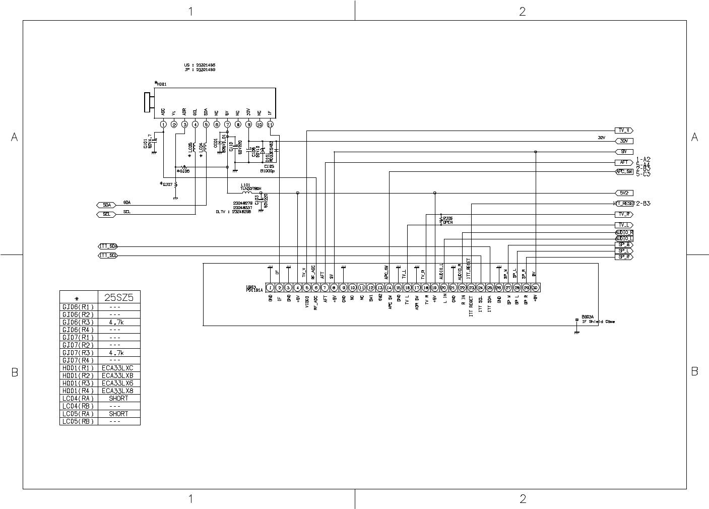
25CSZ5TR/25SZ5ST/25SZ5VX MAIN (TUNER)
SHEET-1/9
(1/11)

|
|
|
|
0V |
|
|
|
|
|
0V |
|
2.0Vp-p |
3.8V |
|
4.0V |
|
|
|
|
|
|
||
|
|
|
4.0V |
|
|
|
3.8V |
|
5.2V |
|
|
|
4.0V |
|
5.2V |
|
|
|
4.5V |
|
5.2V |
|
|
|
4.0V |
|
5.2V |
|
|
|
|
|
|
|
|
|
3.8V |
|
5.2V |
|
|
|
9.0V |
|
5.2V |
|
|
|
3.8V |
|
5.2V |
|
|
|
|
9.0V |
5.2V |
|
|
|
|
|
|
|
|
|
|
5.2V |
|
|
|
|
|
4.0V |
5.2V |
|
|
|
|
|
|
|
|
|
|
5.2V |
5.2V |
|
|
|
|
|
|
|
|
|
0V |
|
5.2V |
4.5V |
|
|
|
|
0V |
|
9.0V |
|
|
|
9.0V |
|
3.9V |
|
|
|
4.0V |
|
|
|
|
|
0V |
|
|
|
|
|
3.4V |
|
|
|
3.5V |
|
|
|
|
|
3.3V |
|
|
9.0V |
|
|
|
4.0V |
|
|
|
|
|
|
|
|
|
|
3.3V |
|
|
3.4V |
|
|
|
|
|
|
|
|
3.3V |
|
|
|
|
|
|
|
|
0V |
|
|
|
|
|
0V |
|
|
|
|
|
0V |
0V |
|
|
|
|
0V |
|
|
|
|
|
|
0V |
25CSZ5TR/25SZ5ST/25SZ5VX MAIN (AV SW)
SHEET-2/9
(2/11)
 Loading...