

DESCRIPTION
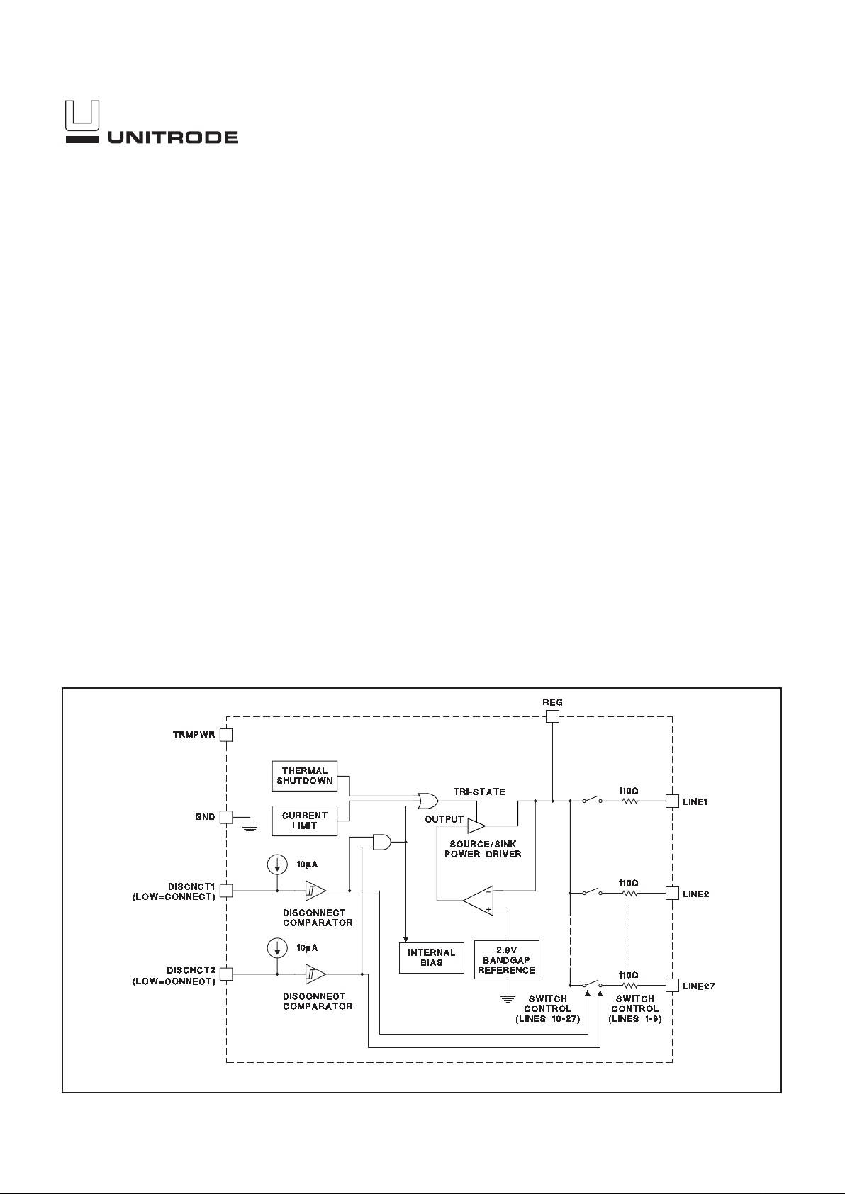
The UCC5622 provides 27 lines of active termination for a SCSI (Small
Computer Systems Interface) parallel bus. The SCSI standard recommends active termination at both ends of the cable.
The UCC5622 is ideal for high performance 5V SCSI systems. During disconnect the supply current is typically only 100µA, which makes the IC attractive for lower powered systems.
The UCC5622 features a split disconnect allowing the user to control termination lines 10 to 27 with disconnect one, DISCNCT1, and control terminiation lines 1 to 9 with disconnect two, DISCNCT2.
The UCC5622 is designed with a low channel capacitance of 2.5pF, which
eliminates effects on signal integrity from disconnected terminators at interim points on the bus.
The power amplifier output stage allows the UCC5622 to source full termination current and sink active negation current when all termination lines
are actively negated.
The UCC5622, as with all Unitrode terminators, is completely hot pluggable and appears as high impedance at the teminating channels with
V
TRMPWR
= 0V or open.
Internal circuit trimming is utilized, first to trim the 110Ω impedance, and
then most importantly, to trim the output current as close to the maximum
SCSI-3 specification as possible, which maximizes noise margin in FAST20 SCSI operation.
(continued)
UCC5622
27 - Line SCSI Terminator With Split Disconnect
BLOCK DIAGRAM
FEATURES
• Complies with SCSI, SCSI-2, SCSI-3,
SPI and FAST-20 (Ultra) Standards
• 2.5pF Channel Capacitance During
Disconnect
• 100µA Supply Current in Disconnect
Mode
• 4V To 7V Operation
• 110Ω Termination
• Completely Meets SCSI Hot Plugging
• –900mA Sourcing Current for
Termination
• +500mA Sinking Current for Active
Negation
• Logic Command Disconnects all
Termination Lines
• Split Disconnect Controls Lines 1 to 9
and 10 to 27 Separately
• Trimmed Impedance to 5%
• Current Limit and Thermal Shutdown
Protection
10/98
UDG-96113
Circuit Design Patented
2
UCC5622
Other features include thermal shutdown and current limit.
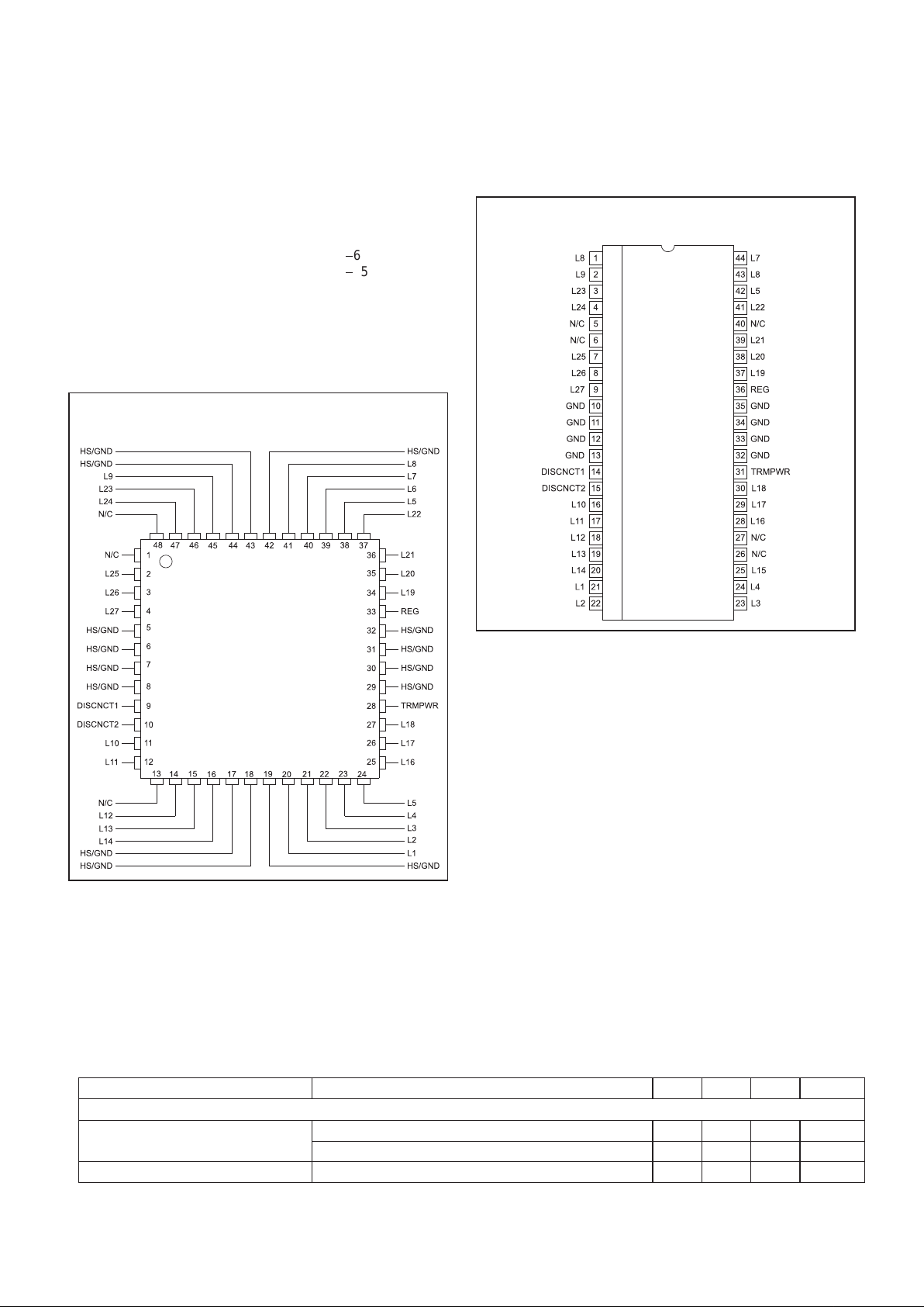
This device is offered in low thermal resistance versions
of the industry standard 44 pin wide body QSOP (MWP)
and 48 pin LQFP (FQP). Consult QSOP-44 and LQFP-48
Packaging Diagram for exact dimensions.
DESCRIPTION (cont.)
CONNECTION DIAGRAM
SSOP-44 (Top View)
MWP Package
LQFP-48 (Top View)
MWP Package
ABSOLUTE MAXIMUM RATINGS
TRMPWR Voltage................................+7V
Signal Line Voltage ..........................0Vto+7V
Regulator Output Current..........................1.5A
Storage Temperature ...................-65°C to +150°C
Junction Temperature...................-55°C to +150°C
Lead Temperature (Soldering, 10 Sec.).............+300°C
Currents are positive into, negative out of the specified terminal. Consult Packaging Section of Databook for thermal limitations and considerations of packages.
ELECTRICAL CHARACTERISTICS Unless otherwise stated, these specifications apply for T
A
= 0°C to 70°C,
TRMPWR = 4.75V, DISCNCT1 = DSCNCT2 = 0V, TA=TJ.
PARAMETER TEST CONDITIONS MIN TYP MAX UNITS
Supply Current Section
TRMPWR Supply Current All Termination Lines = Open 1 2 mA
All Termination Lines = 0.2V 630 650 mA
Power Down Mode DISCNCT1 = DSCNCT2 = TRMPWR 100 200 µA

3
UCC5622
ELECTRICAL CHARACTERISTICS
Unless otherwise stated, these specifications apply for TA= 0°C to 70°C,
TRMPWR = 4.75V, DISCNCT1 = DSCNCT2 = 0V, TA=TJ.
PARAMETER TEST CONDITIONS MIN TYP MAX UNITS
Output Section (Termination Lines)
Termination Impedance (Note 3) 104.5 110 115.5 Ω
Output High Voltage (Note 1) 2.6 2.8 3.0 V
Max Output Current V
LINE
= 0.2V, TJ =25⊃C
-
22.1-23.3-24 mA
V
LINE
= 0.2V
-
20.7-23.3-24 mA
V
LINE
= 0.2V, TRMPWR = 4V, TJ=25°C (Note 1)
-
21
-
23
-
24 mA
V
LINE
= 0.2V, TRMPWR = 4V (Note 1)
-
20
-
23
-
24 mA
V
LINE
= 0.5V
-
22.4 mA
Output Leakage DISCNCT1 = DISCNCT2 = 2.4V, TRMPWR = 0V to
5.25V
10 400 nA
Output Capacitance DISCNCT1 = DISCNCT2 = 2.4V (Note 2) 2.5 4 pF
Regulator Section
Regulator Output Voltage 2.6 2.8 3.0 V
Drop Out Voltage All Termination Lines = 0.2V 0.4 0.8 V
Short Circuit Current V
REG
=0V
-
650-900 –1300 mA
Sinking Current Capability V
REG
= 3.5V 300 500 900 mA
Thermal Shutdown 170 °C
Thermal Shutdown Hysteresis 10 °C
Disconnect Section
Disconnect Threshold DISCNCT1 Controls Lines 10 to 27 0.8 1.5 2.0 V
Input Current DISCNCT1 DISCNCT1 = 0V –10 –30 µA
Disconnect Threshold DISCNCT2 Controls Lines 1 to 9 0.8 1.5 2 V
Input Current DISCNCT2 DISCNCT2 = 0V –10 –30 µA
Note 1:Measuring each termination line while other 26 are low (0.2V).
Note 2:Guaranteed by design. Not 100% tested in production.
Note 3: Tested by measuring I
OUT
with V
OUT
= 0.2V and V
OUT
with no load, then calculate:
Z
VNL V
IatV
OUT
OUT
=
−
.. ..02
20
PIN DESCRIPTIONS
DISCNCT1: Disconnect one controls termination lines
10 – 27. Taking this pin high or leaving it open causes
termination lines 10 - 27 to become high impedence, taking this pin low allows the channels to provide normal termination.
DISCNCT2: Disconnect two controls termination lines
1 – 9. Taking this pin high or leaving it open causes
termination lines1-9tobecome high impedence. Taking
this pin low allows the channels to provide normal
terminiation. Taking both disconnect pins high or leaving
them open will put the chip in to sleep mode where it will
be in low-power mode.
GND: Ground reference for the IC.
L1 – L27: 110Ω termination channels.
REG: Output of the internal 2.7V regulator.
TRMPWR: Power for the IC.
4
UCC5622
UNITRODE CORPORATION
7 CONTINENTAL BLVD·MERRIMACK, NH 03054
TEL (603) 424-2410·FAX(603) 424-3460
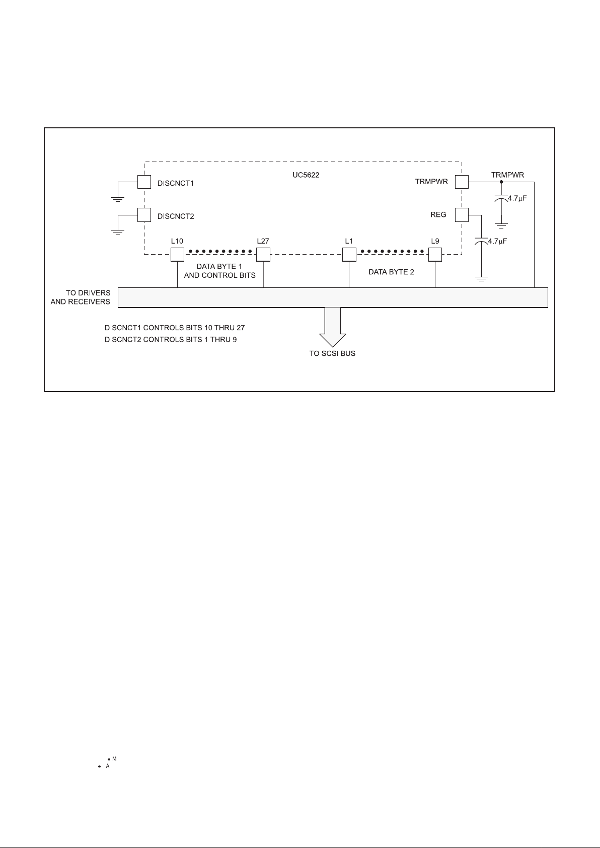
Figure 1. Typical Wide SCSI Bus Configuration Using the UCC5622
UDG-98172

IMPORTANT NOTICE
T exas Instruments and its subsidiaries (TI) reserve the right to make changes to their products or to discontinue
any product or service without notice, and advise customers to obtain the latest version of relevant information
to verify, before placing orders, that information being relied on is current and complete. All products are sold
subject to the terms and conditions of sale supplied at the time of order acknowledgement, including those
pertaining to warranty, patent infringement, and limitation of liability.
TI warrants performance of its semiconductor products to the specifications applicable at the time of sale in
accordance with TI’s standard warranty. Testing and other quality control techniques are utilized to the extent
TI deems necessary to support this warranty. Specific testing of all parameters of each device is not necessarily
performed, except those mandated by government requirements.
CERT AIN APPLICATIONS USING SEMICONDUCTOR PRODUCTS MAY INVOLVE POTENTIAL RISKS OF
DEATH, PERSONAL INJURY, OR SEVERE PROPERTY OR ENVIRONMENTAL DAMAGE (“CRITICAL
APPLICATIONS”). TI SEMICONDUCTOR PRODUCTS ARE NOT DESIGNED, AUTHORIZED, OR
WARRANTED TO BE SUITABLE FOR USE IN LIFE-SUPPORT DEVICES OR SYSTEMS OR OTHER
CRITICAL APPLICATIONS. INCLUSION OF TI PRODUCTS IN SUCH APPLICA TIONS IS UNDERSTOOD T O
BE FULLY AT THE CUSTOMER’S RISK.
In order to minimize risks associated with the customer’s applications, adequate design and operating
safeguards must be provided by the customer to minimize inherent or procedural hazards.
TI assumes no liability for applications assistance or customer product design. TI does not warrant or represent
that any license, either express or implied, is granted under any patent right, copyright, mask work right, or other
intellectual property right of TI covering or relating to any combination, machine, or process in which such
semiconductor products or services might be or are used. TI’s publication of information regarding any third
party’s products or services does not constitute TI’s approval, warranty or endorsement thereof.
Copyright 1999, Texas Instruments Incorporated
 Loading...