

Texas Instruments UCC39151PWPTR, UCC39151PWP, UCC39151N, UCC39151DPTR, UCC39151DP Datasheet
02/99
FEATURES
• Integrated 0.15Ω Power MOSFET
• 7V to 15V Operation
• Digital Programmable Current Limit
from 0A to 3A
• Programmable ON Time
• Programmable Start Delay
• Fixed 2% Duty Cycle
• Thermal Shutdown
• Fault Output Indicator
• Maximum Output Current can be set
to 1A above the Programmed Fault
Level or to a full 4A
• Power SOIC and TSSOP, Low
Thermal Resistance Packaging
DESCRIPTION
The UCC39151 Programmable Hot Swap Power Manager provides complete power management, hot swap capability, and circuit breaker functions. The only external component required to operate the device, other
than power supply bypassing, is the fault timing capacitor, C
T
. All control
and housekeeping functions are integrated, and externally programmable.
These include the fault current level, maximum output sourcing current,
maximum fault time, and startup delay. In the event of a constant fault, the
Internal fixed 2% duty cycle ratio limits average output power.
The internal 4 bit DAC allows programming of the fault level current from
0A to 3A with 0.25A resolution. The IMAX control pin sets the maximum
sourcing current to 1A above the trip level or to a full 4A of output current
for fast output capacitor charging.
When the output current is below the fault level, the output MOSFET is
switched ON with a nominal ON resistance of 0.15Ω. When the output current exceeds the fault level, but is less than the maximum sourcing level,
the output remains switched ON, but the fault timer starts, charging CT.
Once CT charges to a preset threshold, the switch is turned OFF, and remains OFF for 50 times the programmed fault time. When the output current reaches the maximum sourcing level, the MOSFET transitions from a
switch to a constant current source.
(continued)
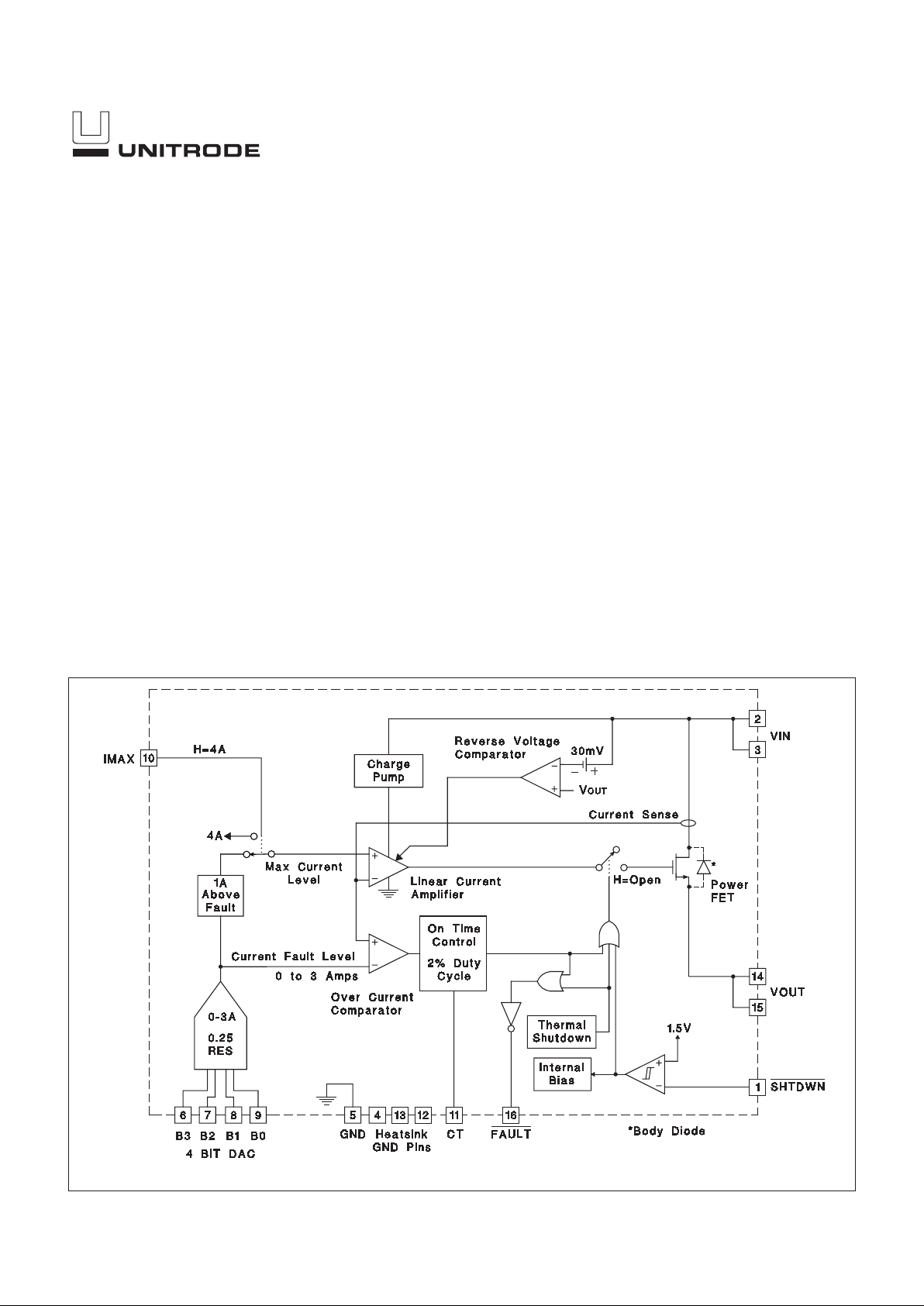
BLOCK DIAGRAM
UCC39151
15V Programmable Hot Swap Power Manager
UDG-94136-3
Note: Pin numbers refer to DIL-16 and SOIC-16 packages.
2
UCC39151
ABSOLUTE MAXIMUM RATINGS
VIN. . . . . . . . . . . . . . . . . . . . . . . . . . . . . . . . . . . . . . +15.5 Volts
VOUT VIN. . . . . . . . . . . . . . . . . . . . . . . . . . . . . . . . . . . . .0.3V
FAULT Sink Current. . . . . . . . . . . . . . . . . . . . . . . . . . . . . 50mA
FAULT Voltage . . . . . . . . . . . . . . . . . . . . . . . . . . . . . 0.3 to 8V
Output Current . . . . . . . . . . . . . . . . . . . . . . . . . . . . Self Limiting
TTL Input Voltage . . . . . . . . . . . . . . . . . . . . . . . . . . 0.3 to V
IN
Storage Temperature . . . . . . . . . . . . . . . . . . . 65 C to +150 C
Junction Temperature. . . . . . . . . . . . . . . . . . . 55 C to +150 C
Lead Temperature (Soldering, 10 sec.). . . . . . . . . . . . . +300 C
Currents are positive into, negative out of the specified terminal. Consult Packaging Section of Databook for thermal limitations and considerations of packages.
FAULT16
15
14
13
12
11
10
9
1
2
3
4
5
6
7
8
VOUT
VOUT
GND*
GND*
CT
IMAX
B0
SHTDWN
VIN
VIN
GND*
EGND*
B3
B2
B1
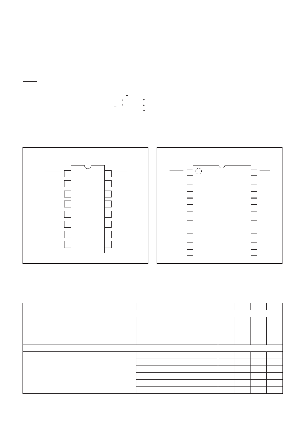
CONNECTION DIAGRAMS
*Pin 5 serves as lowest impedance to the electrical ground;
Pins 4, 12, and 13 serve as heat sink/ground. These pins
should be connected to large etch areas to help dissipate heat.
For N Package, pins 4, 12, and 13 are N/C.
DESCRIPTION (cont.)
The UCC39151 can be put into sleep mode, drawing
only 20mA of supply current. Other features include an
open drain Fault Output Indicator, Thermal Shutdown,
Undervoltage Lockout, 7V to 15V operation, and low
thermal resistance SOIC and TSSOP Power Packages.
B3
N/C
N/C
GND*
GND*
FAULT
VIN
EGND*
GND*
GND*
VIN
N/C
GND*
SHTDWN
GND*
B2
GND*
GND*
CT
12
11
10
9
8
7
6
5
4
3
2
1
13
14
15
16
17
18
19
20
21
22
23
24
IMAX
VOUT
VOUT
B1 B0
*Pin 9 serves as lowest impedance to the electrical ground;
other GND pins serve as heat sink/ground. These pins should
be connected to large etch areas to help dissipate heat.
DIL-16, SOIC-16 (Top View)
N, DP Package
PWP-24 (Top View)
TSSOP Package
ELECTRICAL CHARACTERISTICS Unless otherwise stated, these specifications apply for TA = 0°C to 70°C for the
UCC39151, VIN = 12V, IMAX = 0.4V, SHTDWN = 2.4V, TA= TJ.
PARAMETER TEST CONDITIONS MIN TYP MAX UNITS
Supply Section
Voltage Input Range 7.0 15.0 V
Supply Current 1.0 2.0 mA
Sleep Mode Current SHTDWN
= 0.2V, No load 100 150 µA
Output Leakage SHTDWN
= 0.2V 20 mA
Output Section
Voltage Drop I
OUT
= 1A (10V to 12V) 0.15 0.3 V
I
OUT
= 2A (10V to 12V) 0.3 0.6 V
I
OUT
= 3A (10V to 12V) 0.45 0.9 V
I
OUT
= 1A, VIN = 7V and 15V 0.2 0.4 V
I
OUT
= 2A, VIN = 7V and 15V 0.4 0.8 V
IOUT = 3A, VIN = 7V, 12V Max. 0.6 1.2 V

3
UCC39151
ELECTRICAL CHARACTERISTICS
Unless otherwise stated, these specifications apply for TA = 0°C to 70°C for the
UCC39151, VIN = 12V, IMAX = 0.4V, SHTDWN = 2.4V, TA= TJ.
PARAMETER TEST CONDITIONS MIN TYP MAX UNITS
Output Section (continued)
Initial Startup Time (Note 2) 100 µs
Short Circuit Response (Note 2) 100 ns
DAC Section
Trip Current Code = 0000-0011 (Device Off)
Code = 0100 0.07 0.25 0.45 A
Code = 0101 0.32 0.50 0.7 A
Code = 0110 0.50 0.75 0.98 A
Code = 0111 0.75 1.00 1.3 A
Code = 1000 1.0 1.25 1.6 A
Code = 1001 1.25 1.50 1.85 A
Code = 1010 1.5 1.75 2.15 A
Code = 1011 1.70 2.00 2.4 A
Code = 1100 1.90 2.25 2.7 A
Code = 1101 2.1 2.50 2.95 A
Code = 1110 2.30 2.75 3.25 A
Code = 1111 2.50 3.0 3.5 A
Max Output Current Over Trip (Current Source
Mode)
Code = 0100 to 1111, I
MAX
= 0V 0.35 1.0 1.65 A
Max Output Current (Current Source Mode) Code = 0100 to 1111, I
MAX
= 2.4V 3.0 4.0 5.2 A
Fault Output Section
CT Charge Current V
CT
= 1.0V 83 –62 47 µA
CT Discharge Current VCT= 1.0V 0.8 1.2 1.8 µA
Output Duty Cycle V
OUT
= 0V 1.0 1.9 3.3 %
CT Fault Threshold 1.2 1.5 1.7 V
CT Reset Threshold 0.4 0.5 0.6 V
Shutdown Section
Shutdown Threshold 1.1 1.5 1.9 V
Shutdown Hysteresis 150 mV
Input Current 100 500 nA
Open Drain Output Section
High Level Output Current FAULT
= 5V 250 µA
Low Level Output Voltage I
OUT
= 5mA 0.2 0.8 V
TTL Input DC Characteristics Section
TTL Input Voltage High 2.0 V
TTL Input Voltage Low 0.8 V
TTL Input High Current V
IH
= 2.4V 3 10 µA
TTL Input Low Current VIL= 0.4V 1 µA
Note 1: All voltages are with respect to Ground. Current is positive into and negative out of the specified terminal.
Note 2: Guaranteed by design. Not 100% tested in production.

4
UCC39151
PIN DESCRIPTIONS
B0, B1, B2, B3: These pins provide digital input to the
DAC, which sets the fault current threshold. They can be
used to provide a digital soft-start and adaptive current
limiting.
CT: A capacitor connected to ground sets the maximum
fault time. The maximum fault time must be more than
the time required to charge the external capacitance in
one cycle. The maximum fault time is defined as:
TC
FAULT T
=••16 1 10
3
.
.
Once the fault time is reached the output will shutdown
for a time given by:
TC
SD T
=••833 10
3
,
this equates to a 1.9% duty cycle.
FAULT: Open drain output, which pulls low upon any
fault or interrupt condition, Fault, or Thermal Shutdown.
IMAX: When this pin is set to a logic low, the maximum
sourcing current will always be 1A above the programmed fault level. When set to a logic high, the maximum sourcing current will be a constant 4A for
applications which require fast charging of load capacitance.
SHTDWN
: When this pin is brought to a logic low, the IC
is put into a sleep mode drawing typically less than
100µAofICC(with V
OUT
unloaded). The input threshold
is hysteretic, allowing the user to program a startup delay
with an external RC circuit.
VIN: Input voltage to the UCC39151. The recommended
voltage range is 7V to 15V. Both VIN pins should be connected together and connected to power source.
VOUT: Output voltage from the UCC39151. Both VOUT
pins should be connected together and connected to the
load. When switched:
()
VV I
OUT IN OUT
≈− •015. Ω
VOUT must not exceed VIN by more than 0.3V.
SHTDWN
14
15
10
1
2
16
11
VOUT
CT
+5V
VIN
FAULT
B0
GND
R
L
C
IN
LED
513124
GNDGNDGND
C
OUT
C
SD
R
SD
V
IN
S6
6789
V
IN
S4S3S2 S5
B1 B2 B3 IMAX
S1
C
T
R1
3VIN
V
IN
HEATSINK GROUND PINS
UCC39151
DIP SWITCH
APPLICATIONS INFORMATION
Figure 1. Evaluation circuit.
UDG-98176

5
UCC39151
APPLICATION INFORMATION (cont.)
Figure 2. Load current, timing capacitor voltage, and output voltage of the UCC39151 under fault conditions.
Estimating Maximum Load Capacitance
For hot swap applications, the rate at which the total
output capacitance can be charged depends on the
maximum output current available and the nature of the
load. For a constant-current, current-limited application,
the output will come up if the load asks for less than the
maximum available short-circuit current.
To guarantee recovery of a duty-cycle from a shortcircuited load condition, there is a maximum total output
capacitance which can be charged for a given unit ON
time (Fault time). The design value of ON or Fault time
can be adjusted by changing the timing capacitor C
T
.
For worst-case constant-current load of value just less
than the trip limit; C
OUT(max)
can be estimated from:
()
CII
C
V
OUT MAX LOAD
T
OUT
(max)
.
≈− •
••
16 1 10
3
Where V
OUT
is the output voltage.
For a resistive load of value RI, the value of C
OUT(max)
can be estimated from:
C
C
Rn
V
IR
OUT
T
L
OUT
MAX L
(max)
.≈••
•
−
•
16 1 10
1
1
3
Long C
T
times must consider the maximum temperature. Thermal shutdown protection may be the limiting
Fault time.
UDG-94138
UNITRODE CORPORATION
7 CONTINENTAL BLVD ( MERRIMACK, NH 03054
TEL (603) 424-2410 ( FAX (603) 424-3460
Although the UCC39151 is designed to provide system
protection for all fault conditions, all integrated circuits
can ultimately fail short. For this reason, if the
UCC39151 is intended for use in safety critical applications where UL or some other safety rating is required, a
redundant safety device such as a fuse should be placed
in series with the device. The UCC39151 will prevent the
fuse from blowing for virtually all fault conditions, increasing system reliability and reducing maintenance
cost, in addition to providing the hot swap benefits of the
device.
SAFETY RECOMMENDATIONS

IMPORTANT NOTICE
T exas Instruments and its subsidiaries (TI) reserve the right to make changes to their products or to discontinue
any product or service without notice, and advise customers to obtain the latest version of relevant information
to verify, before placing orders, that information being relied on is current and complete. All products are sold
subject to the terms and conditions of sale supplied at the time of order acknowledgement, including those
pertaining to warranty, patent infringement, and limitation of liability.
TI warrants performance of its semiconductor products to the specifications applicable at the time of sale in
accordance with TI’s standard warranty. Testing and other quality control techniques are utilized to the extent
TI deems necessary to support this warranty. Specific testing of all parameters of each device is not necessarily
performed, except those mandated by government requirements.
CERT AIN APPLICATIONS USING SEMICONDUCTOR PRODUCTS MAY INVOLVE POTENTIAL RISKS OF
DEATH, PERSONAL INJURY, OR SEVERE PROPERTY OR ENVIRONMENTAL DAMAGE (“CRITICAL
APPLICATIONS”). TI SEMICONDUCTOR PRODUCTS ARE NOT DESIGNED, AUTHORIZED, OR
WARRANTED TO BE SUITABLE FOR USE IN LIFE-SUPPORT DEVICES OR SYSTEMS OR OTHER
CRITICAL APPLICATIONS. INCLUSION OF TI PRODUCTS IN SUCH APPLICA TIONS IS UNDERSTOOD T O
BE FULLY AT THE CUSTOMER’S RISK.
In order to minimize risks associated with the customer’s applications, adequate design and operating
safeguards must be provided by the customer to minimize inherent or procedural hazards.
TI assumes no liability for applications assistance or customer product design. TI does not warrant or represent
that any license, either express or implied, is granted under any patent right, copyright, mask work right, or other
intellectual property right of TI covering or relating to any combination, machine, or process in which such
semiconductor products or services might be or are used. TI’s publication of information regarding any third
party’s products or services does not constitute TI’s approval, warranty or endorsement thereof.
Copyright 1999, Texas Instruments Incorporated
 Loading...