

Page 1

www.ti.com
Table of Contents
Functional Safety Information
Safety Manual for TMS320F28002x
ABSTRACT
This document is a safety manual for the Texas Instruments TMS320F28002x safety critical real time
microcontroller product family. The product family utilizes a common safety architecture that is implemented
in multiple application-focused products.
Table of Contents
1 Introduction.............................................................................................................................................................................3
2 TMS320F28002x Product Safety Capability and Constraints............................................................................................. 4
3 TI Development Process for Management of Systematic Faults....................................................................................... 4
3.1 TI New-Product Development Process.............................................................................................................................. 4
3.2 TI Safety Development Process.........................................................................................................................................5
4 TMS320F28002x Product Overview...................................................................................................................................... 7
4.1 C2000 Architecture and Product Overview........................................................................................................................ 7
4.2 Functional Safety Concept................................................................................................................................................. 8
4.3 C2000 Safety Diagnostics Libraries................................................................................................................................. 16
4.4 TMS320F28002x MCU Safety Implementation................................................................................................................16
5 Brief Description of Safety Elements..................................................................................................................................17
5.1 TMS320F28002x MCU Infrastructure Components.........................................................................................................18
5.2 Processing Elements....................................................................................................................................................... 21
5.3 Memory (Flash, SRAM and ROM)................................................................................................................................... 22
5.4 On-Chip Communication Including Bus-Arbitration..........................................................................................................24
5.5 Digital I/O......................................................................................................................................................................... 27
5.6 Analog I/O........................................................................................................................................................................ 29
5.7 Data Transmission........................................................................................................................................................... 30
6 Brief Description of Diagnostics......................................................................................................................................... 34
6.1 TMS320F28002x MCU Infrastructure Components.........................................................................................................34
6.2 Processing Elements....................................................................................................................................................... 39
6.3 Memory (Flash, SRAM and ROM)................................................................................................................................... 41
6.4 On-Chip Communication Including Bus-Arbitration..........................................................................................................44
6.5 Digital I/O......................................................................................................................................................................... 46
6.6 Analog I/O........................................................................................................................................................................ 52
6.7 Data Transmission........................................................................................................................................................... 55
7 References............................................................................................................................................................................ 61
A Safety Architecture Configurations....................................................................................................................................62
A.1 Safety Architecture Configurations.................................................................................................................................. 62
B Distributed Developments...................................................................................................................................................66
B.1 How the Functional Safety Lifecycle Applies to Functional Safety-Compliant Products..................................................66
B.2 Activities Performed by Texas Instruments......................................................................................................................66
B.3 Information Provided........................................................................................................................................................67
C Summary of Safety Features and Diagnostics..................................................................................................................68
C.1 Summary of Safety Features and Diagnostics................................................................................................................ 68
D Glossary................................................................................................................................................................................89
D.1 Glossary...........................................................................................................................................................................89
List of Figures
Figure 3-1. TI New-Product Development Process..................................................................................................................... 5
Figure 4-1. Functional Block Diagram of TMS320F28002x MCU................................................................................................7
Figure 4-2. Definition of the TMS320F28002x MCU Used in a Compliant Item.......................................................................... 8
Figure 4-3. TMS320F28002x MCU With Safety Features........................................................................................................... 9
Figure 4-4. Relationship Between DTI, Fault Reaction Time and FTTI..................................................................................... 10
SPRUIT5 – APRIL 2021
Submit Document Feedback
Copyright © 2021 Texas Instruments Incorporated
Safety Manual for TMS320F28002x 1
Page 2

Trademarks
Figure 4-5. TMS320F28002x MCU Safe State Definition.......................................................................................................... 11
Figure 4-6. TMS320F28002x MCU Device Operating States....................................................................................................12
Figure 4-7. TMS320F28002x MCU CPU Start-Up Sequence................................................................................................... 13
Figure 4-8. Fault Response Severity......................................................................................................................................... 13
Figure 4-9. Safety Concept Implementation.............................................................................................................................. 17
Figure 5-1. Generic Hardware of a System............................................................................................................................... 18
Figure 6-1. Stack Overflow Monitoring...................................................................................................................................... 40
Figure 6-2. ePWM Fault Detection Using X-BAR...................................................................................................................... 46
Figure 6-3. Monitoring of ePWM by ADC.................................................................................................................................. 49
Figure 6-4. HRCAP Calibration..................................................................................................................................................51
Figure 6-5. QMA Module Block Diagram................................................................................................................................... 52
Figure 6-6. DAC to ADC Loopback............................................................................................................................................53
Figure 6-7. ADC Open-Shorts Detection Circuit........................................................................................................................ 54
www.ti.com
List of Tables
Table 1-1. Products Supported by This Safety Manual................................................................................................................3
Table 3-1. Functional Safety Activities Overlaid on top of TI's Standard Development Process................................................. 6
Table 4-1. F28002x Diagnostic Library details...........................................................................................................................16
Table 6-1. ADC Open-Shorts Detection Circuit Truth Table.......................................................................................................54
Table A-1. Safety Architecture Configurations........................................................................................................................... 62
Table B-1. Activities Performed by Texas Instruments versus Performed by the customer.......................................................66
Table B-2. Product Functional Safety Documentation............................................................................................................... 67
Table C-1. Summary Table Legend........................................................................................................................................... 68
Table C-2. Summary of Safety Features and Diagnostic...........................................................................................................68
Table D-1. Glossary................................................................................................................................................................... 89
Trademarks
C2000™ is a trademark of Texas Instruments.
All trademarks are the property of their respective owners.
2 Safety Manual for TMS320F28002x SPRUIT5 – APRIL 2021
Copyright © 2021 Texas Instruments Incorporated
Submit Document Feedback
Page 3

www.ti.com
Introduction
1 Introduction
This document is a safety manual for the Texas Instruments TMS320F28002x safety critical real time
microcontroller product family. The product family utilizes a common safety architecture that is implemented
in multiple application focused products.
Product configurations supported by this safety manual include silicon revision A of the following products listed
in Table 1-1 . The device revision can be determined by the REVID field of the device identification registers
outlined in [14].
Table 1-1. Products Supported by This Safety Manual
Orderable Devices Supported Safety Integrity Level
TMS320F280025PN QM
TMS320F280025CPN QM
TMS320F280023PN QM
TMS320F280023CPN QM
TMS320F280025PM QM
TMS320F280025CPM QM
TMS320F280024PM QM
TMS320F280024CPM QM
TMS320F280023PM QM
TMS320F280023CPM QM
TMS320F280022PM QM
TMS320F280025PT QM
TMS320F280025CPT QM
TMS320F280023PT QM
TMS320F280023CPT QM
TMS320F280021PT QM
This Safety Manual provides information needed by system developers to assist in the creation of a safety
critical system using a supported TMS320F28002x MCU. This document contains:
• An overview of the component architecture
• An overview of the development process used to decrease the probability of systematic failures
• An overview of the functional safety architecture for management of random failures
• The details of architecture partitions and implemented functional safety mechanisms
The following information is documented in the Detailed Safety Analysis Report (SAR) for TMS320F28002x
C2000™ Safety Critical Microcontrollers, which is only available under Functional Safety NDA and is not
repeated in this document:
• Failure rates (FIT) of the component
• Fault model used to estimate device failure rates suitable to enable calculation of customized failure rates
• Functional safety metrics of the hardware component for targeted standards (viz. IEC 61508:2010 and ISO
26262:2018)
• Quantitative functional safety analysis (also known as FMEDA, Failure Modes, Effects, and Diagnostics
Analysis) with detail of the different parts of the component, allowing for customized application of functional
safety mechanisms
• Assumptions used in the calculation of functional safety metrics
• Results of assessments of compliance to targeted standards
It is expected that the user of this document should have a general familiarity with the TMS320F28002x product
families. More information can be found at www.ti.com/C2000.
This document is intended to be used in conjunction with the pertinent data sheets, technical reference manuals,
and other documentation for the products being supplied.
SPRUIT5 – APRIL 2021
Submit Document Feedback
Safety Manual for TMS320F28002x 3
Copyright © 2021 Texas Instruments Incorporated
Page 4

TMS320F28002x Product Safety Capability and Constraints
www.ti.com
For information which is beyond the scope of the listed deliverables, contact your TI sales representative or
www.ti.com.
2 TMS320F28002x Product Safety Capability and Constraints
This section summarizes the TMS320F28002x product safety capability. Each TMS320F28002x product:
• Is offered as a functional Safety Element Out Of Context (SEooC)
• Was assessed to have met the relevant systematic capability compliance requirements of IEC 61508:2010
and ISO 26262:2018 and
– Achieves systematic integrity of SIL-3 and ASIL-D
• Contains multiple features to support Freedom From Interference (FFI) for mixed-criticality of safety
requirements assigned to the different sub-elements
• The TMS320F28002x MCUs are Type B devices, as defined in IEC 61508-2:2010
• This device claims no hardware fault tolerance, (for example, no claims of HFT > 0), as defined in IEC
61508:2010
• However, Dual channel with two F28002x devices (common safety card architecture) or one F28002x paired
with second channel integrated in the drive MCU can help to meet HFT=1 topologies with SFF>90%.
– This helps to build system level drive safety in various industrial motor control applications per
IEC61800-5-2 and to meet IEC61508 SIL3, IEC62061 SILCL3, ISO 13849 PLe CAT4 standards.
• For safety components developed according to many safety standards, it is expected that the component
safety manual will provide a list of product safety constraints. For a simple component or more
complex components developed for a single application, this is a reasonable response. However, the
TMS320F28002x MCU product family is both a complex design and is not developed targeting a single,
specific application. Therefore, a single set of product safety constraints cannot govern all viable uses of the
product
Note
This functional safety assessment of this component is not yet complete.
3 TI Development Process for Management of Systematic Faults
For functional safety development, it is necessary to manage both systematic and random faults. Texas
Instruments follows a new-product development process for all of its components which helps to decrease
the probability of systematic failures. This new-product development process is described in Section 3.1.
Components being designed for functional safety applications will additionally follow the requirements of TI's
functional safety development process, which is described in Section 3.2.
3.1 TI New-Product Development Process
Texas Instruments has been developing components for automotive and industrial markets since 1996.
Automotive markets have strong requirements regarding quality management and product reliability. The TI
new-product development process features many elements necessary to manage systematic faults. Additionally,
the documentation and reports for these components can be used to assist with compliance to a wide range
of standards for customer’s end applications including automotive and industrial systems (for example, ISO
26262-4:2018, IEC 61508-2:2010).
This component was developed using TI’s new product development process, which has been certified as
compliant to ISO 9001 / IATF 16949 as assessed by Bureau Veritas (BV).
The standard development process breaks development into phases:
• Assess
• Plan
• Create
• Validate
4 Safety Manual for TMS320F28002x SPRUIT5 – APRIL 2021
Copyright © 2021 Texas Instruments Incorporated
Submit Document Feedback
Page 5
Copyright © 2018, Texas Instruments Incorporated
Assess
Review
Plan
Review
Create
Review
Validate
Review
& Release
To Market
Periodic
Post-Release
Reviews
Phase 1:
Assess
Phase 2:
Plan
Phase 3:
Create
Phase 4:
Validate
Sustain
Identify New
Product
Opportunities
Develop Project
Plan
IC Design &
Layout
Develop Product
Specification
IC Design
Verification
Manage Project Execution and Risks
Develop Test and Validation HW/SW
Develop Datasheet and other
Documentation
Product Support
Product
Monitoring
IC Valdiation
IC Qualification
www.ti.com
Figure 3-1 shows the standard process.
TI Development Process for Management of Systematic Faults
3.2 TI Safety Development Process
The TI functional safety development flow derives from ISO 26262:2018 and IEC 61508:2010 a set of
requirements and methodologies to be applied to semiconductor development. This flow is combined with TI's
standard new product development process to develop Functional Safety-Compliant components. The details
of this functional safety development flow are described in the TI internal specification - Functional Safety
Hardware.
Key elements of the TI functional safety-development flow are as follows:
• Assumptions on system level design, functional safety concept, and requirements based on TI's experience
• Qualitative and quantitative functional safety analysis techniques including analysis of silicon failure modes
• Base FIT rate estimation based on multiple industry standards and TI manufacturing data
• Documentation of functional safety work products during the component development
• Integration of lessons learned through multiple functional safety component developments, functional safety
Table 3-1 lists the functional safety development activities that are overlaid on top of the standard development
flow in Figure 3-1.
For more information about which functional safety lifecycle activities TI performs, see Appendix B.
Figure 3-1. TI New-Product Development Process
with components in functional safety applications
and application of functional safety mechanisms
standard working groups, and the expertise of TI customers
SPRUIT5 – APRIL 2021
Submit Document Feedback
Copyright © 2021 Texas Instruments Incorporated
Safety Manual for TMS320F28002x 5
Page 6

TI Development Process for Management of Systematic Faults www.ti.com
The customer facing work products derived from this Functional Safety-Compliant process are applicable to
many other functional safety standards beyond ISO 26262:2018 and IEC 61508:2010.
Table 3-1. Functional Safety Activities Overlaid on top of TI's Standard Development Process
Assess Plan Create Validate Sustain and End-of-Life
Determine if functional
safety process execution
is required
Nominate a functional
safety manager
End of Phase Audit
Define component target
SIL/ASIL capability
Generate functional safety
plan
Verify the functional safety
plan
Initiate functional safety
case
Analyze target
applications to generate
system level functional
safety assumptions
End of Phase Audit
Develop component
level functional safety
requirements
Include functional safety
requirements in design
specification
Verify the design
specification
Start functional safety
design
Perform qualitative
analysis of design (failure
mode analysis)
Verify the qualitative
analysis
Verify the functional safety
design
Perform quantitative
analysis of design (i.e.
FMEDA)
Verify the quantitative
analysis
Iterate functional safety
design as necessary
End of Phase Audit
Validate functional safety
design in silicon
Characterize the functional
safety design
Qualify the functional
safety design (per AEC-
Q100)
Finalize functional safety
case
Perform assessment of
project
Release functional safety
manual
Release functional safety
analysis report
Release functional safety
report
End of Phase Audit
Document any reported
issues (as needed)
Perform incident reporting
of sustaining operations
(as needed)
Update work products (as
needed)
6 Safety Manual for TMS320F28002x SPRUIT5 – APRIL 2021
Copyright © 2021 Texas Instruments Incorporated
Submit Document Feedback
Page 7
www.ti.com
TMS320F28002x Product Overview
4 TMS320F28002x Product Overview
4.1 C2000 Architecture and Product Overview
The TMS320F28002x devices are powerful 32-bit real time floating-point microcontroller unit (MCU) designed for
advanced closed-loop control applications in automotive and industrial applications.
4.1.1 TMS320F28002x MCU
TMS320F28002x supports C28x as the processing element that boosts system performance for closed loop
control applications. This is a powerful 32-bit real time floating-point microcontroller unit (MCU) that lets system
integrator to access crucial control peripherals, differentiated analog, and nonvolatile memory on a single device.
The C28x CPU is further boosted by the Floating-Point Unit (FPU), Trigonometric Math Unit (TMU), Nonlinear
Proportional Integral Derivative (NLPID) control, Fast Integer Division (FINTDIV) and Cyclic Redundancy
Check (VCRC) accelerators. FPU supports IEEE754 floating point operations. TMU enables fast execution of
algorithms with trigonometric operations common in transforms and torque loop calculations. NLPID enables
fast execution of Nonlinear PID controls. The VCRC engine reduces the time for complex math operations
common in encoded applications. Users may refer to Enhancing the Computational Performance of the C2000™
Microcontroller Family to see how the on-chip hardware math enhancements can be employed to increase the
performance of the MCU in many real-time applications.
The TMS320F28002x supports up to 128KB (64KW) of on-chip flash memory with error correction code (ECC)
and up to 24KB (12KW) of SRAM with parity or ECC.
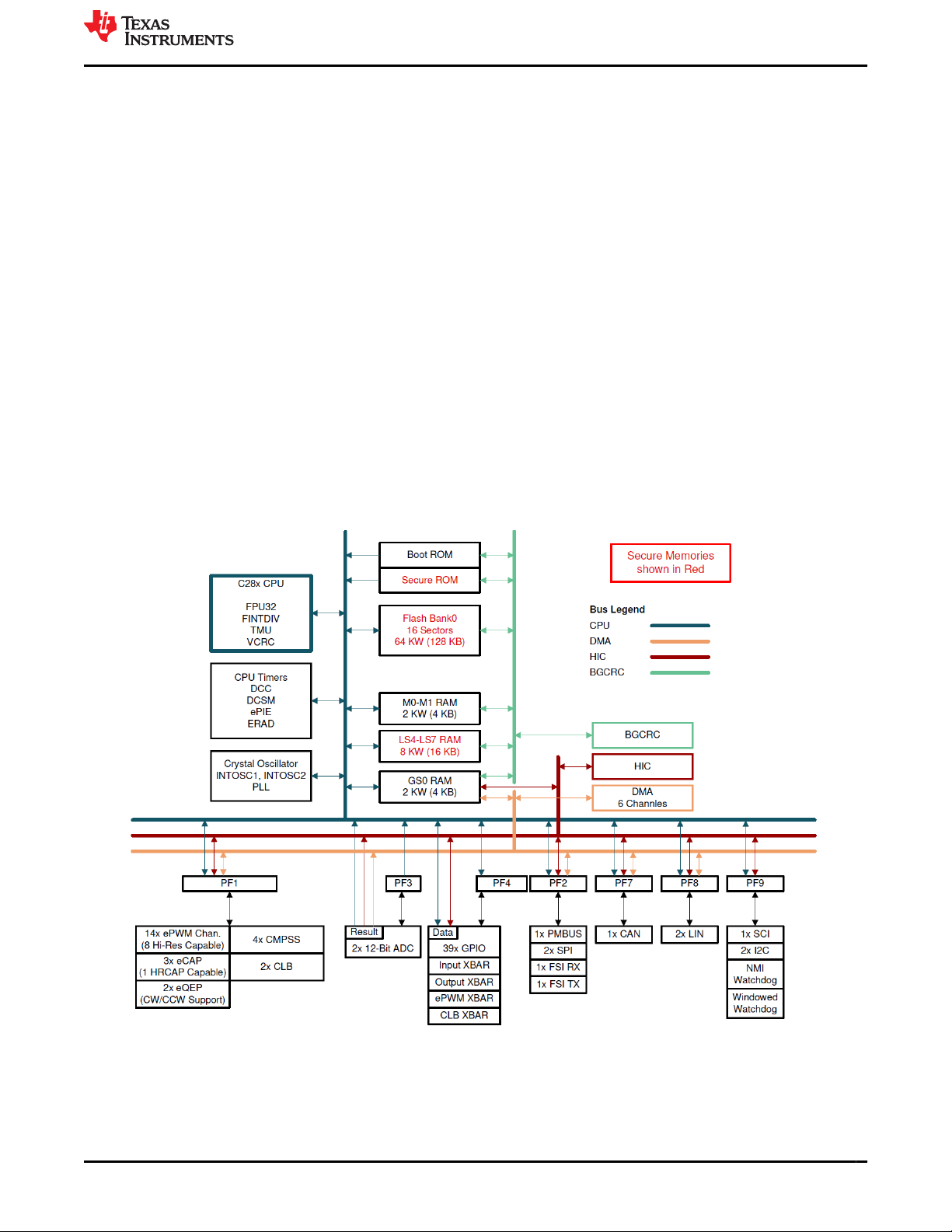
Figure 4-1. Functional Block Diagram of TMS320F28002x MCU
SPRUIT5 – APRIL 2021
Submit Document Feedback
Safety Manual for TMS320F28002x 7
Copyright © 2021 Texas Instruments Incorporated
Page 8
Sensor
Processing
Element
Actuator
S
Remote
Controller
MCU
A
Remote
Controller
S
Remote
Controller
A
Remote
Controller
Sensor
Actuator
Processing Element
TMS320F28002x Product Overview
www.ti.com
Performance analog and control peripherals are also integrated to further enable system consolidation. Two
independent 12-bit ADCs provide precise and efficient management of multiple analog signals, which ultimately
boosts system throughput. The Comparator Subsystem (CMPSS) with windowed comparators allows for
protection of power stages when current limit conditions are exceeded or not met. Other analog and control
peripherals include the Enhanced Pulse Width Modulation (ePWM), Enhanced Capture (eCAP) and Enhanced
Quadrature Encoder Pulse (eQEP).
Peripherals such as Controller Area Network (CAN) modules (ISO11898-1/CAN 2.0B-compliant), Inter-Integrated
Communication (I2C) Bus, Local Interconnect Network (LIN), Serial Communications Interface (SCI), Serial
Peripheral Interface (SPI), Power Management Bus (PMBus) Interface, and Fast Serial Interface (FSI) extend
connectivity of TMS320F28002x MCU. The Fast Serial Interface (FSI) module is a serial communication
peripheral capable of reliable high-speed communication across isolation devices.
The device configurations supported by this safety manual for TMS320F28002x MCUs is outlined in the
TMS320F28002x Real-time Microcontrollers Data Manual. Not all variants are available in all packages or all
temperature grades. To confirm availability, contact your local Texas Instruments sales and marketing.
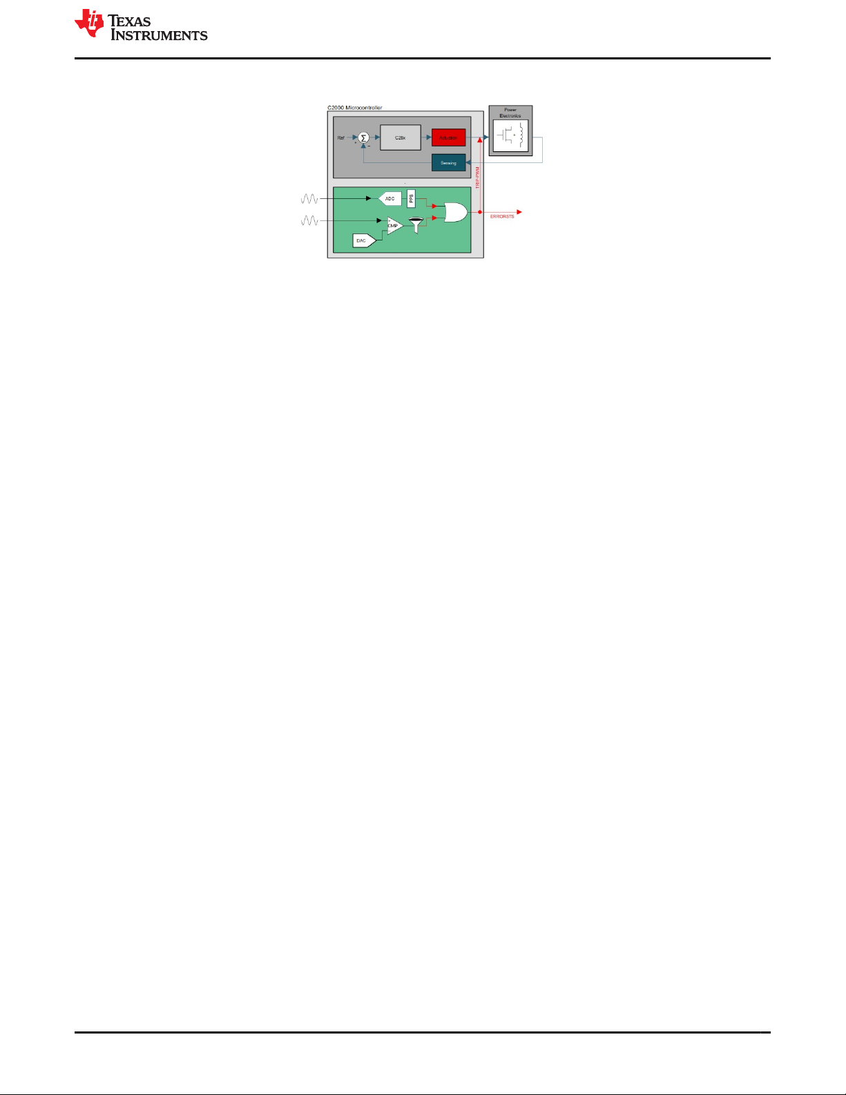
4.2 Functional Safety Concept
To stay as general as possible, the safety concept assumes the MCU playing the role of a processing unit (or
part of it) and connected to remote controller(s) by means of a communication bus as shown in Figure 4-2. The
communication bus is directly or indirectly connected to sensor(s) and actuator(s).
IEC 61508-1:2010 defines a compliant item as any item (for example an element) on which a claim is being
made with respect to the clauses of IEC 61508:2010 series. A system including TMS320F28002x microcontroller
as indicated by Figure 4-2 can be used in a compliant item according to IEC 61508:2010.
Figure 4-2. Definition of the TMS320F28002x MCU Used in a Compliant Item
8 Safety Manual for TMS320F28002x SPRUIT5 – APRIL 2021
Copyright © 2021 Texas Instruments Incorporated
Submit Document Feedback
Page 9
www.ti.com
TMS320F28002x Product Overview
4.2.1 TMS320F28002x MCU Safety Features
Due to the inherent versatility of the device architecture, several software voting based safety configurations are
possible. Some of the safety configurations possible with TMS320F28002x for improving diagnostic coverage
are explained in Table A-1. While implementing these configurations, system integrator needs to consider the
potential common mode failures and address them in an appropriate manner. This may suitably be modified
to adapt to TMS320F28002x requirements based on the availability of processing units. (As stated earlier, the
device claims no hardware fault tolerance, (for example, no claims of HFT > 0), as defined in IEC 61508:2010).
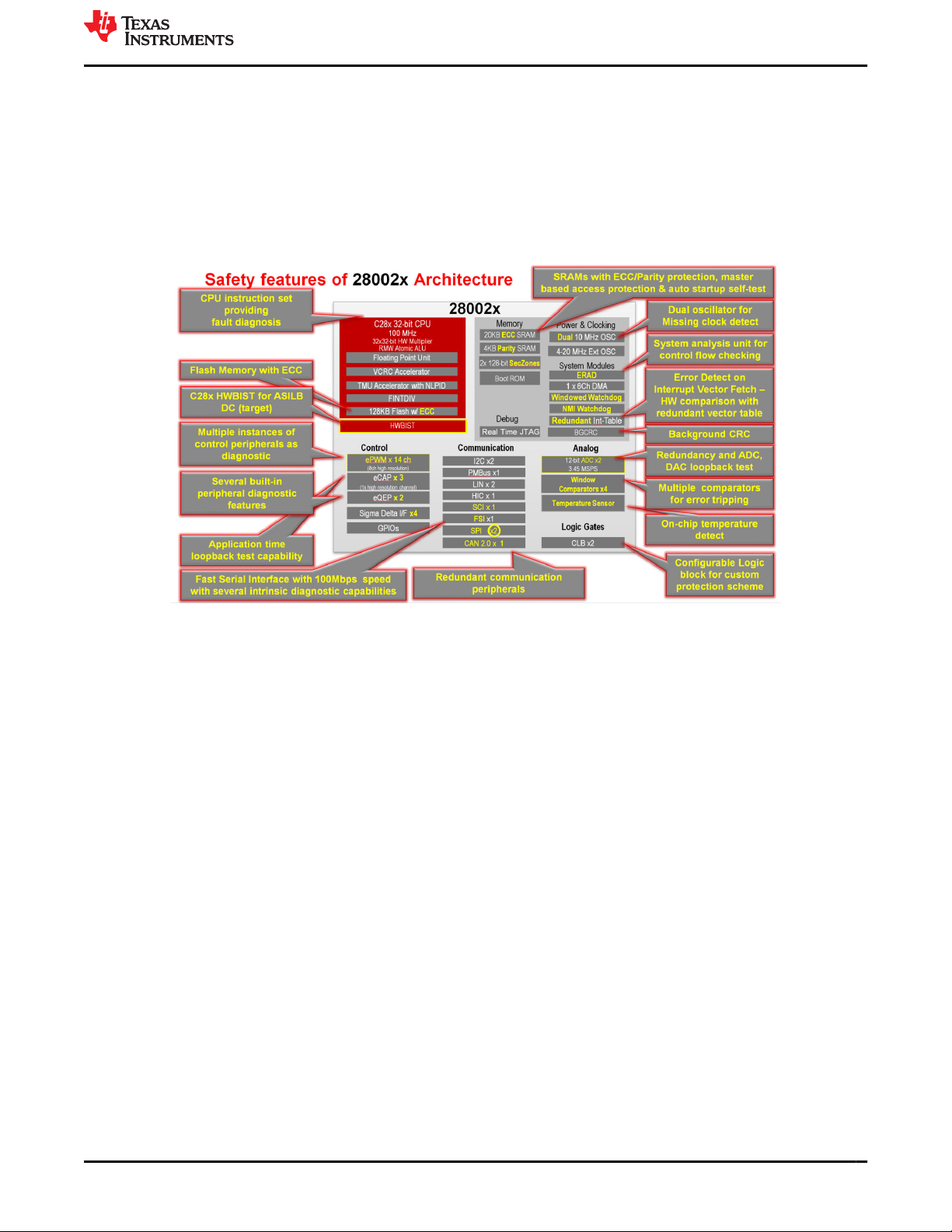
The major safety features of TMS320F28002x are shown in Figure 4-3.
Figure 4-3. TMS320F28002x MCU With Safety Features
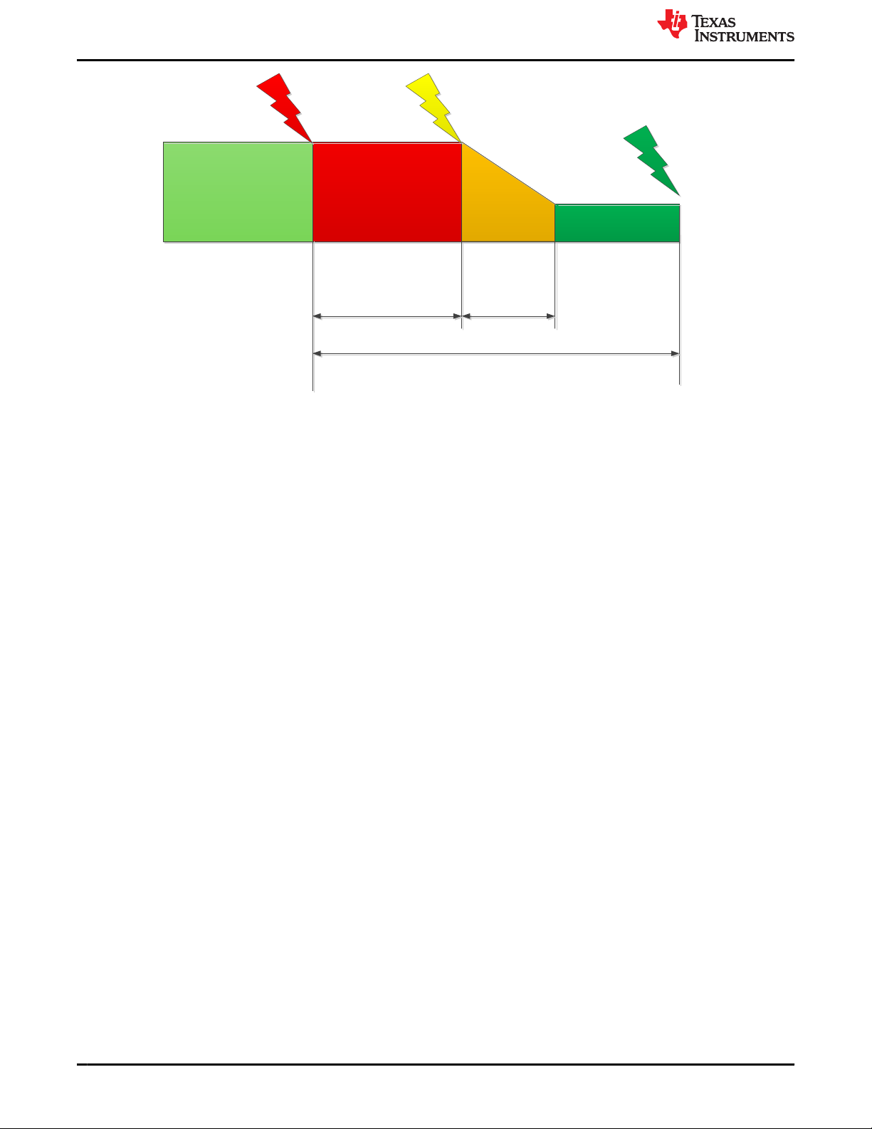
4.2.2 Fault Tolerant Time Interval (FTTI)
Various safety mechanisms in the devices are either always-on (see CPU Handling of Illegal Operation, Illegal
Results and Instruction Trapping and so forth) or executed periodically (see CPU Hardware Built-In Self-Test
(HWBIST) ,VCRC Check of Static Memory Contents, and so forth) by the application software. The time
between the executions of online diagnostic tests by a safety mechanism is termed as Diagnostic test interval
(DTI). Once the fault is detected, depending on the fault reaction of the associated fault (for example, external
system reaction to ERRORSTS pin assertion), the system will enter in the safe-state. The time-span in which a
fault or faults can be present in a system before a hazardous event occurs is called Fault Tolerant Time Interval
(FTTI) as defined in ISO 26262. This is similar to Process Safety Time (PST) defined in IEC 61508. Figure 4-4
illustrates the relationship between DTI, Fault Reaction Time and FTTI.
SPRUIT5 – APRIL 2021
Submit Document Feedback
Safety Manual for TMS320F28002x 9
Copyright © 2021 Texas Instruments Incorporated
Page 10
Fault
Normal Operation Unsafe State
Safe State
Fault
Detection
Hazard
Avoided
T <= DTI
Fault Reaction
Time
FTTI
TMS320F28002x Product Overview
www.ti.com
Figure 4-4. Relationship Between DTI, Fault Reaction Time and FTTI
The frequency and extent of each of the checks in the application should be consistent with the Fault Tolerant
Time Interval (FTTI).The checks should be such that single point faults of the microcontroller should be detected
and responded to, such that the TMS320F28002x MCU enters a safe state within the FTTI budget. The
microcontroller on detection of a fault enters into one of the safe states as illustrated in Figure 4-5. An example
of a diagnostic for single point faults is ECC/Parity for memories.
The proposed functional safety concept, subsequent functional safety features and configurations explained
in this document are for reference purpose only. The system and equipment designer or manufacturer is
responsible to ensure that the end systems (and any Texas Instruments hardware or software components
incorporated in the systems) meet all applicable safety, regulatory and system-level performance requirements.
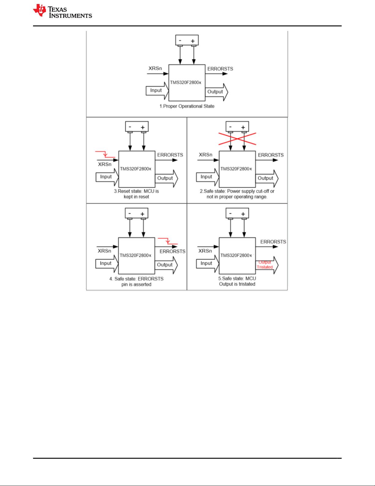
4.2.3 TMS320F28002x MCU Safe State
Referring to Figure 4-5, the safe state of the TMS320F28002x MCU is defined as the one in which:
• TMS320F28002x MCU Reset is asserted
• Power supply to TMS320F28002x MCU is disabled using an external supervisor as a result of a critical
failure. In general, a power supply failure is not considered in detail in this analysis as it is assumed that the
system level functionality exists to manage this condition.
• External system is informed using one of C2000 MCU’s IO pins as a result of a check failure (for example,
ERRORSTS pin is asserted).
• Output of the TMS320F28002x MCU driving the actuator is forced to inactive mode as a result of a check
failure (for example, GPIO pins corresponding to the mission function is tri-stated).
10 Safety Manual for TMS320F28002x SPRUIT5 – APRIL 2021
Copyright © 2021 Texas Instruments Incorporated
Submit Document Feedback
Page 11
www.ti.com
TMS320F28002x Product Overview
SPRUIT5 – APRIL 2021
Submit Document Feedback
Figure 4-5. TMS320F28002x MCU Safe State Definition
Safety Manual for TMS320F28002x 11
Copyright © 2021 Texas Instruments Incorporated
Page 12
Powered
Off
Reset
State
Cold Boot
Warm
Boot
Pre-
Operational
Operational
Power removed
Power applied
Chip Pin Reset
released
Defined Safe State
conditions
CPU1 Reset
released
Device boot phaseCPUSS operation
Safe State
XRSn = 0
TMS320F28002x Product Overview
Figure 4-6. TMS320F28002x MCU Device Operating States
www.ti.com
4.2.4 Operating States
The C2000 MCU products have a common architectural definition of operating states. These operating states
should be observed by the system developer in their software and system level design concepts. The operating
states state machine is shown in Figure 4-6. The operating states can be classified into device boot phase and
CPU Subsystem (CPUSS) operation phase.
The various states of the device operating states state machine are:
• Powered Off - This is the initial operating state of TMS320F28002x MCU. No power is applied to either
core or I/O power supply and the device is non-functional. An external supervisor can perform this action
(power-down the TMS320F28002x MCU) in any of the TMS320F28002x MCU states as response to a
system level fault condition or a fault condition indicated by the TMS320F28002x MCU.
• Reset State – In this state, the device reset is asserted either using the external pins or using any of the
internal sources.
• Safe State – In the Safe state, the device is either not performing any functional operations or an internal fault
condition is indicated using the device I/O pins.
• Cold Boot - In the cold boot state, key analog elements, digital control logic, and debug logic are initialized.
The CPU remains powered but in reset. When the cold boot process is completed, the reset of the CPU is
internally released, leading to the warm boot stage.
• Warm Boot - The CPU begins execution from Boot ROM during the warm boot stage.
• Pre-operational - Transfer of control from boot code to customer code takes place during this phase.
Application specific configurations (for example, clock frequency, peripheral enable, pinmux, and so forth)
are performed in this phase. Boot time self-test/proof-test required to ensure proper device operation is
performed during this phase. See Power-Up Pre-Operational Security Checks for details.
• Operational – This marks the system exiting the pre-operational state and entering the functional state. The
device is capable of supporting safety critical functionality during operational mode.
12 Safety Manual for TMS320F28002x SPRUIT5 – APRIL 2021
Copyright © 2021 Texas Instruments Incorporated
Submit Document Feedback
Page 13
Cold Boot
Power
Applied
Efuse autoload
(cold boot phase)
Boot ROM
execution and
security
initialization
(Warm boot phase)
Reset
Released
Customer
Code Starts
Operational Phase
Pre Operational Phase
Warm Boot
TI boot code execution. Can be characterized
based on device configuration Customer code Self-test code
Pre operational checks by CPU1
(Verify RAM, Flash, Watchdog,
CPU, %RRW520«..)
XRSn
Internal
Reset
Boot ROM
Customer pre-operational checks
ERROR_STS
(active-low)
Efuse Autoload
Customer application code
Security Init
Analog (DAC,
ADC, OSC) Init
Bootmode SelPwr Mgmt init
Boot exception
init
x Device Powerdown
x Assertion of XRSn pin
x Assertion of CPU Reset
x NMI and assertion of ERRORSTS pin
x CPU Interrupt
www.ti.com
The device start-up timeline for both the CPUs are shown in Figure 4-7.
TMS320F28002x Product Overview
Figure 4-7. TMS320F28002x MCU CPU Start-Up Sequence
4.2.5 Management of Faults
The TMS320F28002x MCU product architecture provides different levels of fault indication from internal safety
mechanisms using CPU Interrupt, Non Maskable Interrupt (NMI), assertion of ERRORSTS pin, assertion of
CPU input reset and assertion of warm reset (XRSn). The fault response is the action that is taken by the
TMS320F28002x MCU or system when a fault is indicated. Multiple potential fault responses are possible during
a fault indication. The system integrator is responsible to determine which fault response should be taken to
ensure consistency with the system safety concept. The fault indication ordered in terms of severity (device
power down being the most severe) is shown in Figure 4-8.
Figure 4-8. Fault Response Severity
• Device Powerdown: This is the highest priority fault response where the external component (see
Section 4.4.1) detects malfunctioning of the device or other system components and powers down the
TMS320F28002x MCU. From this state, it is possible to re-enter cold boot to attempt recovery.
• Assertion of XRSn: The XRSn reset could be generated from an internal or external monitor that detects a
critical fault having potential to violate safety goal. Internal sources generate this fault response when the
TMS320F28002x MCU is not able to handle the internal fault condition by itself (for example, CPU1 (master
CPU) is not able to handle NMI by itself). From this state, it is possible to re-enter cold boot and attempt
recovery.
SPRUIT5 – APRIL 2021
Submit Document Feedback
Copyright © 2021 Texas Instruments Incorporated
Safety Manual for TMS320F28002x 13
Page 14

TMS320F28002x Product Overview
www.ti.com
• Assertion of CPU Reset: CPU Reset changes the state of the CPU from pre-operational or operational
state to warm boot phase. The CPU Reset is generated from an internal monitor that detects any security
violations. Security violations may be the effect of a fault condition.
• Non Maskable Interrupt (NMI) and assertion of ERRORSTS pin: C28x CPU supports a Non Maskable
Interrupt (NMI), which has a higher priority than all other interrupts. The TMS320F28002x MCU is equipped
with a NMIWD module responsible for generating NMI to the C28x CPU. ERRORSTS pin will also be
asserted along with NMI. Depending on the system level requirements, the fault can be handled either
internal to the TMS320F28002x MCU using software or at the system level using the ERRORSTS pin
information.
• CPU Interrupt: CPU interrupt allows events external to the CPU to generate a program sequence context
transfer to an interrupt handler where software has an opportunity to manage the fault. The peripheral
interrupt expansion (PIE) block multiplexes multiple interrupt sources into a smaller set of CPU interrupt
inputs.
4.2.6 Suggestions for Improving Freedom From Interference
The following techniques and safety measures may be useful for improving independence of function when
using the TMS320F28002x MCU:
1. Hold peripherals clocks disabled if the available peripherals are unused (CLK14-Peripheral Clock Gating
(PCLKCR)).
2. Hold peripherals in reset if the available peripherals are unused (SYS7-Peripheral Soft Reset (SOFTPRES)).
3. Power down the analog components cores if they are not used.
4. When possible, separate critical I/O functions by using non adjacent I/O pins/balls.
5. Partition the memory as per the application requirements to respective processing units and configure the
Access Protection Mechanism for Memories, for each memory instance such that only the permitted masters
have access to memory.
6. The Dual Code Security Module (DCSM) can be used for functional safety where functions with different
safety integrity levels can be executed from different security zones (zone1, zone2, and unsecured zone),
acting as firewalls and thus mitigating the risk due to interference from one secure zone to another. For more
information, please refer to Achieving Coexistence of Safety Functions for EV/HEV Using C2000™ MCUs
7. TMS320F28002x supports master access control for each peripheral. After programming peripheral access
protection registers, each master can exclusively control the peripheral to safeguard usage by particular
application against errant writes or corruption by other masters in the system. This is enabled using
the dedicated access control bits per peripheral which allow or protect against the access from given
master. Each peripheral has two bit qualifier per master to decode the access allowed. For details refer to
PERIPH_AC_REGS Registers in TMS320F28002x Technical Reference Manual.
8. ADC11-Disabling Unused Sources of SOC Inputs to ADC can help avoid interference from unused
peripherals to disturb functionality of ADC.
9. DMA9-Disabling of Unused DMA Trigger Sources will help minimize interference caused by unintentional
DMA transfers.
10. To avoid interference from spurious activity on MCU’s debug port, JTAG1-Hardware Disable of JTAG Port
can be used.
11. Safety applications running on the CPU can be interfered by unintentional faulty interrupt events to PIE
module. PIE7-Maintaining Interrupt Handler for Unused Interrupts and PIE8-Online Monitoring of Interrupts
and Events will detect such interfering failures.
12. MCU resources in supporting CPU execution such as memory, interrupt controller, and so forth could
be impacted by resources from lower safety integrity safety functions coexisting on same MCU.
Safety mechanisms such as SRAM16-Information Redundancy Techniques, SRAM11-Access Protection
Mechanism for Memories SRAM17-CPU Handling of Illegal Operation, Illegal Results and Instruction
Trapping will be able to detect such interference.
13. Critical configuration registers could be victim of interference from bus masters on MCU which implements
lower safety integrity functions. These can be protected by SYS1-Multi-Bit Enable Keys for Control
Registers, SYS2-Lock Mechanism for Control Registers, SYS8-EALLOW and MEALLOW Protection for
Critical Registers.
14 Safety Manual for TMS320F28002x SPRUIT5 – APRIL 2021
Copyright © 2021 Texas Instruments Incorporated
Submit Document Feedback
Page 15

www.ti.com
TMS320F28002x Product Overview
4.2.7 Suggestions for Addressing Common Cause Failures
System Integrator needs to execute a common cause failure analysis to consider possible dependent/common
cause failures on the sub-elements of the TMS320F28002x MCU, including pin level connections.
• Consider a relevant list of dependent failure initiators, such as the lists found in ISO 26262-11:2018. Analysis
of dependent failures should include common cause failures among functional redundant parts and also
between functions and the respective safety mechanisms.
• Verify that the dependent failure analysis considers the impact of the software tasks running on the
TMS320F28002x MCU, including hardware and software interactions.
• Verify that the dependent failure analysis considers the impact of the pin or ball level interactions on the
TMS320F28002x MCU package, including aspects related to the selected I/O multiplexing.
The following may be useful for addressing the common cause failures when using the TMS320F28002x MCU:
1. Redundant functions and safety mechanism can be impacted by common power failure. A common cause
failure on power source can be detected by PWR1-External Voltage Supervisor, PWR2-External Watchdog.
2. In general, a clock source which is common to redundant functions should be monitored and any failures
on the same can be detected by safety mechanisms such as CLK1-Missing Clock Detect (MCD), CLK2-
Clock Integrity Check Using CPU Timer, CLK5-External Clock Monitoring via XCLKOUT and CLK8-Periodic
Software Read Back of Static Configuration Registers. Specifically, to avoid common clock failure affecting
Internal Watchdog (WD) and CPU, it is recommended to use either INTOSC2 or X1/X2 as clock source to
PLL.
3. Failure of common reset signal to redundant functions can be detected by RST1-External Monitoring of
Warm Reset (XRSn), RST2-Reset Cause Information.
4. Common cause failure on Interconnect logic could impact both redundant functions and also safety
mechanism in same way. In addition to other safety mechanisms, INC1-Software Test of Function Including
Error Tests can be implemented to detect faults on interconnect logic.
5. Common cause failure could impact two functions used in a redundant way. In case the of communication
peripherals, module specific Information Redundancy Techniques Including End-to-End Safing can be
implemented to detect common cause failures, for example, CAN2-Information Redundancy Techniques
Including End-to-End Safing , SPI2-Information Redundancy Techniques Including End-to-End Safing ,
SCI3-Information Redundancy Techniques Including End-to-End Safing and I2C3-Information Redundancy
Techniques Including End-to-End Safing .
6. Use different voltage references and SOC trigger sources for ADC (see Section 6.5.8)
7. Use ePWM modules from different sync groups for implementing Hardware Redundancy
8. Use GPIO pins from different groups when implementing Hardware Redundancy for GPIO pins
SPRUIT5 – APRIL 2021
Submit Document Feedback
Safety Manual for TMS320F28002x 15
Copyright © 2021 Texas Instruments Incorporated
Page 16

TMS320F28002x Product Overview
www.ti.com
4.3 C2000 Safety Diagnostics Libraries
The diagnostics library designed for the F28002x family of devices is Software Diagnostic Library (SDL). This
library is designed to help TI customers, using the F28002x, develop functionally safe systems that can comply
with a wide range of standards for end products in the appliance (IEC 60730) market. The SDL provides
examples for several safety mechanisms provided in the safety manual.
Table 4-1. F28002x Diagnostic Library details
Library
SDL Examples Only N/A
Permanent
Fault Diagnostic
Coverage
Systematic
Capability
Compliance
Description
The SDL provides examples of several safety mechanisms
described in the safety manual
The SDL is an integral part of the overall safety related collateral provided by TI. The SDL examples are
developed using a Baseline Quality software development flow and are not required to be compliant with any
particular standard. As such, the SDL is not certified. Users are expected to study and adapt the provided
examples into their safety related applications and are responsible to for their own product level third party
certifications. The SDL is a collection of library modules and examples intended to demonstrate implementations
of several of the software diagnostics and software tests of diagnostics described in this document. Additionally,
the SDL and accompanying Compliance Support Package (CSP) is provided to assist customers develop
systems that address requirements of IEC 60730, IEC 60335, ISO 26262 and IEC 61508 and other functional
safety standards. The SDL is available in C2000Ware under /libraries/diagnostic.
4.4 TMS320F28002x MCU Safety Implementation
4.4.1 Assumed Safety Requirements
The following assumed safety requirements need to be implemented using external components by the Level 3
checker.
• External voltage monitor to supervise the power supply provided to the TMS320F28002x MCU
• External Watchdog timer that can be used for diagnostic purposes
• Components required for taking the system to safe state as per the TMS320F28002x MCU safe state defined
in Section 4.2.3.
4.4.1.1 Example Safety Concept Implementation Options on TMS320F28002x MCU
TMS320F28002x class of devices supports C28x processing unit. The safety functions, which ensure that each
safety goal can be met, can be implemented by the C28x. HWBIST can be used for diagnostic coverage for the
processing units (ISO 26262-5:2018, Table D.4 and IEC 61508-2:2010, Table A.4). Safety mechanisms such as ,
Internal Watchdog (WD) and so forth, can also be utilized. For common cause failures such as clock, power and
reset, an external watchdog should be used. Here are some definitions:
• Intended Function: Control application implemented on TMS320F28002x (PFC, DCDC, traction-inverter etc.)
• Safety Function: Achieves risk reduction and implemented for safety goals identified from HARA
– Example: prevent over-current, over/under voltage, over temperature, forward/reverse torque etc.)
– Shall meet >= 90% SPFM for both permanent and transient faults
• Diagnostic Function: Ensures safety-function will operate correctly when required
– Shall meet >= 60% LFM for ISO 26262:2018 (ASIL-B compliance targeted) systems
The following is a reference safety concept option which can be implemented on TMS320F28002x.
16 Safety Manual for TMS320F28002x SPRUIT5 – APRIL 2021
Copyright © 2021 Texas Instruments Incorporated
Submit Document Feedback
Page 17
www.ti.com
4.4.1.1.1 Safety Concept Implementation
TMS320F28002x Product Overview
Figure 4-9. Safety Concept Implementation
• Intended Function: can be implemented on C28x
• Use CPU10-Information redundancy techniques, CPU2-CPU Hardware Built-In Self-Test (HWBIST) to ensure
the safety function is executed correctly
Safety Function: Implement using hardware modules such as ADC-PPB, CMPSS, CLB, and so forth.
– SPFM of the safety goal can be met by hardware redundancy between the modules used in implementing
safety function, ADC10-Hardware redundancy techniques, CMPSS3-Hardware redundancy techniques
and Periodic Software Read Back of Static Configuration Registers and so forth.
• Diagnostic Function: Implement with hardware modules such as ADC-PPB, CMPSS, CLB, and so forth
– LFM can be met by Software Test of Function Including Error Tests and so forth.
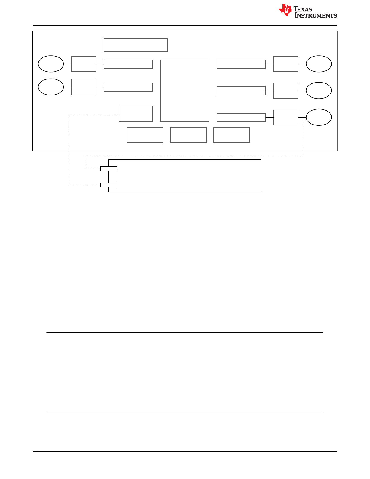
5 Brief Description of Safety Elements
This section contains a brief description of the elements on the TMS320F28002x MCU device family, organized
based on the classification of parts of generic hardware of a system [8] as indicated in Figure 5-1. For a full
functional description of any of these modules, see the device-specific technical reference manual. The brief
description of the hardware part is followed by the list of primary safety mechanisms that can be employed
to provide diagnostic coverage to the hardware part. Some safety standards have the requirement to provide
diagnostic coverage for the primary diagnostic measures (for example, Latent Fault Metric requirement from
ISO 26262:2018). These measures are called as test of diagnostics. Primary diagnostics of type “Software” and
“Hardware/Software” involves execution of the software on the processing units and also use many of the MCU
parts like Interconnect, Memory (Flash, SRAM and ROM) and TMS320F28002x MCU infrastructure components
(Clock, Power, Reset and JTAG). In order to ensure integrity of the implemented primary diagnostics and their
associated diagnostic coverage values, measures to protect execution of primary diagnostics on respective
processing units needs to be implemented. Appropriate combination of test of diagnostics is recommended to be
implemented for parts of the MCU contributing the successful operation of the processing units. For diagnostics
for these parts, see the respective sections in this safety manual.
In case, separate test of diagnostic measures exist for a primary diagnostic measure, they are mentioned along
with the respective hardware part.
SPRUIT5 – APRIL 2021
Submit Document Feedback
Safety Manual for TMS320F28002x 17
Copyright © 2021 Texas Instruments Incorporated
Page 18
D.2 E/E System
D.2 E/E System
D.11
Sensor
D.11
Sensor
D.3
Connector
D.3
Connector
D.7 Digital I.
D.7 Analogue I.
D.8 Bus interface
D.9 Power Supply
D.4
Processing Unit
D.3 Relay
D.7 Digital O.
D.7 Analogue O.
D.3
Connector
D.3
Connector
D.3
Connector
D.12
Actuator
D.12
Actuator
D.12
Actuator
D.6 RAM D.5 ROM D.10 Clock
Brief Description of Safety Elements
www.ti.com
Figure 5-1. Generic Hardware of a System
5.1 TMS320F28002x MCU Infrastructure Components
5.1.1 Power Supply
The C2000 MCU device family requires an external device to supply the necessary voltage and current for
proper operation. Separate voltage rails are available for core (1.2 V), Analog (3.3 V), Flash (3.3 V) and I/O logic
(3.3 V). Following mechanisms can be used to improve the diagnostic coverage of C2000 MCU power supply.
• External Voltage Supervisor
• External Watchdog (using GPIO or a serial interface)
• Internal Watchdog (WD)
• Brownout Reset (BOR)
• Multi-Bit Enable Keys for Control Registers
• Lock Mechanism for Control Registers
• Software Read Back of Written Configuration
• Periodic Software Read Back of Static Configuration Registers
• Online Monitoring of Temperature
• EALLOW and MEALLOW Protection for Critical Registers
• Having independent voltage supervision at system level is an assumption used while performing
safety analysis.
• Devices can be implemented with multiple power rails that are intended to be ganged together on
the system PCB. For proper operation of power diagnostics, it is recommended to implement one
voltage supervisor per ganged rail.
• Common mode failure analysis of the external voltage supervisor along with TMS320F28002x
MCU is useful to determine dependencies in the voltage generation and supervision circuitry.
• Customer can consider using TI's TPS6538x power supply and safety companion device for
voltage supervision at system level.
Note
18 Safety Manual for TMS320F28002x SPRUIT5 – APRIL 2021
Copyright © 2021 Texas Instruments Incorporated
Submit Document Feedback
Page 19

www.ti.com
Brief Description of Safety Elements
5.1.2 Clock
The TMS320F28002x MCU device family products are primarily synchronous logic devices and as such require
clock signals for proper operation. The clock management logic includes clock sources, clock generation logic
including clock multiplication by phase lock loops (PLLs), clock dividers, and clock distribution logic. The
registers that are used to program the clock management logic are located in the system control module.
The following tests can be applied as diagnostics for this module (to provide diagnostic coverage on a specific
function):
• Missing Clock Detect (MCD)
• Clock Integrity Check Using CPU Timer
• Clock Integrity Check Using HRPWM
• Dual clock comparator (DCC) - Type0
• External Monitoring of Clock via XCLKOUT
• Internal Watchdog (WD)
• External Watchdog
• Periodic Software Read Back of Static Configuration Registers
• Software Read Back of Written Configuration
• PLL Lock Profiling Using On-Chip Timer
• Peripheral Clock Gating (PCLKCR)
• Efuse CRC
• Hardware disable of JTAG port
The following tests can be applied as test-for-diagnostics on this module to meet Latent Fault Metric
Requirements:
• Software Test of Watchdog (WD) Operation
• Software Test of Missing Clock Detect Functionality
Note
• Higher diagnostic coverage can be obtained by setting tighter bounds when checking clock
integrity using Timer2.
• TI recommends the use of an external watchdog over an internal watchdog for mitigating the risk
due to common mode failure. TI also recommends the use of a program sequence, windowed, or
question and answer watchdog as opposed to a single threshold watchdog due to the additional
failure modes that can be detected by a more advanced watchdog.
• Driving a high-frequency clock output on the XCLKOUT pin may have EMI implications. The
selected clock needs to be scaled suitably before sending out through IO.
5.1.3 System PLL
The TMS320F28002x MCU device family products are primarily synchronous logic devices and as such
require clock signals for proper operation. One of the important module for clock generation logic is the clock
multiplication by phase lock loops (PLL).
The following tests can be applied as diagnostics for this module (to provide diagnostic coverage on a specific
function):
• Clock integrity check using DCC
• PLL lock indication
• Internal Watchdog (WD)
• External Watchdog
• Software test of DCC functionality including error tests
• External monitoring of Clock
• Interleaving of FSM states
• Hardware disable of JTAG port
The following tests can be applied as test-for-diagnostics on this module to meet Latent Fault Metric
Requirements:
SPRUIT5 – APRIL 2021
Submit Document Feedback
Copyright © 2021 Texas Instruments Incorporated
Safety Manual for TMS320F28002x 19
Page 20

Brief Description of Safety Elements
www.ti.com
• Software test of functionality including error tests
• Software test of Watchdog (WD) operation
5.1.4 Reset
The power-on reset (PORn) generates an internal warm reset signal to reset the majority of digital logic as part
of the boot process. The warm reset can also be provided at device level as an I/O pin (XRSn) with open drain
implementation. Diagnostic capabilities like NMI watchdog and Watchdog are capable of issuing a warm reset.
For more information on the reset functionality, see the device-specific data sheet.
The following tests can be applied as diagnostics for this module to provide diagnostic coverage on a specific
function.
• External Monitoring of Warm Reset (XRSn)
• Reset Cause Information
• Software Test of Reset
• Glitch Filtering on Reset Pins
• NMIWD Shadow Registers
• Periodic Software Read Back of Static Configuration Registers
• Software Read Back of Written Configuration
• NMIWD Reset Functionality
• Peripheral Soft Reset (SOFTPRES)
• Internal Watchdog (WD)
• External Watchdog
The following tests can be applied as test-for-diagnostics on this module to meet Latent Fault Metric
Requirements:
• Software Test of Watchdog (WD) Operation
Note
• Internal watchdogs are not a viable option for reset diagnostics as the monitored reset signals
interact with the internal watchdogs.
• Customer can consider using TI TPS6538x power supply and safety companion device for reset
supervision at system level.
5.1.5 System Control Module and Configuration Registers
The system control module contains the memory-mapped registers to configure clock, analog peripherals
settings and other system related controls. The system control module is also responsible for generating the
synchronization of system resets and delivering the warm reset (XRSn). The configuration registers include the
registers within peripherals that are not required to be updated periodically.
The following tests can be applied as diagnostics for this module (to provide diagnostic coverage on a specific
function):
• Multi-Bit Enable Keys for Control Registers
• Lock Mechanism for Control Registers
• Software Read Back of Written Configuration
• Periodic Software Read Back of Static Configuration Registers
• Online Monitoring of Temperature
• Peripheral Clock Gating (PCLKCR)
• Peripheral Soft Reset (SOFTPRES)
• EALLOW and MEALLOW Protection for Critical Registers
• Software Test of ERRORSTS Functionality
20 Safety Manual for TMS320F28002x SPRUIT5 – APRIL 2021
Copyright © 2021 Texas Instruments Incorporated
Submit Document Feedback
Page 21

www.ti.com
Brief Description of Safety Elements
Note
• Review the Clock and Reset sections as these features are closely controlled by the system
control module.
• Customer can consider using TI TPS6538x power supply and safety companion device for
ERRORSTS pin supervision at system level.
5.1.6 Efuse Static Configuration
The TMS320F28002x MCU device family supports a boot time configuration of certain functionality (such as trim
values for analog macros) with the help of Efuse structures. The Efuses are read automatically after power-on
reset by an autoload function.
The following tests can be applied as diagnostics for this module (to provide diagnostic coverage on a specific
function):
• Efuse Autoload Self-Test
• Efuse ECC
The following tests can be applied as a test-for-diagnostic on this module:
• Efuse ECC Logic Self-Test
• SRAM Parity
• Software Test of SRAM
• VCRC Auto Coverage
5.1.7 JTAG Debug, Trace, Calibration, and Test Access
The TMS320F28002x MCU device family supports debug, test, and calibration implemented over an IEEE
1149.1 JTAG debug port. The physical debug interface is internally connected to a TI debug logic (ICEPICK),
which arbitrates access to test, debug, and calibration logic. Boundary scan is connected in parallel to the
ICEPICK to support usage without preamble scan sequences for easiest manufacturing board test. The following
tests can be applied as diagnostics for this module (to provide diagnostic coverage on a specific function):
• Hardware Disable of JTAG Port
• Internal Watchdog (WD)
• External Watchdog
5.2 Processing Elements
5.2.1 C28x Central Processing Unit (CPU)
The CPU is a 32-bit fixed-point processor with Floating point, CRC Unit (VCRC) and Trigonometric Math Unit
(TMU) co-processors. This device draws from the best features of digital signal processing; reduced instruction
set computing (RISC); and microcontroller architectures, firmware, and tool sets. The CPU features include a
modified Harvard architecture and circular addressing. The RISC features are single-cycle instruction execution,
and register-to-register operations. The modified Harvard architecture of the CPU enables instruction and data
fetches to be performed in parallel. The CPU does this over six separate address/data buses. Its unique
architecture makes it amenable to integrate safety features external to CPU but on chip, to provide improved
diagnostic coverage.
5.2.2 Diagnostics for CPU
The following tests can be applied as diagnostics for this module (to provide diagnostic coverage on a specific
function):
• CPU Hardware Built-In Self-Test (HWBIST)
• Periodic Software Read Back of Static Configuration Registers
• Access Protection Mechanism for Memories
• Hardware Disable of JTAG Port
• CPU Handling of Illegal Operation, Illegal Results and Instruction Trapping
• Internal Watchdog (WD)
• External Watchdog
• Information Redundancy Techniques
SPRUIT5 – APRIL 2021
Submit Document Feedback
Copyright © 2021 Texas Instruments Incorporated
Safety Manual for TMS320F28002x 21
Page 22

Brief Description of Safety Elements
• Stack Overflow Detection
• Embedded Real Time Analysis and Diagnostic (ERAD)
The following tests can be applied as test-for-diagnostics on this module:
• CPU Hardware Built-In Self-Test (HWBIST) Auto Coverage
• CPU Hardware Built-In Self-Test (HWBIST) Fault Injection Capability
• CPU Hardware Built-In Self-Test (HWBIST) Timeout Feature
• VCRC Auto Coverage
• Inbuilt hardware redundancy in ERAD bus comparator module
Note
Measures to mitigate Common Cause Failure in CPU Subsystem: Common-cause failures are one
of the important failure modes when a safety-related design is implemented in a silicon device. The
contribution of hardware and software dependent failures is estimated on a qualitative basis because
no general and sufficiently reliable method exists for quantifying such failures. System Integrator
should perform a detailed analysis based on the inputs from ISO 26262-11:2018, Section 4.7 and IEC
61508-2:2010 Annex E (BetaIC method).
5.2.3 Floating Point Unit (FPU)
The FPU extends the capabilities of C28x CPU by adding registers and instructions to support IEEE singleprecision floating-point operations. For more details on programming FPU please refer to TMS320C28x
Extended Instruction Sets Technical Reference Manual
www.ti.com
The following tests can be applied as diagnostics for this module (to provide diagnostic coverage on a specific
function):
• CPU Hardware Built-In Self-Test (HWBIST)
• Internal Watchdog (WD)
• External Watchdog
• Information Redundancy Techniques
• Stack Overflow Detection
• Embedded Real Time Analysis and Diagnostic (ERAD)
• Hardware Disable of JTAG Port
The following tests can be applied as test-for-diagnostics on this module to meet Latent Fault Metric
Requirements:
• CPU Hardware Built-In Self-Test (HWBIST) Auto Coverage
• CPU Hardware Built-In Self-Test (HWBIST) Fault Injection Capability
• CPU Hardware Built-In Self-Test (HWBIST) Timeout Feature
5.3 Memory (Flash, SRAM and ROM)
5.3.1 Embedded Flash Memory
The embedded Flash memory is a non-volatile memory that is tightly coupled to the C28x CPU. Each CPUSS
have its own dedicated flash memory. The Flash memory is not accessible by DMA. The Flash memory is
primarily used for CPU instruction access, though data access is also possible. Access to the Flash memory can
take multiple CPU cycles depending upon the device frequency and flash wait state configuration. Flash wrapper
logic provides prefetch and data cache to improve performance.
22 Safety Manual for TMS320F28002x SPRUIT5 – APRIL 2021
Copyright © 2021 Texas Instruments Incorporated
Submit Document Feedback
Page 23

www.ti.com
Brief Description of Safety Elements
5.3.2 Diagnostics for Embedded Flash
The following tests can be applied as diagnostics for this module (to provide diagnostic coverage on a specific
function):
• Flash ECC
• VCRC Check of Static Memory Contents
• Bit Multiplexing in Flash Memory Array
• Periodic Software Read Back of Static Configuration Registers
• Software Read Back of Written Configuration
• Flash Program Verify and Erase Verify Check
• Software Test of Flash Prefetch, Data Cache and Wait-States
• Internal Watchdog (WD)
• External Watchdog
• CPU Handling of Illegal Operation, Illegal Results and Instruction Trapping
• Information Redundancy Techniques
The following tests can be applied as test-for-diagnostics on this module:
• Software Test of ECC Logic
• VCRC Auto Coverage
5.3.3 Embedded SRAM
The TMS320F28002x MCU device family has the following types of SRAMs with different characteristics.
• Dedicated to each CPU (M0, M1)
• Local Shared RAM (LSx RAM)
• Global Shared RAM (GSx RAM)
All these RAMs are highly configurable to achieve control for write access and fetch access from different
masters. All dedicated RAMs are enabled with the ECC feature (both data and address) and shared RAMs are
enabled with the Parity (both data and address) feature. Each RAM has its own controller which implements
access protection, security related features and ECC/Parity features for that RAM.
The following tests can be applied as diagnostics for this module (to provide diagnostic coverage on a specific
function):
• SRAM ECC
• SRAM Parity
• Software Test of SRAM
• Bit Multiplexing in SRAM Memory Array
• Periodic Software Read Back of Static Configuration Registers
• Software Read Back of Written Configuration
• Data Scrubbing to Detect/Correct Memory Errors
• VCRC Check of Static Memory Contents
• Software Test of Function Including Error Tests
• Access Protection Mechanism for Memories
• Lock Mechanism for Control Registers
• Information Redundancy Techniques
• CPU Handling of Illegal Operation, Illegal Results and Instruction Trapping
• Internal Watchdog (WD)
• External Watchdog
• Memory Power-On Self-Test (MPOST)
• Background CRC
SPRUIT5 – APRIL 2021
Submit Document Feedback
Safety Manual for TMS320F28002x 23
Copyright © 2021 Texas Instruments Incorporated
Page 24

Brief Description of Safety Elements
www.ti.com
The following tests can be applied as a test-for-diagnostic on this module:
• Software Test of ECC Logic
• Software Test of Parity Logic
• VCRC Auto Coverage
• Watchdog for Background CRC
5.3.4 Embedded ROM
The TMS320F28002x MCU device family has the following types of ROMs:
• Boot ROM helps to boot the device and contain functions for security initialization, device calibration and
support different boot modes
• Secure ROM functions are not developed to meet any systematic capability compliance (ISO
26262-6:2018/IEC 61508-3:2010) and should not be used in functional safety applications.
The following tests can be applied as diagnostics for this module (to provide diagnostic coverage on a specific
function):
• VCRC Check of Static Memory Contents
• Periodic Software Read Back of Static Configuration Registers
• Software Read Back of Written Configuration
• Software Test of Function Including Error Tests
• CPU Handling of Illegal Operation, Illegal Results and Instruction Trapping
• Internal Watchdog (WD)
• External Watchdog
• Power-Up Pre-Operational Security Checks
• Memory Power-On Self-Test (MPOST)
The following tests can be applied as a test-for-diagnostic on this module:
• VCRC Auto Coverage
5.4 On-Chip Communication Including Bus-Arbitration
5.4.1 Device Interconnect
The device interconnects links the multiples masters and slaves within the device. The device interconnect logic
comprises of static master selection muxes, dynamic arbiters and protocol convertors required for various bus
masters (CPU, DMA) to transact with the peripherals and memories.
The following tests can be applied as diagnostics for this module (to provide diagnostic coverage on a specific
function):
• Software Test of Function Including Error Tests
• Internal Watchdog (WD)
• External Watchdog
• Periodic Software Read Back of Static Configuration Registers
• Software Read Back of Written Configuration
• CPU Handling of Illegal Operation, Illegal Results and Instruction Trapping
• Transmission Redundancy
• Hardware Redundancy
• EALLOW and MEALLOW Protection for Critical Registers
• Timeout detection through ERAD counter
The following tests can be applied as test-for-diagnostics on this module.
• Software test of functionality including error tests
24 Safety Manual for TMS320F28002x SPRUIT5 – APRIL 2021
Copyright © 2021 Texas Instruments Incorporated
Submit Document Feedback
Page 25

www.ti.com
Brief Description of Safety Elements
5.4.2 Direct Memory Access (DMA)
The direct memory access (DMA) module provides a hardware method of transferring data between peripherals
and/or memory without intervention from the CPU, thereby freeing up bandwidth for other system functions.
Additionally, the DMA has the capability to orthogonally rearrange the data as it is transferred as well as
“ping-pong” data between buffers. These features are useful for structuring data into blocks for optimal CPU
processing.
The following tests can be applied as diagnostics for this module (to provide diagnostic coverage on a specific
function):
• Information Redundancy Techniques
• Transmission Redundancy
• Periodic Software Read Back of Static Configuration Registers
• Software Read Back of Written Configuration
• Software Test of Function Including Error Tests
• DMA Overflow Interrupt
• Access Protection Mechanism for Memories
• Software Test of Function Including Error Tests
• Disabling of Unused DMA Trigger Sources
5.4.3 Enhanced Peripheral Interrupt Expander (ePIE) Module
The enhanced Peripheral Interrupt Expander (ePIE) module is used to interface peripheral interrupts to the C28x
CPU. It provides configurable masking on a per interrupt basis. The PIE module includes a local SRAM that is
used to hold the address of the interrupt handler per interrupt.
The following tests can be applied as diagnostics for this module (to provide diagnostic coverage on a specific
function):
• PIE Double SRAM Hardware Comparison
• Software Test of SRAM
• Software Test of ePIE Operation Including Error Tests
• Periodic Software Read Back of Static Configuration Registers
• Software Read Back of Written Configuration
• Maintaining Interrupt Handler for Unused Interrupts
• Online Monitoring of Interrups and Events
The following tests can be applied as a test-for-diagnostic on this module:
• PIE Double SRAM Comparison Check
5.4.4 Dual Zone Code Security Module (DCSM)
The dual code security module (DCSM) is a security feature incorporated in this device. It prevents access and
visibility to on-chip secure memories (and other secure resources) to unauthorized persons. It also prevents
duplication and reverse engineering of proprietary code.
The following tests can be applied as diagnostics for this module (to provide diagnostic coverage on a specific
function):
• Multi-Bit Enable Keys for Control Registers
• Majority Voting and Error Detection of Link Pointer
• Periodic Software Read Back of Static Configuration Registers
• Software Test of Function Including Error Tests
• Software Read Back of Written Configuration
• CPU Handling of Illegal Operation, Illegal Results and Instruction Trapping
• VCRC Check of Static Memory Contents
• External Watchdog
• Hardware Redundancy
The following test can be applied as a test-for-diagnostic on this module:
• VCRC Auto Coverage
SPRUIT5 – APRIL 2021
Submit Document Feedback
Copyright © 2021 Texas Instruments Incorporated
Safety Manual for TMS320F28002x 25
Page 26

Brief Description of Safety Elements
www.ti.com
5.4.5 CrossBar (X-BAR)
The crossbars (X-BAR) provide flexibility to connect device inputs, outputs, and internal resources in a variety
of configurations. The device contains a total of four X-BARs: Input X-BAR, Output X-BAR, CLB X-BAR and
ePWM X-BAR. The Input X-BAR has access to every GPIO and can route each signal to any (or multiple) of
the IP blocks (for example, ADC, eCAP, ePWM, and so forth). This flexibility relieves some of the constraints on
peripheral muxing by just requiring any GPIO pin to be available. The ePWM X-BAR is connected to the Digital
Compare (DC) sub-module of each ePWM module for actions such as trip zones. The GPIO Output X-BAR
takes signals from inside the device and brings them out to a GPIO. The CLB X-BAR has eight outputs that are
connected to the CLB global mux as AUXSIGx.
The following tests can be applied as diagnostics for this module (to provide diagnostic coverage on a specific
function):
• Software Test of Function Including Error Tests
• Hardware Redundancy
• Periodic Software Read Back of Static Configuration Registers
• Software Read Back of Written Configuration
• Software Check of X-BAR Flag
5.4.6 Timer
The CPU subsystem is provided with three 32-bit CPU-Timers (TIMER0/1/2). The module provides the
Operating System (OS) timer for the device. The OS timer function is used to generate internal event triggers
or interrupts as needed to provide periodic operation of safety critical functions. The capabilities of the module
enable it to be used for clock monitoring as well.
The following tests can be applied as diagnostics for this module (to provide diagnostic coverage on a specific
function):
• 1oo2 Software Voting Using Secondary Free Running Counter
• Periodic Software Read Back of Static Configuration Registers
• Software Read Back of Written Configuration
• Software Test of Function Including Error Tests
5.4.7 Configurable Logic Block
The Configurable logic block (CLB) is a collection of blocks that can be interconnected using software to
implement custom digital logic functions or enhance existing on-chip peripherals. The CLB is able to enhance
existing peripherals through a set of crossbar interconnections, which provide a high level of connectivity to
existing control peripherals such as enhanced pulse width modulators (ePWM), enhanced capture modules
(eCAP), and enhanced quadrature encoder pulse modules (eQEP). The crossbars also allow the CLB to be
connected to external GPIO pins. In this way, the CLB can be configured to interact with device peripherals to
perform small logical functions such as comparators, or to implement custom serial data exchange protocols.
Through the CLB, functions that would otherwise be accomplished using external logic devices can now be
implemented inside the MCU. CLB can be used to implement Absolute or Incremental Position Encoders used
for Motor control applications.
The CLB peripheral is configured through the CLB tool. More information on the CLB tool, available examples,
application reports and users guide are avaialble in C2000Ware under \utilities\clb_tool.
The following tests can be applied as diagnostics for this module (to provide diagnostic coverage on a specific
function):
• Software Test of CLB Function including Error Tests
• Hardware Redundancy
• Monitoring of CLB by eCAP or eQEP
• Periodic Software Read Back of static Configuration Registers
• Software Read Back of Written Configuration
• Lock Mechanism of Control Regsiters
• Internal Watchdog (WD)
• Periodic Read Back of SPI Buffer
26 Safety Manual for TMS320F28002x SPRUIT5 – APRIL 2021
Copyright © 2021 Texas Instruments Incorporated
Submit Document Feedback
Page 27

www.ti.com
Brief Description of Safety Elements
• Hardware Disable of JTAG Port
5.5 Digital I/O
5.5.1 General-Purpose Input/Output (GPIO) and Pinmuxing
The General Purpose Input/Output (GPIO) module provides software configurable mapping of internal module
I/O functionality to device pins. These pins can be individually selected to operate as digital I/O (also called
GPIO mode), or connected to one of several peripheral I/O signals.
The following tests can be applied as diagnostics for this module (to provide diagnostic coverage on a specific
function):
• Lock Mechanism for Control Registers
• Periodic Software Read Back of Static Configuration Registers
• Software Read Back of Written Configuration
• Software Test of Function Using I/O Loopback
• Hardware Redundancy
5.5.2 Enhanced Pulse Width Modulators (ePWM)
The enhanced Pulse Width Modulator (ePWM) peripheral is a key element in digital motor control and power
electronic systems. Some of the ePWM module instances support a High-Resolution Pulse Width Modulator
(HRPWM) mode to improve the time resolution. For more information on the ePWM instances supporting the
HRPWM mode, see the device-specific data sheet and reference manual.
The following tests can be applied as diagnostics for this module (to provide diagnostic coverage on a specific
function):
• Software Test of Function Including Error Tests
• Hardware Redundancy
• Monitoring of ePWM by eCAP
• Periodic Software Read Back of Static Configuration Registers
• Software Read Back of Written Configuration
• Lock Mechanism for Control Registers
• ePWM Fault Detection using XBAR
• ePWM Synchronization Check
• ePWM Application Level Safety Mechanism
• Online Monitoring of Interrupts and Events
• Monitoring of ePWM by ADC
5.5.3 High Resolution PWM (HRPWM)
HRPWM module extends the time resolution capabilities of the conventionally derived digital pulse width
modulator (PWM). HRPWM is typically used when PWM resolution falls below ~ 9-10 bits. The HRPWM is
based on micro edge positioner (MEP) technology. MEP logic is capable of positioning an edge very finely by
sub-dividing one coarse system clock of a conventional PWM generator. The time step accuracy is of the order
of 150 ps.
The following tests can be applied as diagnostics for this module (to provide diagnostic coverage on a specific
function):
• HRPWM Built-In Self-Check and Diagnostic Capabilities
• Hardware Redundancy
• Monitoring of ePWM by eCAP
• Periodic Software Read Back of Static Configuration Registers
• Software Read Back of Written Configuration
• Lock Mechanism for Control Registers
5.5.4 Enhanced Capture (eCAP)
The enhanced CAPture (eCAP) module provides input capture functionality for systems where accurate timing
of external events is important. The eCAP module features include speed measurements of rotating machinery
(for example, toothed sprockets sensed via Hall sensors), elapsed time measurements between position sensor
SPRUIT5 – APRIL 2021
Submit Document Feedback
Copyright © 2021 Texas Instruments Incorporated
Safety Manual for TMS320F28002x 27
Page 28

Brief Description of Safety Elements
www.ti.com
pulses, period and duty cycle measurements of pulse train signals and decoding current or voltage amplitude
derived from duty cycle encoded current/voltage sensors.
The following tests can be applied as diagnostics for this module (to provide diagnostic coverage on a specific
function):
• Software Test of Function Including Error Tests
• Information Redundancy Techniques
• Monitoring of ePWM by eCAP
• Periodic Software Read Back of Static Configuration Registers
• Software Read Back of Written Configuration
• eCAP Application Level Safety Mechanism
• Hardware Redundancy
Note
Use of a sensorless positioning algorithm can provide information redundancy through plausibility
checking of eCAP results.
5.5.5 High Resolution Capture (HRCAP)
The high-resolution capture (HRCAP) peripheral measures the width of external pulses with a typical resolution
within hundreds of picoseconds. This module includes capture channel in addition to a HW calibration block to
enable continuous on-line calibration, this drastically reduces software overhead to calibrate. HRCAP input can
be connected to HRPWM output using X-BAR to enable periodic testing. The HRCAP enhancement has been
added to eCAP 6 and eCAP 7.
The following tests can be applied as diagnostics for this module (to provide diagnostic coverage on a specific
function):
• Software Test of Function Including Error Tests
• Hardware Redundancy
• Monitoring of HRPWM by HRCAP
• Periodic Software Read Back of Static Configuration Registers
• Software Read Back of Written Configuration
• HRCAP Calibration Logic Test Feature
5.5.6 Enhanced Quadrature Encoder Pulse (eQEP)
The enhanced Quadrature Encoder Pulse (eQEP) module is used for direct interface with a linear or rotary
incremental encoder to get position, direction, and speed information from a rotating machine for use in a
high-performance motion and position-control system. The following tests can be applied as diagnostics for this
module (to provide diagnostic coverage on a specific function):
• Software Test of Function Including Error Tests
• eQEP Quadrature Watchdog
• Information Redundancy Techniques
• Periodic Software Read Back of Static Configuration Registers
• Software Read Back of Written Configuration
• eQEP Application Level Safety Mechanisms
• Hardware Redundancy
The following tests can be applied as a test-for-diagnostic on this module:
• eQEP Software Test of Quadrature Watchdog Functionality
Note
Use of a sensorless positioning algorithm can provide information redundancy through plausibility
checking of eQEP results.
28 Safety Manual for TMS320F28002x SPRUIT5 – APRIL 2021
Copyright © 2021 Texas Instruments Incorporated
Submit Document Feedback
Page 29

www.ti.com
Brief Description of Safety Elements
5.5.7 External Interrupt (XINT)
Interrupts from external sources can be provided to the device using GPIO pins with help of XINT module. The
module allows configuring the GPIOs to be selected as interrupt sources. The polarity of the interrupts can also
be configured with this module.
The following tests can be applied as diagnostics for this module (to provide diagnostic coverage on a specific
function):
• Software Test of Function Including Error Tests
• Periodic Software Read Back of Static Configuration Registers
• Software Read Back of Written Configuration
• Hardware Redundancy
5.6 Analog I/O
5.6.1 Analog-to-Digital Converter (ADC)
The Analog-to-Digital Converter (ADC) module is used to convert analog inputs into digital values. Results are
stored in internal registers for later transfer by DMA or CPU. The TMS320F28002x MCU device family products
implement up to two modules with shared channels used for fast conversion (ping-pong method).
The following tests can be applied as diagnostics for this module (to provide diagnostic coverage on a specific
function):
• Software Test of Function Including Error Tests
• DAC to ADC Loopback Check
• ADC Information Redundancy Techniques
• Opens/Shorts Detection Circuit for ADC
• Software Read Back of Written Configuration
• Periodic Software Read Back of Static Configuration Registers
• ADC Signal Quality Check by Varying Acquisition Window
• ADC Input Signal Integrity Check
• Monitoring of ePWM by ADC
• Hardware Redundancy
• Disabling Unused Sources of SOC Inputs to ADC
Note
• ADC module voltages should be supervised as noted in the device-specific data sheet.
• To reduce probability of common mode failure, user should consider implementing multiple
channels (information redundancy) using non adjacent pins and different voltage reference.
SPRUIT5 – APRIL 2021
Submit Document Feedback
Safety Manual for TMS320F28002x 29
Copyright © 2021 Texas Instruments Incorporated
Page 30

Brief Description of Safety Elements
www.ti.com
5.6.2 Comparator Subsystem (CMPSS)
The Comparator Subsystem (CMPSS) consists of analog comparators and supporting components that are
combined into a topology that is useful for power applications such as peak current mode control, switchedmode power, power factor correction, and voltage trip monitoring. The comparator subsystem is built around a
pair of analog comparators and helps detection of signal exception conditions including High/Low thresholds.
The positive input of the comparator is always driven from an external pin, but the negative input can be driven
by either an external pin or by an internal programmable 12-bit DAC. Each comparator output passes through a
programmable digital filter that can remove spurious trip signals. A ramp generator circuit is optionally available
to control the internal DAC value for one comparator in the subsystem.
The following tests can be applied as diagnostics for this module (to provide diagnostic coverage on a specific
function):
• Software Test of Function Including Error Tests
• Hardware Redundancy
• Software Read Back of Written Configuration
• Periodic Software Read Back of Static Configuration Registers
• Lock Mechanism for Control Registers
• VDAC Conversion by ADC
• CMPSS Ramp Generator Functionality Check
5.7 Data Transmission
5.7.1 Controller Area Network (DCAN)
The Controller Area Network (DCAN) interface provides medium throughput networking with event based
triggering, compliant to the CAN protocol. The DCAN modules requires an external transceiver to operate on the
CAN network. The following tests can be applied as diagnostics for this module (to provide diagnostic coverage
on a specific function):
• Software Test of Function Using I/O Loopback
• Information Redundancy Techniques Including End-to-End Safing
• SRAM Parity
• Software Test of SRAM
• Bit Multiplexing in SRAM Memory Array
• Periodic Software Read Back of Static Configuration Registers
• Software Read Back of Written Configuration
• Transmission Redundancy
• DCAN Stuff Error Detection
• DCAN Form Error Detection
• DCAN Acknowledge Error Detection
• Bit Error Detection
• CRC in Message
• Hardware Redundancy
The following tests can be applied as a test-for-diagnostic on this module:
• Software Test of Parity Logic
30 Safety Manual for TMS320F28002x SPRUIT5 – APRIL 2021
Copyright © 2021 Texas Instruments Incorporated
Submit Document Feedback
Page 31

www.ti.com
Brief Description of Safety Elements
5.7.2 Serial Peripheral Interface (SPI)
The Serial Peripheral Interface (SPI) modules provide serial I/O compliant to the SPI protocol. SPI
communications are typically used for communication to smart sensors and actuators, serial memories, and
external logic such as a watchdog device.
The following tests can be applied as diagnostics for this module (to provide diagnostic coverage on a specific
function):
• Software Test of Function Using I/O Loopback
• Information Redundancy Techniques Including End-to-End Safing
• Periodic Software Read Back of Static Configuration Registers
• Software Read Back of Written Configuration
• Transmission Redundancy
• SPI Data Overrun Detection
• Hardware Redundancy
5.7.3 Serial Communication Interface (SCI)
The module provides serial I/O capability for typical asynchronous Serial Communication Interface (SCI)
protocols, such as UART. Depending on the serial protocol used, an external transceiver may be necessary.
The following tests can be applied as diagnostics for this module (to provide diagnostic coverage on a specific
function):
• Software Test of Function Using I/O Loopback
• Parity in Message
• Information Redundancy Techniques Including End-to-End Safing
• Overrun Error Detection
• SCI Break Error Detection
• Frame Error Detection
• Periodic Software Read Back of Static Configuration Registers
• Software Read Back of Written Configuration
• Transmission Redundancy
• Hardware Redundancy
5.7.4 Inter-Integrated Circuit (I2C)
The Inter-Integrated Circuit (I2C) module provides a multi-master serial bus compliant to the I2C protocol. The
following tests can be applied as diagnostics for this module (to provide diagnostic coverage on a specific
function):
• Software Test of Function Using I/O Loopback
• I2C Data Acknowledge Check
• Information Redundancy Techniques Including End-to-End Safing
• Periodic Software Read Back of Static Configuration Registers
• Software Read Back of Written Configuration
• Transmission Redundancy
• I2C Access Latency Profiling Using On-Chip Timer
5.7.5 Fast Serial Interface (FSI)
The Fast Serial Interface (FSI) is a serial peripheral capable of reliable and high-speed communication. The FSI
is architected specifically to ensure reliable and high-speed communication for those system scenarios involving
communication across isolation devices. The FSI consists of independent transmitter (FSITX) and receiver
(FSIRX) cores. The FSITX and FSIRX cores are configured and operated independently.
SPRUIT5 – APRIL 2021
Submit Document Feedback
Safety Manual for TMS320F28002x 31
Copyright © 2021 Texas Instruments Incorporated
Page 32

Brief Description of Safety Elements
www.ti.com
The following tests can be applied as diagnostics for this module (to provide diagnostic coverage on a specific
function):
• Software Test of Function Using I/O Loopback Including Error Tests
• Information Redundancy Techniques Including End-to-End Safing
• Periodic Software Read Back of Static Configuration Registers
• Software Read Back of Written Configuration
• Transmission Redundancy
• FSI Data Overrun/Underrun Detection
• FSI Frame Overrun Detection
• FSI CRC Framing Checks
• FSI ECC Framing Checks
• FSI Frame Watchdog
• FSI RX Ping Watchdog
• FSI Tag Monitor
• FSI Frame Type Error Detection
• FSI End of Frame Error Detection
• FSI Register Protection Mechanisms
5.7.6 Local Interconnect Network (LIN)
The LIN module supported is compliant to the LIN 2.1 protocol specification. This module can be programmed to
work either as an SCI or as a LIN. The SCI’s hardware features are augmented to achieve LIN functionality. The
SCI module is a universal asynchronous receiver-transmitter (UART) that implements the standard non-return to
zero format. The SCI can be used to communicate, for example, through an RS-232 port or over a K line.
The following tests can be applied as diagnostics for this module (to provide diagnostic coverage on a specific
function):
• Software Test of Function Using I/O Loopback
• Information Redundancy Techniques Including End-to-End Safing
• Transmission Redundancy
• Periodic Software Read Back of Static Configuration Registers
• Software Read Back of Written Configuration
• Data Parity Error Detection
• Overrun Error Detection
• Frame Error Detection
• LIN Physical Bus Error Detection
• LIN No-Response Error Detection
• Bit Error Detection
• Checksum Error Detection
• LIN ID Parity Error Detection
• SCI Break Error Detection
• Communication Access Latency Profiling Using On-Chip Timer
32 Safety Manual for TMS320F28002x SPRUIT5 – APRIL 2021
Copyright © 2021 Texas Instruments Incorporated
Submit Document Feedback
Page 33

www.ti.com
Brief Description of Safety Elements
5.7.7 Power Management Bus Module (PMBus)
The PMBus module provides an interface between the microcontroller and devices compliant with the SMI
Forum PMBus Specification Part I version 1.0 and Part II version 1.1. PMBus is based on SMBus, which uses a
similar physical layer to I2C.This module supports both master and slave modes.
The following tests can be applied as diagnostics for this module (to provide diagnostic coverage on a Specific
function):
• I2C Data Acknowledge Check
• Information Redundancy Techniques Including End to End Safing
• Periodic Software Read Back of Static Configuration Registers
• Software Read Back of Written Configuration
• Transmission Redundancy
• PMBus Protocol CRC in Message
• Clock Timeout
5.7.8 Host Interface Controller (HIC)
The Host Interface Controller (HIC) module allows an external host controller (master) to directly access
resources of the device (slave) by emulating the ASRAM protocol. It has two modes of operation: direct access
and mailbox access. In direct access mode, device resources is written to and read from directly by the external
host. In mailbox access mode, external host and device write to and read from a buffer and notify each other
when the buffer write/read is complete. For security reasons, the HIC has to be enabled by the device before the
external host can access it.
The following tests can be applied as diagnostics for this module (to provide diagnostic coverage on a specific
function):
• Periodic Software Read Back of Static Configuration Registers
• Signature mechanism for interrupt and acknowledgement in software
• Software timeout mechanism for interrupt logic
• Access protection enable for read/write operations in software
• Software Read Back of Written Configuration
• Detection of illegal access sequences or access types from host to device
• Detection of simultaneous MMR access by host and device
• Enabling the locking mechanism for registers
• Software test of function including error tests
• Transmission Redundancy
• Information Redundancy Techniques Including End-to-End Safing
• Disabling of unused EVENTRIG trigger sources
• Internal Watchdog (WD)
• Hardware Disable of JTAG Port
SPRUIT5 – APRIL 2021
Submit Document Feedback
Safety Manual for TMS320F28002x 33
Copyright © 2021 Texas Instruments Incorporated
Page 34

Brief Description of Diagnostics
www.ti.com
6 Brief Description of Diagnostics
This section provides a brief summary of the diagnostic mechanisms available on the TMS320F28002x MCU
device family. The diagnostic mechanisms are arranged as per the device portioning given in Figure 5-1. At
places where the safety mechanism is applicable for more than one component, it is placed at an appropriate
place based on the applicable use case scenario. For a detailed description or implementation details for a
diagnostic, see the device-specific technical reference manual.
6.1 TMS320F28002x MCU Infrastructure Components
6.1.1 Clock Integrity Check Using CPU Timer
It is recommended to use the CPU Timer module to detect incorrect clock frequencies and drift between clock
sources. CPU Timer2 has a programmable counter whose prescale value and clock source can be selected.The
frequency relationship between selected clock and system clock can be determined by using the system clock
as a reference time base. For more information on the clock selection options implemented, see the devicespecific data sheet. Higher diagnostic coverage can be obtained by setting tighter bounds when checking clock
integrity using Timer2. Common cause failures can be reduced by using different clock sources and different
prescale values for the reference clock and measured clock. The Timer diagnostic is not enabled by default and
must be enabled via software. The cyclical check applied by the Timer module provides an inherent level of
self-checking (auto-coverage), which can be considered for application in latent fault diagnostics.
6.1.2 Clock Integrity Check Using HRPWM
Calibration logic of OTTO (HRPWM) can be used to detect incorrect system clock (SYSCLK) frequencies. The
clock whose frequency needs to be measured is configured as the system clock and the auto-calibration function
is executed. The result obtained from the calibration function can be checked against the predetermined range
of values to detect incorrect clock frequency or frequency drift. Error response, diagnostic testability, and any
necessary software requirements are defined by the software implemented by the system integrator.
6.1.3 Clock Integrity Check Using DCC
One of more dual clock comparators (DCC) are implemented as multi-purpose safety diagnostics. The DCC can
be used to detect incorrect frequencies and drift between clock sources. The DCC is composed of two counter
blocks, one is used as a reference time base and the second is used for the clock under test. Both reference
clock and clock under test may be selected via software, as can the expected ratio of the clock frequencies.
Deviation from the expected ratio generated an error indication to the ESM. For more information on the clock
selection options implemented, refer to the device data sheet. For DCC programming details, refer the device
technical reference manual (TRM).
The DCC diagnostics is not enabled by default and must be enabled via customer software. It is possible to
disable and configure this diagnostic via software. The cyclical check applied by the DCC module provides
an inherent level of self-checking (auto-coverage), which can be considered for application in latent fault
diagnostics.
6.1.4 EALLOW Protection for Critical Registers
EALLOW (CPU, DMA) protection enables write access to emulation and other protected registers. CPU can set
this bit using EALLOW instruction and cleared using EDIS instruction. The protection can be used to prevent
data being written to the wrong place, which could result from conditions like boundary exceeding, incorrect
pointers, stack overflow or corruption, and so forth. Reads from the protected registers are always allowed. It is
recommended to issue an EDIS for protection once the write of protected registers are complete.
6.1.5 Efuse Autoload Self-Test
Efuse provides a capability to ensure proper loading of the efuse values to all the registers. The capability is
enabled by default and configuration cannot be changed by software. Any error in this process will be indicated
via ERRORSTS. The device reset is asserted and autoload is re-attempted when the error occurs.
34 Safety Manual for TMS320F28002x SPRUIT5 – APRIL 2021
Copyright © 2021 Texas Instruments Incorporated
Submit Document Feedback
Page 35

www.ti.com
Brief Description of Diagnostics
6.1.6 Efuse ECC
The Efuse utilizes a SECDED ECC diagnostic to detect and possibly correct errors in the configuration values
fetched from the fuse ROM. Errors are indicated via ERRORSTS. This diagnostic is ON by default and this
configuration cannot be changed by software. It covers only data bits of the EFUSE ROM. The device reset is
asserted and autoload is re-attempted when the error occurs.
6.1.7 Efuse ECC Logic Self-Test
The Efuse controller has a self-test logic that executes automatically before the efuse operation. Errors are
indicated via ERRORSTS and a system control register. The device will remain in a reset state as long as the
error occurs.
6.1.8 External Monitoring of Clock via XCLKOUT
The TMS320F28002x MCU device family provides the capability to export selected internal clocking signals for
external monitoring. This feature can be configured via software by programming registers in the system control
module. To determine the number of external clock outputs implemented and the register mapping of internal
clocks that can be exported, see the device-specific data sheet. Export of internal clocks on the XCLKOUT
outputs is not enabled by default and must be enabled via software.
6.1.9 External Monitoring of Warm Reset (XRSn)
The XRSn warm reset signal is implemented as an open drain I/O pin. An external monitor can be utilized
to detect expected or unexpected changes to the state of the internal warm reset control signal and ensuring
proper signaling (for example, low duration) when it is asserted. Error response, diagnostic testability, and any
necessary software requirements are defined by the external monitor selected by the system integrator.
6.1.10 External Voltage Supervisor
Texas Instruments highly recommends the use of an external voltage supervisor to monitor all voltage rails
(VDDIO, VDDA, and VDD). The voltage supervisor should be configured with over voltage and under voltage
thresholds within the recommended operating conditions of the target device as noted in the device-specific
data sheet. Error response, diagnostic testability, and any necessary software requirements are defined by the
external voltage supervisor selected by the system integrator.
6.1.11 External Watchdog
External watchdog helps to reduce common mode failure, as it utilizes clock, reset, and power that are
separate from the system being monitored. Error response, diagnostic testability, and any necessary software
requirements are defined by the external watchdog selected by the system integrator.
Texas Instruments highly recommends the use of an external watchdog in addition to the internally provided
watchdogs. An internal or external watchdog can provide an indication of inadvertent activation of logic which
results in impact to safety critical execution. Any watchdog added externally should include a combination of
temporal and logical monitoring of program sequence [IEC 61508-7:2010, clause A.9.3] or other appropriate
methods such that high diagnostic effectiveness can be claimed.
6.1.12 Glitch Filtering on Reset Pins
Glitch filters are implemented on XRSn and JTAG reset of the device. These structures filter out noise and
transient signal spikes on the input reset pins in order to reduce unintended activation of the reset circuitry.
The glitch filters are enabled by default and operates continuously. Their behavior cannot be changed by the
software.
6.1.13 Hardware Disable of JTAG Port
The JTAG debug port can be physically disabled to prevent JTAG access in deployed systems. The
recommended scheme is to hold Test Mode Select (TMS) high. Disabling of the JTAG port also provides
coverage for inadvertent activation of many debug and trace activities.
SPRUIT5 – APRIL 2021
Submit Document Feedback
Copyright © 2021 Texas Instruments Incorporated
Safety Manual for TMS320F28002x 35
Page 36

Brief Description of Diagnostics
www.ti.com
6.1.14 Internal Watchdog (WD)
The internal watchdog has two modes of operation: normal watchdog (WD) and windowed watchdog (WWD).
The system integrator can select to use one mode or the other but not both at the same time. For details
of programming the internal watchdogs, see the device-specific technical reference manual. The WD is a
traditional single threshold watchdog. The user programs a timeout value to the watchdog and must provide a
predetermined WDKEY to the watchdog before the timeout counter expires. Expiration of the timeout counter
or an incorrect WDKEY triggers an error response. The WD can issue either a warm system reset or a CPU
maskable interrupt upon detection of a failure. The WD is enabled after reset.
The use of the time window allows detection of additional clocking failure modes as compared to the WD
implementation. User programs an upper bound and lower bound to create a time window during which the
software must provide a predetermined WDKEY to the watchdog. Failure to receive the correct response within
the time window or an incorrect WDKEY triggers an error response. The WWD can issue either a warm system
reset or a CPU maskable interrupt upon detection of a failure. Normal WD operation is enabled by default after
reset. For details of programming the internal watchdogs, see the device-specific technical reference manual.
In order to avoid common cause failure of clock input to both Internal Watchdog(WD) and CPU, it is
recommended to select either INTOSC2 or X1/X2 as clock source to main PLL.
6.1.15 Lock Mechanism for Control Registers
The module contains a lock mechanism for protection of critical control registers. Once the associated LOCK
register bits are set, the write accesses to the registers are blocked. Locked registers cannot be updated by
software. Once locked, only reset can unlock the registers.
6.1.16 Missing Clock Detect (MCD)
The missing clock detector (MCD) is a safety diagnostic that can be used to detect failure of PLL reference
clock. MCD utilizes the embedded 10 MHz internal oscillator (INTOSC1). This circuit only detects complete loss
of PLL reference clock and doesn’t do any detection of frequency drift. The MCD circuit is enabled by default
during the power-on reset state. The diagnostic can be disabled via software.
6.1.17 NMIWD Reset Functionality
On receiving an NMI, the software can attempt recovery from the NMI condition. Based on the severity and
type of the fault condition, recovery may not always be successful. In such a situation, an additional protection
is provided by having an independent watchdog monitoring the NMI recovery. If the attempted recovery is not
successful, a reset is issued. The timeout for reset can be configured (using NMIWDPRD) based on the FTTI of
the device.
6.1.18 NMIWD Shadow Registers
The use of a two stage cold and warm reset scheme on the device allows the implementation of NMIWD shadow
registers. Shadow registers are reset only by power-on reset. These registers are used to store the NMIFLG
information before reset assertion. This information can be used by the application software to provide additional
information on the NMI status of the device before the last warm reset operation.
6.1.19 Multi-Bit Enable Keys for Control Registers
Some modules include features to support avoidance of unintentional control register update. Implementation
of multi-bit keys for critical control registers is one such feature (for example, EPWM_REGS.EPWMLOCK and
so forth). The multi-bit keys are particularly effective for avoiding unintentional activation. For more details on
the registers for which the diagnostic is applicable, see the device-specific technical reference manual. The
operation of this safety mechanism is continuous and cannot be altered by the software. This mechanism can
be tested by generating software transactions with and without correct keys and observing the updated register
value.
6.1.20 Online Monitoring of Temperature
The internal temperature sensor measures the junction temperature of the device. The output of the sensor can
be sampled with the ADC through an internal connection. This can be enabled on channel ADCIN14 on ADCB
by setting the ENABLE bit in the TSNSCTL register.
36 Safety Manual for TMS320F28002x SPRUIT5 – APRIL 2021
Copyright © 2021 Texas Instruments Incorporated
Submit Document Feedback
Page 37

www.ti.com
Brief Description of Diagnostics
Micro Edge Positioning (MEP) block of HRPWM Built-In Self-Check and Diagnostic Capabilities can also be
used to detect variations in temperature and voltage.
6.1.21 Periodic Software Read Back of Static Configuration Registers
Configuration registers are typically configured once in the beginning and hold their value until the particular
task execution. Periodic read back of configuration registers can provide a diagnostic for inadvertent writes or
disturbances to these registers.
The diagnostic coverage can be improved by extending the test to include read back of the flag registers that are
expected to remain constant (PLL lock status, eQEP phase error flag, and so forth) during the device operation
as well. Error response, diagnostic testability, and any necessary software requirements are defined by the
software implemented by the system integrator.
The diagnostic coverage of some peripherals can be further enhanced by applying some module specific tests
as follows:
• For improving the enhanced peripheral interrupt expander (ePIE) coverage, the PIE flag registers can be
periodically checked to ensure that all pending interrupts are serviced by reading the PIE flag registers
(PIE_CTRL_REGS.PIEIFRx.all) and the peripheral interrupt flag registers.
• While serving the interrupt, the ISR routine can check for interrupt flag in peripherals and PIE module to
ensure that correct interrupt is being serviced.
6.1.22 Peripheral Clock Gating (PCLKCR)
Peripherals can be clock gated on a per peripheral basis. This can be utilized to disable unused features such
that they cannot interfere with active safety functions. This safety mechanism is enabled after reset. Software
must configure and disable this mechanism to use a particular peripheral. It is possible to lock the particular
configuration to avoid inadvertent writes.
6.1.23 Peripheral Soft Reset (SOFTPRES)
Peripherals can be kept in reset on a per peripheral basis. This can be utilized to reset the unused features
such that they cannot interfere with active safety functions. These safety mechanisms are disabled after reset.
Software must configure and enable these mechanisms.
6.1.24 PLL Lock Profiling Using On-Chip Timer
Clock setup for the TMS320F28002x MCU device family includes selecting the appropriate clock source,
configuring the PLL multiplier, waiting for the lock status and switching the clock to the PLL output once the
internal lock status is set. The time required for the PLL lock sequence can be profiled using on-chip timer to
detect faults in the PLL wrapper logic. Once the PLL is locked, the frequency of the output clock can be checked
by using the following:
• Clock Integrity Check Using CPU Timer
• Clock Integrity Check Using HRPWM
• External Clock Monitoring via XCLKOUT to ensure proper clock output
6.1.25 PLL lock indication
PLL Lock functionality is implemented by comparing the difference (error) between the feedback clock and
reference clock through Phase Frequency Detector (PFD). When PLL is in lock and generating the correct
frequency, the difference (error) is <100pS~300pS. Once there is any fault causing the PLL output frequency to
drift, the difference will go outside of that range. In such a case, PLL Lock signal will go from 1 to 0 indicating
PLL is out of lock. The tolerance of PLL lock indication is configurable by software. SoC should use this signal as
a critical interrupt/NMI to take the MCU into a safe state.
6.1.26 Reset Cause Information
The system control module provides a status register (RESC) that latches the cause of the most recent reset
event. Application software executed during boot-up can check the status of this register to determine the cause
of the last reset event. This information can be used by the software to identify the cause and manage failure
recovery if required.
SPRUIT5 – APRIL 2021
Submit Document Feedback
Copyright © 2021 Texas Instruments Incorporated
Safety Manual for TMS320F28002x 37
Page 38

Brief Description of Diagnostics
www.ti.com
6.1.27 Software Read Back of Written Configuration
In order to ensure proper configuration of memory-mapped registers in this module, it is recommended for
software implement a test to confirm proper configuration of all control register by reading back the contents.
This test also provides diagnostic coverage for the peripheral bus interface and peripheral interconnect bridges.
6.1.28 Software Test of ERRORSTS Functionality
As indicated in Figure 4-5, ERRORSTS pin is an integral part of MCU safety concept used for indicating to
an external system about a critical error occurring within in the MCU. Proper functioning of ERRORSTS pin
and error handling of the system external to MCU can be checked by asserting ERRORSTS pin by generating
an error condition using one of the software provided ways (asserting CLOCLKFAIL NMIFLG by updating the
NMIFLGFRC.bit.CLOCKFAIL). Error response, diagnostic testability, and any necessary system requirements
are defined by the system integrator.
6.1.29 Software Test of Missing Clock Detect Functionality
Proper operation of Missing Clock Detect (MCD) functionality can be checked by configuring MCDCR.OSCOFF.
The diagnostic test can check for issue of missing clock NMI and setting of missing clock status flag
(MCDCR.MCLKSTS).
6.1.30 Software test of DCC functionality including error tests
A basic test of DCC functionality (including error generation) is possible via software by programming a
sequence of good and bad expected clock ratios and executing DCC operations with software confirming
expected results.
6.1.31 Interleaving of FSM states
Main control FSM includes a hamming distance of 2 to ensure that any single bit flip does not cause the state
machine to transition into another valid state. The FSM will default to IDLE/INIT state in case of any single bit
flip. Since the PLLEN and other control bits from the SYSCTRL remain valid, the FSM will (expected to) relock
and continue. No error will be generated for the bit fail scenario.
6.1.32 Software Test of Reset
A software test for detecting basic functionality as well as errors for reset sources and reset logic can be
implemented. Each of the reset sources (including peripheral resets, DEV_CFG_REGS.SOFTPRESx) except
PORn can be generated internally and the basic reset functionality can be checked by ensuring the correct
setting of reset cause register and making sure only the intended logic is reset.
In order to confirm if individual peripherals have received the reset correctly, software can run a peripheral
specific test of functionality and confirm the expected state of the peripheral after reset. Depending on the
complexity of the peripheral this software test of functionality can include testing of complex features of
the peripheral including error tests necessary to confirm correct propagation of reset. For peripheral specific
Software Test of Function including Error tests, see the device-specific safety mechanism listed for the
peripheral.
6.1.33 Software Test of Watchdog (WD) Operation
A basic test of the internal watchdog operation can be performed via software including checking of error
response by configuring the expected lower and higher threshold value for servicing WDKEY followed by
servicing or not servicing the WDKEY during the programmed threshold values. If a reset is detrimental
to the system operation, the test can be performed by configuring the internal watchdog in Interrupt mode
(SCSR.WDENINT) and reverting back to reset mode after completion of the test.
6.1.34 Brownout Reset (BOR)
An internal BOR circuit monitors the VDDIO rail for dips in voltage which result in the supply voltage dropping out
of operational range. When the VDDIO voltage drops below the BOR threshold, the device is forced into reset,
and XRSn is pulled low. XRSn will remain in reset until the voltage returns to the operational range. The BOR is
enabled by default.
38 Safety Manual for TMS320F28002x SPRUIT5 – APRIL 2021
Copyright © 2021 Texas Instruments Incorporated
Submit Document Feedback
Page 39

www.ti.com
Brief Description of Diagnostics
6.1.35 Dual clock comparator (DCC) - Type 2
The Dual-Clock Comparator module can be used to evaluate and monitor the clock input based on a second
clock, which can be a more accurate and reliable version. This is used to detect faults in clock sources or clock
strucutres, thereby enhacing the system's safety metrics. If the clock frequency deviates from the reference
frequency more than a pre-defined threshold, DCC will report an ERROR status flag and send an interrupt to the
PIE. An example usage of DCC is to validate the PLL output clock frequency using the XTAL as the reference
clock.
6.2 Processing Elements
6.2.1 CPU Hardware Built-In Self-Test (HWBIST)
The C2000 MCU device family has hardware logic to provide a very high diagnostic coverage on the CPUs at
a transistor level during start-up and application time. This logic utilizes Design for Test (DfT) structures inserted
into the device for rapid execution of high quality manufacturing tests, but with an internal test engine rather than
external automated test equipment (ATE). This technique has proven to be effective in providing high coverage
in less time.
The HWBIST tests must be triggered by the software. User may select to run all tests, or only a subset of the
tests based on the execution time allocated to the HWBIST diagnostic. This time sliced test feature enables the
HWBIST to be used effectively as a runtime diagnostic with execution of test in parallel with the application.
Execution of HWBIST results in a much higher level of transistor switching per clock cycle than during normal
software execution due to the high efficiency of the test. For more information, see C2000™ Hardware Built-in
Self-Test. HWBIST execution failure will trigger NMI to the same CPU and other CPUs (if available based on the
device configuration). After HWBIST execution, reset is issued to the CPU and the CPU context is restored.
6.2.2 CPU Hardware Built-In Self-Test (HWBIST) Auto-Coverage
The HWBIST diagnostic is based on a 512-bit signature capture. For a test, only one code is valid out of 2
512
possibilities. Therefore, if there is a fault in the HWBIST logic, it is extremely unlikely that the correct passing
code will be generated via the fault. The cyclical check applied by the HWBIST module provides an inherent
level of self-checking (auto-coverage), which can be considered for application in latent fault diagnostics.
6.2.3 CPU Hardware Built-In Self-Test (HWBIST) Timeout Feature
HWBIST diagnostic has capability helps to inject faults. HWBIST module expects the self-test to be completed
within a certain time frame. If the test is not completed within this time frame, the test is stopped immediately,
CPU is reset and NMI (and hence ERRORSTS) is issued to recover from the indeterminate state. This feature
is enabled by default once the HWBIST module enters into self-test mode and cannot be disabled by software.
After coming out from reset, CPU can read the HWBIST status registers to understand the reset cause and take
the required action.
6.2.4 CPU Hardware Built-In Self-Test (HWBIST) Fault Injection Capability
HWBIST diagnostic has capability helps to inject faults and check the correct functioning of the CPU Hardware
Built-In Self-Test (HWBIST) Auto-Coverage and CPU Hardware Built-In Self-Test (HWBIST) Timeout feature.
This can be used to provide latent fault coverage of the diagnostic logic.
6.2.5 CPU Handling of Illegal Operation, Illegal Results and Instruction Trapping
The C28x CPU includes diagnostics for illegal operations, illegal results (underflow and overflow conditions) and
instructions trapping (illegal opcode) that can serve as safety mechanisms. Any access to an invalid memory
range will return 0x00000000 data. Access to an erased flash (default state for a new device) will return
0xFFFFFFFF. Both 0x00000000 and 0xFFFFFFFF are decoded as invalid instructions so that an erased flash or
cleared memory, or an invalid address will force the CPU to ITRAP. Installation of software handlers to support
the hardware illegal operation and instruction trapping is highly recommended
Examples of CPU illegal operation, illegal results and instruction traps include:
• TMS320C28x CPU and Instruction Set.
• TMS320C28x FPU Primer
SPRUIT5 – APRIL 2021
Submit Document Feedback
Copyright © 2021 Texas Instruments Incorporated
Safety Manual for TMS320F28002x 39
Page 40
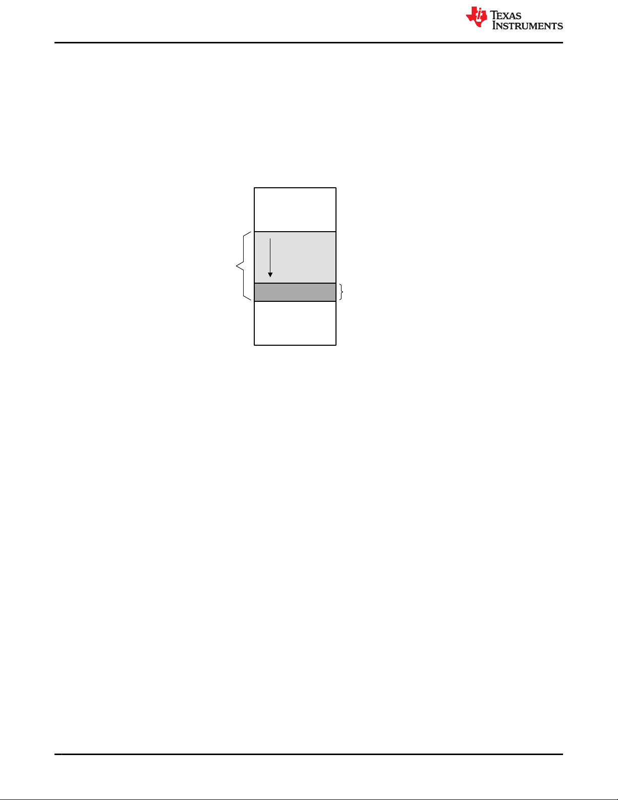
Stack grows
Towards
higher
Memory
addresses
Data Memory
Region of
memory
occupied by
the stack
Monitor for data writes
near the end of the stack
Brief Description of Diagnostics
www.ti.com
6.2.6 Stack Overflow Detection
A stack overflow in a safety application may result in a catastrophic software crash due to data corruption,
lost return addresses, or both. Hence, it is important to detect an impending stack overflow. The enhanced
bus comparator (EBC) unit in ERAD module can monitor the internal address and data buses, and triggers the
RTOSINT interrupt when a specified bus and mask matches a specified value. Hence, the basic approach for
detecting stack overflow will be to configure the EBC unit to trigger an interrupt when the data write address
bus falls within some range prior to the end of a stack. This is illustrated in Figure 6-1. Since this memory is
reserved for stack usage only, a data write within the specified address range indicates that the stack usage
is approaching its allocated size limit. Detection of an impending stack overflow triggers a maskable interrupt.
Programmed error response and any necessary software requirements are defined by the system integrator.
Figure 6-1. Stack Overflow Monitoring
6.2.7 VCRC Check of Static Memory Contents
The TMS320F28002x MCU device family includes co-processor implementing cyclic redundancy check (CRC)
using standard polynomials. The CRC module can be used to test the integrity of SRAM, Flash, and OTP
contents by calculating a CRC for all memory contents and comparing this value to a previously generated
"golden" CRC. The comparison of results, indication of fault, and fault response are the responsibility of
the software managing the test. The cyclical check applied by the CRC logic provides an inherent level of
self-checking (auto-coverage), which can be considered for application in latent fault diagnostics.
6.2.8 VCRC Auto Coverage
The VCRC diagnostic is based on up to 32-bit polynomial. For a given test, only one code is valid out of 2
32
possibilities. Therefore, if there is a fault in the VCRC logic or associated data path, it is extremely unlikely that
the correct passing code will be generated via the fault.
6.2.9 Embedded Real Time Analysis and Diagnostic (ERAD)
The ERAD module provides system analysis capabilities that can be used to detect faults in CPU and other logic
on MCU by configuring bus comparator units that monitor CPU buses and counter units that count events. This
module which is accessible by the application software, consists of the Enhanced Bus Comparator units and
Benchmark System Event Counter units.
The Enhanced Bus Comparator units are used to monitor various CPU buses and generate events which can
then be further processed or used directly. The activity monitored and detected by these units can be used to
generate breakpoints, watch-points or an interrupt (RTOSINT).
The Benchmark System Event Counter units are used to analyze and profile the system. It can count events
when setup as Event Mode and duration between system events when setup as Duration mode.
After application code sets up the ERAD module, it can work independently and generate RTOSINT interrupt in
case of event match occurs. This module can be used as a continuous online monitor of system events on MCU.
40 Safety Manual for TMS320F28002x SPRUIT5 – APRIL 2021
Copyright © 2021 Texas Instruments Incorporated
Submit Document Feedback
Page 41

www.ti.com
Brief Description of Diagnostics
6.2.10 Inbuilt hardware redundancy in ERAD bus comparator module
The ERAD bus comparator units can be used to monitor CPU buses and ERAD supports such 8 comparator
blocks. The activity monitored and detected by these units can be used to generate breakpoints, watch-points
or an interrupt (RTOSINT). Bus comparator module events from different units can be combined using OR
and AND logics to generate new events as required. The faults in the comparison block can be detected by
configuring two comparator blocks to monitor same set of CPU buses continuously and combine them using OR.
RTOS Interrupt cause can indicate if the interrupt is set in one of the block or both.
6.3 Memory (Flash, SRAM and ROM)
6.3.1 Bit Multiplexing in Flash Memory Array
The flash modules implemented in the TMS320F28002x MCU device family have a bit multiplexing scheme
implemented such that the bits accessed to generate a logical (CPU) word are not physically adjacent. This
scheme helps to reduce the probability of physical multi-bit faults resulting in logical multi-bit faults. Rather, they
manifest as multiple single bit faults. As the SECDED flash ECC can correct a single bit fault and detect double
bit fault in a logical word, this scheme improves the usefulness of the flash ECC diagnostic. Bit multiplexing is a
feature of the flash memory and cannot be modified by the software.
6.3.2 Bit Multiplexing in SRAM Memory Array
The SRAM modules implemented in the TMS320F28002x MCU device family have a bit multiplexing scheme
implemented such that the bits accessed to generate a logical (CPU) word are not physically adjacent. This
scheme helps to reduce the probability of physical multi-bit faults resulting in logical multi-bit faults. Rather, they
manifest as multiple single bit faults. The SECDED SRAM ECC diagnostic can correct a single bit fault and
detect double bit fault in a logical word. Similarly, the SRAM parity diagnostic can detect single bit faults. This
scheme improves the usefulness of the SRAM ECC and parity diagnostic. Bit multiplexing is a feature of the
SRAM and cannot be modified by the software.
6.3.3 Data Scrubbing to Detect/Correct Memory Errors
For memories with ECC or Parity, data scrubbing can be used to provide latent fault diagnostic coverage. Bus
masters (CPU or DMA) can be configured to provide dummy reads to the memory (provided a particular bus
master has access to the memory) and the read data can be checked by the built-in ECC or Parity logic. In the
case of SRAMs with ECC protection, single bit errors are corrected and written back. For both SRAMs and flash,
interrupt is issued once the count exceeds the preset threshold in the case of correctable errors and NMI will be
issued in the case of uncorrectable errors.
Since the contents of flash memory are static,Section 6.2.7 provides better diagnostic coverage compared to this
diagnostic.
6.3.4 Flash ECC
The on-chip flash memory is supported by single error correction, double error detection (SECDED) error
correcting code (ECC) diagnostic. In this SECDED scheme, an 8-bit code word is used to store the ECC of 64
bit data and corresponding address. The ECC decoding logic at the flash bank output checks the correctness of
memory content. ECC evaluation is done on every data and program read. The data and program interconnects
that connect the CPU and flash memory is not protected by ECC. Detected correctable errors can be corrected
or not corrected, depending on whether correction functionality is enabled. Single bit address ECC errors are
flagged as uncorrectable errors. Errors that cannot be corrected will generate an NMI and ERRORSTS pin is
asserted. Count of the corrected errors (single bit data errors) is monitored by the flash wrapper and an interrupt
is generated once the count exceeds the programmed threshold. The corrupted memory address of the last error
location is also logged in flash wrapper.
6.3.5 Flash Program Verify and Erase Verify Check
Whenever any program and erase operation is done, the flash controller will perform program and erase verify
check. If the program and erase operation is failed, FSM status register (FMSTAT) will indicate the error by
setting the corresponding flags into the status register.
SPRUIT5 – APRIL 2021
Submit Document Feedback
Safety Manual for TMS320F28002x 41
Copyright © 2021 Texas Instruments Incorporated
Page 42

Brief Description of Diagnostics
www.ti.com
6.3.6 Software Test of ECC Logic
It is possible to test the functionality of the SRAM ECC by injecting single bit and double bit errors in test mode
and performing reads on locations with ECC errors, and checking for the error response. Flash ECC logic can
be checked with the help of ECC test registers (FECC_CTRL, FADDR_TEST, FECC_TEST, FDATAH_TEST,
FDATAL_TEST). Correct functioning of error counter and threshold interrupt associated with single bit errors
can also be verified using this technique. Error response, diagnostic testability, and any necessary software
requirements are defined by the software implemented by the system integrator.
For additional details on implementing this diagnostic for SRAM and FLASH memory, see the Application
Test Hooks for Error Detection and Correction and SECDED Logic Correctness Check sections in the
TMS320F28002x Real-time Microcontrollers Technical Reference Manual.
6.3.7 Software Test of Flash Prefetch, Data Cache and Wait-States
Once enabled, prefetch logic keeps fetching the next 128-bit row (4 x 32-bit words) from flash bank. On detecting
the discontinuity, the prefetch buffer will be cleared. A software test can be performed to ascertain the proper
behavior of this logic. The following sequence of operation can be performed.
1. Disable the prefetch mechanism, enable the timer and Watchdog. Execute a particular function which might
have linear code and code with multiple discontinuities. Store the time “time_1” (timer value) taken for
executing this function.
2. Enable the prefetch mechanism and execute the same function again. Store the time “time_2” (timer value)
taken for executing this function. This value should be less than the time_1 (time_1 > time_2). We can
mark this timer value as a golden value and should expect the same timer values for each run of the same
function.
3. Since each flash bank row has 4 x 32-bit words, number of rows fetched from the flash bank varies as
per the code alignment within the flash bank. Hence, user needs to make sure that the prefetch logic test
function should be aligned/located in particular location within flash to guarantee the same timing behavior
and does not vary compile to compile.
Similar timer-based profiling can be performed to ascertain proper functioning of the data cache and wait states.
6.3.8 Access Protection Mechanism for Memories
All volatile memory blocks including external memories except for M0/M1 have different levels of protection.
This capability allows the user to enable or disable specific access (Fetch, Write) to individual RAM blocks
from individual masters (viz. CPU,DMA). There is no protection for read accesses, therefore, reads are always
allowed from all the masters which have access to that RAM block. To identify conditions when the master
access to an SRAM is blocked, see the device-specific technical reference manual. This configuration can
be changed during run-time and allows memory to block access from specific masters or specific application
threads within the same master. This capability helps support freedom from interference requirements required
by some applications.
6.3.9 SRAM ECC
Selected on-chip SRAMs support SECDED ECC diagnostic with separate ECC bits for data and address. For
the specific address ranges that support ECC, see the TMS320F28002x MCU device-specific data sheet. In
SECDED scheme, a 21-bit code word is used to store the ECC data calculated independently for each 16 bit
of data and for address. The ECC logic for the SRAM access is located in the SRAM wrapper. The ECC is
evaluated directly at the memory output and data is sent to CPU after the data integrity check. The data and
address interconnects from SRAM to the CPU is not protected using ECC. Detected correctable errors are
corrected and it is possible to monitor the number of corrected errors. The SRAM wrapper can be configured
to trigger an interrupt once the number of corrected errors crosses a threshold. Uncorrectable SRAM errors
trigger an NMI and the ERRORSTS pin is asserted. The ECC logic for the SRAM is enabled at reset. For more
information regarding memories supporting ECC, see the TMS320F28002x MCU device-specific data sheet.
42 Safety Manual for TMS320F28002x SPRUIT5 – APRIL 2021
Copyright © 2021 Texas Instruments Incorporated
Submit Document Feedback
Page 43

www.ti.com
Brief Description of Diagnostics
6.3.10 SRAM Parity
Selected on-chip SRAMs support parity diagnostic with separate parity bits for data and address. For the specific
address ranges that support parity, see the device-specific data sheet. In the parity scheme, a 3-bit code word
is used to store the parity data calculated independently for each 16 bit of data and for address. The parity
generation and check logic for the SRAM is located in the SRAM wrapper. The parity is checked directly at
the memory output and data is sent to CPU after the data integrity check. The data and address interconnect
from SRAM to the CPU is not protected using parity. SRAM parity errors trigger an NMI and the ERRORSTS is
asserted. The parity logic for the SRAM is enabled at reset. For more information regarding memories supporting
parity, see the TMS320F28002x MCU device-specific data sheet.
6.3.11 Software Test of Parity Logic
It is possible to test the functionality of parity error detection logic by forcing a parity error into the data or
parity memory bits, and observing whether the parity error detection logic reports an error. Parity can also be
calculated manually and compared to the hardware calculated value stored in the parity memory bits.
For additional details on implementing this diagnostic for SRAM, see the Application Test Hooks for Error
Detection and Correction section in TMS320F28002x Real-time Microcontrollers Technical Reference Manual.
6.3.12 Software Test of SRAM
It is possible to test the integrity of SRAM (bit cells, address decoder and sense amplifier logic) using the CPU.
Based on the safety requirement, this test can be performed at start-up or during application time. If the SRAM
contents are static, a CRC check using VCRC can also be performed in place of destructive test (test where
memory contents need to be restored after the test). For details on implementing this particular test, check the
safety package delivered with this specific C2000 MCU device.
6.3.13 Memory Power-On Self-Test (MPOST)
Start-up test of the memories provides detection for permanent faults inside on-chip memories. Some of the
C2000 devices family products supports the Programmable Built in Self-Test (PBIST), an easy and efficient
way of testing the memories by configuring the customer OTP field. PBIST architecture consists of a small
co-processor with a dedicated instruction set targeted specifically toward testing memories. This co-processor
when triggered, executes test routines stored in the PBIST ROM and runs them on multiple on-chip memory
instances. The on-chip memory configuration information is also stored in the PBIST ROM. PBIST provides very
high diagnostic coverage for permanent faults on the implemented SRAMs and ROMs. If PBIST is configured,
test (March13n for SRAMs or triple_read_xor_read for ROMs) is executed on all the memory instances. The
PBIST test status is stored in the on chip memory. The term “memory” covered by PBIST indicates to SRAM and
ROM. Flash testing is not covered as part of this specification.
Since the code for testing of the memories resides in boot rom, it is not be possible to test the boot-rom using
PBIST. Hence a separate boot-rom checksum test will be done prior to PBIST. Prior to performing any test using
PBIST, an always fail test case is executed. This is to validate the proper functioning of the PBIST controller and
its ability to indicate failure. For more details, please refer to C2000 Memory Power-On Self-Test (M-POST).
6.3.14 Background CRC
Background CRC is a non-intrusive CRC calculation module. CRC calculation needs to be kicked off by the
application and it can continue with the regular application execution. Once kicked off, the module will trigger an
interrupt on completion of test or occurance of an error. The module generates memory access which will be
serviced once all pending functional accesses from CPU and DMA are complete. Since the memory accesses
happen only during idle cycles, the MIPS impact of performing CRC computation is zero or very minimal. This
modules helps to cover the faults in memory bit cells, address decoder logic and sense amplifier ( all memory
logic involved during read operation).
SPRUIT5 – APRIL 2021
Submit Document Feedback
Safety Manual for TMS320F28002x 43
Copyright © 2021 Texas Instruments Incorporated
Page 44

Brief Description of Diagnostics
www.ti.com
6.3.15 Watchdog for Background CRC
The CRC module has an embedded windowed watchdog as a diagnostic to check memory test completion
in the expected time window. This feature protects against hardware defects or rogue code which cause the
memory check not to complete in the pre-determined duration. Windowing feature helps detect additional failure
modes in the watchdog operation, (stuck watchdog). Watchdog counter is a 32-bit counter and BGCRC_WDCNT
reflects the watchdog counter value. The lower and upper window settings for the windowed watchdog are set
by configuring BGCRC_WD_MIN and BGCRC_WD_MAX registers respectively. Failure to complete the memory
check operation in the configured time window will generate an interrupt or NMI as per the configuration.
6.4 On-Chip Communication Including Bus-Arbitration
6.4.1 1oo2 Software Voting Using Secondary Free Running Counter
The TIMER module contains three counters that can be used to provide an operating system time base. While
one counter is used as the operating system time base, it is possible to use one of the other counters as a
diagnostic on the first, using periodic check via software of the counter values in the two timers. The CPU Timer2
can be fed with a different clock source and a different prescale configuration can be selected to avoid common
mode errors. Error response, diagnostic testability, and any necessary software requirements are defined by the
software implemented by the system integrator.
6.4.2 DMA Overflow Interrupt
DMA supports latching one additional trigger event. Before DMA services this latched event if additional event
occurs DMA overflow interrupt is generated, such that, the CONTROL_REG.PERINTFLG is set and another
interrupt event occurs. The CONTROL_REG.PERINTFLG being set indicates a previous peripheral event is
latched and has not been serviced by the DMA
6.4.3 Maintaining Interrupt Handler for Unused Interrupts
The TMS320F28002x MCU devices contain a large number of interrupts; a typical application only uses a very
small subset of all the available interrupts. Multiple configurations are possible for the unused interrupts. This
includes disabling of the unused interrupts, enabling the unused interrupts and return to the application in the
interrupt service routine (ISR), and so forth. Receiving of an interrupt not used in the application might be an
early indication of some faulty scenarios within the TMS320F28002x MCU. Hence, it is highly recommended to
enable all the interrupts and configure the ISR to a common routine for logging or error handling.
6.4.4 Power-Up Pre-Operational Security Checks
During the device boot, it goes through various phases as indicated in Figure 4-6. In the pre-operational phase
(before starting the application), the application code is expected to perform a set of checks to ensure correct
initialization of device security which includes checks to confirm correct link pointer settings, CRC lock setting,
correct partitioning of secure RAM blocks and flash sectors (Grab Bits), setting for execute only protection for
secure RAM blocks and Flash sectors, and correct settings for boot configuration. Before starting the execution
of downloaded code user should check the integrity of the code using CRC function. Once pre-operational
checks are successfully completed with expected results, the device can enter the application phase.
6.4.5 Majority Voting and Error Detection of Link Pointer
The link pointer OTP location is not protected by ECC. To provide better security to the customer code
and enable application safety, majority voting and data consistency based error detection is implemented.
The location of the zone select region in OTP is decided based on the value of three 29-bit link pointers
(Zx-LINKPOINTERx) programmed in the OTP of each zone. The final value of the link pointer is resolved in
hardware when a dummy read is issued to all the link pointers by comparing all the three values (bit-wise voting
logic). Any error in the resolution of the final link pointer value will set the Zx_LINKPOINTERERR register.
6.4.6 PIE Double SRAM Hardware Comparison
PIE SRAM address space is duplicated and data is placed in two memories. During a vector fetch, the ePIE
performs a hardware comparison of both vector table outputs. If there is a mismatch between the two vector
tables, the CPU branches to the address in the PIEVERRADDR register and the ePIE sends trip signals to
the PWMs. If the PIEVERRADDR register value has not been set, the default boot ROM handler at address
0x003FFFBE is used.
44 Safety Manual for TMS320F28002x SPRUIT5 – APRIL 2021
Copyright © 2021 Texas Instruments Incorporated
Submit Document Feedback
Page 45

www.ti.com
Brief Description of Diagnostics
6.4.7 PIE Double SRAM Comparison Check
In order to check the PIE double SRAM comparison feature and the fault handling, it is possible to inject
different data to both the SRAMs by waiting to a redundant vector address. The interrupt corresponding to the
mismatched PIE vector in SRAM needs to be triggered by software. Then software needs to verify that CPU
branches to the address in the PIEVERRADDR register and the ePIE sends trip signals to the PWMs. For
details for implementation of this check, see the Vector Address Validity Check section in the TMS320F28002x
Real-time Microcontrollers Technical Reference Manual.
6.4.8 Software Check of X-BAR Flag
X-BAR flag registers are used to flag the inputs of the ePWM and output X-Bars to provide software knowledge
of the input sources which got triggered. This flag registers can be periodically read to ascertain that no ePWM
tripzones, ePWM syncing or GPIO output signaling is missed.
6.4.9 Software Test of ePIE Operation Including Error Tests
A software test for testing the basic functionality as well as failure modes such as continuous interrupts, no
interrupts, and crossover interrupts can be implemented. Such testing can be based on generating the interrupts
from the peripherals and ensuring that the interrupt is serviced and serviced in proper order. The interrupt can
be generated using either software force capability, for example, ECAP_REGS.ECFRC.CTROVF or creating
the interrupt scenario functionally, for example, creating a counter overflow condition in eCAP. Error response,
diagnostic testability, and any necessary software requirements are defined by the software implemented by the
system integrator.
6.4.10 Disabling of Unused DMA Trigger Sources
Unintended trigger of DMA transfers could corrupt critical data and that could be a potential source of
interference to safety critical applications. In order to avoid the initiation of unintended DMA transfers, it is
recommended that unused DMA channels and DMA trigger sources are disabled at source or by configuring
DMACHSRCSELx registers.
6.4.11 Software Test of CLB Function Including Error Tests
A software test can be utilized to test basic functionality of CLB and to inject diagnostic errors and check for
proper error response. Such a test can be executed periodically. Software requirements necessary are defined
by the software implemented by the system integrator.
6.4.12 Monitoring of CLB by eCAP or eQEP
The Configurable Logic Block (CLB) outputs can be monitored for proper operation by eCAP or eQEP using
internal connections. User should configure CLB to generate a known good sequence of pulses (triggers) as
required by the modules (eCAP or eQEP) to observe outputs through these blocks. The efficiency of monitoring
would be based on customer configuration.
6.4.13 Periodic Software Read Back of SPI Buffer
Using the CLB to SPI interface, without the CPU intervention, CLB will be able to send out a continuous stream
of 16-bit data to SPI which then be saved in the device memory using the FIFO and DMA mechanism of the SPI.
In order to ensure that the data from CLB is reaching to SPI and then to device memory, it is recommended for
the software to implement tests to read back the SPI FIFO contents as well as to read back the final Memory
contents and ensure that they are same.
6.4.14 Timeout detection through ERAD counter
ERAD can monitor the nRDY pin of HIC and give a timeout interrupt based on the configured number of cycles.
When nRDY is low for more than expected cycles, ERAD generates a timeout interrupt to master.
SPRUIT5 – APRIL 2021
Submit Document Feedback
Safety Manual for TMS320F28002x 45
Copyright © 2021 Texas Instruments Incorporated
Page 46

TZ Event
GPIO Logic
(Inverts one signal)
Input X-BAR
DC Event
EPWM2B
EPWM1A
!EPWM2B
TZ1
TZ2
TZ1 & !TZ2
EPWM1A & !(!EPWM2B)
DC Event
GPIO Logic
(Inverts one signal)
Input X-BAR
EPWM1A
EPWM2B
TZ1 & !TZ2
EPWM1A & !(!EPWM2B)
!EPWM2B
EPWM1A
TZ1
TZ2
Brief Description of Diagnostics
www.ti.com
6.5 Digital I/O
6.5.1 eCAP Application Level Safety Mechanism
eCAP module outputs can be checked for saturation, zero width or out of range based on the application
requirement. While measuring the speed of rotating machinery, the application can set bounds on the measured
speed based on the operating profile. Similar bound settings are possible for other application scenarios like
period and duty cycle measurement, decoding current or voltage from the duty cycle of the encoded current
or voltage sensors, and so forth. Online monitoring of periodic interrupts can also be performed for improved
diagnostic coverage based on the application profile.
6.5.2 ePWM Application Level Safety Mechanism
ePWM is typically used as the output signal in closed loop control applications such as EV traction, DC-DC and
industrial drive. In such applications, the failure in ePWM output, such as stuck-at fault or frequency or duty
cycle change, will result in disturbance to control loop parameters or variables, leading to conditions such as
over voltage, over current or over temperature. By monitoring characteristics of these control loop parameters
implemented at application-level, faults in the ePWM module can be detected.
6.5.3 ePWM Fault Detection Using X-BAR
A combination of ePWM outputs feedback to input X-BAR, GPIO inversion logic and Digital Compare (DC)
sub-module of ePWM can be used for implementing simple (for example, signal cross over) but effective
anomaly checks on the PWM outputs. The feature can be used to trip the PWM and enter safe state if any
anomaly is detected.
Figure 6-2. ePWM Fault Detection Using X-BAR
6.5.4 ePWM Synchronization Check
ePWM modules can be chained together via a clock synchronization scheme that allows them to operate
as a single system when required. In the synchronous mode of operation, it is critical to check the proper
synchronization of the various PWM instances to avoid catastrophic conditions. The synchronization of the
various PWMs can be checked by reading the TBSTS.SYNCI bit of ePWM module. The proper phase
relationship intended as a result of the sync operation can be cross-checked by comparing the TBCTR register
value.
6.5.5 eQEP Application Level Safety Mechanism
eQEP is typically used in closed loop control applications to have direct interface with a linear or rotary
incremental encoder to get position, direction, and speed information from a rotating machine for use in highperformance motion and position-control system. In such applications, it is possible to monitor eQEP outputs for
saturation, zero value or out of range based on the application requirement. While estimating the speed/position
of rotating machinery, the application can set bounds on the measured speed/position based on the operating
profile. Online monitoring of periodic interrupts from eQEP can also be performed for improved diagnostic
coverage based on the application profile.
46 Safety Manual for TMS320F28002x SPRUIT5 – APRIL 2021
Copyright © 2021 Texas Instruments Incorporated
Submit Document Feedback
Page 47

www.ti.com
Brief Description of Diagnostics
6.5.6 eQEP Quadrature Watchdog
eQEP peripheral contains a 16-bit watchdog timer that monitors the quadrature-clock to indicate proper
operation of the motion-control system. The eQEP watchdog timer is clocked from SYSCLKOUT/64 and the
quadrate clock event (pulse) resets the watchdog timer. If no quadrature-clock event is detected until a period
match, then the watchdog timer will time out and the watchdog interrupt flag will be set. The timeout value is
programmable through the watchdog period register.
6.5.7 eQEP Software Test of Quadrature Watchdog Functionality
A software test can be used to test for basic functionality of the quadrature watchdog as well as to inject
diagnostic errors and check for proper error response. Such a test can be executed at boot or periodically.
Software requirements necessary are defined by the software implemented by the system integrator.
6.5.8 Hardware Redundancy
Hardware redundancy techniques can be applied via hardware or as a combination of hardware and software
to provide runtime diagnostic. In this implementation, redundant hardware resources are utilized to provide
diagnostic coverage for elements within and outside (wiring harness, connectors, transceiver) TMS320F28002x
MCU.
In case of peripherals like GPIO, X-BAR, ePWM, OTTO, DAC, CMPSS, XINT and so forth, hardware
redundancy can be implemented by having multi-channel parallel outputs (where independent outputs are used
for transmitting information, and failure detection is carried out via internal or external comparators) or input
comparison or voting (comparison of independent inputs to ensure compliance with a defined tolerance range on
time and value). In such scenarios, the system can be designed such that the failure of one input/output does not
cause the system to go into a dangerous state. While servicing the error conditions (redundancy conditions) as
in two redundant sources tripping the PWM, always read-back the status flags and ensure that both sources are
active while tripping and thus providing latent fault coverage for the trip logic.
In case of peripherals like ADC, eCAP, HRCAP, eQEP and so forth, hardware redundancy may be implemented
by having multiple instance of the peripheral sample the same input and simultaneously perform the same
operation followed by cross check of the output values.
In case of communication peripherals like DCAN, SPI, SCI and so forth hardware redundancy during signal
reception can be implemented by having multiple instance of the peripheral receive the same data followed
by comparison to ensure data integrity. Hardware redundancy during transmission can be employed by having
complete redundant signal path (wiring harness, connectors, transceiver) from the transmitter to receiver or by
sampling the transmitted data by a redundant peripheral instance followed by data integrity check.
Hardware Redundancy for device interconnect (INC) can be implemented by simultaneous data storage/
transmission by independent processing units for computation followed by comparison of the computed results.
While implementing hardware redundancy for ADC and DAC modules, additional care needs to be taken to
ensure common cause failures do not impact both instances in same way. Reference voltage sources configured
for redundant module instances should be independent. Additionally, for ADC SOC trigger sources used for
redundant ADC instance should be configured to different ePWM module instance. In case of DAC module the
comparator can be implemented using an external device.
While implementing hardware redundancy for the ePWM module, it is recommended that ePWM module
instance used is part of separate sync chains. This is to avoid common cause failure on sync signal affecting
both the ePWM modules in same way.
While implementing hardware redundancy for GPIO module, it is recommended to use GPIO pins from different
GPIO groups to avoid common cause failures.
SPRUIT5 – APRIL 2021
Submit Document Feedback
Safety Manual for TMS320F28002x 47
Copyright © 2021 Texas Instruments Incorporated
Page 48

Brief Description of Diagnostics
www.ti.com
6.5.9 HRPWM Built-In Self-Check and Diagnostic Capabilities
The micro edge positioner (MEP) logic in HRPWM is capable of placing an edge in one of 255 discrete time
steps. The size of these steps is of the order of 150 ps. For typical MEP step size, see the device-specific data
sheet. The MEP step size varies based on worst-case process parameters, operating temperature, and voltage.
MEP step size increases with decreasing voltage and increasing temperature and decreases with increasing
voltage and decreasing temperature. Applications that use the HRPWM feature should use the TI-supplied MEP
scale factor optimization (SFO) software function. The SFO function helps to dynamically determine the number
of MEP steps per EPWMCLK period while the HRPWM is in operation.
The HRPWM module has built in self-check and diagnostic capabilities that can be used to determine the
optimum MEP scale factor value for any operating condition. TI provides a C-callable library containing one
SFO function that utilizes this hardware and determines the optimum MEP scale factor. For a given System
Clock frequency at a given temperature, a known MEP scale factor value is returned by the SFO determination
function. Proper System Clock frequency operation is verified by comparing the MEP scale factor value returned
with the expected value.
6.5.10 Information Redundancy Techniques
Information redundancy techniques can be applied via software as an additional runtime diagnostic. In order
to provide diagnostic coverage for network elements outside the TMS320F28002x MCU (wiring harness,
connectors, transceiver) end-to-end safety mechanisms are applied. These mechanisms can also provide
diagnostic coverage inside the TMS320F28002x MCU.
In the case of processing elements (CPU), this refers to multiple executions of the code and software based
cross checking to ensure correctness. The multiple execution and result comparison may be based on either
the same code executed multiple times or diversified software code implemented. For details regarding the
implementation, see the ISO 26262-5:2018, D.2.5.6.
In the case of the DMA, information redundancy techniques refers to additional information besides the data
payload which ensures data integrity. For example, SECDED codes, parity codes, CRCs, etc. enable information
redundancy.
Typical control applications involve measuring three phase the voltage and current. These values are either
sampled directly using the on chip ADC or send to the TMS320F28002x MCU by the sensors which are captured
using eCAP, and so forth. In such scenarios, the correlation between input signals can be used to check the
integrity (for example, if the three phase voltage, V1, V2, V3 is being measured, the function V1 + V2 + V3 = 0 can
be used to provide diagnostic coverage for input signal integrity).
In the case of SRAM and flash memory, critical data, program, variables, and so forth can be stored redundantly
and compared before it is getting used. Care should be taken to avoid compiler optimizing code containing
redundant data/programs. Safety program in flash can be copied to SRAM and execute after performing a CRC
check against a pre-calculated golden CRC value.
6.5.11 Monitoring of ePWM by eCAP
The ePWM outputs can be monitored for proper operation by an input capture peripheral, such as the eCAP.
The connection between ePWM output and eCAP input can be made either externally in the board or internally
using X-BAR. Error response, diagnostic testability, and any necessary software requirements are defined by the
software implemented by the system integrator. Similarly eCAP can be tested by periodically measuring ePWM
pulse width when used as diagnostic for ePWM. XINTxCTR (counter of XINT module), capture mode of eQEP
and DCCAP (PWM event filter unit) can also be used to detect rising/falling edges of the PWM and extract the
timestamping information. This information can be further used to build additional diagnostics.
48 Safety Manual for TMS320F28002x SPRUIT5 – APRIL 2021
Copyright © 2021 Texas Instruments Incorporated
Submit Document Feedback
Page 49
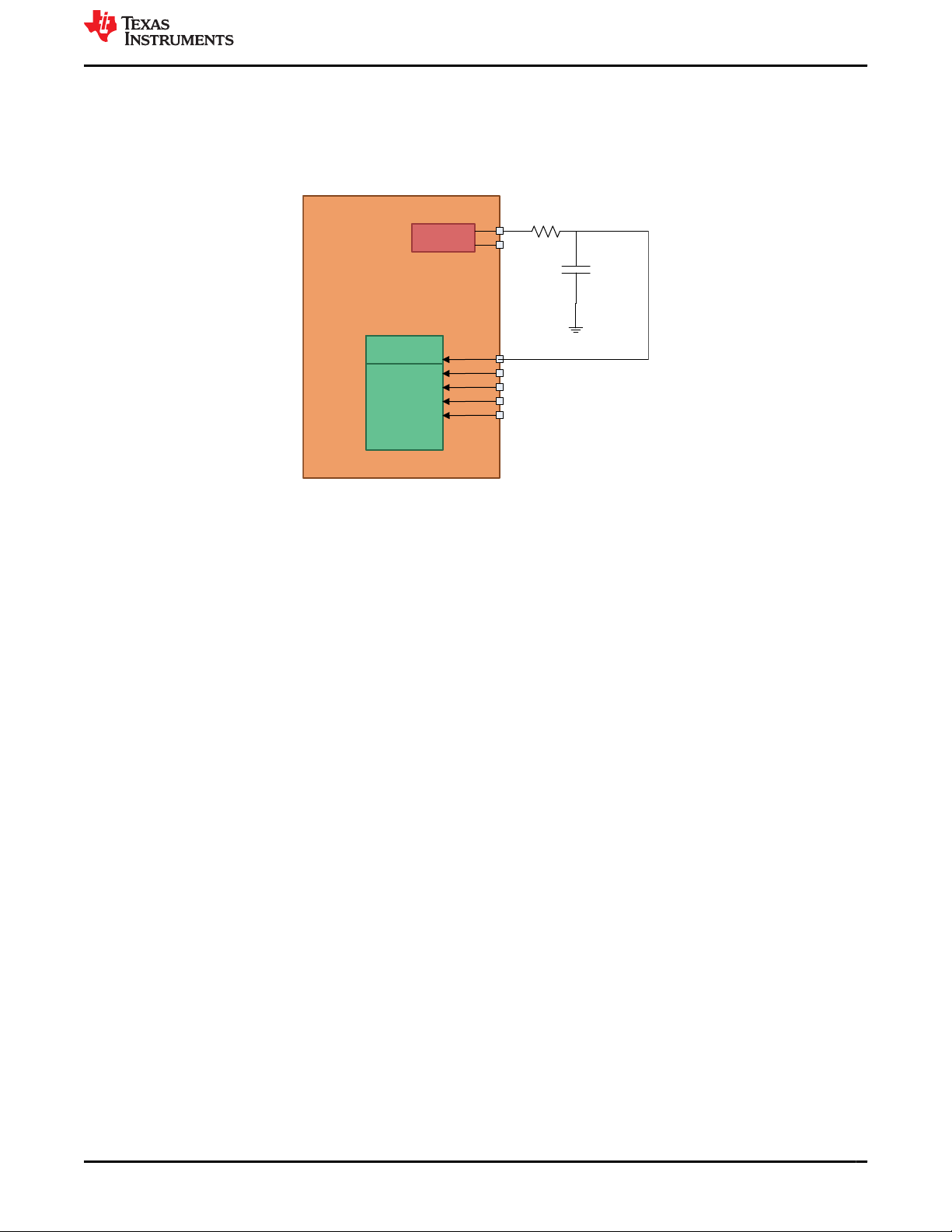
ADC
PWM1
B
A
A0
A1
A2
A3
A4
www.ti.com
Brief Description of Diagnostics
6.5.12 Monitoring of ePWM by ADC
The ePWM outputs can be monitored for proper operation by ADC using a board level feedback as indicated in
Figure 6-3. The technical details for implementing such a loopback like signal resolution, and so forth is provided
in the link [9]. Error response, diagnostic testability, and any necessary software requirements are defined by the
software implemented by the system integrator.
Figure 6-3. Monitoring of ePWM by ADC
6.5.13 Online Monitoring of Periodic Interrupts and Events
For interrupts and events, failures can be detected using information about the time behavior of the system. The
monitored signals can be either periodic or aperiodic.
For a typical closed loop control application, most of the critical events are periodic in nature and these periodic
events can be monitored and incoherence in the events can be used for fault detection. A few places where
online monitoring periodic interrupts and events can be employed include:
• Online monitoring of periodic occurrence of interrupts, for example, ePWM, ADC end-of-conversion (EOC),
eCAP and eQEP interrupts
• Online monitoring of periodic events:
– Periodic generation of ADC start-of-conversion (SOC): ADC SOC signal can be used to generate an
external interrupt (XINT) with the help of X-BAR. The occurrence of periodic interrupts can be monitored.
– Periodic DMA trigger: Some of the DMA events may also be periodic in nature (for example, copy of ADC
results, updating of CMPA register, and so forth). DMA supports interrupt generation on the completion of
the DMA action and this capability can be used for online monitoring.
Monitoring of interrupts and events which are normally not expected during the correct operation can also be
used to improve the diagnostic coverage (ECC correctable error interrupt).
6.5.14 SD Modulator Clock Fail Detection Mechanism
When SD modulator clock fails or goes missing for 256 continuous system clock cycles, clock fail detection
sub-module in the input control unit of SD modulator detects the failure and generates an interrupt to CPU. This
mechanism can be used to detect missing modulator clock faults or any faults in digital I/O connecting modulator
clock.
6.5.15 Software Test of Function Including Error Tests
A software test can be utilized to test basic functionality of the module and to inject diagnostic errors and check
for proper error response. Such a test can be executed at boot or periodically. Software requirements necessary
are defined by the software implemented by the system integrator.
SPRUIT5 – APRIL 2021
Submit Document Feedback
Safety Manual for TMS320F28002x 49
Copyright © 2021 Texas Instruments Incorporated
Page 50

Brief Description of Diagnostics
www.ti.com
Ideas for creating some module specific tests functionality and error tests are given below:
• DMA functionality can be checked by transferring a known good data from a source memory to the
destination memory and checking for data integrity after the transfer. The transfer can be initiated using the
software trigger available (CONTROL.PERINTFRC). On chip timer can be used to profile the time required
for such a data transfer.
• Software test of input and output X-BAR module can be performed by having a loop created (output X-BAR
can be used as stimulus to input X-BAR) using the input and output X-BAR, sending a known test sequence
at the input and observing it at the final output. Integrity of ePWM X-BAR can be checked by sending the test
stimulus and observing the response using ePWM trip or sync functionality.
• Software test of XINT functionality can be checked by configuring the input X-BAR and forcing the
corresponding GPIO register to generate an interrupt. The diagnostic coverage can be enhanced by
performing checks for the polarity (XINTxCR.POLARITY) and enable (XINTxCR.ENABLE) functionality as
well.
• eCAP, HRCAP and eQEP functionality can be checked by looping back the PWM, HRPWM or GPIO outputs
to the respective module inputs, providing a known good sequence as required by the module and observing
the module output. In the case of eCAP and HRCAP, the test can be done internally with the help of input
X-BAR.
• ROM prefetch functionality can be checked using similar techniques as given in Section 6.3.7.
• The ePWM module consists of Time-Base (TB), Counter Compare (CC), Action Qualifier (AQ), Dead-Band
Generator (DB), PWM Chopper (PC), Trip Zone (TZ), Event Trigger (ET) and Digital Compare (DC)
sub-modules. The individual sub-modules can be tested by providing suitable stimulus using ePWM and
observing the response using one of the capture (time stamping) modules (eCAP, XINT, eQEP, and so
forth). It is recommended to cover the various register values associated with application configuration while
performing the software test. Due to the regular linear nature of the various sub-modules, it is possible to get
high coverage using a software test.
• A software test of SRAM wrapper logic should provide diagnostic coverage for arbitration between various
masters having access to the particular SRAM and correct functioning of access protection. This is in addition
to the test used to provide coverage of SRAM bit cells (see Section 6.3.12).
• The interconnect (INC) functionality can be tested by writing complementary data-patterns like
0xA5A5,0x5A5A, and so forth from processing units from CPU, and reading back it from registers of the
IPs’ connected via different bridges. The read-back data can be compared with expected golden values
to ensure fault-free interconnect operation. This exercise can be repeated for different data width types of
accesses (16 and 32 bits) and wide address ranges as applicable. The CPU accesses can be repeated for
different instances of peripherals used in application connected to various bridges as shown in Figure 4-1.
• DAC has a set of control registers that can be checked by writing complementary data-patterns like 0xA5A5,
0x5A5A, and so forth in 16-bit access mode. All the registers can be read back and compared to expected
values. Registers can be checked for reset feature by configuring the registers to 0xA5A5 pattern, asserting
soft reset of DAC, reading back the registers and comparing the read back value with the expected reset
value. Lock register can be checked to ensure it is set-once. Also, the registers which are getting locked must
not update when written. To test core functionality of the DAC module, it can be configured using software to
provide a set of predetermined voltage levels. These voltage levels can be measured by external or internal
ADC and results thus obtained can be cross checked against the expected value to ensure proper operation.
Extreme corner values of DAC as per application can be programmed and tested to check the successful
conversion of digital to analog module across a valid range.
• Comparator sub-system (CMPSS) has a set of registers which can be checked by writing complementary
data-patterns like 0xA5A5, 0x5A5A, and so forth in both 16 and 32 bit access modes. These can be read
back and compared against expected values. These accesses can be covered by applicable masters viz.
DMA and CPU. Features of the CMPSS module such as ramp decrement can be checked for counting
down of RAMPDLYA after it is loaded from RAMPDLYS by a rising PWMSYNC signal. It should be ensured
that the decrementer reduces to zero and stays there until next reload from RAMPDLYS. Extreme values
of RAMPDLYS can be configured before count down. Digital filter CTRIPHFILCTL/CTRIPLFILCTL registers
can be checked by configuring them to a variety of SAMPWIN (Sample window) and THRESH (Majority
voting threshold) values, and then verifying COMPHSTS/COMPLSTS changes with change in filter output.
Applicable range of filter clock pre-scaler values (CTRIPLFILCLKCTL) can be exercised to ensure that filter
samples correctly.
50 Safety Manual for TMS320F28002x SPRUIT5 – APRIL 2021
Copyright © 2021 Texas Instruments Incorporated
Submit Document Feedback
Page 51
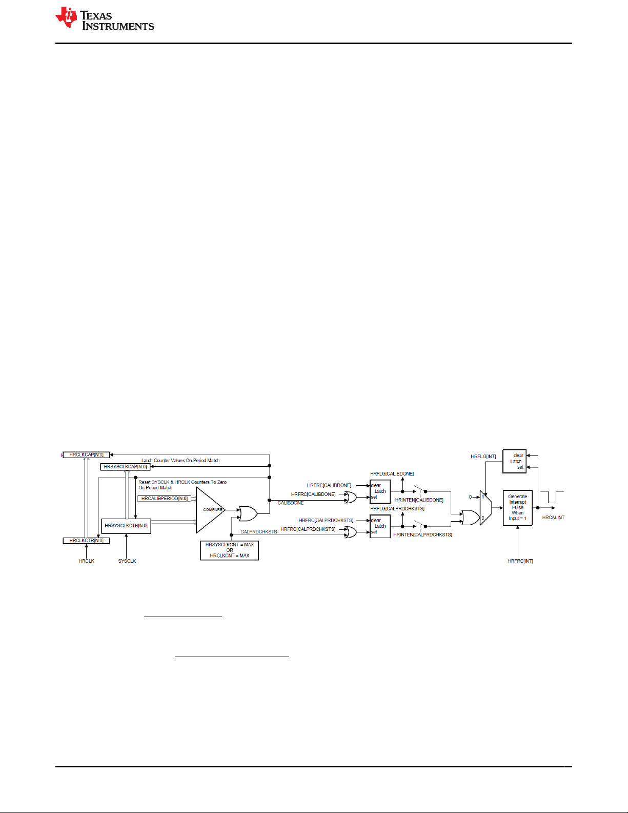
HRSYSCLKCAP
HRCLKCAP
* Pr
128
u
RawCount scaleFactor
Measurement ns SysClk d ns
www.ti.com Brief Description of Diagnostics
• The general operation of the CPU Timers can be tested by a software test by loading 32-bit counter register
TIMH from period register PRDH, starts decrementing of the counter on every clock cycle. When counter
reaches zero a timer interrupt output generates an interrupt pulse. While testing the timer functionality vary
the Timer Prescale Counter (TPR) value and also vary input clocks by selecting clock source as SYSCLK,
INTOSC1, INTOSC2, or XTAL. Test interrupts generation capability at the end of the timer counting. Check
for the time overflow flag and Timer reload (TRB) functions in TCR register for correct functioning.
• A software test function in DCSM can be implemented independently in zone1, zone2 and unsecured zone
to check DCSM functionality. Device security configurations are loaded from OTP to DCSM during the device
boot phase. The test function can implement access filtering checks (read-write and execute permissions) to
RAMs and flash sectors belonging to the same zone and different zone. An additional check for EXEONLY
configuration can also be implemented for the RAMs and flash sectors to ensure that all access other than
execute access is blocked.
6.5.16 Monitoring of HRPWM by HRCAP
The HRPWM outputs can be monitored for proper operation by an input capture peripheral, such as the HRCAP.
The connection between HRPWM output and HRCAP input can be made either externally in the board or
internally using X-BAR. Error response, diagnostic testability, and any necessary software requirements are
defined by the software implemented by the system integrator. Similarly HRCAP can be tested by periodically
measuring HRPWM pulse width when used as diagnostic for HRPWM. XINTxCTR (counter of XINT module),
capture mode of eQEP and DCCAP (PWM event filter unit) can also be used to detect rising/falling edges of
the PWM and extract the timestamping information. This information can be further used to build additional
diagnostics.
6.5.17 HRCAP Calibration Logic Test Feature
The calibration logic consists of two free-running counters; one clocked by HRCLK(HRCLKCTR) and the other
clocked by SYSCLK(HRSYSCLKCTR). When HRSYSCLKCTR is equal to HRCALIBPERIOD, the calibration
block will capture and reset both counter values, then trigger an interrupt indicating a new scale factor is ready to
be calculated. The scale factor can be found by dividing HRSYSCLKCAP by HRCLKCAP, see Equation 1. This
scale factor computation should be done inside of the calibration interrupt service routine. After computing scale
factor, Equation 2 can be applied to get actual measurement of captured value from raw count.
The full details of the calibration block are described in Figure 6-4.
Figure 6-4. HRCAP Calibration
(1)
SPRUIT5 – APRIL 2021
Submit Document Feedback
Copyright © 2021 Texas Instruments Incorporated
(2)
Safety Manual for TMS320F28002x 51
Page 52
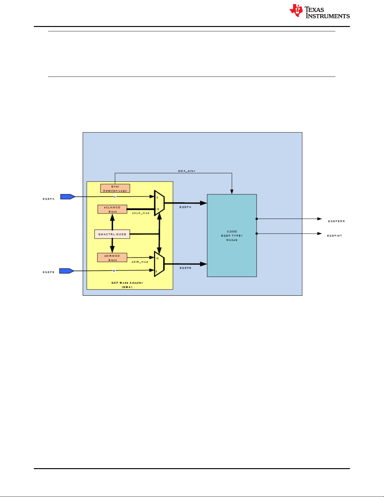
Brief Description of Diagnostics
www.ti.com
Note
Even with calibration, noise on the 1.2 V VDD supply will negatively affect the standard deviation of
the HRCAP sub-module. Care should be taken to ensure that the 1.2 V supply is clean, and that
noisy internal events such as enabling and disabling clock trees have been minimized while using the
HRCAP.
6.5.18 QMA Error Detection Logic
The QEP Mode Adapter (QMA) is designed to extend the C2000 eQEP module capabilities to support the
additional modes described in QMA Module section in the TMS320F28002x Real-time Microcontrollers Technical
Reference Manual. The QMA module has error detection logic to detect illegal transitions on EQEPA and
EQEPB input signals. The QMA module’s error and interrupt are integrated inside the eQEP module.
Figure 6-5. QMA Module Block Diagram
6.6 Analog I/O
6.6.1 ADC Information Redundancy Techniques
Information redundancy techniques can be applied via software for providing runtime diagnostic coverage on
ADC conversions. Time redundancy technique can be applied where multiple conversions on same ADC
followed by comparison of results done in software. In addition, the correlation between input signals can be
used to check the integrity (for example, if the three phase voltage, V1, V2, V3 is being measured using ADC,
the function V1 + V2 + V3 = 0 can be used to provide diagnostic coverage for input signal integrity and ADC
conversion).
Error response, diagnostic testability, and any necessary software requirements are defined by the software
implemented by the system integrator.
6.6.2 ADC Input Signal Integrity Check
ADC input signal integrity can be checked using a mix of hardware and software runtime diagnostic on ADC
conversions. Filtering or plausibility check (value fall in an expected range) of the converted values can be
performed using some of the built in hardware mechanisms available within the device. Plausibility check of the
input signal can be checked with the help of comparator by setting the proper high and low threshold values. The
plausibility check of converted results can be checked by using ADC Post Processing Block.
52 Safety Manual for TMS320F28002x SPRUIT5 – APRIL 2021
Copyright © 2021 Texas Instruments Incorporated
Submit Document Feedback
Page 53
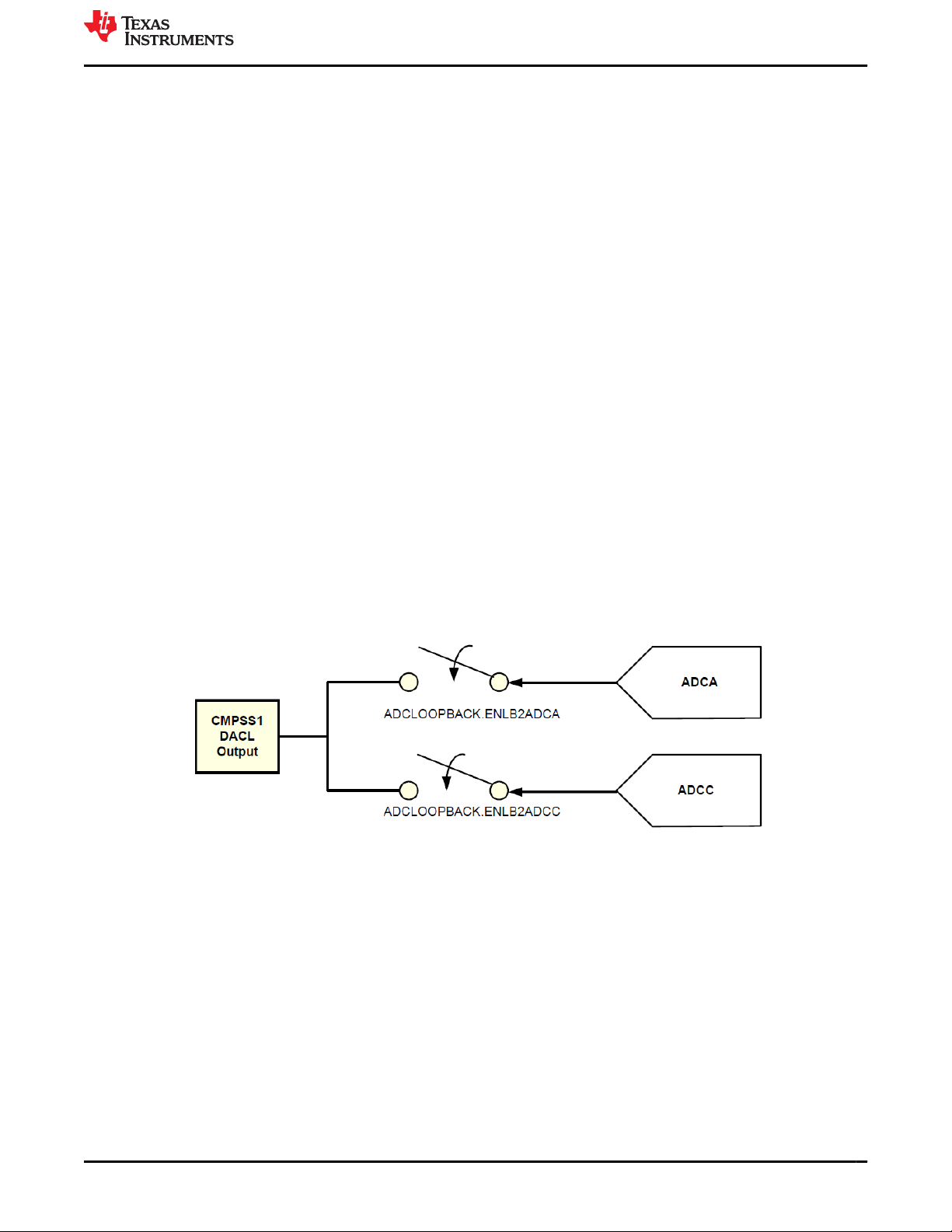
www.ti.com
Brief Description of Diagnostics
6.6.3 ADC Signal Quality Check by Varying Acquisition Window
External signal sources vary in their ability to drive an analog signal quickly and effectively. In order to achieve
rated resolution, the signal source needs to charge the sampling capacitor in the ADC core to within 0.5 LSBs of
the signal voltage. The acquisition window is the amount of time the sampling capacitor is allowed to charge and
is configurable for SOCx by the ADCSOCxCTL.ACQPS register. This configurable parameter can also be used
to provide diagnostic coverage for the input signal path and ADC sampling capacitor logic. The test can be done
by redundant conversion of the same input signal by ADC using the preset ACQPS configuration and an ACQPS
configuration higher than the preset configuration. The results thus obtained have to be within a pre-defined
range determined by the application and ADC specification parameters.
6.6.4 CMPSS Ramp Generator Functionality Check
CMPSS ramp generation functionality is used in certain control applications (peak current mode control).
The functionality of ramp generator can be checked by reading back the contents of DACHVALA register
and ensuring that the register value is periodically updated based on the RAMPDLY, RAMPDECVAL and
RAMPMAXREF. Error response, diagnostic testability, and any necessary software requirements are defined by
the software implemented by the system integrator.
6.6.5 DAC to ADC Loopback Check
Integrity of ADC can be checked monitoring DAC output using ADC. DAC in CMPSS can be configured using
software to provide a set of predetermined voltage levels. These voltage levels can be measured by the ADC
and results thus obtained can be cross checked against the expected value to ensure proper functioning of ADC.
This technique can be applied during run time as well to ensure that proper voltage levels are being driven from
CMPSS DAC.
For more information on the CMPSS DAC channels that can be sampled by ADC without external board
level connections, see the device-specific data sheet or technical reference manual. ADCDACLOOPBACK
register n CMPSS module needs to be configured to enable this mode. To avoid common cause failures, it
is recommended to keep the references voltages of the ADC and DAC different while performing the test. In
addition, the input signal to ADC should not be driven by any other sources while the test is being performed.
Figure 6-6. DAC to ADC Loopback
SPRUIT5 – APRIL 2021
Submit Document Feedback
Safety Manual for TMS320F28002x 53
Copyright © 2021 Texas Instruments Incorporated
Page 54
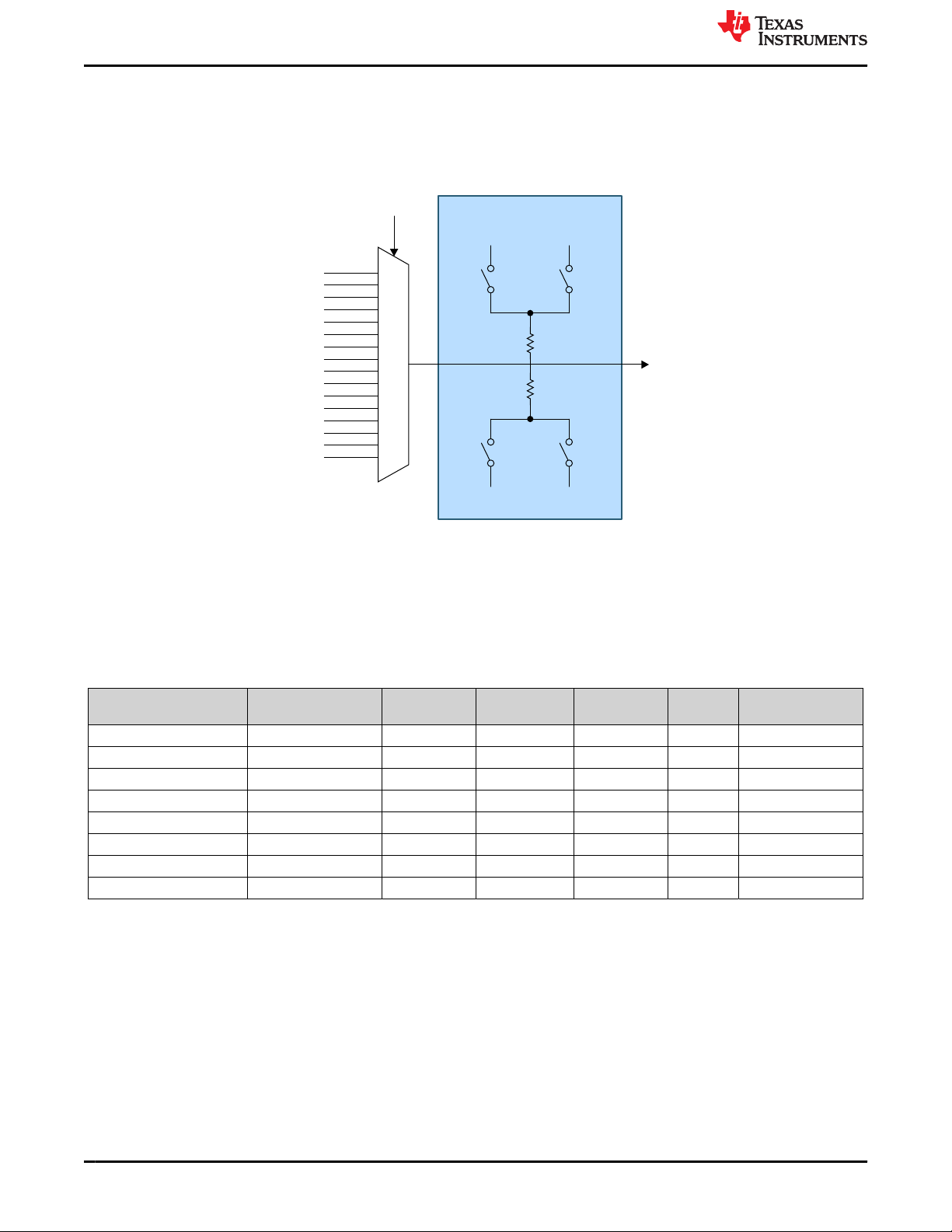
CHSEL
0
ADCIN0
1
ADCIN1
2
ADCIN2
3
ADCIN3
4
ADCIN4
5
ADCIN5
6
ADCIN6
7
ADCIN7
8
ADCIN8
9
ADCIN9
10
ADCIN10
11
ADCIN11
ADCIN12
12
13
ADCIN13
14
ADCIN014
15
ADCIN15
S2
VDDA
S1
VSSA
Opens/Shorts Detection Circuit
S3
VDDA
S4
VSSA
5 kW
7 kW
To S+H
Brief Description of Diagnostics
www.ti.com
6.6.6 Opens/Shorts Detection Circuit for ADC
The opens/shorts detection circuit (OSDETECT) can be used to detect ADC input channel faults in the system.
The circuit connects to the ADC input after the channel select multiplexer but before the S+H circuit as shown
in Figure 6-7. Error response, diagnostic testability, and any necessary software requirements are defined by the
software implemented by the system integrator.
Figure 6-7. ADC Open-Shorts Detection Circuit
The circuit can be operated by writing a value to the DETECTCFG field in the ADCOSDETECT register. This will
cause the circuit to source a voltage onto the input during the S+H phase of any conversion. The voltage and
drive strength of the OSDETECT circuit for different DETECTCFG settings is given in Table 6-1. For additional
details on implementing this diagnostic, see the Opens/Shorts Detection Circuit (OSDETECT) section in the
TMS320F28002x Real-time Microcontrollers Technical Reference Manual.
Table 6-1. ADC Open-Shorts Detection Circuit Truth Table
ADCOSDETECT.DETECT
CFG
0 Off Open Open Open Open Open
1 Zero Scale Closed Open Open Closed 5K || 7K
2 Full Scale Open Closed Closed Open 5K || 7K
3 5/12 VDDA Open Closed Open Closed 5K || 7K
4 7/12 VDDA Closed Open Closed Open 5K || 7K
5 Zero Scale Open Open Open Closed 5K
6 Full Scale Open Open Closed Open 5K
7 Zero Scale Closed Open Open Open 7K
6.6.7 VDAC Conversion by ADC
Reference voltage input to COMPDACs (VDAC) is double bonded with ADCB input. For detecting faults in
VDAC supply and corresponding analog I/O, it can be converted by ADC. The ADC result output can be cross
checked against the expected output to identify any faults. Programmed error response and any necessary
software requirements are defined by the system integrator.
54 Safety Manual for TMS320F28002x SPRUIT5 – APRIL 2021
Source Voltage S4 S3 S2 S1 Drive Impedance
Submit Document Feedback
Copyright © 2021 Texas Instruments Incorporated
Page 55

www.ti.com
Brief Description of Diagnostics
6.6.8 Disabling Unused Sources of SOC Inputs to ADC
ADC SOC (start of conversion) signal input to ADC module can be triggered by multiple sources, include
software, CPU Timers, GPIO, and ePWM module instances, and so forth. In order to achieve freedom from
interference due to a fault originating from an peripheral not used in implementing the safety function and
cascading into ADC, it is recommended that application configures only the requires SOC triggers. This is a way
to avoid faults originating from an outside source to impact functionality of ADC.
6.7 Data Transmission
6.7.1 Information Redundancy Techniques Including End-to-End Safing
Information redundancy techniques can be applied via software as an additional runtime diagnostic. There are
many techniques that can be applied, such as read back of written values and multiple reads of the same target
data with comparison of results.
In order to provide diagnostic coverage for network elements outside the TMS320F28002x MCU (wiring harness,
connectors, transceiver), end-to-end safety mechanisms are applied. These mechanisms can also provide
diagnostic coverage inside the TMS320F28002x MCU. There are many different schemes applied, such as
additional message checksums, redundant transmissions, time diversity in transmissions, and so forth. Most
commonly checksums are added to the payload section of a transmission to ensure the correctness of a
transmission. These checksums, sequence counter and timeout expectation (or time stamp) are applied in
addition to any protocol level parity and checksums. As these are generated and evaluated by the software at
either end of the communication, the whole communication path is safed, resulting in end-to-end safing.
Any end-to-end communications diagnostics implemented should consider the failure modes and potential
mitigating safety measures described in IEC 61784-3:2016 and summarized in IEC 61784-3:2016, Table 1.
6.7.2 Bit Error Detection
When the CAN module transmits information onto its bus, it can also monitor the bus to ensure that the
transmitted information is appearing as expected on the bus. If the expected values are not read back from
the bus, the hardware can flag the error and signal an interrupt to the CPU. This feature must be enabled and
configured in software.
LIN module supports detection of bit error condition. An error flag bit is set when there has been a bit error
detected by the bit monitor in TED (TXRX Error Detector sub-module). A bit error indicates that a collision has
happened on the LIN bus, for example, the bit value that is monitored is different from the bit value that is sent.
When bit error is detected the transmission is aborted no later than the next byte
6.7.3 CRC in Message
The CAN module appends a CRC word along with the message. The CRC values are calculated and transmitted
by the transmitter, and then re-calculated by the receiver. If the CRC value calculated by the receiver does not
match the transmitted CRC value, a CRC error will be flagged. Error response and any necessary software
requirements are defined by the system integrator.
6.7.4 DCAN Acknowledge Error Detection
When a node on the CAN network receives a transmitted message, it sends an acknowledgment that it
received the message successfully. When a transmitted message is not acknowledged by the recipient node, the
transmitting DCAN will flag an acknowledge error. Error response and any necessary software requirements are
defined by the system integrator.
6.7.5 DCAN Form Error Detection
Certain types of frames in the DCAN have a fixed format per the CAN protocol. When a receiver receives a bit in
one of these frames that violate the protocol, the module will flag a form error. Error response and any necessary
software requirements are defined by the system integrator.
SPRUIT5 – APRIL 2021
Submit Document Feedback
Safety Manual for TMS320F28002x 55
Copyright © 2021 Texas Instruments Incorporated
Page 56

Brief Description of Diagnostics
www.ti.com
6.7.6 DCAN Stuff Error Detection
In the CAN message protocol, several of the frame segments are coded through bit stuffing. Whenever a
transmitter detects five consecutive bits of identical value in the bit stream to be transmitted, it automatically
inserts a complementary bit into the actual transmitted bit stream. If a 6th consecutive equal bit is detected in
a received segment that should have been coded by bit stuffing, the DCAN module will flag a stuff error. Error
response and any necessary software requirements are defined by the system integrator.
6.7.7 I2C Access Latency Profiling Using On-Chip Timer
Each I2C message takes fixed number of system clock cycles for completing the transaction. The master can
detect the transaction completion based on message acknowledge signaling from the slave. On chip timer
module can be used for profiling the time required for completing each transaction.
6.7.8 I2C Data Acknowledge Check
When a node on the I2C network receives a byte (address or data), it sends an acknowledgment that the
address is acknowledged or the data byte is received successfully. When a transmitted message is not
acknowledged by the recipient I2C, the transmitting I2C will flag NACK. Necessary software requirements are
defined by the system integrator. For example a function which needs to transfer 4 bytes of data and can sent
CRC as 5th byte. The device software can be designed such that the acknowledge is not provided if the data
and CRC doesn’t match.
PMBus supports detection of errors using acknowledgment handshake, which can be configured to work in
either automatic or manual mode(PMBSC.MAN_SLAVE_ACK bit). This acknowledgment handshake can be
effectively implemented by firmware to detect communication faults such as masquerading faults by asserting
NACK if the received address does not equal the slave address or acknowledging every byte received by
PMBus slave receive byte acknowledge, or acknowledging received command byte, and so forth. For more
details, see the UCD3138 Monitoring and Communications Programmer’s Manual.
6.7.9 Parity in Message
This module supports insertion of a parity bit into the data payload of every outgoing message by hardware.
Evaluation of incoming message parity is also supported by hardware. Detected errors generate an interrupt to
the CPU.
6.7.10 SCI Break Error Detection
A SCI break detect condition occurs when the SCIRXD is low for ten bit periods following a missing stop bit. This
action sets the BRKDT flag bit (SCIRXST, bit 5) and initiates an interrupt.
This feature is applicable only when LIN is working in SCI mode. A SCI break detect condition occurs when the
LINRX is low for ten bit periods following a missing stop bit. This action sets the BRKDT flag bit and initiates an
interrupt.
6.7.11 Frame Error Detection
When receiving serial data, each byte of information on the SCI has an expected format. If the received
message does not match this, the SCI hardware can flag an error and generate an interrupt to the CPU. This
feature must be enabled and configured in software.
LIN module supports detection of framing error condition. An error flag bit is set when an expected stop bit
is not found. In SCI compatible mode, only the first stop bit is checked. The missing stop bit indicates that
synchronization with the start bit has been lost and that the character is incorrectly framed. Detection of a
framing error generates an error interrupt if the RXERR INT ENA bit is set. LIN module supports feature to verify
valid Synch Field. It helps in automatic baud rate adjustment by comparing baud rate and adjust if baud rates
differ. If the synch field is not detected within the given tolerances, the inconsistent-synch-field-error (ISFE) flag
will be set and an ISFE interrupt will be generated.
56 Safety Manual for TMS320F28002x SPRUIT5 – APRIL 2021
Copyright © 2021 Texas Instruments Incorporated
Submit Document Feedback
Page 57

www.ti.com
Brief Description of Diagnostics
6.7.12 Overrun Error Detection
If the SCI RX buffer receives new data before the previous data has been read, the existing data will be
overwritten and lost. If this occurs, the SCI hardware can flag the error and generate an interrupt to the CPU.
This feature must be enabled and configured in software.
LIN module supports detection of data overrun condition. An error flag bit is set when the transfer of data from
receive shift register to receiver data buffer register overwrites unread data already in received data register.
Detection of an overrun error also causes the LIN to generate an error interrupt if the SET OE INT bit is one.
6.7.13 Software Test of Function Using I/O Loopback
Most communication modules support digital or analog loopback capabilities for the I/Os. To confirm the
implemented loopback capabilities of the module, see the device-specific technical reference manual. Digital
loopback tests the signal path to the module boundary. Analog loopback tests the signal path from the module
to the I/O cell with output driver enabled. For best results any tests of the functionality should include the I/O
loopback.
6.7.14 SPI Data Overrun Detection
If SPI RX buffer receives new data before the previous data has been read, the existing data will be overwritten
and lost. If this occurs, SPI hardware can flag the error and generate an interrupt to the CPU. This feature must
be enabled and configured in software.
6.7.15 Transmission Redundancy
The information is transferred several times in sequence using the same module instance and compared. When
the same data path is used for duplicate transmissions, transmission redundancy will only by useful for detecting
transient faults. The diagnostic coverage can be improved by sending inverted data during the redundant
transmission.
In order to provide diagnostic coverage of device interconnects and EMIF, read back of written data (in case of
data writes) and multiple read backs of information (in case of data reads) can be employed.
6.7.16 FSI Data Overrun/Underrun Detection
FSI module supports detection of data overrun or underrun conditions.
• Receive buffer Overrun - This event indicates that the transfer of data from receive shift register to receiver
data buffer register overwrites unread data already in received data.
• Receive buffer Underrun – This event indicates that software reads the buffer while it is empty
• Transmit buffer Overrun – This event occurs if a piece of data is overwritten before it has been transmitted.
• Transmit buffer Underrun – This event occurs when the transmitter tries to read data from a location which
has not yet been written.
A flag bit is set and an interrupt is generated when data overrun/underrun error occurs and corresponding
register bit is enabled.
6.7.17 FSI Frame Overrun Detection
FSI module supports detection of frame overrun event. This event indicates that a new frame has been received
while the FRAME_DONE flag was still set. A flag is set and an interrupt is generated if corresponding register bit
is enabled.
6.7.18 FSI CRC Framing Checks
FSI module supports detection of CRC framing error condition. A CRC error will be generated when the received
expected CRC value and the computed CRC value do not match. A flag is set and an interrupt is generated if
enabled.
SPRUIT5 – APRIL 2021
Submit Document Feedback
Safety Manual for TMS320F28002x 57
Copyright © 2021 Texas Instruments Incorporated
Page 58

Brief Description of Diagnostics
www.ti.com
6.7.19 FSI ECC Framing Checks
FSI module supports detection of ECC framing error condition. It supports 16-bit or 32-bit ECC computation
module in both the transmitter and receiver mode. In Transmit mode, software can configure the FSI registers to
compute the ECC value on the data in transmit buffer and include it to be part of the transmit frame in receive
mode. Software can feed the ECC module with received data and ECC value to detect and autocorrect single bit
errors in data, or detect multi-bit errors in received data and invalidate the received data.
Note
ECC check supported in FSI module needs software assistance. The hardware in FSI module
supports ECC computation, but the task of writing data and checking the ECC error has to be handled
in software.
6.7.20 FSI Frame Watchdog
FSI module supports detection of Frame Watchdog Timeout event. This event indicates that the frame watchdog
timer has timed out. The conditions of this timeout are set using the RX_FRAME_WD_CTRL register. As soon
as the start of frame phase is detected, the frame watchdog counter will start counting from 0. The end of frame
phase must complete by the time the watchdog counter reaches the reference value. If this does not happen,
the watchdog will time out and this event will be generated. If this event occurs, the receiver must undergo a soft
reset and subsequent resynchronization in order to guarantee proper operation. When this condition occurs, a
flag is set and an interrupt is generated if enabled.
6.7.21 FSI RX Ping Watchdog
FSI module supports detection of RX Ping Watchdog Timeout event. This event indicates that the ping watchdog
timer has timed out. The receiver has not received a valid frame within the time period specified in the
RX_PING_WD_REF register. The ping frame triggered interrupt is generated when the ping frame has been
triggered and corresponding register bit is enabled. This bit will be set when the ping counter has timed out. An
interrupt is generated if corresponding register bit is enabled. On the transmitter, the ping frame can be set up
and transmitted without any further software or DMA intervention. Ping frames can be transmitted by automatic
ping timer, software, or external triggers.
6.7.22 FSI Tag Monitor
FSI module supports Tag field in the transfer frame. It contains 4-bit FRAME_TAG field of the last successfully
received frame. FSI Tag Monitor checks has to be implemented in software. Tag field for each of the frame
on the receive side can be monitored through software and verified against expected values. In addition to
FRAME_TAG, FSI module supports the user data as fully user-configurable data field, available in data frames.
The user data to be transmitted is set by writing to TX_FRAME_TAG_UDATA.USER_DATA. The received user
data is stored in RX_FRAME_TAG_UDATA.USER_DATA.
6.7.23 FSI Frame Type Error Detection
FSI module supports detection of Frame Type Error. This error indicates that an invalid frame type has been
received. If this error occurs, the receiver must undergo a soft reset and subsequent resynchronization in order
to guarantee proper operation. An interrupt is generated if corresponding register bit is enabled.
6.7.24 FSI End of Frame Error Detection
This error indicates that an invalid end-of-frame bit pattern has been received. If this error occurs, the receiver
must undergo a soft reset and subsequent resynchronization in order to ensure proper operation. An interrupt is
generated if corresponding register bit is enabled.
6.7.25 FSI Register Protection Mechanisms
As a fault avoidance safety measure for key registers of FSI module, registers are protected by EALLOW
privilege, register keys, and a master register lock. These protections ensure that no spurious writes or
unintentional modifications to these registers are avoided. Some bits in the FSI registers are protected by a
key. In order to write to these bits, the key must be written at the same time.
58 Safety Manual for TMS320F28002x SPRUIT5 – APRIL 2021
Copyright © 2021 Texas Instruments Incorporated
Submit Document Feedback
Page 59

www.ti.com
Brief Description of Diagnostics
The control register lock will prevent any writes to the control registers until the lock is released. To set the
control register lock, write 0xA501 to RX_LOCK_CTRL and TX_LOCK_CTRL for the receiver and transmitter,
respectively.
6.7.26 LIN Physical Bus Error Detection
LIN module supports detection of Physical Bus Error condition, an error flag is set and interrupt generated. A
Physical Bus Error (PBE) is detected by a master if no valid message can be generated on the bus (Bus shorted
to GND or VBAT). The bit monitor detects a PBE during the header transmission, if no Synch Break can be
generated (for example, because of a bus shortage to VBAT) or if no Synch break Delimiter can be generated
(for example, because of a bus shortage to GND).
6.7.27 LIN No-Response Error Detection
LIN module supports detection of No-Response Error detection. An error flag bit is set and interrupt is generated
when there is no response to a master's Header completed within TFRAME_MAX(maximum time length allowed
for response). The No-Response Error flag is cleared by reading the corresponding interrupt offset in the
SCIINTVECT0/1 register.
6.7.28 LIN Checksum Error Detection
LIN module supports detection of checksum error on received data. An error flag bit is set and interrupt is
generated when there is checksum error detected by a receiving node. The type of checksum to be used
depends on the CIGCR1.CTYPE bit (Classic checksum - compatible with LIN 1.3 slave nodes or Enhanced
checksum - compatible with LIN 2.0 and newer slave nodes). The Checksum Error flag is cleared by reading the
corresponding interrupt offset in the SCIINTVECT0/1 register.
6.7.29 Data Parity Error Detection
LIN module supports detection of parity error on received data. An error flag bit is set when a parity error is
detected in the received data. In address-bit mode, the parity is calculated on the data and address bit fields
of the received frame. In idle-line mode, only the data is used to calculate parity. An error is generated when
a character is received with a mismatch between the number of 1s and its parity bit. If the parity function is
disabled (that is, SCIGCR1.2 = 0), the PE flag is disabled and read as 0. Detection of a parity error causes the
LIN to generate an error interrupt if the SCISETINT.SETPEINT bit =1.
6.7.30 LIN ID Parity Error Detection
LIN module supports detection of parity error on ID field. If parity is enabled, an ID parity error (PE) is detected
if any of the two parity bits(even/odd) of the sent ID byte are not equal to the calculated parity on the receiver
node. The two parity bits (even/odd) are generated using the mixed parity algorithm. If an ID-parity error is
detected, the ID-parity error is flagged, and the received ID is not valid
6.7.31 PMBus Protocol CRC in Message
PMBus module supports detection of data corruption during transfer using Packet Error Check (PEC) value
feature. When this feature is enabled, it forces the PMBus transmitter interface to append a PEC byte onto the
end of the message. Receiver hardware checks the last byte in a message for a valid Packet Error Check value
corresponding to the number of bytes in the message.
6.7.32 Clock Timeout
PMBus module support detection of stuck fault on clock(SCL) pin. If the SCL pin is stuck during communication
to either High or Low value for duration more than programmed value (in PMBTIMHIGHTIMOUT and
PMBTIMLOWTIMOUT Registers), an interrupt is generated and respective Flags are set in PMBSTS status
register.
6.7.33 Communication Access Latency Profiling Using On-Chip Timer
Each communication message takes fixed number of system clock cycles for completing the transaction. The
master can detect the transaction completion based on message acknowledge signaling from the slave. On chip
timer module can be used for profiling the time required for completing each transaction.
SPRUIT5 – APRIL 2021
Submit Document Feedback
Copyright © 2021 Texas Instruments Incorporated
Safety Manual for TMS320F28002x 59
Page 60

Brief Description of Diagnostics
www.ti.com
6.7.34 Signature mechanism for interrupt and acknowlegdement in software
A signature mechanism needs to be used, where whenever interrupt has to be generated by the device, it writes
a particular signature value to the register. Software should handle the interrupt if signature is correct.
An ack signal whenever an interrupt is sent from device to host has to be generated by the host to make sure the
interrupt is received by the host. If no ack signal comes, move to safe state.
If device doesn't respond to host's interrupts by acknowledging, a watchdog counter mechanism should take the
device to safe state.
Device has to read the signature value written by the host to see if the interrupt received is valid.
The signature mechanism can be implemented using H2DTOKEN/D2HTOKEN register.
6.7.35 Software Timeout mechansim for interrupt logic
An acknowledgement signal for interrupt from destination has to be received at the source within specified time.
This has to be done for both host and device. If the acknowledgment is not received, it has to be treated as fault.
6.7.36 Access protection enable for read/write operations in software
Access protection has to be enabled to make sure unwanted writes or reads do not happen. When software has
to write to a particular location corresponding access protection configuration has to be set (Access protection
for memories and peripheral have to be configured accordingly).
If access protection error flag ACCVIOFLG / H2Dinterrupt is set, software mechanism has to check for the
validity of the interrupts.
a. Software should read the error address register HICACCVIO_ADDR to figure out if an access was placed by
the host at that address
b. All the flag scenarios have to have a software equivalent code for redundancy check wherever possible.
c. Software should read-back the written location to find if the protected region is writable.
This is a continuously enabled software diagnostic mechanism as the software has to perform the checks as and
when access protection interrupt is received.
LOCK feature of HIC can be used for certain config registers to block writes.
6.7.37 Detection of illegal access sequences or access types from host to device
The scenarios captured include:
a) Illegal byte enables
b) A 32-bit read/write access to a 16 bit master port
c) Incorrect address range for incomplete write access
d) Read access to same address of a pending write location
6.7.38 Detection of simultaneous MMR access by host and device
A simultaneous write access to any of the HIC MMR by both Host and Device – Host write data is discarded.
HICERRFLG is set to indicate this.
6.7.39 Enabling locking mechanism for registers
This fault avoidance mechanism covers:
An access from host lands on a region that is protected by Access Protection for HIC.
EALLOW protection cannot block unauthorized accesses from external masters. HICLOCK mechanism is
specifically used to block such unauthorized accesses from external hosts to the HIC internal registers.
6.7.40 Disabling of unused EVENTRIG trigger sources
EVENTRIG trigger sources can be disabled to avoid unintentional triggers happening due to faults
60 Safety Manual for TMS320F28002x SPRUIT5 – APRIL 2021
Copyright © 2021 Texas Instruments Incorporated
Submit Document Feedback
Page 61

www.ti.com
References
7 References
1. Texas Instruments: Calculating Useful Lifetimes of Embedded Processors
2. Moisture/Reflow Sensitivity Classification for Nonhermetic Solid State Surface Mount Devices - Jedec link
(login required)
3. Handling, Packing, Shipping and Use of Moisture/Reflow Sensitive Surface Mount Devices - Jedec link (login
required)
4. IEC 61508 Functional Safety of Electrical/Electronic/Programmable Electronic Safety-Related Systems,
International Electrotechnical Commission, Edition 2.0 2010-04.
5. ISO 26262–Road Vehicles-Functional Safety, International Standard ISO/FDIS, vol. 26262, 2018.
6. J. Astruc and N. Becker, Toward the Application of ISO 26262 for Real-Life Embedded Mechatronic
Systems, in International Conference on Embedded Real Time Software and Systems. ERTS2, 2010.
7. ISO 26262–Road Vehicles-Functional Safety, Part 5: Product development at the hardware level, Appendix
D, International Standard ISO, vol. 26262, 2018.
8. Texas Instruments: Using PWM Output as a Digital-to-Analog Converter on a TMS320F280x Digital Signal
Controller
9. W. M. Goble and H. Cheddie, Safety Instrumented Systems Verification: Practical Probabilistic Calculations.
Isa, 2004.
10. Texas Instruments: TMS320C28x FPU Primer
11. Texas Instruments: Online Stack Overflow Detection on the TMS320C28x DSP
12. IEC-61784 official website. Available online at
13. Texas Instruments: TMS320F28002x Real-time Microcontrollers Technical Reference Manual
14. Texas Instruments: TMS320F28002x Real-time Microcontrollers Data Manual
15. Texas Instruments: UCD3138 Monitoring and Communications Programmer’s Manual
16. Texas Instruments: Enhancing the Computational Performance of the C2000™ Microcontroller Family
SPRUIT5 – APRIL 2021
Submit Document Feedback
Safety Manual for TMS320F28002x 61
Copyright © 2021 Texas Instruments Incorporated
Page 62

Sensor
Input
Circuit
Processing
Unit
Output Circuit
Actuator
Final Element
+
-
Input
Circuit
Sensor
Diagnostic Circuit
Actuator
Final Element
+
-
Processing
Unit
Output Circuit
Sensor
Input
Circuit
Processing
Unit
Output Circuit
Input
Circuit
Processing
Unit
Output Circuit
Actuator
Final Element
+
-
Safety Architecture Configurations www.ti.com
A Safety Architecture Configurations
A.1 Safety Architecture Configurations
The various redundancy architectures possible for the safety instrumented systems are indicated in Table A-1.
For more information, see [10].
Table A-1. Safety Architecture Configurations
Diagnostic Implementation
1 1oo1 Architecture
None.
2 1oo1D
3 1oo2
Diagnostic channel is
implemented using various
hardware diagnostic features
like Watchdog, and so forth.
Two different processing units
are used to implement one
channel.
62 Safety Manual for TMS320F28002x SPRUIT5 – APRIL 2021
Copyright © 2021 Texas Instruments Incorporated
Submit Document Feedback
Page 63

Sensor
Input
Circuit
Processing
Unit
Output Circuit
Input
Circuit
Processing
Unit
Output Circuit
Actuator
Final Element
+
-
Diagnostic Circuit
Diagnostic Circuit
Sensor
Input
Circuit
Processing
Unit
Output Circuit
Input
Circuit
Processing
Unit
Output Circuit
Actuator
Final Element
+
-
www.ti.com Safety Architecture Configurations
Table A-1. Safety Architecture Configurations (continued)
Diagnostic Implementation
4 2oo2
Two different processing units
are used to implement one
channel.
5 2oo2D
Two 1oo1D structures of #2
wired together to implement a
safe channel.
6 2oo2D
SPRUIT5 – APRIL 2021
Same figure as above.
Submit Document Feedback
Copyright © 2021 Texas Instruments Incorporated
Two 1oo1D structures of #3
wired together.
Safety Manual for TMS320F28002x 63
Page 64

Diagnostic
Circuit
Diagnostic
Circuit
Sensor
Input
Circuit
Processing
Unit
Output Circuit
Input
Circuit
Processing
Unit
Output Circuit
Actuator
Final Element
+
-
Safety Architecture Configurations www.ti.com
Table A-1. Safety Architecture Configurations (continued)
Diagnostic Implementation
7
Similar to 2oo2D
implementation of #6 with
additional control lines wired
to control one set of units
using the other unit
1oo2D
8 1oo2D
Same figure as above.
Similar to 2oo2D
implementation of #7 with
additional control lines wired
to control one set of units
using the other unit.
64 Safety Manual for TMS320F28002x SPRUIT5 – APRIL 2021
Copyright © 2021 Texas Instruments Incorporated
Submit Document Feedback
Page 65
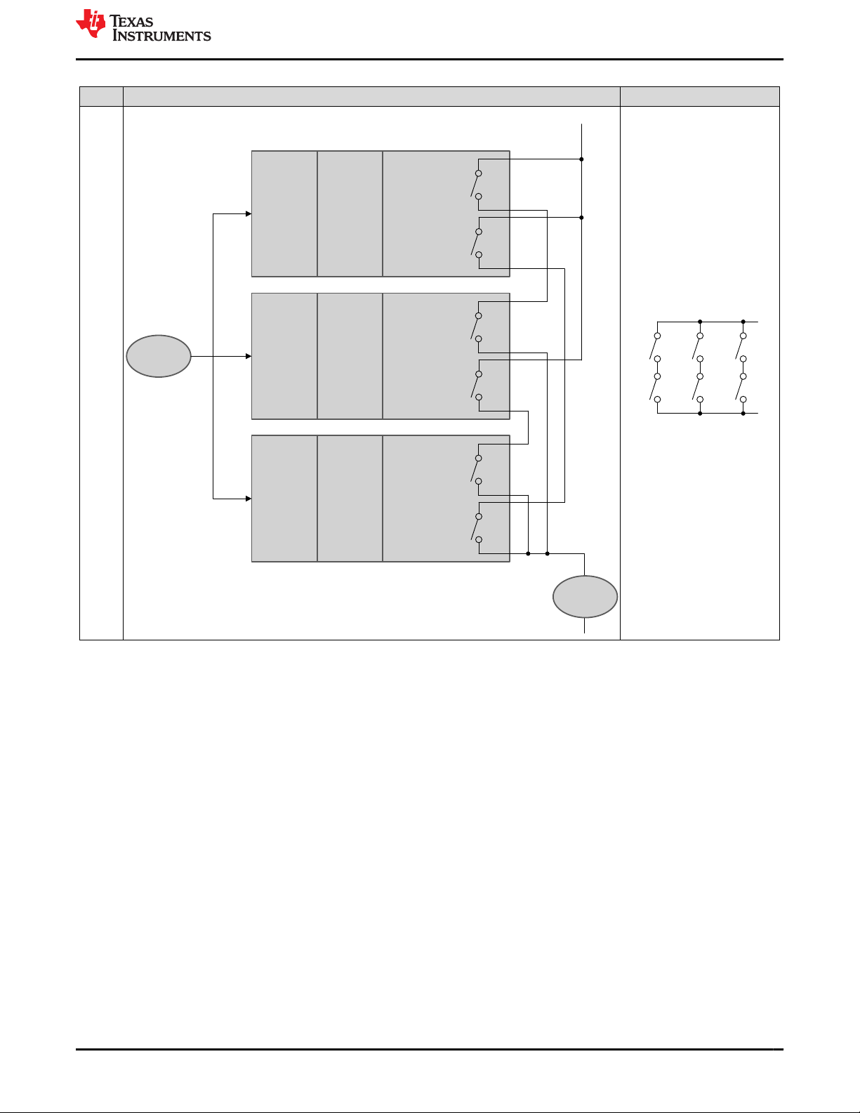
Sensor
Actuator
Final Element
-
Input
Circuit
Processing
Unit
Output Circuit 1
Output Circuit 2
Input
Circuit
Processing
Unit
Output Circuit 1
Output Circuit 2
Input
Circuit
Processing
Unit
Output Circuit 1
Output Circuit 2
A
B
A
C
B
C
Voting Circuit
www.ti.com Safety Architecture Configurations
Table A-1. Safety Architecture Configurations (continued)
Diagnostic Implementation
9 2oo3
Use three different processing
units to implement majority
voting. The fourth channel
can be used either standalone
or with hardware diagnostic
features.
SPRUIT5 – APRIL 2021
Submit Document Feedback
Copyright © 2021 Texas Instruments Incorporated
Safety Manual for TMS320F28002x 65
Page 66

Distributed Developments www.ti.com
B Distributed Developments
A Development Interface Agreement (DIA) is intended to capture the agreement between two parties towards
the management of each party’s responsibilities related to the development of a functional safety system.
Functional Safety-Compliant components are typically designed for many different systems and are considered
to be Safety Elements out of Context (SEooC) hardware components. The system integrator is then responsible
for taking the information provided in the hardware component safety manual, safety analysis report and safety
report to perform system integration activities. Because there is no distribution of development activities, TI does
not accept DIAs with system integrators.
"Functional Safety-Compliant" components are products that TI represents, promotes or markets as helping
customers mitigate functional safety related risks in an end application and/or as compliant with an industry
functional safety standard. For more information about Functional Safety-Compliant components, go to .
B.1 How the Functional Safety Lifecycle Applies to Functional Safety-Compliant Products
TI has tailored the functional safety lifecycles of ISO 26262:2018 and IEC 61508:2010 to best match the needs
of a functional Safety Element out of Context (SEooC) development. The functional safety standards are written
in the context of the functional safety systems, which means that some requirements only apply at the system
level. Since Functional Safety-Compliant components are hardware or software components, TI has tailored
the functional safety activities to create new product development processes for hardware and for software
that makes sure state-of-the-art techniques and measures are applied as appropriate. These new product
development processes have been certified by third-party functional safety experts. To find these certifications,
go to .
B.2 Activities Performed by Texas Instruments
The functional safety compliant Integrated Circuit (IC) products are hardware components developed as
functional Safety Elements out of Context. As such, TI's functional safety activities focus on those related to
management of functional safety around hardware component development. System level architecture, design,
and functional safety analysis are not within the scope of TI activities and are the responsibility of the customer.
Some techniques for integrating the SEooC safety analysis of this hardware component into the system level
can be found in ISO 26262-11:2018.
Table B-1. Activities Performed by Texas Instruments versus Performed by the customer
Functional Safety Lifecycle
Management of functional safety Yes Yes
Definition of end equipment and
assessment (of end equipment/
Creation of end equipment
Allocation of end equipment
requirements to sub-systems,
hardware components, and
Definition of hardware component
architecture and design execution
Hardware component functional
Hardware component verification
component into end equipment
Activity
item
Hazard analysis and risk
item)
functional safety concept
software components
safety requirements
Hardware component
safety analysis
and validation (V&V)
Integration of hardware
No. Assumptions made for internal development. Yes
No. Assumptions made for internal development. Yes
V&V executed to support internal development. Yes
TI Execution Customer Execution
No Yes
No Yes
Yes No
Yes No
Yes No
No Yes
66 Safety Manual for TMS320F28002x SPRUIT5 – APRIL 2021
Copyright © 2021 Texas Instruments Incorporated
Submit Document Feedback
Page 67

www.ti.com
Distributed Developments
Table B-1. Activities Performed by Texas Instruments versus Performed by the customer (continued)
Functional Safety Lifecycle
Activity
Verification of IC performance in
end equipment
Selection of safety mechanisms
to be applied to IC
End equipment level verification
and validation
End equipment level functional
safety analysis
End equipment level functional
safety assessment
End equipment release to
production
Management of functional safety
issues in production
TI Execution Customer Execution
No Yes
No Yes
No Yes
No Yes
No Yes
No Yes
Support provided as needed Yes
B.3 Information Provided
Texas instruments has summarized what it considers the most critical functional safety work products that are
available to the customer either publicly or under a nondisclosure agreement (NDA). NDAs are required to
protect proprietary and sensitive information disclosed in certain functional safety documents.
Table B-2. Product Functional Safety Documentation
Deliverable Name Contents
Functional Safety Product Preview
Functional Safety Manual
Functional Safety Analysis Report
Functional Safety Report
Assessment Certificate
(1) When an Assessment Certificate is available for a functional safety compliant product, the Functional Safety Report may not be
provided. When a Functional Safety Report is provided, an Assessment Certificate may not be available. These two documents fulfill
the same functional safety requirements and will be used interchangeably depending on the functional safety compliant product.
(1)
(1)
Overview of functional safety considerations in product development and product
architecture. Delivered ahead of public product announcement.
User guide for the functional safety features of the product, including system level
assumptions of use.
Results of all available functional safety analysis documented in a format that allows
computation of custom metrics.
Summary of arguments and evidence of compliance to functional safety standards.
References a specific component, component family, or TI process that was
analyzed.
Evidence of compliance to functional safety standards. References a specific
component, component family, or TI process that was analyzed. Provided by a 3rd
party functional safety assessor.
SPRUIT5 – APRIL 2021
Submit Document Feedback
Safety Manual for TMS320F28002x 67
Copyright © 2021 Texas Instruments Incorporated
Page 68

Summary of Safety Features and Diagnostics www.ti.com
C Summary of Safety Features and Diagnostics
C.1 Summary of Safety Features and Diagnostics
Table C-1. Summary Table Legend
Unique Identifier Identifier used to reference the contents.
Safety Feature or
Diagnostic
Usage Each test listed in this chart can be one of two types. A "diagnostic" test or a "test for diagnostic".
Diagnostic Type Hardware - A diagnostic which is implemented by TI in silicon and can communicate error status upon the
Diagnostic Operation This can be one among the following:
Test Execution Time This column lists the time required for this diagnostic to complete.
Action on Detected Fault The response this diagnostic takes when an error is detected.
Error Reporting Time Typical time required for diagnostic to indicate a detected fault to the system. For safety mechanisms where
Safety feature
Diagnostic: Provides coverage for faults on a primary function of the device. It may, in addition, provide fault
coverage on other diagnostics, and can therefore be also used as a test-for-diagnostic in certain cases
Test-for-Diagnostic Only: Does NOT provide coverage for faults on a primary function of the device. It's only
purpose is to provide fault coverage on other diagnostics
detection of failures. It may require software to enable the diagnostic and/or to take action upon the detection of
a failure.
Software - A test recommended by TI which must be created by the software implementer. This test may use
additional hardware implemented on the device by TI.
Hardware / Software - A test recommended by TI which requires both, diagnostic hardware which has been
implemented in silicon by TI, and which requires software that must be created by the software implementer.
System - A diagnostic implemented externally of the microcontroller
(i) Bootup (enabled by default)
(ii) Continuous - Enabled at reset: Hardware safety mechanism that is enabled by default at reset.
(iii) Continuous - Enabled by software: Hardware safety mechanism that needs to be enabled by software.
(iv) On demand (Software defined): Software or Hardware-software safety mechanism that gets activated in the
diagnostic test interval by the software
(v) System defined: Implemented by the system.
For software-driven tests, this action is often software implementation-dependent.
fault detection time is known, this value is indicated. For software-driven tests, this time is often software
implementation-dependent.
Table C-2. Summary of Safety Features and Diagnostic
Device
Partition
Power Supply
Clock
68 Safety Manual for TMS320F28002x SPRUIT5 – APRIL 2021
Unique
Identifier
PWR1
PWR2 External Watchdog Diagnostic
PWR4 Brownout Reset (BOR) Diagnostic Hardware
CLK1
CLK2 Clock Integrity Check
CLK3 Clock Integrity Check
CLK5 External Monitoring of
Safety Feature or
Diagnostic
External Voltage
Supervisor
Missing Clock Detect
(MCD)
Using CPU Timer
Using HRPWM
Clock via XCLKOUT
Diagnostic
Usage
Diagnostic
Diagnostic Hardware
Diagnostic Hardware -
Diagnostic Hardware -
Diagnostic System
Copyright © 2021 Texas Instruments Incorporated
Type
System
defined
System
defined
Software
Software
defined
Diagnostic
Operation
Continuous Enabled at reset
System defined
Continuous Enabled at reset
Continuous Enabled at reset
On demand
(Software
defined)
On demand
(Software
defined)
System defined System
Test
Execution
Time
Zero or very
low overhead
System
defined
Zero or very
low overhead
Zero or very
low overhead
Software
defined
Software
defined
defined
Action on
Detected
Fault
System
defined
System
defined
Reset
NMI with
ERRORSTS
assertion
Clock switch
to internal
oscillator
Software
defined
Software
defined
System
defined
Submit Document Feedback
Error
Reporting
Time
System defined
System defined
Typically less
than 1us
0.8 2ms
Software
defined
Software
defined
System defined
Page 69

www.ti.com Summary of Safety Features and Diagnostics
Table C-2. Summary of Safety Features and Diagnostic (continued)
Device
Partition
Clock (cont) CLK6 Internal Watchdog (WD) Diagnostic Hardware Continuous -
System PLL SYSPLL1 Clock integrity check
Unique
Identifier
CLK7 External Watchdog Diagnostic System
CLK8 Periodic Software Read
CLK9 Software Read Back of
CLK10 Software Test of
CLK12 Software Test of Missing
CLK13 PLL Lock Profiling using
CLK14 Peripheral Clock Gating
CLK17 Dual clock comparator
EFUSE2 Efuse ECC Diagnostic Hardware Bootup
JTAG1 Hardware disable of JTAG
SYSPLL2 PLL lock indication Diagnostic Hardware Continuous -
SYSPLL4 Internal Watchdog (WD) Diagnostic Hardware Continuous -
SYSPLL5 External Watchdog Diagnostic System System defined System
SYSPLL6 Software test of DCC
SYSPLL7 External monitoring of
SYSPLL10 Software test of
SYSPLL11 Interleaving of FSM states Fault
Safety Feature or
Diagnostic
Back of Static
Configuration Registers
Written Configuration
Watchdog (WD)
Operation
Clock Detect Functionality
On-Chip Timer
(PCLKCR)
(DCC) - Type 2
port
using DCC
functionality including
error tests
Clock
functionality including
error tests
Diagnostic
Usage
Diagnostic Software On demand
Diagnostic Software On demand
Test for
diagnostic
Test for
diagnostic
Diagnostic Hardware -
Diagnostic Hardware On demand
Diagnostic Hardware -
Fault
Avoidance
Diagnostic Hardware-
Test for
diagnostic
Diagnostic System System defined System
Diagnostic Software On demand
Avoidance
Type
defined
Software On demand
Hardware Software
Software
Software
System
defined
Software
Software On demand
Hardware Continuous -
Diagnostic
Operation
Enabled at reset
System defined System
(Software
defined)
(Software
defined)
(Software
defined)
On demand
(Software
defined)
On demand
(Software
defined)
(Software
defined)
On demand
(Software
defined)
(enabled by
default)
Continuous Enabled at reset
On demand
(Software
defined)
Enabled by
Software
Enabled by
reset
(Software
defined)
(Software
defined)
Enabled by
reset
Test
Execution
Time
Zero or very
low overhead
defined
Software
defined
Software
defined
Software
defined
Software
defined
Software
defined
NA (Fault
Avoidance)
Software
defined
Zero or very
low overhead
NA (Fault
Avoidance)
Software
defined
Software
defined
zero or very
low overhead
defined
Software
defined
defined
Software
defined
NA (Fault
Avoidance)
Action on
Detected
Fault
Device reset
or interrupt as
per
configuration
System
defined
Software
defined
Software
defined
Software
defined
Software
defined
Software
defined
NA (Fault
avoidance
technique)
Interrupt to
CPU
Device reset <400 CPU
NA (Fault
avoidance
technique)
Interrupt to
CPU
Software
defined
Device reset
of interrupt as
per
configuration
System
defined
Software
defined
System
defined
Software
defined
NA (Fault
Avoidance
technique)
Error
Reporting
Time
Software
defined
System defined
Software
defined
Software
defined
Software
defined
Software
defined
Software
defined
NA (Fault
avoidance
technique)
Typically <1 μS
to notify
*(Interrupt
handling yime is
system load
and software
dependent)
cycles
NA (Fault
avoidance
technique)
Typically <1 μS
to notify
*(Interrupt
handling yime is
system load
and software
dependent)
Software
defined
Software
defined
System defined
Software
defined
System defined
Software
defined
NA (Fault
Avoidance
technique)
SPRUIT5 – APRIL 2021
Submit Document Feedback
Safety Manual for TMS320F28002x 69
Copyright © 2021 Texas Instruments Incorporated
Page 70

Summary of Safety Features and Diagnostics www.ti.com
Table C-2. Summary of Safety Features and Diagnostic (continued)
Device
Partition
System PLL
(cont)
Reset RST1 External Monitoring of
System
Control
Module and
Configuration
Registers
EFuse EFUSE1 Efuse Autoload Self-Test Diagnostic Hardware Bootup
Unique
Identifier
CLK10 Software test of
JTAG1 Hardware disable of JTAG
RST2 Reset Cause Information Diagnostic Hardware -
RST3 Software Test of Reset Diagnostic Software On demand
RST4 Glitch Filtering on Reset
RST5 NMIWD Shadow
RST6 Periodic Software Read
RST7 Software Read Back of
RST8 NMIWD Reset
RST9 Peripheral Soft Reset
SYS1 Multi-Bit Enable Keys for
SYS2 Lock Mechanism for
SYS3 Software Read Back of
SYS4 Periodic Software Read
SYS5 Online Monitoring of
SYS8 EALLOW and MEALLOW
SYS9 Software Test of
EFUSE2 Efuse ECC Diagnostic Hardware Bootup
EFUSE4 Efuse ECC Logic Self-
Safety Feature or
Diagnostic
Watchdog (WD) operation
port
Warm Reset (XRSn)
Pins
Registers
Back of Static
Configuration Registers
Written Configuration
Functionality
(SOFTPRES)
Control Registers
Control Registers
Written Configuration
Back of Static
Configuration Registers
Temperature
Protection for Critical
Registers
ERRORSTS Functionality
Test
Diagnostic
Usage
Test for
diagnostic
Fault
Avoidance
Diagnostic System
Diagnostic Hardware Continuous -
Diagnostic Hardware -
Diagnostic Software On demand
Diagnostic Software On demand
Diagnostic Hardware Continuous -
Diagnostic Hardware On demand
Diagnostic Hardware Continuous -
Diagnostic Hardware Continuous -
Diagnostic Software On demand
Diagnostic Software On demand
Diagnostic Hardware -
Diagnostic Hardware Continuous -
Diagnostic Hardware-
Test for
diagnostic
Type
Software On demand
System
defined
defined
Software
Software
Software
Software
Hardware Bootup
Diagnostic
Operation
(Software
defined)
Continuous Enabled at reset
System defined System
On demand
(Software
defined)
(Software
defined)
Enabled at reset
On demand
(Software
defined)
(Software
defined)
(Software
defined)
Enabled at reset
(Software
defined)
Enabled at reset
Enabled by
software
(Software
defined)
(Software
defined)
On demand
(Software
defined)
Enabled at reset
On demand
(software
defined)
(enabled by
default)
(enabled by
default)
(enabled by
default)
Test
Execution
Time
Software
defined
NA (Fault
Avoidance)
defined
NA (Fault
Avoidance)
Software
defined
NA (Fault
Avoidance)
NA (Fault
Avoidance)
Software
defined
Software
defined
Zero or very
low overhead
NA (Fault
Avoidance)
NA (Fault
Avoidance)
NA (Fault
Avoidance)
Software
defined
Software
defined
Software
defined
NA (Fault
Avoidance)
Software
defined
Zero or very
low overhead
Zero or very
low overhead
Zero or very
low overhead
Action on
Detected
Fault
Software
defined
NA (Fault
avoidance
technique)
System
defined
NA (Fault
avoidance
technique)
Software
defined
NA (Fault
avoidance
technique)
NA (Fault
avoidance
technique)
Software
defined
Software
defined
Device reset Software
NA (Fault
avoidance
technique)
NA (Fault
avoidance
technique)
NA (Fault
avoidance
technique)
Software
defined
Software
defined
Software
defined
NA (Fault
avoidance
technique)
Software
defined
Device reset <400 CPU
Device reset <400 CPU
Device reset <400 CPU
Error
Reporting
Time
Software
defined
NA (Fault
avoidance
technique)
System defined
NA (Fault
avoidance
technique)
Software
defined
NA (Fault
avoidance
technique)
NA (Fault
avoidance
technique)
Software
defined
Software
defined
defined
NA (Fault
avoidance
technique)
NA (Fault
avoidance
technique)
NA (Fault
avoidance
technique)
Software
defined
Software
defined
Software
defined
NA (Fault
avoidance
technique)
Software
defined
cycles
cycles
cycles
70 Safety Manual for TMS320F28002x SPRUIT5 – APRIL 2021
Copyright © 2021 Texas Instruments Incorporated
Submit Document Feedback
Page 71

www.ti.com Summary of Safety Features and Diagnostics
Table C-2. Summary of Safety Features and Diagnostic (continued)
Device
Partition
Debug logic JTAG1 Hardware Disable of
C28x Central
Processing
Unit
Unique
Identifier
JTAG3 Internal Watchdog (WD) Diagnostic Hardware Continuous -
JTAG4 External Watchdog Diagnostic System
CPU2 CPU Hardware Built-In
CPU4 Periodic Software Read
CPU5 Access Protection
CPU7 CPU Handling of Illegal
CPU8 Internal Watchdog (WD) Diagnostic Hardware Continuous -
CPU9 External Watchdog Diagnostic System
CPU10 Information Redundancy
Safety Feature or
Diagnostic
JTAG Port
Self-Test (HWBIST)
Back of Static
Configuration Registers
Mechanism for Memories
Operation, Illegal Results
and Instruction Trapping
Techniques
Diagnostic
Usage
Diagnostic System
Diagnostic Hardware On demand
Diagnostic Software On demand
Diagnostic Hardware Continuous -
Diagnostic Hardware Continuous -
Diagnostic Software On demand
Type
defined
defined
defined
Diagnostic
Operation
Continuous Enabled at reset
Enabled at reset
System defined System
(Software
defined)
(Software
defined)
Enabled by
software
Enabled at reset
Enabled at reset
System defined System
(Software
defined)
Test
Execution
Time
NA (Fault
Avoidance)
Zero or very
low overhead
defined
Software
defined
Software
defined
Zero or very
low overhead
Zero or very
low overhead
Zero or very
low overhead
defined
Software
defined
Action on
Detected
Fault
NA (Fault
avoidance
technique)
Device reset
or interrupt as
per
configuration
System
defined
NMI with
ERRORSTS
assertion
Software
defined
Interrupt to
CPU
Interrupt to
CPU
Device reset
or interrupt as
per
configuration
System
defined
Software
defined
Error
Reporting
Time
NA (Fault
avoidance
technique)
Software
defined
System defined
Typically <1 μS
to notify
*(Interrupt
handling yime is
system load
and software
dependent)
Software
defined
Typically <1 μS
to notify
*(Interrupt
handling yime is
system load
and software
dependent)
Typically <1 μS
to notify
*(Interrupt
handling yime is
system load
and software
dependent)
Software
defined
System defined
Software
defined
SPRUIT5 – APRIL 2021
Submit Document Feedback
Safety Manual for TMS320F28002x 71
Copyright © 2021 Texas Instruments Incorporated
Page 72

Summary of Safety Features and Diagnostics www.ti.com
Table C-2. Summary of Safety Features and Diagnostic (continued)
Device
Partition
C28x Central
Processing
Unit (cont)
Unique
Identifier
CPU11 CPU Hardware Built-In
CPU12 CPU Hardware Built-In
CPU13 CPU Hardware Built-
CPU14 Stack Overflow Detection Diagnostic Hardware Continuous -
CPU15 VCRC Auto Coverage Test for
CPU18 Embedded Real Time
CPU19 Inbuilt hardware
Safety Feature or
Diagnostic
Self-Test (HWBIST) Auto
Coverage
Self-Test (HWBIST) Fault
Injection Capability
In Self-Test (HWBIST)
Timeout Feature
Analysis and Diagnostic
(ERAD)
redundancy in ERAD bus
comparator module
Diagnostic
Usage
Test for
diagnostic
Test for
diagnostic
Test for
diagnostic
diagnostic
Diagnostic Hardware -
Test for
diagnostic
Type
Hardware Continuous -
Hardware Software
Hardware Continuous -
Hardware Continuous -
Software
Hardware Software
Diagnostic
Operation
Enabled at reset
On demand
(Software
defined)
Enabled at reset
Enabled by
software
Enabled at reset
On demand
(Software
defined)
On demand
(Software
defined)
Test
Execution
Time
Zero or very
low overhead
Software
defined
Zero or very
low overhead
Zero or very
low overhead
Zero or very
low overhead
Software
defined
Software
defined
Action on
Detected
Fault
NMI with
ERRORSTS
assertion
Software
defined
NMI with
ERRORSTS
assertion
Interrupt to
CPU
Software
defined
Software
defined
Software
defined
Error
Reporting
Time
Typically <1 μS
to notify
*(Interrupt
handling yime is
system load
and software
dependent)
Software
defined
Typically <1 μS
to notify
*(Interrupt
handling yime is
system load
and software
dependent)
Typically <1 μS
to notify
*(Interrupt
handling yime is
system load
and software
dependent)
Software
defined
Software
defined
Software
defined
72 Safety Manual for TMS320F28002x SPRUIT5 – APRIL 2021
Copyright © 2021 Texas Instruments Incorporated
Submit Document Feedback
Page 73

www.ti.com Summary of Safety Features and Diagnostics
Table C-2. Summary of Safety Features and Diagnostic (continued)
Device
Partition
FPU CPU2 CPU Hardware Built-In
Flash FLASH1 Flash ECC Diagnostic Hardware Continuous -
Unique
Identifier
CPU8 Internal Watchdog (WD) Diagnostic Hardware Continuous -
CPU9 External Watchdog Diagnostic System
CPU10 Information Redundancy
CPU11 CPU Hardware Built-In
CPU12 CPU Hardware Built-In
CPU13 CPU Hardware Built-
CPU14 Stack Overflow Detection Diagnostic Hardware Continuous -
CPU18 Embedded Real Time
JTAG1 Hardware Disable of
FLASH2 VCRC Check of Static
FLASH3 Bit Multiplexing in Flash
FLASH4 Periodic Software Read
FLASH5 Software Read Back of
FLASH6 Software Test of ECC
Safety Feature or
Diagnostic
Self-Test (HWBIST)
Techniques
Self-Test (HWBIST) Auto
Coverage
Self-Test (HWBIST) Fault
Injection Capability
In Self-Test (HWBIST)
Timeout Feature
Analysis and Diagnostic
(ERAD)
JTAG Port
Memory Contents
Memory Array
Back of Static
Configuration Registers
Written Configuration
Logic
Diagnostic
Usage
Diagnostic Hardware On demand
Diagnostic Software On demand
Test for
diagnostic
Test for
diagnostic
Test for
diagnostic
Diagnostic Hardware -
Diagnostic System
Diagnostic Hardware -
Diagnostic Hardware Continuous -
Diagnostic Software On demand
Diagnostic Software On demand
Test for
diagnostic
Type
defined
Hardware Continuous -
Hardware Software
Hardware Continuous -
Software
defined
Software
Hardware Software
Diagnostic
Operation
(Software
defined)
Enabled at reset
System defined System
(Software
defined)
Enabled at reset
On demand
(Software
defined)
Enabled at reset
Enabled by
software
On demand
(Software
defined)
Continuous Enabled at reset
Enabled at reset
On demand
(Software
defined)
Enabled at reset
(Software
defined)
(Software
defined)
On demand
(Software
defined)
Test
Execution
Time
Software
defined
Zero or very
low overhead
defined
Software
defined
Zero or very
low overhead
Software
defined
Zero or very
low overhead
Zero or very
low overhead
Software
defined
NA (Fault
Avoidance)
Zero or very
low overhead
Software
defined
NA (Fault
Avoidance)
Software
defined
Software
defined
Software
defined
Action on
Detected
Fault
NMI with
ERRORSTS
assertion
Device reset
or interrupt as
per
configuration
System
defined
Software
defined
NMI with
ERRORSTS
assertion
Software
defined
NMI with
ERRORSTS
assertion
Interrupt to
CPU
Software
defined
NA (Fault
avoidance
technique)
NMI with
ERRORSTS
assertion or
interrupt to
CPU based
on error
severity
Software
defined
NA (Fault
avoidance
technique)
Software
defined
Software
defined
Software
defined
Error
Reporting
Time
Typically <1 μS
to notify
*(Interrupt
handling yime is
system load
and software
dependent)
Software
defined
System defined
Software
defined
Typically <1 μS
to notify
*(Interrupt
handling yime is
system load
and software
dependent)
Software
defined
Typically <1 μS
to notify
*(Interrupt
handling yime is
system load
and software
dependent)
Typically <1 μS
to notify
*(Interrupt
handling yime is
system load
and software
dependent)
Software
defined
NA (Fault
avoidance
technique)
Typically <1 μS
to notify
*(Interrupt
handling yime is
system load
and software
dependent)
Software
defined
NA (Fault
avoidance
technique)
Software
defined
Software
defined
Software
defined
SPRUIT5 – APRIL 2021
Submit Document Feedback
Safety Manual for TMS320F28002x 73
Copyright © 2021 Texas Instruments Incorporated
Page 74

Summary of Safety Features and Diagnostics www.ti.com
Table C-2. Summary of Safety Features and Diagnostic (continued)
Device
Partition
Flash (cont) FLASH7 Flash Program Verify and
SRAM SRAM1 SRAM ECC Diagnostic Hardware Continuous -
Unique
Identifier
FLASH8 Software Test of Flash
FLASH9 Internal Watchdog (WD) Diagnostic Hardware Continuous -
FLASH10 External Watchdog Diagnostic System
FLASH12 CPU Handling of Illegal
FLASH14 Information Redundancy
SRAM2 SRAM Parity Diagnostic Hardware Continuous -
SRAM3 Software Test of SRAM Diagnostic Software On demand
SRAM4 Bit Multiplexing in SRAM
SRAM5 Periodic Software Read
SRAM6 Software Read Back of
SRAM7 Data Scrubbing to Detect/
SRAM8 VCRC Check of Static
SRAM10 Software Test of Function
Safety Feature or
Diagnostic
Erase Verify Check
Prefetch, Data Cache and
Wait-States
Operation, Illegal Results
and Instruction Trapping
Techniques
Memory Array
Back of Static
Configuration Registers
Written Configuration
Correct Memory Errors
Memory Contents
Including Error Tests
Diagnostic
Usage
Fault
avoidance
Diagnostic Software On demand
Diagnostic Hardware Continuous -
Diagnostic Software On demand
Diagnostic Hardware Continuous -
Diagnostic Software On demand
Diagnostic Software On demand
Diagnostic Hardware -
Diagnostic Hardware -
Diagnostic Software On demand
Type
Hardware Software
defined
Software
Software
Diagnostic
Operation
On demand
(Software
defined)
(Software
defined)
Enabled at reset
System defined System
Enabled at reset
(Software
defined)
Enabled at reset
Enabled at reset
(Software
defined)
Enabled at reset
(Software
defined)
(Software
defined)
On demand
(Software
defined)
On demand
(Software
defined)
(Software
defined)
Test
Execution
Time
Software
defined
Software
defined
Zero or very
low overhead
defined
Zero or very
low overhead
Test Execution
Time: Software
defined
Zero or very
low overhead
Zero or very
low overhead
Software
defined
NA (Fault
Avoidance)
Software
defined
Software
defined
Software
defined
Software
defined
Software
defined
Action on
Detected
Fault
Software
defined
Software
defined
Device reset
or interrupt as
per
configuration
System
defined
Interrupt to
CPU
Action on
Detected
Fault:
Software
defined
NMI with
ERRORSTS
assertion or
interrupt to
CPU based
on error
severity
NMI with
ERRORSTS
assertion
Software
defined
NA (Fault
avoidance
technique)
Software
defined
Software
defined
NMI with
ERRORSTS
assertion or
interrupt to
CPU based
on error
severity
Software
defined
Software
defined
Error
Reporting
Time
Software
defined
Software
defined
Software
defined
System defined
Typically <1 μS
to notify
*(Interrupt
handling yime is
system load
and software
dependent)
Error reporting
time: Software
defined
Typically <1 μS
to notify
*(Interrupt
handling yime is
system load
and software
dependent)
Typically <1 μS
to notify
*(Interrupt
handling yime is
system load
and software
dependent)
Software
defined
NA (Fault
avoidance
technique)
Software
defined
Software
defined
Typically <1 μS
to notify
*(Interrupt
handling yime is
system load
and software
dependent)
Software
defined
Software
defined
74 Safety Manual for TMS320F28002x SPRUIT5 – APRIL 2021
Copyright © 2021 Texas Instruments Incorporated
Submit Document Feedback
Page 75

www.ti.com Summary of Safety Features and Diagnostics
Table C-2. Summary of Safety Features and Diagnostic (continued)
Device
Partition
SRAM (cont) SRAM11 Access Protection
ROM ROM1 VCRC Check of Static
Unique
Identifier
SRAM12 Lock Mechanism for
SRAM13 Software Test of ECC
SRAM14 Software Test of Parity
SRAM16 Information Redundancy
SRAM17 CPU Handling of Illegal
SRAM18 Internal Watchdog (WD) Diagnostic Hardware Continuous -
SRAM19 External Watchdog Diagnostic System
SRAM21 Memory Power-On Self-
SRAM24 Background CRC Diagnostic Hardware -
SRAM25 Watchdog for Background
ROM2 Periodic Software Read
ROM3 Software Read Back of
ROM4 Software Test of Function
ROM5 CPU Handling of Illegal
Safety Feature or
Diagnostic
Mechanism for Memories
Control Registers
Logic
Logic
Techniques
Operation, Illegal Results
and Instruction Trapping
Test (MPOST)
CRC
Memory Contents
Back of Static
Configuration Registers
Written Configuration
Including Error Tests
Operation, Illegal Results
and Instruction Trapping
Diagnostic
Usage
Diagnostic Hardware Continuous -
Diagnostic Hardware Continuous -
Test for
diagnostic
Test for
diagnostic
Diagnostic Software On demand
Diagnostic Hardware Continuous -
Diagnostic Hardware Bootup
Test for
diagnostic
Diagnostic Hardware -
Diagnostic Software On demand
Diagnostic Software On demand
Diagnostic Software On demand
Diagnostic Hardware Continuous -
Type
Hardware Software
Hardware Software
defined
Software
Hardware Software
Software
Diagnostic
Operation
Enabled by
software
Enabled by
software
On demand
(Software
defined)
On demand
(Software
defined)
(Software
defined)
Enabled at reset
Enabled at reset
System defined System
(enabled by
default)
On demand
(Software
defined)
On demand
(Software
defined)
On demand
(Software
defined)
(Software
defined)
(Software
defined)
(Software
defined)
Enabled at reset
Test
Execution
Time
Zero or very
low overhead
NA (Fault
Avoidance)
Software
defined
Software
defined
Software
defined
Zero or very
low overhead
Zero or very
low overhead
defined
Software
defined
Zreo or very
low overhead
Software
defined
Software
defined
Software
defined
Software
defined
Software
defined
Zero or very
low overhead
Action on
Detected
Fault
Interrupt to
CPU
NA (Fault
avoidance
technique)
Software
defined
Software
defined
Software
defined
Interrupt to
CPU
Device reset
or interrupt as
per
configuration
System
defined
Software
defined
NMI with
ERRORSTS
assertion or
interrupt to
CPU based
on error
severity
Software
defined
Software
defined
Software
defined
Software
defined
Software
defined
Interrupt to
CPU
Error
Reporting
Time
Typically <1 μS
to notify
*(Interrupt
handling yime is
system load
and software
dependent)
NA (Fault
avoidance
technique)
Software
defined
Software
defined
Software
defined
Typically <1 μS
to notify
*(Interrupt
handling yime is
system load
and software
dependent)
Software
defined
System defined
Software
defined
Typically < 1 uS
to notify
(Interrupt
handling time is
system load
and software
dependent)
Software
defined
Software
defined
Software
defined
Software
defined
Software
defined
Typically <1 μS
to notify
*(Interrupt
handling yime is
system load
and software
dependent)
SPRUIT5 – APRIL 2021
Submit Document Feedback
Safety Manual for TMS320F28002x 75
Copyright © 2021 Texas Instruments Incorporated
Page 76

Summary of Safety Features and Diagnostics www.ti.com
Table C-2. Summary of Safety Features and Diagnostic (continued)
Device
Partition
ROM (cont) ROM6 Internal Watchdog (WD) Diagnostic Hardware Continuous -
Device
Interconnect
Direct Memory
Access (DMA)
Unique
Identifier
ROM7 External Watchdog Diagnostic System
ROM8 Power-Up Pre-
ROM10 Memory Power-On Self-
INC1 Software Test of Function
INC2 Internal Watchdog (WD) Diagnostic Hardware Continuous -
INC3 External Watchdog Diagnostic System
INC4 Periodic Software Read
INC5 Software Read Back of
INC6 CPU Handling of Illegal
INC8 Transmission
INC9 Hardware Redundancy Diagnostic Hardware -
INC11 Timeout detection through
ERAD1 Software test of
DMA2 Information Redundancy
DMA3 Transmission
DMA4 Periodic Software Read
DMA5 Software Read Back of
DMA6 Software Test of Function
Safety Feature or
Diagnostic
Operational Security
Checks
Test (MPOST)
Including Error Tests
Back of Static
Configuration Registers
Written Configuration
Operation, Illegal Results
and Instruction Trapping
Redundancy
ERAD counter
functionality including
error tests
Techniques
Redundancy
Back of Static
Configuration Registers
Written Configuration
Including Error Tests
Diagnostic
Usage
Diagnostic Software On demand
Diagnostic Hardware Bootup
Diagnostic Software On demand
Diagnostic Software On demand
Diagnostic Software On demand
Diagnostic Hardware Continuous -
Diagnostic Software On demand
Diagnostic Hardware Continuous -
Test for
diagnostic
Diagnostic Software On demand
Diagnostic Software On demand
Diagnostic Software On demand
Diagnostic Software On demand
Diagnostic Software On demand
Type
defined
defined
Software
Software On demand
Diagnostic
Operation
Enabled at reset
System defined System
(Software
defined)
(enabled by
default)
(Software
defined)
Enabled at reset
System defined System
(Software
defined)
(Software
defined)
Enabled at reset
(Software
defined)
On demand
(Software
defined)
Enabled by
software
(Software
defined)
(Software
defined)
(Software
defined)
(Software
defined)
(Software
defined)
(Software
defined)
Test
Execution
Time
Zero or very
low overhead
defined
Software
defined
Software
defined
Software
defined
Zero or very
low overhead
defined
Software
defined
Software
defined
Zero or very
low overhead
Software
defined
Software
defined
Zero or very
low overhead
Software
defined
Software
defined
Software
defined
Software
defined
Software
defined
Software
defined
Action on
Detected
Fault
Device reset
or interrupt as
per
configuration
System
defined
Software
defined
Software
defined
Software
defined
Device reset
or interrupt as
per
configuration
System
defined
Software
defined
Software
defined
Interrupt to
CPU
Software
defined
Software
defined
Interrupt to
CPU
Software
defined
Software
Defined
System
Defined
Software
defined
Software
defined
Software
Defined
Error
Reporting
Time
Software
defined
System defined
Software
defined
Software
defined
Software
defined
Software
defined
System defined
Software
defined
Software
defined
Typically <1 μS
to notify
*(Interrupt
handling yime is
system load
and software
dependent)
Software
defined
Software
defined
Typically <1 μS
to notify
*(Interrupt
handling yime is
system load
and software
dependent)
Software
defined
Software
defined
Software
defined
Software
defined
Software
defined
Software
defined
76 Safety Manual for TMS320F28002x SPRUIT5 – APRIL 2021
Copyright © 2021 Texas Instruments Incorporated
Submit Document Feedback
Page 77

www.ti.com Summary of Safety Features and Diagnostics
Table C-2. Summary of Safety Features and Diagnostic (continued)
Device
Partition
DMA (cont) DMA7 DMA Overflow Interrupt Diagnostic Hardware Continuous -
Enhanced
Peripheral
Interrupt
Expander
(ePIE)
Dual Zone
Code Security
Module
(DCSM)
Unique
Identifier
DMA8 Access Protection
DMA9 Disabling of Unused DMA
PIE1 PIE Double SRAM
PIE2 Software Test of SRAM Diagnostic Software On demand
PIE3 Software Test of ePIE
PIE4 Periodic Software Read
PIE5 Software Read Back of
PIE6 PIE Double SRAM
PIE7 Maintaining Interrupt
PIE8 Online Monitoring of
DCSM1 Multi-Bit Enable Keys for
DCSM2 Majority Voting and Error
DCSM3 Periodic Software Read
DCSM4 Software Test of Function
DCSM5 Software Read Back of
Safety Feature or
Diagnostic
Mechanism for Memories
Trigger Sources
Hardware Comparison
Operation Including Error
Tests
Back of Static
Configuration Registers
Written Configuration
Comparison Check
Handler for Unused
Interrupts
Interrupts and Events
Control Registers
Detection of Link Pointer
Back of Static
Configuration Registers
Including Error Tests
Written Configuration
Diagnostic
Usage
Diagnostic Hardware Continuous -
Fault
avoidance
Diagnostic Hardware Continuous -
Diagnostic Hardware -
Diagnostic Software On demand
Diagnostic Software On demand
Test for
diagnostic
Diagnostic Hardware Continuous -
Diagnostic Software On demand
Diagnostic Hardware Continuous -
Diagnostic Hardware Continuous -
Diagnostic Software On demand
Diagnostic Software On demand
Diagnostic Software On demand
Type
Software On demand
Software
Software On demand
Diagnostic
Operation
Enabled at reset
Enabled by
software
(Software
defined)
Enabled at reset
(Software
defined)
On demand
(Software
defined)
(Software
defined)
(Software
defined)
(Software
defined)
Enabled by
software
(Software
defined)
Enabled at reset
Enabled at reset
(Software
defined)
(Software
defined)
(Software
defined)
Test
Execution
Time
Zero or very
low overhead
Zero or very
low overhead
Software
defined
Zero or very
low overhead
Software
defined
Software
defined
Software
defined
Software
defined
Software
defined
Zero or very
low overhead
Software
defined
NA (Fault
Avoidance)
NA (Fault
Avoidance)
Software
defined
Software
defined
Software
defined
Action on
Detected
Fault
Interrupt to
CPU
Interrupt to
CPU
Software
defined
CPU
exception for
single core
device, NMI
with
ERRORSTS
assertion for
dual core
device
Software
defined
Software
defined
Software
defined
Software
defined
Software
defined
Software
defined
Software
defined
NA (Fault
avoidance
technique)
NA (Fault
avoidance
technique)
Software
defined
Software
defined
Software
defined
Error
Reporting
Time
Typically <1 μS
to notify
*(Interrupt
handling yime is
system load
and software
dependent)
Typically <1 μS
to notify
*(Interrupt
handling yime is
system load
and software
dependent)
Software
defined
Typically <1 μS
to notify
*(Interrupt
handling yime is
system load
and software
dependent)
Software
defined
Software
defined
Software
defined
Software
defined
Software
defined
Software
defined
Software
defined
NA (Fault
avoidance
technique)
NA (Fault
avoidance
technique)
Software
defined
Software
defined
Software
defined
SPRUIT5 – APRIL 2021
Submit Document Feedback
Safety Manual for TMS320F28002x 77
Copyright © 2021 Texas Instruments Incorporated
Page 78

Summary of Safety Features and Diagnostics www.ti.com
Table C-2. Summary of Safety Features and Diagnostic (continued)
Device
Partition
DCSM (cont) DCSM6 CPU Handling of Illegal
Cross Bar (XBAR)
Timer TIM1 1oo2 Software Voting
Configurable
Logic Block
(CLB)
Unique
Identifier
DCSM8 VCRC Check of Static
DCSM9 External Watchdog Diagnostic System
DCSM11 Hardware Redundancy Diagnostic Software On demand
XBAR1 Software Test of Function
XBAR2 Hardware Redundancy Diagnostic Hardware Continuous -
XBAR3 Periodic Software Read
XBAR4 Software Read Back of
XBAR5 Software Check of X-BAR
TIM2 Periodic Software Read
TIM3 Software Read Back of
TIM4 Software Test of Function
CLB1 Software test of CLB
CLB2 Hardware Redundancy Diagnostic Hardware -
CLB3 Monitoring of CLB by
CLB4 Periodic Software Read
CLB5 Software Read Back of
CLB6 Lock Mechanism for
CLB7 Internal Watchdog (WD) Diagnostic Hardware Continuous -
Safety Feature or
Diagnostic
Operation, Illegal Results
and Instruction Trapping
Memory Contents
Including Error Tests
Back of Static
Configuration Registers
Written Configuration
Flag
Using Secondary Free
Running Counter
Back of Static
Configuration Registers
Written Configuration
Including Error Tests
Function including Error
Tests
eCAP or eQEP
Back of Static
Configuration Registers
Written Configuration
Control Registers
Diagnostic
Usage
Diagnostic Hardware Continuous -
Diagnostic Hardware -
Diagnostic Software On demand
Diagnostic Software On demand
Diagnostic Software On demand
Diagnostic Software On demand
Diagnostic Hardware -
Diagnostic Software On demand
Diagnostic Software On demand
Diagnostic Software On demand
Diagnostic Software On demand
Diagnostic Hardware -
Diagnostic Software On demand
Diagnostic Software On demand
Diagnostic Hardware Continuous -
Type
Software
defined
Software
Software
Software
Diagnostic
Operation
Enabled at reset
On demand
(Software
defined)
System defined System
(Software
defined)
(Software
defined)
Enabled by
software
(Software
defined)
(Software
defined)
(Software
defined)
On demand
(Software
defined)
(Software
defined)
(Software
defined)
(Software
defined)
(Software
defined)
On demand
(Software
defined)
On demand
(Software
defined)
(Software
defined)
(Software
defined)
Enabled by
software
Enabled at reset
Test
Execution
Time
Zero or very
low overhead
Software
defined
defined
Software
defined
Software
defined
Zero or very
low overhead
Software
defined
Software
defined
Software
defined
Software
defined
Software
defined
Software
defined
Software
defined
Software
defined
Software
defined
Software
defined
Software
defined
Software
defined
NA (Fault
Avoidance)
Zero or very
low overhead
Action on
Detected
Fault
Interrupt to
CPU
Software
defined
System
defined
Software
defined
Software
defined
Software
defined
Software
defined
Software
defined
Software
defined
Software
defined
Software
defined
Software
defined
Software
defined
Software
defined
Software
defined
Software
defined
Software
defined
Software
defined
NA (Fault
avoidance
technique)
Device reset
or interrupt as
per
configuration
Error
Reporting
Time
Typically <1 μS
to notify
*(Interrupt
handling yime is
system load
and software
dependent)
Software
defined
System defined
Software
defined
Software
defined
Software
defined
Software
defined
Software
defined
Software
defined
Software
defined
Software
defined
Software
defined
Software
defined
Software
defined
Software
defined
Software
defined
Software
defined
Software
defined
NA (Fault
avoidance
technique)
Software
defined
78 Safety Manual for TMS320F28002x SPRUIT5 – APRIL 2021
Copyright © 2021 Texas Instruments Incorporated
Submit Document Feedback
Page 79

www.ti.com Summary of Safety Features and Diagnostics
Table C-2. Summary of Safety Features and Diagnostic (continued)
Device
Partition
CLB (cont) CLB8 Periodic Software Read
General
Pupose I/O
and
Multiplexing
(GPIO and
PINMUX)
Enhanced
Pulse Width
Modulators
(ePWM)
High
Resolution
Capture
(HRCAP)
Unique
Identifier
JTAG1 Hardware Disable of
GPIO1 Lock Mechanism for
GPIO2 Periodic Software Read
GPIO3 Software Read Back of
GPIO4 Software Test of Function
GPIO5 Hardware Redundancy Diagnostic Hardware -
PWM1 Software Test of Function
PWM2 Hardware Redundancy Diagnostic Hardware Continuous -
PWM3 Monitoring of ePWM by
PWM4 Periodic Software Read
PWM5 Software Read Back of
PWM6 Lock Mechanism for
PWM8 ePWM Fault Detection
PWM9 ePWM Synchronization
PWM11 ePWM Application Level
PWM12 Online Monitoring of
PWM13 Monitoring of ePWM by
HRCAP1 Software Test of Function
HRCAP2 Hardware Redundancy Diagnostic Hardware -
Safety Feature or
Diagnostic
Back of SPI buffer
JTAG Port
Control Registers
Back of Static
Configuration Registers
Written Configuration
Using I/O Loopback
Including Error Tests
eCAP
Back of Static
Configuration Registers
Written Configuration
Control Registers
using XBAR
Check
Safety Mechanism
Periodic Interrupts and
Events
ADC
Including Error Tests
Diagnostic
Usage
Diagnostic Software On demand
Diagnostic System
Diagnostic Hardware Continuous -
Diagnostic Software On demand
Diagnostic Software On demand
Diagnostic Software On demand
Diagnostic Software On demand
Diagnostic Hardware -
Diagnostic Software On demand
Diagnostic Software On demand
Fault
avoidance
Diagnostic Hardware Continuous -
Diagnostic Software On demand
Diagnostic Software On demand
Diagnostic Software On demand
Diagnostic System
Diagnostic Software On demand
Type
defined
Software
Software
Hardware Continuous -
defined
Software
Diagnostic
Operation
(Software
defined)
Continuous Enabled at reset
Enabled by
software
(Software
defined)
(Software
defined)
(Software
defined)
On demand
(Software
defined)
(Software
defined)
Enabled by
software
On demand
(Software
defined)
(Software
defined)
(Software
defined)
Enabled by
software
Enabled by
software
(Software
defined)
(Software
defined)
(Software
defined)
On demand
(Software
defined)
(Software
defined)
On demand
(Software
defined)
Test
Execution
Time
Software
defined
NA (Fault
Avoidance)
NA (Fault
Avoidance)
Software
defined
Software
defined
Software
defined
Software
defined
Software
defined
Zero or very
low overhead
Software
defined
Software
defined
Software
defined
NA (Fault
Avoidance)
Zero or very
low overhead
Software
defined
Software
defined
Software
defined
On demand
(Software
defined)
Software
defined
Software
defined
Action on
Detected
Fault
Software
defined
NA (Fault
avoidance
technique)
NA (Fault
avoidance
technique)
Software
defined
Software
defined
Software
defined
Software
defined
Software
defined
Software
defined
Software
defined
Software
defined
Software
defined
NA (Fault
avoidance
technique)
Software
defined
Software
defined
Software
defined
Software
defined
Software
defined
Software
defined
Software
defined
Error
Reporting
Time
Software
defined
NA (Fault
avoidance
technique)
NA (Fault
avoidance
technique)
Software
defined
Software
defined
Software
defined
Software
defined
Software
defined
Software
defined
Software
defined
Software
defined
Software
defined
NA (Fault
avoidance
technique)
Software
defined
Software
defined
Software
defined
Software
defined
Software
defined
Software
defined
Software
defined
SPRUIT5 – APRIL 2021
Submit Document Feedback
Safety Manual for TMS320F28002x 79
Copyright © 2021 Texas Instruments Incorporated
Page 80

Summary of Safety Features and Diagnostics www.ti.com
Table C-2. Summary of Safety Features and Diagnostic (continued)
Device
Partition
HRCAP (cont) HRCAP3 Monitoring of HRPWM by
High
Resolution
Pulse Width
Modulator
(HRPWM)
Enhanced
Capture
(eCAP)
Enhanced
Quadrature
Encoder Pulse
(eQEP)
Unique
Identifier
HRCAP4 Periodic Software Read
HRCAP5 Software Read Back of
HRCAP7 HRCAP Calibration Logic
OTTO1 HRPWM Built-In Self-
OTTO2 Hardware Redundancy Diagnostic Hardware On demand
OTTO3 Monitoring of ePWM by
OTTO4 Periodic Software Read
OTTO5 Software Read Back of
CAP1 Software Test of Function
CAP2 Information Redundancy
CAP3 Monitoring of ePWM by
CAP4 Periodic Software Read
CAP5 Software Read Back of
CAP6 eCAP Application Level
CAP7 Hardware Redundancy Diagnostic Hardware -
QEP1 Software Test of Function
QEP2 eQEP Quadrature
QEP3 Information Redundancy
Safety Feature or
Diagnostic
HRCAP
Back of Static
Configuration Registers
Written Configuration
Test Feature
Check and Diagnostic
Capabilities
eCAP
Back of Static
Configuration Registers
Written Configuration
Including Error Tests
Techniques
eCAP
Back of Static
Configuration Registers
Written Configuration
Safety Mechanism
Including Error Tests
Watchdog
Techniques
Diagnostic
Usage
Test for
diagnostic
Diagnostic Software On demand
Diagnostic Software On demand
Diagnostic Hardware -
Diagnostic Software On demand
Diagnostic Hardware -
Diagnostic Software On demand
Diagnostic Software On demand
Diagnostic Software On demand
Diagnostic Hardware -
Test for
diagnostic
Diagnostic Software On demand
Diagnostic Software On demand
Diagnostic Software On demand
Diagnostic Software On demand
Diagnostic Hardware Continuous -
Diagnostic Hardware -
Type
Hardware Software
Software
Software
Software
Hardware Software
Software
Software
Diagnostic
Operation
On demand
(Software
defined)
(Software
defined)
(Software
defined)
On demand
(Software
defined)
(Software
defined)
(Software
defined)
On demand
(Software
defined)
(Software
defined)
(Software
defined)
(Software
defined)
On demand
(Software
defined)
On demand
(Software
defined)
(Software
defined)
(Software
defined)
(Software
defined)
On demand
(Software
defined)
(Software
defined)
Enabled by
software
On demand
(Software
defined)
Test
Execution
Time
Software
defined
Software
defined
Software
defined
Software
defined
Software
defined
Software
defined
Software
defined
Software
defined
Software
defined
Software
defined
Software
defined
Software
defined
Software
defined
Software
defined
Software
defined
Software
defined
Software
defined
Zero or very
low overhead
Software
defined
Action on
Detected
Fault
Software
defined
Software
defined
Software
defined
Software
defined
Software
defined
Software
defined
Software
defined
Software
defined
Software
defined
Software
defined
Software
defined
Software
defined
Software
defined
Software
defined
Software
defined
Software
defined
Software
defined
Interrupt to
CPU
Software
defined
Error
Reporting
Time
Software
defined
Software
defined
Software
defined
Software
defined
Software
defined
Software
defined
Software
defined
Software
defined
Software
defined
Software
defined
Software
defined
Software
defined
Software
defined
Software
defined
Software
defined
Software
defined
Software
defined
Typically <1 μS
to notify
*(Interrupt
handling yime is
system load
and software
dependent)
Software
defined
80 Safety Manual for TMS320F28002x SPRUIT5 – APRIL 2021
Copyright © 2021 Texas Instruments Incorporated
Submit Document Feedback
Page 81

www.ti.com Summary of Safety Features and Diagnostics
Table C-2. Summary of Safety Features and Diagnostic (continued)
Device
Partition
eQEP (cont) QEP4 Periodic Software Read
Local
Interconnect
Network (LIN)
Unique
Identifier
QEP5 Software Read Back of
QEP6 eQEP Application Level
QEP7 Hardware Redundancy Diagnostic Hardware -
QEP8 QMA Error Detection
QEP9 eQEP Software Test
LIN1 Software Test of Function
LIN2 Information Redundancy
LIN3 Transmission
LIN4 Periodic Software Read
LIN5 Software Read Back of
LIN6 Data Parity Error
LIN7 Overrun Error Detection Diagnostic Hardware Continuous -
LIN8 Frame Error Detection Diagnostic Hardware Continuous -
LIN9 LIN Physical Bus Error
LIN10 LIN No-Response Error
Safety Feature or
Diagnostic
Back of Static
Configuration Registers
Written Configuration
Safety Mechanism
Logic
of Quadrature Watchdog
Functionality
Using I/O Loopback
Techniques Including
End-to-End Safing
Redundancy
Back of Static
Configuration Registers
Written Configuration
Detection
Detection
Detection
Diagnostic
Usage
Diagnostic Software On demand
Diagnostic Software On demand
Diagnostic Software On demand
Diagnostic Hardware Continuous -
Test for
diagnostic
Diagnostic Hardware -
Diagnostic Software On demand
Diagnostic Software On demand
Diagnostic Software On demand
Diagnostic Software On demand
Diagnostic Software On demand
Diagnostic Hardware Continuous -
Diagnostic Hardware Continuous -
Type
Software
Software On demand
Software
Diagnostic
Operation
(Software
defined)
(Software
defined)
(Software
defined)
On demand
(Software
defined)
Enabled at reset
(Software
defined)
On demand
(Software
defined)
(Software
defined)
(Software
defined)
(Software
defined)
(Software
defined)
(Software
defined)
Enabled by
software
Enabled by
software
Enabled by
software
Enabled by
software
Test
Execution
Time
Software
defined
Software
defined
Software
defined
Software
defined
Zero or very
low overhead
Software
defined
Software
defined
Software
defined
Software
defined
Software
defined
Software
defined
Software
defined
Zero or very
low overhead
Zero or very
low overhead
Zero or very
low overhead
Zero or very
low overhead
Action on
Detected
Fault
Software
defined
Software
defined
Software
defined
Software
defined
Interrupt to
CPU
Software
defined
Software
defined
Software
defined
Software
defined
Software
defined
Software
defined
Software
defined
Interrupt to
CPU
Interrupt to
CPU
Interrupt to
CPU
Interrupt to
CPU
Error
Reporting
Time
Software
defined
Software
defined
Software
defined
Software
defined
Typically <1 μS
to notify
*(Interrupt
handling yime is
system load
and software
dependent)
Software
defined
Software
defined
Software
defined
Software
defined
Software
defined
Software
defined
Software
defined
Typically less
than 1 µs to
notify *(Interrupt
Handling Time
is System Load
and Software
Dependent)
Typically less
than 1 µs to
notify *(Interrupt
Handling Time
is System Load
and Software
Dependent)
Typically less
than 1 µs to
notify *(Interrupt
Handling Time
is System Load
and Software
Dependent)
Typically less
than 1 µs to
notify *(Interrupt
Handling Time
is System Load
and Software
Dependent)
SPRUIT5 – APRIL 2021
Submit Document Feedback
Safety Manual for TMS320F28002x 81
Copyright © 2021 Texas Instruments Incorporated
Page 82

Summary of Safety Features and Diagnostics www.ti.com
Table C-2. Summary of Safety Features and Diagnostic (continued)
Device
Partition
LIN (cont) LIN11 Bit Error Detection Diagnostic Hardware Continuous -
Fast Serial
Interface (FSI)
Unique
Identifier
LIN12 LIN Checksum Error
LIN13 LIN ID Parity Error
LIN15 SCI Break Error Detection Diagnostic Hardware Continuous -
LIN16 Communication Access
FSI1 Software Test of Function
FSI2 Information Redundancy
FSI3 Periodic Software Read
FSI4 Software Read Back of
FSI5 Transmission
FSI6 FSI Data Overrun/
FSI7 FSI Frame Overrun
FSI8 FSI CRC Framing Checks Diagnostic Hardware Continuous -
Safety Feature or
Diagnostic
Detection
Detection
Latency Profiling Using
On-Chip Timer
Using I/O Loopback
Techniques Including
End-to-End Safing
Back of Static
Configuration Registers
Written Configuration
Redundancy
Underrun Detection
Detection
Diagnostic
Usage
Diagnostic Hardware Continuous -
Diagnostic Hardware Continuous -
Diagnostic Hardware -
Diagnostic Hardware -
Diagnostic Hardware -
Diagnostic Software On demand
Diagnostic Software On demand
Diagnostic Software On demand
Diagnostic Hardware Continuous -
Diagnostic Hardware Continuous -
Type
Software
Software
Software
Diagnostic
Operation
Enabled by
software
Enabled by
software
Enabled by
software
Enabled by
software
On demand
(Software
defined)
On demand
(Software
defined)
On demand
(Software
defined)
(Software
defined)
(Software
defined)
(Software
defined)
Enabled by
software
Enabled by
software
Enabled by
software
Test
Execution
Time
Zero or very
low overhead
Zero or very
low overhead
Zero or very
low overhead
Zero or very
low overhead
Software
defined
Software
defined
Software
defined
Software
defined
Software
defined
Software
defined
Zero or very
low overhead
Zero or very
low overhead
Zero or very
low overhead
Action on
Detected
Fault
Interrupt to
CPU
Interrupt to
CPU
Interrupt to
CPU
Interrupt to
CPU
Software
defined
Software
defined
Software
defined
Software
defined
Software
defined
Software
defined
Interrupt to
CPU
Interrupt to
CPU
Interrupt to
CPU
Error
Reporting
Time
Typically less
than 1 µs to
notify *(Interrupt
Handling Time
is System Load
and Software
Dependent)
Typically less
than 1 µs to
notify *(Interrupt
Handling Time
is System Load
and Software
Dependent)
Typically less
than 1 µs to
notify *(Interrupt
Handling Time
is System Load
and Software
Dependent)
Typically <1 μS
to notify
*(Interrupt
handling yime is
system load
and software
dependent)
Software
defined
Software
defined
Software
defined
Software
defined
Software
defined
Software
defined
Typically less
than 1 µs to
notify *(Interrupt
Handling Time
is System Load
and Software
Dependent)
Typically less
than 1 µs to
notify *(Interrupt
Handling Time
is System Load
and Software
Dependent)
Typically <1 μS
to notify
*(Interrupt
handling yime is
system load
and software
dependent)
82 Safety Manual for TMS320F28002x SPRUIT5 – APRIL 2021
Copyright © 2021 Texas Instruments Incorporated
Submit Document Feedback
Page 83

www.ti.com Summary of Safety Features and Diagnostics
Table C-2. Summary of Safety Features and Diagnostic (continued)
Device
Partition
FSI (cont) FSI9 FSI ECC Framing Checks Diagnostic Hardware -
Power
Management
Bus Module
(PMBus)
Unique
Identifier
FSI10 FSI Frame Watchdog Diagnostic Hardware Continuous -
FSI11 FSI RX Ping Watchdog Diagnostic Hardware Continuous -
FSI12 FSI Tag Monitor Diagnostic Software On demand
FSI13 FSI Frame Type Error
FSI14 FSI End of Frame Error
FSI15 FSI Register Protection
PMBUS2 I2C Data Acknowledge
PMBUS3 Information Redundancy
PMBUS4 Periodic Software Read
PMBUS5 Software Read Back of
PMBUS6 Transmission
PMBUS7 PMBus Protocol CRC in
PMBUS8 Clock Timeout Diagnostic Hardware Continuous -
Safety Feature or
Diagnostic
Detection
Detection
Mechanisms
Check
Techniques Including
End-to-End Safing
Back of Static
Configuration Registers
Written Configuration
Redundancy
Message
Diagnostic
Usage
Diagnostic Hardware Continuous -
Diagnostic Hardware Continuous -
Fault
avoidance
Diagnostic Hardware -
Diagnostic Software On demand
Diagnostic Software On demand
Diagnostic Software On demand
Diagnostic Software On demand
Diagnostic Hardware -
Type
Software
Hardware Continuous -
Software
Software
Diagnostic
Operation
On demand
(Software
defined)
Enabled by
software
Enabled by
software
(Software
defined)
Enabled by
software
Enabled by
software
Enabled by
software
On demand
(Software
defined)
(Software
defined)
(Software
defined)
(Software
defined)
(Software
defined)
On demand
(Software
defined)
Enabled by
software
Test
Execution
Time
Software
defined
Zero or very
low overhead
Zero or very
low overhead
Software
defined
Zero or very
low overhead
Zero or very
low overhead
NA (Fault
Avoidance)
Software
defined
Software
defined
Software
defined
Software
defined
Software
defined
Software
defined
Zero or very
low overhead
Action on
Detected
Fault
Software
defined
Interrupt to
CPU
Interrupt to
CPU
Software
defined
Interrupt to
CPU
Interrupt to
CPU
NA (Fault
Avoidance)
Software
defined
Software
defined
Software
defined
Software
defined
Software
defined
Software
defined
Interrupt to
CPU
Error
Reporting
Time
Software
defined
Typically less
than 1 µs to
notify *(Interrupt
Handling Time
is System Load
and Software
Dependent)
Typically <1 μS
to notify
*(Interrupt
handling yime is
system load
and software
dependent)
Software
defined
Typically less
than 1 µs to
notify *(Interrupt
Handling Time
is System Load
and Software
Dependent)
Typically <1 μS
to notify
*(Interrupt
handling yime is
system load
and software
dependent)
NA (Fault
Avoidance)
Software
defined
Software
defined
Software
defined
Software
defined
Software
defined
Software
defined
Typically <1 μS
to notify
*(Interrupt
handling yime is
system load
and software
dependent)
SPRUIT5 – APRIL 2021
Submit Document Feedback
Safety Manual for TMS320F28002x 83
Copyright © 2021 Texas Instruments Incorporated
Page 84

Summary of Safety Features and Diagnostics www.ti.com
Table C-2. Summary of Safety Features and Diagnostic (continued)
Device
Partition
HIC HIC1 Periodic Software Read
XINT XINT1 Software Test of Function
Analog-toDigital
Converter
(ADC)
Unique
Identifier
HIC2 Signature mechanism
HIC3 Software timeout
HIC4 Access protection enable
HIC5 Software Read Back of
HIC6 Detection of illegal access
HIC7 Detection of simultaneous
HIC8 Enabling the locking
HIC9 Software test of function
HIC10 Transmission
HIC11 Information Redundancy
HIC12 Disabling of unused
CLK6 Internal Watchdog (WD) Diagnostic Hardware Continuous -
JTAG1 Hardware Disable of
XINT2 Periodic Software Read
XINT3 Software Read Back of
XINT4 Hardware Redundancy Diagnostic Hardware Continuous -
ADC1 Software Test of Function
Safety Feature or
Diagnostic
Back of Static
Configuration Registers
for interrupt and
acknowledgement in
software
mechanism for interrupt
logic
for read/write operations
in software
Written Configuration
sequences or access
types from host to device
MMR access by host and
device
mechanism for registers
including error tests
Redundancy
Techniques Including
End-to-End Safing
EVENTRIG trigger
sources
JTAG Port
Including Error Tests
Back of Static
Configuration Registers
Written Configuration
Including Error Tests
Diagnostic
Usage
Diagnostic Software On demand
Diagnostic Software Continuous Software
Diagnostic Software On demand
Diagnostic Software Continuous Software
Diagnostic Software On demand
Diagnostic Hardware Continuous -
Diagnostic Hardware Continuous -
Fault
Avoidance
Diagnostic Software Continuous Software
Diagnostic Software Continuous Software
Diagnostic Software Continuous Software
Fault
Avoidance
Fault
Avoidance
Diagnostic Software On demand
Diagnostic Software On demand
Diagnostic Software On demand
Diagnostic Software On demand
Type
Hardware Continuous -
Hardware Continuous -
System
defined
Diagnostic
Operation
(Software
defined)
(Software
defined)
(Software
defined)
Enabled by
software
Enabled by
software
Enabled by
software
Enabled by
software
Enabled at reset
Continuous Enabled at reset
(Software
defined)
(Software
defined)
(Software
defined)
Enabled by
software
(Software
defined)
Test
Execution
Time
Software
defined
defined
Software
defined
defined
Software
defined
Zero or very
low overhead
Zero or very
low overhead
Zero or very
low overhead
defined
defined
defined
Zero or very
low overhead
Zero or very
low overhead
NA (Fault
Avoidance)
Software
defined
Software
defined
Software
defined
Zero or very
low overhead
Software
defined
Action on
Detected
Fault
Software
defined
Software
defined
Software
defined
Software
defined
Software
defined
Interrupt to
CPU
Interrupt to
CPU
NA (Fault
avoidance
technique)
Software
defined
Software
defined
Software
defined
NA (Fault
avoidance
technique)
Device reset
or interrupt as
per
configuration
NA (Fault
avoidance
technique)
Software
defined
Software
defined
Software
defined
Software
defined
Software
defined
Error
Reporting
Time
Software
dependent
Software
dependent
Software
dependent
Software
dependent
Software
dependent
Typically <1 μS
to notify
*(Interrupt
handling yime is
system load
and software
dependent)
Typically <1 μS
to notify
*(Interrupt
handling yime is
system load
and software
dependent)
NA (Fault
avoidance
technique)
Software
dependent
Software
dependent
Software
dependent
NA (Fault
avoidance
technique)
Software
defined
NA (Fault
avoidance
technique)
Software
defined
Software
defined
Software
defined
Software
defined
Software
defined
84 Safety Manual for TMS320F28002x SPRUIT5 – APRIL 2021
Copyright © 2021 Texas Instruments Incorporated
Submit Document Feedback
Page 85

www.ti.com Summary of Safety Features and Diagnostics
Table C-2. Summary of Safety Features and Diagnostic (continued)
Device
Partition
ADC (cont) ADC2 DAC to ADC Loopback
CMPSS CMPSS1 Software Test of Function
Controller
Area Network
(DCAN)
Unique
Identifier
ADC3 ADC Information
ADC4 Opens/Shorts Detection
ADC5 Software Read Back of
ADC6 Periodic Software Read
ADC7 ADC Signal Quality
ADC8 ADC Input Signal Integrity
ADC9 Monitoring of ePWM by
ADC10 Hardware Redundancy Diagnostic Hardware -
ADC11 Disabling Unused
CMPSS3 Hardware Redundancy Diagnostic Hardware Continuous -
CMPSS4 Software Read Back of
CMPSS5 Periodic Software Read
CMPSS6 Lock Mechanism for
CMPSS7 VDAC Conversion by
CMPSS8 CMPSS Ramp Generator
CAN1 Software Test of Function
CAN2 Information Redundancy
CAN3 SRAM Parity Diagnostic Hardware Continuous -
Safety Feature or
Diagnostic
Check
Redundancy Techniques
Circuit for ADC
Written Configuration
Back of Static
Configuration Registers
Check by Varying
Acquisition Window
Check
ADC
Sources of SOC Inputs to
ADC
Including Error Tests
Written Configuration
Back of Static
Configuration Registers
Control Registers
ADC
Functionality Check
Using I/O Loopback
Techniques Including
End-to-End Safing
Diagnostic
Usage
Diagnostic Software On demand
Diagnostic Hardware -
Diagnostic Hardware -
Diagnostic Software On demand
Diagnostic Software On demand
Diagnostic Hardware -
Diagnostic Hardware Continuous -
Diagnostic System
Fault
avoidance
Diagnostic Software On demand
Diagnostic Software On demand
Diagnostic Software On demand
Diagnostic Hardware Continuous -
Diagnostic Hardware -
Diagnostic Software On demand
Diagnostic Hardware -
Diagnostic Software On demand
Type
Software
Software
Software
defined
Software
Software On demand
Software
Software
Diagnostic
Operation
(Software
defined)
On demand
(Software
defined)
On demand
(Software
defined)
(Software
defined)
(Software
defined)
On demand
(Software
defined)
Enabled by
software
System defined On demand
On demand
(Software
defined)
(Software
defined)
(Software
defined)
Enabled by
software
(Software
defined)
(Software
defined)
Enabled by
software
On demand
(Software
defined)
(Software
defined)
On demand
(Software
defined)
(Software
defined)
Enabled by
software
Test
Execution
Time
Software
defined
Software
defined
Software
defined
Software
defined
Software
defined
Software
defined
Zero or very
low overhead
(Software
defined)
Software
defined
Software
defined
Software
defined
Software
defined
Software
defined
Software
defined
NA (Fault
Avoidance)
Software
defined
Software
defined
Software
defined
Software
defined
Zero or very
low overhead
Action on
Detected
Fault
Software
defined
Software
defined
Software
defined
Software
defined
Software
defined
Software
defined
Software
defined
Software
defined
Software
defined
Software
defined
Software
defined
Software
defined
Software
defined
Software
defined
NA (Fault
avoidance
technique)
Software
defined
Software
defined
Software
defined
Software
defined
Interrupt to
CPU
Error
Reporting
Time
Software
defined
Software
defined
Software
defined
Software
defined
Software
defined
Software
defined
Software
defined
Software
defined
Software
defined
Software
defined
Software
defined
Software
defined
Software
defined
Software
defined
NA (Fault
avoidance
technique)
Software
defined
Software
defined
Software
defined
Software
defined
Typically <1 μS
to notify
*(Interrupt
handling yime is
system load
and software
dependent)
SPRUIT5 – APRIL 2021
Submit Document Feedback
Safety Manual for TMS320F28002x 85
Copyright © 2021 Texas Instruments Incorporated
Page 86

Summary of Safety Features and Diagnostics www.ti.com
Table C-2. Summary of Safety Features and Diagnostic (continued)
Device
Partition
DCAN (cont) CAN4 Software Test of SRAM Diagnostic Software On demand
Serial
Peripheral
Interface (SPI)
Unique
Identifier
CAN5 Bit Multiplexing in SRAM
CAN7 Periodic Software Read
CAN8 Software Read Back of
CAN9 Transmission
CAN10 DCAN Stuff Error
CAN11 DCAN Form Error
CAN12 DCAN Acknowledge Error
CAN13 Bit Error Detection Diagnostic Hardware Continuous -
CAN14 CRC in Message Diagnostic Hardware Continuous -
CAN15 Software Test of Parity
CAN16 Hardware Redundancy Diagnostic Hardware -
SPI1 Software Test of Function
SPI2 Information Redundancy
SPI3 Periodic Software Read
SPI4 Software Read Back of
Safety Feature or
Diagnostic
Memory Array
Back of Static
Configuration Registers
Written Configuration
Redundancy
Detection
Detection
Detection
Logic
Using I/O Loopback
Techniques Including
End-to-End Safing
Back of Static
Configuration Registers
Written Configuration
Diagnostic
Usage
Diagnostic Hardware Continuous -
Diagnostic Software On demand
Diagnostic Software On demand
Diagnostic Hardware -
Diagnostic Hardware Continuous -
Diagnostic Hardware Continuous -
Diagnostic Hardware Continuous -
Test for
diagnostic
Diagnostic Hardware -
Diagnostic Software On demand
Diagnostic Software On demand
Diagnostic Software On demand
Type
Software
Software On demand
Software
Software
Diagnostic
Operation
(Software
defined)
Enabled at reset
(Software
defined)
(Software
defined)
On demand
(Software
defined)
Enabled at reset
Enabled at reset
Enabled at reset
Enabled by
software
Enabled at reset
(Software
defined)
On demand
(Software
defined)
On demand
(Software
defined)
(Software
defined)
(Software
defined)
(Software
defined)
Test
Execution
Time
Software
defined
NA (Fault
Avoidance)
Software
defined
Software
defined
Software
defined
Zero or very
low overhead
Zero or very
low overhead
Zero or very
low overhead
Zero or very
low overhead
Zero or very
low overhead
Software
defined
Software
defined
Software
defined
Software
defined
Software
defined
Software
defined
Action on
Detected
Fault
Software
defined
NA (Fault
avoidance
technique)
Software
defined
Software
defined
Software
defined
Interrupt to
CPU
Interrupt to
CPU
Interrupt to
CPU
Interrupt to
CPU
Interrupt to
CPU
Software
defined
Software
defined
Software
defined
Software
defined
Software
defined
Software
defined
Error
Reporting
Time
Software
defined
NA (Fault
avoidance
technique)
Software
defined
Software
defined
Software
defined
Typically <1 μS
to notify
*(Interrupt
Handling Time
is System Load
and Software
Dependent)
Typically <1 μS
to notify
*(Interrupt
Handling Time
is System Load
and Software
Dependent)
Typically <1 μS
to notify
*(Interrupt
Handling Time
is System Load
and Software
Dependent)
Typically <1 μS
to notify
*(Interrupt
Handling Time
is System Load
and Software
Dependent)
Typically <1 μS
to notify
*(Interrupt
handling yime is
system load
and software
dependent)
Software
defined
Software
defined
Software
defined
Software
defined
Software
defined
Software
defined
86 Safety Manual for TMS320F28002x SPRUIT5 – APRIL 2021
Copyright © 2021 Texas Instruments Incorporated
Submit Document Feedback
Page 87

www.ti.com Summary of Safety Features and Diagnostics
Table C-2. Summary of Safety Features and Diagnostic (continued)
Device
Partition
SPI (cont) SPI5 Transmission
Serial
Communicatio
ns Interface
(SCI)
InterIntegrated
Circuit (I2C)
Unique
Identifier
SPI6 SPI Data Overrun
SPI7 Hardware Redundancy Diagnostic Hardware -
SCI1 Software Test of Function
SCI2 Parity in Message Diagnostic Hardware Continuous -
SCI3 Information Redundancy
SCI4 Overrun Error Detection Diagnostic Hardware Continuous -
SCI5 SCI Break Error Detection Diagnostic Hardware Continuous -
SCI6 Frame Error Detection Diagnostic Hardware Continuous -
SCI7 Periodic Software Read
SCI8 Software Read Back of
SCI9 Transmission
SCI10 Hardware Redundancy Diagnostic Hardware -
I2C1 Software Test of Function
I2C2 I2C Data Acknowledge
Safety Feature or
Diagnostic
Redundancy
Detection
Using I/O Loopback
Techniques Including
End-to-End Safing
Back of Static
Configuration Registers
Written Configuration
Redundancy
Using I/O Loopback
Check
Diagnostic
Usage
Diagnostic Hardware -
Diagnostic Hardware Continuous -
Diagnostic Hardware -
Diagnostic Software On demand
Diagnostic Software On demand
Diagnostic Software On demand
Diagnostic Hardware -
Diagnostic Hardware -
Diagnostic Software On demand
Type
Software
Software
Software
Software
Software
Software
Diagnostic
Operation
On demand
(Software
defined)
Enabled by
software
On demand
(Software
defined)
On demand
(Software
defined)
Enabled by
software
(Software
defined)
Enabled by
software
Enabled by
software
Enabled by
software
(Software
defined)
(Software
defined)
On demand
(Software
defined)
On demand
(Software
defined)
On demand
(Software
defined)
(Software
defined)
Test
Execution
Time
Software
defined
Zero or very
low overhead
Software
defined
Software
defined
Zero or very
low overhead
Software
defined
Zero or very
low overhead
Zero or very
low overhead
Zero or very
low overhead
Software
defined
Software
defined
Software
defined
Software
defined
Software
defined
Software
defined
Action on
Detected
Fault
Software
defined
Interrupt to
CPU
Software
defined
Software
defined
Interrupt to
CPU
Software
defined
Interrupt to
CPU
Interrupt to
CPU
Interrupt to
CPU
Software
defined
Software
defined
Software
defined
Software
defined
Software
defined
Software
defined
Error
Reporting
Time
Software
defined
Typically <1 μS
to notify
*(Interrupt
handling yime is
system load
and software
dependent)
Software
defined
Software
defined
Typically <1 μS
to notify
*(Interrupt
handling yime is
system load
and software
dependent)
Software
defined
Typically <1 μS
to notify
*(Interrupt
Handling Time
is System Load
and Software
Dependent)
Typically <1 μS
to notify
*(Interrupt
Handling Time
is System Load
and Software
Dependent)
Typically <1 μS
to notify
*(Interrupt
handling yime is
system load
and software
dependent)
Software
defined
Software
defined
Software
defined
Software
defined
Software
defined
Software
defined
SPRUIT5 – APRIL 2021
Submit Document Feedback
Safety Manual for TMS320F28002x 87
Copyright © 2021 Texas Instruments Incorporated
Page 88

Summary of Safety Features and Diagnostics www.ti.com
Table C-2. Summary of Safety Features and Diagnostic (continued)
Device
Partition
I2C (cont) I2C3 Information Redundancy
Unique
Identifier
I2C4 Periodic Software Read
I2C5 Software Read Back of
I2C6 Transmission
I2C7 I2C Access Latency
Safety Feature or
Diagnostic
Techniques Including
End-to-End Safing
Back of Static
Configuration Registers
Written Configuration
Redundancy
Profiling Using On-Chip
Timer
Diagnostic
Usage
Diagnostic Software On demand
Diagnostic Software On demand
Diagnostic Software On demand
Diagnostic Hardware -
Diagnostic Hardware -
Type
Software
Software
Diagnostic
Operation
(Software
defined)
(Software
defined)
(Software
defined)
On demand
(Software
defined)
On demand
(Software
defined)
Test
Execution
Time
Software
defined
Software
defined
Software
defined
Software
defined
Software
defined
Action on
Detected
Fault
Software
defined
Software
defined
Software
defined
Software
defined
Software
defined
Error
Reporting
Time
Software
defined
Software
defined
Software
defined
Software
defined
Software
defined
88 Safety Manual for TMS320F28002x SPRUIT5 – APRIL 2021
Copyright © 2021 Texas Instruments Incorporated
Submit Document Feedback
Page 89

www.ti.com Glossary
D Glossary
D.1 Glossary
Defined terms used in this document are listed in Table D-1.
Table D-1. Glossary
Acronyms Expansion
ADC Analog-to-Digital Converter
ASIL Automotive Safety Integrity Level (ISO 26262:2018)
CPU Central Processing Unit
CRC Cyclic Redundancy Check
DAC Digital-to-Analog Converter
DTI Diagnostic Test Interval
E/E/PE Electrical/Electronic/Programmable Electronic
E2E End-to-End Protocol
ePIE enhanced Peripheral Interrupt Expansion
ePWM enhanced Pulse Width Modulator
eQEP enhanced Quadrature Encoder Pulse
ERAD Embedded Real Time Analysis and Diagnostic
EUC Equipment Under Control
FMEDA Failure Mode Effects and Diagnostic Analysis
FPU Floating Point Unit
FSA Functional Safety Assessment
FSI Fast Serial Interface
FTA Fault Tree Analysis
FTTI Fault Tolerant Time Interval
HARA Hazard Analysis and Risk Assessment
HFT Hardware Fault Tolerance
HRCAP High Resolution Capture
IEC International Electro Technical Commission
ISO International Organization for Standardization
LIN Local Interconnect Network
MCU Microcontroller Unit
MTBF Mean Time Between Failure
OTP One Time Configurable
PMBus Power Management Bus Module
PWM Pulse Width Modulator
SECDED Single Error Correction, Double Error Detection
SIL Safety Integrity Level
SOC Start of Conversion
TI Texas Instruments Inc.
TMU Trigonometric Math Unit
VCRC CRC Unit
SPRUIT5 – APRIL 2021
Submit Document Feedback
Safety Manual for TMS320F28002x 89
Copyright © 2021 Texas Instruments Incorporated
Page 90

IMPORTANT NOTICE AND DISCLAIMER
TI PROVIDES TECHNICAL AND RELIABILITY DATA (INCLUDING DATASHEETS), DESIGN RESOURCES (INCLUDING REFERENCE
DESIGNS), APPLICATION OR OTHER DESIGN ADVICE, WEB TOOLS, SAFETY INFORMATION, AND OTHER RESOURCES “AS IS”
AND WITH ALL FAULTS, AND DISCLAIMS ALL WARRANTIES, EXPRESS AND IMPLIED, INCLUDING WITHOUT LIMITATION ANY
IMPLIED WARRANTIES OF MERCHANTABILITY, FITNESS FOR A PARTICULAR PURPOSE OR NON-INFRINGEMENT OF THIRD
PARTY INTELLECTUAL PROPERTY RIGHTS.
These resources are intended for skilled developers designing with TI products. You are solely responsible for (1) selecting the appropriate
TI products for your application, (2) designing, validating and testing your application, and (3) ensuring your application meets applicable
standards, and any other safety, security, or other requirements. These resources are subject to change without notice. TI grants you
permission to use these resources only for development of an application that uses the TI products described in the resource. Other
reproduction and display of these resources is prohibited. No license is granted to any other TI intellectual property right or to any third party
intellectual property right. TI disclaims responsibility for, and you will fully indemnify TI and its representatives against, any claims, damages,
costs, losses, and liabilities arising out of your use of these resources.
TI’s products are provided subject to TI’s Terms of Sale (https:www.ti.com/legal/termsofsale.html) or other applicable terms available either
on ti.com or provided in conjunction with such TI products. TI’s provision of these resources does not expand or otherwise alter TI’s
applicable warranties or warranty disclaimers for TI products.IMPORTANT NOTICE
Mailing Address: Texas Instruments, Post Office Box 655303, Dallas, Texas 75265
Copyright © 2021, Texas Instruments Incorporated
 Loading...