

Texas Instruments TLC5510IPWR, TLC5510IPW, TLC5510INSR, TLC5510INS, TLC5510INSLE Datasheet
...
TLC5510, TLC5510A
8-BIT HIGH-SPEED ANALOG-TO-DIGITAL CONVERTERS
SLAS095K – SEPTEMBER 1994 – REVISED MA Y 1999
1
POST OFFICE BOX 655303 • DALLAS, TEXAS 75265
features
D
Analog Input Range
– TLC5510...2 V Full Scale
– TLC5510A...4 V Full Scale
D
8-Bit Resolution
D
Integral Linearity Error
±0.75 LSB Max (25°C)
±1 LSB Max (–20°C to 75°C)
D
Differential Linearity Error
±0.5 LSB Max (25°C)
±0.75 LSB Max (–20°C to 75°C)
D
Maximum Conversion Rate
20 Mega-Samples per Second
(MSPS) Max
D
5-V Single-Supply Operation
D
Low Power Consumption
TLC5510 . . . 127.5 mW T yp
TLC5510A . . . 150 mW Typ
(includes reference resistor dissipation)
D
TLC5510 is Interchangeable With Sony
CXD1175
applications
D
Digital TV
D
Medical Imaging
D
Video Conferencing
D
High-Speed Data Conversion
D
QAM Demodulators
description
The TLC5510 and TLC5510A are CMOS, 8-bit, 20
MSPS analog-to-digital converters (ADCs) that
utilize a semiflash architecture. The TLC5510 and
TLC5510A operate with a single 5-V supply and
typically consume only 130 mW of power.
Included is an internal sample-and-hold circuit,
parallel outputs with high-impedance mode, and
internal reference resistors.
The semiflash architecture reduces power
consumption and die size compared to flash
converters. By implementing the conversion in a
2-step process, the number of comparators is
significantly reduced. The latency of the data
output valid is 2.5 clocks.
The TLC5510 uses the three internal reference
resistors to create a standard, 2-V, full-scale
conversion range using V
DDA
. Only external jumpers are required to implement this option and eliminates the
need for external reference resistors. The TLC5510A uses only the center internal resistor section with an
externally applied 4-V reference such that a 4-V input signal can be used. Differential linearity is 0.5 LSB at 25°C
and a maximum of 0.75 LSB over the full operating temperature range. Typical dynamic specifications include
a differential gain of 1% and differential phase of 0.7 degrees.
The TLC5510 and TLC5510A are characterized for operation from –20°C to 75°C.
AVAILABLE OPTIONS
PACKAGE
T
A
TSSOP (PW)
SOP (NS)
(TAPE AND REEL ONLY)
MAXIMUM FULL-SCALE
INPUT VOLTAGE
°
°
TLC5510IPW TLC5510INSLE 2 V
–
20°C to 75°C
– TLC5510AINSLE 4 V
Please be aware that an important notice concerning availability, standard warranty, and use in critical applications of
Texas Instruments semiconductor products and disclaimers thereto appears at the end of this data sheet.
Copyright 1999, Texas Instruments Incorporated
PRODUCTION DATA information is current as of publication date.
Products conform to specifications per the terms of Texas Instruments
standard warranty. Production processing does not necessarily include
testing of all parameters.
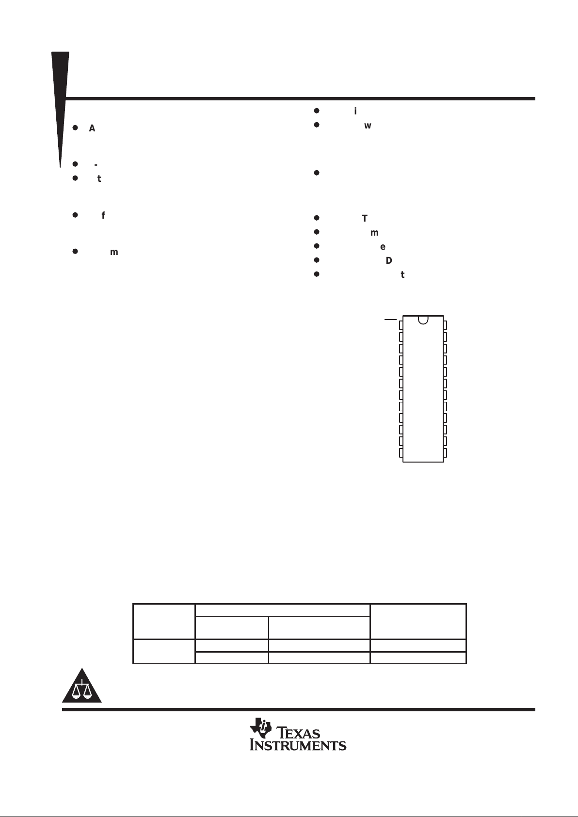
1
2
3
4
5
6
7
8
9
10
11
12
24
23
22
21
20
19
18
17
16
15
14
13
OE
DGND
D1(LSB)
D2
D3
D4
D5
D6
D7
D8(MSB)
V
DDD
CLK
DGND
REFB
REFBS
AGND
AGND
ANALOG IN
V
DDA
REFT
REFTS
V
DDA
V
DDA
V
DDD
PW OR NS PACKAGE
†
(TOP VIEW)
†
Available in tape and reel only and ordered
as the shown in the Available Options table
below.
TLC5510, TLC5510A
8-BIT HIGH-SPEED ANALOG-TO-DIGITAL CONVERTERS
SLAS095K – SEPTEMBER 1994 – REVISED MA Y 1999
2
POST OFFICE BOX 655303 • DALLAS, TEXAS 75265
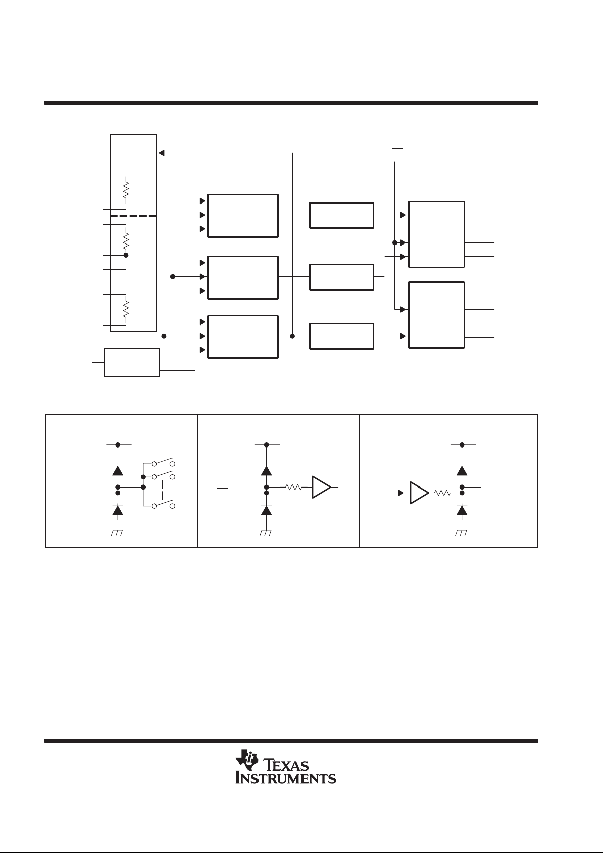
functional block diagram
Lower Sampling
Comparators
(4-Bit)
Lower Encoder
(4-Bit)
Lower Data
Latch
Lower Sampling
Comparators
(4-Bit)
Lower Encoder
(4-Bit)
Upper Sampling
Comparators
(4-Bit)
Upper Encoder
(4-Bit)
Upper Data
Latch
Clock
Generator
OE
D1(LSB)
D2
D3
D4
D5
D6
D7
D8(MSB)
CLK
REFB
REFT
REFBS
AGND
AGND
ANALOG IN
V
DDA
REFTS
270 Ω
NOM
80 Ω
NOM
320 Ω
NOM
Resistor
Reference
Divider
schematics of inputs and outputs
EQUIVALENT OF ANALOG INPUT
V
DDA
AGND
ANALOG IN
EQUIVALENT OF EACH DIGITAL INPUT
V
DDD
DGND
OE, CLK
EQUIVALENT OF EACH DIGITAL OUTPUT
V
DDD
DGND
D1–D8
TLC5510, TLC5510A
8-BIT HIGH-SPEED ANALOG-TO-DIGITAL CONVERTERS
SLAS095K – SEPTEMBER 1994 – REVISED MA Y 1999
3
POST OFFICE BOX 655303 • DALLAS, TEXAS 75265
Terminal Functions
TERMINAL
NAME NO.
I/O
DESCRIPTION
AGND 20, 21 Analog ground
ANALOG IN 19 I Analog input
CLK 12 I Clock input
DGND 2, 24 Digital ground
D1–D8 3–10 O Digital data out. D1 = LSB, D8 = MSB
OE 1 I Output enable. When OE = low, data is enabled. When OE = high, D1–D8 is in high-impedance state.
V
DDA
14, 15, 18 Analog supply voltage
V
DDD
11, 13 Digital supply voltage
REFB 23 I Reference voltage in bottom
REFBS 22 Reference voltage in bottom. When using the TLC5510 internal voltage divider to generate a nominal 2-V
reference, REFBS is shorted to REFB (see Figure 3). When using the TLC5510A, REFBS is connected to
ground.
REFT 17 I Reference voltage in top
REFTS 16 Reference voltage in top. When using the TLC5510 internal voltage divider to generate a nominal 2-V
reference, REFTS is shorted to REFT (see Figure 3). When using the TLC5510A, REFTS is connected to
V
DDA
.
absolute maximum ratings
†
Supply voltage, V
DDA
, V
DDD
7 V. . . . . . . . . . . . . . . . . . . . . . . . . . . . . . . . . . . . . . . . . . . . . . . . . . . . . . . . . . . . . . . . .
Reference voltage input range, V
REFT
, V
REFB
AGND to V
DDA
. . . . . . . . . . . . . . . . . . . . . . . . . . . . . . . . . . . . . . .
Analog input voltage range, V
I(ANLG)
AGND to V
DDA
. . . . . . . . . . . . . . . . . . . . . . . . . . . . . . . . . . . . . . . . . . . . . . .
Digital input voltage range, V
I(DGTL)
DGND to V
DDD
. . . . . . . . . . . . . . . . . . . . . . . . . . . . . . . . . . . . . . . . . . . . . . . .
Digital output voltage range, V
O(DGTL)
DGND to V
DDD
. . . . . . . . . . . . . . . . . . . . . . . . . . . . . . . . . . . . . . . . . . . . .
Operating free-air temperature range, T
A
–20°C to 75°C. . . . . . . . . . . . . . . . . . . . . . . . . . . . . . . . . . . . . . . . . . . .
Storage temperature range, T
stg
–55°C to 150°C. . . . . . . . . . . . . . . . . . . . . . . . . . . . . . . . . . . . . . . . . . . . . . . . . . .
†
Stresses beyond those listed under “absolute maximum ratings” may cause permanent damage to the device. These are stress ratings only, and
functional operation of the device at these or any other conditions beyond those indicated under “recommended operating conditions” is not
implied. Exposure to absolute-maximum-rated conditions for extended periods may affect device reliability.
recommended operating conditions
MIN NOM MAX UNIT
V
DDA
–AGND 4.75 5 5.25
Supply voltage
V
DDD
–AGND 4.75 5 5.25
V
AGND–DGND –100 0 100 mV
Reference input voltage (top), V
ref(T)
‡
TLC5510A V
REFB
+2 4 V
Reference input voltage (bottom), V
ref(B)
‡
TLC5510A 0 V
REFT
–4 V
Analog input voltage range, V
I(ANLG)
V
REFB
V
REFT
V
High-level input voltage, V
IH
4 V
Low-level input voltage, V
IL
1 V
Pulse duration, clock high, t
w(H)
(see Figure 1) 25 ns
Pulse duration, clock low, t
w(L)
(see Figure 1) 25 ns
‡
The reference voltage levels for the TLC5510 are derived through an internal resistor divider between V
DDA
and ground and therefore are not
derived from a separate external voltage source (see the electrical characteristics and text). For the 4 V input range of the TLC5510A, the
reference voltage is externally applied across the center divider resistor.
TLC5510, TLC5510A
8-BIT HIGH-SPEED ANALOG-TO-DIGITAL CONVERTERS
SLAS095K – SEPTEMBER 1994 – REVISED MA Y 1999
4
POST OFFICE BOX 655303 • DALLAS, TEXAS 75265
electrical characteristics at VDD = 5 V , V
REFT
= 2.5 V , V
REFB
= 0.5 V , f
(CLK)
= 20 MHz, TA = 25°C (unless
otherwise noted)
digital I/O
PARAMETER TEST CONDITIONS
†
MIN TYP MAX UNIT
I
IH
High-level input current VDD = MAX, VIH = V
DD
5
I
IL
Low-level input current VDD = MAX, VIL = 0 5
µ
A
I
OH
High-level output current OE = GND, VDD = MIN, VOH = VDD–0.5 V –1.5
I
OL
Low-level output current OE = GND, VDD = MIN, VOL = 0.4 V 2.5
mA
I
OZH
High-level high-impedance-state
output leakage current
OE = VDD, VDD = MAX VOH = V
DD
16
I
OZL
Low-level high-impedance-state
output leakage current
OE = VDD, VDD = MIN VOL = 0 16
µ
A
†
Conditions marked MIN or MAX are as stated in recommended operating conditions.
power
PARAMETER TEST CONDITIONS
†
MIN TYP MAX UNIT
I
DD
Supply current
f
(CLK)
= 20 MHz, National Television System Committee (NTSC)
ramp wave input, reference resistor dissipation is separate
18 27 mA
TLC5510 V
ref
= REFT – REFB = 2 V 5.2 7.5 10.5 mA
I
ref
Reference voltage current
TLC5510A V
ref
= REFT – REFB = 4 V 10.4 15 21 mA
†
Conditions marked MIN or MAX are as stated in recommended operating conditions.
static performance
PARAMETER TEST CONDITIONS
†
MIN TYP MAX UNIT
Self-bias (1), at REFB
0.57 0.61 0.65
Self-bias (2), REFT – REFB
Short REFB to REFBS
,
Short REFT to REFTS
1.9 2.02 2.15
V
Self-bias (3), at REFT Short REFB to AGND, Short REFT to REFTS 2.18 2.29 2.4
R
ref
Reference voltage resistor Between REFT and REFB 190 270 350 Ω
C
i
Analog input capacitance V
I(ANLG)
= 1.5 V + 0.07 V
rms
16 pF
f
= 20 MHz,
TA = 25°C ±0.4 ±0.75
TLC5510
(CLK)
,
VI = 0.5 V to 2.5 V
TA = –20°C to 75°C ±1
Integral nonlinearity (INL)
f
= 20 MHz,
TA = 25°C ±0.4 ±0.75
TLC5510A
(CLK)
,
VI = 0 to 4 V
TA = –20°C to 75°C ±1
f
= 20 MHz,
TA = 25°C ±0.3 ±0.5
LSB
TLC5510
(CLK)
,
VI = 0.5 V to 2.5 V
TA = –20°C to 75°C ±0.75
Differential nonlinearity (DNL)
f
= 20 MHz,
TA = 25°C ±0.3 ±0.5
TLC5510A
(CLK)
,
VI = 0 to 4 V
TA = –20°C to 75°C ±0.75
TLC5510 V
ref
= REFT – REFB = 2 V –18 –43 –68 mV
EZSZero-scale error
TLC5510A V
ref
= REFT – REFB = 4 V –36 –86 –136 mV
TLC5510 V
ref
= REFT – REFB = 2 V –20 0 20 mV
EFSFull-scale error
TLC5510A V
ref
= REFT – REFB = 4 V –40 0 40 mV
†
Conditions marked MIN or MAX are as stated in recommended operating conditions.
TLC5510, TLC5510A
8-BIT HIGH-SPEED ANALOG-TO-DIGITAL CONVERTERS
SLAS095K – SEPTEMBER 1994 – REVISED MA Y 1999
5
POST OFFICE BOX 655303 • DALLAS, TEXAS 75265
operating characteristics at VDD = 5 V , V
REFT
= 2.5 V , V
REFB
= 0.5 V , f
(CLK)
= 20 MHz, TA = 25°C (unless
otherwise noted)
PARAMETER TEST CONDITIONS MIN TYP MAX UNIT
TLC5510
p
V
I(ANLG)
= 0.5 V – 2.5 V 20 MSPS
f
conv
Maximum conversion rate
TLC5510A
f
I
=
1-kHz ramp
V
I(ANLG)
= 0 V – 4 V 20 MSPS
BW Analog input bandwidth At – 1 dB 14 MHz
t
d(D)
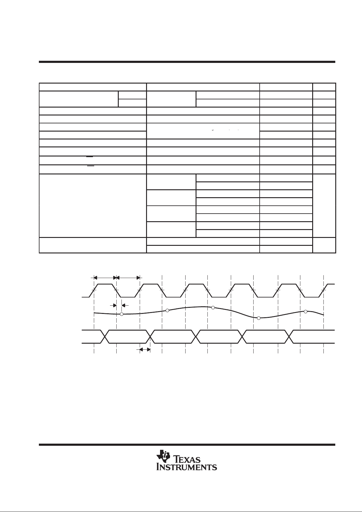
Digital output delay time CL ≤ 10 pF (see Note 1 and Figure 1) 18 30 ns
Differential gain
NTSC 40 Institute of Radio Engineers (IRE)
1%
Differential phase
g()
modulation wave, f
conv
= 14.3 MSPS
0.7 degrees
t
AJ
Aperture jitter time 30 ps
t
d(s)
Sampling delay time 4 ns
t
en
Enable time, OE↓ to valid data CL = 10 pF 5 ns
t
dis
Disable time, OE↑ to high impedance CL = 10 pF 7 ns
p
TA = 25°C 45
Input tone
= 1 MHz
Full range 43
p
TA = 25°C 45
p
Input tone
= 3 MHz
Full range 46
Spurious free dynamic range (SFDR)
p
TA = 25°C 43
dB
Input tone
= 6 MHz
Full range 42
p
TA = 25°C 39
Input tone
= 10 MHz
Full range 39
TA = 25°C 46
SNR
Signal-to-noise ratio
Full range 44
dB
NOTE 1: CL includes probe and jig capacitance.
N
N+1
N+2
N+3
N+4
N–3 N–2 N–1 N N+1
t
d(D)
CLK (clock)
ANALOG IN
(input signal)
D1–D8
(output data)
t
w(H)
t
w(L)
t
d(s)
Figure 1. I/O Timing Diagram

TLC5510, TLC5510A
8-BIT HIGH-SPEED ANALOG-TO-DIGITAL CONVERTERS
SLAS095K – SEPTEMBER 1994 – REVISED MA Y 1999
6
POST OFFICE BOX 655303 • DALLAS, TEXAS 75265
PRINCIPLES OF OPERATION
functional description
The TLC5510 and TLC5510A are semiflash ADCs featuring two lower comparator blocks of four bits each.
As shown in Figure 2, input voltage V
I
(1) is sampled with the falling edge of CLK1 to the upper comparators block
and the lower comparators block(A), S(1). The upper comparators block finalizes the upper data UD(1) with the
rising edge of CLK2, and simultaneously, the lower reference voltage generates the voltage RV(1)
corresponding to the upper data. The lower comparators block (A) finalizes the lower data LD(1) with the rising
edge of CLK3. UD(1) and LD(1) are combined and output as OUT(1) with the rising edge of CLK4. As shown
in Figure 2, the output data is delayed 2.5 clocks from the analog input voltage sampling point.
Input voltage V
I
(2) is sampled with the falling edge of CLK2. UD(2) is finalized with the rising edge of CLK3, and
LD(2) is finalized with the rising edge of CLK4 at the lower comparators block(B). OUT(2) data appears with
the rising edge of CLK5.
VI(1) VI(2) VI(3) VI(4)
CLK1 CLK2 CLK3 CLK4
S(1) C(1) S(2) C(2) S(3) C(3) S(4) C(4)
S(1) H(1) C(1) S(3) H(3) C(3)
H(0) C(0) S(2) H(2) C(2) S(4) H(4)
LD(–2)
OUT(–2) OUT(–1) OUT(0) OUT(1)
ANALOG IN
(sampling points)
CLK (clock)
Upper Comparators Block
Upper Data
Lower Reference Voltage
Lower Comparators Block (A)
Lower Data (A)
Lower Comparators Block (B)
Lower Data (B)
D1–D8 (data output)
UD(0)
RV(0)
UD(1)
RV(1)
UD(2)
RV(2)
UD(3)
RV(3)
LD(–1)
LD(0)
LD(1)
LD(2)
CLK5
Figure 2. Internal Functional Timing Diagram

TLC5510, TLC5510A
8-BIT HIGH-SPEED ANALOG-TO-DIGITAL CONVERTERS
SLAS095K – SEPTEMBER 1994 – REVISED MA Y 1999
7
POST OFFICE BOX 655303 • DALLAS, TEXAS 75265
PRINCIPLES OF OPERATION
internal referencing
TLC5510
The three internal resistors shown with V
DDA
can generate a 2-V reference voltage. These resistors are brought
out on V
DDA
, REFTS, REFT, REFB, REFBS, and AGND.
T o use the internally generated reference voltage, terminal connections should be made as shown in Figure 3.
This connection provides the standard video 2-V reference for the nominal digital output.
R1
320 Ω NOM
R
ref
270 Ω NOM
R2
80 Ω NOM
V
DDA
(analog supply)
REFTS
REFT
REFB
REFBS
AGND
TLC5510
16
17
22
21
23
18
Figure 3. External Connections for a 2-V Analog Input Span Using the Internal-Reference Resistor Divider
TLC5510A
For an analog input span of 4 V , 4 V is supplied to REFT , and REFB is grounded and terminal connections should
be made as shown in Figure 4. This connection provides the 4-V reference for the nominal zero to full-scale
digital output with a 4 V
pp
analog input at ANALOG IN.
R1
320 Ω NOM
R
ref
270 Ω NOM
R2
80 Ω NOM
REFTS
REFT
REFB
REFBS
AGND
TLC5510A
16
17
22
21
23
18
4 V
V
DDA
(analog supply)
Figure 4. External Connections for 4-V Analog Input Span

TLC5510, TLC5510A
8-BIT HIGH-SPEED ANALOG-TO-DIGITAL CONVERTERS
SLAS095K – SEPTEMBER 1994 – REVISED MA Y 1999
8
POST OFFICE BOX 655303 • DALLAS, TEXAS 75265
PRINCIPLES OF OPERATION
functional operation
The output code change with input voltage is shown in Table 1.
Table 1. Functional Operation
INPUT SIGNAL
DIGITAL OUTPUT CODE
INPUT SIGNAL
VOLTAGE
STEP
MSB LSB
V
ref(B)
255 0 0 0 0 0 0 0 0
•
• • •••••••
• • ••••••••
• 128 0 1111111
• 127 1 0000000
• • • •••••••
• • ••••••••
V
ref(T)
0 1 1 1 1 1 1 1 1
APPLICATION INFORMATION
The following notes are design recommendations that should be used with the device.
D
External analog and digital circuitry should be physically separated and shielded as much as possible to
reduce system noise.
D
RF breadboarding or printed-circuit-board (PCB) techniques should be used throughout the evaluation and
production process. Breadboards should be copper clad for bench evaluation.
D
Since AGND and DGND are connected internally , the ground lead in must be kept as noise free as possible.
A good method to use is twisted-pair cables for the supply lines to minimize noise pickup. An analog and
digital ground plane should be used on PCB layouts when additional logic devices are used. The AGND
and DGND terminals of the device should be tied to the analog ground plane.
D
V
DDA
to AGND and V
DDD
to DGND should be decoupled with 1-µF and 0.01-µF capacitors, respectively ,
and placed as close as possible to the affected device terminals. A ceramic-chip capacitor is recommended
for the 0.01-µF capacitor. Care should be exercised to ensure a solid noise-free ground connection for the
analog and digital ground terminals.
D
V
DDA
, AGND, and ANALOG IN should be shielded from the higher frequency terminals, CLK and D0–D7.
When possible, AGND traces should be placed on both sides of the ANALOG IN traces on the PCB for
shielding.
D
In testing or application of the device, the resistance of the driving source connected to the analog input
should be 10 Ω or less within the analog frequency range of interest.

TLC5510, TLC5510A
8-BIT HIGH-SPEED ANALOG-TO-DIGITAL CONVERTERS
SLAS095K – SEPTEMBER 1994 – REVISED MA Y 1999
9
POST OFFICE BOX 655303 • DALLAS, TEXAS 75265
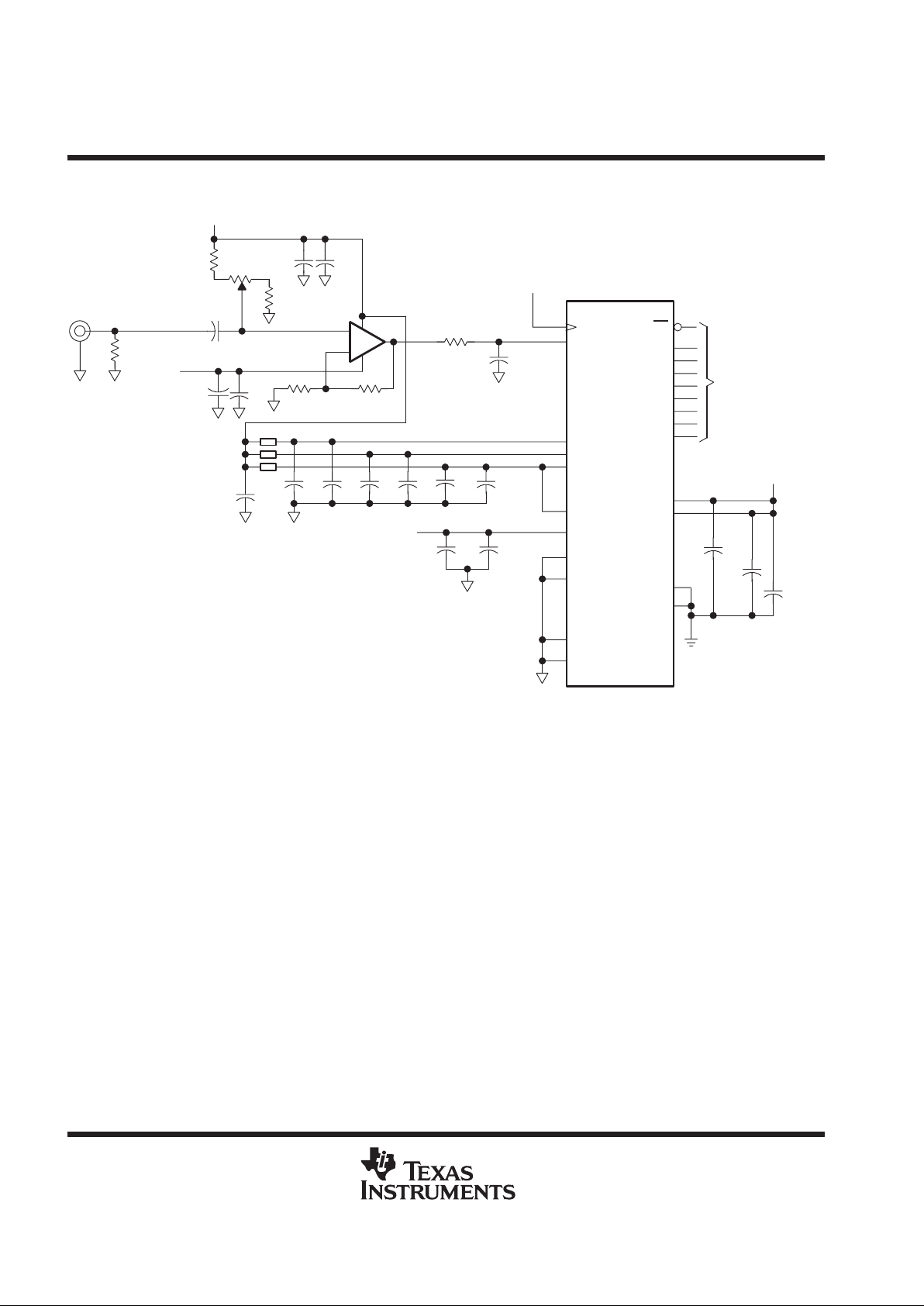
APPLICATION INFORMATION
C1
D1
C3
C4
C5
C6
C2
C11
C9
C7
C8
C10
C12
R5
R4 R2
R1
Q1
D3
D2
TP3
R3
C11
FB2
FB3
FB7
FB1
V
REF
ADJ
TP1
J1
V
DDD
V
DDA
V
DDA
REFTS
REFT
V
DDA
ANALOG IN
AGND
AGND
REFBS
REFB
DGND
12
11
10
9
8
7
6
5
4
3
2
1
13
14
15
16
17
18
19
20
21
22
23
24
CLK
V
DDD
D8 (MSB)
D7
D6
D5
D4
D3
D2
D1 (LSB)
DGND
OE
TLC5510
AV
DD
5 V
Clock
Output
Enable
DV
DD
5 V
Video
Input
JP2JP1
JP4JP3
– 5 V
NOTE A: Shorting JP1 and JP3 allows adjustment of the reference voltage by R5 using temperature-compensating diodes D2 and D3
which compensate for D1 and Q1 variations. By shorting JP2 and JP4, the internal divider generates a nominal 2-V reference.
LOCATION DESCRIPTION
C1, C3–C4, C6–C12 0.1-µF capacitor
C2 10-pF capacitor
C5 47-µF capacitor
FB1, FB2, FB3, FB7 Ferrite bead
Q1 2N3414 or equivalent
R1, R3 75-Ω resistor
R2 500-Ω resistor
R4 10-kΩ resistor, clamp voltage adjust
R5 300-Ω resistor, reference-voltage fine adjust
Figure 5. TLC5510 Evaluation and Test Schematic

TLC5510, TLC5510A
8-BIT HIGH-SPEED ANALOG-TO-DIGITAL CONVERTERS
SLAS095K – SEPTEMBER 1994 – REVISED MA Y 1999
10
POST OFFICE BOX 655303 • DALLAS, TEXAS 75265
APPLICATION INFORMATION
C1
D1
C3
C5
C6
C2
C11
C9
C7
C8
C4
R5
R4 R2
R1
Q1
R3
C11
FB2
FB3
FB7
FB1
V
REF
ADJ
TP1
J1
V
DDD
V
DDA
V
DDA
REFTS
REFT
V
DDA
ANALOG IN
AGND
AGND
REFBS
REFB
DGND
12
11
10
9
8
7
6
5
4
3
2
1
13
14
15
16
17
18
19
20
21
22
23
24
CLK
V
DDD
D8 (MSB)
D7
D6
D5
D4
D3
D2
D1 (LSB)
DGND
OE
TLC5510A
AV
DD
5 V
Clock
Output
Enable
DV
DD
5 V
Video
Input
– 5 V
NOTE A: R5 allows adjustment of the reference voltage to 4 V. R4 adjusts for the desired Q1 quiescent operating point.
LOCATION
DESCRIPTION
C1, C3–C4, C6–C11 0.1-µF capacitor
C2 10-pF capacitor
C5 47-µF capacitor
FB1, FB2, FB3, FB7 Ferrite bead
Q1 2N3414 or equivalent
R1, R3 75-Ω resistor
R2 500-Ω resistor
R4 10-kΩ resistor, clamp voltage adjust
R5 300-Ω resistor, reference-voltage fine adjust
Figure 6. TLC5510A Evaluation and Test Schematic

TLC5510, TLC5510A
8-BIT HIGH-SPEED ANALOG-TO-DIGITAL CONVERTERS
SLAS095K – SEPTEMBER 1994 – REVISED MA Y 1999
11
POST OFFICE BOX 655303 • DALLAS, TEXAS 75265
APPLICATION INFORMATION
CLOCK
CLOCK
ANALOG IN
OE
D1
D2
D3
D4
D5
D6
D7
D8
To Processor
100 pF
49.9 Ω
0.1 µF
4.7 µF
0.1 µF
+
4.7 µF
+
0.1 µF
4.7 µF
+
FB1
†
FB3
_
+
0.1 µF
+
4.7 µF
AV
SS
0.1 µF4.7 µF
+
1 kΩ
AV
DD
10 kΩ POT
1 kΩ
4.7 µF
49.9 Ω
V
DDA
V
DDA
V
DDA
REFTS
REFT
+
4.7 µF
0.1 µF
4.7 µF
+
REFBS
REFB
0.1 µF
4.7 µF
+
AGND
AGND
681 Ω
V
DDD
V
DDD
DGND
DGND
0.1 µF
0.1 µF
4.7 µF
DV
DD
TLC5510
THS3001
681 Ω
5 V
– 5V
†
FB – Ferrite Bead
5 V
Figure 7. TLC5510 Application Schematic
TLC5510, TLC5510A
8-BIT HIGH-SPEED ANALOG-TO-DIGITAL CONVERTERS
SLAS095K – SEPTEMBER 1994 – REVISED MA Y 1999
12
POST OFFICE BOX 655303 • DALLAS, TEXAS 75265
APPLICATION INFORMATION
CLOCK
CLOCK
ANALOG IN
OE
D1
D2
D3
D4
D5
D6
D7
D8
To Processor
100 pF
0.1 µF
4.7 µF
0.1 µF
+
4.7 µF
+
0.1 µF
4.7 µF
+
FB1
†
FB3
_
+
0.1 µF
+
4.7 µF
AV
SS
0.1 µF4.7 µF
+
1 kΩ
AV
DD
10 kΩ POT
1 kΩ
4.7 µF
49.9 Ω
V
DDA
V
DDA
V
DDA
REFTS
REFT
+
4.7 µF
REFBS
REFB
AGND
AGND
681 Ω
V
DDD
V
DDD
DGND
DGND
0.1 µF
0.1 µF
4.7 µF
DV
DD
V
ref
TLC5510A
AD8001
681 Ω
49.9 Ω
†
FB – Ferrite Bead
5 V
– 5 V
5 V
0.1 µF
4.7 µF
4 V
Figure 8. TLC5510A Application Schematic
TLC5510, TLC5510A
8-BIT HIGH-SPEED ANALOG-TO-DIGITAL CONVERTERS
SLAS095K – SEPTEMBER 1994 – REVISED MA Y 1999
13
POST OFFICE BOX 655303 • DALLAS, TEXAS 75265
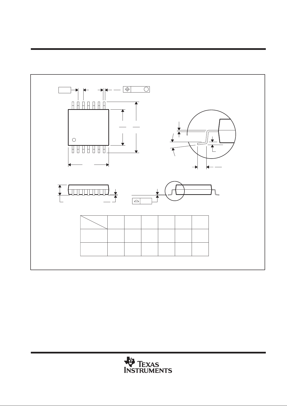
MECHANICAL DATA
PW (R-PDSO-G**) PLASTIC SMALL-OUTLINE PACKAGE
14 PINS SHOWN
0,65
M
0,10
0,10
0,25
0,50
0,75
0,15 NOM
Gage Plane
28
9,80
9,60
24
7,90
7,70
2016
6,60
6,40
4040064/F 01/97
0,30
6,60
6,20
8
0,19
4,30
4,50
7
0,15
14
A
1
1,20 MAX
14
5,10
4,90
8
3,10
2,90
A MAX
A MIN
DIM
PINS **
0,05
4,90
5,10
Seating Plane
0°–8°
NOTES: A. All linear dimensions are in millimeters.
B. This drawing is subject to change without notice.
C. Body dimensions do not include mold flash or protrusion not to exceed 0,15.
D. Falls within JEDEC MO-153
TLC5510, TLC5510A
8-BIT HIGH-SPEED ANALOG-TO-DIGITAL CONVERTERS
SLAS095K – SEPTEMBER 1994 – REVISED MA Y 1999
14
POST OFFICE BOX 655303 • DALLAS, TEXAS 75265
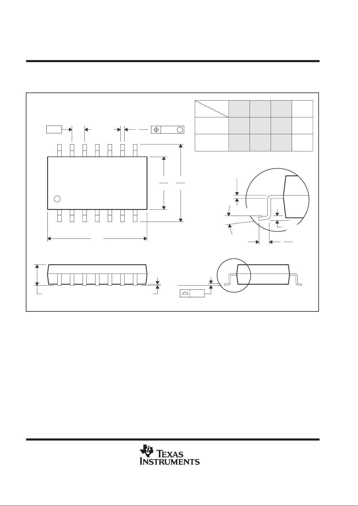
MECHANICAL DATA
NS (R-PDSO-G**) PLASTIC SMALL-OUTLINE PACKAGE
4040062/B 2/95
14 PIN SHOWN
2,00 MAX
A
0,05 MIN
Seating Plane
1,05
0,55
1
14
PINS **
5,60
5,00
7
8,20
7,40
8
A MIN
A MAX
DIM
Gage Plane
0,15 NOM
0,25
9,90 9,90
10,501410,50
16
12,30 14,70
15,3012,90
20 24
0,10
1,27
0°–10°
M
0,25
0,35
0,51
NOTES: A. All linear dimensions are in millimeters.
B. This drawing is subject to change without notice.
C. Body dimensions do not include mold flash or protrusion, not to exceed 0,15.

IMPORTANT NOTICE
T exas Instruments and its subsidiaries (TI) reserve the right to make changes to their products or to discontinue
any product or service without notice, and advise customers to obtain the latest version of relevant information
to verify, before placing orders, that information being relied on is current and complete. All products are sold
subject to the terms and conditions of sale supplied at the time of order acknowledgement, including those
pertaining to warranty, patent infringement, and limitation of liability.
TI warrants performance of its semiconductor products to the specifications applicable at the time of sale in
accordance with TI’s standard warranty. Testing and other quality control techniques are utilized to the extent
TI deems necessary to support this warranty. Specific testing of all parameters of each device is not necessarily
performed, except those mandated by government requirements.
CERT AIN APPLICATIONS USING SEMICONDUCTOR PRODUCTS MAY INVOLVE POTENTIAL RISKS OF
DEATH, PERSONAL INJURY, OR SEVERE PROPERTY OR ENVIRONMENTAL DAMAGE (“CRITICAL
APPLICATIONS”). TI SEMICONDUCTOR PRODUCTS ARE NOT DESIGNED, AUTHORIZED, OR
WARRANTED TO BE SUITABLE FOR USE IN LIFE-SUPPORT DEVICES OR SYSTEMS OR OTHER
CRITICAL APPLICATIONS. INCLUSION OF TI PRODUCTS IN SUCH APPLICA TIONS IS UNDERST OOD TO
BE FULLY AT THE CUSTOMER’S RISK.
In order to minimize risks associated with the customer’s applications, adequate design and operating
safeguards must be provided by the customer to minimize inherent or procedural hazards.
TI assumes no liability for applications assistance or customer product design. TI does not warrant or represent
that any license, either express or implied, is granted under any patent right, copyright, mask work right, or other
intellectual property right of TI covering or relating to any combination, machine, or process in which such
semiconductor products or services might be or are used. TI’s publication of information regarding any third
party’s products or services does not constitute TI’s approval, warranty or endorsement thereof.
Copyright 1999, Texas Instruments Incorporated
 Loading...