

TLC545C, TLC545I, TLC546C, TLC546I
8-BIT ANALOG-TO-DIGITAL CONVERTERS
WITH SERIAL CONTROL AND 19 INPUTS
SLAS066B – DECEMBER 1985 – REVISED OCTOBER 1996
1
POST OFFICE BOX 655303 • DALLAS, TEXAS 75265
D
8-Bit Resolution A/D Converter
D
Microprocessor Peripheral or Stand-Alone
Operation
D
On-Chip 20-Channel Analog Multiplexer
D
Built-in Self-Test Mode
D
Software-Controllable Sample and Hold
D
T otal Unadjusted Error...±0.5 LSB Max
D
Timing and Control Signals Compatible
With 8-Bit TLC540 and 10-Bit TLC1540 A/D
Converter Families
D
CMOS Technology
PARAMETER TL545
TL546
Channel Acquisition Time
Conversion Time (Max)
Sampling Rate (Max)
Power Dissipation (Max)
1.5 µs
9 µs
76 x 10
3
15 mW
2.7 µs
17 µs
40 x 10
3
15 mW
description
The TLC545 and TLC546 are CMOS
analog-to-digital converters built around an 8-bit
switched capacitor successive-approximation
analog-to-digital converter. They are designed for
serial interface to a microprocessor or peripheral
via a 3-state output with up to four control inputs
including independent SYSTEM CLOCK, I/O
CLOCK, chip select (CS
), and ADDRESS INPUT .
A 4-MHz system clock for the TLC545 and a
2.1-MHz system clock for the TLC546 with a
design that includes simultaneous read/write
operation allowing high-speed data transfers and
sample rates of up to 76,923 samples per second
for the TLC545, and 40,000 samples per second
for the TLC546.
In addition to the high-speed converter and
versatile control logic, there is an on-chip
20-channel analog multiplexer that can be used to
sample any one of 19 inputs or an internal self-test
voltage, and a sample-and-hold that can operate
automatically or under microprocessor control.
The converters incorporated in the TLC545 and TLC546 feature differential high-impedance reference inputs
that facilitate ratiometric conversion, scaling, and analog circuitry isolation from logic and supply noises. A totally
switched capacitor design allows low-error (±0.5 LSB) conversion in 9 µs for the TLC545, and 17 µs for the
TLC546, over the full operating temperature range.
Please be aware that an important notice concerning availability, standard warranty, and use in critical applications of
Texas Instruments semiconductor products and disclaimers thereto appears at the end of this data sheet.
Copyright 1996, Texas Instruments Incorporated
PRODUCTION DATA information is current as of publication date.
Products conform to specifications per the terms of Texas Instruments
standard warranty. Production processing does not necessarily include
testing of all parameters.
1
2
3
4
5
6
7
8
9
10
11
12
13
14
28
27
26
25
24
23
22
21
20
19
18
17
16
15
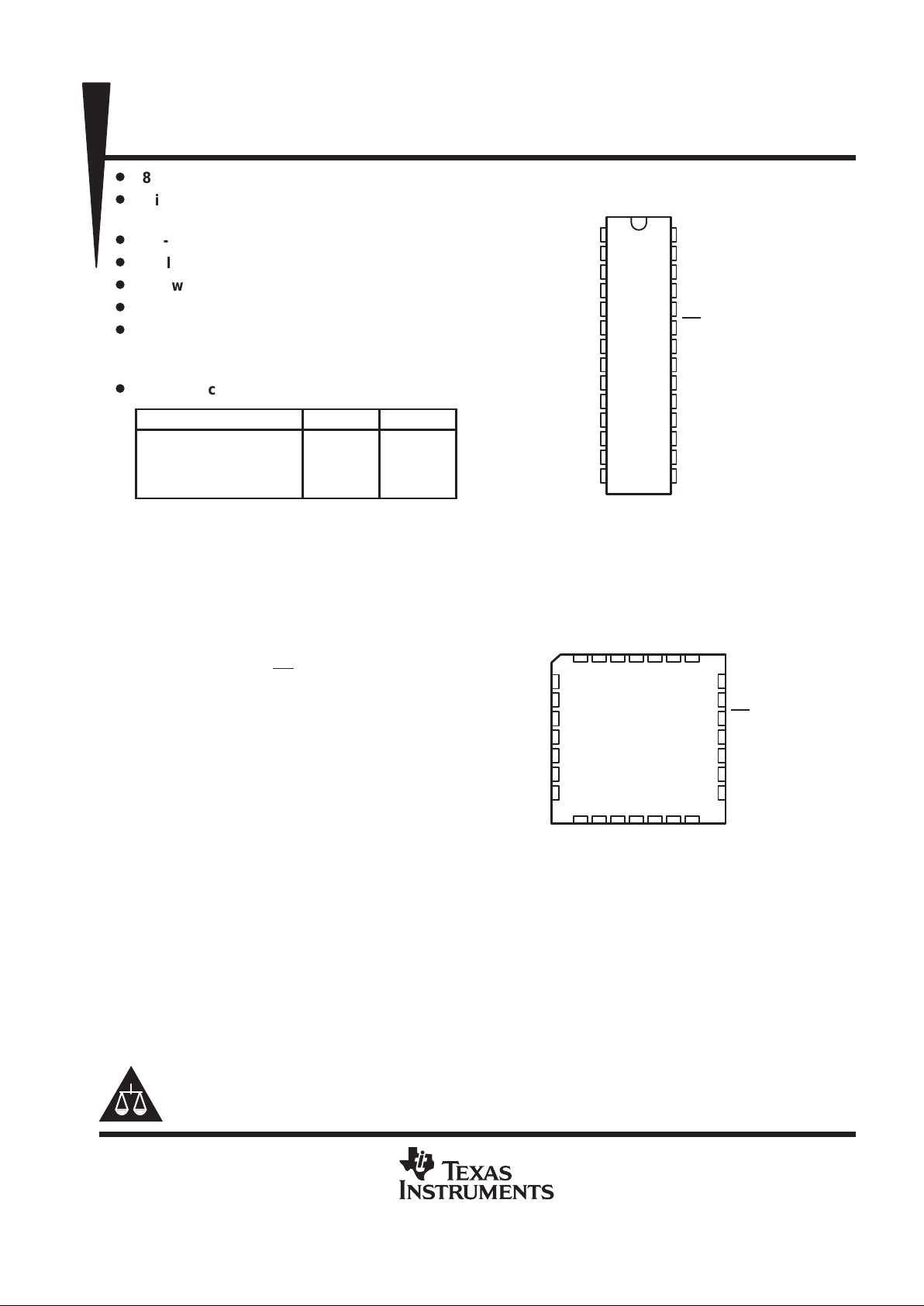
INPUT A0
INPUT A1
INPUT A2
INPUT A3
INPUT A4
INPUT A5
INPUT A6
INPUT A7
INPUT A8
INPUT A9
INPUT A10
INPUT A11
INPUT A12
GND
V
CC
SYSTEM CLOCK
I/O CLOCK
ADDRESS INPUT
DATA OUT
CS
REF+
REF–
INPUT A18
INPUT A17
INPUT A16
INPUT A15
INPUT A14
INPUT A13
N PACKAGE
(TOP VIEW)
321
13 14
5
6
7
8
9
10
11
ADDRESS INPUT
DATA OUT
CS
REF+
REF–
INPUT A18
INPUT A17
INPUT A4
INPUT A5
INPUT A6
INPUT A7
INPUT A8
INPUT A9
INPUT A10
4
15 16 17
18
INPUT A12
GND
INPUT A13
INPUT A14
INPUT A15
INPUT A16
INPUT A3
INPUT A2
INPUT A1
INPUT A0
FN PACKAGE
(TOP VIEW)
28 27 26
25
24
23
22
21
20
19
12
INPUT A1 1
V
SYSTEM CLOCK
I/O CLOCK
CC
TLC545C, TLC545I, TLC546C, TLC546I
8-BIT ANALOG-TO-DIGITAL CONVERTERS
WITH SERIAL CONTROL AND 19 INPUTS
SLAS066B – DECEMBER 1985 – REVISED OCTOBER 1996
2
POST OFFICE BOX 655303 • DALLAS, TEXAS 75265
AVAILABLE OPTIONS
PACKAGE
T
A
CHIP CARRIER
(FN)
PLASTIC DIP
(N)
0°C to 70°C
TLC545CFN
—
TLC545CN
—
–40°C to 85°C
TLC545IFN
TLC546IFN
TLC545IN
TLC546IN
description (continued)
The TLC545C and the TLC546C are characterized for operation from 0°C to 70°C. The TLC545I and the
TLC546I are characterized for operation from –40°C to 85°C.
functional block diagram
1
2
3
4
5
6
7
8
9
10
11
12
13
15
16
17
18
19
20
SYSTEM
CLOCK
CS
I/O
CLOCK
ADDRESS
INPUT
8-Bit
Analog-to-Digital
Converter
(Switched-capacitors)
8
4
2
5
5
8
REF–REF+
DATA
OUT
8-to-1 Data
Selector and
Driver
Control Logic
and I/O
Counters
Output
Data
Register
Input
Multiplexer
Self-Test
Reference
Input
Address
Register
Sample
and
Hold
20-Channel
Analog
Multiplexer
INPUTS
A0
A1
A2
A3
A4
A5
A6
A7
A8
A9
A10
A11
A12
A13
A14
A15
A16
A17
A18
25
26
23
27
22 21
24
TLC545C, TLC545I, TLC546C, TLC546I
8-BIT ANALOG-TO-DIGITAL CONVERTERS
WITH SERIAL CONTROL AND 19 INPUTS
SLAS066B – DECEMBER 1985 – REVISED OCTOBER 1996
3
POST OFFICE BOX 655303 • DALLAS, TEXAS 75265
typical equivalent inputs
INPUT CIRCUIT IMPEDANCE DURING SAMPLING MODE INPUT CIRCUIT IMPEDANCE DURING HOLD MODE
1 kΩ TYP
Ci = 60 pF TYP
(equivalent input
capacitance)
5 MΩ TYP
INPUT
A0–A18
INPUT
A0–A18
operating sequence
Access
Cycle B
(see Note C)
B0B2 C4
t
wH(CS)
Don’t Care
B7
B0B1B2B3B4B5B6B7
C3 C2 C1 C0
LSBMSB
Conversion Data B
MSBMSB
LSB
Hi-Z State
Don’t Care
MSB
LSB
(see Note B)
MSB
Previous Conversion Data A
A7
A7 A6 A5 A4 A3 A2 A1 A0
LSB
B1B3
MSB
B4
Don’t
1
1
See Note A
t
conv
Sample Cycle B
88765432765432
I/O
CLOCK
CS
DATA
OUT
ADDRESS
INPUT
Care
Access
Cycle C
Sample
Cycle C
Hi-Z
State
NOTES: A. The conversion cycle, which requires 36 system clock periods, is initiated with the eighth I/O CLOCK↓ after CS↓ for the channel
whose address exists in memory at that time.
B. The most significant bit (MSB) will automatically be placed on the DAT A OUT bus after CS
is brought low. The remaining seven bits
(A6–A0) will be clocked out on the first seven I/O CLOCK falling edges.
C. To minimize errors caused by noise at the CS
input, the internal circuitry waits for three system clock cycles (or less) after a chip
select transition before responding to control input signals. Therefore, no attempt should be made to clock-in address data until the
minimum chip-select setup time has elapsed.

TLC545C, TLC545I, TLC546C, TLC546I
8-BIT ANALOG-TO-DIGITAL CONVERTERS
WITH SERIAL CONTROL AND 19 INPUTS
SLAS066B – DECEMBER 1985 – REVISED OCTOBER 1996
4
POST OFFICE BOX 655303 • DALLAS, TEXAS 75265
absolute maximum ratings over operating free-air temperature range (unless otherwise noted)
†
Supply voltage, V
CC
(see Note 1) 6.5 V. . . . . . . . . . . . . . . . . . . . . . . . . . . . . . . . . . . . . . . . . . . . . . . . . . . . . . . . . . .
Input voltage range, V
I
(any input) –0.3 V to V
CC
+0.3 V. . . . . . . . . . . . . . . . . . . . . . . . . . . . . . . . . . . . . . . . . . . . .
Output voltage range, V
O
–0.3 V to VCC +0.3 V. . . . . . . . . . . . . . . . . . . . . . . . . . . . . . . . . . . . . . . . . . . . . . . . . . . .
Peak input current range (any input) ±10 mA. . . . . . . . . . . . . . . . . . . . . . . . . . . . . . . . . . . . . . . . . . . . . . . . . . . . . . .
Peak total input current (all inputs) ±30 mA. . . . . . . . . . . . . . . . . . . . . . . . . . . . . . . . . . . . . . . . . . . . . . . . . . . . . . . .
Operating free-air temperature range, T
A
: TLC545C, TLC546C 0°C to 70°C. . . . . . . . . . . . . . . . . . . . . . . . . .
TLC545I, TLC546I –40°C to 85°C. . . . . . . . . . . . . . . . . . . . . . . . . .
Storage temperature range, T
stg
–65°C to 150°C. . . . . . . . . . . . . . . . . . . . . . . . . . . . . . . . . . . . . . . . . . . . . . . . . . .
Case temperature for 10 seconds, T
C
: FN package 260°C. . . . . . . . . . . . . . . . . . . . . . . . . . . . . . . . . . . . . . . . . .
Lead temperature 1,6 mm (1/16 inch) from case for 10 seconds: N package 260°C. . . . . . . . . . . . . . . . . . . . .
†
Stresses beyond those listed under “absolute maximum ratings” may cause permanent damage to the device. These are stress ratings only, and
functional operation of the device at these or any other conditions beyond those indicated under “recommended operating conditions” is not
implied. Exposure to absolute-maximum-rated conditions for extended periods may affect device reliability.
NOTE 1: All voltage values are with respect to network ground terminal.

TLC545C, TLC545I, TLC546C, TLC546I
8-BIT ANALOG-TO-DIGITAL CONVERTERS
WITH SERIAL CONTROL AND 19 INPUTS
SLAS066B – DECEMBER 1985 – REVISED OCTOBER 1996
5
POST OFFICE BOX 655303 • DALLAS, TEXAS 75265
recommended operating conditions
TLC545 TLC546
MIN NOM MAX MIN NOM MAX
UNIT
Supply voltage, V
CC
4.75 5 5.5 4.75 5 5.5 V
Positive reference voltage, V
ref+
(see Note 2) 0 VCCVCC +0.1 0 VCCVCC +0.1 V
Negative reference voltage, V
ref–
(see Note 3) –0.1 0 V
CC
–0.1 0 V
CC
V
Differential reference voltage, V
ref+
– V
ref–
(see Note 3) 0 VCCVCC +0.2 0 VCCVCC +0.2 V
Analog input voltage (see Note 3) 0 V
CC
0 V
CC
V
High-level control input voltage, V
IH
2 2 V
Low-level control input voltage, V
IL
0.8 0.8 V
Setup time, address bits at data input before I/O CLOCK↑,
t
su(A)
200 400 ns
Address hold time, t
h
0 0 ns
Setup time, CS low before clocking in first address bit, t
su(CS)
(see Note 2)
3 3
System
clock
cycles
I/O CLOCK frequency, f
clock(I/O)
0 2.048 0 1.1 MHz
SYSTEM CLOCK frequency, f
clock(SYS)
f
clock(I/O)
4 f
clock(I/O)
2.1 MHz
Pulse duration, CS high during conversion, t
wH(CS)
36 36
System
clock
cycles
Pulse duration, SYSTEM CLOCK high, t
wH(SYS)
110 210 ns
Pulse duration, SYSTEM CLOCK low, t
wL(SYS)
100 190 ns
Pulse duration, I/O CLOCK high, t
wH(I/O)
200 404 ns
Pulse duration, I/O CLOCK low, t
wL(I/O)
200 404 ns
f
clock(SYS)
≤ 1048 kHz 30 30
Clock transition time
System
f
clock(SYS)
> 1048 kHz 20 20
ns
(see Note 4)
f
clock(I/O)
≤ 525 kHz 100 100
I/O
f
clock(I/O)
> 525 kHz 40 40
ns
p
p
TLC545C, TLC546C 0 70 0 70
Operating free-air temperature, T
A
TLC545I, TLC546I –40 85 –40 85 °C
NOTES: 2. T o minimize errors caused by noise at CS, the internal circuitry waits for three system clock cycles (or less) after a chip select falling
edge or rising edge is detected before responding to control input signals. Therefore, no attempt should be made to clock-in address
data until the minimum chip select setup time has elapsed.
3. Analog input voltages greater than that applied to REF+ convert as all “1”s (1 1111111), while input voltages less than that applied
to REF– convert as all “0”s (00000000). As the differential reference voltage decreases below 4.75 V , the total unadjusted error tends
to increase.
4. This is the time required for the clock input signal to fall from VIH min to VIL max or to rise from VIL max to VIH min. In the vicinity
of normal room temperature, the devices function with input clock transition time as slow as 2 µs for remote data acquisition
applications where the sensor and the A/D converter are placed several feet away from the controlling microprocessor.

TLC545C, TLC545I, TLC546C, TLC546I
8-BIT ANALOG-TO-DIGITAL CONVERTERS
WITH SERIAL CONTROL AND 19 INPUTS
SLAS066B – DECEMBER 1985 – REVISED OCTOBER 1996
6
POST OFFICE BOX 655303 • DALLAS, TEXAS 75265
electrical characteristics over recommended operating temperature range,
V
CC
= V
ref+
= 4.75 V to 5.5 V, f
clock(I/O)
= 2.048 MHz for TLC545 or f
clock(I/O)
= 1.1 MHz for TLC546
(unless otherwise noted)
PARAMETER TEST CONDITIONS MIN TYP†MAX UNIT
V
OH
High-level output voltage (DATA OUT) VCC = 4.75 V , IOH = –360 µA 2.4 V
V
OL
Low-level output voltage VCC = 4.75 V , IOL = 3.2 mA 0.4 V
p
p
VO = VCC, CS at V
CC
10
IOZOff-state (high-impedance state) ouput current
VO = 0, CS at V
CC
–10
µ
A
I
IH
High-level input current VI = V
CC
0.005 2.5 µA
I
IL
Low-level input current VI = 0 –0.005 –2.5 µA
I
CC
Operating supply current CS at 0 V 1.2 2.5 mA
Selected channel at VCC,
Unselected channel at 0 V
0.4 1
Selected channel leakage current
Selected channel at 0 V ,
Unselected channel at V
CC
–0.4 –1
µ
A
ICC + I
ref
Supply and reference current V
ref+
= VCC, CS at 0 V 1.3 3 mA
p
p
Analog inputs 7 55
p
CiInput capacitance
Control inputs 5 15
pF
†
All typical values are at TA = 25°C.

TLC545C, TLC545I, TLC546C, TLC546I
8-BIT ANALOG-TO-DIGITAL CONVERTERS
WITH SERIAL CONTROL AND 19 INPUTS
SLAS066B – DECEMBER 1985 – REVISED OCTOBER 1996
7
POST OFFICE BOX 655303 • DALLAS, TEXAS 75265
operating characteristics over recommended operating free-air temperature range,
V
CC
= V
ref+
= 4.75 V to 5.5 V, f
clock(I/O)
= 2.048 MHz for TLC545 or 1.1 MHz for TLC546,
f
clock(SYS)
= 4 MHz for TLC545 or 2.1 MHz for TLC546
TLC545 TLC546
PARAMETER
TEST CONDITIONS
MIN TYP MAX MIN TYP MAX
UNIT
E
L
Linearity error See Note 5 ±0.5 ±0.5 LSB
E
ZS
Zero-scale error See Note 6 ±0.5 ±0.5 LSB
E
FS
Full-scale error See Note 6 ±0.5 ±0.5 LSB
Total unadjusted error See Note 7 ±0.5 ±0.5 LSB
Self-test output code
INPUT A19 address = 10011
(see Note 8)
01111101
(125)
10000011
(131)
01111101
(125)
10000011
(131)
t
conv
Conversion time See Operating Sequence 9 17 µs
Total access and
conversion time
See Operating Sequence 13 25 µs
t
acq
Channel acquisition time
(sample cycle)
See Operating Sequence 3 3
I/O
clock
cycles
t
v
Time output data remains
valid after I/O CLOCK↓
10 10 ns
t
d
Delay time, I/O CLOCK to
DATA OUT valid
300 400 ns
t
en
Output enable time
See Parameter
150 150 ns
t
dis
Output disable time
See Parameter
Measurement Information
150 150 ns
t
r(bus)
Data bus rise time 300 300 ns
t
f(bus)
Data bus fall time 300 300 ns
NOTES: 5. Linearity error is the maximum deviation from the best straight line through the A/D transfer characteristics.
6. Zero-scale error is the difference between 00000000 and the converted output for zero input voltage; full-scale error is the difference
between 11111111 and the converted output for full-scale input voltage.
7. Total unadjusted error is the sum of linearity, zero-scale, and full-scale errors.
8. Both the input address and the output codes are expressed in positive logic. The INPUT A19 analog input signal is internally
generated and is used for test purposes.

TLC545C, TLC545I, TLC546C, TLC546I
8-BIT ANALOG-TO-DIGITAL CONVERTERS
WITH SERIAL CONTROL AND 19 INPUTS
SLAS066B – DECEMBER 1985 – REVISED OCTOBER 1996
8
POST OFFICE BOX 655303 • DALLAS, TEXAS 75265
PARAMETER MEASUREMENT INFORMATION
See Note B
0.4 V
2.4 V
t
f
Output
t
r
0.8 V
2.4 V
0.8 V
t
d
DATA OUT
VOLTAGE WAVEFORMS FOR RISE AND FALL TIMES
VOLTAGE WAVEFORMS FOR DELAY TIME
V
CC
3 kΩ
3 kΩ
V
CC
See Note B
SYSTEM
CLOCK
50%
50%
0 V
0 V
t
PLZ
I/O CLOCK
VOLTAGE WAVEFORMS FOR ENABLE AND DISABLE TIMES
Output Waveform 1
(see Note C)
t
PHZ
t
PZH
V
OH
90%
10%
t
PZL
0 V
V
CC
50%
CS
LOAD CIRCUIT FOR
t
PZL
AND t
PLZ
LOAD CIRCUIT FOR
t
PZH
AND t
PHZ
LOAD CIRCUIT FOR
td, tr, AND t
f
See Note B
C
L
(see Note A)
Output
Under Test
Test
Point
3 kΩ
1.4 V
Output Waveform 2
(see Note C)
C
L
(see Note A)
Output
Under Test
Test
Point
C
L
(see Note A)
Output
Under Test
Test
Point
NOTES: A. CL = 50 pF for TLC545 and 100 pF for TLC546
B. ten = t
PZH
or t
PZL
, t
dis
= t
PHZ
or t
PLZ
C. Waveform 1 is for an output with internal conditions such that the output is low except when disabled by the output control.
Waveform 2 is for an output with internal conditions such that the output is high except when disabled by the output control.

TLC545C, TLC545I, TLC546C, TLC546I
8-BIT ANALOG-TO-DIGITAL CONVERTERS
WITH SERIAL CONTROL AND 19 INPUTS
SLAS066B – DECEMBER 1985 – REVISED OCTOBER 1996
9
POST OFFICE BOX 655303 • DALLAS, TEXAS 75265
PARAMETER MEASUREMENT INFORMATION
simplified analog input analysis
Using the equivalent circuit in Figure 1, the time required to charge the analog input capacitance from 0 to V
S
within 1/2 LSB can be derived as follows:
The capacitance charging voltage is given by
V
C
= VS 1–e
–t
c/RtCi
( )
(1)
where
R
t
= Rs + r
i
The final voltage to 1/2 LSB is given by
(2)V
C
(1/2 LSB) = VS – (VS/512)
Equating equation 1 to equation 2 and solving for time t
c
gives
V
S
–(VS/512) = VS 1–e
( )
(3)
–t
c/RtCi
and
t
c
(1/2 LSB) = Rt × Ci × ln(512) (4)
Therefore, with the values given the time for the analog input signal to settle is
(5)
t
c
(1/2 LSB) = (Rs + 1 kΩ) × 60 pF × ln(512)
This time must be less than the converter sample time shown in the timing diagrams.
VI= Input Voltage at INPUT A0–A18
VS= External Driving Source Voltage
Rs= Source Resistance
ri= Input Resistance
Ci= Input Capacitance
†
Driving source requirements:
• Noise and distortion for the source must be equivalent to the
resolution of the converter.
• Rs must be real at the input frequency.
R
s
r
i
V
S
V
C
50 pF MAX
1 kΩ MAX
Driving Source
†
TLC545/6
C
i
V
I
Figure 1. Equivalent Input Circuit Including the Driving Source

TLC545C, TLC545I, TLC546C, TLC546I
8-BIT ANALOG-TO-DIGITAL CONVERTERS
WITH SERIAL CONTROL AND 19 INPUTS
SLAS066B – DECEMBER 1985 – REVISED OCTOBER 1996
10
POST OFFICE BOX 655303 • DALLAS, TEXAS 75265
PRINCIPLES OF OPERATION
The TLC545 and TLC546 are both complete data acquisition systems on single chips. Each includes such functions
as system clock, sample and hold, 8-bit A/D converter, data and control registers, and control logic. For flexibility and
access speed, there are four control inputs; CS
, ADDRESS INPUT , I/O CLOCK, and SYSTEM CLOCK. These control
inputs and a TTL-compatible 3-state output facilitate serial communications with a microprocessor or microcomputer.
The TLC545 and TLC546 can complete conversions in a maximum of 9 and 17 µs respectively, while complete
input-conversion-output cycles can be repeated at a maximum of 13 and 25 µs, respectively.
The system clock and I/O clock are normally used independently and do not require any special speed or phase
relationships between them. This independence simplifies the hardware and software control tasks for the device.
Once a clock signal within the specification range is applied to the SYSTEM CLOCK input, the control hardware and
software need only be concerned with addressing the desired analog channel, reading the previous conversion result,
and starting the conversion by using the I/O CLOCK. SYSTEM CLOCK will drive the “conversion crunching” circuitry
so that the control hardware and software need not be concerned with this task.
When CS
is high, DA T A OUT is in a high-impedance condition, and ADDRESS INPUT and I/O CLOCK are disabled.
This feature allows each of these terminals, with the exception of CS
, to share a control logic point with their
counterpart terminals on additional A/D devices when additional TLC545/TLC546 devices are used. Thus, the above
feature serves to minimize the required control logic terminals when using multiple A/D devices.
The control sequence has been designed to minimize the time and effort required to initiate conversion and obtain
the conversion result. A normal control sequence is:
1. CS
is brought low. To minimize errors caused by noise at CS , the internal circuitry waits for two rising edges
and then a falling edge of the SYSTEM CLOCK after a CS
transition before the transition is recognized. The
MSB of the previous conversion result automatically appears on DATA OUT.
2. A new positive-logic multiplexer address is shifted in on the first five rising edges of I/O CLOCK. The MSB of
the address is shifted in first. The negative edges of these five I/O clocks shift out the second, third, fourth,
fifth, and sixth most significant bits of the previous conversion result. The on-chip sample and hold begins
sampling the newly addressed analog input after the fifth falling edge. The sampling operation basically
involves the charging of internal capacitors to the level of the analog input voltage.
3. Two clock cycles are then applied to I/O CLOCK and the seventh and eighth conversion bits are shifted out on
the negative edges of these clock cycles.
4. The final eighth clock cycle is applied to I/O CLOCK. The falling edge of this clock cycle completes the analog
sampling process and initiates the hold function. Conversion is then performed during the next 36 system
clock cycles. After this final I/O clock cycle, CS
must go high or the I/O CLOCK must remain low for at least 36
system clock cycles to allow for the conversion function.
CS
can be kept low during periods of multiple conversion. When keeping CS low during periods of multiple
conversion, special care must be exercised to prevent noise glitches on the I/O CLOCK line. If glitches occur on the
I/O CLOCK line, the I/O sequence between the microprocessor/controller and the device loses synchronization. Also,
if CS
is taken high, it must remain high until the end of conversion. Otherwise, a valid falling edge of CS causes a
reset condition, which aborts the conversion in progress.
A new conversion may be started and the ongoing conversion simultaneously aborted by performing steps 1 through
4 before the 36 system clock cycles occur. Such action yields the conversion result of the previous conversion and
not the ongoing conversion.

TLC545C, TLC545I, TLC546C, TLC546I
8-BIT ANALOG-TO-DIGITAL CONVERTERS
WITH SERIAL CONTROL AND 19 INPUTS
SLAS066B – DECEMBER 1985 – REVISED OCTOBER 1996
11
POST OFFICE BOX 655303 • DALLAS, TEXAS 75265
PRINCIPLES OF OPERATION
It is possible to connect SYSTEM CLOCK and I/O CLOCK together in special situations in which controlling circuitry
points must be minimized. In this case, the following special points must be considered in addition to the requirements
of the normal control sequence previously described.
1. The first two clocks are required for this device to recognize CS
is at a valid low level when the common clock
signal is used as an I/O CLOCK. When CS
is recognized by the device to be at a high level, the common clock
signal is used for the conversion clock also.
2. A low CS
must be recognized before the I/O CLOCK can shift in an analog channel address. The device
recognizes a CS
transition when the SYSTEM CLOCK terminal receives two positive edges and then a
negative edge. For this reason, after a CS
negative edge, the first two clock cycles do not shift in the address.
Also, upon shifting in the address, CS
must be raised after the eighth valid (10 total) I/O CLOCK. Otherwise,
additional common clock cycles are recognized as I/O CLOCKS and shift in an erroneous address.
For certain applications, such as strobing applications, it is necessary to start conversion at a specific point in time.
This device accommodates these applications. Although the on-chip sample and hold begins sampling upon the
negative edge of the fourth valid I/O clock cycle, the hold function is not initiated until the negative edge of the eighth
valid I/O clock cycle. Thus, the control circuitry can leave the I/O clock signal in its high state during the eighth valid
I/O clock cycle, until the moment at which the analog signal must be converted. The TLC545/546 continues sampling
the analog input until the eighth valid falling edge of the I/O clock. The control circuitry or software must then
immediately lower the I/O clock signal to initiate the hold function at the desired point in time and to start conversion.

TLC545C, TLC545I, TLC546C, TLC546I
8-BIT ANALOG-TO-DIGITAL CONVERTERS
WITH SERIAL CONTROL AND 19 INPUTS
SLAS066B – DECEMBER 1985 – REVISED OCTOBER 1996
12
POST OFFICE BOX 655303 • DALLAS, TEXAS 75265

IMPORTANT NOTICE
T exas Instruments and its subsidiaries (TI) reserve the right to make changes to their products or to discontinue
any product or service without notice, and advise customers to obtain the latest version of relevant information
to verify, before placing orders, that information being relied on is current and complete. All products are sold
subject to the terms and conditions of sale supplied at the time of order acknowledgement, including those
pertaining to warranty, patent infringement, and limitation of liability.
TI warrants performance of its semiconductor products to the specifications applicable at the time of sale in
accordance with TI’s standard warranty. Testing and other quality control techniques are utilized to the extent
TI deems necessary to support this warranty. Specific testing of all parameters of each device is not necessarily
performed, except those mandated by government requirements.
CERT AIN APPLICATIONS USING SEMICONDUCTOR PRODUCTS MAY INVOLVE POTENTIAL RISKS OF
DEATH, PERSONAL INJURY, OR SEVERE PROPERTY OR ENVIRONMENTAL DAMAGE (“CRITICAL
APPLICATIONS”). TI SEMICONDUCTOR PRODUCTS ARE NOT DESIGNED, AUTHORIZED, OR
WARRANTED TO BE SUITABLE FOR USE IN LIFE-SUPPORT DEVICES OR SYSTEMS OR OTHER
CRITICAL APPLICATIONS. INCLUSION OF TI PRODUCTS IN SUCH APPLICA TIONS IS UNDERST OOD TO
BE FULLY AT THE CUSTOMER’S RISK.
In order to minimize risks associated with the customer’s applications, adequate design and operating
safeguards must be provided by the customer to minimize inherent or procedural hazards.
TI assumes no liability for applications assistance or customer product design. TI does not warrant or represent
that any license, either express or implied, is granted under any patent right, copyright, mask work right, or other
intellectual property right of TI covering or relating to any combination, machine, or process in which such
semiconductor products or services might be or are used. TI’s publication of information regarding any third
party’s products or services does not constitute TI’s approval, warranty or endorsement thereof.
Copyright 1999, Texas Instruments Incorporated
 Loading...