

Texas Instruments TLC4502AMJGB, TLC4502AMJG, TLC4502AMFKB, TLC4502AMD, TLC4502AID Datasheet
...
TLC4501, TLC4501A, TLC4502, TLC4502A
FAMILY OF SELF-CALIBRATING (Self-Cal)
PRECISION CMOS RAIL-TO-RAIL OUTPUT OPERATIONAL AMPLIFIERS
SLOS221A – MA Y 1998 – REVISED JULY 1999
1
POST OFFICE BOX 655303 • DALLAS, TEXAS 75265
D
Self-Calibrates Input Offset Voltage to
40 µV Max
D
Low Input Offset Voltage Drift ...1 µV/°C
D
Input Bias Current ...1 pA
D
Open Loop Gain . . . 120 dB
D
Rail-To-Rail Output Voltage Swing
D
Stable Driving 1000 pF Capacitive Loads
D
Gain Bandwidth Product . . . 4.7 MHz
D
Slew Rate . . . 2.5 V/µs
D
High Output Drive Capability . . . ±50 mA
D
Calibration Time . . . 300 ms
D
Characterized From –55°C to 125°C
D
Available in Q-Temp Automotive
HighRel Automotive Applications
Configuration Control / Print Support
Qualification to Automotive Standards
description
The TLC4501 and TLC4502 are the highest precision CMOS single supply rail-to-rail operational amplifiers
available today. The input offset voltage is 10 µV typical and 40 µV maximum. This exceptional precision,
combined with a 4.7-MHz bandwidth, 2.5-V/µs slew rate, and 50-mA output drive, is ideal for multiple
applications including: data acquisition systems, measurement equipment, industrial control applications, and
portable digital scales.
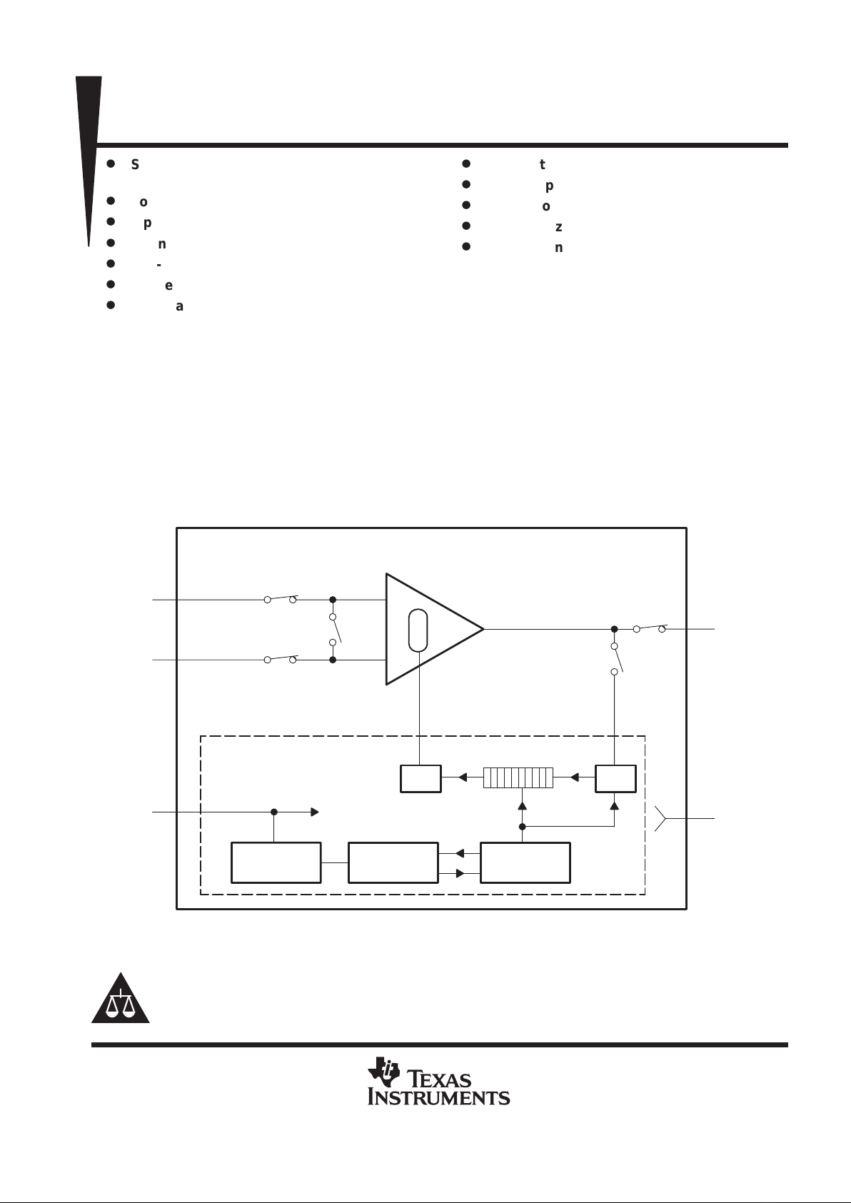
These amplifiers feature
self-calibrating
circuitry which digitally trims the input offset voltage to less than 40 µV
within the first 300 ms of operation. The offset is then digitally stored in an integrated successive approximation
register (SAR). Immediately after the data is stored, the calibration circuitry effectively drops out of the signal
path, shuts down, and the device functions as a standard operational amplifier.
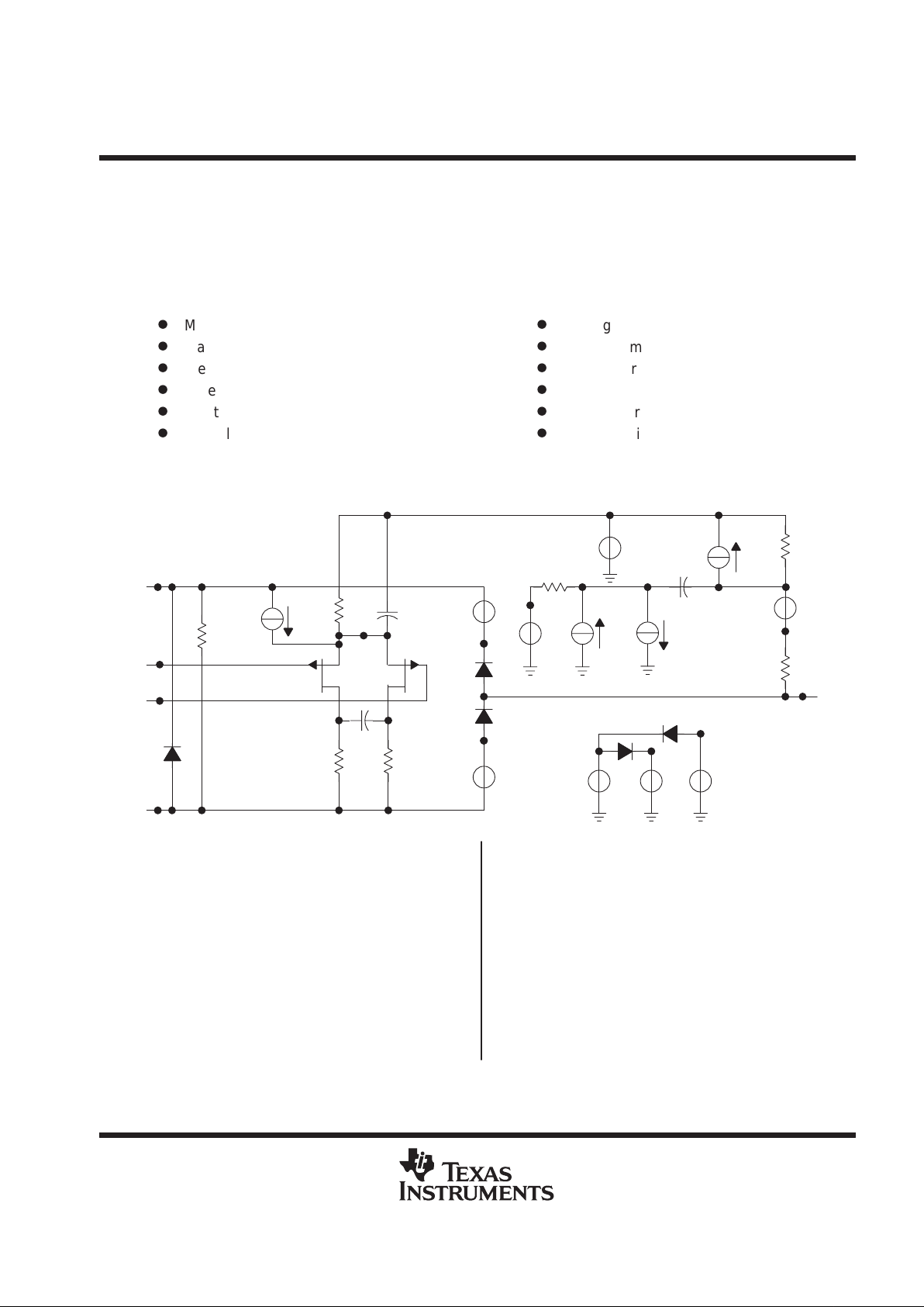
Power-On
Reset
IN+
OUT
A/D
–
+
Control
Logic
Oscillator
D/A
SAR
GND
IN–
V
DD
5 V
Calibration Circuitry
Offset Control
3
2
8
1
4
Figure 1. Channel One of the TLC4502
Please be aware that an important notice concerning availability, standard warranty, and use in critical applications of
Texas Instruments semiconductor products and disclaimers thereto appears at the end of this data sheet.
Copyright 1999, Texas Instruments Incorporated
PRODUCTION DATA information is current as of publication date.
Products conform to specifications per the terms of Texas Instruments
standard warranty. Production processing does not necessarily include
testing of all parameters.
LinEPIC and Self-Cal are trademarks of Texas Instruments Incorporated.
On products compliant to MIL-PRF-38535, all parameters are tested
unless otherwise noted. On all other products, production
processing does not necessarily include testing of all parameters.
TLC4501, TLC4501A, TLC4502, TLC4502A
FAMILY OF SELF-CALIBRATING (Self-Cal)
PRECISION CMOS RAIL-TO-RAIL OUTPUT OPERATIONAL AMPLIFIERS
SLOS221A – MA Y 1998 – REVISED JULY 1999
2
POST OFFICE BOX 655303 • DALLAS, TEXAS 75265
description (continued)
Using this technology eliminates the need for noisy and expensive chopper techniques, laser trimming, and
power hungry, split supply bipolar operational amplifiers.
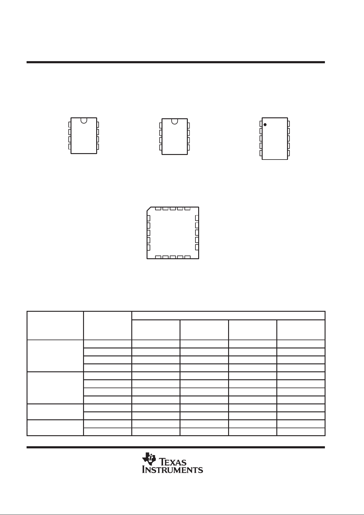
NC
V
DD
+
2OUT
2IN –
2IN +
NC
1OUT
1IN –
1IN +
V
DD–
/GND
1
2
3
4
5
10
9
8
7
6
3 2 1 20 19
910111213
4
5
6
7
8
18
17
16
15
14
NC
2OUT
NC
2IN–
NC
NC
1IN–
NC
1IN+
NC
NC
1OUT
NC
2IN+
NC
NC
NC
NC
V
DD+
V
DD–
/GND
TLC4502
FK PACKAGE
(TOP VIEW)
NC – No internal connection
1
2
3
4
8
7
6
5
1OUT
1IN –
1IN +
V
DD –
/GND
VDD+
2OUT
2IN–
2IN+
TLC4502
D OR JG PACKAGE
(TOP VIEW)
1
2
3
4
8
7
6
5
NC
1IN –
1IN +
V
DD –
/GND
NC
V
DD
+
OUT
NC
TLC4501
D PACKAGE
(TOP VIEW)
TLC4502
U PACKAGE
(TOP VIEW)
AVAILABLE OPTIONS
PACKAGED DEVICES
T
A
VIOmax AT 25°C
SMALL
OUTLINE
†
(D)
CHIP CARRIER
(FK)
CERAMIC DIP
(JG)
CERAMIC FLAT
PACK
(U)
40 µV TLC4501ACD — — —
°
°
50 µV TLC4502ACD — — —
0°C to 70°C
80 µV TLC4501CD — — —
100 µV TLC4502CD — — —
40 µV TLC4501AID — — —
°
°
50 µV TLC4502AID — — —
–
40°C to 125°C
80 µV TLC4501ID — — —
100 µV TLC4502ID — — —
°
°
50 µV TLC4502AQD — — —
–
40°C to 125°C
100 µV TLC4502QD — — —
°
°
50 µV TLC4502AMD TLC4502AMFKB TLC4502AMJGB TLC4502AMUB
–
55°C to 125°C
100 µV TLC4502MD TLC4502MFKB TLC4502MJGB TLC4502MUB
†
The D package is also available taped and reeled.
TLC4501, TLC4501A, TLC4502, TLC4502A
FAMILY OF SELF-CALIBRATING (Self-Cal)
PRECISION CMOS RAIL-TO-RAIL OUTPUT OPERATIONAL AMPLIFIERS
SLOS221A – MA Y 1998 – REVISED JULY 1999
3
POST OFFICE BOX 655303 • DALLAS, TEXAS 75265
absolute maximum ratings over operating free-air temperature range (unless otherwise noted)
†
Supply voltage, V
DD+
(see Note 1) 7 V. . . . . . . . . . . . . . . . . . . . . . . . . . . . . . . . . . . . . . . . . . . . . . . . . . . . . . . . . . . .
Differential input voltage, VID (see Note 2) ±7 V. . . . . . . . . . . . . . . . . . . . . . . . . . . . . . . . . . . . . . . . . . . . . . . . . . . .
Input voltage range, V
I
(any input, see Note 1) –0.3 V to 7 V. . . . . . . . . . . . . . . . . . . . . . . . . . . . . . . . . . . . . . . . .
Input current, II (each input) ±5 mA. . . . . . . . . . . . . . . . . . . . . . . . . . . . . . . . . . . . . . . . . . . . . . . . . . . . . . . . . . . . . . .
Output current, IO (each output) ±100 mA. . . . . . . . . . . . . . . . . . . . . . . . . . . . . . . . . . . . . . . . . . . . . . . . . . . . . . . . .
Total current into V
DD+
±100 mA. . . . . . . . . . . . . . . . . . . . . . . . . . . . . . . . . . . . . . . . . . . . . . . . . . . . . . . . . . . . . . . . .
Total current out of V
DD–
/GND ±100 mA. . . . . . . . . . . . . . . . . . . . . . . . . . . . . . . . . . . . . . . . . . . . . . . . . . . . . . . . . .
Electrostatic discharge (ESD) > 2 kV. . . . . . . . . . . . . . . . . . . . . . . . . . . . . . . . . . . . . . . . . . . . . . . . . . . . . . . . . . . . .
Duration of short-circuit current at (or below) 25°C (see Note 3) unlimited. . . . . . . . . . . . . . . . . . . . . . . . . . . . . .
Continuous total power dissipation See Dissipation Rating Table. . . . . . . . . . . . . . . . . . . . . . . . . . . . . . . . . . . . .
Operating free-air temperature range, T
A
: TLC4502C 0°C to 70°C. . . . . . . . . . . . . . . . . . . . . . . . . . . . . . . . . . . .
TLC4502I –40°C to 125°C. . . . . . . . . . . . . . . . . . . . . . . . . . . . . . . . . .
TLC4502Q –40°C to 125°C. . . . . . . . . . . . . . . . . . . . . . . . . . . . . . . . .
TLC4502M –55°C to 125°C. . . . . . . . . . . . . . . . . . . . . . . . . . . . . . . . .
Storage temperature range, T
stg
–65°C to 150°C. . . . . . . . . . . . . . . . . . . . . . . . . . . . . . . . . . . . . . . . . . . . . . . . . . .
Case temperature for 60 seconds, TC: FK package 260°C. . . . . . . . . . . . . . . . . . . . . . . . . . . . . . . . . . . . . . . . . .
Lead temperature 1,6 mm (1/16 inch) from case for 10 seconds 260°C. . . . . . . . . . . . . . . . . . . . . . . . . . . . . . .
†
Stresses beyond those listed under “absolute maximum ratings” may cause permanent damage to the device. These are stress ratings only, and
functional operation of the device at these or any other conditions beyond those indicated under “recommended operating conditions” is not
implied. Exposure to absolute-maximum-rated conditions for extended periods may affect device reliability.
NOTES: 1. All voltage values, except differential voltages, are with respect to V
DD –
/GND.
2. Differential voltages are at IN+ with respect to IN–. Excessive current flows when an input is brought below V
DD–
– 0.3 V.
3. The output may be shorted to either supply. Temperature and/or supply voltages must be limited to ensure that the maximum
dissipation rating is not exceeded.
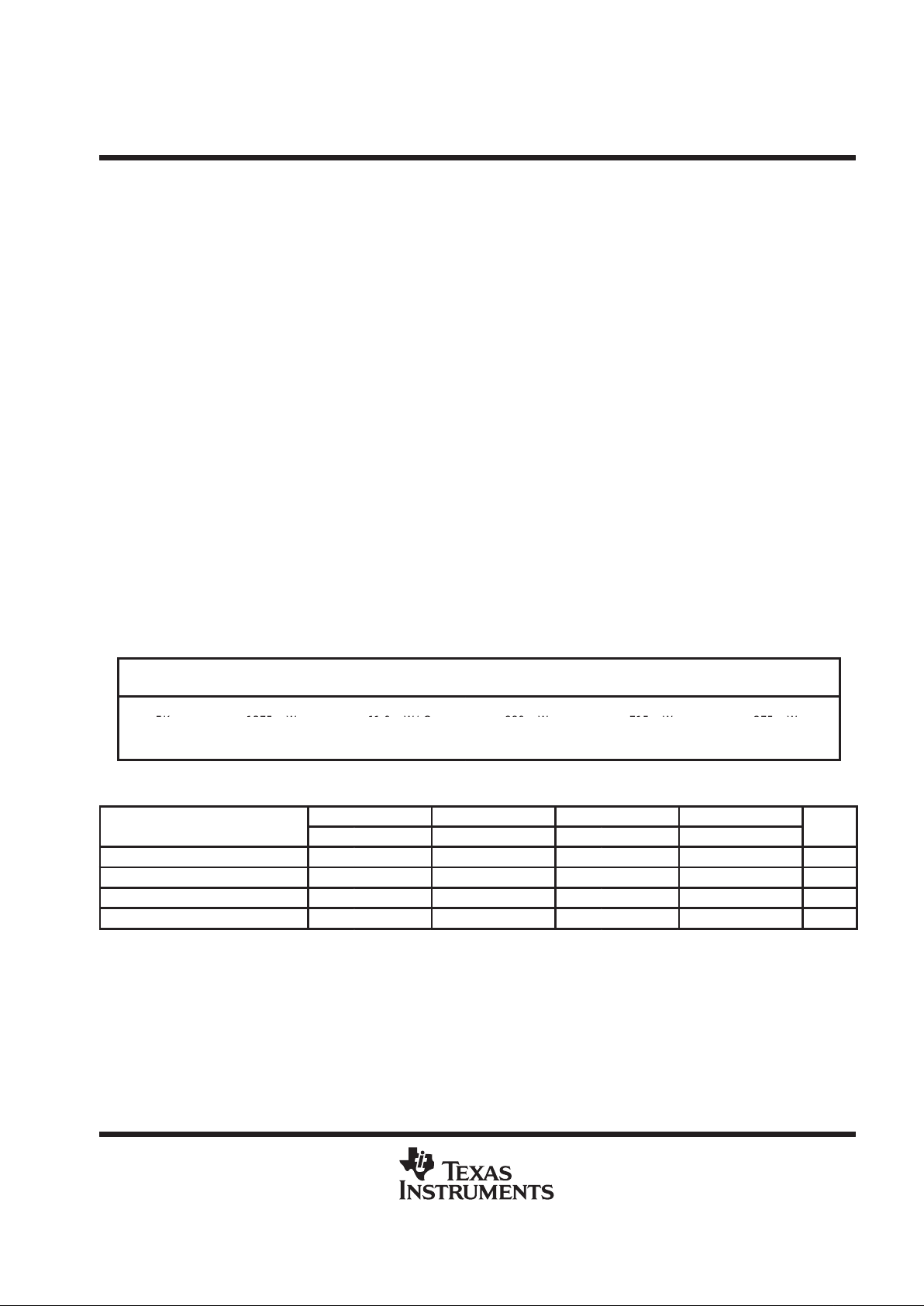
DISSIPATION RATING TABLE
T
≤ 25°C DERATING FACTOR T
= 70°C T
= 85°C T
= 125°C
PACKAGE
A
POWER RATING ABOVE TA = 25°CAPOWER RATINGAPOWER RATINGAPOWER RATING
D
725 mW
5.8 mW/°C
464 mW
377 mW
145 mW
FK
1375 mW
11.0 mW/°C
°
880 mW
715 mW
275 mW
JGU1050 mW
675 mW
8.4 mW/ C
5.4 mW/°C
672 mW
432 mW
546 mW
350 mW
210 mW
135 mW
recommended operating conditions
TLC4502C TLC4502I TLC4502Q TLC4502M
MIN MAX MIN MAX MIN MAX MIN MAX
UNIT
Supply voltage, V
DD
4 6 4 6 4 6 4 6 V
Input voltage range, V
I
V
DD–VDD+
– 2.3 V
DD–VDD+
– 2.3 V
DD–VDD+
– 2.3 V
DD–VDD+
– 2.3 V
Common-mode input voltage, V
IC
V
DD–VDD+
– 2.3 V
DD–VDD+
– 2.3 V
DD–VDD+
– 2.3 V
DD–VDD+
– 2.3 V
Operating free-air temperature, T
A
0 70 –40 125 –40 125 –55 125 °C
TLC4501, TLC4501A, TLC4502, TLC4502A
FAMILY OF SELF-CALIBRATING (Self-Cal)
PRECISION CMOS RAIL-TO-RAIL OUTPUT OPERATIONAL AMPLIFIERS
SLOS221A – MA Y 1998 – REVISED JULY 1999
4
POST OFFICE BOX 655303 • DALLAS, TEXAS 75265
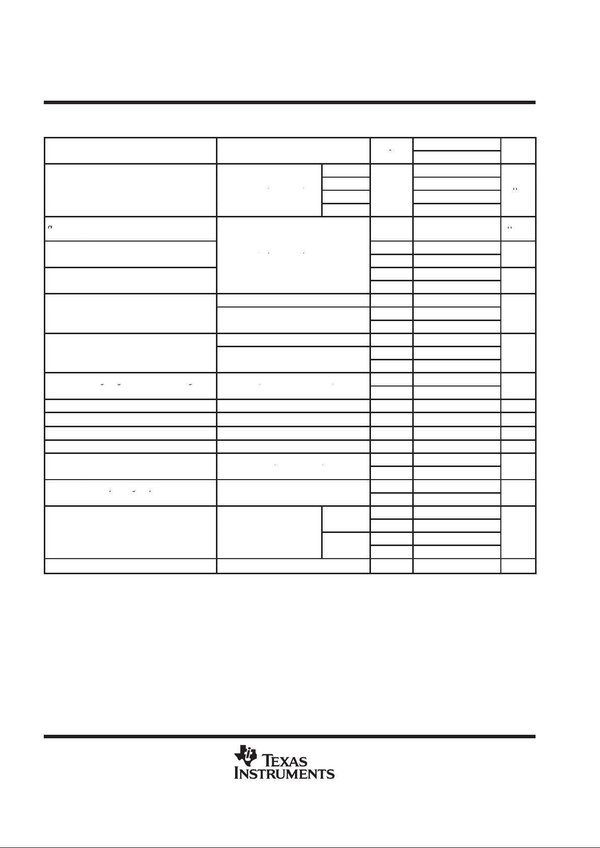
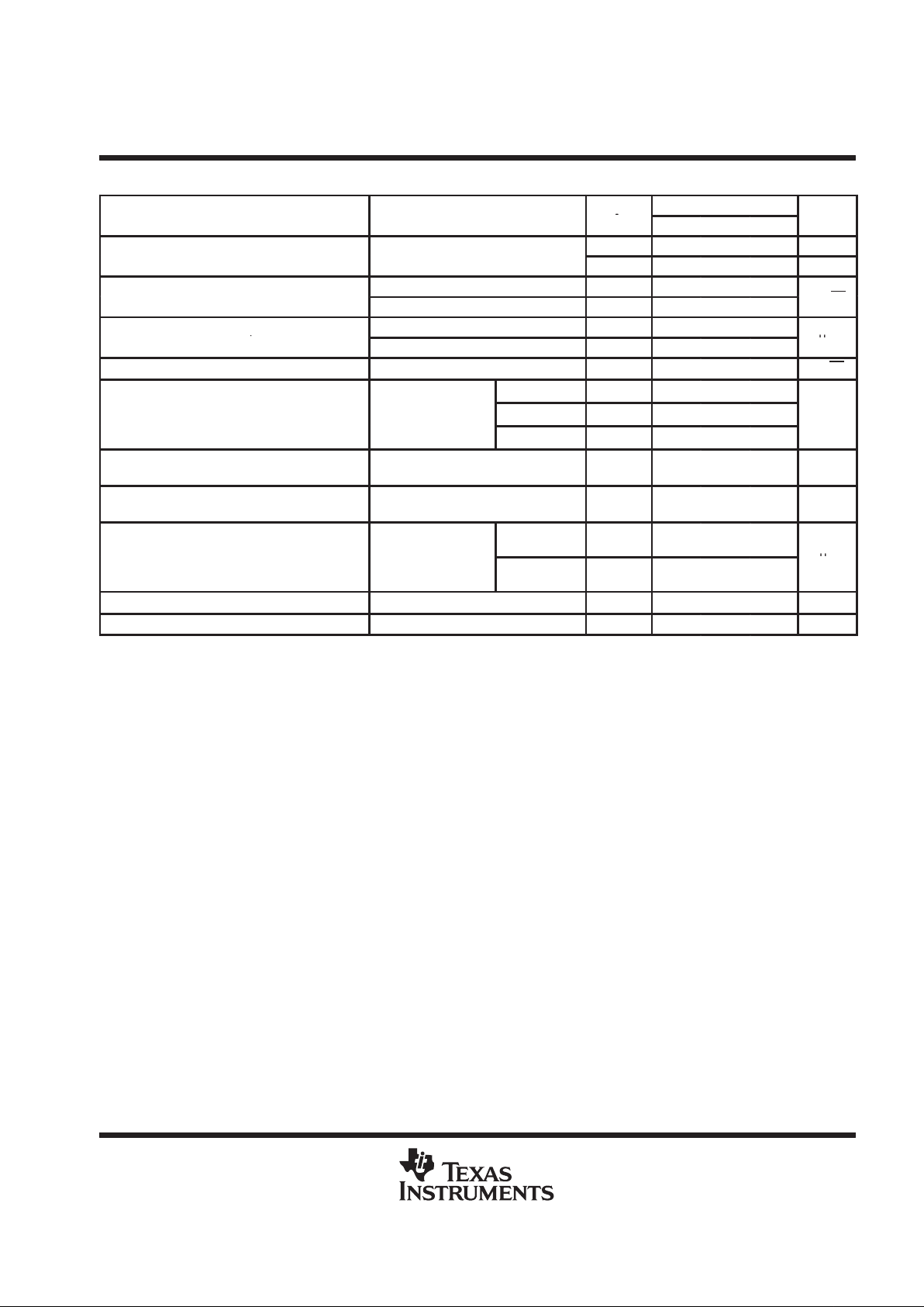
electrical characteristics at specified free-air temperature, VDD = 5 V, GND = 0 (unless otherwise
noted)
TLC450xC
PARAMETER
TEST CONDITIONS
T
A
†
MIN TYP MAX
UNIT
TLC4501 –80 10 80
p
V
= ±2.5 V , V
= 0,
TLC4501A
–40 10 40
VIOInput offset voltage
DD
,
VIC = 0,
O
,
RS = 50 Ω
TLC4502
Full range
–100 10 100
µ
V
TLC4502A –50 10 50
Temperature coefficient of input
°
α
VIO
offset voltage
Full range
1µV/°C
p
V
= ±2.5 V,V
= 0
,
25°C 1
p
IIOInput offset current
V
DD
±2.5 V,
VIC = 0,
V
O
0,
RS = 50 Ω
Full range 500
pA
p
25°C 1
p
IIBInput bias current
Full range 500
pA
IOH = – 500 µA 25°C 4.99
V
OH
High-level output voltage
25°C 4.9
V
I
OH
= – 5
mA
Full range 4.7
VIC = 2.5 V, IOL = 500 µA 25°C 0.01
V
OL
Low-level output voltage
25°C 0.1
V
V
IC
= 2.5 V,
I
OL
= 5
mA
Full range 0.3
Large-signal differential voltage V
= 2.5 V, V
= 1 V to 4 V,
25°C 200 1000
A
VD
gg g
amplification
IC
,
RL = 1 kΩ,
O
,
See Note 4
Full range
200
V/mV
R
I(D)
Differential input resistance 25°C 10 kΩ
R
L
Input resistance See Note 4 25°C
10
12
Ω
C
L
Common-mode input capacitance f = 10 kHz, P package 25°C 8 pF
z
O
Closed-loop output impedance AV = 10, f = 100 kHz 25°C 1 Ω
V
= 0 to 2.7 V, V
= 2.5 V,
25°C 90 100
CMRR
Common-mode rejection ratio
IC
,
O
,
RS = 1 kΩ
Full range 85
dB
Supply-voltage rejection ratio
25°C 90 100
k
SVR
ygj
(∆V
DD ±
/∆VIO)
V
DD
= 4 V to 6 V,
V
IC
= 0, No
load
Full range 90
dB
25°C 1 1.5
pp
TLC4501/A
Full range 2
IDDSupply current
V
O
= 2.5 V,
No load
25°C 2.5 3.5
mA
TLC4502/A
Full range 4
p
V
IT(CAL)
Calibration input threshold voltage
Full range
4
V
†
Full range is 0°C to 70°C.
NOTE 4: RL and CL values are referenced to 2.5 V .
TLC4501, TLC4501A, TLC4502, TLC4502A
FAMILY OF SELF-CALIBRATING (Self-Cal)
PRECISION CMOS RAIL-TO-RAIL OUTPUT OPERATIONAL AMPLIFIERS
SLOS221A – MA Y 1998 – REVISED JULY 1999
5
POST OFFICE BOX 655303 • DALLAS, TEXAS 75265
operating characteristics, VDD= 5 V
TLC450xC, TLC450xAC
PARAMETER
TEST CONDITIONS
T
A
†
MIN TYP MAX
UNIT
p
25°C 1.5 2.5 V/µs
SR
Slew rate at unity gain
V
O
= 0.5 V to 2.5 V,
C
L
=
100 pF
Full range 1 V/µs
p
f = 10 Hz
25°C 70
VnEquivalent input noise voltage
f = 1 kHz
25°C 12
n
V/√H
z
Peak-to-peak equivalent input noise
f = 0.1 to 1 Hz
25°C 1
V
N(PP)
q
voltage
f = 0.1 to 10 Hz
25°C 1.5
µ
V
I
n
Equivalent input noise current 25°C 0.6
fA/√Hz
VO = 0.5 V to 2.5 V,
AV = 1 25°C 0.02%
THD + N Total harmonic distortion plus noise
f = 10 kHz,
R
= 1 kΩ
,
AV = 10 25°C 0.08%
R
L
1 kΩ,
CL = 100 pF
AV = 100 25°C 0.55%
Gain-bandwidth product
f = 10 kHz,
CL = 100 pF
RL = 1 kΩ,
25°C 4.7 MHz
B
OM
Maximum output swing bandwidth
V
O(PP)
= 2 V,
RL = 1 kΩ,
AV = 1,
CL = 100 pF
25°C 1 MHz
AV = –1,
Step = 0.5 V to 2.5 V ,
to 0.1% 25°C 1.6
tsSettling time
RL = 1 kΩ,
CL = 100 pF
to 0.01% 25°C 2.2
µ
s
φ
m
Phase margin at unity gain RL = 1 kΩ, CL = 100 pF 25°C 74
Calibration time 25°C 300 ms
†
Full range is 0°C to 70°C.
NOTE 4: RL and CL values are referenced to 2.5 V .
TLC4501, TLC4501A, TLC4502, TLC4502A
FAMILY OF SELF-CALIBRATING (Self-Cal)
PRECISION CMOS RAIL-TO-RAIL OUTPUT OPERATIONAL AMPLIFIERS
SLOS221A – MA Y 1998 – REVISED JULY 1999
6
POST OFFICE BOX 655303 • DALLAS, TEXAS 75265
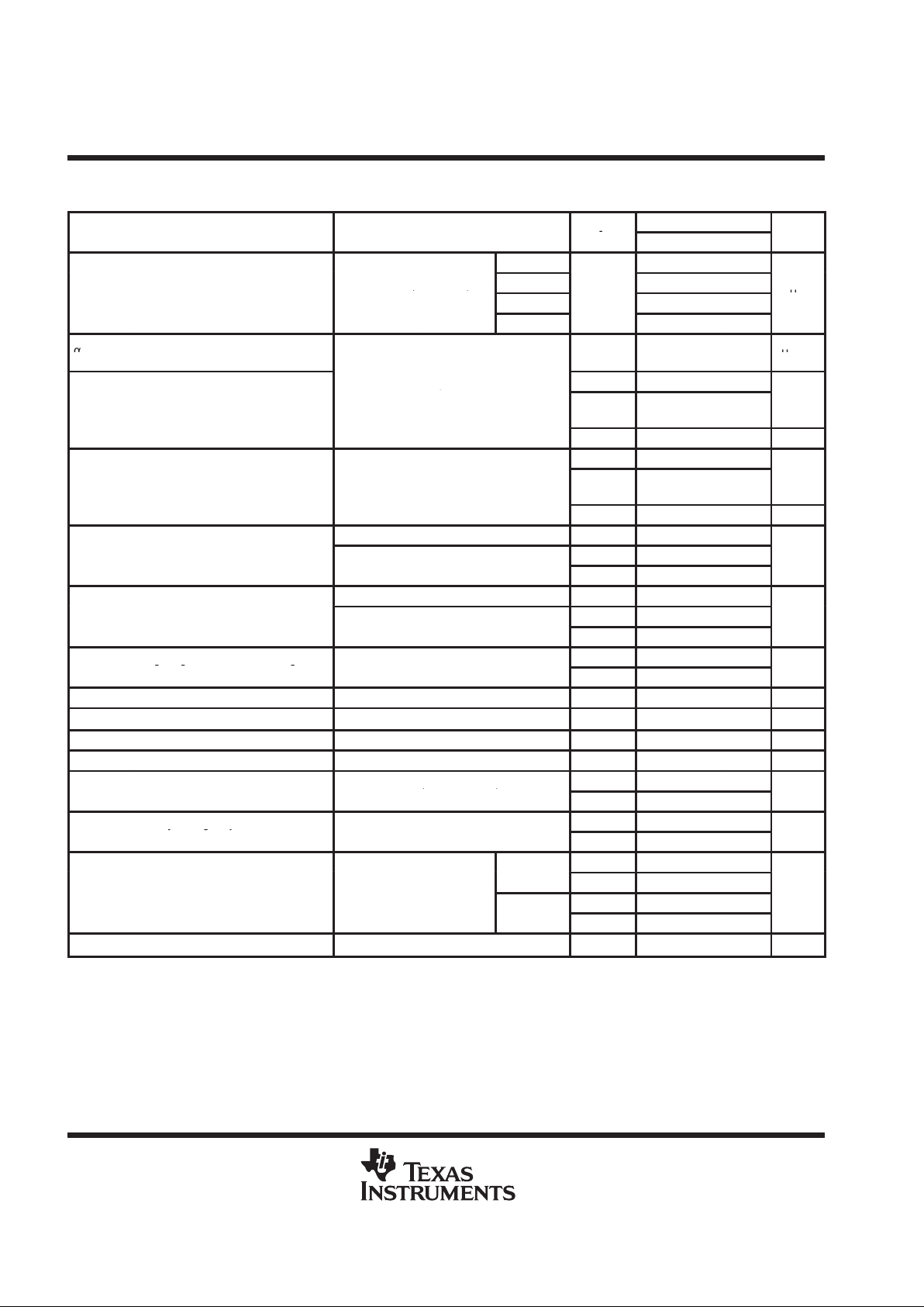
electrical characteristics at specified free-air temperature, VDD = 5 V, GND = 0 (unless otherwise
noted)
TLC450xI
PARAMETER
TEST CONDITIONS
T
A
†
MIN TYP MAX
UNIT
TLC4501 –80 10 80
p
V
= ±2.5 V , V
= 0,
TLC4501A
–40 10 40
VIOInput offset voltage
DD
,
VIC = 0,
O
,
RS = 50 Ω
TLC4502
Full range
–100 10 100
µ
V
TLC4502A –50 10 50
Temperature coefficient of input
°
α
VIO
offset voltage
Full range
1µV/°C
VDD = ±2.5 V , VO = 0,
25°C
1
I
IO
Input offset current
DD
VIC = 0,
O
RS = 50 Ω
–40°C to
85°C
500
pA
Full range 5 nA
25°C 1
I
IB
Input bias current
VDD = ±2.5 V ,
VIC = 0,
VO = 0,
RS = 50 Ω
–40°C to
85°C
500
pA
Full range 10 nA
IOH = – 500 µA 25°C 4.99
V
OH
High-level output voltage
25°C 4.9
V
I
OH
= – 5
mA
Full range 4.7
VIC = 2.5 V, IOL = 500 µA 25°C 0.01
V
OL
Low-level output voltage
25°C 0.1
V
V
IC
= 2.5 V,
I
OL
= 5
mA
Full range 0.3
Large-signal differential voltage V
= 2.5 V, V
= 1 V to 4 V,
25°C 200 1000
A
VD
gg g
amplification
IC
,
RL = 1 kΩ,
O
,
See Note 4
Full range
200
V/mV
R
I(D)
Differential input resistance 25°C 10 kΩ
R
L
Input resistance See Note 4 25°C
10
12
Ω
C
L
Common-mode input capacitance f = 10 kHz, P package 25°C 8 pF
z
O
Closed-loop output impedance AV = 10, f = 100 kHz 25°C 1 Ω
V
= 0 to 2.7 V, V
= 2.5 V,
25°C 90 100
CMRR
Common-mode rejection ratio
IC
,
O
,
RS = 1 kΩ
Full range 85
dB
Supply-voltage rejection ratio
25°C 90 100
k
SVR
ygj
(∆V
DD ±
/∆VIO)
V
DD
= 4 V to 6 V,
V
IC
= 0, No
load
Full range 90
dB
25°C 1 1.5
pp
TLC4501/A
Full range 2
IDDSupply current
V
O
= 2.5 V,
No load
25°C 2.5 3.5
mA
TLC4502/A
Full range 4
p
V
IT(CAL)
Calibration input threshold voltage
Full range
4
V
†
Full range is –40°C to 125°C.
NOTE 4: RL and CL values are referenced to 2.5 V .
TLC4501, TLC4501A, TLC4502, TLC4502A
FAMILY OF SELF-CALIBRATING (Self-Cal)
PRECISION CMOS RAIL-TO-RAIL OUTPUT OPERATIONAL AMPLIFIERS
SLOS221A – MA Y 1998 – REVISED JULY 1999
7
POST OFFICE BOX 655303 • DALLAS, TEXAS 75265
operating characteristics, VDD= 5 V
TLC450xI, TLC450xAI
PARAMETER
TEST CONDITIONS
T
A
†
MIN TYP MAX
UNIT
p
25°C 1.5 2.5 V/µs
SR
Slew rate at unity gain
V
O
= 0.5 V to 2.5 V,
C
L
=
100 pF
Full range 1 V/µs
p
f = 10 Hz
25°C 70
VnEquivalent input noise voltage
f = 1 kHz
25°C 12
n
V/√H
z
Peak-to-peak equivalent input noise
f = 0.1 to 1 Hz
25°C 1
V
N(PP)
q
voltage
f = 0.1 to 10 Hz
25°C 1.5
µ
V
I
n
Equivalent input noise current 25°C 0.6
fA/√Hz
VO = 0.5 V to 2.5 V,
AV = 1 25°C 0.02%
THD + N Total harmonic distortion plus noise
f = 10 kHz,
R
= 1 kΩ
,
AV = 10 25°C 0.08%
R
L
1 kΩ,
CL = 100 pF
AV = 100 25°C 0.55%
Gain-bandwidth product
f = 10 kHz,
CL = 100 pF
RL = 1 kΩ,
25°C 4.7 MHz
B
OM
Maximum output swing bandwidth
V
O(PP)
= 2 V,
RL = 1 kΩ,
AV = 1,
CL = 100 pF
25°C 1 MHz
AV = –1,
Step = 0.5 V to 2.5 V ,
to 0.1% 25°C 1.6
tsSettling time
RL = 1 kΩ,
CL = 100 pF
to 0.01% 25°C 2.2
µ
s
φ
m
Phase margin at unity gain RL = 1 kΩ, CL = 100 pF 25°C 74
Calibration time 25°C 300 ms
†
Full range is –40°C to 125°C.
NOTE 4: RL and CL values are referenced to 2.5 V .

TLC4501, TLC4501A, TLC4502, TLC4502A
FAMILY OF SELF-CALIBRATING (Self-Cal)
PRECISION CMOS RAIL-TO-RAIL OUTPUT OPERATIONAL AMPLIFIERS
SLOS221A – MA Y 1998 – REVISED JULY 1999
8
POST OFFICE BOX 655303 • DALLAS, TEXAS 75265
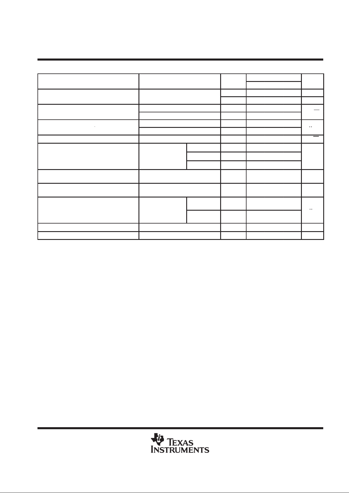
electrical characteristics at specified free-air temperature, VDD = 5 V, GND = 0 (unless otherwise
noted)
PARAMETER TEST CONDITIONS
T
†
TLC4502Q,
TLC4502M
UNIT
A
MIN TYP MAX
p
V
= ±2.5 V , V
= 0,
TLC4502
–100 10 100
VIOInput offset voltage
DD
,
VIC = 0,
O
,
RS = 50 Ω
TLC4502A
Full range
–50 10 50
µ
V
Temperature coefficient of input
°
α
VIO
offset voltage
Full range
1µV/°C
p
V
= ±2.5 V,V
= 0
,
25°C 1
IIOInput offset current
V
DD
±2.5 V,
VIC = 0,
V
O
0,
RS = 50 Ω
125°C
5
nA
p
25°C 1
IIBInput bias current
125°C 10
nA
IOH = – 500 µA 25°C 4.99
V
OH
High-level output voltage
25°C 4.9
V
I
OH
= – 5
mA
Full range 4.7
VIC = 2.5 V, IOL = 500 µA 25°C 0.01
V
OL
Low-level output voltage
25°C 0.1
V
V
IC
=
2.5 V
,
I
OL
=
5 mA
Full range 0.3
Large-signal differential voltage V
= 2.5 V, V
= 1 V to 4 V,
25°C 200 1000
A
VD
gg g
amplification
IC
,
RL = 1 kΩ,
O
,
See Note 4
Full range
200
V/mV
R
I(D)
Differential input resistance 25°C 10 kΩ
R
L
Input resistance See Note 4 25°C
10
12
Ω
C
L
Common-mode input capacitance f = 10 kHz, P package 25°C 8 pF
z
O
Closed-loop output impedance AV = 10, f = 100 kHz 25°C 1 Ω
V
= 0 to 2.7 V, V
= 2.5 V,
25°C 90 100
CMRR
Common-mode rejection ratio
IC
,
O
,
RS = 1 kΩ
Full range 85
dB
Supply-voltage rejection ratio V
= 4 V to 6 V, V
= V
/2,
25°C 90 100
k
SVR
ygj
(∆V
DD ±
/∆VIO)
DD
,
IC DD
,
No load
Full range 90
dB
pp
25°C 2.5 3.5
IDDSupply current
V
O
= 2.5 V,
No load
Full range 4
mA
p
V
IT(CAL)
Calibration input threshold voltage
Full range
4
V
†
Full range is –40°C to 125°C for Q suffix, –55°C to 125°C for M suffix.
NOTE 4: RL and CL values are referenced to 2.5 V .
TLC4501, TLC4501A, TLC4502, TLC4502A
FAMILY OF SELF-CALIBRATING (Self-Cal)
PRECISION CMOS RAIL-TO-RAIL OUTPUT OPERATIONAL AMPLIFIERS
SLOS221A – MA Y 1998 – REVISED JULY 1999
9
POST OFFICE BOX 655303 • DALLAS, TEXAS 75265
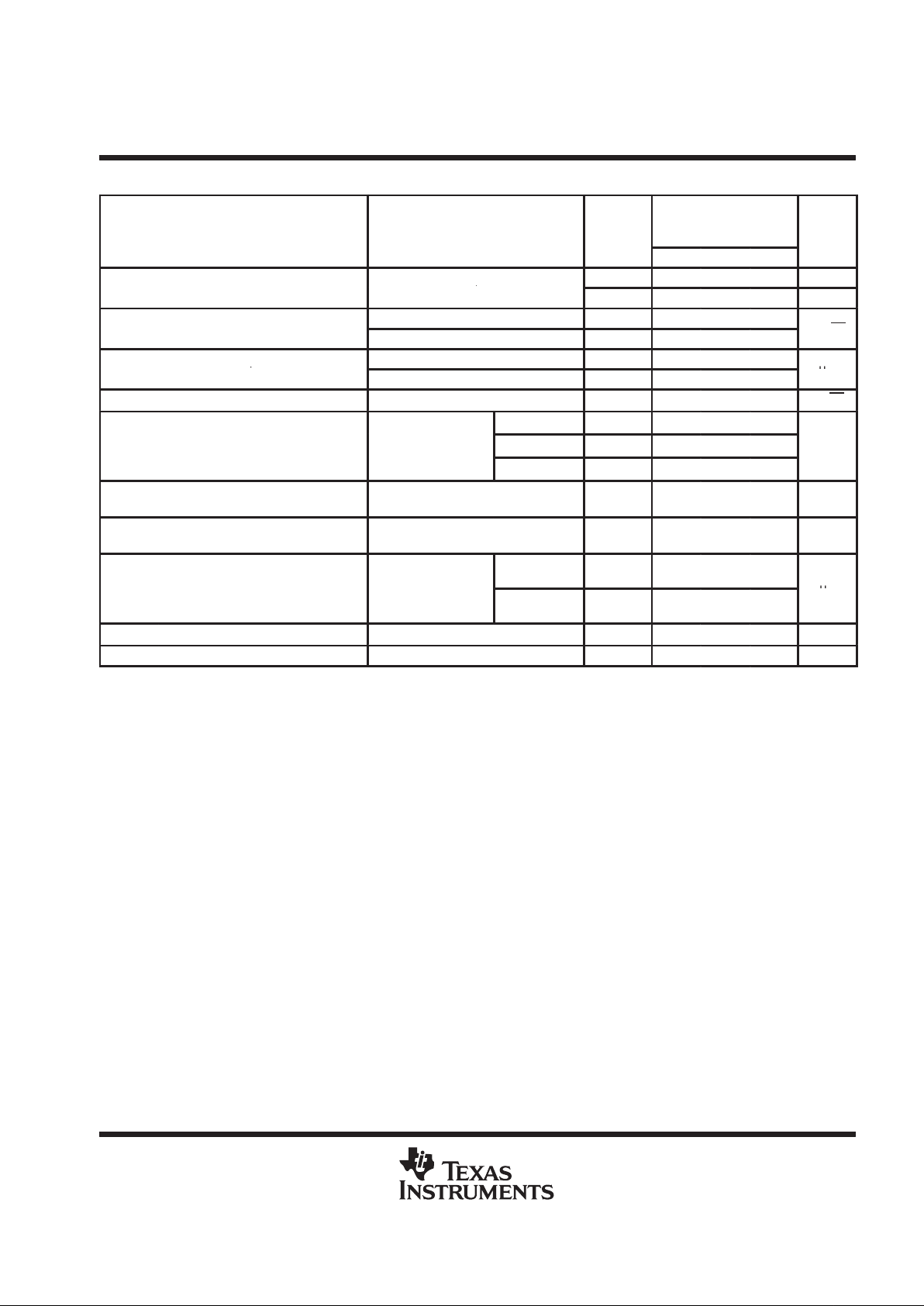
operating characteristics, VDD= 5 V
PARAMETER TEST CONDITIONS
T
A
†
TLC4502Q, TLC4502M,
TLC4502AQ,
TLC4502AM
UNIT
MIN TYP MAX
V
= 0.5 V to 2.5 V, C
= 100 pF
25°C 1.5 2.5 V/µs
SR
Slew rate at unity gain
O
,
See Note 4
L
Full range 1 V/µs
p
f = 10 Hz
25°C 70
VnEquivalent input noise voltage
f = 1 kHz
25°C 12
n
V/√H
z
Peak-to-peak equivalent input noise
f = 0.1 to 1 Hz
25°C 1
V
N(PP)
q
voltage
f = 0.1 to 10 Hz
25°C 1.5
µ
V
I
n
Equivalent input noise current 25°C 0.6
fA/√Hz
VO = 0.5 V to 2.5 V,
AV = 1 25°C 0.02%
THD + N Total harmonic distortion plus noise
f = 10 kHz,
R
= 1 kΩ
,
AV = 10 25°C 0.08%
R
L
1 kΩ,
CL = 100 pF
AV = 100 25°C 0.55%
Gain-bandwidth product
f = 10 kHz,
CL = 100 pF
RL = 1 kΩ,
25°C 4.7 MHz
B
OM
Maximum output swing bandwidth
V
O(PP)
= 2 V,
RL = 1 kΩ,
AV = 1,
CL = 100 pF
25°C 1 MHz
AV = –1,
Step = 0.5 V to 2.5 V ,
to 0.1% 25°C 1.6
tsSettling time
RL = 1 kΩ,
CL = 100 pF
to 0.01% 25°C 2.2
µ
s
φ
m
Phase margin at unity gain RL = 1 kΩ, CL = 100 pF 25°C 74
Calibration time 25°C 300 ms
†
Full range is –40°C to 125°C for Q suffix, –55°C to 125°C for M suffix.
NOTE 4: RL and CL values are referenced to 2.5 V .
TLC4501, TLC4501A, TLC4502, TLC4502A
FAMILY OF SELF-CALIBRATING (Self-Cal)
PRECISION CMOS RAIL-TO-RAIL OUTPUT OPERATIONAL AMPLIFIERS
SLOS221A – MA Y 1998 – REVISED JULY 1999
10
POST OFFICE BOX 655303 • DALLAS, TEXAS 75265
TYPICAL CHARACTERISTICS
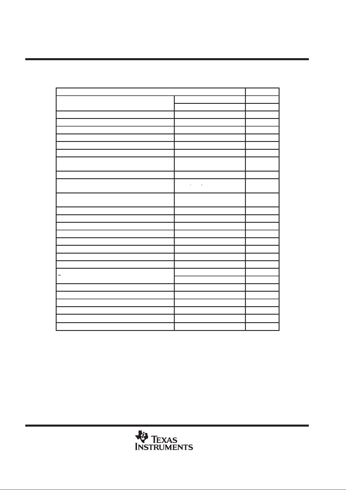
Table of Graphs
FIGURE
p
Distribution 2, 3, 4
VIOInput offset voltage
vs Common-mode input voltage 5
α
VIO
Input offset voltage temperature coefficient Distribution 6, 7
V
OH
High-level output voltage vs High-level output current 8
V
OL
Low-level output voltage vs Low-level output current 9
V
O(PP)
Maximum peak-to-peak output voltage vs Frequency 10
I
OS
Short-circuit output current vs Free-air temperature 11
V
O
Output voltage vs Differential input voltage 12
p
vs Free-air temperature 13
AVDLarge-signal differential voltage amplification
vs Frequency
14
z
o
Output impedance vs Frequency 15
vs Frequency 16
CMRR
Common-mode rejection ratio
qy
vs Free-air temperature 17
vs Load capacitance 18
SR
Slew rate
vs Free-air temperature 19
Inverting large-signal pulse response 20
Voltage-follower large-signal pulse response 21
Inverting small-signal pulse response 22
Voltage-follower small-signal pulse response 23
V
n
Equivalent input noise voltage vs Frequency 24
Input noise voltage Over a 10-second period 25
THD + N Total harmonic distortion plus noise vs Frequency 26
Gain-bandwidth product vs Free-air temperature 27
vs Load capacitance 28
φmPhase margin
vs Frequency 14
Gain margin vs Load capacitance 29
PSRR Power-supply rejection ratio vs Free-air temperature 30
Calibration time at –40°C 31
Calibration time at 25°C 32
Calibration time at 85°C 33
Calibration time at 125°C 34

TLC4501, TLC4501A, TLC4502, TLC4502A
FAMILY OF SELF-CALIBRATING (Self-Cal)
PRECISION CMOS RAIL-TO-RAIL OUTPUT OPERATIONAL AMPLIFIERS
SLOS221A – MA Y 1998 – REVISED JULY 1999
11
POST OFFICE BOX 655303 • DALLAS, TEXAS 75265
TYPICAL CHARACTERISTICS
10
8
2
0
12
16
DISTRIBUTION OF TLC4502 INPUT
OFFSET VOLTAGE
18
14
6
4
–40
–30
–20
–10
0
10
20
30
40
Percentage Of Amplification – %
VIO – Input Offset Voltage – µV
339 Amplifier From 2 Wafer Lot
VDD = ± 2.5 V
TA = 40°C
Figure 2
–60
6
4
2
0
10
12
14
–50
–40
–30
–20
–10
0
10
20
30
40
50
60
486 Amplifier From 8 Wafer Lot
VDD = ± 2.5 V
TA = 25°C
VIO – Input Offset Voltage – µV
Percentage of Amplifiers – %
DISTRIBUTION OF TLC4502 INPUT
OFFSET VOLTAGE
8
Figure 3
8
6
2
0
Percentage Of Amplification – %
10
12
DISTRIBUTION OF TLC4502 INPUT
OFFSET VOLTAGE
16
14
4
–50
–40
–30
–20
–10
0
10
20
30
40
50
VIO – Input Offset Voltage – µV
296 Amplifier From 2 Wafer Lot
VDD = ± 2.5 V
TA = 85°C
Figure 4 Figure 5
0
–50
–150
–200
–3 –2 –1 0
– Input Offset Voltage –
50
150
INPUT OFFSET VOLTAGE
vs
COMMON-MODE INPUT VOLTAGE
200
123
100
–100
VIC – Common-Mode Input Voltage – v
V
IO
Vµ
VDD = ±2.5 V
RS = 50 Ω
TA = 25°C

TLC4501, TLC4501A, TLC4502, TLC4502A
FAMILY OF SELF-CALIBRATING (Self-Cal)
PRECISION CMOS RAIL-TO-RAIL OUTPUT OPERATIONAL AMPLIFIERS
SLOS221A – MA Y 1998 – REVISED JULY 1999
12
POST OFFICE BOX 655303 • DALLAS, TEXAS 75265
TYPICAL CHARACTERISTICS
Figure 6
α
VIO
– Temperature Coefficient – µV/°C
30 Amplifiers From 1 Wafer Lot
VDD = ± 2.5 V
TA = 25°C To –40°C
10
5
0
–3 –2 0 1
Percentage Of Amplifiers – %
15
20
DISTRIBUTION OF TLC4502 INPUT OFFSET
VOLTAGE TEMPERATURE COEFFICIENT
25
23–1
Figure 7
30 Amplifiers From
1 Wafer Lot
VDD = ± 2.5 V
TA = 25°C To 85°C
10
8
2
0
Percentage Of Amplifiers – %
14
16
DISTRIBUTION OF TLC4502 INPUT OFFSET
VOLTAGE TEMPERATURE COEFFICIENT
20
18
12
6
4
–3.5–3–2.5–2–1.5–1–0.5
0
0.511.522.5
3
3.5
α
VIO
– Temperature Coefficient – µV/°C
Figure 8
IOH – High-Level Output Current – mA
3
2
0.5
0
010203040
3.5
4.5
HIGH-LEVEL OUTPUT VOLTAGE
vs
HIGH-LEVEL OUTPUT CURRENT
5
50 60 70 80
4
2.5
VDD = 5 V
VIC = 2.5 V
1.5
1
TA = –40°C
TA = 25°C
VOH – High-Level Output Voltage – V
V
OH
TA = 125°C
TA = 85°C
Figure 9
IOL – Low-Level Output Current – mA
1
0.75
0.25
0
0102030 4050
– Low-Level Output Voltage – V
1.5
1.75
LOW-LEVEL OUTPUT VOLTAGE
vs
LOW-LEVEL OUTPUT CURRENT
2
60 70 80
0.5
1.25
V
OL
VDD = 5 V
VIC = 2.5 V
TA = –40°C
TA = 25°C
TA = 85°C
TA = 125°C

TLC4501, TLC4501A, TLC4502, TLC4502A
FAMILY OF SELF-CALIBRATING (Self-Cal)
PRECISION CMOS RAIL-TO-RAIL OUTPUT OPERATIONAL AMPLIFIERS
SLOS221A – MA Y 1998 – REVISED JULY 1999
13
POST OFFICE BOX 655303 • DALLAS, TEXAS 75265
TYPICAL CHARACTERISTICS
Figure 10
8
4
2
0
10
6
100
– Maximum Peak-To-Peak Output Voltage – V
f – Frequency – Hz
MAXIMUM PEAK-TO-PEAK OUTPUT VOLTAGE
vs
FREQUENCY
1 k 10 k 100 k 1 M 10 M
V
O(PP)
VDD = 5 V
Figure 11
I
OS+
I
OS–
61
59
57
55
–50 –25 0 25
– Short-Circuit Output Current – mA
65
67
SHORT-CIRCUIT OUTPUT CURRENT
vs
FREE-AIR TEMPERATURE
69
50 75 100
63
TA – Free-Air Temperature – °C
I
OS
Figure 12
1
0
–2
–3
–0.2 –0.15 –0.1 –0.05
2
0.15
OUTPUT VOLTAGE
vs
DIFFERENTIAL INPUT VOLTAGE
0.20
3
–1
0.05 0.1
VID – Differential Input Voltage – mV
– Output Voltage – V
V
O
VDD = 5 V
VIC = 2.5 V
RL = 1 kΩ
TA = 25°C
Figure 13
800
600
200
0
–55 –30 –5 20 45
– Large-Signal Differential
1000
1400
LARGE-SIGNAL DIFFERENTIAL
VOLTAGE AMPLIFICATION
vs
FREE-AIR TEMPERATURE
1600
70 95 120
1200
400
A
VD
Voltage Amplification – V/mV
TA – Free-Air Temperature – °C
RL = 1 kΩ

TLC4501, TLC4501A, TLC4502, TLC4502A
FAMILY OF SELF-CALIBRATING (Self-Cal)
PRECISION CMOS RAIL-TO-RAIL OUTPUT OPERATIONAL AMPLIFIERS
SLOS221A – MA Y 1998 – REVISED JULY 1999
14
POST OFFICE BOX 655303 • DALLAS, TEXAS 75265
TYPICAL CHARACTERISTICS
VDD = 5 V
RL = 1 kΩ
CL = 100 pF
TA = 25°C
20
0
–20
–40
1 k
40
60
f – Frequency – Hz
LARGE-SIGNAL DIFFERENTIAL VOLTAGE
AMPLIFICATION AND PHASE MARGIN
vs
FREQUENCY
80
10 k 100 k 1 M 10 M 100 M
Phase Margin
180°
135°
90°
45°
0°
–45°
–90°
– Large-Signal Differential
A
VD
Voltage Amplification – dB
Figure 14
10
1
0.1
0.001
1000
100
– Output Impedance –
100
f – Frequency – Hz
OUTPUT IMPEDANCE
vs
FREQUENCY
0.01
1 k 10 k 100 k 1 M
z
O
Ω
AV = 1
AV = 100
AV = 10
Figure 15

TLC4501, TLC4501A, TLC4502, TLC4502A
FAMILY OF SELF-CALIBRATING (Self-Cal)
PRECISION CMOS RAIL-TO-RAIL OUTPUT OPERATIONAL AMPLIFIERS
SLOS221A – MA Y 1998 – REVISED JULY 1999
15
POST OFFICE BOX 655303 • DALLAS, TEXAS 75265
TYPICAL CHARACTERISTICS
Figure 16
90
80
60
40
10
110
70
100
CMRR – Common-Mode Rejection Ratio – dB
100
f – Frequency – Hz
COMMON-MODE REJECTION RATIO
vs
FREQUENCY
50
30
20
1 k 10 k 100 k 1 M 10 M
VDD = 5 V
VIC = 2.5 V
TA = 25°C
Figure 17
TA – Free-Air Temperature – °C
110
105
95
90
–50 –25 0 25 50
CMRR – Common-Mode Rejection Ratio – dB
120
125
COMMON-MODE REJECTION RATIO
vs
FREE-AIR TEMPERATURE
130
75 100 125
115
100
VDD = 5 V
Figure 18
CL – Load Capacitance – pF
SR+
SR–
4
3
2
0
6
1
10
SR – Slew Rate – V/
5
SLEW RATE
vs
LOAD CAPACITANCE
100 1 k 10 k 100 k
sµ
Figure 19
TA – Free-Air Temperature – °C
4
2
0
–50 –25 0 25 50
SR – Slew Rate –
6
SLEW RATE
vs
FREE-AIR TEMPERATURE
8
75 100 125
sµ
V/
SR–
SR+
VDD = 5 V
RL = 1 kΩ
CL = 100 pF
AV = 1

TLC4501, TLC4501A, TLC4502, TLC4502A
FAMILY OF SELF-CALIBRATING (Self-Cal)
PRECISION CMOS RAIL-TO-RAIL OUTPUT OPERATIONAL AMPLIFIERS
SLOS221A – MA Y 1998 – REVISED JULY 1999
16
POST OFFICE BOX 655303 • DALLAS, TEXAS 75265
TYPICAL CHARACTERISTICS
Figure 20
t – Time – µs
2.5
2
1
0.5
0 25 50 75 100 125
3
4
INVERTING LARGE-SIGNAL PULSE RESPONSE
4.5
150 175 200
3.5
1.5
VDD = 5 V
RL = 1 kΩ
CL = 100 pF
AV = –1
TA = 25°C
– Output Voltage – V
V
O
Figure 21
t – Time – µs
2.5
2
1
0.5
0 25 50 75 100 125
3.5
4
VOLTAGE-FOLLOWER LARGE-SIGNAL
PULSE RESPONSE
4.5
150 175 200
3
1.5
VDD = 5 V
RL = 1 kΩ
CL = 100 pF
AV = 1
TA = 25°C
– Output Voltage – V
V
O
Figure 22
t – Time – µs
2.5
2.49
2.48
2.47
0 20 40 60 80 100 120
2.505
2.515
INVERTING SMALL-SIGNAL PULSE RESPONSE
2.525
140 160 180 200
2.52
2.51
2.495
2.485
2.475
VDD = 5 V
RL = 1 kΩ
CL = 100 pF
AV = –1
TA 25°C
– Output Voltage – V
V
O
Figure 23
t – Time – µs
2.5
2.49
2.48
2.47
0 50 100 150
2.51
2.52
VOLTAGE-FOLLOWER SMALL-SIGNAL
PULSE RESPONSE
2.53
200 250
VDD = 5 V
RL = 1 kΩ
CL = 100 pF
AV = 1
TA = 25°C
– Output Voltage – V
V
O

TLC4501, TLC4501A, TLC4502, TLC4502A
FAMILY OF SELF-CALIBRATING (Self-Cal)
PRECISION CMOS RAIL-TO-RAIL OUTPUT OPERATIONAL AMPLIFIERS
SLOS221A – MA Y 1998 – REVISED JULY 1999
17
POST OFFICE BOX 655303 • DALLAS, TEXAS 75265
TYPICAL CHARACTERISTICS
Figure 24
50
30
20
0
10 100 1 k
70
90
f – Frequency – Hz
EQUIVALENT INPUT NOISE VOLTAGE
vs
FREQUENCY
100
10 k 100 k
80
60
40
10
VDD = 5 V
RS = 20 Ω
TA = 25°C
VN – Equivalent Input Noise Voltage – nv//Hz
nV/ Hz
V
n
Figure 25
–400
–1200
0123456
Input Noise Voltage – nV
400
t – Time – s
INPUT NOISE VOLTAGE OVER
A 10-SECOND PERIOD
1200
78910
VDD = 5 V
f = 0.1 Hz To 10 Hz
TA = 25°C
Figure 26
0.1
0.01
1
100 1 k 10 k 100 k
THD+N – Total Harmonic Distortion Plus Noise – %
f – Frequency – Hz
TOTAL HARMONIC DISTORTION PLUS NOISE
vs
FREQUENCY
VDD = 5 V
RL = 1 kΩ TIED 2.5 V
AV = 1
AV = 100
AV = 10
Figure 27
VDD = 5 V
F = 10 kHz
RL = 1 kΩ
CL = 100 pF
5
4.5
4
–40 –25 0 25
Gain-Bandwidth Product – MHz
5.5
GAIN-BANDWIDTH PRODUCT
vs
FREE-AIR TEMPERATURE
6
50 75 85
TA – Free-Air Temperature –°C

TLC4501, TLC4501A, TLC4502, TLC4502A
FAMILY OF SELF-CALIBRATING (Self-Cal)
PRECISION CMOS RAIL-TO-RAIL OUTPUT OPERATIONAL AMPLIFIERS
SLOS221A – MA Y 1998 – REVISED JULY 1999
18
POST OFFICE BOX 655303 • DALLAS, TEXAS 75265
TYPICAL CHARACTERISTICS
Figure 28
R
null
= 50 Ω
R
null
= 20 Ω
R
null
= 0
45
30
15
0
10
Phase Margin
60
75
PHASE MARGIN
vs
LOAD CAPACITANCE
90
100 1 k 10 k 100 k
CL – Load Capacitance – pF
50 kΩ
50 kΩ
V
DD–
V
DD+
R
null
C
L
V
I
+
–
Figure 29
R
null
= 50 Ω
R
null
= 20 Ω
R
null
= 0
TA 25°C
15
10
5
0
10
Gain Margin – dB
20
25
GAIN MARGIN
vs
LOAD CAPACITANCE
30
100 1 k
10 k 100 k
CL – Load Capacitance – pF
Figure 30
TA – Free-Air Temperature – °C
115
110
105
100
–50 –25 0 25 50
PSRR – Power Supply Rejection Ratio – dB
120
125
POWER SUPPLY REJECTION RATIO
vs
FREE-AIR TEMPERATURE
130
75 100 125
VDD = 4 V To 6 V
VIC = VO = VDD/2
Figure 31
–1
–1.5
–2
–3
0 100 200 300 400 500 600
–0.5
0
t – Time – ms
CALIBRATION TIME AT –40°C
0.5
700 800 900 1000
–2.5
– Output Voltage – V
V
O
VDD = 2.5 V
GND = –2.5 V
RL = 1 kΩ to GND
AV = –1
VI = 0

TLC4501, TLC4501A, TLC4502, TLC4502A
FAMILY OF SELF-CALIBRATING (Self-Cal)
PRECISION CMOS RAIL-TO-RAIL OUTPUT OPERATIONAL AMPLIFIERS
SLOS221A – MA Y 1998 – REVISED JULY 1999
19
POST OFFICE BOX 655303 • DALLAS, TEXAS 75265
TYPICAL CHARACTERISTICS
Figure 32
–1
–1.5
–2
–3
0 100 200 300 400 500 600
–0.5
0
t – Time – ms
CALIBRATION TIME AT 25°C
0.5
700 800 900 1000
– Output Voltage – V
V
O
–2.5
VDD = 2.5 V
GND = –2.5 V
RL = 1 kΩ to GND
AV = –1
VI = 0
Figure 33
VDD = 2.5 V
GND = –2.5 V
RL = 1 kΩ to GND
AV = –1
VI = 0
–1
–1.5
–2
–3
0 100 200 300 400 500 600
–0.5
0
t – Time – ms
CALIBRATION TIME AT 85°C
0.5
700 800 900 1000
–2.5
– Output Voltage – V
V
O
VDD = 2.5 V
GND = –2.5 V
RL = 1 kΩ to GND
AV = –1
VI = 0
–1
–1.5
–2
–3
0 100 200 300 400 500 600
–0.5
0
t – Time – ms
CALIBRATION TIME AT 125°C
0.5
700 800 900 1000
–2.5
– Output Voltage – V
V
O
Figure 34

TLC4501, TLC4501A, TLC4502, TLC4502A
FAMILY OF SELF-CALIBRATING (Self-Cal)
PRECISION CMOS RAIL-TO-RAIL OUTPUT OPERATIONAL AMPLIFIERS
SLOS221A – MA Y 1998 – REVISED JULY 1999
20
POST OFFICE BOX 655303 • DALLAS, TEXAS 75265
APPLICATION INFORMATION
D
The TLC4502 is designed to operate with only a single 5-V power supply , have true differential inputs, and
remain in the linear mode with an input common-mode voltage of 0.
D
The TLC4502 has a standard dual-amplifier pinout, allowing for easy design upgrades.
D
Large differential input voltages can be easily accommodated and, as input differential-voltage protection
diodes are not needed, no large input currents result from large differential input voltage. Protection should
be provided to prevent the input voltages from going negative more than –0.3 V at 25°C. An input clamp
diode with a resistor to the device input terminal can be used for this purpose.
D
For ac applications, where the load is capacitively coupled to the output of the amplifier, a resistor can be
used from the output of the amplifier to ground. This increases the class-A bias current and prevents
crossover distortion. Where the load is directly coupled, for example in dc applications, there is no crossover
distortion.
D
Capacitive loads, which are applied directly to the output of the amplifier, reduce the loop stability margin.
V alues of 500 pF can be accommodated using the worst-case noninverting unity-gain connection. Resistive
isolation should be considered when larger load capacitance must be driven by the amplifier.
The following typical application circuits emphasize operation on only a single power supply. When
complementary power supplies are available, the TLC4502 can be used in all of the standard operational
amplifier circuits. In general, introducing a pseudo-ground (a bias voltage of VI/2 like that generated by the
TLE2426) allows operation above and below this value in a single-supply system. Many application circuits
shown take advantage of the wide common-mode input-voltage range of the TLC4502, which includes ground.
In most cases, input biasing is not required and input voltages that range to ground can easily be
accommodated.
description of calibration procedure
To achieve high dc gain, large bandwidth, high CMRR and PSRR, as well as good output drive capability, the
TLC4502 is built around a 3-stage topology: two gain stages, one rail-to-rail, and a class-AB output stage. A
nested Miller topology is used for frequency compensation.
During the calibration procedure, the operational amplifier is removed from the signal path and both inputs are
tied to GND. Figure 35 shows a block diagram of the amplifier during cabilbration mode.

TLC4501, TLC4501A, TLC4502, TLC4502A
FAMILY OF SELF-CALIBRATING (Self-Cal)
PRECISION CMOS RAIL-TO-RAIL OUTPUT OPERATIONAL AMPLIFIERS
SLOS221A – MA Y 1998 – REVISED JULY 1999
21
POST OFFICE BOX 655303 • DALLAS, TEXAS 75265
POWER-ON RESET
S
R
Q
Q
ENABLE
RC
OSCILLATOR
COUNTER
RCO
CLOCK
CAL
RESET
SAR
RCO
DAC
LPF
V
DD
CORE
AMPLIFIER
+
–
Figure 35. Block Diagram During Calibration Mode
The class AB output stage features rail-to-rail voltage swing and incorporates additional switches to put the
output node into a high-impedance mode during the calibration cycle. Small-replica output transistors (matched
to the main output transistors) provide the amplifier output signal for the calibration circuit. The TLC4502 also
features built-in output short-circuit protection. The output current flowing through the main output transistors
is continuously being sensed. If the current through either of these transistors exceeds the preset limit (60 mA
– 70 mA) for more than about 1 µs, the output transistors are shut down to approximately their quiescent
operating point for approximately 5 ms. The device is then returned to normal operation. If the short circuit is
still in place, it is detected in less than 1 µs and the device is shut down for another 5 ms.
The offset cancellation uses a current-mode digital-to-analog converter (DAC), whose full-scale current allows
for an adjustment of approximately ±5 mV to the input offset voltage. The digital code producing the cancellation
current is stored in the successive-approximation register (SAR).
During power up, when the offset cancellation procedure is initiated, an on-chip RC oscillator is activated to
provide the timing of the successive-approximation algorithm. T o prevent wide-band noise from interfering with
the calibration procedure, an analog low-pass filter followed by a Schmidt trigger is used in the decision chain
to implement an averaging process. Once the calibration procedure is complete, the RC oscillator is deactivated
to reduce supply current and the associated noise.

TLC4501, TLC4501A, TLC4502, TLC4502A
FAMILY OF SELF-CALIBRATING (Self-Cal)
PRECISION CMOS RAIL-TO-RAIL OUTPUT OPERATIONAL AMPLIFIERS
SLOS221A – MA Y 1998 – REVISED JULY 1999
22
POST OFFICE BOX 655303 • DALLAS, TEXAS 75265
APPLICATION INFORMATION
The key operational-amplifier parameters CMRR, PSRR, and offset drift were optimized to achieve superior
offset performance. The TLC4502 calibration DAC is implemented by a binary-weighted current array using a
pseudo-R-2R MOSFET ladder architecture, which minimizes the silicon area required for the calibration
circuitry, and thereby reduces the cost of the TLC4502.
Due to the performance (precision, PSRR, CMRR, gain, output drive, and ac performance) of the TLC4502, it
is ideal for applications like:
D
Data acquisition systems
D
Medical equipment
D
Portable digital scales
D
Strain gauges
D
Automotive sensors
D
Digital audio circuits
D
Industrial control applications
It is also ideal in circuits like:
D
A precision buffer for current-to-voltage converters, a/d buffers, or bridge applications
D
High-impedance buffers or preamplifiers
D
Long term integration
D
Sample-and-hold circuits
D
Peak detectors
The TLC4502 self-calibrating operational amplifier is manufactured using Texas instruments LinEPIC process
technology and is available in an 8-pin SOIC (D) Package. The C-suffix devices are characterized for operation
from 0°C to 70°C. The I-suffix devices are characterized for operation from –40°C to 125°C.The M-suffix devices
are characterized for operation from –55°C to 125°C.

TLC4501, TLC4501A, TLC4502, TLC4502A
FAMILY OF SELF-CALIBRATING (Self-Cal)
PRECISION CMOS RAIL-TO-RAIL OUTPUT OPERATIONAL AMPLIFIERS
SLOS221A – MA Y 1998 – REVISED JULY 1999
23
POST OFFICE BOX 655303 • DALLAS, TEXAS 75265
APPLICATION INFORMATION
1/2
TLC4502
+
–
R1
90 kΩR29 kΩR31 kΩR41 kΩR59 kΩR690 kΩ
1/2
TLC4502
+
–
V
DD
8
0.1 pF
V
O+
V
O–
R
P
1 kΩ
V
DD
R
P
1 kΩ
V
I2
V
I1
Gain = 10Gain = 10 Gain = 100Gain = 100
V
(REF)+
V
(REF)–
2
35
6
4
71
(Gain+10) VO+ǒVI1*
V
I2
Ǔ
ǒ
1
)
R6
R4)R5
Ǔ
)
V
(REF) Where R1+R6, R2+R5, and R3+R4
(Gain+100) VO+
ǒ
VI1*
V
I2
Ǔ
ǒ
1
)
R5)R6
R4
Ǔ
)
V
(REF) Where R1+R6, R2+R5, and R3+R4
Figure 36. Single-Supply Programmable Instrumentation Amplifier Circuit
1/2
TLC4502
–
+
R1
1/2
TLC4502
–
+
V
O
RP1 < 1 kΩ
V
I
V
(REF)
3
2
6
5
4
7
1
VO+
V
I
ƪ
ǒ
1
)
R4
R3
Ǔ
) ǒ
2R4
R
G
Ǔ
ƫ
)
V
(REF)
RP2 < 1 kΩ
R3
R2
R
G
R4
Where : R1+R4 and R2+R3
Figure 37. T wo Operational-Amplifier Instrumentation Amplifier Circuit

TLC4501, TLC4501A, TLC4502, TLC4502A
FAMILY OF SELF-CALIBRATING (Self-Cal)
PRECISION CMOS RAIL-TO-RAIL OUTPUT OPERATIONAL AMPLIFIERS
SLOS221A – MA Y 1998 – REVISED JULY 1999
24
POST OFFICE BOX 655303 • DALLAS, TEXAS 75265
APPLICATION INFORMATION
V
I
V
(REF)
VO+
V
I
ǒ
R5
R3
Ǔ
ǒ
2R1
R
G
)
1
Ǔ)
V
(REF)
R
G
Where : R1+R2, R3+R4, and R5+R6
1/2
TLC4502
–
+
3
2
1
1/2
TLC4502
+
–
2
3
1
1/2
TLC4502
+
–
5
6
7
R1
R2
R3
R4
R5
V
O
R6
Figure 38. Three Operational-Amplifier Instrumentation Amplifier Circuit
1/2
TLC4502
+
–
2
3
1
I1
R1
R2
R5
R4
R3
I2
V
I
Figure 39. Fixed Current-Source Circuit

TLC4501, TLC4501A, TLC4502, TLC4502A
FAMILY OF SELF-CALIBRATING (Self-Cal)
PRECISION CMOS RAIL-TO-RAIL OUTPUT OPERATIONAL AMPLIFIERS
SLOS221A – MA Y 1998 – REVISED JULY 1999
25
POST OFFICE BOX 655303 • DALLAS, TEXAS 75265
APPLICATION INFORMATION
1/2
TLC4502
+
–
2
3
1
V
I
V
O
VI+
V
O
Figure 40. Voltage-Follower Circuit
1/2
TLC4502
+
–
2
3
1
600 mA
V
I
100 Ω
β ≥ 20
30 mA
Figure 41. Lamp-Driver Circuit
1/2
TLC4502
+
–
2
3
1
R
L
240 Ω
Figure 42. TTL-Driver Circuit

TLC4501, TLC4501A, TLC4502, TLC4502A
FAMILY OF SELF-CALIBRATING (Self-Cal)
PRECISION CMOS RAIL-TO-RAIL OUTPUT OPERATIONAL AMPLIFIERS
SLOS221A – MA Y 1998 – REVISED JULY 1999
26
POST OFFICE BOX 655303 • DALLAS, TEXAS 75265
APPLICATION INFORMATION
1/2
TLC4502
–
+
3
2
1
I
O
V
I
R
E
IO+
V
I
R
E
Figure 43. High-Compliance Current-Sink Circuit
1/2
TLC4502
+
–
2
3
1
V
O
R1
10 kΩ
R2
10 MΩ
V
(REF)
V
I
Figure 44. Comparator With Hysteresis Circuit
1/2
TLC4502
+
–
1/2
TLC4502
+
–
V
O
V
I
2
3
5
6
7
1
C1
1 µF
Z
O
Z
I
I
B
I
B
Figure 45. Low-Drift Detector Circuit
TLC4501, TLC4501A, TLC4502, TLC4502A
FAMILY OF SELF-CALIBRATING (Self-Cal)
PRECISION CMOS RAIL-TO-RAIL OUTPUT OPERATIONAL AMPLIFIERS
SLOS221A – MA Y 1998 – REVISED JULY 1999
27
POST OFFICE BOX 655303 • DALLAS, TEXAS 75265
APPLICATION INFORMATION
macromodel information
Macromodel information provided was derived using Microsim
Parts
Release 8, the model generation
software used with Microsim
PSpice
. The Boyle macromodel (see Note 4) and subcircuit in Figure 46 are
generated using the TLC4501 typical electrical and operating characteristics at TA = 25°C. Using this
information, output simulations of the following key parameters can be generated to a tolerance of 20% (in most
cases):
D
Maximum positive output voltage swing
D
Maximum negative output voltage swing
D
Slew rate
D
Quiescent power dissipation
D
Input bias current
D
Open-loop voltage amplification
D
Unity-gain frequency
D
Common-mode rejection ratio
D
Phase margin
D
DC output resistance
D
AC output resistance
D
Short-circuit output current limit
NOTE 4: G. R. Boyle, B. M. Cohn, D. O. Pederson, and J. E. Solomon, “Macromodeling of Intergrated Circuit Operational Amplifiers”,
IEEE
Journal of Solid-State Circuits,
SC-9, 353 (1974).
+
–
+
–
+
–
+
–
+
–
.subckt TLC4501 1 2 3 4 5
*
c1 11 12 1.4559E–12
c2 6 7 8.0000E–12
css 10 99 1.0000E–30
dc 5 53 dy
de 54 5 dy
dlp 90 91 dx
dln 92 90 dx
dp 4 3 dx
egnd 99 0 poly(2) (3,0) (4,0) 0 .5 .5
fb 7 99 poly(5) vb vc ve vlp vln 0
+ 84.657E9 –1E3 1E3 85E9 –85E9
ga 6 0 11 12 236.25E–6
gcm 0 6 10 99 2.3625E–9
iss 10 4 dc 20.000E–6
hlim 90 0 vlim 1K
j1 11 2 10 jx1
j2 12 1 10 jx2
r2 6 9 100.00E3
rd1 3 11 4.2328E3
rd2 3 12 4.2328E3
ro1 8 5 5.0000E–3
ro2 7 99 5.0000E–3
rp 3 4 5.0000E3
rss 10 99 10.000E6
vb 9 0 dc 0
vc 3 53 dc .92918
ve 54 4 dc .82918
vlim 7 8 dc 0
vlp 91 0 dc 67
vln 0 92 dc 67
.model dx D(Is=800.00E–18)
.model dy D(Is=800.00E–18 Rs=1m Cjo=10p)
.model jx1 NJF(Is=500.00E–15 Beta=2.7907E–3 Vto=–1)
.model jx2 NJF(Is=500.00E–15 Beta=2.7907E–3 Vto=–1)
.ends
V
DD+
RP
IN –
2
IN+
1
V
DD–
RD1
11
J1 J2
10
RSS
ISS
3
12
RD2
DP
VD
DC
4
C1
53
EGND
FB
HLIM
90
DLP
91
DLN
92
VLNVLP
99
CSS
+
–
VE
DE
54
OUT
+
–
+
–
R2 6
9
VB
C2
GA
VLIM
8
5
RO1
RO2
7
GCM
Figure 46. Boyle Macromodel and Subcircuit
PSpice
and
Parts
are trademarks of MicroSim Corporation.

TLC4501, TLC4501A, TLC4502, TLC4502A
FAMILY OF SELF-CALIBRATING (Self-Cal)
PRECISION CMOS RAIL-TO-RAIL OUTPUT OPERATIONAL AMPLIFIERS
SLOS221A – MA Y 1998 – REVISED JULY 1999
28
POST OFFICE BOX 655303 • DALLAS, TEXAS 75265
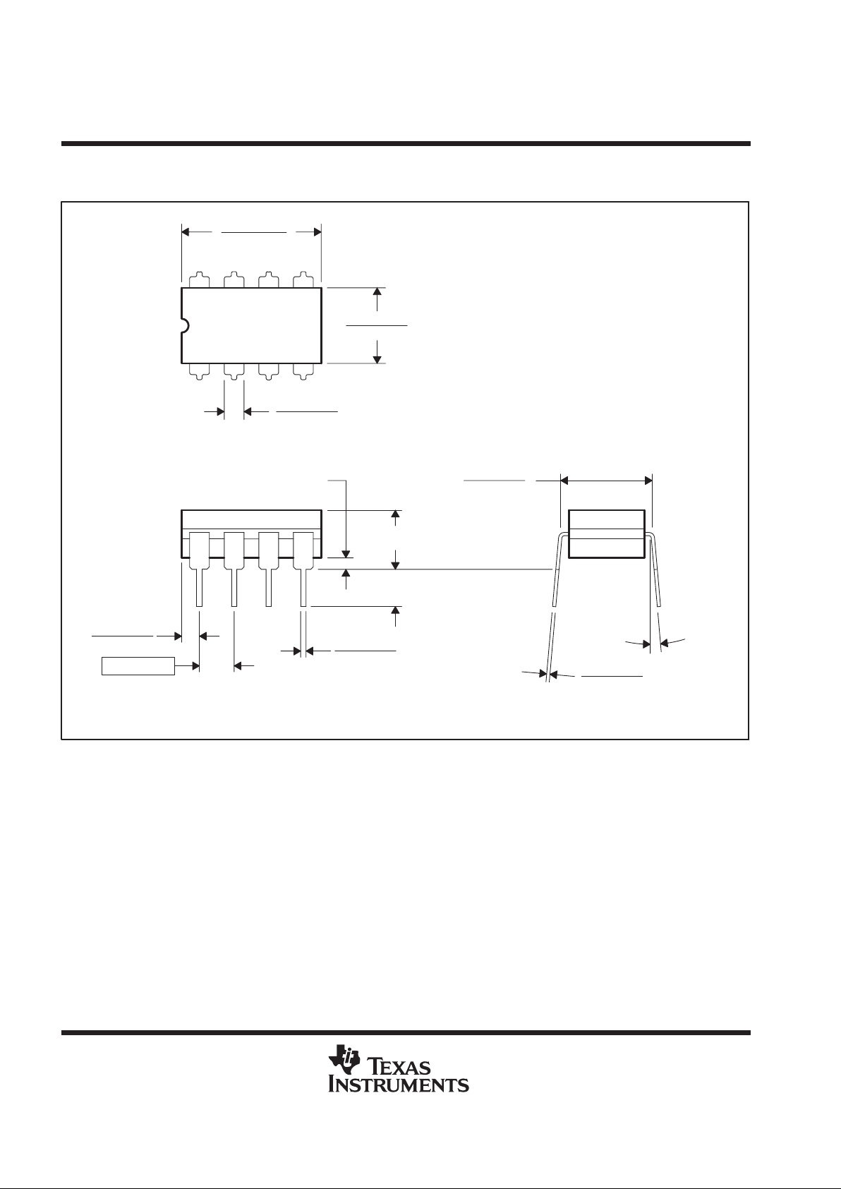
MECHANICAL INFORMATION
D (R-PDSO-G**) PLASTIC SMALL-OUTLINE PACKAGE
14 PIN SHOWN
4040047/D 10/96
0.228 (5,80)
0.244 (6,20)
0.069 (1,75) MAX
0.010 (0,25)
0.004 (0,10)
1
14
0.014 (0,35)
0.020 (0,51)
A
0.157 (4,00)
0.150 (3,81)
7
8
0.044 (1,12)
0.016 (0,40)
Seating Plane
0.010 (0,25)
PINS **
0.008 (0,20) NOM
A MIN
A MAX
DIM
Gage Plane
0.189
(4,80)
(5,00)
0.197
8
(8,55)
(8,75)
0.337
14
0.344
(9,80)
16
0.394
(10,00)
0.386
0.004 (0,10)
M
0.010 (0,25)
0.050 (1,27)
0°–8°
NOTES: A. All linear dimensions are in inches (millimeters).
B. This drawing is subject to change without notice.
C. Body dimensions do not include mold flash or protrusion, not to exceed 0.006 (0,15).
D. Falls within JEDEC MS-012

TLC4501, TLC4501A, TLC4502, TLC4502A
FAMILY OF SELF-CALIBRATING (Self-Cal)
PRECISION CMOS RAIL-TO-RAIL OUTPUT OPERATIONAL AMPLIFIERS
SLOS221A – MA Y 1998 – REVISED JULY 1999
29
POST OFFICE BOX 655303 • DALLAS, TEXAS 75265
MECHANICAL INFORMATION
FK (S-CQCC-N**) LEADLESS CERAMIC CHIP CARRIER
4040140/D 10/96
28 TERMINAL SHOWN
B
0.358
(9,09)
MAX
(11,63)
0.560
(14,22)
0.560
0.458
0.858
(21,8)
1.063
(27,0)
(14,22)
A
NO. OF
MINMAX
0.358
0.660
0.761
0.458
0.342
(8,69)
MIN
(11,23)
(16,26)
0.640
0.739
0.442
(9,09)
(11,63)
(16,76)
0.962
1.165
(23,83)
0.938
(28,99)
1.141
(24,43)
(29,59)
(19,32)(18,78)
**
20
28
52
44
68
84
0.020 (0,51)
TERMINALS
0.080 (2,03)
0.064 (1,63)
(7,80)
0.307
(10,31)
0.406
(12,58)
0.495
(12,58)
0.495
(21,6)
0.850
(26,6)
1.047
0.045 (1,14)
0.045 (1,14)
0.035 (0,89)
0.035 (0,89)
0.010 (0,25)
12
1314151618 17
11
10
8
9
7
5
432
0.020 (0,51)
0.010 (0,25)
6
12826 27
19
21
B SQ
A SQ
22
23
24
25
20
0.055 (1,40)
0.045 (1,14)
0.028 (0,71)
0.022 (0,54)
0.050 (1,27)
NOTES: A. All linear dimensions are in inches (millimeters).
B. This drawing is subject to change without notice.
C. This package can be hermetically sealed with a metal lid.
D. The terminals are gold plated.
E. Falls within JEDEC MS-004
TLC4501, TLC4501A, TLC4502, TLC4502A
FAMILY OF SELF-CALIBRATING (Self-Cal)
PRECISION CMOS RAIL-TO-RAIL OUTPUT OPERATIONAL AMPLIFIERS
SLOS221A – MA Y 1998 – REVISED JULY 1999
30
POST OFFICE BOX 655303 • DALLAS, TEXAS 75265
MECHANICAL INFORMATION
JG (R-GDIP-T8) CERAMIC DUAL-IN-LINE PACKAGE
0.310 (7,87)
0.290 (7,37)
0.014 (0,36)
0.008 (0,20)
Seating Plane
4040107/C 08/96
5
4
0.065 (1,65)
0.045 (1,14)
8
1
0.020 (0,51) MIN
0.400 (10,20)
0.355 (9,00)
0.015 (0,38)
0.023 (0,58)
0.063 (1,60)
0.015 (0,38)
0.200 (5,08) MAX
0.130 (3,30) MIN
0.245 (6,22)
0.280 (7,11)
0.100 (2,54)
0°–15°
NOTES: A. All linear dimensions are in inches (millimeters).
B. This drawing is subject to change without notice.
C. This package can be hermetically sealed with a ceramic lid using glass frit.
D. Index point is provided on cap for terminal identification only on press ceramic glass frit seal only.
E. Falls within MIL-STD-1835 GDIP1-T8

TLC4501, TLC4501A, TLC4502, TLC4502A
FAMILY OF SELF-CALIBRATING (Self-Cal)
PRECISION CMOS RAIL-TO-RAIL OUTPUT OPERATIONAL AMPLIFIERS
SLOS221A – MA Y 1998 – REVISED JULY 1999
31
POST OFFICE BOX 655303 • DALLAS, TEXAS 75265
MECHANICAL INFORMATION
U (S-GDFP-F10) CERAMIC DUAL FLATPACK
4040179/B 03/95
1.000 (25,40)
0.080 (2,03)
0.250 (6,35)
0.250 (6,35)
0.019 (0,48)
0.025 (0,64)
0.300 (7,62)
0.045 (1,14)
0.006 (0,15)
0.050 (1,27)
0.015 (0,38)
0.005 (0,13)
0.026 (0,66)
0.004 (0,10)
0.246 (6,10)
0.750 (19,05)
1
10
5
6
0.250 (6,35)
0.350 (8,89)0.350 (8,89)
0.250 (6,35)
0.050 (1,27)
NOTES: A. All linear dimensions are in inches (millimeters).
B. This drawing is subject to change without notice.
C. This package can be hermetically sealed with a ceramic lid using glass frit.
D. Index point is provided on cap for terminal identification only.
E. Falls within MIL STD 1835 GDFP1-F10 and JEDEC MO-092AA

IMPORTANT NOTICE
T exas Instruments and its subsidiaries (TI) reserve the right to make changes to their products or to discontinue
any product or service without notice, and advise customers to obtain the latest version of relevant information
to verify, before placing orders, that information being relied on is current and complete. All products are sold
subject to the terms and conditions of sale supplied at the time of order acknowledgement, including those
pertaining to warranty, patent infringement, and limitation of liability.
TI warrants performance of its semiconductor products to the specifications applicable at the time of sale in
accordance with TI’s standard warranty. Testing and other quality control techniques are utilized to the extent
TI deems necessary to support this warranty. Specific testing of all parameters of each device is not necessarily
performed, except those mandated by government requirements.
CERT AIN APPLICATIONS USING SEMICONDUCTOR PRODUCTS MAY INVOLVE POTENTIAL RISKS OF
DEATH, PERSONAL INJURY, OR SEVERE PROPERTY OR ENVIRONMENTAL DAMAGE (“CRITICAL
APPLICATIONS”). TI SEMICONDUCTOR PRODUCTS ARE NOT DESIGNED, AUTHORIZED, OR
WARRANTED TO BE SUITABLE FOR USE IN LIFE-SUPPORT DEVICES OR SYSTEMS OR OTHER
CRITICAL APPLICATIONS. INCLUSION OF TI PRODUCTS IN SUCH APPLICA TIONS IS UNDERSTOOD T O
BE FULLY AT THE CUSTOMER’S RISK.
In order to minimize risks associated with the customer’s applications, adequate design and operating
safeguards must be provided by the customer to minimize inherent or procedural hazards.
TI assumes no liability for applications assistance or customer product design. TI does not warrant or represent
that any license, either express or implied, is granted under any patent right, copyright, mask work right, or other
intellectual property right of TI covering or relating to any combination, machine, or process in which such
semiconductor products or services might be or are used. TI’s publication of information regarding any third
party’s products or services does not constitute TI’s approval, warranty or endorsement thereof.
Copyright 1999, Texas Instruments Incorporated
 Loading...