TL16C451, TL16C452
ASYNCHRONOUS COMMUNICATIONS ELEMENTS
SLLS053C – MAY 1989 – REVISED AUGUST 1999
D
Integrates Most Communications Card
Functions From the IBM PC/AT or
Compatibles With Single- or Dual-Channel
Serial Ports
D
TL16C451 Consists of One TL16C450 Plus
Centronix Printer Interface
D
TL16C452 Consists of Two TL16C450s Plus
a Centronix-T ype Printer Interface
description
The TL16C451 and TL16C452 provide single- and dual-channel (respectively) serial interfaces along with a
single Centronix-type parallel-port interface. The serial interfaces provide a serial-to-parallel conversion for data
received from a peripheral device or modem and a parallel-to-serial conversion for data transmitted by a CPU.
The parallel interface provides a bidirectional parallel data port that fully conforms to the requirements for a
Centronix-type printer interface. A CPU can read the status of the asynchronous communications element
(ACE) interfaces at any point in the operation. The status includes the state of the modem signals (CTS
RLSD
, and RI) and any changes to these signals that have occurred since the last time they were read, the state
of the transmitter and receiver including errors detected on received data, and printer status. The TL16C451
and TL16C452 provide control for modem signals (RTS and DTR), interrupt enables, baud rate programming,
and parallel-port control signals.
D
Fully Programmable Serial Interface
Characteristics:
– 5-, 6-, 7-, or 8-Bit Characters
– Even-, Odd-, or No-Parity Bit Generation
and Detection
– 1-, 1 1/2-, or 2 Stop-Bit Generation
– Programmable Baud Rate
(dc to 256 kbit/s)
D
Fully Double Buffered for Reliable
Asynchronous Operation
, DSR,
Please be aware that an important notice concerning availability, standard warranty, and use in critical applications of
Texas Instruments semiconductor products and disclaimers thereto appears at the end of this data sheet.
IBM PC/AT is a trademark of International Business Machines Corporation.
PRODUCTION DATA information is current as of publication date.
Products conform to specifications per the terms of Texas Instruments
standard warranty. Production processing does not necessarily include
testing of all parameters.
POST OFFICE BOX 655303 • DALLAS, TEXAS 75265
Copyright 1999, Texas Instruments Incorporated
1
TL16C451, TL16C452
ASYNCHRONOUS COMMUNICATIONS ELEMENTS
SLLS053C – MAY 1989 – REVISED AUGUST 1999
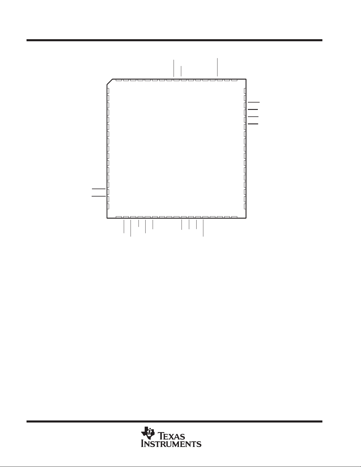
TL16C451 ...FN PACKAGE
(TOP VIEW)
GND
GND
GND
9876543216867666564636261
10
NC
NC
11
NC
12
GND
13
DB0
14
DB1
15
DB2
16
DB3
17
DB4
18
DB5
19
DB6
20
DB7
21
GND
22
V
23
CC
RTS0
DTR0
SOUT0
NC – No internal connection
24
25
26
27 28 29 30 31 32 33 34 35 36 37 38 39 40 41 42 43
GND
CTS0
RLSD0
GND
GNDVGND
CLK
RI0
CS0
DSR0
CC
A2
A1
LPTOE
A0
ACK
IOW
PE
IOR
BUSY
SLCT
CS2
RESET
V
CC
V
CC
GND
ERROR
SIN0
GND
GND
60
59
58
57
56
55
54
53
52
51
50
49
48
47
46
45
44
GND
NC
INT2
SLIN
INIT
AFD
STB
GND
PD0
PD1
PD2
PD3
PD4
PD5
PD6
PD7
INT0
BDO
2
POST OFFICE BOX 655303 • DALLAS, TEXAS 75265
SOUT1
DTR1
RTS1
CTS1
DB0
DB1
DB2
DB3
DB4
DB5
DB6
DB7
GND
V
CC
RTS0
DTR0
SOUT0
ASYNCHRONOUS COMMUNICATIONS ELEMENTS
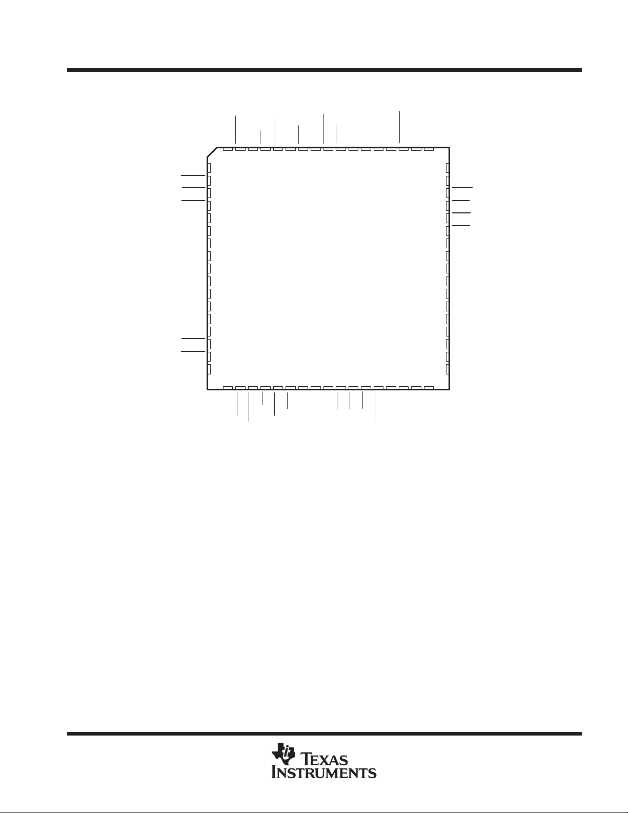
TL16C452 ...FN PACKAGE
(TOP VIEW)
CC
LPTOE
ACK
GND
RLSD1
GND
9876543216867666564636261
10
11
12
13
14
15
16
17
18
19
20
21
22
23
24
25
26
27 28 29 30 31 32 33 34 35 36 37 38 39 40 41 42 43
RI1
CLK
DSR1
CS1
GND
PE
BUSY
SLCT
V
ERROR
TL16C451, TL16C452
SLLS053C – MAY 1989 – REVISED AUGUST 1999
GND
SIN1
60
INT1
59
INT2
58
SLIN
57
INIT
56
AFD
55
STB
54
GND
53
PD0
52
PD1
51
PD2
50
PD3
49
PD4
48
PD5
47
PD6
46
PD7
45
INT0
44
BDO
GND
CTS0
RI0
RLSD0
CS0
DSR0
A2
A1
A0
IOW
IOR
CS2
CC
V
RESET
SIN0
GND
GND
POST OFFICE BOX 655303 • DALLAS, TEXAS 75265
3
TL16C451, TL16C452
ASYNCHRONOUS COMMUNICATIONS ELEMENTS
SLLS053C – MAY 1989 – REVISED AUGUST 1999
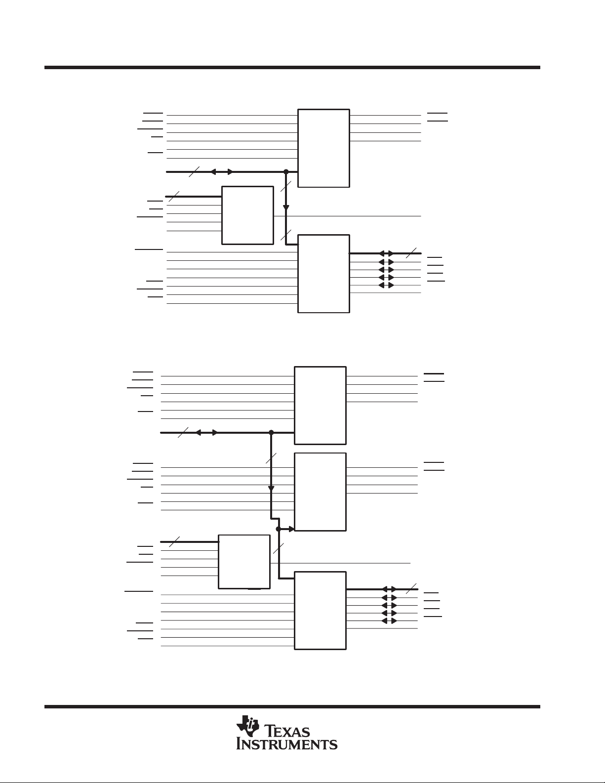
TL16C451 functional block diagram
TL16C451
CTS0
DSR0
RLSD0
RI0
SIN0
CS0
DB0–DB7
A0–A2
IOW
IOR
RESET
CLK
ERROR
SLCT
BUSY
PE
ACK
LPTOE
CS2
8
35 – 33
3
36
37
39
Select
and
Control
4
Logic
28
31
29
30
41
32
14 – 21
8
8
63
65
66
67
68
1
38
ACE
1
Parallel
Port
Parallel
Port
24
25
26
45
53 – 46
57
56
55
58
59
44
8
RTS0
DTR0
SOUT0
INT0
BDO
PD0–PD7
INIT
AFD
STB
SLIN
INT2
TL16C452 functional block diagram
CTS0
DSR0
RLSD0
RI0
SIN0
CS0
DB0–DB7
CTS1
DSR1
RLSD1
RI1
SIN1
CS1
A0–A2
IOW
IOR
RESET
CLK
ERROR
SLCT
BUSY
PE
ACK
LPTOE
CS2
8
3
35 – 33
36
37
39
4
Select
and
Control
Logic
14 – 21
8
28
31
29
30
41
32
13
62
63
65
66
67
68
38
5
8
6
3
8
1
TL16C452
ACE
1
ACE
2
Parallel
Port
24
25
26
45
12
11
10
60
44
53 – 46
57
56
55
58
59
8
RTS0
DTR0
SOUT0
INT0
RTS1
DTR1
SOUT1
INT1
BDO
PD0–PD7
INIT
AFD
STB
SLIN
INT2
4
POST OFFICE BOX 655303 • DALLAS, TEXAS 75265
TL16C451, TL16C452
I/O
DESCRIPTION
ASYNCHRONOUS COMMUNICATIONS ELEMENTS
SLLS053C – MAY 1989 – REVISED AUGUST 1999
Terminal Functions
TERMINAL
†
NAME
A0
A1
A2
ACK
AFD
BDO 44 O Bus buffer output. BDO is active (high) when the CPU is reading data. When active, this output can
BUSY 66 I Printer busy. BUSY is an input line from the printer that goes high when the printer is not ready to accept
CLK 4 I/O External clock. CLK connects the ACE to the main timing reference.
CS0
CS1 [VCC]
CS2
CTS0
CTS1 [GND]
DB0 – DB7 14 – 21
DSR0
DSR1 [GND]
DTR0
DTR1 [NC]
ERROR 63 I
INIT 57
INT0
INT1 [NC]
INT2 59 O
IOR
IOW
LPTOE
†
Names shown in brackets are for the TL16C451.
NO.
35
34
33
68 I
56 I/O
32
3
38
28
13
31
5
25
11
45
60
37 I
36 I
1 I
Register select. A0, A1, and A2 are used during read and write operations to select the register to read
I
from or write to. Refer to T able 1 for register addresses, also refer to the chip select signals (CS0
).
CS2
Printer acknowledge. ACK goes low to indicate that a successful data transfer has taken place. It
generates a printer port interrupt during its positive transition.
Printer autofeed. AFD is an open-drain line that provides the printer with a low signal when
continuous-form paper is to be autofed to the printer. An internal pullup is provided.
disable an external transceiver.
data.
Chip selects. Each chip select enables read and write operations to its respective channel. CS0 and
I
I
I/O Data bus. Eight 3-state data lines provide a bidirectional path for data, control, and status information
I
O
I/O
O Interrupt. INTx is an active-high 3-state output that is enabled by bit 3 of the MCR. When active, INTx
select serial channels 0 and 1, respectively, and CS2 selects the parallel port.
CS1
Clear to send. CTSx is an active-low modem status signal. Its state can be checked by reading bit 4
(CTS) of the modem status register. Bit 0 (DCTS) of the modem status register indicates that this signal
has changed states since the last read from the modem status register. If the modem status interrupt
is enabled when CTSx
between the TL16C451/TL16C452 and the CPU. DB0 is the least significant bit (LSB).
Data set ready. DSRx is an active-low modem status signal. Its state can be checked by reading
bit 5 (DSR) of the modem status register. Bit 1 (DDSR) of the modem status register indicates that this
signal has changed states since the last read from the modem status register. If the modem status
interrupt is enabled when the DSRx
Data terminal ready. DTRx, when active (low), informs a modem or data set that the ACE is ready to
establish communication. DTRx
register. DTRx
or clearing bit 0 (DTR) of the modem control register.
Printer error. ERROR is an input line from the printer. The printer reports an error by holding this line
low during the error condition.
Printer initialize. INIT is an open-drain line that provides the printer with a signal that allows the printer
initialization routine to be started. An internal pullup is provided.
informs the CPU that the ACE has an interrupt to be serviced. Four conditions that cause an interrupt
to be issued are: a receiver error, received data is available, the transmitter holding register is empty,
and an enabled modem status interrupt. The INTx output is reset (low) either when the interrupt is
serviced or as a result of a reset.
Printer port interrupt. INT2 is an active-high 3-state output generated by the positive transition of ACK.
It is enabled by bit 4 of the write control register.
Data read strobe. When IOR input is active (low) while the ACE is selected, the CPU is allowed to read
status information or data from a selected ACE register.
Data write strobe. When IOW input is active (low) while the ACE is selected, the CPU is allowed to write
control words or data into a selected ACE register.
Parallel data output enable. When low, LPT OE enables the write data register to the PD0–PD7 lines.
A high puts the PD0–PD7 lines in the high-impedance state allowing them to be used as inputs. LPTOE
is usually tied low for printer operation.
changes state, an interrupt is generated.
changes state, an interrupt is generated.
is placed in the active state by setting the DTR bit of the modem control
is placed in the inactive state either as a result of a reset or during loop mode operation
, CS1,
POST OFFICE BOX 655303 • DALLAS, TEXAS 75265
5
TL16C451, TL16C452
I/O
DESCRIPTION
ASYNCHRONOUS COMMUNICATIONS ELEMENTS
SLLS053C – MAY 1989 – REVISED AUGUST 1999
Terminal Functions (continued)
TERMINAL
†
NAME
PD0–PD7 53–46 I/O Parallel data bits (0–7). These eight lines provide a byte-wide input or output port to the system. The
PE 67 I Printer paper empty. This is an input line from the printer that goes high when the printer runs out of
RESET
RI0
RI1 [GND]
RLSD0
RLSD1 [GND]
RTS0
RTS1 [NC]
SIN0
SIN1 [GND]
SLCT 65 I Printer selected. SLCT is an input line from the printer that goes high when the printer has been selected.
SLIN
SOUT0
SOUT1 [NC]
STB
V
CC
GND 2,7,9
†
Names shown in brackets are for the TL16C451.
NO.
39 I
30
6
29
8
24
12
41
62
58 I/O
26
10
55 I/O
23,40,
64
22,27,42,
43,54,61
eight lines are held in a high-impedance state when LPTOE
paper.
Reset. When active (low), RESET clears most ACE registers and sets the state of various output
signals. Refer to Table 2.
I
Ring indicator. RIx is an active-low modem status signal. Its state can be checked by reading bit 6 (RI)
of the modem status register. Bit 2 (TERI) of the modem status register indicates that the RIx
transitioned from a low to a high state since the last read from the modem status register. If the modem
status interrupt is enabled when this transition occurs, an interrupt is generated.
I
Receive line signal detect. RLSDx is an active-low modem status signal. Its state can be checked by
reading bit 7 of the modem status register. Bit 3 (DRLSD) of the modem status register indicates that
this signal has changed states since the last read from the modem status register. If the modem status
interrupt is enabled when RLSDx
carrier is detected.
O
Request to send. When active (low), RTSx informs the modem or data set that the ACE is ready to
transmit data. RTSx
to its inactive (high) state either as a result of a reset or during loop mode operations or by clearing bit
1 (RTS) of the modem control register.
I Serial input. SINx is a serial data input from a connected communications device.
Printer select. SLIN is an open-drain line that selects the printer when it is active (low). An internal pullup
is provided on this line.
I Serial output. SOUTx is a composite serial data output to a connected communication device. SOUTx
is set during a reset.
Printer strobe. STB is an open-drain line that provides communication synchronization between the
TL16C451/TL16C452 and the printer . When it is active (low), it provides the printer with a signal to latch
the data currently on the parallel port. An internal pullup is provided on this line.
5-V supply voltage
Supply common
is set to its active state by setting the RTS modem control register bit and is set
changes state, an interrupt is generated. This bit is low when a data
is high.
input has
6
POST OFFICE BOX 655303 • DALLAS, TEXAS 75265
TL16C451, TL16C452
VOHHigh-level output voltage
2.4
V
I
Input leakage current
CC
,
SS
,
±10µA
All other in uts at 0.8 V,XTAL1 at 4 MHz
ASYNCHRONOUS COMMUNICATIONS ELEMENTS
SLLS053C – MAY 1989 – REVISED AUGUST 1999
absolute maximum ratings over operating free-air temperature range (unless otherwise noted)
†
Supply voltage range, VCC (see Note 1 ) –0.5 V to 7 V. . . . . . . . . . . . . . . . . . . . . . . . . . . . . . . . . . . . . . . . . . . . . .
Input voltage range at any input, VI –0.5 V to 7 V. . . . . . . . . . . . . . . . . . . . . . . . . . . . . . . . . . . . . . . . . . . . . . . . . . .
Output voltage range, VO –0.5 V to 7 V. . . . . . . . . . . . . . . . . . . . . . . . . . . . . . . . . . . . . . . . . . . . . . . . . . . . . . . . . . .
Continuous total power dissipation 1100 mW. . . . . . . . . . . . . . . . . . . . . . . . . . . . . . . . . . . . . . . . . . . . . . . . . . . . . . .
Operating free-air temperature range, T
Storage temperature range, T
–65°C to 150°C. . . . . . . . . . . . . . . . . . . . . . . . . . . . . . . . . . . . . . . . . . . . . . . . . .
stg
0°C to 70°C. . . . . . . . . . . . . . . . . . . . . . . . . . . . . . . . . . . . . . . . . . . . .
A
Case temperature for 10 seconds, TC 260°C. . . . . . . . . . . . . . . . . . . . . . . . . . . . . . . . . . . . . . . . . . . . . . . . . . . . . .
†
Stresses beyond those listed under “absolute maximum ratings” may cause permanent damage to the device. These are stress ratings only and
functional operation of the device at these or any other conditions beyond those indicated under “recommended operating conditions” is not
implied. Exposure to absolute-maximum-rated conditions for extended periods may affect device reliability.
NOTE 1: All voltage values are with respect to GND.
recommended operating conditions
MIN NOM MAX UNIT
Supply voltage, V
High-level Input voltage, V
Low-level Input voltage, V
Operating free-air temperature, T
CC
IH
IL
A
4.75 5 5.25 V
2 V
–0.5 0.8 V
0 70 °C
CC
V
electrical characteristics over recommended ranges of supply voltage and operating free-air
temperature (unless otherwise noted)
PARAMETER TEST CONDITIONS MIN TYP†MAX UNIT
IOH = –0.4 mA on DB0–DB7
p
V
OL
Ikg
I
oz
I
CC
†
All typical values are at VCC = 5 V, TA = 25°C.
NOTE 2: INIT
Low-level output voltage
p
High-impedance output current
Supply current
, AFD, STB, and SLIN are open-collector output terminals that each have an internal pullup to VCC. This generates a maximum of
2 mA of internal IOL per terminal. In addition to this internal current, each terminal sinks at least 10 mA while maintaining the V
specification of 0.4 V maximum.
IOH = –2 mA to 4 mA on PD0–PD7
IOH = –0.2 mA on INIT, AFD, STB, and SLIN
IOH = –0.2 mA on all other outputs
IOL = 4 mA on DB0–DB7
IOL = 12 mA on PD0–PD7
IOL = 10 mA on INIT,
AFD, STB, and SLIN (see Note 2)
IOL = 2 mA on all other outputs
V
= 5.25 V, V
VI = 0 to 5.25 V, All other terminals floating
VCC = 5.25 V, VSS = 0,
VO = 0 to 5.25 V,
Chip selected and in write mode, or chip deselected
VCC = 5.25 V, VSS = 0,
SIN, DSR, RLSD, CTS, and RI at 2 V,
p
No load on outputs, Baud rate = 50 kbit/s
= 0,
,
0.4 V
±20 µA
10 mA
OL
system timing requirements over recommended ranges of supply voltage and operating free-air
temperature
t
cR
Cycle time, read (tw7 + td8 + td9) 175 ns
PARAMETER FIGURE MIN MAX UNIT
POST OFFICE BOX 655303 • DALLAS, TEXAS 75265
7
 Loading...