


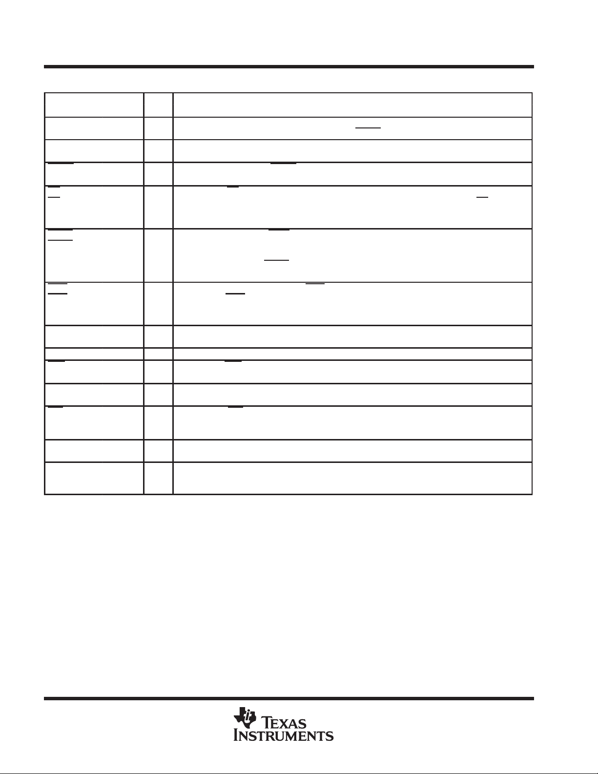
TL16C451, TL16C452
ASYNCHRONOUS COMMUNICATIONS ELEMENTS
SLLS053C – MAY 1989 – REVISED AUGUST 1999
D
Integrates Most Communications Card
Functions From the IBM PC/AT or
Compatibles With Single- or Dual-Channel
Serial Ports
D
TL16C451 Consists of One TL16C450 Plus
Centronix Printer Interface
D
TL16C452 Consists of Two TL16C450s Plus
a Centronix-T ype Printer Interface
description
The TL16C451 and TL16C452 provide single- and dual-channel (respectively) serial interfaces along with a
single Centronix-type parallel-port interface. The serial interfaces provide a serial-to-parallel conversion for data
received from a peripheral device or modem and a parallel-to-serial conversion for data transmitted by a CPU.
The parallel interface provides a bidirectional parallel data port that fully conforms to the requirements for a
Centronix-type printer interface. A CPU can read the status of the asynchronous communications element
(ACE) interfaces at any point in the operation. The status includes the state of the modem signals (CTS
RLSD
, and RI) and any changes to these signals that have occurred since the last time they were read, the state
of the transmitter and receiver including errors detected on received data, and printer status. The TL16C451
and TL16C452 provide control for modem signals (RTS and DTR), interrupt enables, baud rate programming,
and parallel-port control signals.
D
Fully Programmable Serial Interface
Characteristics:
– 5-, 6-, 7-, or 8-Bit Characters
– Even-, Odd-, or No-Parity Bit Generation
and Detection
– 1-, 1 1/2-, or 2 Stop-Bit Generation
– Programmable Baud Rate
(dc to 256 kbit/s)
D
Fully Double Buffered for Reliable
Asynchronous Operation
, DSR,
Please be aware that an important notice concerning availability, standard warranty, and use in critical applications of
Texas Instruments semiconductor products and disclaimers thereto appears at the end of this data sheet.
IBM PC/AT is a trademark of International Business Machines Corporation.
PRODUCTION DATA information is current as of publication date.
Products conform to specifications per the terms of Texas Instruments
standard warranty. Production processing does not necessarily include
testing of all parameters.
POST OFFICE BOX 655303 • DALLAS, TEXAS 75265
Copyright 1999, Texas Instruments Incorporated
1
TL16C451, TL16C452
ASYNCHRONOUS COMMUNICATIONS ELEMENTS
SLLS053C – MAY 1989 – REVISED AUGUST 1999
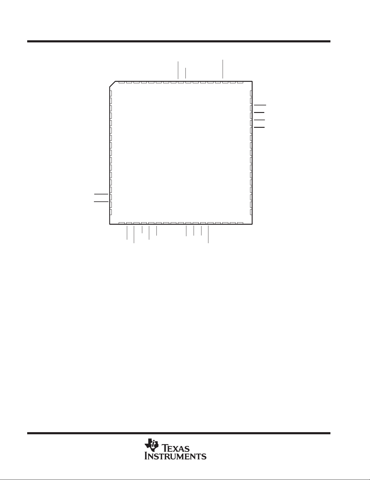
TL16C451 ...FN PACKAGE
(TOP VIEW)
GND
GND
GND
9876543216867666564636261
10
NC
NC
11
NC
12
GND
13
DB0
14
DB1
15
DB2
16
DB3
17
DB4
18
DB5
19
DB6
20
DB7
21
GND
22
V
23
CC
RTS0
DTR0
SOUT0
NC – No internal connection
24
25
26
27 28 29 30 31 32 33 34 35 36 37 38 39 40 41 42 43
GND
CTS0
RLSD0
GND
GNDVGND
CLK
RI0
CS0
DSR0
CC
A2
A1
LPTOE
A0
ACK
IOW
PE
IOR
BUSY
SLCT
CS2
RESET
V
CC
V
CC
GND
ERROR
SIN0
GND
GND
60
59
58
57
56
55
54
53
52
51
50
49
48
47
46
45
44
GND
NC
INT2
SLIN
INIT
AFD
STB
GND
PD0
PD1
PD2
PD3
PD4
PD5
PD6
PD7
INT0
BDO
2
POST OFFICE BOX 655303 • DALLAS, TEXAS 75265
SOUT1
DTR1
RTS1
CTS1
DB0
DB1
DB2
DB3
DB4
DB5
DB6
DB7
GND
V
CC
RTS0
DTR0
SOUT0
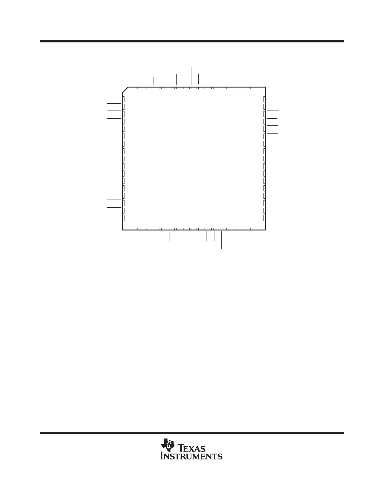
ASYNCHRONOUS COMMUNICATIONS ELEMENTS
TL16C452 ...FN PACKAGE
(TOP VIEW)
CC
LPTOE
ACK
GND
RLSD1
GND
9876543216867666564636261
10
11
12
13
14
15
16
17
18
19
20
21
22
23
24
25
26
27 28 29 30 31 32 33 34 35 36 37 38 39 40 41 42 43
RI1
CLK
DSR1
CS1
GND
PE
BUSY
SLCT
V
ERROR
TL16C451, TL16C452
SLLS053C – MAY 1989 – REVISED AUGUST 1999
GND
SIN1
60
INT1
59
INT2
58
SLIN
57
INIT
56
AFD
55
STB
54
GND
53
PD0
52
PD1
51
PD2
50
PD3
49
PD4
48
PD5
47
PD6
46
PD7
45
INT0
44
BDO
GND
CTS0
RI0
RLSD0
CS0
DSR0
A2
A1
A0
IOW
IOR
CS2
CC
V
RESET
SIN0
GND
GND
POST OFFICE BOX 655303 • DALLAS, TEXAS 75265
3
TL16C451, TL16C452
ASYNCHRONOUS COMMUNICATIONS ELEMENTS
SLLS053C – MAY 1989 – REVISED AUGUST 1999
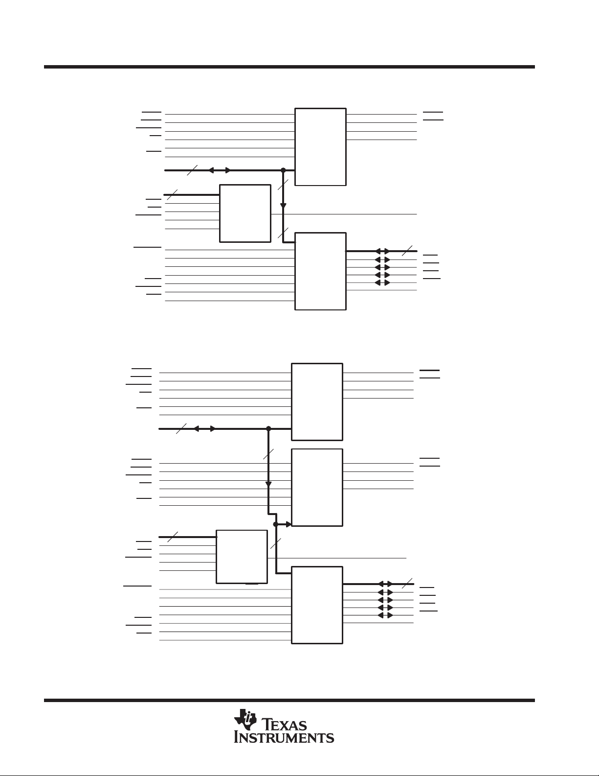
TL16C451 functional block diagram
TL16C451
CTS0
DSR0
RLSD0
RI0
SIN0
CS0
DB0–DB7
A0–A2
IOW
IOR
RESET
CLK
ERROR
SLCT
BUSY
PE
ACK
LPTOE
CS2
8
35 – 33
3
36
37
39
Select
and
Control
4
Logic
28
31
29
30
41
32
14 – 21
8
8
63
65
66
67
68
1
38
ACE
1
Parallel
Port
Parallel
Port
24
25
26
45
53 – 46
57
56
55
58
59
44
8
RTS0
DTR0
SOUT0
INT0
BDO
PD0–PD7
INIT
AFD
STB
SLIN
INT2
TL16C452 functional block diagram
CTS0
DSR0
RLSD0
RI0
SIN0
CS0
DB0–DB7
CTS1
DSR1
RLSD1
RI1
SIN1
CS1
A0–A2
IOW
IOR
RESET
CLK
ERROR
SLCT
BUSY
PE
ACK
LPTOE
CS2
8
3
35 – 33
36
37
39
4
Select
and
Control
Logic
14 – 21
8
28
31
29
30
41
32
13
62
63
65
66
67
68
38
5
8
6
3
8
1
TL16C452
ACE
1
ACE
2
Parallel
Port
24
25
26
45
12
11
10
60
44
53 – 46
57
56
55
58
59
8
RTS0
DTR0
SOUT0
INT0
RTS1
DTR1
SOUT1
INT1
BDO
PD0–PD7
INIT
AFD
STB
SLIN
INT2
4
POST OFFICE BOX 655303 • DALLAS, TEXAS 75265
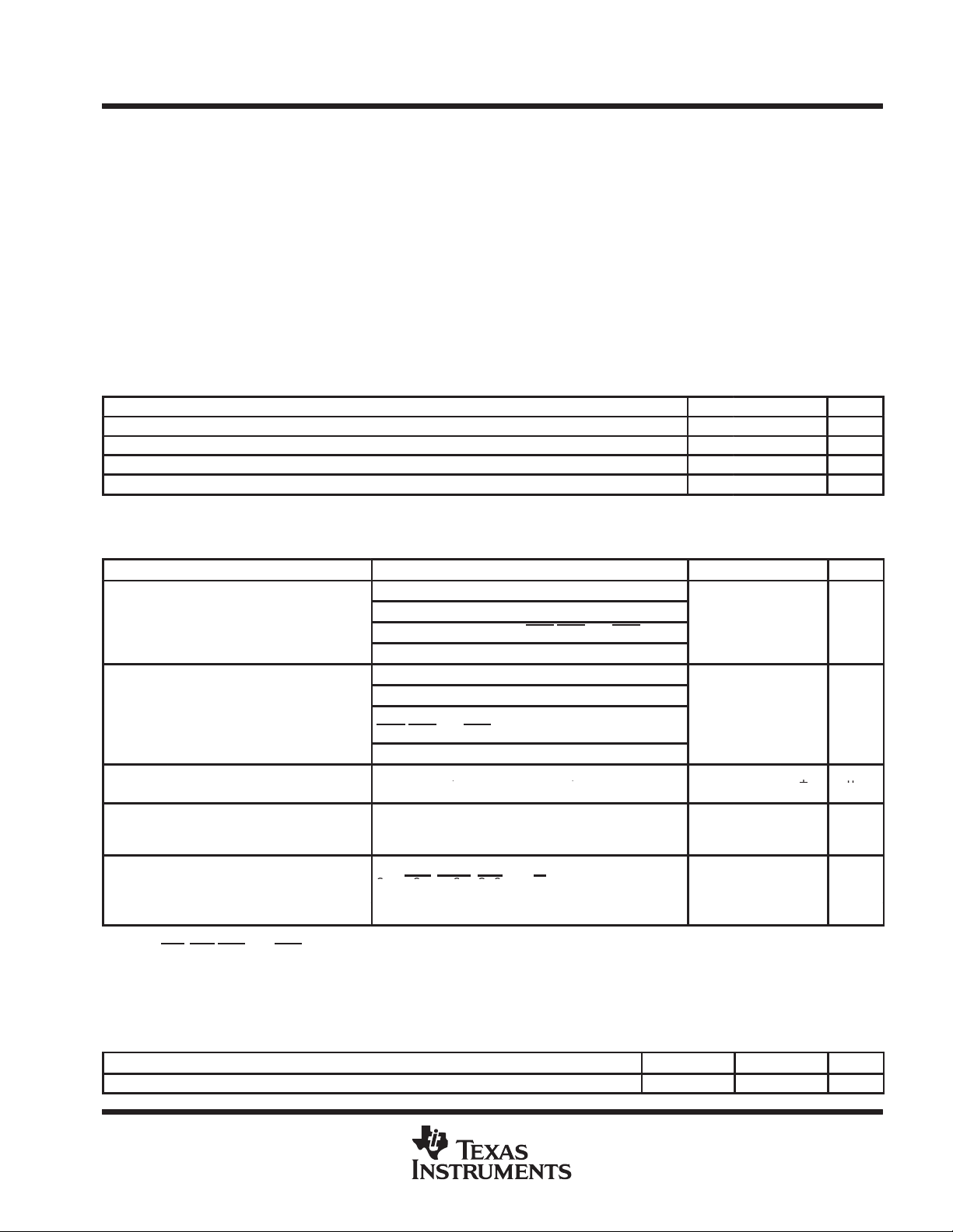
TL16C451, TL16C452
I/O
DESCRIPTION
ASYNCHRONOUS COMMUNICATIONS ELEMENTS
SLLS053C – MAY 1989 – REVISED AUGUST 1999
Terminal Functions
TERMINAL
†
NAME
A0
A1
A2
ACK
AFD
BDO 44 O Bus buffer output. BDO is active (high) when the CPU is reading data. When active, this output can
BUSY 66 I Printer busy. BUSY is an input line from the printer that goes high when the printer is not ready to accept
CLK 4 I/O External clock. CLK connects the ACE to the main timing reference.
CS0
CS1 [VCC]
CS2
CTS0
CTS1 [GND]
DB0 – DB7 14 – 21
DSR0
DSR1 [GND]
DTR0
DTR1 [NC]
ERROR 63 I
INIT 57
INT0
INT1 [NC]
INT2 59 O
IOR
IOW
LPTOE
†
Names shown in brackets are for the TL16C451.
NO.
35
34
33
68 I
56 I/O
32
3
38
28
13
31
5
25
11
45
60
37 I
36 I
1 I
Register select. A0, A1, and A2 are used during read and write operations to select the register to read
I
from or write to. Refer to T able 1 for register addresses, also refer to the chip select signals (CS0
).
CS2
Printer acknowledge. ACK goes low to indicate that a successful data transfer has taken place. It
generates a printer port interrupt during its positive transition.
Printer autofeed. AFD is an open-drain line that provides the printer with a low signal when
continuous-form paper is to be autofed to the printer. An internal pullup is provided.
disable an external transceiver.
data.
Chip selects. Each chip select enables read and write operations to its respective channel. CS0 and
I
I
I/O Data bus. Eight 3-state data lines provide a bidirectional path for data, control, and status information
I
O
I/O
O Interrupt. INTx is an active-high 3-state output that is enabled by bit 3 of the MCR. When active, INTx
select serial channels 0 and 1, respectively, and CS2 selects the parallel port.
CS1
Clear to send. CTSx is an active-low modem status signal. Its state can be checked by reading bit 4
(CTS) of the modem status register. Bit 0 (DCTS) of the modem status register indicates that this signal
has changed states since the last read from the modem status register. If the modem status interrupt
is enabled when CTSx
between the TL16C451/TL16C452 and the CPU. DB0 is the least significant bit (LSB).
Data set ready. DSRx is an active-low modem status signal. Its state can be checked by reading
bit 5 (DSR) of the modem status register. Bit 1 (DDSR) of the modem status register indicates that this
signal has changed states since the last read from the modem status register. If the modem status
interrupt is enabled when the DSRx
Data terminal ready. DTRx, when active (low), informs a modem or data set that the ACE is ready to
establish communication. DTRx
register. DTRx
or clearing bit 0 (DTR) of the modem control register.
Printer error. ERROR is an input line from the printer. The printer reports an error by holding this line
low during the error condition.
Printer initialize. INIT is an open-drain line that provides the printer with a signal that allows the printer
initialization routine to be started. An internal pullup is provided.
informs the CPU that the ACE has an interrupt to be serviced. Four conditions that cause an interrupt
to be issued are: a receiver error, received data is available, the transmitter holding register is empty,
and an enabled modem status interrupt. The INTx output is reset (low) either when the interrupt is
serviced or as a result of a reset.
Printer port interrupt. INT2 is an active-high 3-state output generated by the positive transition of ACK.
It is enabled by bit 4 of the write control register.
Data read strobe. When IOR input is active (low) while the ACE is selected, the CPU is allowed to read
status information or data from a selected ACE register.
Data write strobe. When IOW input is active (low) while the ACE is selected, the CPU is allowed to write
control words or data into a selected ACE register.
Parallel data output enable. When low, LPT OE enables the write data register to the PD0–PD7 lines.
A high puts the PD0–PD7 lines in the high-impedance state allowing them to be used as inputs. LPTOE
is usually tied low for printer operation.
changes state, an interrupt is generated.
changes state, an interrupt is generated.
is placed in the active state by setting the DTR bit of the modem control
is placed in the inactive state either as a result of a reset or during loop mode operation
, CS1,
POST OFFICE BOX 655303 • DALLAS, TEXAS 75265
5
TL16C451, TL16C452
I/O
DESCRIPTION
ASYNCHRONOUS COMMUNICATIONS ELEMENTS
SLLS053C – MAY 1989 – REVISED AUGUST 1999
Terminal Functions (continued)
TERMINAL
†
NAME
PD0–PD7 53–46 I/O Parallel data bits (0–7). These eight lines provide a byte-wide input or output port to the system. The
PE 67 I Printer paper empty. This is an input line from the printer that goes high when the printer runs out of
RESET
RI0
RI1 [GND]
RLSD0
RLSD1 [GND]
RTS0
RTS1 [NC]
SIN0
SIN1 [GND]
SLCT 65 I Printer selected. SLCT is an input line from the printer that goes high when the printer has been selected.
SLIN
SOUT0
SOUT1 [NC]
STB
V
CC
GND 2,7,9
†
Names shown in brackets are for the TL16C451.
NO.
39 I
30
6
29
8
24
12
41
62
58 I/O
26
10
55 I/O
23,40,
64
22,27,42,
43,54,61
eight lines are held in a high-impedance state when LPTOE
paper.
Reset. When active (low), RESET clears most ACE registers and sets the state of various output
signals. Refer to Table 2.
I
Ring indicator. RIx is an active-low modem status signal. Its state can be checked by reading bit 6 (RI)
of the modem status register. Bit 2 (TERI) of the modem status register indicates that the RIx
transitioned from a low to a high state since the last read from the modem status register. If the modem
status interrupt is enabled when this transition occurs, an interrupt is generated.
I
Receive line signal detect. RLSDx is an active-low modem status signal. Its state can be checked by
reading bit 7 of the modem status register. Bit 3 (DRLSD) of the modem status register indicates that
this signal has changed states since the last read from the modem status register. If the modem status
interrupt is enabled when RLSDx
carrier is detected.
O
Request to send. When active (low), RTSx informs the modem or data set that the ACE is ready to
transmit data. RTSx
to its inactive (high) state either as a result of a reset or during loop mode operations or by clearing bit
1 (RTS) of the modem control register.
I Serial input. SINx is a serial data input from a connected communications device.
Printer select. SLIN is an open-drain line that selects the printer when it is active (low). An internal pullup
is provided on this line.
I Serial output. SOUTx is a composite serial data output to a connected communication device. SOUTx
is set during a reset.
Printer strobe. STB is an open-drain line that provides communication synchronization between the
TL16C451/TL16C452 and the printer . When it is active (low), it provides the printer with a signal to latch
the data currently on the parallel port. An internal pullup is provided on this line.
5-V supply voltage
Supply common
is set to its active state by setting the RTS modem control register bit and is set
changes state, an interrupt is generated. This bit is low when a data
is high.
input has
6
POST OFFICE BOX 655303 • DALLAS, TEXAS 75265
TL16C451, TL16C452
VOHHigh-level output voltage
2.4
V
I
Input leakage current
CC
,
SS
,
±10µA
All other in uts at 0.8 V,XTAL1 at 4 MHz
ASYNCHRONOUS COMMUNICATIONS ELEMENTS
SLLS053C – MAY 1989 – REVISED AUGUST 1999
absolute maximum ratings over operating free-air temperature range (unless otherwise noted)
†
Supply voltage range, VCC (see Note 1 ) –0.5 V to 7 V. . . . . . . . . . . . . . . . . . . . . . . . . . . . . . . . . . . . . . . . . . . . . .
Input voltage range at any input, VI –0.5 V to 7 V. . . . . . . . . . . . . . . . . . . . . . . . . . . . . . . . . . . . . . . . . . . . . . . . . . .
Output voltage range, VO –0.5 V to 7 V. . . . . . . . . . . . . . . . . . . . . . . . . . . . . . . . . . . . . . . . . . . . . . . . . . . . . . . . . . .
Continuous total power dissipation 1100 mW. . . . . . . . . . . . . . . . . . . . . . . . . . . . . . . . . . . . . . . . . . . . . . . . . . . . . . .
Operating free-air temperature range, T
Storage temperature range, T
–65°C to 150°C. . . . . . . . . . . . . . . . . . . . . . . . . . . . . . . . . . . . . . . . . . . . . . . . . .
stg
0°C to 70°C. . . . . . . . . . . . . . . . . . . . . . . . . . . . . . . . . . . . . . . . . . . . .
A
Case temperature for 10 seconds, TC 260°C. . . . . . . . . . . . . . . . . . . . . . . . . . . . . . . . . . . . . . . . . . . . . . . . . . . . . .
†
Stresses beyond those listed under “absolute maximum ratings” may cause permanent damage to the device. These are stress ratings only and
functional operation of the device at these or any other conditions beyond those indicated under “recommended operating conditions” is not
implied. Exposure to absolute-maximum-rated conditions for extended periods may affect device reliability.
NOTE 1: All voltage values are with respect to GND.
recommended operating conditions
MIN NOM MAX UNIT
Supply voltage, V
High-level Input voltage, V
Low-level Input voltage, V
Operating free-air temperature, T
CC
IH
IL
A
4.75 5 5.25 V
2 V
–0.5 0.8 V
0 70 °C
CC
V
electrical characteristics over recommended ranges of supply voltage and operating free-air
temperature (unless otherwise noted)
PARAMETER TEST CONDITIONS MIN TYP†MAX UNIT
IOH = –0.4 mA on DB0–DB7
p
V
OL
Ikg
I
oz
I
CC
†
All typical values are at VCC = 5 V, TA = 25°C.
NOTE 2: INIT
Low-level output voltage
p
High-impedance output current
Supply current
, AFD, STB, and SLIN are open-collector output terminals that each have an internal pullup to VCC. This generates a maximum of
2 mA of internal IOL per terminal. In addition to this internal current, each terminal sinks at least 10 mA while maintaining the V
specification of 0.4 V maximum.
IOH = –2 mA to 4 mA on PD0–PD7
IOH = –0.2 mA on INIT, AFD, STB, and SLIN
IOH = –0.2 mA on all other outputs
IOL = 4 mA on DB0–DB7
IOL = 12 mA on PD0–PD7
IOL = 10 mA on INIT,
AFD, STB, and SLIN (see Note 2)
IOL = 2 mA on all other outputs
V
= 5.25 V, V
VI = 0 to 5.25 V, All other terminals floating
VCC = 5.25 V, VSS = 0,
VO = 0 to 5.25 V,
Chip selected and in write mode, or chip deselected
VCC = 5.25 V, VSS = 0,
SIN, DSR, RLSD, CTS, and RI at 2 V,
p
No load on outputs, Baud rate = 50 kbit/s
= 0,
,
0.4 V
±20 µA
10 mA
OL
system timing requirements over recommended ranges of supply voltage and operating free-air
temperature
t
cR
Cycle time, read (tw7 + td8 + td9) 175 ns
PARAMETER FIGURE MIN MAX UNIT
POST OFFICE BOX 655303 • DALLAS, TEXAS 75265
7

TL16C451, TL16C452
t
Del
k)↑ t
(INTRPT)↑
411
t
Del
itial
THR (IOW)↑ to t
(SOUT)↓
5824
t
Del
(SOUT) l
(INTRPT)↑
588
t
Del
itial
(IOW)↑ to THRE int
(INTRPT)↑
51632
ASYNCHRONOUS COMMUNICATIONS ELEMENTS
SLLS053C – MAY 1989 – REVISED AUGUST 1999
t
cW
t
w1
t
w2
t
w5
t
w6
t
wRST
t
su1
t
su2
t
su3
t
h1
t
h2
t
h3
t
d3
t
d4
Cycle time, write (tw6 + td5 + td6) 175 ns
Pulse duration, clock↑ 1 50 ns
Pulse duration, clock↓ 1 50 ns
Pulse duration, write strobe (IOW)↑ 2 80 ns
Pulse duration, read strobe (IOR)↓ 3 80 ns
Pulse duration, reset 1000 ns
Setup time, address (A0 – A2) valid before IOW↓ 2,3 15 ns
Setup time, chip select (CSx) valid before IOW↓ 2,3 15 ns
Setup time, data (D0 – D7) valid before IOW↑ 2 15 ns
Hold time, address (A0 – A2) valid after IOW↑ 2,3 20 ns
Hold time, chip select (CSx) valid after IOW↑ 2,3 20 ns
Hold time, data (D0 – D7) valid before IOW↑ 2 15 ns
Delay time, write cycle (IOW)↑ to IOW↓ 2 80 ns
Delay time, read cycle (IOR)↑ to IOR↓ 3 80 ns
system switching characteristics over recommended ranges of supply voltage and operating
free-air temperature
PARAMETER FIGURE TEST CONDITIONS MIN MAX UNIT
t
d5
t
d6
t
dis(R)
Delay time, data (D0 – D7) valid before read (IOR)↑ 3 CL = 100 pF 60 ns
Delay time, floating data (D0 – D7) valid after read (IOR)↑ 3 CL = 100 pF 0 60 ns
Read to driver disable, IOR↓ to BD0↓ 3 CL = 100 pF 60 ns
receiver switching characteristics over recommended ranges of supply voltage and operating
free-air temperature
PARAMETER FIGURE TEST CONDITIONS MIN MAX UNIT
t
Delay time, RCLK↑ to sample clock↑ 4 100 ns
d7
d8
t
d9
ay time, stop (sample cloc
Delay time, read RBR/LSR (IOR)↑ to reset interrupt (INTRPT)↓ 4 CL = 100 pF 140 ns
o set interrupt
RCLK
cycles
transmitter switching characteristics over recommended ranges of supply voltage and operating
free-air temperature
PARAMETER FIGURE TEST CONDITIONS MIN MAX UNIT
d10
d11
t
d12
d13
t
d14
ay time, in
ay time, stop
Delay time, write THR (IOW)↓ to reset interrupt (INTRPT) low 5 CL = 100 pF 140 ns
ay time, in
Delay time, read IIR (IOR)↑ to reset THRE interrupt (INTRPT) low 5 CL = 100 pF 140 ns
write
write
ransmit start
ow to interrupt
errupt
baudout
cycles
baudout
cycles
baudout
cycles
modem control switching characteristics over recommended ranges of supply voltage and
operating free-air temperature
PARAMETER FIGURE TEST CONDITIONS MIN MAX UNIT
t
Delay time, write MCR (IOW)↑ to output (RTS, DTS)↓↑ 6 CL = 100 pF 100 ns
d15
8
POST OFFICE BOX 655303 • DALLAS, TEXAS 75265

TL16C451, TL16C452
ASYNCHRONOUS COMMUNICATIONS ELEMENTS
SLLS053C – MAY 1989 – REVISED AUGUST 1999
Delay time, modem input (CTS, DSR, RLSD)↑ to set interrupt
t
d16
(INTRPT) high
t
Delay time, read MSR (IOR)↑ to reset interrupt (INTRPT) low 6 CL = 100 pF 140 ns
d17
parallel port switching characteristics over recommended ranges of supply voltage and operating
free-air temperature
PARAMETER FIGURE TEST CONDITIONS MIN MAX UNIT
Delay time, write parallel port control (SLIN, AFD, STB, INIT)↓↑ to
t
d18
output (IOW
t
Delay time, write parallel port data (P0 – P7)↓↑ to output (IOW) high 7 CL = 100 pF 60 ns
d19
t
Delay time, output enable to data, PD0 – PD7 valid after LPTOE↓ 7 CL = 100 pF 60 ns
d20
t
Delay time, ACK↓↑ to INT2↓↑ 7 CL = 100 pF 100 ns
d21
) high
PARAMETER MEASUREMENT INFORMATION
t
w1
6 CL = 100 pF 170 ns
7 CL = 100 pF 60 ns
CLK
(9 MHz Max)
CLK
BAUDOUT
(see Note A)
(1/1)
BAUDOUT
(1/2)
BAUDOUT
(1/3)
BAUDOUT
(1/N)
(N>3)
2 V
2 Clock
Cycles
0.8 V
t
w2
N
(N-2) Clock
Cycles
NOTE A: BAUDOUT is an internally generated signal used in the receiver and transmitter circuits to synchronize data.
Figure 1. Baud Generator Timing Waveforms
POST OFFICE BOX 655303 • DALLAS, TEXAS 75265
9

TL16C451, TL16C452
ASYNCHRONOUS COMMUNICATIONS ELEMENTS
SLLS053C – MAY 1989 – REVISED AUGUST 1999
PARAMETER MEASUREMENT INFORMATION
CS0
, CS1, CS2
A0–A2
IOW
D0–D7
90%
10%
t
su1
90%
10%
Valid
Valid
t
w5
t
su2
10% 10%
90%
t
h2
t
su3
Valid Data
10%
t
t
h3
10%
h1
Figure 2. Write Cycle Timing Waveforms
t
d3
90%
90%
A0 – A2 Valid
CS0, CS1, CS2
IOR
BDO
D0 – D7
90%
10% 10%
Figure 3. Read Cycle Timing Waveforms
90%
10%
t
t
su1
t
dis(R)
Valid
t
t
su2
10% 10%
t
d5
w6
10%
h2
10%
t
h1
10%
t
d6
Valid Data
t
d4
t
dis(R)
90%
90%90%
10
POST OFFICE BOX 655303 • DALLAS, TEXAS 75265

RCLK
(internal signal only
same as B
(internal signal only)
AUDOUT)
Sample Clock
ASYNCHRONOUS COMMUNICATIONS ELEMENTS
SLLS053C – MAY 1989 – REVISED AUGUST 1999
PARAMETER MEASUREMENT INFORMATION
8 CLKs
TL16C451, TL16C452
t
d7
SOUT
INTRPT
(THRE)
IOW (WR THR)
SIN
Sample
Clock
INTRPT
(RDR/LSI)
IOR
(RD RBR/LSR)
Start Data Bits 5 – 8 Parity Stop
Figure 4. Receiver Timing Waveforms
Start Data Bits 5–8 Parity Stop
10%
t
d10
90% 90%
10%
t
d12
10% 10% 10%
t
d13
50%
t
d12
t
d8
90%
10%
t
d9
10%
Start
50%
t
d11
50%
t
d14
IOR
(RD IIR)
Figure 5. Transmitter Timing Waveforms
POST OFFICE BOX 655303 • DALLAS, TEXAS 75265
10%
11

TL16C451, TL16C452
ASYNCHRONOUS COMMUNICATIONS ELEMENTS
SLLS053C – MAY 1989 – REVISED AUGUST 1999
PARAMETER MEASUREMENT INFORMATION
IOW (WR MCR)
RTS, DTR
, DSR, RLSD
CTS
INTRPT
(MODEM)
IOR (RD MSR)
90% 90%
t
d15
90%
10%
t
d16
90%
t
d17
RI
Figure 6. Modem Control Timing Waveforms
50% 50%
10%
50%
t
d15
t
d16
90%
IOW
, AFD,
SLIN
STB
, INIT
PD0 – PD7
LPTOE
ACK
INT2
10%
50%
t
d18
90%
10%
50%
t
d20
90%
10%
t
d21
90%
Figure 7. Parallel Port Timing Waveforms
10%
50%
t
90%
10%
d21
t
d19
12
POST OFFICE BOX 655303 • DALLAS, TEXAS 75265

ASYNCHRONOUS COMMUNICATIONS ELEMENTS
APPLICATION INFORMATION
TL16C451, TL16C452
SLLS053C – MAY 1989 – REVISED AUGUST 1999
Data Bus
Address Bus
Control Bus
Data Bus
Address Bus
ACE and
Printer
Port
Option
Jumpers
Figure 8. Basic TL16C451 Test Configuration
Dual
ACE and
Printer
Port
Serial
Channel 0
Buffers
Parallel
Port
R/C Net
Serial
Channel 0
Buffers
Serial
Channel 1
Buffers
9-Pin
D
Conn
25-Pin
D
Conn
9-Pin
D
Conn
9-Pin
D
Conn
Control Bus
Option
Jumpers
Parallel
Port
R/C Net
Figure 9. Basic TL16C452 Test Configuration
25-Pin
D
Conn
POST OFFICE BOX 655303 • DALLAS, TEXAS 75265
13

TL16C451, TL16C452
Interrupt identification register
RESET
Bit 0 is set, bits 1 and 2 are cleared, and bits 37
INTRPT (transmitter holding register empty)
Lo
ASYNCHRONOUS COMMUNICATIONS ELEMENTS
SLLS053C – MAY 1989 – REVISED AUGUST 1999
PRINCIPLES OF OPERATION
Table 1. Register Selection
†
DLAB
0 L L L Receiver buffer (read), transmitter holding register (write)
0 L L H Interrupt enable register
X L H L Interrupt identification register (read only)
X L H H Line control register
X H L L Modem control register
X H L H Line status register
X H H L Modem status register
X H H H Scratch register
1 L L L Divisor latch (LSB)
1 L L H Divisor latch (MSB)
†
The divisor latch access bit (DLAB) is the most significant bit of the line control register. The DLAB
signal is controlled by writing to this bit location (see Table 3).
A2 A1 A0 REGISTER
Table 2. ACE Reset Functions
REGISTER/SIGNAL
Interrupt enable register RESET All bits cleared (0–3 forced and 4–7 permanent)
p
Line control register RESET All bits cleared
Modem control register RESET All bits cleared
Line status register RESET Bits 5 and 6 are set, all other bits are cleared
Modem status register RESET Bits 0–3 are cleared, bits 4–7 are input signals
SOUT RESET High
INTRPT (receiver error flag) Read LSR/RESET Low
INTRPT (received data available) Read RBR/RESET Low
p
INTRPT (modem status changes) Read MSR/RESET Low
OUT2 (interrupt enable) RESET High
RTS RESET High
DTR RESET High
OUT1 RESET High
Scratch register RESET No effect
Divisor latch (LSB and MSB) registers RESET No effect
Receiver buffer registers RESET No effect
Transmitter holding registers RESET No effect
RESET
CONTROL
Read IIR/Write
THR/RESET
RESET STATE
Bit 0 is set, bits 1 and 2 are cleared, and bits 3–7
are permanently cleared
w
14
POST OFFICE BOX 655303 • DALLAS, TEXAS 75265

TL16C451, TL16C452
Bit
p
No.
p
Scratch
Latch
Register
(MSB)
Enable
Word
ece ed
“0” If
L
th
Dat
0
Data Bit 0
†
Data Bit 0
Int
t
Select
Read
Bit 0
Bit 0
Bit 8
Pending
Bit 0
(DR)
(WLSO)
Enable
as e
g
g
q
g
Traili
y
EdgeRi
Indicator
(TERI)
Enable
y
g
ode
Parity
Out 2
Framing
Signal
(EDSSI)
Detect
Even
Clear
4
Data Bit 4
Data Bit 4
0
0
y
Loop
Int
t
Bit 4
Bit 4
Bit 12
(BI)
Data
5
Data Bit 5
Data Bit 5
0
0
0
Holding
Bit 5
Bit 5
Bit 13
g
(DSR)
Ring
Break
y
7
Data Bit 7
Data Bit 7
0
0
Access
0
0
Signal
Bit 7
Bit 7
Bit 15
ASYNCHRONOUS COMMUNICATIONS ELEMENTS
SLLS053C – MAY 1989 – REVISED AUGUST 1999
PRINCIPLES OF OPERATION
accessible registers
The system programmer, using the CPU, has access to and control over any of the ACE registers that are
summarized in Table 3. These registers control ACE operations, receive data, and transmit data. Descriptions
of these registers are given in Table 3.
Table 3. Summary of Accessible Registers
REGISTER ADDRESS
O DLAB = 0 O DLAB = 0 1 DLAB = 0 2 3 4 5 6 7 O DLAB = 1 1 DLAB = 1
Receiver Transmitter Interrupt
No.
1 Data Bit 1 Data Bit 1
2 Data Bit 2 Data Bit 2
3 Data Bit 3 Data Bit 3
6 Data Bit 6 Data Bit 6 0 0
Buffer Holding
RegistergRegister
(Read (Write
Only) Only) Only)
RBR THR IER IIR LCR MCR LSR MSR SCR DLL DLM
Interrupt
Enable
Register
Enable
Received
Data
Available
Interrupt
(ERBF)
Enable
Transmitter
Holding
Register
Empty
Interrupt
(ETBE)
Enable
Receiver
Line Status
Interrupt
(ELSI)
Modem
Status
Interrupt
Ident.
Register
(Read
“
”
errup
Interrupt
ID
Bit (0)
Interrupt Number of Parity
ID Stop Bits
Bit (1) (STB) (PE)
0
Line Modem Line Modem
Control Control Status Status
Register Register Register Register
eng
p
Word Delta
Length
Select
Bit 1
(WLS1) (DDSR)
Parit
Enable
(PEN) Enable) (FE)
Even
Parity
Select
(EPS)
Stick
Parity
Set
Break
Divisor Receive
Latch
Data
Terminal
Ready
(DTR)
Request Overrun
to Send Error
(RTS) (OE)
Out 1
Out 2 Framin
(Interrupt
0
p
Error
Error
Break
errup
Transmit-
ter
Register
(THRE)
Transmit-
ter
Empty
(TEMT)
Divisor
Latch
(LSB)
Delta
a
Clear
y
to Send
(DCTS)
Data
p
Set
Ready
Delta
Receive
Line
Detect
(DRLSD)
Clear
to
Send
(CTS)
Set
Ready
Indicator
(RI)
Line
Bit 1 Bit 1 Bit 9
ng
ng
Bit 2 Bit 2 Bit 10
Bit 3 Bit 3 Bit 11
Bit 6 Bit 6 Bit 14
Bit
(DLAB) (RLSD)
†
Bit 0 is the least significant bit. It is the first bit serially transmitted or received.
POST OFFICE BOX 655303 • DALLAS, TEXAS 75265
Detect
15

TL16C451, TL16C452
ASYNCHRONOUS COMMUNICATIONS ELEMENTS
SLLS053C – MAY 1989 – REVISED AUGUST 1999
PRINCIPLES OF OPERATION
interrupt control logic
The interrupt control logic is shown in Figure 10.
DR (LSR Bit 0)
ERBFI (IER Bit 0)
THRE (LSR bit 5)
ETBEI (IER Bit 1)
OE (LSR bit 1)
PE (LSR Bit 2)
FE (LSR bit 3)
BI (LSR Bit 4)
ELSI (IER Bit 1)
DCTS (MSR Bit 0)
DDSR (MSR Bit 1)
TERI (MSR Bit 2)
DRLSD (MSR Bit 3)
EDSSI (IER Bit 3)
INTERRUPT ENABLE (MCR Bit 3)
Interrupt
Output
Figure 10. Interrupt Control Logic
interrupt enable register (IER)
The IER enables each of the four types of interrupts (refer to T able 4) and the INTRPT output signal in response
to an interrupt generation. The IER can also disable the interrupt system by clearing bits 0 through 3. The
contents of this register are summarized in Table 3 and are described in the following bulleted list.
16
D
Bit 0: This bit, when set, enables the received data available interrupt.
D
Bit 1: This bit, when set, enables the THRE interrupt.
D
Bit 2: This bit, when set, enables the receiver line status interrupt.
D
Bit 3: This bit, when set, enables the modem status interrupt.
D
Bits 4 thru 7: These bits in the IER are not used and are always cleared.
POST OFFICE BOX 655303 • DALLAS, TEXAS 75265

TL16C451, TL16C452
INTERRUPT TYPE
INTERRUPT SOURCE
,y,
Reading the line status
g
register
1002Received data available
Receiver data available
g
g
Transmitter holding register
Transmitter holding register
g(
empty
empty
)g
g
Reading the modem status
register
ASYNCHRONOUS COMMUNICATIONS ELEMENTS
SLLS053C – MAY 1989 – REVISED AUGUST 1999
PRINCIPLES OF OPERATION
interrupt identification register (IIR)
The ACE has an on-chip interrupt generation and prioritization capability that permits a flexible interface with
most microprocessors.
The ACE provides four prioritized levels of interrupts:
D
Priority 1–Receiver line status (highest priority)
D
Priority 2–Receiver data ready or receiver character time out
D
Priority 3–Transmitter holding register empty
D
Priority 4–Modem status (lowest priority)
When an interrupt is generated, the IIR indicates that an interrupt is pending and indicates the type of interrupt
in its three least significant bits (bits 0, 1, and 2). The contents of this register are summarized in Table 3 and
described in Table 4.
D
Bit 0: This bit can be used either in a hardwire prioritized or polled interrupt system. When this bit is cleared,
an interrupt is pending. When bit 0 is set, no interrupt is pending.
D
Bits 1 and 2: These two bits identify the highest priority interrupt pending as indicated in Table 4.
D
Bits 3 – 7: These bits in the interrupt identification register are not used and are always clear.
Table 4. Interrupt Control Functions
INTERRUPT
IDENTIFICATION
REGISTER
BIT 2 BIT 1 BIT 0
0 0 1 None None None –
1 1 0 1 Receiver line status
0 1 0 3
0 0 0 4 Modem status
PRIORITY
LEVEL
INTERRUPT RESET
Overrun error, parity error,
framing error or break
interrupt
Reading the receiver buffer
register
Reading the interrupt
p
p
Clear to send, data set
ready, ring indicator, or data
carrier detect
Identification register (if
source of interrupt) or writing
into the transmitter holding
register
METHOD
POST OFFICE BOX 655303 • DALLAS, TEXAS 75265
17

TL16C451, TL16C452
Bit 2
ASYNCHRONOUS COMMUNICATIONS ELEMENTS
SLLS053C – MAY 1989 – REVISED AUGUST 1999
PRINCIPLES OF OPERATION
Iine control register (LCR)
The system programmer controls the format of the asynchronous data communication exchange through the
LCR. In addition, the programmer is able to retrieve, inspect, and modify the contents of the LCR; this eliminates
the need for separate storage of the line characteristics in system memory. The contents of this register are
summarized in Table 3 and are described in the following bulleted list.
D
Bits 0 and 1: These two bits specify the number of bits in each transmitted or received serial character.
These bits are encoded as shown in Table 5.
Table 5. Serial Character Word Length
Bit 1 Bit 0 Word Length
0 0 5 bits
0 1 6 bits
1 0 7 bits
1 1 8 bits
D
Bit 2: This bit specifies either one, one and one-half, or two stop bits in each transmitted character. When
bit 2 is cleared, one stop bit is generated in the data. When bit 2 is set, the number of stop bits generated
is dependent on the word length selected with bits 0 and 1. The number of stop bits generated in relation
to word length and bit 2 is as shown in Table 6.
Table 6. Number of Stop Bits Generated
Word Length Selected Number of Stop
by Bits 1 and 2 Bits Generated
0 Any word length 1
1 5 bits 1 1/2
1 6 bits 2
1 7 bits 2
1 8 bits 2
D
Bit 3: This bit is the parity enable bit. When bit 3 is set, a parity bit is generated in transmitted data between
the last data word bit and the first stop bit. In received data, when bit 3 is set, parity is checked. When bit
3 is cleared, no parity is generated or checked.
D
Bit 4: This bit is the even parity select bit. When parity is enabled (bit 3 is set) and bit 4 is set, even parity
(an even number of logic is in the data and parity bits) is selected. When parity is enabled and bit 4 is cleared,
odd parity (an odd number of logic 1s) is selected.
D
Bit 5: This is the stick parity bit. When bits 3, 4, and 5 are set, the parity bit is transmitted and checked as
cleared. When bits 3 and 5 are set and bit 4 is cleared, the parity bit is transmitted and checked as set.
D
Bit 6: This bit is the break control bit. Bit 6 is set to force a break condition, i.e, a condition where SOUT
terminal is forced to the spacing (cleared) state. When bit 6 is cleared, the break condition is disabled. The
break condition has no affect on the transmitter logic, it only affects the serial output.
D
Bit 7: This bit is the divisor latch access bit (DLAB). Bit 7 must be set to access the divisor latches of the
baud generator during a read or write. Bit 7 must be cleared during a read or write to access the receiver
buffer, the THR, or the IER.
18
POST OFFICE BOX 655303 • DALLAS, TEXAS 75265

ASYNCHRONOUS COMMUNICATIONS ELEMENTS
PRINCIPLES OF OPERATION
TL16C451, TL16C452
SLLS053C – MAY 1989 – REVISED AUGUST 1999
line status register (LSR)
The LSR provides information to the CPU concerning the status of data transfers. The contents of this register
are summarized in Table 3 and are described in the following bulleted list.
D
Bit 0: This bit is the data ready (DR) indicator for the receiver. Bit 0 is set whenever a complete incoming
character has been received and transferred into the RBR and is cleared by reading the RBR.
D
Bit 1‡: This bit is the overrun error (OE) indicator. When bit 1 is set, it indicates that before the character
in the RBR was read, it was overwritten by the next character transferred into the register. The OE indicator
is cleared every time the CPU reads the contents of the LSR.
D
Bit 2‡: This bit is the parity error (PE) indicator. When bit 2 is set, it indicates that the parity of the received
data character does not match the parity selected in the LCR (bit 4). The PE bit is cleared every time the
CPU reads the contents of the LSR.
D
Bit 3‡: This bit is the framing error (FE) indicator. When bit 3 is set, it indicates that the received character
did not have a valid (set) stop bit. The FE bit is cleared every time the CPU reads the contents of the LSR.
D
Bit 4‡: This bit is the break interrupt (BI) indicator. When bit 4 is set, it indicates that the received data input
was held clear for longer than a full-word transmission time. A full-word transmission time is defined as the
total time of the start, data, parity , and stop bits. The BI bit is cleared every time the CPU reads the contents
of the LSR.
D
Bit 5: This bit is the THRE indicator. Bit 5 is set when the THR is empty, indicating that the ACE is ready
to accept a new character. If the THRE interrupt is enabled when the THRE bit is set, then an interrupt is
generated. THRE is set when the contents of the THR are transferred to the transmitted shift register. This
bit is cleared concurrent with the loading of the THR by the CPU.
†
D
Bit 6: This bit is the transmitter empty (TEMT) indicator, bit 6 is set when the THR and the transmitter shift
register are both empty . When either the THR or the transmitter shift register contains a data character, the
TEMT bit is cleared.
D
Bit 7: This bit is always clear.
†
The line status register is intended for read operations only; writing to this register is not recommended outside of a factory testing environment.
‡
Bits 1 through 4 are the error conditions that produce a receiver line status interrupt.
modem control register (MCR)
The MCR is an 8-bit register that controls an interface with a modem, data set, or peripheral device that is
emulating a modem. The contents of this register are summarized in T able 3 and are described in the following
bulleted list.
D
Bit 0: This bit (DTR) controls the data terminal ready (DTR) output. Setting bit 0 forces the DTR output to
its active state (low). When bit 0 is cleared, DTR
D
Bit 1: This bit (RTS) controls the request to send (RTS) output in a manner identical to bit 0’s control over
the DTR output.
D
Bit 2: This bit (OUT 1) is a reserved location used only in the loopback mode.
D
Bit 3: This bit (OUT 2) controls the output enable for the interrupt signal. When set, the interrupt is enabled.
When bit 3 is cleared, the interrupt is disabled.
goes high.
POST OFFICE BOX 655303 • DALLAS, TEXAS 75265
19

TL16C451, TL16C452
ASYNCHRONOUS COMMUNICATIONS ELEMENTS
SLLS053C – MAY 1989 – REVISED AUGUST 1999
PRINCIPLES OF OPERATION
modem control register (MCR) (continued)
D
Bit 4: This bit provides a local loopback feature for diagnostic testing of the ACE. When this bit is set, the
following occurs:
1. The SOUT is asserted high.
2. The SIN is disconnected.
3. The output of the transmitter shift register is looped back into the receiver shift register input.
4. The four modem status inputs (CTS
5. The MCR bits (DTR, RTS, OUT1, and OUT2) are connected to the modem status register bits (DSR,
CTS, RI, and RLSD), respectively.
6. The four modem control output terminals are forced to their inactive states (high).
In the diagnostic mode, data that is transmitted is immediately received. This allows the processor to verify
the transmit and receive data paths to the ACE. The receiver and transmitter interrupts are fully operational.
The modem control interrupts are also operational but the modem control interrupt sources are now the
lower four bits of the MCR instead of the four modem control inputs. All interrupts are still controlled by the
IER.
D
Bits 5 through 7: These bits are always cleared.
, DSR, RLSD, and RI) are disconnected.
modem status register (MSR)
The MSR is an 8-bit register that provides information about the current state of the control lines from the
modem, data set, or peripheral device to the CPU. Additionally, four bits of this register provides change
information; when a control input from the modem changes state the appropriate bit is set. All four bits are
cleared when the CPU reads the MSR. The contents of this register are summarized in Table 3 and are
described in the following bulleted list.
D
Bit 0. This bit is the delta clear to send (DCTS) indicator. Bit 0 indicates that the CTS input has changed
states since the last time it was read by the CPU. When this bit is set and the modem status Interrupt is
enabled, a modem status interrupt is generated.
D
Bit 1. This bit is the delta data set ready (DDSR) indicator. Bit 1 indicates that the DSR input has changed
states since the last time it was read by the CPU. When this bit is set and the modem status Interrupt is
enabled, a modem status interrupt is generated.
D
Bit 2. This bit is the trailing edge of ring indicator (TERI) detector. Bit 2 indicates that the RI input to the chip
has changed from a low to a high state. When this bit is set and the modem status Interrupt is enabled, a
modem status interrupt is generated.
D
Bit 3. This bit is the delta receive line signal detect (DRLSD) indicator. Bit 3 indicates that the RLSD input
to the chip has changed states since the last time it was read by the CPU. When this bit is set and the modem
status interrupt is enabled, a modem status interrupt is generated.
D
Bit 4. This bit is the complement of the clear to send (CTS) input. When bit 4 (loop) of the MCR is set, bit
4 is equivalent to the MCR bit 1 (RTS).
D
Bit 5. This bit is the complement of the data set ready (DSR) input. When bit 4 (loop) of the MCR is set, bit
5 is equivalent to the MCR bit 0 (DTR).
20
D
Bit 6. This bit is the complement of the ring indicator (RI) input. When bit 4 (loop) of the MCR is set, bit 6
is equivalent to the MCR bit 2 (OUT 1).
D
Bit 7. This bit is the complement of the receive line signal detect (RLSD) input. When bit 4 (loop) of the MCR
is set, bit 7 is equivalent to the MCR bit 3 (OUT 2).
POST OFFICE BOX 655303 • DALLAS, TEXAS 75265

TL16C451, TL16C452
REGISTER
REGISTER SELECTED
ASYNCHRONOUS COMMUNICATIONS ELEMENTS
SLLS053C – MAY 1989 – REVISED AUGUST 1999
PRINCIPLES OF OPERATION
parallel port registers
The parallel port registers interface either device to a Centronix-style printer interface. When chip select 2 (CS2)
is low, the parallel port is selected. Tables 7 and 8 show the registers associated with this parallel port. The read
or write function of the register is controlled by the state of the read (IOR
The read data register allows the microprocessor to read the information on the parallel bus.
The read status register allows the microprocessor to read the status of the printer in the five most significant
bits. The status bits are printer busy (BUSY
), acknowledge (ACK) which is a handshake function, paper empty
(PE), printer selected (SLCT), and error (ERROR). The read control register allows the state of the control lines
to be read. The write control register sets the state of the control lines, which are interrupt enable (IRQ ENB),
select in (SLIN), initialize the printer (INIT
), autofeed the paper (AFD), and strobe (STB), which informs the
printer of the presence of a valid byte on the parallel bus. These signals are cleared when a reset occurs. The
write data register allows the microprocessor to write a byte to the parallel bus. The parallel port is completely
compatible with the parallel port implementation used in the IBM serial/parallel adaptor.
Table 7. Parallel Port Registers
REGISTER BITS
BIT 7 BIT 6 BIT 5 BIT 4 BIT 3 BIT 2 BIT 1 BIT 0
Read data PD7 PD6 PD5 PD4 PD3 PD2 PD1 PD0
Read status BUSY ACK PE SLCT ERROR 1 1 1
Read control 1 1 1 IRQ ENB SLIN INIT AFD STB
Write data PD7 PD6 PD5 PD4 PD3 PD2 PD1 PD0
Write control 1 1 1 IRQ ENB SLIN INIT AFD STB
) and write (IOW) terminal as shown.
Table 8. Parallel Port Register Select
CONTROL TERMINALS
IOR IOW CS2 A1 A0
L H L L L Read data
L H L L H Read status
L H L H L Read control
L H L H H Invalid
H L L L L Write data
H L L L H Invalid
H L L H L Write control
H L L H H Invalid
POST OFFICE BOX 655303 • DALLAS, TEXAS 75265
21

TL16C451, TL16C452
ASYNCHRONOUS COMMUNICATIONS ELEMENTS
SLLS053C – MAY 1989 – REVISED AUGUST 1999
PRINCIPLES OF OPERATION
programmable baud generator
The ACE contains a programmable baud generator that takes a clock input in the range between dc and 9 MHz
and divides it by a divisor in the range between 1 and (2
sixteen times (16×) the baud rate. The formula for the divisor is:
divisor # = CLK frequency input ÷ (desired baud rate × 16)
Two 8-bit registers, called divisor latches, store the divisor in a 16-bit binary format. These divisor latches must
be loaded during initialization of the ACE in order to ensure desired operation of the baud generator. When either
of the divisor latches is loaded, a 16-bit baud counter is also loaded to prevent long counts on initial load. For
baud rates of 38.4 kilobits per second and below, the error obtained is very small. The accuracy of the selected
baud rate is dependent on the selected crystal frequency.
16–
1). The output frequency of the baud generator is
receiver buffer register (RBR)
The ACE receiver section consists of a receiver shift register and an RBR. Timing is supplied by the 16× receiver
clock (RCLK). Receiver section control is a function of the ACE line control register.
The ACE receiver shift register receives serial data from the serial input (SIN) terminal. The receiver shift
register then converts the data to a parallel form and loads it into the RBR. When a character is placed in the
RBR and the received data available interrupt is enabled, an interrupt is generated. This interrupt is cleared
when the data is read out of the RBR.
scratch register
The scratch register is an 8-bit register that is intended for programmer use as a scratchpad, in the sense that
it temporarily holds programmer data without affecting any other ACE operation.
transmitter holding register (THR)
The ACE transmitter section consists of a THR and a transmitter shift register. Timing is supplied by the baud
out (BAUDOUT) clock signal. Transmitter section control is a function of the ACE line control register.
The ACE THR receives data off of the internal data bus and, when the shift register is idle, moves it into the
transmitter shift register. The transmitter shift register serializes the data and outputs it at the serial output
(SOUT). When the THR is empty and the transmitter holding register empty (THRE) interrupt is enabled, an
interrupt is generated. This interrupt is cleared when a character is loaded into the register.
22
POST OFFICE BOX 655303 • DALLAS, TEXAS 75265

IMPORTANT NOTICE
T exas Instruments and its subsidiaries (TI) reserve the right to make changes to their products or to discontinue
any product or service without notice, and advise customers to obtain the latest version of relevant information
to verify, before placing orders, that information being relied on is current and complete. All products are sold
subject to the terms and conditions of sale supplied at the time of order acknowledgement, including those
pertaining to warranty, patent infringement, and limitation of liability.
TI warrants performance of its semiconductor products to the specifications applicable at the time of sale in
accordance with TI’s standard warranty. Testing and other quality control techniques are utilized to the extent
TI deems necessary to support this warranty . Specific testing of all parameters of each device is not necessarily
performed, except those mandated by government requirements.
CERTAIN APPLICATIONS USING SEMICONDUCTOR PRODUCTS MAY INVOLVE POTENTIAL RISKS OF
DEATH, PERSONAL INJURY, OR SEVERE PROPERTY OR ENVIRONMENTAL DAMAGE (“CRITICAL
APPLICATIONS”). TI SEMICONDUCTOR PRODUCTS ARE NOT DESIGNED, AUTHORIZED, OR
WARRANTED TO BE SUITABLE FOR USE IN LIFE-SUPPORT DEVICES OR SYSTEMS OR OTHER
CRITICAL APPLICA TIONS. INCLUSION OF TI PRODUCTS IN SUCH APPLICATIONS IS UNDERST OOD TO
BE FULLY AT THE CUSTOMER’S RISK.
In order to minimize risks associated with the customer’s applications, adequate design and operating
safeguards must be provided by the customer to minimize inherent or procedural hazards.
TI assumes no liability for applications assistance or customer product design. TI does not warrant or represent
that any license, either express or implied, is granted under any patent right, copyright, mask work right, or other
intellectual property right of TI covering or relating to any combination, machine, or process in which such
semiconductor products or services might be or are used. TI’s publication of information regarding any third
party’s products or services does not constitute TI’s approval, warranty or endorsement thereof.
Copyright 2000, Texas Instruments Incorporated
 Loading...